WO2012157608A1 - 半導体装置及びその駆動方法 - Google Patents
半導体装置及びその駆動方法 Download PDFInfo
- Publication number
- WO2012157608A1 WO2012157608A1 PCT/JP2012/062300 JP2012062300W WO2012157608A1 WO 2012157608 A1 WO2012157608 A1 WO 2012157608A1 JP 2012062300 W JP2012062300 W JP 2012062300W WO 2012157608 A1 WO2012157608 A1 WO 2012157608A1
- Authority
- WO
- WIPO (PCT)
- Prior art keywords
- semiconductor device
- type layer
- gate
- layer
- type
- Prior art date
- Legal status (The legal status is an assumption and is not a legal conclusion. Google has not performed a legal analysis and makes no representation as to the accuracy of the status listed.)
- Ceased
Links
Images













Classifications
-
- H—ELECTRICITY
- H10—SEMICONDUCTOR DEVICES; ELECTRIC SOLID-STATE DEVICES NOT OTHERWISE PROVIDED FOR
- H10D—INORGANIC ELECTRIC SEMICONDUCTOR DEVICES
- H10D12/00—Bipolar devices controlled by the field effect, e.g. insulated-gate bipolar transistors [IGBT]
- H10D12/211—Gated diodes
Definitions
- the present invention relates to a semiconductor device having a low-loss diode structure and a driving method thereof.
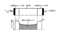
- the PiN diode has a high-concentration p-type layer (hole injection means) 23 on the anode electrode 21 side and a high-concentration n-type layer (electron injection means) 24 on the cathode electrode 22 side.
- the low-concentration n-type layer (i layer) 25 is sandwiched.
- the PiN diode When reverse biasing, most of the reverse voltage is applied to the i layer 25, which is a low-concentration n-type layer having a high resistance value, so the PiN diode has a large reverse voltage withstand capability.
- carriers are injected into the i layer 25 from the high concentration p-type layer 23 and the high concentration n type layer 24 and accumulated in the i layer 25.
- the conductivity in the i layer 25 is modulated (carriers sufficient for conduction are accumulated), and the PiN diode is brought into a conduction state.
- the schematic diagram of FIG. 22 shows the state of carrier distribution during conduction. As can be seen from FIG. 22, during conduction, a large number of carriers are accumulated in the i layer 25, and the i layer 25 has a low resistance, so that the voltage drop in the i layer 25 portion can be kept low.
- a PN junction exists between the i layer 25 which is a low concentration n-type layer and the high concentration p-type layer 23.
- the voltage drop corresponding to the resistance of the PN junction accounts for most of the forward voltage drop of the PiN diode, and this voltage drop continues to exist as a threshold voltage during forward bias (see FIG. 23). Therefore, the conventional PiN diode has a problem that power corresponding to the forward voltage drop occurs as a loss during the conduction period. This also leads to a problem that the energy efficiency of the rectifier circuit including the PiN diode deteriorates.
- Non-patent document 1 shows a theoretical model of a method for solving the problems of the conventional rectifying semiconductor element as described above.
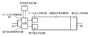
- the essence of this method is to incorporate the operation as a unipolar element into a conventional bipolar element. That is, as shown in FIG. 24, in the bipolar element structure in which the high resistance semiconductor layer 35 is sandwiched between the hole injection means 33 on the anode electrode 31 side and the electron injection means 34 on the cathode electrode 32 side, A signal for switching the hole injection control means 37 and the electron discharge control means 38 alternately is provided by providing the electron discharge means 36 in parallel, the hole injection means 33 and the electron discharge means 36 with the hole injection control means 37 and the electron discharge control means 38, respectively.
- the generating means 39 is provided. Specifically, as shown in FIG.
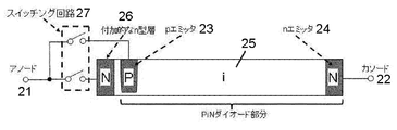
- the n-type layer 26 is added outside the p-type layer 23 on the anode electrode 21 side of the normal PiN diode structure. Then, the anode electrode 21 side is switched to either the p-type layer 23 or the n-type layer 26 by the switching circuit 27 connected to the outside during the forward bias.
- This semiconductor element operates as a bipolar element similar to a conventional PiN diode when the p-type layer 23 is selected, and does not have a PN junction on the current path when the n-type layer 26 is selected. , Operates as a unipolar element.
- the semiconductor device used in this publicly known example is a theoretical model, so that there is a problem that the practicality is poor, such as it is necessary to provide electrodes from three directions, and it is necessary to use an ideal switch as a switch of a switching circuit. is there.
- the prior art has the following problems.
- a voltage drop corresponding to the PN junction existing between the i layer and the high concentration p-type layer continues to exist during forward bias.
- the unipolar semiconductor element has no PN junction in the current path, but has a voltage drop corresponding to the PN junction. Further, the i layer has a higher resistance than the bipolar element even when conducting.
- Non-Patent Document 1 can realize both the electric conduction in the low-resistance i layer of the bipolar element and the electric conduction not through the PN junction of the unipolar element, it is practical for the structure and the external switching element. There are the above difficulties.
- the present invention has been made in consideration of the above circumstances, and can be manufactured by an existing semiconductor element fabrication technique, and even if a switching circuit is not provided outside the element, a loss corresponding to the average value of the forward voltage drop. It is an object of the present invention to provide a diode-structured semiconductor device and a driving method thereof that can reduce energy consumption and increase the energy efficiency of the entire power supply circuit. Also, to provide a rectifying module capable of reducing the loss corresponding to the average value of the forward voltage drop by covering the existing semiconductor device with a switching circuit and increasing the energy efficiency of the entire power supply circuit, and a driving method thereof. With the goal.
- a first configuration of the present invention is a semiconductor device PiN diode having a diode structure in which a p-type layer, an i-layer, and an n-type layer are sequentially formed between an anode electrode and a cathode electrode. And forming a second n-type layer in the p-type layer on the anode electrode side, and switching the anode electrode side to either the p-type layer or the second n-type layer during forward bias Is provided.
- the present invention is a combination of electrical conduction in the i-layer, which is a low resistance of a bipolar rectifier, and electrical conduction not through a PN junction of a unipolar rectifier.
- an electron discharging means is additionally provided on the anode side of a normal rectifying PiN diode.
- the gist of the present invention resides in a semiconductor device capable of realizing the above-described structure and a control means for selectively switching them. Any means may be used as long as the anode side on the current path can be selectively switched between p-type and n-type during forward bias.
- n-type base layer and an n-type emitter layer on the cathode side and a trench structure with a built-in electrode on the anode side and in the case of a normal PiN diode, only a p-type emitter layer exists.
- An n-type layer is also formed, and the anode side is switched to either a p-type layer or an n-type layer using a trench gate.
- the second configuration of the present invention has both the second p-type layer and the second n-type layer on the gate electrode side of the first configuration, and applies a forward bias between the cathode electrode and the anode electrode.
- the semiconductor device includes a gate driving circuit for applying a gate voltage to the gate electrode.
- the gate electrode of the second configuration has a trench structure in contact with the p-type layer, the second p-type layer, and the second n-type layer, and includes an insulating film and an electrode inside the trench.
- This is a semiconductor device.
- the fourth configuration of the present invention is characterized in that the gate electrode of the third configuration forms p-type and n-type channels on the trench surface in accordance with the gate voltage applied from the gate drive circuit. It is a semiconductor device.
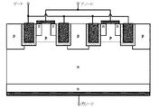
- a semiconductor device having any one of the second to fourth configurations is a basic structural unit, and at least two of the basic structural units are arranged with the anode electrode and the cathode electrode as axes. It is a semiconductor device having a structure that is inverted and combined in line symmetry.
- the sixth configuration of the present invention is a semiconductor device in which three or more basic structural units of the fifth configuration are combined.
- the seventh configuration of the present invention is a semiconductor device in which the anode electrode and the cathode electrode and the n-type layer and the p-type layer in the configurations of the first configuration to the fourth basic structural unit are interchanged.
- the eighth configuration of the present invention includes an n-type layer on the drain side regarded as the cathode electrode in the first to seventh configurations, and both the p-type layer and the n-type layer on the gate / source side regarded as the anode electrode.
- the ninth configuration of the present invention is a semiconductor device in which the transistor element in the eighth configuration is a BSIT (Bipolar Mode Static Induction Transistor) and the switching circuit is a MOSFET (Metal Oxide Semiconductor Field Effect Transistor).
- BSIT Bipolar Mode Static Induction Transistor
- MOSFET Metal Oxide Semiconductor Field Effect Transistor
- the p-type gate region of BSIT is an anode-side hole injection means
- the n-type source region is an anode-side electron discharge means
- the n-type drain region is a cathode-side electron injection means.
- a voltage driving element such as a MOSFET for a switch used in a switching circuit connected to the outside.
- a semiconductor device PiN diode having a diode structure in which a p-type layer, an i-layer, and an n-type layer are sequentially formed between an anode electrode and a cathode electrode
- a method is characterized in that a first operation mode in which a negative voltage is applied to the gate electrode and a second operation mode in which a positive voltage is applied to the gate electrode are alternately repeated at a predetermined period. As described above, by alternately repeating the first operation mode and the second operation mode, it is possible to reduce the loss corresponding to the average value of the forward voltage drop and increase the energy efficiency of the entire power supply circuit.
- the gate charge / discharge time determined by the product of the gate drive resistance value and the gate capacitance is set to the first operation mode and the second operation. It is characterized by being set shorter than the repetition period of the mode.
- a p-type layer is formed on the anode electrode side.
- the second n-type layer is formed therein, and the gate electrode for switching the anode electrode side to either the p-type layer or the second n-type layer is provided during the forward bias.
- the period for selecting a certain hole injecting means and accumulating carriers in the i layer and conducting is alternated with the period for selecting the electron discharging means being the second n-type layer and discharging the carriers from the i layer and conducting them without going through the PN junction.
- (A) And (b) is sectional drawing and a circuit symbol showing the structure of the semiconductor device which concerns on embodiment of this invention. It is sectional drawing showing how to combine the semiconductor device which concerns on embodiment of this invention. It is sectional drawing showing the structural example of the semiconductor device which concerns on embodiment of this invention.
- (A) And (b) is explanatory drawing (PiN mode) showing the operation
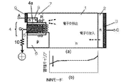
- (A) And (b) is explanatory drawing (NiN mode) showing the operation
- (A) And (b) is a figure showing the dimension and density
- FIG. 14 is a bridge circuit in which the semiconductor device of FIG. 1 and the semiconductor device of FIG. 13 are combined.
- A) And (b) is the schematic diagram and circuit symbol showing the cross section of BSIT.
- A) And (b) is the experimental circuit diagram for demonstration of this invention using BSIT, and a timing chart.
- (A) And (b) is the simple equivalent circuit diagram showing the state at the time of PiN mode operation
- (A) And (b) is the simple equivalent circuit diagram showing the state at the time of NiN mode operation
- (A) And (b) is sectional drawing and a circuit symbol of the structure of the conventional semiconductor element for rectification
- FIG. 6 is a forward characteristic diagram of a conventional rectifying silicon PiN diode. It is a schematic diagram showing the structure of the conventional means for solving the problem of the conventional rectifying semiconductor element. It is sectional drawing of embodiment of the well-known example currently given in the nonpatent literature 1.
- the first conductivity type is n-type and the second conductivity type is p-type.
- the anode electrode side is the first main surface and the cathode electrode side is the second main surface.
- the same reference numerals in the attached drawings denote the same components.
- FIG. 1A is a cross-sectional view showing a basic structural unit of a semiconductor device according to an embodiment of the present invention
- FIG. 1B is a circuit symbol showing the configuration of the semiconductor device.
- an n-type emitter layer 2 of the first conductivity type is formed by diffusion on the second main surface side of the n-type base layer 1 of the first conductivity type.
- a cathode electrode 3 is formed on the surface of the n-type emitter layer 2 on the second main surface side.
- a trench structure 4 is formed on the first main surface side of the n-type base layer 1 so as to bisect the left portion of the element region.
- the trench structure 4 has an insulating film 4 a inside, and the insulating film 4 a is connected to an external gate drive circuit 10 through a gate electrode 5.
- Reference numeral 6 on the first main surface side of the bisected n-type base layer 1 indicates a diffused second conductivity type region, which facilitates hole injection.
- a p-type emitter layer 7 of the second conductivity type is diffused and formed on the opposite side of the p-type region 6 on the first main surface side across the trench structure 4.
- an n-type emitter layer 8 which is an additional first conductivity type for discharging electrons is diffused and formed along the trench structure 4.
- an anode electrode 9 as a high-voltage side main electrode is formed on the surface of the first main surface of both the p-type emitter layer 7 and the n-type emitter layer 8. Is formed.
- the anode electrode 9 is not in contact with the insulating film 4 a of the trench structure 4.
- the semiconductor device configured in this way is driven by different methods at the time of forward bias and reverse bias.
- the first operation mode is a mode in which a negative voltage is applied to one end of the gate resistor Rg by the gate driving circuit 10 and the first main surface side on the current path is selected as the p-type region.
- the gate voltage of the gate electrode 5 begins to drop due to the applied voltage.
- the gate voltage decreases, holes are induced on the surface of the insulating film 4a of the trench structure 4, and the p-type channel layer is formed so as to connect the p-type emitter layer 7 and the p-type region 6. Holes are injected into the n-type base layer 1 from the p-type region 6 and the p-type emitter layer 7 through the p-type channel layer.
- electrons are injected from the n-type emitter layer 2 into the n-type base layer 1.
- An operation period similar to the forward operation of the conventional PiN diode is referred to as a PiN mode. (See Figure 4)
- the second operation mode is a mode in which a positive voltage is applied to one end of the gate resistor Rg by the gate driving circuit 10 and the first main surface side on the current path is selected as the n-type region.
- the gate voltage of the gate electrode 5 starts to rise due to the applied voltage.
- the gate voltage increases, electrons are induced on the surface of the insulating film 4 a of the trench structure 4, and the n-type channel layer is formed so as to connect the n-type emitter layer 8 and the n-type base layer 1.
- Electrons are discharged from the n-type base layer 1 through the n-type channel layer.
- electrons are injected from the n-type emitter layer 2 into the n-type base layer 1.
- This operating period in which the main PN junction does not exist on the current path and conducts with a low forward voltage drop is called the NiN mode. (See Figure 5)
- the p-type and n-type channel layers are selectively formed on one trench structure by controlling the gate voltage as described above between the forward biases, and on the first main surface side.
- a semiconductor device capable of switching between a carrier accumulation process using a hole injection unit and a carrier discharge process using an electron discharge unit can be provided.
- the voltage applied to the gate electrode 5 can be determined by a positive voltage in the PiN mode and a negative voltage in the NiN mode.
- the applied voltage to the gate is lower than the threshold value of the p-channel MOSFET formed by the p-type emitter layer 7, the n-type base layer 1, the p-type region 6, and the gate electrode 5, and in the NiN mode, the n-type emitter layer 8.
- Switching between the PiN mode and the NiN mode described above by making the applied voltage to the gate higher than the threshold value of the n-channel MOSFET formed by the p-type emitter layer 7, the n-type base layer 1, and the gate electrode 5.
- the threshold value of the n-channel MOSFET is 5V
- the voltage applied to the gate is 10V.
- the gate drive circuit 10 continues to apply a negative voltage to one end of the gate resistor Rg.
- the gate voltage decreases, holes are induced on the surface of the insulating film 4a of the trench structure 4, and a p-type channel layer is formed.
- This state is the same as that of the existing PiN diode, and the holes in the n-type base layer 1 are discharged to the first main surface side, and the electrons in the n-type base layer 1 are discharged to the second main surface side.
- a reverse voltage is applied to the n-type base layer 1 whose carriers have been discharged and the resistance value has increased.
- the parameters of the semiconductor device three points of the trench width, the mesa width, and the trench depth) that are considered to be greatly related to the performance of the present invention were evaluated.
- the quality of the present invention is how much the average forward voltage drop can be reduced.
- the simulation method is as follows. First, the semiconductor device is held in the PiN mode for 50 ⁇ s. This is to sufficiently accumulate carriers in the i layer. Next, the semiconductor device is kept in the NiN mode, and the simulation is executed until the calculation diverges (carriers are continuously discharged, the resistivity increases and the forward voltage drop increases).
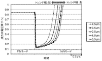
- Fig. 6 shows the simulation results when the trench width is changed. From this result, it can be seen that the longer the trench width, the longer the NiN mode can be maintained.
- Fig. 7 shows the simulation results when the mesa width is changed. From this result, it can be seen that the shorter the mesa width, the longer the NiN mode can be maintained.
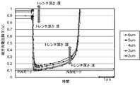
- Fig. 8 shows the simulation results when the trench depth is changed. Although there is no difference in the retention time of the NiN mode with respect to the trench depth, the value of the voltage drop during the PiN mode and the NiN mode is lower when the trench depth is shallower. Therefore, it is better that the trench depth is shallow.
- FIGS. 9A-9A dimensions of each part of the designed semiconductor device, concentrations of each region, and timing charts of gate signals are shown in FIGS.
- the parenthesis indicates the concentration of the region, and the unit is cm ⁇ 3 .
- FIG. 10 shows a simulation result when the two operation modes are repeated by the control signal applied from the gate drive circuit 10 of the embodiment.
- a voltage drop due to carrier accumulation occurs in the PiN mode period in which the p-type channel layer is formed and holes are injected on the first main surface side. This is the same operation as when the existing silicon PiN diode is forward biased.
- the main PN junction does not exist on the current path in the NiN mode period in which the n-type channel layer is formed and electrons are discharged on the first main surface side, the value of the forward voltage drop is low. It is suppressed. For this reason, the present invention can reduce conduction loss as compared with the conventional method in which the built-in potential continues to occur during forward bias.
- the gate charge / discharge time that is, the rise time and the fall time of the pulse waveform in FIG. 10 are determined by the product of the gate drive resistance value (Rgg) and the gate capacitance (Cg) consisting of the gate circuit and in-chip wiring.
- the gate charge / discharge time is required to be shorter than the PiN mode and NiN mode times. That is, if the gate charge / discharge time is long, problems such as delay in hole injection from the channel and insufficient electron discharge occur, and as a result, the conduction loss cannot be reduced.
- the value of gate charge / discharge time Rgg ⁇ Cg was set to 0.1 ⁇ sec.
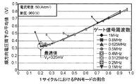
- FIG. 11 is a graph obtained by plotting the result of calculating the average value of the forward voltage drop by executing the simulation of the above embodiment at various gate signal frequencies using the semiconductor device in FIG.
- the vertical axis in the figure represents the average value of the forward voltage drop
- the horizontal axis represents the ratio of the PiN mode when the PiN mode and NiN mode group is one cycle.
- the optimum value is obtained when the PiN mode ratio is around 0.2 (NiN mode ratio is 0.8), and the optimum value increases as the frequency decreases.
- FIG. 12 is a graph in which the conduction loss due to the forward voltage drop that can be reduced and the gate drive loss that occurs to drive the trench gate are added together and compared for each gate signal frequency.
- the vertical axis represents the drive loss of the element per unit area, and the horizontal axis represents the gate signal frequency. From FIG. 12, it can be seen that the conduction loss corresponding to the forward voltage drop increases as the frequency is lower because the reduction effect is smaller, but the gate drive loss is smaller and the sum of the losses is larger. As the frequency increases, the gate drive loss increases, but the conduction loss corresponding to the forward voltage drop decreases at a rate higher than that, so the sum of losses decreases.
- the configuration of only the basic structural unit shown in FIG. 1 is sufficient.
- the flowing current can be dispersed. This leads to more uniform injection of carriers into the i layer.
- the present invention can flexibly cope with the voltage / current class in which the rectifying element is used by changing the number of combinations of basic structural units.
- FIG. 13 shows a semiconductor device in which the anode and cathode, and the n-type layer and p-type layer of the semiconductor device of the basic structural unit shown in FIG. 1 are exchanged.
- This semiconductor device is provided with a trench structure 14 on the cathode side, and is switched between a PiN mode and a PiP mode by a gate signal. Since the PiP mode operates as a unipolar element similarly to the NiN mode, the main PN junction does not exist on the current path, and conducts with a low forward voltage drop.
- 11 is a first conductivity type base layer
- 12 is a first conductivity type emitter layer
- 13 is an anode electrode as a high voltage side main electrode
- 15 is a gate electrode
- 16 is a second conductivity type region for discharging electrons
- Reference numeral 17 denotes a second conductivity type emitter layer
- 18 denotes an additional first conductivity type emitter layer for hole injection
- 19 denotes a cathode electrode as a low voltage side main electrode
- 20 denotes a gate drive circuit.
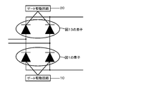
- FIG. 14 is a bridge circuit in which the semiconductor device shown in FIG. 1 and the semiconductor device shown in FIG. 13 are combined. There is an advantage that the number of gate driving circuits can be reduced by combining them.
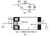
- FIG. 15 shows a schematic diagram and a circuit symbol of the internal structure of the BSIT.
- the BSIT has a p-type gate region and an n-type source region on the anode side when the n-type drain region is regarded as a cathode
- the p-type gate region of BSIT is utilized as anode-side hole injection means
- the n-type source region is utilized as anode-side electron ejection means
- the n-type drain region is utilized as cathode-side electron injection means.
- FIG. 16A shows an experimental circuit diagram for demonstration of this embodiment using BSIT
- FIG. 16B shows a timing chart.
- the operation of the circuit shown in FIG. 16 will be described below.
- the BSIT drain cathode when replaced with a PiN diode
- the MOSFET is turned on and off to replace the BSIT gate and source (PiN diode). Regardless of which region is conducting, the gate and source sides are always kept at a high potential (forward bias when replaced with a PiN diode) during the experiment.
- the conduction period (t 0 to t 1 ) is 500 ⁇ s.
- the switching circuit part is described below.
- the switching circuit portion is composed of a gate signal source and two n-channel and p-channel MOSFETs. Since the MOSFETs are grounded at the source, both MOSFETs can be alternately conducted by a common positive / negative gate signal.
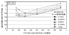
- FIG. 20 is a graph obtained by plotting the result of calculating the average value of the forward voltage drop by performing the experiment of the above-described embodiment using the circuit in FIG. 16 at the gate signal frequencies of various MOSFETs.
- the vertical axis in the figure represents the average value of the forward voltage drop
- the horizontal axis represents the ratio of the PiN mode when the PiN mode and NiN mode group is one cycle.
- the current passed through BSIT was 10A. From FIG. 20, it can be confirmed that the average value of the forward voltage drop can be reduced by about 0.6 V compared to the case where the ratio of the PiN mode is close to 1 (operation close to a normal PiN diode).
- the present invention is suitable for a wide range of uses such as an electrical appliance having a rectifying element or an electronic device as a semiconductor device that reduces the average value of the forward voltage drop and realizes low loss of the rectifying element and its driving method. Can be used.
Landscapes
- Metal-Oxide And Bipolar Metal-Oxide Semiconductor Integrated Circuits (AREA)
- Junction Field-Effect Transistors (AREA)
Abstract
順方向電圧降下の平均値を低減し、整流素子の低損失化を実現する半導体装置とその駆動方法を提供する。 アノード電極9とカソード電極3との間に、p型層7と、i層1と、n型層2とを順に形成したダイオード構造の半導体装置において、アノード電極9側に、p型層7と並列に第2n型層8を形成し、順方向バイアス中に、アノード電極9側をp型層7と第2n型層8のいずれかに切り替えるゲート駆動回路10を備えた半導体装置。ゲート電極5は、p型層7と第2p型層6と第2n型層8に接するトレンチ構造4とし、トレンチ内部に絶縁膜4aと電極とを備えたものとすることができる。このゲート電極5は、ゲート駆動回路10から印加するゲート電圧に応じてp型及びn型のチャネルをトレンチ表面に形成する。
Description
本発明は、低損失なダイオード構造の半導体装置及びその駆動方法に関する。
家庭で使われる多くの電化製品には交直変換用の整流回路が組み込まれており、その中のダイオードブリッジ回路の部分には整流用素子としてバイポーラ素子であるシリコンPiNダイオードが多く使われている。PiNダイオードは、図21に示すように、アノード電極21側の高濃度p型層(ホールの注入手段)23と、カソード電極22側の高濃度n型層(電子の注入手段)24とで、低濃度n型層(i層)25を挟み込む構造をしている。
逆方向バイアス時には逆方向電圧のほとんどは抵抗値の高い低濃度n型層であるi層25に印加されるのでPiNダイオードは大きな逆電圧耐量を持つ。順方向バイアス時には、キャリアが高濃度p型層23及び高濃度n型層24からi層25に注入され、i層25内に蓄積される。これにより、i層25内の伝導度が変調され(導通に十分なキャリアが蓄積され)PiNダイオードは導通状態に至る。導通時のキャリアの分布の様子を、図22の模式図に示す。図22から分かるように、導通時はi層25内に多くのキャリアが蓄積され、i層25は低抵抗となっているためi層25部分での電圧降下は低く抑えられる。
しかし、低濃度n型層であるi層25と高濃度p型層23との間にはPN接合が存在している。このPN接合の抵抗に相当する電圧降下がPiNダイオードの順方向電圧降下の大半を占めており、この電圧降下が、順方向バイアス時に閾値電圧として存在し続ける(図23参照)。そのため、従来のPiNダイオードではこの順方向電圧降下分の電力が、損失として導通期間中生じるという問題がある。このことはPiNダイオードを包含する整流回路のエネルギー効率が悪化するという問題にも繋がる。
一方でショットキーバリアダイオードに代表されるようなユニポーラ素子の場合、電流の経路中にPN接合は存在しないが、PN接合に相当する電圧降下は存在し、さらにi層中は導通時もバイポーラ素子に比べユニポーラ素子は高抵抗となるので、この部分における電圧降下が大きくなるという問題がある。
以上に述べたような従来の整流用半導体素子の問題点を解決する方法の理論モデルが非特許文献1に示されている。この方法の骨子は従来のバイポーラ素子にユニポーラ素子としての動作を組み込むことにある。すなわち、図24に示すように、アノード電極31側のホール注入手段33と、カソード電極32側の電子注入手段34とで、高抵抗半導体層35を挟み込んだバイポーラ素子構造において、ホール注入手段33と並列に電子排出手段36を設け、ホール注入手段33と電子排出手段36にホール注入制御手段37と電子排出制御手段38をそれぞれ設け、ホール注入制御手段37と電子排出制御手段38を交互に切り替える信号発生手段39を設けたものである。具体的には、図25に示すように、通常のPiNダイオード構造のアノード電極21側であって、p型層23の外側にn型層26を追加した構造である。そして、順方向バイアス中に外部に接続したスイッチング回路27によって、アノード電極21側がp型層23とn型層26のいずれかに切り替えられる。この半導体素子では、p型層23が選択されているときは従来のPiNダイオードと同様のバイポーラ素子として動作し、n型層26が選択されているときは電流の経路上にPN接合が存在しない、ユニポーラ素子として動作する。
この方法を用いることでi層25にキャリアを注入する合間に、PN接合を介さない電気伝導を行うことができ、その期間だけバイポーラ素子と比較し順方向電圧降下を低減できる。結果として順方向電圧降下の平均値が低減でき、導通損失を低減できる。
しかし、この公知例で使用されている半導体装置は理論モデルであり、そのため電極を3方向から出す必要がある、スイッチング回路のスイッチに理想スイッチを使う必要がある、など実用性に乏しいという問題がある。
Yasuaki Matsumoto, Kenichi Takahama, and Ichiro Omura "Challenge to the Barrier of Conduction Loss in PiN Diode toward VF<300mV with Pulsed Carrier Injection Concept", Proc. of ISPSD 2010, pp.119-122, 2010.
上述したように、従来技術には以下に述べるような問題点がある。
バイポーラ半導体素子は、i層と高濃度p型層との間に存在しているPN接合に相当する電圧降下が順方向バイアス時に存在し続ける。
バイポーラ半導体素子は、i層と高濃度p型層との間に存在しているPN接合に相当する電圧降下が順方向バイアス時に存在し続ける。
ユニポーラ半導体素子は、電流の経路中にPN接合は存在しないが、PN接合に相当する電圧降下は存在し、さらにi層中は導通時もバイポーラ素子に比べ高抵抗となる。
前掲の非特許文献1において提案された半導体素子は、バイポーラ素子の低抵抗なi層における電気伝導とユニポーラ素子のPN接合を介さない電気伝導の両立を実現できるものの、構造や外部スイッチング素子に実用上の難点がある。
本発明は上記実情を考慮してなされたもので、既存の半導体素子作製技術で製造することが可能で、素子外部にスイッチング回路を持たなくても、順方向電圧降下の平均値に相当する損失を低減し、電源回路全体のエネルギー効率を上げることのできるダイオード構造の半導体装置とその駆動方法を提供することを目的とする。また、既存の半導体装置にスイッチング回路を外装することで順方向電圧降下の平均値に相当する損失を低減し、電源回路全体のエネルギー効率を上げることのできる整流モジュールとその駆動方法を提供することを目的とする。
前記課題を解決するため、本発明の第1の構成は、アノード電極とカソード電極との間に、p型層と、i層と、n型層とを順に形成したダイオード構造の半導体装置PiNダイオードにおいて、前記アノード電極側に、前記p型層内に第2n型層を形成し、順方向バイアス中に、前記アノード電極側を前記p型層と前記第2n型層のいずれかに切り替えるゲート電極を設けたことを特徴とする。
本発明は、バイポーラ整流素子の低抵抗であるi層における電気伝導と、ユニポーラ整流素子のPN接合を介さない電気伝導を組み合わせたものである。通常の整流用PiNダイオードのアノード側に、ホール注入手段だけでなく、電子排出手段を付加的に持つ構造としたものである。本発明の骨子は上述の構造を実現できる半導体装置と、それらを選択的に切り替える制御手段にある。順方向バイアス時に電流経路上のアノード側をp型とn型とで選択的に切り替えられるものであればどのような手段でもよい。
例えば、高抵抗のn型ベース層とカソード側にn型エミッタ層を備え、アノード側に電極を内蔵したトレンチ構造を有し、通常のPiNダイオードの場合にはp型エミッタ層のみ存在するところにn型層も形成し、トレンチゲートを利用してアノード側をp型層と、n型層のいずれかに切り替える。これにより、素子外部にスイッチング回路を持たなくても、順方向電圧降下の平均値に相当する損失を低減し、電源回路全体のエネルギー効率を上げることができる。
本発明の第2の構成は、第1の構成のゲート電極側に第2p型層と前記第2n型層の両方を有し、前記カソード電極と前記アノード電極との間に順方向バイアスを印加中に、前記ゲート電極にゲート電圧を印加するゲート駆動回路を備えた半導体装置である。
本発明の第3の構成は、第2の構成のゲート電極は、前記p型層と前記第2p型層と前記第2n型層に接するトレンチ構造とし、トレンチ内部に絶縁膜と電極とを備えたことを特徴とする半導体装置である。
本発明の第4の構成は、第3の構成のゲート電極は、ゲート駆動回路から印加するゲート電圧に応じてp型及びn型のチャネルをトレンチ表面に形成するものであることを特徴とする半導体装置である。
本発明の第5の構成は、第2から第4のいずれかの構成の半導体装置を基本構成単位とし、この基本構成単位の少なくとも2個を、前記アノード電極と前記カソード電極間を軸にして線対称に反転させて組み合わせた構造を有する半導体装置である。
本発明の第6の構成は、第5の構成の基本構成単位を、3個以上組み合わせた半導体装置である。
本発明の実施にあたっては第1の構成~第4の構成の基本構成単位のみの構成で十分であるが、第5の構成あるいは第6の構成のように、基本構成単位を複数個組み合わせることで、一つ一つのチャネルに流れる電流が分散できる。このことはより均等にi層内にキャリアを注入することに繋がる。
本発明の第7の構成は、第1の構成~第4の基本構成単位の構成のアノード電極とカソード電極、n型層とp型層を入れ替えた半導体装置である。
本発明の第8の構成は、第1の構成~第7の構成においてカソード電極とみなすドレイン側にn型層を備え、アノード電極とみなすゲート・ソース側にp型層とn型層の両方を備えるトランジスタ素子のゲート・ソース側にスイッチング回路を組み合わせた半導体装置である。
本発明の第9の構成は、第8の構成におけるトランジスタ素子は、BSIT(Bipolar Mode Static Induction Transistor)であり、スイッチング回路はMOSFET(Metal Oxide Semiconductor Field Effect Transistor)を使用する半導体装置である。
前記の第8及び第9の構成においては、BSITのp型ゲート領域をアノード側のホール注入手段、n型ソース領域をアノード側の電子排出手段、n型ドレイン領域をカソード側の電子注入手段として利用する。外部に接続するスイッチング回路に用いるスイッチにはMOSFETのような電圧駆動素子を用いることが望ましい。
本発明の第10の構成は、アノード電極とカソード電極との間に、p型層と、i層と、n型層とを順に形成したダイオード構造の半導体装置PiNダイオードにおいて、前記アノード電極側に、前記p型層内に第2n型層を形成し、順方向バイアス中に、前記アノード電極側を前記p型層と前記第2n型層のいずれかに切り替えるゲート電極を設けた半導体装置の駆動方法であって、前記ゲート電極に負の電圧を印加する第1の動作モードと、前記ゲート電極に正の電圧を印加する第2の動作モードを所定周期で交互に繰り返すことを特徴とする。このように、第1の動作モードと第2の動作モードを交互に繰り返すことにより、順方向電圧降下の平均値に相当する損失を低減し、電源回路全体のエネルギー効率を上げることができる。
本発明の第11の構成は、第10の構成の半導体装置の駆動方法において、ゲート駆動の抵抗値とゲート容量の積より決まるゲート充放電時間を、前記第1の動作モードと第2の動作モードの繰り返し周期よりも短く設定することを特徴とする。このようにゲート充放電時間を設定することにより、チャネルからのホールの注入が速くなり、電子の排出を十分に行うことができ、導通損失の低減を図ることができる。
本発明によれば、アノード電極とカソード電極との間に、p型層と、i層と、n型層とを順に形成したダイオード構造の半導体装置PiNダイオードにおいて、アノード電極側に、p型層内に第2n型層を形成し、順方向バイアス中に、アノード電極側をp型層と第2n型層のいずれかに切り替えるゲート電極を設けたことにより、順方向バイアス時に、p型層であるホール注入手段を選択しキャリアをi層内に蓄積し導通させる期間と、第2n型層である電子排出手段を選択しキャリアをi層から排出し、PN接合を介さず導通させる期間を交互に繰り返すことによって順方向電圧降下の平均値を低減し、整流素子の低損失化を実現する。
以下、本発明の実施の形態について図面を参照しつつ詳細に説明する。なお、以下の実施形態では第1導電型をn型、第2導電型をp型としている。そして、アノード電極側を第一の主面、カソード電極側を第二の主面としている。添付図面中の同じ参照符号は同等の構成を示すものである。
図1(a)は、本発明の実施形態に係る半導体装置の基本構成単位を示す断面図、図1(b)は、この半導体装置の構成を示す回路記号である。図1において、第1導電型であるn型ベース層1の第二の主面側には、第1導電型であるn型エミッタ層2が拡散形成されている。n型エミッタ層2の第二の主面側の表面には低電圧側主電極としてのカソード電極3が形成されている。
一方、n型ベース層1の第一の主面側には素子領域の左部を二分する形でトレンチ構造4が形成されている。トレンチ構造4は、その内部に絶縁膜4aを有しており、該絶縁膜4aはゲート電極5を介して、外部のゲート駆動回路10に接続される。二分されたn型ベース層1の第一の主面側の参照符号6は拡散形成された第2導電型領域を示しており、ホールの注入を行いやすくする。
また、第一の主面側のp型領域6とはトレンチ構造4を挟んで反対側に、第2導電型であるp型エミッタ層7が拡散形成されている。p型エミッタ層7の内部には電子排出用の付加的な第1導電型であるn型エミッタ層8が上記トレンチ構造4に沿うように拡散形成されている。前記n型エミッタ層8のトレンチ構造4と反対側には、p型エミッタ層7とn型エミッタ層8の両方の第一の主面側の表面に高電圧側主電極としてのアノード電極9が形成されている。ただし、アノード電極9はトレンチ構造4の絶縁膜4aとは接していない構造とする。
このように構成された半導体装置は順方向バイアス時と逆方向バイアス時に、それぞれ異なる方式で駆動される。
始めにカソード電極3に対してアノード電極9に正の電圧が印加されている順方向バイアス時の動作について述べる。この状況下では、図1に示した半導体装置はゲート駆動回路10から印加される制御信号によって2つの動作モードを繰り返す形で駆動される。
1つ目の動作モードは、ゲート駆動回路10によってゲート抵抗Rgの一端に負の電圧を印加し、電流経路上での第一の主面側をp型領域に選択するモードである。このとき、印加電圧によってゲート電極5のゲート電圧が下がり始める。ゲート電圧の低下に伴い、トレンチ構造4の絶縁膜4a表面にホールが誘起され、p型チャネル層がp型エミッタ層7とp型領域6を繋ぐような形で形成される。このp型チャネル層を介して、p型領域6及びp型エミッタ層7からn型ベース層1内にホールが注入される。この間、n型エミッタ層2からは、電子がn型ベース層1に注入されている。この従来のPiNダイオードの順方向動作と同様の動作期間を、PiNモードと呼ぶ。(図4参照)
2つ目の動作モードは、ゲート駆動回路10によってゲート抵抗Rgの一端に正の電圧を印加し、電流経路上での第一の主面側をn型領域に選択するモードである。このとき、印加電圧によってゲート電極5のゲート電圧が上がり始める。ゲート電圧の増加に伴い、トレンチ構造4の絶縁膜4a表面に電子が誘起され、n型チャネル層がn型エミッタ層8とn型ベース層1を繋ぐような形で形成される。このn型チャネル層を介して、n型ベース層1から電子が排出される。この間も、n型エミッタ層2からは、電子がn型ベース層1に注入されている。主たるPN接合が電流経路上に存在せず、低い順方向電圧降下で導通するこの動作期間を、NiNモードと呼ぶ。(図5参照)
この実施の形態では順方向バイアス間において、上述のようにゲート電圧を制御することで1つのトレンチ構造上にp型とn型のチャネル層を選択的に形成し、第一の主面側でホール注入手段を用いたキャリアの蓄積過程と電子排出手段を用いたキャリアの排出過程とを切り替えることが可能な半導体装置を提供できる。
ゲート電極5に印加する電圧は、PiNモードでは正の電圧、NiNモードでは負の電圧によりモードを決定することができる。PiNモードでは、p型エミッタ層7、n型ベース層1、p型領域6、及びゲート電極5で形成されたpチャネルMOSFETの閾値よりゲートへの印加電圧を低く、NiNモードではn型エミッタ層8、p型エミッタ層7、n型ベース層1、及びゲート電極5で形成されたnチャネルMOSFETの閾値よりゲートへの印加電圧を高くすることで、上記で説明したPiNモードとNiNモードの切り替えが可能となる。たとえば、今回解析した素子では、nチャネルMOSFETの閾値が5Vであり、ゲートへの印加電圧は10Vとしている。
次にカソード電極3に対してアノード電極9に負の電圧が印加されている逆方向バイアス時の動作について述べる。この状況下では、ゲート駆動回路10によってゲート抵抗Rgの一端に負の電圧が印加され続ける。ゲート電圧の低下に伴い、トレンチ構造4の絶縁膜4aの表面にホールが誘起され、p型チャネル層が形成される。この状態は既存のPiNダイオードと同じであり、n型ベース層1内のホールは第一の主面側へ排出され、n型ベース層1内の電子は第二の主面側へ排出される。キャリアが排出され抵抗値の高くなったn型ベース層1に逆方向電圧が印加される。
本実施の形態においてシミュレーションを実行するにあたり、本発明の性能に大きく関わりがあると考えられる半導体装置のパラメータ(トレンチ幅、メサ幅、トレンチ深さの3点)について評価を行った。本発明の特性の良し悪しはどれだけ順方向電圧降下の平均値を低減できるかということである。特性を良くするためには、NiNモードの期間を可能な限り長くすることが必要となる。そこで評価を行う上での判断基準としては、NiNモードを維持できる時間の長短とする。
シミュレーション方法は以下の通りである。初めに半導体装置をPiNモードで50μs間保持する。これはi層中に十分キャリアを蓄積させるためである。次に半導体装置をNiNモードに保持し続けて、計算が発散する(キャリアが排出され続けて、抵抗率が上昇し順方向電圧降下が大きくなる)までシミュレーションを実行する。
図6にトレンチ幅を変えた場合のシミュレーション結果を示す。この結果より、トレンチ幅は長い方がより長くNiNモードを保持できることが分かる。
図7にメサ幅を変えた場合のシミュレーション結果を示す。この結果より、メサ幅は短い方がより長くNiNモードを保持できることが分かる。
図8にトレンチ深さを変えた場合のシミュレーション結果を示す。トレンチ深さについてはNiNモードの保持時間に差はないが、PiNモード及びNiNモード期間中の電圧降下の値はトレンチ深さが浅い方が低い。したがってトレンチ深さは浅い方が良い。
以上のシミュレーション結果を踏まえ、設計した半導体装置の各部の寸法と各領域の濃度及びゲート信号のタイミングチャートを図9(a)、(b)に示す。図9(a)の半導体装置の断面図において括弧表示で示しているのは、その領域の濃度であり、単位はcm-3である。
図10に実施例のゲート駆動回路10から印加される制御信号によって2つの動作モードを繰り返しているときのシミュレーション結果を示す。図10より分かるように、p型チャネル層が形成され、第一の主面側でホールが注入されているPiNモード期間ではキャリア蓄積に伴う電圧降下が生じている。これは既存のシリコンPiNダイオードの順方向バイアス時と同様の動作である。一方で、n型チャネル層が形成され、第一の主面側で電子が排出されているNiNモード期間では電流の経路上に主なPN接合が存在しないため、順方向電圧降下の値は低く抑えられている。このため、本発明は、順方向バイアス時にビルトインポテンシャルが生じ続ける従来の方法と比較し、導通損失を低減できる。
ゲート回路及びチップ内配線からなるゲート駆動の抵抗値(Rgg)とゲート容量(Cg)の積により、ゲート充放電時間、すなわち図10のパルス状波形の立ち上がり時間、立ち下がり時間が決まる。ゲートの充放電時間はPiNモード、NiNモードの時間に比べ短いことが要求される。すなわち、ゲート充放電時間が長いと、チャネルからのホールの注入が遅れる、電子の排出が十分にできないなどの問題が起こり、結果として導通損失の低減ができなくなる。今回の解析ではゲート充放電時間=Rgg×Cgの値が0.1μ秒になるようにした。
図11は、図1における半導体装置を用いて、様々なゲート信号周波数で上述の実施形態のシミュレーションを実行し、順方向電圧降下の平均値を計算した結果をプロットしたグラフである。図の縦軸は順方向電圧降下の平均値を表し、横軸はPiNモードとNiNモードの組を1サイクルとしたときのPiNモードの割合を示している。図11から、周波数が高い場合にはPiNモードの割合が0.2付近(NiNモードの割合が0.8)で最適値が得られ、周波数が低くなるにつれて最適値が高くなることが分かる。
順方向電圧降下の平均値を低減するという観点からは、1サイクルの中で可能な限りNiNモード(キャリアの排出過程)の割合を増やすことが望ましいが、PiNモード(キャリアの注入過程)が短すぎるとn型ベース層1の抵抗率が大きくなり、結果として順方向電圧降下の平均値を上昇させることにつながる。この実施例のように周波数に応じてPiNモードとNiNモードの割合には最適な比率があり、この比率から逸脱しないように制御を行うことが肝要である。
図12は、低減できた順方向電圧降下による導通損失とトレンチゲートを駆動させるために生じるゲートドライブ損失とを足し合わせ、ゲート信号周波数ごとに比較したグラフである。縦軸は、単位面積当たりの素子の駆動損失を表し、横軸はゲート信号周波数を表す。図12から、順方向電圧降下分に相当する導通損失は、周波数が低いほうが低減効果は小さいため大きくなるが、ゲートドライブ損失は小さく、損失の和としては大きくなることが分かる。周波数が高くなるにつれてゲートドライブ損失は大きくなるが順方向電圧降下分に相当する導通損失がそれを上回る割合で小さくなるため、損失の和は減少する。しかし、周波数がさらに高くなると順方向電圧降下分に相当する導通損失は横ばいになる一方、ゲートドライブ損失の増加が顕著となり、損失の和は再び大きくなる。したがって、本実施例の駆動に係るゲート駆動周波数としては本発明の駆動損失が従来素子に比べ、約半分にまで低減できる数百kHzが妥当であると言える。
なお、本発明の実施にあたっては図1に示した基本構成単位のみの構成で十分であるが、図2、図3に示すように基本構成単位を複数個組み合わせることで、一つ一つのチャネルに流れる電流が分散できる。このことはより均等にi層内にキャリアを注入することに繋がる。また、本発明は整流素子が利用される電圧・電流階級に、基本構成単位の組み合わせ数を変えることで柔軟に対応することができる。
図13は、図1に示した基本構成単位の半導体装置のアノードとカソード、n型層とp型層を入れ替えた半導体装置である。この半導体装置はカソード側にトレンチ構造14を設けており、ゲート信号によりPiNモードとPiPモードに切り替える。PiPモードはNiNモードと同様にユニポーラ素子として動作するため、主たるPN接合が電流経路上に存在せず、低い順方向電圧降下で導通する。図中、11は第1導電型ベース層、12は第1導電型エミッタ層、13は高電圧側主電極としてのアノード電極、15はゲート電極、16は電子排出用の第2導電型領域、17は第2導電型エミッタ層、18はホール注入用の付加的な第1導電型エミッタ層、19は低電圧側主電極としてのカソード電極、20はゲート駆動回路である。
図14は、図1に示した半導体装置と図13に示した半導体装置を組み合わせたブリッジ回路である。組み合わせることによりゲート駆動回路を少なくできる利点がある。
次に本発明の第8または第9の構成に対応する実施の形態について以下に述べる。BSITの内部構造の模式図と回路記号を図15に示す。図15から分かるようにBSITはn型のドレイン領域をカソードと見なせばアノード側にp型のゲート領域とn型のソース領域を持つので、図24に示した本発明の前提となる実施条件を備えていると見なせる。BSITのp型ゲート領域をアノード側のホール注入手段、n型ソース領域をアノード側の電子排出手段、n型ドレイン領域をカソード側の電子注入手段として利用する。
図16(a)にBSITを用いた本実施の形態の実証用実験回路図を、図16(b)にタイミングチャートを示す。図16に示す回路の動作について以下に述べる。時刻t=t0でswがONするとBSITのドレイン(PiNダイオードに置き換えるとカソード)側がグランドに対して負の電位になるので、MOSFETをON/OFFさせてBSITのゲート、ソース(PiNダイオードに置き換えるとアノード)どちらの領域が導通しても実験中は常にゲート、ソース側が高電位(PiNダイオードに置き換えると順方向バイアス)に維持される。導通期間(t0~t1)は500μsとする。
スイッチング回路部分について以下に述べる。スイッチング回路部分はゲート信号源とnチャネルとpチャネルの2つのMOSFETで構成される。MOSFETはソース接地しているので共通の正負ゲート信号で両方のMOSFETを交互に導通させることができる。
MOSFETのゲートに+10Vが印加されているときは回路図中の上側のnチャネルMOSがONする。この時、BSITのp型ゲート領域からホールが注入され、n型ドレイン領域から電子が注入される。これはPiNモードとみなせる。(図17参照)
MOSFETのゲートに-10Vが印加されているときは回路図中の下側のpチャネルMOSがONする。この時、BSITのn型ソース領域から電子が排出され、n型ドレイン領域から電子が注入される。これはNiNモードとみなせる。(図18参照)
実験結果を図19に示す。図19より分かるように、p型ゲート領域が選択され、ホールが注入されている期間ではキャリア蓄積に伴う電圧降下が生じている。これは既存のシリコンPiNダイオードの順方向バイアス時と同様の動作である(PiNモード)。一方で、n型ソース領域が選択され、電子が排出されている期間では電流の経路上に主なPN接合が存在しないため、順方向電圧降下の値は低く抑えられている(NiNモード)。このため、この実施例においても順方向バイアス時にビルトインポテンシャルが生じ続ける従来の方法と比較し、導通損失を低減できる。
図20は図16における回路を用いて、様々なMOSFETのゲート信号周波数で上述の実施形態の実験を実行し、順方向電圧降下の平均値を計算した結果をプロットしたグラフである。図の縦軸は順方向電圧降下の平均値を表し、横軸はPiNモードとNiNモードの組を1サイクルとしたときのPiNモードの割合を示している。BSITに流す電流は10Aとした。図20より、PiNモードの割合が1に近い場合(通常のPiNダイオードに近い動作)に比べ0.6V近く順方向電圧降下の平均値を低減できることが確認できる。
本発明は、順方向電圧降下の平均値を低減し、整流素子の低損失化を実現する半導体装置とその駆動方法として、整流素子を有する電化製品、あるいは電子機器等の広範囲な用途に好適に利用することができる。
1 第1導電型ベース層
2 第1導電型エミッタ層
3 低電圧側主電極としてのカソード電極
4 トレンチ構造
4a 絶縁膜
5 ゲート電極
6 ホール注入用の第2導電型領域
7 第2導電型エミッタ層
8 電子排出用の付加的な第1導電型エミッタ層
9 高電圧側主電極としてのアノード電極
10 ゲート駆動回路
Rg ゲート抵抗
11 第1導電型ベース層
12 第1導電型エミッタ層
13 高電圧側主電極としてのアノード電極
14 トレンチ構造
15 ゲート電極
16 電子排出用の第2導電型領域
17 第2導電型エミッタ層
18 ホール注入用の付加的な第1導電型エミッタ層
19 低電圧側主電極としてのカソード電極
20 ゲート駆動回路
2 第1導電型エミッタ層
3 低電圧側主電極としてのカソード電極
4 トレンチ構造
4a 絶縁膜
5 ゲート電極
6 ホール注入用の第2導電型領域
7 第2導電型エミッタ層
8 電子排出用の付加的な第1導電型エミッタ層
9 高電圧側主電極としてのアノード電極
10 ゲート駆動回路
Rg ゲート抵抗
11 第1導電型ベース層
12 第1導電型エミッタ層
13 高電圧側主電極としてのアノード電極
14 トレンチ構造
15 ゲート電極
16 電子排出用の第2導電型領域
17 第2導電型エミッタ層
18 ホール注入用の付加的な第1導電型エミッタ層
19 低電圧側主電極としてのカソード電極
20 ゲート駆動回路
Claims (11)
- アノード電極とカソード電極との間に、p型層と、i層と、n型層とを順に形成したダイオード構造の半導体装置PiNダイオードにおいて、前記アノード電極側に、前記p型層内に第2n型層を形成し、順方向バイアス中に、前記アノード電極側を前記p型層と前記第2n型層のいずれかに切り替えるゲート電極を設けたことを特徴とする半導体装置。
- 前記ゲート電極側に第2p型層と前記第2n型層の両方を有し、前記カソード電極と前記アノード電極との間に順方向バイアスを印加中に、前記ゲート電極にゲート電圧を印加するゲート駆動回路を備えた請求項1記載の半導体装置。
- 前記ゲート電極は、前記p型層と前記第2p型層と前記第2n型層に接するトレンチ構造とし、トレンチ内部に絶縁膜と電極とを備えたことを特徴とする請求項2記載の半導体装置。
- 前記ゲート電極は、ゲート駆動回路から印加するゲート電圧に応じてp型及びn型のチャネルをトレンチ表面に形成するものである請求項3記載の半導体装置。
- 請求項2から4のいずれかに記載の半導体装置を基本構成単位とし、この基本構成単位の少なくとも2個を、前記アノード電極と前記カソード電極間を軸にして線対称に反転させて組み合わせた構造を有する半導体装置。
- 前記基本構成単位を、3個以上組み合わせた請求項5記載の半導体装置。
- 請求項1から4のいずれかの項に記載の半導体装置のアノード電極とカソード電極、n型層とp型層を入れ替えた半導体装置。
- カソード電極とみなすドレイン側にn型層を備え、アノード電極とみなすゲート・ソース側にp型層とn型層の両方を備えるトランジスタ素子のゲート・ソース側にスイッチング回路を組み合わせた請求項1から7のいずれかの項に記載の半導体装置。
- 前記トランジスタ素子は、BSITであり、スイッチング回路はMOSFETを使用することを特徴とする請求項7記載の半導体装置。
- アノード電極とカソード電極との間に、p型層と、i層と、n型層とを順に形成したダイオード構造の半導体装置PiNダイオードにおいて、前記アノード電極側に、前記p型層内に第2n型層を形成し、順方向バイアス中に、前記アノード電極側を前記p型層と前記第2n型層のいずれかに切り替えるゲート電極を設けた半導体装置の駆動方法であって、前記ゲート電極に負の電圧を印加する第1の動作モードと、前記ゲート電極に正の電圧を印加する第2の動作モードを所定周期で交互に繰り返すことを特徴とする半導体装置の駆動方法。
- ゲート駆動の抵抗値とゲート容量の積より決まるゲート充放電時間を、前記第1の動作モードと第2の動作モードの繰り返し周期よりも短く設定することを特徴とする請求項10記載の半導体装置の駆動方法。
Applications Claiming Priority (2)
| Application Number | Priority Date | Filing Date | Title |
|---|---|---|---|
| JP2011-111883 | 2011-05-18 | ||
| JP2011111883A JP5804494B2 (ja) | 2011-05-18 | 2011-05-18 | 半導体装置及びその駆動方法 |
Publications (1)
| Publication Number | Publication Date |
|---|---|
| WO2012157608A1 true WO2012157608A1 (ja) | 2012-11-22 |
Family
ID=47176925
Family Applications (1)
| Application Number | Title | Priority Date | Filing Date |
|---|---|---|---|
| PCT/JP2012/062300 Ceased WO2012157608A1 (ja) | 2011-05-18 | 2012-05-14 | 半導体装置及びその駆動方法 |
Country Status (3)
| Country | Link |
|---|---|
| JP (1) | JP5804494B2 (ja) |
| TW (1) | TW201312761A (ja) |
| WO (1) | WO2012157608A1 (ja) |
Cited By (1)
| Publication number | Priority date | Publication date | Assignee | Title |
|---|---|---|---|---|
| EP4047663A1 (en) * | 2021-02-18 | 2022-08-24 | Infineon Technologies AG | Voltage-controlled bipolar switching device with tfet switching region |
Citations (4)
| Publication number | Priority date | Publication date | Assignee | Title |
|---|---|---|---|---|
| JPH10163469A (ja) * | 1996-11-29 | 1998-06-19 | Toshiba Corp | ダイオードおよびその駆動方法 |
| JPH10327059A (ja) * | 1997-05-23 | 1998-12-08 | Hitachi Ltd | 静電誘導トランジスタの駆動方法及び駆動回路 |
| JP2000512805A (ja) * | 1996-05-15 | 2000-09-26 | シリコニックス・インコーポレイテッド | シンクロナス整流器或いは電圧クランプ用の3端子パワーmosfetスイッチ |
| JP2008539571A (ja) * | 2005-04-28 | 2008-11-13 | シーメンス アクチエンゲゼルシヤフト | 可制御半導体ダイオード、電子部品および電圧中間形コンバータ |
-
2011
- 2011-05-18 JP JP2011111883A patent/JP5804494B2/ja active Active
-
2012
- 2012-05-14 WO PCT/JP2012/062300 patent/WO2012157608A1/ja not_active Ceased
- 2012-05-17 TW TW101117564A patent/TW201312761A/zh unknown
Patent Citations (4)
| Publication number | Priority date | Publication date | Assignee | Title |
|---|---|---|---|---|
| JP2000512805A (ja) * | 1996-05-15 | 2000-09-26 | シリコニックス・インコーポレイテッド | シンクロナス整流器或いは電圧クランプ用の3端子パワーmosfetスイッチ |
| JPH10163469A (ja) * | 1996-11-29 | 1998-06-19 | Toshiba Corp | ダイオードおよびその駆動方法 |
| JPH10327059A (ja) * | 1997-05-23 | 1998-12-08 | Hitachi Ltd | 静電誘導トランジスタの駆動方法及び駆動回路 |
| JP2008539571A (ja) * | 2005-04-28 | 2008-11-13 | シーメンス アクチエンゲゼルシヤフト | 可制御半導体ダイオード、電子部品および電圧中間形コンバータ |
Cited By (2)
| Publication number | Priority date | Publication date | Assignee | Title |
|---|---|---|---|---|
| EP4047663A1 (en) * | 2021-02-18 | 2022-08-24 | Infineon Technologies AG | Voltage-controlled bipolar switching device with tfet switching region |
| US12266718B2 (en) | 2021-02-18 | 2025-04-01 | Infineon Technologies Ag | Voltage-controlled switching device with channel region |
Also Published As
| Publication number | Publication date |
|---|---|
| TW201312761A (zh) | 2013-03-16 |
| JP5804494B2 (ja) | 2015-11-04 |
| JP2012243918A (ja) | 2012-12-10 |
Similar Documents
| Publication | Publication Date | Title |
|---|---|---|
| US7531993B2 (en) | Half bridge circuit and method of operating a half bridge circuit | |
| CN101946324B (zh) | 反向导通半导体元件的驱动方法和半导体装置以及供电装置 | |
| US20080012043A1 (en) | Semiconductor device and method of operating a semiconductor device | |
| CN102347356A (zh) | 具有开关元件和续流二极管的半导体装置及其控制方法 | |
| US20140001512A1 (en) | Semiconductor Device and Power Conversion Apparatus Using the Same | |
| US8653606B2 (en) | Semiconductor device and power conversion device using same | |
| CN109103240B (zh) | 一种低导通功耗绝缘体上硅横向绝缘栅双极型晶体管 | |
| US7723780B2 (en) | Lateral DMOS device structure and manufacturing method thereof | |
| Li et al. | A novel diode-clamped CSTBT with ultra-low on-state voltage and saturation current | |
| US20150144994A1 (en) | Power semiconductor device | |
| CN108122962B (zh) | 一种绝缘栅双极型晶体管 | |
| CN109888006B (zh) | 一种低功耗绝缘体上硅横向绝缘栅双极型晶体管 | |
| CN102064192B (zh) | 一种soi横向绝缘栅双极型晶体管器件 | |
| JP3491049B2 (ja) | 整流素子およびその駆動方法 | |
| CN106711189A (zh) | 一种超结器件 | |
| JP5804494B2 (ja) | 半導体装置及びその駆動方法 | |
| US20150162429A1 (en) | Semiconductor Device and Power Conversion Device Using the Same | |
| CN103606557A (zh) | 一种集成二极管的集电极短路igbt结构 | |
| CN103928507B (zh) | 一种逆导型双栅绝缘栅双极型晶体管 | |
| JP2012099696A (ja) | 半導体装置 | |
| TWI533451B (zh) | 半導體裝置及使用其之電力轉換裝置 | |
| US20150349102A1 (en) | Ti-igbt and formation method thereof | |
| JP2014146765A (ja) | 半導体装置 | |
| CN103887332A (zh) | 一种新型功率半导体器件 | |
| DE112012006906T5 (de) | Halbleitervorrichtung und elektrischer Leistungswandler mit derselben |
Legal Events
| Date | Code | Title | Description |
|---|---|---|---|
| 121 | Ep: the epo has been informed by wipo that ep was designated in this application |
Ref document number: 12785754 Country of ref document: EP Kind code of ref document: A1 |
|
| DPE1 | Request for preliminary examination filed after expiration of 19th month from priority date (pct application filed from 20040101) | ||
| NENP | Non-entry into the national phase |
Ref country code: DE |
|
| 122 | Ep: pct application non-entry in european phase |
Ref document number: 12785754 Country of ref document: EP Kind code of ref document: A1 |