WO2012153375A1 - クロック生成回路 - Google Patents
クロック生成回路 Download PDFInfo
- Publication number
- WO2012153375A1 WO2012153375A1 PCT/JP2011/060584 JP2011060584W WO2012153375A1 WO 2012153375 A1 WO2012153375 A1 WO 2012153375A1 JP 2011060584 W JP2011060584 W JP 2011060584W WO 2012153375 A1 WO2012153375 A1 WO 2012153375A1
- Authority
- WO
- WIPO (PCT)
- Prior art keywords
- clock signal
- delay
- time
- oscillation
- digital converter
- Prior art date
- Legal status (The legal status is an assumption and is not a legal conclusion. Google has not performed a legal analysis and makes no representation as to the accuracy of the status listed.)
- Ceased
Links
Images











Classifications
-
- H—ELECTRICITY
- H03—ELECTRONIC CIRCUITRY
- H03L—AUTOMATIC CONTROL, STARTING, SYNCHRONISATION OR STABILISATION OF GENERATORS OF ELECTRONIC OSCILLATIONS OR PULSES
- H03L7/00—Automatic control of frequency or phase; Synchronisation
- H03L7/06—Automatic control of frequency or phase; Synchronisation using a reference signal applied to a frequency- or phase-locked loop
- H03L7/08—Details of the phase-locked loop
- H03L7/081—Details of the phase-locked loop provided with an additional controlled phase shifter
- H03L7/0812—Details of the phase-locked loop provided with an additional controlled phase shifter and where no voltage or current controlled oscillator is used
- H03L7/0818—Details of the phase-locked loop provided with an additional controlled phase shifter and where no voltage or current controlled oscillator is used the controlled phase shifter comprising coarse and fine delay or phase-shifting means
-
- H—ELECTRICITY
- H03—ELECTRONIC CIRCUITRY
- H03K—PULSE TECHNIQUE
- H03K5/00—Manipulating of pulses not covered by one of the other main groups of this subclass
- H03K5/22—Circuits having more than one input and one output for comparing pulses or pulse trains with each other according to input signal characteristics, e.g. slope, integral
- H03K5/26—Circuits having more than one input and one output for comparing pulses or pulse trains with each other according to input signal characteristics, e.g. slope, integral the characteristic being duration, interval, position, frequency, or sequence
-
- H—ELECTRICITY
- H03—ELECTRONIC CIRCUITRY
- H03L—AUTOMATIC CONTROL, STARTING, SYNCHRONISATION OR STABILISATION OF GENERATORS OF ELECTRONIC OSCILLATIONS OR PULSES
- H03L7/00—Automatic control of frequency or phase; Synchronisation
- H03L7/06—Automatic control of frequency or phase; Synchronisation using a reference signal applied to a frequency- or phase-locked loop
- H03L7/08—Details of the phase-locked loop
- H03L7/081—Details of the phase-locked loop provided with an additional controlled phase shifter
-
- H—ELECTRICITY
- H03—ELECTRONIC CIRCUITRY
- H03L—AUTOMATIC CONTROL, STARTING, SYNCHRONISATION OR STABILISATION OF GENERATORS OF ELECTRONIC OSCILLATIONS OR PULSES
- H03L7/00—Automatic control of frequency or phase; Synchronisation
- H03L7/06—Automatic control of frequency or phase; Synchronisation using a reference signal applied to a frequency- or phase-locked loop
- H03L7/16—Indirect frequency synthesis, i.e. generating a desired one of a number of predetermined frequencies using a frequency- or phase-locked loop
-
- H—ELECTRICITY
- H03—ELECTRONIC CIRCUITRY
- H03L—AUTOMATIC CONTROL, STARTING, SYNCHRONISATION OR STABILISATION OF GENERATORS OF ELECTRONIC OSCILLATIONS OR PULSES
- H03L7/00—Automatic control of frequency or phase; Synchronisation
- H03L7/06—Automatic control of frequency or phase; Synchronisation using a reference signal applied to a frequency- or phase-locked loop
- H03L7/16—Indirect frequency synthesis, i.e. generating a desired one of a number of predetermined frequencies using a frequency- or phase-locked loop
- H03L7/22—Indirect frequency synthesis, i.e. generating a desired one of a number of predetermined frequencies using a frequency- or phase-locked loop using more than one loop
- H03L7/23—Indirect frequency synthesis, i.e. generating a desired one of a number of predetermined frequencies using a frequency- or phase-locked loop using more than one loop with pulse counters or frequency dividers
- H03L7/235—Nested phase locked loops
Definitions
- the present invention relates to a clock generation circuit.
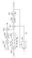
- FIG. 1 is a diagram illustrating a configuration example of a multiphase clock generation circuit.
- the multi-phase clock generation circuit includes a phase-locked loop (PLL) circuit including a phase frequency detector 101, a low-pass filter 102, an oscillator 103, and a frequency divider 104.
- the phase frequency detector 101 compares the phase and frequency between the output clock signal of the frequency divider 104 and the reference clock signal CLK, and outputs the phase difference.
- the low pass filter 102 averages and outputs the phase difference output from the phase frequency detector 101.
- the oscillator 103 generates and outputs a plurality of phase clock signals ⁇ 1 to ⁇ p whose phases are adjusted so that the average value of the differences becomes small.
- the frequency divider 104 divides the clock signal ⁇ 1, for example, and feeds back a clock signal having a frequency lower than that of the clock signal ⁇ 1 to the phase frequency detector 101. By this feedback loop processing, the clock signal ⁇ 1 converges and locks in the same phase as the reference clock signal CLK.
- the multi-phase clock generation circuit of FIG. 1 has the advantage of a simple system and low power consumption.
- the oscillator 103 is a ring oscillator
- the multiphase clock generation circuit of FIG. 1 has a drawback that noise characteristics are lowered and oscillation cannot be performed at a high frequency.
- the multiphase clock generation circuit of FIG. 1 can make the oscillator 103 using a plurality of inductors in order to solve the problem of noise and frequency.
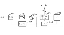
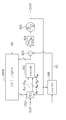
- FIG. 2 is a diagram illustrating a configuration example of another multiphase clock generation circuit.
- the multiphase clock generation circuit of FIG. 2 is obtained by adding a delay line 201, a phase detector 202, and a low-pass filter 203 to the multiphase clock generation circuit of FIG.
- the delay line 201, the phase detector 202, and the low-pass filter 203 constitute a delay-locked loop (DLL) circuit.
- the oscillator 103 outputs a single-phase clock signal to the frequency divider 104, the delay line 201, and the phase detector 202.
- the delay line 201 delays the output clock signal of the oscillator 103 to output a plurality of phase clock signals ⁇ 1 to ⁇ p.
- the phase detector 202 compares the phase of the output clock signal of the oscillator 103 and, for example, the clock signal ⁇ 1, and outputs the phase difference to the low-pass filter 203.
- the low-pass filter 203 averages the phase difference and outputs it to the delay line 201.
- the delay line 201 generates and outputs a plurality of phase clock signals ⁇ 1 to ⁇ p whose phases are adjusted so that the phase difference output from the low-pass filter 203 is small.
- the clock signal ⁇ 1 converges and locks in the same phase as the reference clock signal CLK.
- the multi-phase clock generation circuit of FIG. 2 has an advantage that the noise characteristics of the phase-locked loop circuit can be improved by configuring the oscillator 103 using one inductor.
- the multi-phase clock generation circuit of FIG. 2 requires two low-pass filters 102 and 203, and has a disadvantage that the circuit area is enormous.
- a time digital converter having a coarse time conversion device, a first fine time register, and a second fine time register and combining coarse time conversion and fine time conversion is known (for example, Patent Document 1 and Patent Document). 2).
- An object of the present invention is to provide a high-precision and / or small-sized clock generation circuit capable of generating a multi-phase clock signal.
- the clock generation circuit uses a counter that counts the number of pulses of the oscillation clock signal existing within one cycle of the reference clock signal and a plurality of first delay elements to make the oscillation clock signal relative to the reference clock signal.
- a first time of generating a first clock signal of a plurality of phases by delaying the delay time and outputting a value of the first clock signal of the plurality of phases at the edge time of the reference clock signal as a first digital value By delaying the oscillation clock signal relative to the reference clock signal by using a digital converter and a plurality of second delay elements having a delay time shorter than the delay time of the first delay element, a plurality of phases are obtained.
- Second clock signal is generated, and the value of the second clock signal of the plurality of phases at the edge of the reference clock signal is set to a second digital value.
- the third clock signal of a plurality of phases is generated by delaying the first clock signal relative to the reference clock signal, and the third clock of the plurality of phases at the edge time of the reference clock signal
- a third time digital converter for outputting a signal value as a third digital value; and a period and a target period of the oscillation clock signal obtained based on at least the first digital value and the third digital value;
- An oscillator that generates the oscillation clock signal having a period of 1 / m (m is an integer of 2 or more) of the period of the reference clock signal, and the plurality of first time converters in the first time digital converter
- the delay element changes a delay time according to the delay control signal output from the delay control unit, and the first time digital converter outputs the first clock signal of the plurality of phases.
- the first time digital converter can output a first clock signal having a plurality of phases.
- digital processing becomes possible, so that a highly accurate and / or small clock generation circuit can be provided.
- FIG. 1 is a diagram illustrating a configuration example of a multiphase clock generation circuit.
- FIG. 2 is a diagram illustrating a configuration example of another multiphase clock generation circuit.
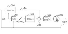
- FIG. 3A is a diagram illustrating a configuration example of a multiphase clock generation circuit using a digital phase lock loop circuit.
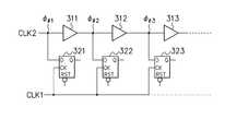
- FIG. 3B is a diagram illustrating a configuration example of the time digital converter of FIG. 3A.
- FIG. 4 is a timing chart showing an example of a multiphase clock signal.
- FIG. 5 is a timing chart for explaining an operation example of the multiphase clock generation circuit.
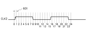
- FIG. 6A is a diagram illustrating the resolution of the oscillation clock signal when the unit delay amount is relatively small.
- FIG. 6B is a diagram illustrating the resolution of the oscillation clock signal when the unit delay amount is relatively large.
- FIG. 7A is a diagram illustrating an example in which a 16-phase clock signal is generated.
- FIG. 7B is a diagram illustrating an example in which an 18-phase clock signal is generated.
- FIG. 8A is a diagram illustrating a configuration example of a multiphase clock generation circuit using a two-stage time digital converter.
- FIG. 8B is a diagram for explaining the operation of the multiphase clock generation circuit of FIG. 8A.
- FIG. 9A is a block diagram illustrating a configuration example of a time digital converter.
- FIG. 9B is a block diagram illustrating a configuration example of the time digital converter.
- FIG. 9C is a time chart for explaining an operation example of the time digital converter.
- FIG. 10A is a diagram illustrating a configuration example of the variable delay element in FIG. 9B.
- FIG. 10B is a diagram illustrating another configuration example of the variable delay element in FIG. 9B.
- FIG. 10C is a diagram illustrating another configuration example of the variable delay element in FIG. 9B.
- FIG. 10D is a diagram illustrating another configuration example of the variable delay element in FIG. 9B.
- FIG. 11A is a diagram for explaining delay time control of the calibration circuit of FIG. 9A.
- FIG. 11B is a diagram for explaining delay time control of the calibration circuit of FIG. 9A.
- FIG. 12 is a time chart showing a state after calibration of the calibration circuit.
- FIG. 13 is a time chart showing a state after calibration of the calibration circuit.
- FIG. 12 is a time chart showing a state after calibration of the calibration circuit.
- FIG. 14A is a diagram illustrating a configuration example of a circuit for normalizing a fine time digital converter to a coarse time digital converter.
- FIG. 14B is a diagram illustrating another configuration example of a circuit for normalizing the fine time digital converter to the coarse time digital converter.
- FIG. 15A is a diagram illustrating a configuration example of a multiphase clock generation circuit according to the second embodiment.
- FIG. 15B is a diagram for explaining the offset lock.
- FIG. 16A is a diagram illustrating an example of convergence of the locked state of the phase-locked loop circuit.
- FIG. 16B is a diagram illustrating an example of convergence of the locked state of the phase-locked loop circuit.
- FIG. 17A is a diagram illustrating a configuration example of a multiphase clock generation circuit according to the third embodiment.
- FIG. 18 is a diagram illustrating a configuration example of the multiphase clock generation circuit according to the first embodiment.
- FIG. 19 is a diagram illustrating a configuration example of a multiphase clock generation circuit according to the fourth embodiment.
- FIG. 20 is a diagram illustrating a configuration example of a multiphase clock generation circuit according to the fifth embodiment.
- FIG. 21 is a diagram illustrating a configuration example of a multiphase clock generation circuit according to the sixth embodiment.
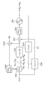
- FIG. 3A is a diagram illustrating a configuration example of a multiphase clock generation circuit using a digital phase lock loop circuit
- FIG. 5 is a timing chart for explaining an operation example of the multiphase clock generation circuit.
- the counter 306 counts the number of pulses EC of the oscillation clock signal CLK2 existing within one cycle of the reference clock signal CLK1.
- the counter 306 counts the number of pulses EC by counting the number of rising edges of the oscillation clock signal CLK2 existing within one period of the reference clock signal CLK1.
- the number of pulses EC is “8”.
- a time digital converter (TDC) 301 receives a reference clock signal CLK1 and an oscillation clock signal CLK2, and generates a plurality of phase clock signals ⁇ 1 to ⁇ p.
- TDC time digital converter
- FIG. 3B is a diagram showing a configuration example of the time digital converter 301 in FIG. 3A
- FIG. 4 is a timing chart showing examples of the multiphase clock signals ⁇ 1 to ⁇ p.
- a series connection circuit such as a plurality of delay elements 311 to 313 sequentially delays the oscillation clock signal CLK2.
- Each of the delay elements 311 to 313 delays the input signal and outputs it.
- the clock signal ⁇ 1 is the same signal as the oscillation clock signal CLK2.
- the clock signal ⁇ 2 is an output signal of the delay element 311.
- the clock signal ⁇ 3 is an output signal of the delay element 312.
- Each phase difference of the clock signals ⁇ 1 to ⁇ 12 corresponds to each delay time of the delay elements 311 to 313 and the like.
- Each of the delay elements 311 to 313 has the same delay time.
- the time digital converter 301 can generate, for example, 12-phase clock signals ⁇ 1 to ⁇ 12.
- the D-type flip-flops 321 to 323 and the like latch the values of the clock signals ⁇ 1 to ⁇ 12 at the time 420 of the rising edge of the reference clock signal CLK1, and output a binary digital value from the Q terminal.
- the D-type flip-flop 321 latches the value of the clock signal ⁇ 1 at the time 420 of the rising edge of the reference clock signal CLK1, and outputs a digital value of “1” from the Q terminal.
- the Q terminals of the D-type flip-flops 321 to 323 and the like output a digital value 421 of “111000000111” as shown in FIG.
- the change point 422 is a point where the digital value 421 changes from “0” to “1”.
- This change point 422 is a phase difference between the oscillation clock signal CLK2 and the reference clock signal CLK1.
- the decoder 302 in FIG. 3A detects the phase difference corresponding to the change point 422.
- the oscillation clock signal CLK2 can be expressed with a resolution of a unit delay amount of 0 to 24, for example.
- a unit delay amount of 0 to 24 corresponds to 24 delay elements 311 to 313 and the like, and a unit delay amount “1” corresponds to a delay time of one delay element.
- the rising edge of the oscillation clock signal CLK2 is detected as a unit delay amount “3” due to a quantization error.
- the corresponding phase difference PE1 corresponds to the phase difference at the change point 422 in FIG. 4 and represents the phase difference of the oscillation clock signal CLK2 with respect to the reference clock signal CLK1.
- the decoder 302 detects the phase difference PE1 of the rising edge of the oscillation clock signal CLK2 with respect to the first rising edge of the reference clock signal CLK1, and similarly oscillates with respect to the second rising edge of the reference clock signal CLK1.
- the phase difference PE2 at the rising edge of the clock signal CLK2 is detected.
- the reference clock signal CLK1 has a cycle Tref from the rising edge at timing t2 to the rising edge at the next timing t2.
- the pulse number EC includes a quantization error and is the maximum pulse number of the oscillation clock signal CLK2 from the timing t1 to the next timing t1.
- the period Tref is expressed by the following equation (1) based on the number of pulses EC and the phase differences PF1 and PF2.
- Tref EC ⁇ PF1 + PF2 (1)
- phase difference PF1 is expressed by the following equation (2) based on the cycle Tv of the oscillation clock signal and the phase difference PE1.
- PF1 Tv ⁇ PE1 (2)
- phase difference PF2 is expressed by the following equation (3) based on the cycle Tv of the oscillation clock signal and the phase difference PE2.
- PF2 Tv ⁇ PE2 (3)
- the period Tv is, for example, the unit delay amount “13” as described above.
- the phase difference PE1 is, for example, a unit delay amount “3”.
- the phase difference PE1 is expressed by a unit delay amount “3/13”.
- the phase difference PE2 is also normalized.
- the decoder 302 and the adder 303 calculate the cycle Tref of the reference clock signal CLK1 by the above equation (1).
- the adder 303 outputs the cycle Tref of the reference clock signal CLK1 to the first low-pass filter 304.
- the first low-pass filter 304 averages and outputs the period Tref of the reference clock signal CLK1 by digital low-pass filtering.
- the oscillator 305 Based on the period Tref of the reference clock signal CLK1 output from the first low-pass filter 304, the oscillator 305 generates an oscillation clock signal CLK2 having a period of 1 / m (m is an integer of 2 or more) of the period Tref of the reference clock signal CLK1. And is fed back to the counter 306 and the time digital converter 301.
- This feedback circuit is a phase-locked loop circuit. The phase difference between the oscillation clock signal CLK2 and the reference clock signal CLK1 approaches 0, and the phase difference converges around 0. That is, for example, the clock signal ⁇ 1 is locked in synchronization with the phase of the reference clock signal CLK1.
- the multiphase clock generation circuit can output a plurality of phase clock signals ⁇ 1 to ⁇ p synchronized with the phase of the reference clock signal CLK1.
- the subsequent stage decoder 302, adder 303 and first low-pass filter 304 can be constituted by digital circuits, so that the multiphase clock generation circuit can be reduced in size and power consumption can be reduced. can do.
- FIG. 6A is a diagram showing the resolution of the oscillation clock signal CLK2 when the unit delay amount is relatively small
- FIG. 6B is a diagram showing the resolution of the oscillation clock signal CLK2 when the unit delay amount is relatively large.
- the magnitude of the unit delay amount “1” is determined by the delay time of the delay element 311 and the like in FIG. 3B.
- the delay time of the delay element 311 and the like dynamically changes depending on process conditions, voltage, and / or temperature. Therefore, there are cases where the unit delay amount “1” is relatively small as shown in FIG. 6A and cases where the unit delay amount “1” is relatively large as shown in FIG. 6B.
- FIG. 6A and 6B show how the phase difference of the same oscillation clock signal CLK2 with respect to the reference clock signal CLK1 is detected.
- the phase difference is detected as the unit delay amount “1”.
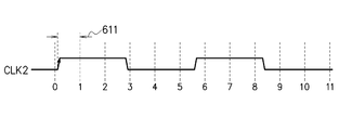
- the quantization error 611 in FIG. 6B is larger than the quantization error 601 in FIG. 6B, which degrades the performance.
- the number of phases of the output clock signals ⁇ 1 to ⁇ p cannot be arbitrarily set because the resolution, power consumption, and area are in a trade-off relationship.
- the delay time of the delay element 311 and the like depends on the process, temperature, and / or voltage, the number of phases locked by the phase lock loop circuit varies depending on conditions.
- FIG. 7A is a diagram illustrating an example in which 16-phase clock signals ⁇ 1 to ⁇ 16 are generated
- FIG. 7B is a diagram illustrating an example in which 18-phase clock signals ⁇ 1 to ⁇ 18 are generated.
- the precision is B bits
- the number of stages of the delay elements 311 and the like is 2 B. Therefore, when the precision is increased, the number of stages of the delay elements 311 and the like increases rapidly. In this case, if the resolution is increased by 1 bit, the number of stages of the delay elements 311 and the like is doubled. Both power consumption and area are doubled. Moreover, in order to normalize, a divider is required, and an area and power consumption increase. Next, a multiphase clock generation circuit for solving the above problem will be described.
- FIG. 8A is a diagram showing a configuration example of a multiphase clock generation circuit using a two-stage time digital converter
- FIG. 8B is a diagram for explaining the operation.
- the time digital converter has two stages of a coarse time digital converter 801 and a fine time digital converter 803.
- the coarse time digital converter 801 has the same configuration as that in FIG. 3B, and the delay time of the delay elements 311 to 313 and the like is relatively long. Therefore, the oscillation clock signal is low resolution with a large unit delay amount “1”. A period 823 of 521 is detected.
- the stage (pulse generator and delay compensator) 802 is provided between the coarse time digital converter 801 and the fine time digital converter 803.
- the delay circuit 804 delays the oscillation clock signal CLK ⁇ b> 2 by the same time as the delay time of the stage 802 and outputs it to the fine time digital converter 803, and the coarse time digital converter 801 and the fine difference time digital converter 803. Compensate the phase between.
- the fine time digital converter 803 has the same configuration as that in FIG. 3B, and the delay time of the delay elements 311 to 313 and the like is relatively short, so that the unit clock delay amount “1” is small and the oscillation clock signal has a high resolution. A phase difference of 822 is detected.
- x corresponds to the unit delay amount “2” of the oscillation clock signal 821
- y corresponds to the unit delay amount “3” of the oscillation clock signal 821.
- the phase between the unit delay amounts “f0” to “f1” corresponds to each delay time of the delay elements 311 to 313 of the fine time digital converter 803.
- “2” is a unit delay amount of the phase difference of the oscillation clock signal 821.
- (10-3) is the unit delay amount of the period 823.
- “F11” is a unit delay amount of the phase difference of the oscillation clock signal 822.
- “F12” is the unit delay amount of the oscillation clock signal 822 corresponding to the unit delay amount “1” of the oscillation clock signal 821.
- the number of delay elements is 2 B1 +2 B2 .
- the number of delay elements increases from 128 to 256 in the circuit of FIG. 3A.
- the area and power consumption are reduced.
- the first problem is that the linearity is degraded due to a delay mismatch between the stage 802 and the delay circuit 804.
- the second problem is that since the normalized value of the coarse time digital converter 801 has only the resolution of the coarse time digital converter 801, the normalized quantization noise is high, and the fine time digital converter 803 has a high resolution. Even if there is a resolution, after normalization, the effective resolution is almost determined by the accuracy of the coarse time digital converter 801.
- a multiphase clock generation circuit for solving the above problem will be described below.
- FIG. 18 is a diagram illustrating a configuration example of the multiphase clock generation circuit according to the first embodiment.
- the counter 306 counts the number of pulses EC of the oscillation clock signal CLK2 existing within one cycle of the reference clock signal CLK1.
- the counter 306 counts the number of pulses EC by counting the number of rising edges of the oscillation clock signal CLK2 existing within one period of the reference clock signal CLK1.
- the number of pulses EC is “8”.
- the time digital converter 1501 receives the reference clock signal CLK1 and the oscillation clock signal CLK2, and generates a plurality of phases of low resolution clock signals ⁇ c1 to ⁇ cp and a plurality of phases of high resolution clock signals ⁇ f1 to ⁇ fp, ⁇ g1 to ⁇ gp.
- FIGS. 9A and 9B are block diagrams showing a configuration example of the time digital converter 1501, and FIG. 9C is a time chart for explaining an operation example thereof.
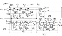
- the time digital converter 1501 includes a first time digital converter 901, a second time digital converter 902, and a third time digital converter 903.
- the first time digital converter 901 is a coarse time digital converter, and includes first delay elements 921 to 928 and the like having a relatively long delay time.
- the buffer 920 amplifies the oscillation clock signal CLK2.
- a series connection circuit such as the first delay elements 921 to 928 is connected to the output terminal of the buffer 920.
- the first delay elements 921 to 928 and the like sequentially delay the oscillation clock signal CLK2.
- Each of the first delay elements 921 to 928 and the like delays the input signal and outputs it.
- the clock signal ⁇ c1 is a signal having the same phase as that of the oscillation clock signal CLK2.
- the clock signal ⁇ c2 is an output signal of the delay element 921.
- Clock signal ⁇ c3 is an output signal of delay element 922.
- Each phase difference of the clock signals ⁇ c1 to ⁇ cp corresponds to each delay time of the first delay elements 921 to 928 and the like.
- Each of the first delay elements 921 to 928 and the like has the same delay time, and the delay time is changed by the delay control signal 914.
- the first time digital converter 901 generates the low-resolution clock signals ⁇ c1 to ⁇ cp of a plurality of phases. As in FIG.
- the D-type flip-flops 931 to 938 and the like latch the values of the clock signals ⁇ c1 to ⁇ cp at the time 420 of the rising edge of the reference clock signal CLK1, and store the binary first digital value 911 as Q Output from the terminal.
- the first time digital converter 901 uses the plurality of first delay elements 921 to 928 to delay the oscillation clock signal CLK2 relative to the reference clock signal CLK1 to thereby make a plurality of phases.
- First clock signals ⁇ c1 to ⁇ cp are generated, and the values of the first clock signals ⁇ c1 to ⁇ cp of a plurality of phases at the edge time 420 of the reference clock signal CLK1 are output as the first digital value 911.
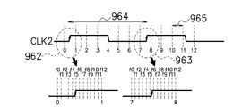
- the unit delay amount 965 of the oscillation clock signal CLK2 is variable as shown in FIG. 9C.
- the phase between the unit delay amounts “0” to “1” of the oscillation clock signal CLK 2 corresponds to the delay time of the first delay element 921.
- the second time digital converter 902 is a fine time digital converter, and includes second delay elements 941 to 943 having a delay time shorter than that of the first delay elements 921 to 928 and the like.
- a series connection circuit such as the second delay elements 941 to 943 is connected to the output terminal of the buffer 920.
- the second delay elements 941 to 943 and the like sequentially delay the oscillation clock signal CLK2.
- the second delay elements 941 to 943 and the like delay the input signal and output it.
- the clock signal ⁇ f1 is a signal having the same phase as that of the oscillation clock signal CLK2.
- Clock signal ⁇ f2 is an output signal of delay element 941.
- Clock signal ⁇ f3 is an output signal of delay element 942.
- Each phase difference of the clock signals ⁇ f1 to ⁇ fp corresponds to each delay time of the second delay elements 941 to 943 and the like.
- Each of the second delay elements 941 to 943 has the same delay time.
- the second time digital converter 902 generates the multi-phase high resolution clock signals ⁇ f1 to ⁇ fp.
- the D-type flip-flops 951 to 953 and the like latch the values of the clock signals ⁇ f1 to ⁇ fp at the time 420 of the rising edge of the reference clock signal CLK1, and store the binary second digital value 912 as Q Output from the terminal.
- the second time digital converter 902 uses the plurality of second delay elements 941 to 943 and the like having a delay time shorter than the delay times of the first delay elements 921 to 928 and the like. Are delayed relative to the reference clock signal CLK1 to generate second clock signals ⁇ f1 to ⁇ fp of a plurality of phases, and second clock signals ⁇ f1 to ⁇ fp of a plurality of phases at the edge time 420 of the reference clock signal CLK1. Is output as the second digital value 912. As shown in FIG. 9C, the second time digital converter 902 is a circuit for detecting the phase of the first rising edge 962 of the oscillation clock signal CLK2. The phase between the unit delay amounts “f0” to “f1” of the oscillation clock signal CLK2 corresponds to the delay time of the second delay element 941.
- the third time digital converter 903 is a fine time digital converter similar to the second time digital converter 902, and third delay elements 981 to 981 having the same delay time as the second delay elements 941 to 943 and the like. 983 etc.
- the serial connection circuits such as the third delay elements 981 to 983 are connected to the output terminal of the first delay element 927 (the input terminal of the first delay element 928).
- the third delay elements 981 to 983 and the like sequentially delay the first clock signal ⁇ c8 output from the first delay element 927.
- the third delay elements 981 to 983 and the like delay the input signal and output it.
- the clock signal ⁇ g1 is the same signal as the first clock signal ⁇ c8 output from the first delay element 927.
- the clock signal ⁇ g2 is an output signal of the delay element 981.
- Clock signal ⁇ g3 is an output signal of delay element 982.
- Each phase difference of the clock signals ⁇ g1 to ⁇ gp corresponds to each delay time of the third delay elements 981 to 983 and the like.
- Each of the third delay elements 981 to 983 has the same delay time. In this way, the third time digital converter 903 generates a plurality of phases of high resolution clock signals ⁇ g1 to ⁇ gp. As in FIG.
- the D-type flip-flops 991 to 993 and the like latch the values of the clock signals ⁇ g1 to ⁇ gp at the time 420 of the rising edge of the reference clock signal CLK1, and store the binary third digital value 913 as Q Output from the terminal.
- the third time digital converter 903 uses a plurality of third delay elements 981 to 983 and the like having the same delay time as the second delay elements 941 to 943 and the like.
- the first clock signals ⁇ c8 delayed by the one delay elements 921 to 927 are delayed to generate the third clock signals ⁇ g1 to ⁇ gp of the plurality of phases, and the first of the plurality of phases at the edge time of the reference clock signal CLK1. 3 are output as third digital values 913.
- the third time digital converter 903 is a circuit for detecting the phase of the second rising edge 963 of the oscillation clock signal CLK2.
- the phase between the unit delay amounts “f0” to “f1” of the oscillation clock signal CLK2 corresponds to the delay time of the third delay element 981.
- the calibration circuit 904 in FIG. 9A includes the decoder 302, the subtractor 1504, the second low-pass filter 1505, and the adder 303 in FIG.
- the calibration circuit 904 includes a first digital value 911 of the first time digital converter 901, a second digital value 912 of the second time digital converter 902, and a third digital value of the third time digital converter 903.
- the digital value 913 is input, and the period 964 of the oscillation clock signal CLK2 is calculated in the same manner as in the method of FIGS.
- the period 964 is output to the first low-pass filter 304 in FIG.
- the first time digital converter 901 is a circuit for detecting the rising edges 962 and 963 of the oscillation clock signal CLK2 with low resolution.
- the rising edge 962 is detected as a unit delay amount “1”
- the rising edge 963 is detected as a unit delay amount “8”.
- the second time digital converter 902 is a circuit for detecting the first rising edge 962 of the oscillation clock signal CLK2 with high resolution.
- the rising edge 962 is detected as the unit delay amount “f5”.
- the third time digital converter 903 is a circuit for detecting the second rising edge 963 of the oscillation clock signal CLK2 with high resolution.
- the rising edge 963 is detected as the unit delay amount “f6”.
- the decoder 302 and the adder 303 are based on the count number EC of the counter 306 and the first to third digital values 911 to 913 according to the above equation (1) after normalization, as in FIG. Then, the cycle Tref of the reference clock signal CLK1 is calculated.
- the adder 303 outputs the cycle Tref of the reference clock signal CLK1 to the first low-pass filter 304.
- the first low-pass filter 304 is connected to the input terminal of the oscillator 305 and averages and outputs the period Tref of the reference clock signal CLK1 by digital low-pass filtering.
- the oscillator 305 Based on the period Tref of the reference clock signal CLK1 output from the first low-pass filter 304, the oscillator 305 generates an oscillation clock signal CLK2 having a period of 1 / m (m is an integer of 2 or more) of the period Tref of the reference clock signal CLK1. And is fed back to the counter 306 and the time digital converter 1501.
- This feedback circuit is a phase-locked loop circuit.
- the phase difference between the oscillation clock signal CLK2 and the reference clock signal CLK1 approaches 0, and the phase difference converges around 0. That is, for example, the clock signal ⁇ c1 is locked in synchronization with the phase of the reference clock signal CLK1.
- the multiphase clock generation circuit can output a plurality of phase clock signals ⁇ c1 to ⁇ cp synchronized with the phase of the reference clock signal CLK1.
- the time digital converter 1501, the decoder 302, the adder 303, the first low-pass filter 304, the subtractor 1504, and the second low-pass filter 1505 in the subsequent stage can be configured by digital circuits.
- the clock generation circuit can be downsized and power consumption can be reduced.
- the calibration circuit 904 in FIG. 9A outputs a delay control signal 914 to the first delay elements 921 to 928 of the first digital converter 901.
- the delay time of the first delay elements 921 to 928 and the like changes according to the delay control signal 914.
- FIG. 10A is a diagram illustrating a configuration example of each of the variable delay elements 921 to 928 and the like in FIG. 9B.
- the delay element 1001 is connected to the variable current source 1002, delays the signal at the input terminal IN, and outputs it to the output terminal OUT.
- the control terminal CON1 receives the analog delay control signal 914 in FIG. 9B and controls the current flowing through the variable current source 1002.
- the delay time of the delay element 1001 is shortened, and when the current of the variable current source 1002 is small, the delay time of the delay element 1001 is lengthened.
- FIG. 10B is a diagram showing another configuration example of each of the variable delay elements 921 to 928 and the like shown in FIG. 9B.
- the delay element 1001 includes a plurality of series connection circuits of a current source 1011 and a switch 1012 connected in parallel, delays a signal at the input terminal IN, and outputs the signal to the output terminal OUT.
- the control terminal CON2 inputs the digital delay control signal 914 shown in FIG. 9B and controls on / off of the plurality of switches 1012. If the total current flowing through the plurality of current sources 1011 is large, the delay time of the delay element 1001 is shortened. If the total current flowing through the plurality of current sources 1011 is small, the delay time of the delay element 1001 is increased.
- FIG. 10C is a diagram showing another configuration example of each of the variable delay elements 921 to 928 and the like in FIG. 9B.
- the delay element 1001 is connected to the variable capacitor 1021, delays the signal of the input terminal IN, and outputs it to the output terminal OUT.
- the control terminal CON3 inputs the analog delay control signal 914 shown in FIG. 9B and controls the capacitance value of the variable capacitor 1021. If the capacitance value of the variable capacitor 1021 is small, the delay time of the delay element 1001 is shortened, and if the capacitance value of the variable capacitor 1021 is large, the delay time of the delay element 1001 is lengthened.
- FIG. 10D is a diagram showing another configuration example of each of the variable delay elements 921 to 928 and the like in FIG. 9B.
- the delay element 1001 includes a plurality of series connection circuits of a capacitor 1031 and a switch 1032 connected in parallel, delays the signal of the input terminal IN, and outputs the signal to the output terminal OUT.
- the control terminal CON4 receives the digital delay control signal 914 shown in FIG. 9B and controls on / off of the plurality of switches 1032. If the capacitance value connected to the delay element 1001 is small, the delay time of the delay element 1001 is shortened, and if the capacitance value connected to the delay element 1001 is large, the delay time of the delay element 1001 is lengthened.
- FIG. 11A and 11B are diagrams for explaining the delay time control of the calibration circuit 904 in FIG. 9A.
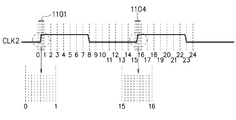
- FIG. 11A is a time chart showing a state before the phase-locked loop circuit is locked.
- the horizontal axis indicates the unit delay amount of the first time digital converter 901.
- a region 1101 is a region between unit delay amounts “0” to “1”, and is a region having a high-resolution unit delay amount of the second time digital converter 902.
- a region 1104 is a region between unit delay amounts “15” to “16”, and has a high resolution unit delay amount of the third time digital converter 903.
- the rising edge of the oscillation clock signal CLK2 has a phase difference 1102 with respect to the rising edge of the reference clock signal CLK1.
- FIG. 11B is a time chart showing a state after the phase lock loop circuit is locked and before calibration.
- the phase lock loop circuit reduces the phase difference of the oscillation clock signal CLK2 with respect to the reference clock signal CLK1.
- the phase difference 1103 of the oscillation clock signal CLK2 with respect to the reference clock signal CLK1 becomes substantially zero.
- the second time digital converter 902 operates in a region 1101 where the unit delay amount is between “0” and “1”
- the third time digital converter 903 has unit delay amounts of “15” to “1”. 16 "operates in the region 1104.
- the oscillation clock signal CLK2 is divided into 16 by the delay element, so that Clock signals ⁇ c1 to ⁇ c16 can be generated.
- the second rising edge of the oscillation clock signal CLK2 is located between unit delay amounts “13” to “14”. In this state, the 14-phase first clock signals ⁇ c1 to ⁇ c14 are generated, and the desired 16 phases cannot be obtained.
- the delay time of the first delay elements 921 to 928 and the like dynamically varies depending on the process, temperature, and / or voltage.
- the number of phases of the first clock signals ⁇ c1 to ⁇ cp can also change dynamically. Therefore, stable 16-phase first clock control signals ⁇ c1 to ⁇ c16 can be generated by the delay time control of the calibration circuit 904 in FIG. 9A.
- the phase information of the second rising edge of the oscillation clock signal CLK2 becomes the period information of the oscillation clock signal CLK2.
- the decoder 302 in FIG. 18 outputs the phase information of the second rising edge of the oscillation clock signal CLK2 to the subtractor 1504 as the period information of the oscillation clock signal CLK2.
- the period of the oscillation clock signal CLK2 is the unit delay amount “14”.
- the subtractor 1504 outputs the difference between the period (for example, “14”) detected by the decoder 302 and the target period (target phase number) RD (for example, “16”) to the second low-pass filter 1505.
- the subtractor 1504 outputs a difference between the period of the oscillation clock signal CLK2 obtained based on at least the first digital value 911 and the third digital value 913 and the target period RD.
- the second low-pass filter 1505 is connected between the subtractor 1504 and the first time digital converter 901, and the output signal of the subtractor 1504 is averaged by performing digital low-pass filtering on the output signal of the subtractor 1504.
- the signal is output as a delay control signal 914 to the first delay elements 921 to 928 in the first time digital converter 901.
- the subtractor 1504 and the second low-pass filter 1505 constitute a delay control unit. For example, in FIG.
- the oscillation clock signal CLK2 has a period of “14” and is shorter than the target period RD (eg, “16”), so the delay time of the first delay elements 921 to 928 and the like is shortened.
- the lengths of the areas 1101 and 1104 correspond to the delay times of the first delay elements 921 to 928 and the like.
- the oscillation clock signal CLK2 has a first rising edge located in the area 1101 and a second rising edge located in the area 1104. As a result, the oscillation clock signal CLK2 can be divided into 16 and 16-phase first clock signals ⁇ c1 to ⁇ c16 are generated. By this calibration feedback loop processing, the oscillation clock signal CLK 2 is locked such that the first rising edge is located in the area 1101 and the second rising edge is located in the area 1104. As a result, the number of phases of the first clock signals ⁇ c1 to ⁇ cp is locked to “16”.
- the second time digital converter 902 performs the first time of the oscillation clock signal CLK2.
- the phase of the rising edge can be detected.
- the third time digital converter 903 performs the phase of the second rising edge of the oscillation clock signal CLK2. Can be detected.
- the stage 802 in FIG. 8A is not necessary, and only two fine time digital converters 902 and 903 corresponding to the regions 1101 and 1104 may be provided. There is no need to provide a fine time digital converter.
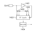
- FIG. 14A is a diagram showing a configuration example of a circuit for normalizing the fine time digital converters 902 and 903 to the coarse time digital converter 901.
- the method of calculating the phase difference using the fine digital converter 803 and the coarse time digital converter 801 has been described above with reference to FIG. In the present embodiment, similarly, the phase difference is calculated using the fine digital converters 902 and 903 and the coarse time digital converter 901.
- One first delay element 1401 is any one of the first delay elements 921 to 928 in FIG. 9B.
- the plurality of second delay elements 1402 correspond to the second delay elements 941 to 943 in FIG. 9B.
- the first delay element 1401 delays and outputs the reference clock signal CLK1.
- the series connection circuit of the plurality of second delay elements 1402 delays and outputs the reference clock signal CLK1, for example.
- the flip-flop bank 1403 has a plurality of flip-flops, and in synchronization with, for example, the rising edge of the output signal of the first delay element 1401, latches the output signals of the plurality of second delay elements 1402 and outputs them to the decoder 1404. To do.
- the decoder 1404 can detect how many delay times of the second delay element 1401 are the delay time of the first delay element 1401. That is, it is possible to detect how many unit delay amounts of the second time digital converter 902 is the magnitude of the unit delay amount “1” of the first time digital converter 901.
- the decoder 302 can perform normalization and detect the phase of the first rising edge and the second rising edge of the oscillation clock signal CLK2 as in FIG. 8B.
- the second digital converter 902 has been described above as an example, the same applies to the third time digital converter 903.
- FIG. 14B is a diagram illustrating another configuration example of a circuit for normalizing the fine time digital converters 902 and 903 to the coarse time digital converter 901.
- the circuit in FIG. 14B is obtained by adding a low-pass filter 1411 to the circuit in FIG. 14A.
- the second delay element 1412 is a variable delay element provided in place of the second delay element 1402.
- the decoder 1404 detects how many second delay elements 1412 the delay time of the first delay element 1401 is, and outputs the difference between the number and the target number to the low-pass filter 1411.
- the low pass filter 1411 averages the output of the decoder 1404 by low pass filtering, and outputs a delay control signal to the plurality of second delay elements 1412.
- the delay times of the plurality of second delay elements 1412 change according to the delay control signal.
- the difference output from the decoder 1404 converges to 0.
- the decoder 302 in FIG. 18 performs normalization using the target number, and can detect the phase of the first rising edge and the second rising edge of the oscillation clock signal CLK2.
- the multiphase clock generation circuit in FIG. 18 directly connects the coarse time digital converter 901 to the fine time digital converters 902 and 903 without passing through the stage 802 in FIG. 8A. This connection eliminates delay mismatch due to the stage 802 and improves the linearity of the characteristics.
- the number of delay elements is 2 B1 +2 B2 + 1 .
- the time digital converter 1501 the subsequent stage decoder 302, adder 303, first low-pass filter 304, subtractor 1504, and second low-pass filter 1505 can be configured with digital circuits.
- the multiphase clock generation circuit can be reduced in size and power consumption can be reduced.
- the normalization process is simplified, so the number of bits required for normalization is reduced, and the multiphase clock generation circuit reduces the circuit scale area and power consumption. To do.
- FIG. 15A is a diagram illustrating a configuration example of a multiphase clock generation circuit according to the second embodiment.
- the circuit in FIG. 15A is obtained by adding an offset lock detector 1503 and an adder 1502 to the circuit in FIG.
- the offset lock detector 1503 outputs the offset phase to the adder 1502 when detecting the offset lock based on the output signal of the decoder 302.
- Adder 1502 adds the offset phase to the output signal of decoder 302 and outputs the result to adder 303. Details of the operation will be described below.
- FIG. 15B is a diagram for explaining the offset lock.
- the phase-locked loop circuit is locked with the frequency clock signal CLK2 having an offset phase.
- the first rising edge is located in a region between unit delay amounts “1” and “2”
- the second rising edge is unit delay amounts “16” and “17”. It is locked in a state located in the area between. In this state, the second time digital converter 902 and the third time digital converter 903 cannot detect the rising edge of the oscillation clock signal CLK2. Calibration is required to remove this offset phase.
- the offset lock detector 1503 is such that the first rising edge of the oscillation clock signal CLK2 is not located in the area 1101 and the second rising edge of the oscillation clock signal CLK2 is in the area 1104 in a state where the phase lock loop circuit is locked. When it is not positioned at the position, it is determined that there is an offset phase, and the offset phase is output to the adder 1502. Adder 1502 adds the offset phase to the output signal of decoder 302 and outputs the result to adder 303. That is, the offset lock detector 1503 and the adder 1502 are input to the oscillator 305 when the second digital value 912 and the third digital value 913 are locked in a state where the edge of the oscillation clock signal CLK2 does not exist.
- An offset phase is added to the period.
- the offset phase is removed, and the oscillation clock signal CLK2 is corrected so that the first rising edge is located in the area 1101 and the second rising edge is located in the area 1104.
- the oscillation clock signal CLK2 is corrected so that the first rising edge is located in the area 1101 and the second rising edge is located in the area 1104.
- FIG. 17A is a diagram illustrating a configuration example of a multiphase clock generation circuit according to the third embodiment.
- the circuit of FIG. 17A is obtained by providing a variable delay circuit 1701 instead of the adder 1502 with respect to the circuit of FIG. 15A.
- the offset lock detector 1503 When detecting the offset lock, the offset lock detector 1503 outputs a delay control signal corresponding to the offset phase to the variable delay circuit 1701.
- the variable delay circuit 1701 delays the oscillation clock signal CLK2 output from the oscillator 305 by a delay time corresponding to the delay control signal, and outputs the delayed clock signal CLK2 to the counter 306 and the time digital converter 1501. Details of the operation will be described below.
- FIGS. 16A and 16B are diagrams showing examples of convergence of the locked state of the phase-locked loop circuit.
- the phase lock loop circuit converges while oscillating when the phase difference of the oscillation clock signal CLK2 is near zero.
- the first rising edge of the oscillation clock signal CLK2 shifts to the plus side of the unit delay amount “0” as shown in FIG. 16A and the minus side of the unit delay amount “0” as shown in FIG. 16B.
- the oscillation clock signal CLK2 operates normally because the first rising edge is located in the area 1101 and the second rising edge is located in the area 1104.
- the oscillation clock signal CLK2 has the first rising edge not located in the area 1101 and the second rising edge is not located in the area 1104. Therefore, the fine time digital converter 902 And 903 cannot detect the rising edge of the oscillation clock signal CLK2.
- the counter 306 is used and the phase difference becomes negative as shown in FIG. 16B, the first rising edge of the oscillation clock signal CLK2 is detected between the unit delay amounts “14” and “15”.
- an offset phase can be added by the circuit of FIG. 15A.
- the circuit of FIG. 17A by providing the variable delay circuit 1701, as shown in FIG. 17B, the unit delay amount on the horizontal axis is shifted to the right, and the unit delay amount is started from “ ⁇ 1”. Can do.
- the offset lock detector 1503 is such that the first rising edge of the oscillation clock signal CLK2 is not located in the area 1101 and the second rising edge of the oscillation clock signal CLK2 is in the area 1104 in a state where the phase lock loop circuit is locked. When it is not located at the position, it is determined that an offset phase exists, and a delay control signal corresponding to the offset phase is output to the variable delay circuit 1701.
- the variable delay circuit 1701 delays the oscillation clock signal CLK2 output from the oscillator 305 by a delay time corresponding to the delay control signal, and outputs the delayed clock signal CLK2 to the counter 306 and the time digital converter 1501.
- the oscillator 305 An offset phase is given to the oscillation clock signal CLK2 to be output.
- the oscillation clock signal CLK2 is corrected so that the first rising edge is located in the area 1101 and the second rising edge is located in the area 1104. Is possible.
- FIG. 19 is a diagram illustrating a configuration example of a multiphase clock generation circuit according to the fourth embodiment.
- the circuit of FIG. 19 is obtained by adding a digital-analog converter 1901 and an analog low-pass filter 1902 to the circuit of FIG.
- the digital-analog converter 1901 converts the delay control signal output from the second low-pass filter 1505 from digital to analog.
- the low-pass filter 1902 averages the analog delay control signal by low-pass filtering and outputs the averaged signal to the first delay elements 921 to 928 in the first time digital converter 901.
- the first delay elements 921 to 928 vary in delay time according to an analog delay control signal.
- the first delay elements 921 to 928 can be analog controlled by the configuration of FIG. 10A or 10C.
- the delay control of the first time digital converter 901 is simplified.
- the low-pass filter 1902 may be deleted. By providing the low pass filter 1902, the delay control signal is stabilized and noise is reduced.
- FIG. 20 is a diagram illustrating a configuration example of a multiphase clock generation circuit according to the fifth embodiment.
- the circuit of FIG. 20 is obtained by providing a successive approximation register (SAR) engine 2001 in place of the subtractor 1504 and the second low-pass filter 1505 with respect to the circuit of FIG.
- SAR successive approximation register
- the successive approximation register engine 2001 sequentially compares the cycle of the oscillation clock signal CLK2 obtained based on at least the first digital value 911 and the third digital value 913 of FIG. 9B and the target cycle RD in order from the upper bit.
- the delay control unit determines the delay control signal in order from the higher order bits and outputs it to the first delay elements 921 to 928 in the first time digital converter 901.
- the successive approximation register engine 2001 calculates the difference between the cycle of the oscillation clock signal CLK2 output from the decoder 302 and the target cycle RD in order from the upper bit, and outputs the delay control signals from the first delay elements 921 to 928 and the like in order from the upper bit. Change one bit at a time. By comparing before and after the delay time of the first delay elements 921 to 928 etc. is changed, it is determined whether or not the error is reduced when the bit of the delay control signal is changed, and the same applies to the next bit. Repeat this and calibrate bit by bit.
- the processing of the successive approximation register engine 2001 is simple, the circuit scale and power consumption are reduced, and convergence is accelerated.
- the successive approximation register engine 2001 is stopped after calibrating all the bits, there is a possibility that the period value of the oscillation clock signal CLK2 output from the decoder 302 may change due to fluctuations in temperature or voltage. Therefore, it is necessary to detect whether the cycle of the oscillation clock signal CLK2 output from the decoder 302 is positive without stopping the successive approximation register engine 2001 even after all bits have been calibrated. If the cycle is not correct, it is necessary to change the value of the delay control signal and match the cycle of the oscillation clock signal CLK2. In this case, since the fluctuation of the cycle of the oscillation clock signal CLK2 is small, only the lower bits of the delay control signal need be changed.
- FIG. 21 is a diagram illustrating a configuration example of a multiphase clock generation circuit according to the sixth embodiment.
- the circuit of FIG. 21 is obtained by adding a frequency divider 2201 to the circuit of FIG.
- the oscillator 305 is a multi-phase oscillation clock signal having a period of 1 / m (m is an integer of 2 or more) of the period of the reference clock signal CLK1, based on the period of the reference clock signal CLK1 output from the first low-pass filter 304. ⁇ 1 to ⁇ p are generated.
- the oscillator 305 is 1 / m (m of the period of the reference clock signal CLK1 based on the period of the reference clock signal CLK1 obtained based on the count number of the counter 306 and the first to third digital values 911 to 913.
- the frequency divider 2201 divides one oscillation clock signal (for example, the oscillation clock signal ⁇ 1) among the oscillation clock signals ⁇ 1 to ⁇ p of the plurality of phases, and the counter 306, the first time digital converter 901, and the second Output to the time digital converter 902.
- the frequency divider 2201 outputs a clock signal having a frequency lower than that of the oscillation clock signals ⁇ 1 to ⁇ p.
- the first clock signals ⁇ c1 to ⁇ cp have the same frequency as the output clock signal of the frequency divider 2201.
- the multiple-phase first clock signals ⁇ c1 to ⁇ cp have a frequency of 1 / m lower than the multiple-phase oscillation clock signals ⁇ 1 to ⁇ p.
- the multiphase clock generation circuit of the present embodiment can output the low-frequency multiple-phase first clock signals ⁇ c1 to ⁇ cp and the high-frequency multiple-phase oscillation clock signals ⁇ 1 to ⁇ p to the outside.
- the frequency of the first clock signals ⁇ c1 to ⁇ cp is 100 MHz, and the frequency of the oscillation clock signals ⁇ 1 to ⁇ p is 1 GHz.
- clock signals ⁇ c1 to ⁇ cp and clock signals ⁇ 1 to ⁇ p having two types of frequencies can be generated.
- the multiphase clock generation circuit has a small area and low power consumption. Power is reduced, noise is reduced, and performance is improved.
- the accuracy of the time digital converter 1501 is increased by 2 bits, the quantization noise is reduced to a quarter.
- the coarse time digital converter 901 and the fine time digital converters 902 and 903 the number of delay elements can be reduced and the size and size can be reduced as compared with the case where the single stage time digital converter 301 is used as shown in FIG. 3A. Low power consumption can be achieved.
- the multiphase clock generation circuit of the above embodiment can be used for a wireless communication circuit, a processor, an analog-digital converter, a clock data recovery system, or the like.
- the first time digital converter can output a first clock signal having a plurality of phases.
- digital processing becomes possible, so that a highly accurate and / or small clock generation circuit can be provided.
Landscapes
- Physics & Mathematics (AREA)
- Nonlinear Science (AREA)
- Manipulation Of Pulses (AREA)
- Analogue/Digital Conversion (AREA)
- Stabilization Of Oscillater, Synchronisation, Frequency Synthesizers (AREA)
- Pulse Circuits (AREA)
Abstract
基準クロック信号の1周期内に存在する発振クロック信号のパルス数をカウントするカウンタ(306)と、発振クロック信号を遅延させることにより複数相の第1のクロック信号を生成する第1の時間デジタル変換器(1501)と、短い遅延時間で発振クロック信号を遅延させることにより複数相の第2のクロック信号を生成する第2の時間デジタル変換器(1501)と、遅延させられた第1のクロック信号を遅延させることにより複数相の第3のクロック信号を生成する第3の時間デジタル変換器(1501)と、発振クロック信号の周期と目標周期との差分を基に遅延制御信号を出力する遅延制御部(1504)と、基準クロック信号の周期を基に、基準クロック信号の周期の1/mの周期の発振クロック信号を生成する発振器(305)とを有し、第1の時間デジタル変換器内の遅延素子は、遅延制御信号に応じて遅延時間が変化するクロック生成回路が提供される。
Description
本発明は、クロック生成回路に関する。
図1は、多相クロック生成回路の構成例を示す図である。多相クロック生成回路は、位相周波数検出器101、ローパスフィルタ102、発振器103及び分周器104を含む位相ロックループ(PLL:phase-locked loop)回路を有する。位相周波数検出器101は、分周器104の出力クロック信号と基準クロック信号CLKとの間で位相及び周波数を比較し、その位相の差分を出力する。ローパスフィルタ102は、位相周波数検出器101が出力する位相の差分を平均化して出力する。発振器103は、その差分の平均値が小さくなるように位相調整された複数相のクロック信号φ1~φpを生成して出力する。分周器104は、例えばクロック信号φ1を分周し、クロック信号φ1より周波数が低いクロック信号を位相周波数検出器101にフィードバック出力する。このフィードバックループ処理により、クロック信号φ1は、基準クロック信号CLKと同じ位相にやがて収束してロックする。
図1の多相クロック生成回路は、システムが簡単であり、消費電力が小さい利点がある。しかし、図1の多相クロック生成回路は、発振器103がリング発振器であるため、ノイズ特性が低下し、高い周波数で発振できない欠点がある。また、図1の多相クロック生成回路は、ノイズと周波数の問題を解決するため、複数のインダクタを利用して発振器103を作ることが可能だが、面積が膨大になり、コストが高くなる欠点がある。
図2は、他の多相クロック生成回路の構成例を示す図である。図2の多相クロック生成回路は、図1の多相クロック生成回路に対して、遅延線201、位相検出器202及びローパスフィルタ203を追加したものである。遅延線201、位相検出器202及びローパスフィルタ203は、遅延ロックループ(DLL:delay-locked loop)回路を構成する。ここで、発振器103は、単相のクロック信号を分周器104、遅延線201及び位相検出器202に出力する。遅延線201は、発振器103の出力クロック信号を遅延させることにより複数相のクロック信号φ1~φpを出力する。位相検出器202は、発振器103の出力クロック信号及び例えばクロック信号φ1の位相を比較し、その位相の差分をローパスフィルタ203に出力する。ローパスフィルタ203は、その位相の差分を平均化し、遅延線201に出力する。遅延線201は、ローパスフィルタ203が出力する位相の差分が小さくなるように位相調整された複数相のクロック信号φ1~φpを生成して出力する。この遅延ロックループ回路の処理により、クロック信号φ1は、基準クロック信号CLKと同じ位相にやがて収束してロックする。
図2の多相クロック生成回路は、1つのインダクタを用いて発振器103を構成することにより、位相ロックループ回路のノイズ特性を改善することができる利点がある。しかし、図2の多相クロック生成回路は、2個のローパスフィルタ102及び203が必要になり、回路面積が膨大になる欠点がある。
また、粗時間変換装置、第1微細時間レジスタ及び第2微細時間レジスタを有し、粗時間変換と微細時間変換を組み合わせた時間デジタル変換器が知られている(例えば、特許文献1及び特許文献2参照)。
本発明の目的は、複数相のクロック信号を生成することができる高精度及び/又は小型のクロック生成回路を提供することである。
クロック生成回路は、基準クロック信号の1周期内に存在する発振クロック信号のパルス数をカウントするカウンタと、複数の第1の遅延素子を用いて前記発振クロック信号を前記基準クロック信号に対して相対的に遅延させることにより複数相の第1のクロック信号を生成し、前記基準クロック信号のエッジ時点における前記複数相の第1のクロック信号の値を第1のデジタル値として出力する第1の時間デジタル変換器と、前記第1の遅延素子の遅延時間より短い遅延時間の複数の第2の遅延素子を用いて前記発振クロック信号を前記基準クロック信号に対して相対的に遅延させることにより複数相の第2のクロック信号を生成し、前記基準クロック信号のエッジ時点における前記複数相の第2のクロック信号の値を第2のデジタル値として出力する第2の時間デジタル変換器と、前記第2の遅延素子の遅延時間と同じ遅延時間の複数の第3の遅延素子を用いて、前記複数の第1の遅延素子により遅延させられた前記第1のクロック信号を前記基準クロック信号に対して相対的に遅延させることにより複数相の第3のクロック信号を生成し、前記基準クロック信号のエッジ時点における前記複数相の第3のクロック信号の値を第3のデジタル値として出力する第3の時間デジタル変換器と、少なくとも前記第1のデジタル値及び前記第3のデジタル値を基に得られる前記発振クロック信号の周期と目標周期との差分を基に遅延制御信号を出力する遅延制御部と、前記カウンタのカウント数及び前記第1~第3のデジタル値を基に得られる前記基準クロック信号の周期を基に、前記基準クロック信号の周期の1/m(mは2以上の整数)の周期の前記発振クロック信号を生成する発振器とを有し、前記第1の時間デジタル変換器内の前記複数の第1の遅延素子は、前記遅延制御部により出力される前記遅延制御信号に応じて遅延時間が変化し、前記第1の時間デジタル変換器は、前記複数相の第1のクロック信号を出力する。
第1の時間デジタル変換器は、複数相の第1のクロック信号を出力することができる。第1~第3の時間デジタル変換器を設けることにより、デジタル処理が可能になるため、高精度及び/又は小型のクロック生成回路を提供することができる。
(第1の実施形態)
図3Aはデジタル位相ロックループ回路を用いた多相クロック生成回路の構成例を示す図であり、図5は多相クロック生成回路の動作例を説明するためのタイミングチャートである。カウンタ306は、基準クロック信号CLK1の1周期内に存在する発振クロック信号CLK2のパルス数ECをカウントする。例えば、カウンタ306は、基準クロック信号CLK1の1周期内に存在する発振クロック信号CLK2の立ち上がりエッジ数をカウントすることにより、パルス数ECをカウントする。例えば、図5の場合、パルス数ECは「8」である。時間デジタル変換器(TDC)301は、基準クロック信号CLK1及び発振クロック信号CLK2を入力し、複数相のクロック信号φβ1~φβpを生成する。
図3Aはデジタル位相ロックループ回路を用いた多相クロック生成回路の構成例を示す図であり、図5は多相クロック生成回路の動作例を説明するためのタイミングチャートである。カウンタ306は、基準クロック信号CLK1の1周期内に存在する発振クロック信号CLK2のパルス数ECをカウントする。例えば、カウンタ306は、基準クロック信号CLK1の1周期内に存在する発振クロック信号CLK2の立ち上がりエッジ数をカウントすることにより、パルス数ECをカウントする。例えば、図5の場合、パルス数ECは「8」である。時間デジタル変換器(TDC)301は、基準クロック信号CLK1及び発振クロック信号CLK2を入力し、複数相のクロック信号φβ1~φβpを生成する。
図3Bは図3Aの時間デジタル変換器301の構成例を示す図であり、図4は多相クロック信号φβ1~φβpの例を示すタイミングチャートである。ここでは、pが12の例を示す。複数の遅延素子311~313等の直列接続回路は、発振クロック信号CLK2を順次遅延させる。遅延素子311~313等は、それぞれ、入力信号を遅延させて出力する。クロック信号φβ1は、発振クロック信号CLK2と同じ信号である。クロック信号φβ2は、遅延素子311の出力信号である。クロック信号φβ3は、遅延素子312の出力信号である。クロック信号φβ1~φβ12の各位相差は、遅延素子311~313等の各遅延時間に対応する。遅延素子311~313等の各々は、遅延時間が同じである。このようにして、時間デジタル変換器301は、例えば12相のクロック信号φβ1~φβ12を生成することができる。D型フリップフロップ321~323等は、基準クロック信号CLK1の立ち上がりエッジの時点420で、クロック信号φβ1~φβ12の値をラッチし、2値のデジタル値をQ端子から出力する。例えば、D型フリップフロップ321は、基準クロック信号CLK1の立ち上がりエッジの時点420で、クロック信号φβ1の値をラッチし、「1」のデジタル値をQ端子から出力する。これにより、例えば、D型フリップフロップ321~323等のQ端子は、図4に示すように、「111000000111」のデジタル値421を出力する。変化点422は、デジタル値421が「0」から「1」に変化する点である。この変化点422は、発振クロック信号CLK2の基準クロック信号CLK1に対する位相差である。図3Aのデコーダ302が変化点422に対応する位相差を検出する。
図5において、発振クロック信号CLK2は、例えば0~24の単位遅延量の分解能で表すことができる。0~24の単位遅延量は、24個の遅延素子311~313等に対応し、単位遅延量の「1」は、1個の遅延素子の遅延時間に相当する。発振クロック信号CLK2の立ち上がりエッジは、量子化誤差により単位遅延量「3」として検出される。これに対応する位相差PE1は、図4の変化点422の位相差に対応し、発振クロック信号CLK2の基準クロック信号CLK1に対する位相差を表す。このようにして、デコーダ302は、基準クロック信号CLK1の1回目の立ち上がりエッジに対する発振クロック信号CLK2の立ち上がりエッジの位相差PE1を検出し、同様に、基準クロック信号CLK1の2回目の立ち上がりエッジに対する発振クロック信号CLK2の立ち上がりエッジの位相差PE2を検出する。
量子化誤差のため、発振クロック信号CLK2は、1回目の立ち上がりエッジが単位遅延量「3」として検出され、2回目の立ち上がりエッジが単位遅延量「16」として検出される。したがって、発振クロック信号CLK2の周期Tvは、16-3=13の単位遅延量となる。
基準クロック信号CLK1は、タイミングt2の立ち上がりエッジから次のタイミングt2の立ち上がりエッジまでの周期Trefを有する。パルス数ECは、量子化誤差を含み、最大、タイミングt1から次のタイミングt1までの間の発振クロック信号CLK2のパルス数である。
次に、基準クロック信号CLK1の周期Trefの検出方法を説明する。周期Trefは、パルス数EC、位相差PF1及びPF2を基に次式(1)で表される。
Tref=EC-PF1+PF2 ・・・(1)
Tref=EC-PF1+PF2 ・・・(1)
ここで、位相差PF1は、発振クロック信号の周期Tv及び位相差異PE1を基に次式(2)で表される。
PF1=Tv-PE1 ・・・(2)
PF1=Tv-PE1 ・・・(2)
また、位相差PF2は、発振クロック信号の周期Tv及び位相差異PE2を基に次式(3)で表される。
PF2=Tv-PE2 ・・・(3)
PF2=Tv-PE2 ・・・(3)
周期Tvは、上記のように例えば単位遅延量「13」である。また、位相差PE1は、例えば単位遅延量「3」である。位相差PE1を周期Tvの比率に正規化すると、位相差PE1は単位遅延量「3/13」で表される。同様に、位相差PE2の正規化も行われる。デコーダ302及び加算器303は、正規化後に、上式(1)により基準クロック信号CLK1の周期Trefを演算する。加算器303は、基準クロック信号CLK1の周期Trefを第1のローパスフィルタ304に出力する。第1のローパスフィルタ304は、基準クロック信号CLK1の周期Trefをデジタルのローパスフィルタリングにより平均化して出力する。発振器305は、第1のローパスフィルタ304が出力する基準クロック信号CLK1の周期Trefを基に、基準クロック信号CLK1の周期Trefの1/m(mは2以上の整数)の周期の発振クロック信号CLK2を生成し、カウンタ306及び時間デジタル変換器301にフィードバック出力する。このフィードバック回路は、位相ロックループ回路である。発振クロック信号CLK2及び基準クロック信号CLK1の位相差は0に近づき、その位相差は0付近に収束する。すなわち、例えばクロック信号φβ1は、基準クロック信号CLK1の位相に同期した状態でロックする。多相クロック生成回路は、基準クロック信号CLK1の位相に同期した複数相のクロック信号φβ1~φβpを出力することができる。時間デジタル変換器301を用いることにより、その後段のデコーダ302、加算器303及び第1のローパスフィルタ304をデジタル回路で構成することができるので、多相クロック生成回路を小型化し、低消費電力化することができる。
図6Aは単位遅延量が比較的小さい場合の発振クロック信号CLK2の分解能を示す図であり、図6Bは単位遅延量が比較的大きい場合の発振クロック信号CLK2の分解能を示す図である。単位遅延量「1」の大きさは、図3Bの遅延素子311等の遅延時間により決まる。遅延素子311等は、プロセス条件、電圧及び/又は温度に依存して遅延時間が動的に変化する。したがって、図6Aのように単位遅延量「1」の大きさが比較的小さい場合と、図6Bのように単位遅延量「1」の大きさが比較的大きい場合とが存在する。図6A及び図6Bは、同じ発振クロック信号CLK2の基準クロック信号CLK1に対する位相差を検出する様子を示す。図6A及び図6Bの両方において、位相差は単位遅延量「1」として検出される。しかし、図6Bの量子化誤差611は、図6Bの量子化誤差601より大きくなり、性能を劣化させる。分解能を上げた方がよいが、分解能と消費電力、面積はトレードオフの関係にあるため、出力クロック信号φβ1~φβpの相数を任意に設定できない。また、遅延素子311等の遅延時間はプロセス、温度及び/又は電圧に依存するため、位相ロックループ回路でロックされる相数は条件により変わる。
図7Aは16相のクロック信号φβ1~φβ16が生成される例を示す図であり、図7Bは18相のクロック信号φβ1~φβ18が生成される例を示す図である。上記のように、出力クロック信号φβ1~φβpの相数は、条件により変わるため、所望の相数が得られないという課題がある。
また、精度をBビットとすると、遅延素子311等の段数は2Bになるため、精度を上げると遅延素子311等の段数は急激に増える。この場合、分解能を1ビット増やすと、遅延素子311等の段数が2倍増える。消費電力と面積も共に2倍増える。また、正規化するためには、割り算器が必要になり、面積及び消費電力が増大する。次に、上記の課題を解決するための多相クロック生成回路を説明する。
図8Aは2ステージ時間デジタル変換器を用いた多相クロック生成回路の構成例を示す図であり、図8Bはその動作を説明するための図である。時間デジタル変換器は、粗時間デジタル変換器801及び微細時間デジタル変換器803の2ステージを有する。粗時間デジタル変換器801は、図3Bと同様の構成を有し、遅延素子311~313等の遅延時間が比較的長いため、単位遅延量「1」の大きさが大きい低分解能で発振クロック信号521の周期823が検出される。
ステージ(パルス発生器及び遅延補償器)802は、粗時間デジタル変換器801と微細時間デジタル変換器803の間に設けられる。遅延回路804は、発振クロック信号CLK2に対して、ステージ802の遅延時間と同じ時間の遅延を行って微細時間デジタル変換器803に出力し、粗時間デジタル変換器801と微差時間デジタル変換器803との間の位相を補償する。微細時間デジタル変換器803は、図3Bと同様の構成を有し、遅延素子311~313等の遅延時間が比較的短いため、単位遅延量「1」の大きさが小さい高分解能で発振クロック信号822の位相差が検出される。例えば、発振クロック信号822において、xは発振クロック信号821の単位遅延量「2」に対応し、yは発振クロック信号821の単位遅延量「3」に対応する。単位遅延量「f0」~「f1」の間の位相は、微細時間デジタル変換器803の遅延素子311~313等の各遅延時間に相当する。
発振クロック信号821において、周期823は、例えば、10-3=7の単位遅延量である。したがって、発振クロック信号CLK2の基準クロック信号CLK1に対する位相差は、2/(10-3)+(f11/f12)×1/(10-3)で表される。ここで、「2」は、発振クロック信号821の位相差の単位遅延量である。(10-3)は、上記の周期823の単位遅延量である。「f11」は、発振クロック信号822の位相差の単位遅延量である。「f12」は、発振クロック信号821の単位遅延量「1」の大きさに対応する発振クロック信号822の単位遅延量の大きさである。
粗時間デジタル変換器801の精度をB1ビットとし、微細時間デジタル変換器803の精度をB2ビットとすると、遅延素子の数は、2B1+2B2になる。例えば、8ビット精度の場合、図3Aの回路では、28=256個の遅延素子が必要になる。これに対し、図8Aの回路では、24+24=32個の遅延素子が必要になり、図3Aの回路に比べて遅延素子の数が少なくなる。
また、7ビットから8ビットに増やす場合、図3Aの回路では遅延素子が128個から256個に増える。しかし、図8Aの回路では、仮に粗時間デジタル変換器801及び微細時間デジタル変換器803がそれぞれ4ビット及び3ビットになると、遅延素子は16+8=24個から、微細時間デジタル変換器803を1ビット増やすと、遅延素子は16+16=32個になる。図8Aの回路は、遅延素子の数が減るので、面積及び消費電力が減る。
しかし、図8Aの回路の課題は2つある。1番目の課題は、ステージ802と遅延回路804の遅延のミスマッチにより線形性が低下することである。2番目の課題は、粗時間デジタル変換器801の正規化された値は粗時間デジタル変換器801の分解能しか持っていないため、正規化された量子化ノイズは高く、微細時間デジタル変換器803の分解能があっても、正規化した後、有効分解能はほとんど粗時間デジタル変換器801の精度で決まってしまうことである。以下、上記の課題を解決するための多相クロック生成回路を説明する。
図18は、第1の実施形態による多相クロック生成回路の構成例を示す図である。カウンタ306は、図5に示すように、基準クロック信号CLK1の1周期内に存在する発振クロック信号CLK2のパルス数ECをカウントする。例えば、カウンタ306は、基準クロック信号CLK1の1周期内に存在する発振クロック信号CLK2の立ち上がりエッジ数をカウントすることにより、パルス数ECをカウントする。例えば、図5の場合、パルス数ECは「8」である。時間デジタル変換器1501は、基準クロック信号CLK1及び発振クロック信号CLK2を入力し、複数相の低分解能クロック信号φc1~φcp及び複数相の高分解能クロック信号φf1~φfp,φg1~φgpを生成する。
図9A及び図9Bは時間デジタル変換器1501の構成例を示すブロック図であり、図9Cはその動作例を説明するためのタイムチャートである。時間デジタル変換器1501は、第1の時間デジタル変換器901、第2の時間デジタル変換器902及び第3の時間デジタル変換器903を有する。
まず、第1の時間デジタル変換器901について説明する。第1の時間デジタル変換器901は、粗時間デジタル変換器であり、遅延時間が比較的長い第1の遅延素子921~928等を有する。バッファ920は、発振クロック信号CLK2を増幅する。第1の遅延素子921~928等の直列接続回路は、バッファ920の出力端子に接続される。第1の遅延素子921~928等は、発振クロック信号CLK2を順次遅延させる。第1の遅延素子921~928等は、それぞれ、入力信号を遅延させて出力する。クロック信号φc1は、発振クロック信号CLK2と同じ位相の信号である。クロック信号φc2は、遅延素子921の出力信号である。クロック信号φc3は、遅延素子922の出力信号である。クロック信号φc1~φcpの各位相差は、第1の遅延素子921~928等の各遅延時間に対応する。第1の遅延素子921~928等の各々は、遅延時間が同じであり、遅延制御信号914により遅延時間が変わる。このようにして、第1の時間デジタル変換器901は、複数相の低分解能クロック信号φc1~φcpを生成する。D型フリップフロップ931~938等は、図4と同様に、基準クロック信号CLK1の立ち上がりエッジの時点420で、クロック信号φc1~φcpの値をラッチし、2値の第1のデジタル値911をQ端子から出力する。以上のように、第1の時間デジタル変換器901は、複数の第1の遅延素子921~928を用いて発振クロック信号CLK2を基準クロック信号CLK1に対して相対的に遅延させることにより複数相の第1のクロック信号φc1~φcpを生成し、基準クロック信号CLK1のエッジ時点420における複数相の第1のクロック信号φc1~φcpの値を第1のデジタル値911として出力する。第1の時間デジタル変換器901では、遅延素子921~928の遅延時間を制御することにより、図9Cに示すように、発振クロック信号CLK2の単位遅延量965の大きさが可変である。発振クロック信号CLK2の単位遅延量「0」~「1」の間の位相は、第1の遅延素子921の遅延時間に相当する。
次に、第2の時間デジタル変換器902について説明する。第2の時間デジタル変換器902は、微細時間デジタル変換器であり、第1の遅延素子921~928等より遅延時間が短い第2の遅延素子941~943等を有する。第2の遅延素子941~943等の直列接続回路は、バッファ920の出力端子に接続される。第2の遅延素子941~943等は、発振クロック信号CLK2を順次遅延させる。第2の遅延素子941~943等は、それぞれ、入力信号を遅延させて出力する。クロック信号φf1は、発振クロック信号CLK2と同じ位相の信号である。クロック信号φf2は、遅延素子941の出力信号である。クロック信号φf3は、遅延素子942の出力信号である。クロック信号φf1~φfpの各位相差は、第2の遅延素子941~943等の各遅延時間に対応する。第2の遅延素子941~943等の各々は、遅延時間が同じである。このようにして、第2の時間デジタル変換器902は、複数相の高分解能クロック信号φf1~φfpを生成する。D型フリップフロップ951~953等は、図4と同様に、基準クロック信号CLK1の立ち上がりエッジの時点420で、クロック信号φf1~φfpの値をラッチし、2値の第2のデジタル値912をQ端子から出力する。以上のように、第2の時間デジタル変換器902は、第1の遅延素子921~928等の遅延時間より短い遅延時間の複数の第2の遅延素子941~943等を用いて発振クロック信号CLK2を基準クロック信号CLK1に対して相対的に遅延させることにより複数相の第2のクロック信号φf1~φfpを生成し、基準クロック信号CLK1のエッジ時点420における複数相の第2のクロック信号φf1~φfpの値を第2のデジタル値912として出力する。第2の時間デジタル変換器902は、図9Cに示すように、発振クロック信号CLK2の1回目の立ち上がりエッジ962の位相を検出するための回路である。発振クロック信号CLK2の単位遅延量「f0」~「f1」の間の位相は、第2の遅延素子941の遅延時間に相当する。
次に、第3の時間デジタル変換器903について説明する。第3の時間デジタル変換器903は、第2の時間デジタル変換器902と同様の微細時間デジタル変換器であり、第2の遅延素子941~943等と同じ遅延時間の第3の遅延素子981~983等を有する。第3の遅延素子981~983等の直列接続回路は、第1の遅延素子927の出力端子(第1の遅延素子928の入力端子)に接続される。第3の遅延素子981~983等は、第1の遅延素子927が出力する第1のクロック信号φc8を順次遅延させる。第3の遅延素子981~983等は、それぞれ、入力信号を遅延させて出力する。クロック信号φg1は、第1の遅延素子927が出力する第1のクロック信号φc8と同じ信号である。クロック信号φg2は、遅延素子981の出力信号である。クロック信号φg3は、遅延素子982の出力信号である。クロック信号φg1~φgpの各位相差は、第3の遅延素子981~983等の各遅延時間に対応する。第3の遅延素子981~983等の各々は、遅延時間が同じである。このようにして、第3の時間デジタル変換器903は、複数相の高分解能クロック信号φg1~φgpを生成する。D型フリップフロップ991~993等は、図4と同様に、基準クロック信号CLK1の立ち上がりエッジの時点420で、クロック信号φg1~φgpの値をラッチし、2値の第3のデジタル値913をQ端子から出力する。以上のように、第3の時間デジタル変換器903は、第2の遅延素子941~943等の遅延時間と同じ遅延時間の複数の第3の遅延素子981~983等を用いて、複数の第1の遅延素子921~927により遅延させられた第1のクロック信号φc8を遅延させることにより複数相の第3のクロック信号φg1~φgpを生成し、基準クロック信号CLK1のエッジ時点における複数相の第3のクロック信号φg1~φgpの値を第3のデジタル値913として出力する。第3の時間デジタル変換器903は、図9Cに示すように、発振クロック信号CLK2の2回目の立ち上がりエッジ963の位相を検出するための回路である。発振クロック信号CLK2の単位遅延量「f0」~「f1」の間の位相は、第3の遅延素子981の遅延時間に相当する。
図9Aのキャリブレーション回路904は、図18のデコーダ302、減算器1504、第2のローパスフィルタ1505及び加算器303を有する。キャリブレーション回路904は、第1の時間デジタル変換器901の第1のデジタル値911、第2の時間デジタル変換器902の第2のデジタル値912及び第3の時間デジタル変換器903の第3のデジタル値913を入力し、図4及び図5の方法と同様に、発振クロック信号CLK2の周期964を演算する。周期964は、信号915として、図18の第1のローパスフィルタ304に出力される。
具体的には、第1の時間デジタル変換器901は、図9Cに示すように、発振クロック信号CLK2の立ち上がりエッジ962及び963を低分解能で検出するための回路である。例えば、立ち上がりエッジ962は単位遅延量「1」として検出され、立ち上がりエッジ963は単位遅延量「8」として検出される。
第2の時間デジタル変換器902は、図9Cに示すように、発振クロック信号CLK2の1回目の立ち上がりエッジ962を高分解能で検出するための回路である。例えば、立ち上がりエッジ962は、単位遅延量「f5」として検出される。
第3の時間デジタル変換器903は、図9Cに示すように、発振クロック信号CLK2の2回目の立ち上がりエッジ963を高分解能で検出するための回路である。例えば、立ち上がりエッジ963は、単位遅延量「f6」として検出される。
図18において、デコーダ302及び加算器303は、図5と同様に、正規化後に、上式(1)により、カウンタ306のカウント数EC及び第1~第3のデジタル値911~913を基に、基準クロック信号CLK1の周期Trefを演算する。加算器303は、基準クロック信号CLK1の周期Trefを第1のローパスフィルタ304に出力する。第1のローパスフィルタ304は、発振器305の入力端子に接続され、基準クロック信号CLK1の周期Trefをデジタルのローパスフィルタリングにより平均化して出力する。発振器305は、第1のローパスフィルタ304が出力する基準クロック信号CLK1の周期Trefを基に、基準クロック信号CLK1の周期Trefの1/m(mは2以上の整数)の周期の発振クロック信号CLK2を生成し、カウンタ306及び時間デジタル変換器1501にフィードバック出力する。このフィードバック回路は、位相ロックループ回路である。発振クロック信号CLK2及び基準クロック信号CLK1の位相差は0に近づき、その位相差は0付近に収束する。すなわち、例えばクロック信号φc1は、基準クロック信号CLK1の位相に同期した状態でロックする。多相クロック生成回路は、基準クロック信号CLK1の位相に同期した複数相のクロック信号φc1~φcpを出力することができる。時間デジタル変換器1501を用いることにより、その後段のデコーダ302、加算器303、第1のローパスフィルタ304、減算器1504及び第2のローパスフィルタ1505をデジタル回路で構成することができるので、多相クロック生成回路を小型化し、低消費電力化することができる。
また、図9Aのキャリブレーション回路904は、第1のデジタル変換器901の第1の遅延素子921~928等に、遅延制御信号914を出力する。第1の遅延素子921~928等は、遅延制御信号914に応じて遅延時間が変化する。
図10Aは、図9Bの可変遅延素子921~928等の各々の構成例を示す図である。遅延素子1001は、可変電流源1002に接続され、入力端子INの信号を遅延し、出力端子OUTに出力する。制御端子CON1は、図9Bのアナログの遅延制御信号914を入力し、可変電流源1002に流れる電流を制御する。可変電流源1002の電流が大きければ遅延素子1001の遅延時間が短くなり、可変電流源1002の電流が小さければ遅延素子1001の遅延時間が長くなる。
図10Bは、図9Bの可変遅延素子921~928等の各々の他の構成例を示す図である。遅延素子1001は、電流源1011及びスイッチ1012の直列接続回路が複数組み並列に接続され、入力端子INの信号を遅延し、出力端子OUTに出力する。制御端子CON2は、図9Bのデジタルの遅延制御信号914を入力し、複数のスイッチ1012のオン/オフを制御する。複数の電流源1011に流れる合計電流が大きければ遅延素子1001の遅延時間が短くなり、複数の電流源1011に流れる合計電流が小さければ遅延素子1001の遅延時間が長くなる。
図10Cは、図9Bの可変遅延素子921~928等の各々の他の構成例を示す図である。遅延素子1001は、可変容量1021に接続され、入力端子INの信号を遅延し、出力端子OUTに出力する。制御端子CON3は、図9Bのアナログの遅延制御信号914を入力し、可変容量1021の容量値を制御する。可変容量1021の容量値が小さければ遅延素子1001の遅延時間が短くなり、可変容量1021の容量値が大きければ遅延素子1001の遅延時間が長くなる。
図10Dは、図9Bの可変遅延素子921~928等の各々の他の構成例を示す図である。遅延素子1001は、容量1031及びスイッチ1032の直列接続回路が複数組み並列に接続され、入力端子INの信号を遅延し、出力端子OUTに出力する。制御端子CON4は、図9Bのデジタルの遅延制御信号914を入力し、複数のスイッチ1032のオン/オフを制御する。遅延素子1001に接続される容量値が小さければ遅延素子1001の遅延時間が短くなり、遅延素子1001に接続される容量値が大きければ遅延素子1001の遅延時間が長くなる。
図11A及び図11Bは、図9Aのキャリブレーション回路904の遅延時間制御を説明するための図である。図11Aは、上記の位相ロックループ回路がロックする前の状態を示すタイムチャートである。横軸は、第1の時間デジタル変換器901の単位遅延量を示す。領域1101は、単位遅延量「0」~「1」の間の領域であり、第2の時間デジタル変換器902の高分解能の単位遅延量を有する領域である。領域1104は、単位遅延量「15」~「16」の間の領域であり、第3の時間デジタル変換器903の高分解能の単位遅延量を有する領域である。発振クロック信号CLK2の立ち上がりエッジは、基準クロック信号CLK1の立ち上がりエッジに対して位相差1102を有する。
図11Bは、上記の位相ロックループ回路がロックした後かつキャリブレーション前の状態を示すタイムチャートである。位相ロックループ回路により、基準クロック信号CLK1に対する発振クロック信号CLK2の位相差が小さくなっていく。位相ロックループ回路がロックすると、基準クロック信号CLK1に対する発振クロック信号CLK2の位相差1103は、略0になる。本実施形態では、16相の第1のクロック信号φc1~φc16を生成する例を説明する。この場合、第2の時間デジタル変換器902は単位遅延量が「0」~「1」の間の領域1101で動作し、第3の時間デジタル変換器903は単位遅延量が「15」~「16」の間の領域1104で動作する。発振クロック信号CLK2は、1回目の立ち上がりエッジが領域1101に位置し、2回目の立ち上がりエッジが領域1104に位置すれば、発振クロック信号CLK2を遅延素子により16分割することにより、16相の第1のクロック信号φc1~φc16を生成することができる。しかし、図11Bの場合、キャリブレーション前であるため、発振クロック信号CLK2の2回目の立ち上がりエッジは、単位遅延量の「13」~「14」の間に位置する。この状態では、14相の第1のクロック信号φc1~φc14が生成されてしまい、所望の16相を得ることができない。上記のように、第1の遅延素子921~928等の遅延時間は、プロセス、温度及び/又は電圧により動的に変動する。したがって、第1のクロック信号φc1~φcpの相数も動的に変化し得る。そこで、図9Aのキャリブレーション回路904の遅延時間制御により、安定した16相の第1のクロック制御信号φc1~φc16を生成することができる。
ここで、位相ロックループ回路がロックした状態では、発振クロック信号CLK2の2回目の立ち上がりエッジの位相情報が発振クロック信号CLK2の周期情報になる。図18のデコーダ302は、発振クロック信号CLK2の2回目の立ち上がりエッジの位相情報を発振クロック信号CLK2の周期情報として、減算器1504に出力する。例えば、図11Bの場合、発振クロック信号CLK2の周期は、単位遅延量「14」である。減算器1504は、デコーダ302により検出された周期(例えば「14」)と目標周期(目標相数)RD(例えば「16」)との差分を第2のローパスフィルタ1505に出力する。減算器1504は、少なくとも第1のデジタル値911及び第3のデジタル値913を基に得られる発振クロック信号CLK2の周期と目標周期RDとの差分を出力する。第2のローパスフィルタ1505は、減算器1504及び第1の時間デジタル変換器901の間に接続され、減算器1504の出力信号をデジタルローパスフィルタリングすることにより、減算器1504の出力信号を平均化した信号を遅延制御信号914として、第1の時間デジタル変換器901内の第1の遅延素子921~928等に出力する。減算器1504及び第2のローパスフィルタ1505は、遅延制御部を構成する。例えば、図11Bでは、発振クロック信号CLK2は、周期が「14」であり、目標周期RD(例えば「16」)より短いので、第1の遅延素子921~928等の遅延時間を短くする。領域1101及び1104の長さは、第1の遅延素子921~928等の遅延時間に対応する。その結果、図12に示すように、16相の第1のクロック信号φc1~φc16を生成可能な状態にキャリブレーションされる。
図12及び図13は、キャリブレーション回路904のキャリブレーション後の状態を示すタイムチャートである。発振クロック信号CLK2は、1回目の立ち上がりエッジが領域1101内に位置し、2回目の立ち上がりエッジが領域1104内に位置する。これにより、発振クロック信号CLK2は、16分割可能になり、16相の第1のクロック信号φc1~φc16が生成される。このキャリブレーションのフィードバックループ処理により、発振クロック信号CLK2は、1回目の立ち上がりエッジが領域1101内に位置し、2回目の立ち上がりエッジが領域1104内に位置するようにロックされる。その結果、第1のクロック信号φc1~φcpの相数は「16」にロックされる。
図13に示すように、発振クロック信号CLK2の1回目の立ち上がりエッジは、領域1101内の位置するようにロックされるので、第2の時間デジタル変換器902は、発振クロック信号CLK2の1回目の立ち上がりエッジの位相を検出可能になる。同様に、発振クロック信号CLK2の2回目の立ち上がりエッジは、領域1104内の位置するようにロックされるので、第3の時間デジタル変換器903は、発振クロック信号CLK2の2回目の立ち上がりエッジの位相を検出可能になる。上記のように、本実施形態は、図8Aのステージ802が不要になり、領域1101及び1104に対応する2個の微細時間デジタル変換器902及び903を設けるだけでよく、1周期の全領域の微細時間デジタル変換器を設ける必要がない。
図14Aは、微細時間デジタル変換器902及び903を粗時間デジタル変換器901に正規化するための回路の構成例を示す図である。図5を参照しながら、微細デジタル変換器803と粗時間デジタル変換器801を用いた位相差の演算方法を上記で説明した。本実施形態は、それと同様に、微細デジタル変換器902,903と粗時間デジタル変換器901を用いて位相差を演算する。以下、微細時間デジタル変換器902及び903を粗時間デジタル変換器901に正規化する方法を説明する。1個の第1の遅延素子1401は、図9Bの第1の遅延素子921~928等の中のいずれか1個の遅延素子である。複数の第2の遅延素子1402は、図9Bの第2の遅延素子941~943等に対応する。第1の遅延素子1401は、例えば基準クロック信号CLK1を遅延して出力する。複数の第2の遅延素子1402の直列接続回路は、例えば基準クロック信号CLK1を遅延して出力する。フリップフロップバンク1403は、複数のフリップフロップを有し、第1の遅延素子1401の出力信号の例えば立ち上がりエッジに同期し、複数の第2の遅延素子1402の出力信号をラッチし、デコーダ1404に出力する。デコーダ1404は、第1の遅延素子1401の遅延時間が第2の遅延素子1401の何個分の遅延時間であるかを検出することができる。すなわち、第1の時間デジタル変換器901の単位遅延量の「1」の大きさは、第2の時間デジタル変換器902の単位遅延量の何個分なのかを検出することができる。これにより、デコーダ302は、図8Bと同様に、正規化を行い、発振クロック信号CLK2の1回目の立ち上がりエッジ及び2回目の立ち上がりエッジの位相を検出することができる。上記では、第2のデジタル変換器902の場合を例に説明したが、第3の時間デジタル変換器903についても同様である。
図14Bは、微細時間デジタル変換器902及び903を粗時間デジタル変換器901に正規化するための回路の他の構成例を示す図である。図14Bの回路は、図14Aの回路に対して、ローパスフィルタ1411を追加したものである。以下、図14Bの回路が図14Aの回路と異なる点を説明する。第2の遅延素子1412は、第2の遅延素子1402の代わりに設けられる可変遅延素子である。デコーダ1404は、第1の遅延素子1401の遅延時間が第2の遅延素子1412の何個分の遅延時間であるかを検出し、その個数と目標個数との差分をローパスフィルタ1411に出力する。ローパスフィルタ1411は、デコーダ1404の出力をローパスフィルタリングすることにより平均化し、遅延制御信号を複数の第2の遅延素子1412に出力する。複数の第2の遅延素子1412は、遅延制御信号により遅延時間が変化する。このフィードバック制御により、デコーダ1404が出力する差分が0になる状態に収束する。これにより、図18のデコーダ302は、目標個数を用いた正規化を行い、発振クロック信号CLK2の1回目の立ち上がりエッジ及び2回目の立ち上がりエッジの位相を検出することができる。
以上のように、図18の多相クロック生成回路は、図8Aのステージ802を通さないで、粗時間デジタル変換器901を微細時間デジタル変換器902,903に直接接続する。この接続により、ステージ802による遅延のミスマッチがなくなり、特性の線形性が向上する。
図18の回路において、粗時間デジタル変換器901の精度をB1ビットとし、微細時間デジタル変換器902及び903の精度をB2ビットとすると、遅延素子の数は、2B1+2B2+1になる。例えば、8ビット精度の場合、図3Aの回路では、28=256個の遅延素子が必要になる。これに対し、図18の回路では、24+24+1=48個の遅延素子が必要になり、図3Aの回路に比べて遅延素子の数が少なくなる。
また、時間デジタル変換器1501を用いることにより、その後段のデコーダ302、加算器303、第1のローパスフィルタ304、減算器1504及び第2のローパスフィルタ1505をデジタル回路で構成することができるので、多相クロック生成回路を小型化し、低消費電力化することができる。
また、図14A及び図14Bに示すように、正規化処理が簡単になるため、正規化する時の必要なビット数が少なくなり、多相クロック生成回路は、回路規模の面積及び消費電力が低減する。
(第2の実施形態)
図15Aは、第2の実施形態による多相クロック生成回路の構成例を示す図である。図15Aの回路は、図18の回路に対して、オフセットロック検出器1503及び加算器1502を追加したものである。以下、本実施形態が第1の実施形態と異なる点を説明する。オフセットロック検出器1503は、デコーダ302の出力信号を基にオフセットロックを検出した場合には、オフセット位相を加算器1502に出力する。加算器1502は、デコーダ302の出力信号に対してオフセット位相を加算して加算器303に出力する。以下、その動作の詳細を説明する。
図15Aは、第2の実施形態による多相クロック生成回路の構成例を示す図である。図15Aの回路は、図18の回路に対して、オフセットロック検出器1503及び加算器1502を追加したものである。以下、本実施形態が第1の実施形態と異なる点を説明する。オフセットロック検出器1503は、デコーダ302の出力信号を基にオフセットロックを検出した場合には、オフセット位相を加算器1502に出力する。加算器1502は、デコーダ302の出力信号に対してオフセット位相を加算して加算器303に出力する。以下、その動作の詳細を説明する。
図15Bは、オフセットロックを説明するための図である。時間デジタル変換器1501自身がオフセット位相を有する場合、位相ロックループ回路は、周波数クロック信号CLK2がオフセット位相を有する状態でロックされる。例えば、発振クロック信号CLK2は、1回目の立ち上がりエッジが単位遅延量の「1」及び「2」の間の領域に位置し、2回目の立ち上がりエッジが単位遅延量の「16」及び「17」の間の領域に位置する状態でロックされる。この状態では、第2の時間デジタル変換器902及び第3の時間デジタル変換器903は、発振クロック信号CLK2の立ち上がりエッジを検出することができない。このオフセット位相を除去するために、キャリブレーションが必要になる。オフセットロック検出器1503は、位相ロックループ回路がロックした状態で、発振クロック信号CLK2の1回目の立ち上がりエッジが領域1101内に位置せず、発振クロック信号CLK2の2回目の立ち上がりエッジが領域1104内に位置しないときには、オフセット位相が存在すると判断し、オフセット位相を加算器1502に出力する。加算器1502は、デコーダ302の出力信号に対してオフセット位相を加算して加算器303に出力する。すなわち、オフセットロック検出器1503及び加算器1502は、第2のデジタル値912及び第3のデジタル値913の中に発振クロック信号CLK2のエッジが存在しない状態でロックした場合には、発振器305に入力される周期にオフセット位相を付与する。このキャリブレーションにより、オフセット位相が除去され、発振クロック信号CLK2は、1回目の立ち上がりエッジが領域1101内に位置し、2回目の立ち上がりエッジが領域1104内に位置する状態に修正される。このオフセット位相の除去により、正常な動作が可能になる。
(第3の実施形態)
図17Aは、第3の実施形態による多相クロック生成回路の構成例を示す図である。図17Aの回路は、図15Aの回路に対して、加算器1502の代わりに可変遅延回路1701を設けたものである。以下、本実施形態が第2の実施形態と異なる点を説明する。オフセットロック検出器1503は、オフセットロックを検出すると、オフセット位相に対応する遅延制御信号を可変遅延回路1701に出力する。可変遅延回路1701は、遅延制御信号に応じた遅延時間で、発振器305が出力する発振クロック信号CLK2を遅延してカウンタ306及び時間デジタル変換器1501に出力する。以下、その動作の詳細を説明する。
図17Aは、第3の実施形態による多相クロック生成回路の構成例を示す図である。図17Aの回路は、図15Aの回路に対して、加算器1502の代わりに可変遅延回路1701を設けたものである。以下、本実施形態が第2の実施形態と異なる点を説明する。オフセットロック検出器1503は、オフセットロックを検出すると、オフセット位相に対応する遅延制御信号を可変遅延回路1701に出力する。可変遅延回路1701は、遅延制御信号に応じた遅延時間で、発振器305が出力する発振クロック信号CLK2を遅延してカウンタ306及び時間デジタル変換器1501に出力する。以下、その動作の詳細を説明する。
図16A及び図16Bは、位相ロックループ回路のロック状態の収束例を示す図である。位相ロックループ回路は、発振クロック信号CLK2の位相差が0付近で振動しながら収束する。その結果、発振クロック信号CLK2の1回目の立ち上がりエッジは、図16Aのように、単位遅延量「0」のプラス側にずれる場合と、図16Bのように、単位遅延量「0」のマイナス側にずれる場合とが存在する。図16Aの状態であれば、発振クロック信号CLK2は、1回目の立ち上がりエッジが領域1101内に位置し、2回目の立ち上がりエッジが領域1104内に位置するので、正常な動作が行われる。これに対し、図16Bの状態では、発振クロック信号CLK2は、1回目の立ち上がりエッジが領域1101内に位置せず、2回目の立ち上がりエッジが領域1104内に位置しないので、微細時間デジタル変換器902及び903は発振クロック信号CLK2の立ち上がりエッジを検出することができない。カウンタ306を使用する場合、図16Bのように位相差がマイナスになると、発振クロック信号CLK2の1回目の立ち上がりエッジは、単位遅延量「14」及び「15」の間で検出されてしまう。この課題を解決するため、図15Aの回路によりオフセット位相を加算することもできる。これに対し、図17Aの回路では、可変遅延回路1701を設けることにより、図17Bに示すように、横軸の単位遅延量を右にシフトし、単位遅延量を「-1」から開始させることができる。
オフセットロック検出器1503は、位相ロックループ回路がロックした状態で、発振クロック信号CLK2の1回目の立ち上がりエッジが領域1101内に位置せず、発振クロック信号CLK2の2回目の立ち上がりエッジが領域1104内に位置しないときには、オフセット位相が存在すると判断し、オフセット位相に対応する遅延制御信号を可変遅延回路1701に出力する。可変遅延回路1701は、遅延制御信号に応じた遅延時間で、発振器305が出力する発振クロック信号CLK2を遅延してカウンタ306及び時間デジタル変換器1501に出力する。すなわち、オフセットロック検出器1503及び可変遅延回路1701は、第2のデジタル値912及び第3のデジタル値913の中に発振クロック信号CLK2のエッジが存在しない状態でロックした場合には、発振器305が出力する発振クロック信号CLK2にオフセット位相を付与する。これにより、図17Bに示すように、発振クロック信号CLK2は、1回目の立ち上がりエッジが領域1101内に位置し、2回目の立ち上がりエッジが領域1104内に位置するように修正されるので、正常動作が可能になる。
(第4の実施形態)
図19は、第4の実施形態による多相クロック生成回路の構成例を示す図である。図19の回路は、図18の回路に対して、デジタルアナログ変換器1901及びアナログローパスフィルタ1902を追加したものである。以下、本実施形態が第1の実施形態と異なる点を説明する。デジタルアナログ変換器1901は、第2のローパスフィルタ1505により出力される遅延制御信号をデジタルからアナログに変換する。ローパスフィルタ1902は、アナログの遅延制御信号をローパスフィルタリングにより平均化して第1の時間デジタル変換器901内の第1の遅延素子921~928等に出力する。第1の遅延素子921~928は、アナログの遅延制御信号に応じて遅延時間が変化する。この場合、第1の遅延素子921~928は、図10A又は図10Cの構成によりアナログ制御可能となる。本実施形態によれば、第1の時間デジタル変換器901の遅延制御が簡単になる。なお、ローパスフィルタ1902は、削除してもよい。ローパスフィルタ1902を設けることにより、遅延制御信号が安定し、ノイズが減る。
図19は、第4の実施形態による多相クロック生成回路の構成例を示す図である。図19の回路は、図18の回路に対して、デジタルアナログ変換器1901及びアナログローパスフィルタ1902を追加したものである。以下、本実施形態が第1の実施形態と異なる点を説明する。デジタルアナログ変換器1901は、第2のローパスフィルタ1505により出力される遅延制御信号をデジタルからアナログに変換する。ローパスフィルタ1902は、アナログの遅延制御信号をローパスフィルタリングにより平均化して第1の時間デジタル変換器901内の第1の遅延素子921~928等に出力する。第1の遅延素子921~928は、アナログの遅延制御信号に応じて遅延時間が変化する。この場合、第1の遅延素子921~928は、図10A又は図10Cの構成によりアナログ制御可能となる。本実施形態によれば、第1の時間デジタル変換器901の遅延制御が簡単になる。なお、ローパスフィルタ1902は、削除してもよい。ローパスフィルタ1902を設けることにより、遅延制御信号が安定し、ノイズが減る。
(第5の実施形態)
図20は、第5の実施形態による多相クロック生成回路の構成例を示す図である。図20の回路は、図18の回路に対して、減算器1504及び第2のローパスフィルタ1505の代わりに逐次比較レジスタ(SAR:successive approximation register)エンジン2001を設けたものである。以下、本実施形態が第1の実施形態と異なる点を説明する。逐次比較レジスタエンジン2001は、図9Bの少なくとも第1のデジタル値911及び第3のデジタル値913を基に得られる発振クロック信号CLK2の周期と目標周期RDとの間で上位ビットから順に逐次比較することにより、上位ビットから順に遅延制御信号を決定し、第1の時間デジタル変換器901内の第1の遅延素子921~928等に出力する遅延制御部である。
図20は、第5の実施形態による多相クロック生成回路の構成例を示す図である。図20の回路は、図18の回路に対して、減算器1504及び第2のローパスフィルタ1505の代わりに逐次比較レジスタ(SAR:successive approximation register)エンジン2001を設けたものである。以下、本実施形態が第1の実施形態と異なる点を説明する。逐次比較レジスタエンジン2001は、図9Bの少なくとも第1のデジタル値911及び第3のデジタル値913を基に得られる発振クロック信号CLK2の周期と目標周期RDとの間で上位ビットから順に逐次比較することにより、上位ビットから順に遅延制御信号を決定し、第1の時間デジタル変換器901内の第1の遅延素子921~928等に出力する遅延制御部である。
逐次比較レジスタエンジン2001は、上位ビットから順に、デコーダ302が出力する発振クロック信号CLK2の周期と目標周期RDの差分を取り、第1の遅延素子921~928等の遅延制御信号を上位ビットから順に1ビットずつ変更する。第1の遅延素子921~928等の遅延時間を変更する前と後とを比較することにより、その遅延制御信号のビットを変更するとエラーが小さくなるか否かを判断し、次のビットについて同じことを繰り返し、1ビットずつキャリブレーションする。
逐次比較レジスタエンジン2001の処理は簡単なため、回路規模及び消費電力が小さくなり、収束も速くなる。ただし、全てのビットをキャリブレーションした後、逐次比較レジスタエンジン2001を止めると、温度又は電圧等の変動により、デコーダ302が出力する発振クロック信号CLK2の周期の値が変化する可能性がある。そのため、全てのビットをキャリブレーションした後でも、逐次比較レジスタエンジン2001を停止させないで、デコーダ302が出力する発振クロック信号CLK2の周期が正しかどうかを検出する必要がある。周期が正しくなければ、遅延制御信号の値を変更し、発振クロック信号CLK2の周期を合わせる必要がある。この場合、発振クロック信号CLK2の周期の変動は小さいため、遅延制御信号の下位ビットのみを変更すればよい。
(第6の実施形態)
図21は、第6の実施形態による多相クロック生成回路の構成例を示す図である。図21の回路は、図18の回路に対して、分周器2201を追加したものである。以下、本実施形態が第1の実施形態と異なる点を説明する。発振器305は、第1のローパスフィルタ304が出力する基準クロック信号CLK1の周期を基に、基準クロック信号CLK1の周期の1/m(mは2以上の整数)の周期の複数相の発振クロック信号φα1~φαpを生成する。すなわち、発振器305は、カウンタ306のカウント数及び第1~第3のデジタル値911~913を基に得られる基準クロック信号CLK1の周期を基に、基準クロック信号CLK1の周期の1/m(mは2以上の整数)の周期の複数相の発振クロック信号φα1~φαpを生成する。分周器2201は、複数相の発振クロック信号φα1~φαpのうちの一の発振クロック信号(例えば発振クロック信号φα1)を分周し、カウンタ306、第1の時間デジタル変換器901及び第2の時間デジタル変換器902に出力する。すなわち、分周器2201は、発振クロック信号φα1~φαpよりも周波数が低いクロック信号を出力する。第1のクロック信号φc1~φcpは、分周器2201の出力クロック信号と同じ周波数を有する。その結果、複数相の第1のクロック信号φc1~φcpは、複数相の発振クロック信号φα1~φαpよりも低い1/mの周波数になる。本実施形態の多相クロック生成回路は、低周波数の複数相の第1のクロック信号φc1~φcp及び高周波数の複数相の発振クロック信号φα1~φαpを外部に出力することができる。例えば、第1のクロック信号φc1~φcpの周波数は100MHzであり、発振クロック信号φα1~φαpの周波数は1GHzである。本実施形態によれば、2種類の周波数のクロック信号φc1~φcp及びクロック信号φα1~φαpを生成することができる。
図21は、第6の実施形態による多相クロック生成回路の構成例を示す図である。図21の回路は、図18の回路に対して、分周器2201を追加したものである。以下、本実施形態が第1の実施形態と異なる点を説明する。発振器305は、第1のローパスフィルタ304が出力する基準クロック信号CLK1の周期を基に、基準クロック信号CLK1の周期の1/m(mは2以上の整数)の周期の複数相の発振クロック信号φα1~φαpを生成する。すなわち、発振器305は、カウンタ306のカウント数及び第1~第3のデジタル値911~913を基に得られる基準クロック信号CLK1の周期を基に、基準クロック信号CLK1の周期の1/m(mは2以上の整数)の周期の複数相の発振クロック信号φα1~φαpを生成する。分周器2201は、複数相の発振クロック信号φα1~φαpのうちの一の発振クロック信号(例えば発振クロック信号φα1)を分周し、カウンタ306、第1の時間デジタル変換器901及び第2の時間デジタル変換器902に出力する。すなわち、分周器2201は、発振クロック信号φα1~φαpよりも周波数が低いクロック信号を出力する。第1のクロック信号φc1~φcpは、分周器2201の出力クロック信号と同じ周波数を有する。その結果、複数相の第1のクロック信号φc1~φcpは、複数相の発振クロック信号φα1~φαpよりも低い1/mの周波数になる。本実施形態の多相クロック生成回路は、低周波数の複数相の第1のクロック信号φc1~φcp及び高周波数の複数相の発振クロック信号φα1~φαpを外部に出力することができる。例えば、第1のクロック信号φc1~φcpの周波数は100MHzであり、発振クロック信号φα1~φαpの周波数は1GHzである。本実施形態によれば、2種類の周波数のクロック信号φc1~φcp及びクロック信号φα1~φαpを生成することができる。
以上のように、第1~第6の実施形態によれば、時間デジタル変換器1501を用いることにより、その後段でデジタル処理が可能になるため、多相クロック生成回路は、小面積及び低消費電力になり、ノイズが減り、性能が上がる。時間デジタル変換器1501の精度を2ビット上げると量子化ノイズは4分の1に減る。また、粗時間デジタル変換器901及び微細時間デジタル変換器902,903を用いることにより、図3Aのように1ステージの時間デジタル変換器301を用いる場合に比べ、遅延素子数が減り、小型化及び低消費電力化することができる。上記実施形態の多相クロック生成回路は、無線通信回路、プロセッサ、アナログデジタル変換器、又はクロックデータリカバリシステム等に使用することができる。
なお、上記実施形態は、何れも本発明を実施するにあたっての具体化の例を示したものに過ぎず、これらによって本発明の技術的範囲が限定的に解釈されてはならないものである。すなわち、本発明はその技術思想、又はその主要な特徴から逸脱することなく、様々な形で実施することができる。
第1の時間デジタル変換器は、複数相の第1のクロック信号を出力することができる。第1~第3の時間デジタル変換器を設けることにより、デジタル処理が可能になるため、高精度及び/又は小型のクロック生成回路を提供することができる。
Claims (9)
- 基準クロック信号の1周期内に存在する発振クロック信号のパルス数をカウントするカウンタと、
複数の第1の遅延素子を用いて前記発振クロック信号を前記基準クロック信号に対して相対的に遅延させることにより複数相の第1のクロック信号を生成し、前記基準クロック信号のエッジ時点における前記複数相の第1のクロック信号の値を第1のデジタル値として出力する第1の時間デジタル変換器と、
前記第1の遅延素子の遅延時間より短い遅延時間の複数の第2の遅延素子を用いて前記発振クロック信号を前記基準クロック信号に対して相対的に遅延させることにより複数相の第2のクロック信号を生成し、前記基準クロック信号のエッジ時点における前記複数相の第2のクロック信号の値を第2のデジタル値として出力する第2の時間デジタル変換器と、
前記第2の遅延素子の遅延時間と同じ遅延時間の複数の第3の遅延素子を用いて、前記複数の第1の遅延素子により遅延させられた前記第1のクロック信号を前記基準クロック信号に対して相対的に遅延させることにより複数相の第3のクロック信号を生成し、前記基準クロック信号のエッジ時点における前記複数相の第3のクロック信号の値を第3のデジタル値として出力する第3の時間デジタル変換器と、
少なくとも前記第1のデジタル値及び前記第3のデジタル値を基に得られる前記発振クロック信号の周期と目標周期との差分を基に遅延制御信号を出力する遅延制御部と、
前記カウンタのカウント数及び前記第1~第3のデジタル値を基に得られる前記基準クロック信号の周期を基に、前記基準クロック信号の周期の1/m(mは2以上の整数)の周期の前記発振クロック信号を生成する発振器とを有し、
前記第1の時間デジタル変換器内の前記複数の第1の遅延素子は、前記遅延制御部により出力される前記遅延制御信号に応じて遅延時間が変化し、
前記第1の時間デジタル変換器は、前記複数相の第1のクロック信号を出力することを特徴とするクロック生成回路。 - さらに、前記発振器の入力端子に接続される第1のローパスフィルタを有することを特徴とする請求項1記載のクロック生成回路。
- 前記遅延制御部は、少なくとも前記第1のデジタル値及び前記第3のデジタル値を基に得られる前記発振クロック信号の周期と目標周期との差分を出力する減算器を有することを特徴とする請求項1記載のクロック生成回路。
- 前記遅延制御部は、前記減算器及び前記第1の時間デジタル変換器の間に接続される第2のローパスフィルタを有することを特徴とする請求項3記載のクロック生成回路。
- 前記遅延制御部は、少なくとも前記第1のデジタル値及び前記第3のデジタル値を基に得られる前記発振クロック信号の周期と目標周期との間で上位ビットから順に逐次比較することにより、上位ビットから順に遅延制御信号を決定する逐次比較レジスタエンジンを有することを特徴とする請求項1記載のクロック生成回路。
- さらに、前記第2のデジタル値及び前記第3のデジタル値の中に前記発振クロック信号のエッジが存在しない状態でロックした場合には、前記発振器に入力される周期にオフセット位相を付与するオフセットロック検出器を有することを特徴とする請求項1記載のクロック生成回路。
- さらに、前記第2のデジタル値及び前記第3のデジタル値の中に前記発振クロック信号のエッジが存在しない状態でロックした場合には、前記発振器が出力する発振クロック信号にオフセット位相を付与するオフセットロック検出器を有することを特徴とする請求項1記載のクロック生成回路。
- さらに、前記遅延制御部により出力される遅延制御信号をデジタルからアナログに変換するデジタルアナログ変換器を有し、
前記第1の時間デジタル変換器内の前記複数の第1の遅延素子は、前記アナログの遅延制御信号に応じて遅延時間が変化することを特徴とする請求項1記載のクロック生成回路。 - 前記発振器は、複数相の発振クロック信号を生成し、
さらに、前記複数相の発振クロック信号のうちの一の発振クロック信号を分周し、前記カウンタ、前記第1の時間デジタル変換器及び前記第2の時間デジタル変換器に出力する分周器を有することを特徴とする請求項1記載のクロック生成回路。
Priority Applications (3)
| Application Number | Priority Date | Filing Date | Title |
|---|---|---|---|
| JP2013513833A JP5673808B2 (ja) | 2011-05-06 | 2011-05-06 | クロック生成回路 |
| PCT/JP2011/060584 WO2012153375A1 (ja) | 2011-05-06 | 2011-05-06 | クロック生成回路 |
| US14/070,005 US8854102B2 (en) | 2011-05-06 | 2013-11-01 | Clock generating circuit |
Applications Claiming Priority (1)
| Application Number | Priority Date | Filing Date | Title |
|---|---|---|---|
| PCT/JP2011/060584 WO2012153375A1 (ja) | 2011-05-06 | 2011-05-06 | クロック生成回路 |
Related Child Applications (1)
| Application Number | Title | Priority Date | Filing Date |
|---|---|---|---|
| US14/070,005 Continuation US8854102B2 (en) | 2011-05-06 | 2013-11-01 | Clock generating circuit |
Publications (1)
| Publication Number | Publication Date |
|---|---|
| WO2012153375A1 true WO2012153375A1 (ja) | 2012-11-15 |
Family
ID=47138878
Family Applications (1)
| Application Number | Title | Priority Date | Filing Date |
|---|---|---|---|
| PCT/JP2011/060584 Ceased WO2012153375A1 (ja) | 2011-05-06 | 2011-05-06 | クロック生成回路 |
Country Status (3)
| Country | Link |
|---|---|
| US (1) | US8854102B2 (ja) |
| JP (1) | JP5673808B2 (ja) |
| WO (1) | WO2012153375A1 (ja) |
Cited By (6)
| Publication number | Priority date | Publication date | Assignee | Title |
|---|---|---|---|---|
| JP2015154444A (ja) * | 2014-02-19 | 2015-08-24 | 株式会社メガチップス | タイムデジタルコンバータ及びこれに用いられるキャリブレーション方法 |
| JP2016517216A (ja) * | 2013-03-15 | 2016-06-09 | クゥアルコム・インコーポレイテッドQualcomm Incorporated | 組み込みt2vadcを有する混合信号tdc |
| CN111026231A (zh) * | 2018-10-10 | 2020-04-17 | 格芯公司 | 时钟信号发生器、时域交错模拟数字转换器及方法 |
| CN116015285A (zh) * | 2022-12-31 | 2023-04-25 | 成都电科星拓科技有限公司 | 一种基于步进ldo校正tdc延迟步进的方法及装置 |
| WO2023195329A1 (ja) * | 2022-04-05 | 2023-10-12 | ソニーセミコンダクタソリューションズ株式会社 | 完全デジタル位相同期回路 |
| US12563320B2 (en) | 2022-08-05 | 2026-02-24 | Canon Kabushiki Kaisha | Time-to-digital conversion device, ranging device, and movable body |
Families Citing this family (30)
| Publication number | Priority date | Publication date | Assignee | Title |
|---|---|---|---|---|
| JP2009278528A (ja) * | 2008-05-16 | 2009-11-26 | Elpida Memory Inc | Dll回路、および半導体装置 |
| US9429919B2 (en) * | 2014-11-17 | 2016-08-30 | Intel Deutschland Gmbh | Low power bipolar 360 degrees time to digital converter |
| EP3059857B1 (en) | 2015-02-17 | 2021-11-03 | Nxp B.V. | Time to digital converter and phase locked loop |
| US9746832B1 (en) | 2016-09-09 | 2017-08-29 | Samsung Electronics Co., Ltd | System and method for time-to-digital converter fine-conversion using analog-to-digital converter (ADC) |
| CN107870557B (zh) * | 2016-09-27 | 2021-04-27 | 精工爱普生株式会社 | 电路装置、物理量测定装置、电子设备和移动体 |
| US10027280B1 (en) * | 2017-07-18 | 2018-07-17 | Novatek Microelectronics Corp. | Inductor-less local oscillator generation apparatus |
| WO2021167892A1 (en) | 2020-02-21 | 2021-08-26 | Hi Llc | Wearable devices and wearable assemblies with adjustable positioning for use in an optical measurement system |
| US12144653B2 (en) | 2020-02-21 | 2024-11-19 | Hi Llc | Systems, circuits, and methods for reducing common-mode noise in biopotential recordings |
| US11950879B2 (en) | 2020-02-21 | 2024-04-09 | Hi Llc | Estimation of source-detector separation in an optical measurement system |
| WO2021167893A1 (en) | 2020-02-21 | 2021-08-26 | Hi Llc | Integrated detector assemblies for a wearable module of an optical measurement system |
| US12029558B2 (en) | 2020-02-21 | 2024-07-09 | Hi Llc | Time domain-based optical measurement systems and methods configured to measure absolute properties of tissue |
| US11969259B2 (en) | 2020-02-21 | 2024-04-30 | Hi Llc | Detector assemblies for a wearable module of an optical measurement system and including spring-loaded light-receiving members |
| US11883181B2 (en) | 2020-02-21 | 2024-01-30 | Hi Llc | Multimodal wearable measurement systems and methods |
| US11857348B2 (en) | 2020-03-20 | 2024-01-02 | Hi Llc | Techniques for determining a timing uncertainty of a component of an optical measurement system |
| US11187575B2 (en) | 2020-03-20 | 2021-11-30 | Hi Llc | High density optical measurement systems with minimal number of light sources |
| US11245404B2 (en) | 2020-03-20 | 2022-02-08 | Hi Llc | Phase lock loop circuit based signal generation in an optical measurement system |
| US11864867B2 (en) | 2020-03-20 | 2024-01-09 | Hi Llc | Control circuit for a light source in an optical measurement system by applying voltage with a first polarity to start an emission of a light pulse and applying voltage with a second polarity to stop the emission of the light pulse |
| US11877825B2 (en) | 2020-03-20 | 2024-01-23 | Hi Llc | Device enumeration in an optical measurement system |
| WO2021188485A1 (en) | 2020-03-20 | 2021-09-23 | Hi Llc | Maintaining consistent photodetector sensitivity in an optical measurement system |
| WO2021188486A1 (en) | 2020-03-20 | 2021-09-23 | Hi Llc | Phase lock loop circuit based adjustment of a measurement time window in an optical measurement system |
| US11903676B2 (en) | 2020-03-20 | 2024-02-20 | Hi Llc | Photodetector calibration of an optical measurement system |
| US12059262B2 (en) | 2020-03-20 | 2024-08-13 | Hi Llc | Maintaining consistent photodetector sensitivity in an optical measurement system |
| US12085789B2 (en) | 2020-03-20 | 2024-09-10 | Hi Llc | Bias voltage generation in an optical measurement system |
| US11607132B2 (en) * | 2020-03-20 | 2023-03-21 | Hi Llc | Temporal resolution control for temporal point spread function generation in an optical measurement system |
| US12138068B2 (en) | 2020-03-20 | 2024-11-12 | Hi Llc | Techniques for characterizing a nonlinearity of a time-to-digital converter in an optical measurement system |
| CN112327278B (zh) * | 2020-10-30 | 2022-09-09 | 西安芯辉光电科技有限公司 | 一种具有多工作模式的时间数字转换器 |
| US11283459B1 (en) * | 2021-03-30 | 2022-03-22 | Skyworks Solutions, Inc. | Calibration of a time-to-digital converter using a virtual phase-locked loop |
| US11742862B2 (en) * | 2021-08-25 | 2023-08-29 | Nanya Technology Corporation | Delay locked loop device and method for operating the same |
| CN116015287B (zh) * | 2022-12-31 | 2024-03-19 | 成都电科星拓科技有限公司 | 一种基于频率转电压电路校正tdc步进的方法及装置 |
| US12500581B2 (en) | 2023-06-30 | 2025-12-16 | International Business Machines Corporation | Multi-phase clock generation circuit with digital calibration |
Citations (3)
| Publication number | Priority date | Publication date | Assignee | Title |
|---|---|---|---|---|
| JP2002076886A (ja) * | 2000-06-30 | 2002-03-15 | Texas Instruments Inc | デジタル小位相検出器 |
| JP2010098704A (ja) * | 2008-10-16 | 2010-04-30 | Renesas Technology Corp | Pll回路 |
| JP2010199810A (ja) * | 2009-02-24 | 2010-09-09 | Toshiba Corp | 発振器制御装置 |
Family Cites Families (5)
| Publication number | Priority date | Publication date | Assignee | Title |
|---|---|---|---|---|
| US6628276B1 (en) * | 2000-03-24 | 2003-09-30 | Stmicroelectronics, Inc. | System for high precision signal phase difference measurement |
| EP1985019B1 (en) * | 2006-02-17 | 2009-08-05 | Verigy (Singapore) Pte. Ltd. | Time-to-digital conversion with delay contribution determination of delay elements |
| DE602006008348D1 (de) | 2006-02-17 | 2009-09-17 | Verigy Pte Ltd Singapore | Time-to-digital converter mit kalibrierungspuls |
| JP5256535B2 (ja) * | 2009-07-13 | 2013-08-07 | ルネサスエレクトロニクス株式会社 | 位相同期ループ回路 |
| DE102009047860B3 (de) * | 2009-09-30 | 2011-04-28 | Infineon Technologies Ag | Schaltungsanordnung, Analog-Digital-Wandler und Verfahren zum Wandeln von Zeitintervallen |
-
2011
- 2011-05-06 JP JP2013513833A patent/JP5673808B2/ja not_active Expired - Fee Related
- 2011-05-06 WO PCT/JP2011/060584 patent/WO2012153375A1/ja not_active Ceased
-
2013
- 2013-11-01 US US14/070,005 patent/US8854102B2/en not_active Expired - Fee Related
Patent Citations (3)
| Publication number | Priority date | Publication date | Assignee | Title |
|---|---|---|---|---|
| JP2002076886A (ja) * | 2000-06-30 | 2002-03-15 | Texas Instruments Inc | デジタル小位相検出器 |
| JP2010098704A (ja) * | 2008-10-16 | 2010-04-30 | Renesas Technology Corp | Pll回路 |
| JP2010199810A (ja) * | 2009-02-24 | 2010-09-09 | Toshiba Corp | 発振器制御装置 |
Cited By (8)
| Publication number | Priority date | Publication date | Assignee | Title |
|---|---|---|---|---|
| JP2016517216A (ja) * | 2013-03-15 | 2016-06-09 | クゥアルコム・インコーポレイテッドQualcomm Incorporated | 組み込みt2vadcを有する混合信号tdc |
| JP2015154444A (ja) * | 2014-02-19 | 2015-08-24 | 株式会社メガチップス | タイムデジタルコンバータ及びこれに用いられるキャリブレーション方法 |
| CN111026231A (zh) * | 2018-10-10 | 2020-04-17 | 格芯公司 | 时钟信号发生器、时域交错模拟数字转换器及方法 |
| CN111026231B (zh) * | 2018-10-10 | 2023-10-03 | 马维尔亚洲私人有限公司 | 时钟信号发生器、时域交错模拟数字转换器及方法 |
| WO2023195329A1 (ja) * | 2022-04-05 | 2023-10-12 | ソニーセミコンダクタソリューションズ株式会社 | 完全デジタル位相同期回路 |
| US12563320B2 (en) | 2022-08-05 | 2026-02-24 | Canon Kabushiki Kaisha | Time-to-digital conversion device, ranging device, and movable body |
| CN116015285A (zh) * | 2022-12-31 | 2023-04-25 | 成都电科星拓科技有限公司 | 一种基于步进ldo校正tdc延迟步进的方法及装置 |
| CN116015285B (zh) * | 2022-12-31 | 2024-03-12 | 成都电科星拓科技有限公司 | 一种基于步进ldo校正tdc延迟步进的方法及装置 |
Also Published As
| Publication number | Publication date |
|---|---|
| JPWO2012153375A1 (ja) | 2014-07-28 |
| US20140055181A1 (en) | 2014-02-27 |
| JP5673808B2 (ja) | 2015-02-18 |
| US8854102B2 (en) | 2014-10-07 |
Similar Documents
| Publication | Publication Date | Title |
|---|---|---|
| JP5673808B2 (ja) | クロック生成回路 | |
| JP5347534B2 (ja) | 位相比較器、pll回路、及び位相比較器の制御方法 | |
| US8571161B2 (en) | Electronic device for generating a fractional frequency | |
| US8558728B1 (en) | Phase noise tolerant sampling | |
| US8058913B2 (en) | DLL-based multiphase clock generator | |
| US7772898B2 (en) | Phase interpolator with adaptive delay adjustment | |
| CN100424992C (zh) | 级联的延迟锁定环路 | |
| CN106059574B (zh) | 用于数字化相位差的电路、pll电路及用于其的方法 | |
| CN101242184B (zh) | 基于数字延迟线的频率合成器及相关方法 | |
| CN105187055B (zh) | 具有宽带宽的锁相环电路 | |
| US8008955B2 (en) | Semiconductor device | |
| US10205460B2 (en) | Fractional-N frequency synthesizer and method thereof | |
| CN103378858A (zh) | Pll电路 | |
| WO2017150241A1 (ja) | 位相同期回路及びその制御方法 | |
| WO2014189772A1 (en) | Method and apparatus for generating a reference signal for a fractional-n frequency synthesizer | |
| JP5206682B2 (ja) | 位相比較器およびフェーズロックドループ | |
| US9019016B2 (en) | Accumulator-type fractional N-PLL synthesizer and control method thereof | |
| CN110518906A (zh) | 信号生成电路及其方法、数字时间转换电路及其方法 | |
| US20100156485A1 (en) | Delay element array for time-to-digital converters | |
| US8130048B2 (en) | Local oscillator | |
| CN118842463B (zh) | 延迟锁相环电路、芯片和电子设备 | |
| US9019017B2 (en) | Digitally controlled oscillator and digital PLL including the same | |
| US7519087B2 (en) | Frequency multiply circuit using SMD, with arbitrary multiplication factor | |
| JP2012204883A (ja) | アキュムレータ型フラクショナルn−pllシンセサイザおよびその制御方法 | |
| JP2018074312A (ja) | 周波数検出器及びクロックデータリカバリ装置 |
Legal Events
| Date | Code | Title | Description |
|---|---|---|---|
| 121 | Ep: the epo has been informed by wipo that ep was designated in this application |
Ref document number: 11865151 Country of ref document: EP Kind code of ref document: A1 |
|
| ENP | Entry into the national phase |
Ref document number: 2013513833 Country of ref document: JP Kind code of ref document: A |
|
| NENP | Non-entry into the national phase |
Ref country code: DE |
|
| 122 | Ep: pct application non-entry in european phase |
Ref document number: 11865151 Country of ref document: EP Kind code of ref document: A1 |