WO2012147495A1 - Dispositif d'acquisition d'informations et dispositif de détection d'objet - Google Patents
Dispositif d'acquisition d'informations et dispositif de détection d'objet Download PDFInfo
- Publication number
- WO2012147495A1 WO2012147495A1 PCT/JP2012/059449 JP2012059449W WO2012147495A1 WO 2012147495 A1 WO2012147495 A1 WO 2012147495A1 JP 2012059449 W JP2012059449 W JP 2012059449W WO 2012147495 A1 WO2012147495 A1 WO 2012147495A1
- Authority
- WO
- WIPO (PCT)
- Prior art keywords
- area
- segment
- distance
- information acquisition
- size
- Prior art date
Links
Images


Classifications
-
- G—PHYSICS
- G01—MEASURING; TESTING
- G01B—MEASURING LENGTH, THICKNESS OR SIMILAR LINEAR DIMENSIONS; MEASURING ANGLES; MEASURING AREAS; MEASURING IRREGULARITIES OF SURFACES OR CONTOURS
- G01B11/00—Measuring arrangements characterised by the use of optical techniques
- G01B11/24—Measuring arrangements characterised by the use of optical techniques for measuring contours or curvatures
- G01B11/25—Measuring arrangements characterised by the use of optical techniques for measuring contours or curvatures by projecting a pattern, e.g. one or more lines, moiré fringes on the object
- G01B11/2513—Measuring arrangements characterised by the use of optical techniques for measuring contours or curvatures by projecting a pattern, e.g. one or more lines, moiré fringes on the object with several lines being projected in more than one direction, e.g. grids, patterns
-
- G—PHYSICS
- G01—MEASURING; TESTING
- G01S—RADIO DIRECTION-FINDING; RADIO NAVIGATION; DETERMINING DISTANCE OR VELOCITY BY USE OF RADIO WAVES; LOCATING OR PRESENCE-DETECTING BY USE OF THE REFLECTION OR RERADIATION OF RADIO WAVES; ANALOGOUS ARRANGEMENTS USING OTHER WAVES
- G01S17/00—Systems using the reflection or reradiation of electromagnetic waves other than radio waves, e.g. lidar systems
- G01S17/02—Systems using the reflection of electromagnetic waves other than radio waves
- G01S17/06—Systems determining position data of a target
- G01S17/46—Indirect determination of position data
- G01S17/48—Active triangulation systems, i.e. using the transmission and reflection of electromagnetic waves other than radio waves
Definitions
- the present invention relates to an object detection apparatus that detects an object in a target area based on a state of reflected light when light is projected onto the target area, and an information acquisition apparatus suitable for use in the object detection apparatus.
- An object detection apparatus using a so-called distance image sensor can detect not only a planar image on a two-dimensional plane but also the shape and movement of the detection target object in the depth direction.
- light in a predetermined wavelength band is projected from a laser light source or LED (Light Emitting Diode) onto a target area, and the reflected light is received (imaged) by a photodetector such as a CMOS image sensor.
- CMOS image sensor complementary metal-sector
- a distance image sensor of a type that irradiates a target area with laser light having a predetermined dot pattern reflected light from the target area of laser light having a dot pattern is received by a photodetector. Then, based on the light receiving position of the dot on the photodetector, the distance to each part of the detection target object (irradiation position of each dot on the detection target object) is detected using a triangulation method (for example, non- Patent Document 1).
- the dot pattern received by the photodetector when the reference plane is disposed at a position separated by a predetermined distance is compared with the dot pattern received by the photodetector at the time of actual measurement. Detection is performed. For example, a plurality of areas of a predetermined size are set in the dot pattern with respect to the reference plane.
- the object detection device detects the distance to the target object for each region based on the position on the dot pattern received during measurement of the dots included in each region.
- the size of the area increases, there arises a problem that the amount of processing for comparison / collation between the dots in each area and the dot pattern at the time of actual measurement increases.
- the present invention has been made in view of this point, and an object of the present invention is to provide an information acquisition device and an object detection device that can improve the accuracy of distance detection and reduce the processing amount for distance detection. To do.
- the 1st aspect of this invention is related with the information acquisition apparatus which acquires the information of a target area
- the information acquisition device is arranged so as to be lined up with a projection optical system that projects a laser beam with a predetermined dot pattern on the target area, a predetermined distance away from the projection optical system, and the target area And a distance acquisition unit that acquires the distance to each part of the object existing in the target area based on the dot pattern imaged by the light receiving optical system.
- the distance acquisition unit sets a segment area to a reference dot pattern reflected by a reference plane and imaged by the light receiving optical system, and the imaging dot pattern acquired by imaging the target area at the time of distance measurement
- the distance for each segment area is obtained by collating with dots in the segment area.
- the size of the segment area is set to be different depending on the area of the reference dot pattern.
- the second aspect of the present invention relates to an object detection apparatus.
- the object detection apparatus according to this aspect includes the information acquisition apparatus according to the first aspect.
- an information acquisition device and an object detection device that can improve the accuracy of distance detection and reduce the processing amount for distance detection.
- FIG. 1 It is a figure which shows schematic structure of the object detection apparatus which concerns on embodiment. It is a figure which shows the structure of the information acquisition apparatus and information processing apparatus which concern on embodiment. It is a perspective view which shows the installation state of the projection optical system which concerns on embodiment, and a light reception optical system. It is a figure which shows typically the structure of the projection optical system which concerns on embodiment, and a light reception optical system. It is the figure which shows typically the irradiation state of the laser beam with respect to the target area
- an information acquisition device of a type that irradiates a target area with laser light having a predetermined dot pattern is exemplified.
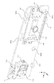
- FIG. 1 shows a schematic configuration of the object detection apparatus according to the present embodiment.
- the object detection device includes an information acquisition device 1 and an information processing device 2.
- the television 3 is controlled by a signal from the information processing device 2.
- a device including the information acquisition device 1 and the information processing device 2 corresponds to the object detection device of the present invention.
- the information acquisition device 1 projects infrared light over the entire target area and receives the reflected light with a CMOS image sensor, whereby the distance between each part of the object in the target area (hereinafter referred to as “three-dimensional distance information”). To get.
- the acquired three-dimensional distance information is sent to the information processing apparatus 2 via the cable 4.
- the information processing apparatus 2 is, for example, a controller for TV control, a game machine, a personal computer, or the like.
- the information processing device 2 detects an object in the target area based on the three-dimensional distance information received from the information acquisition device 1, and controls the television 3 based on the detection result.
- the information processing apparatus 2 detects a person based on the received three-dimensional distance information and detects the movement of the person from the change in the three-dimensional distance information.
- the information processing device 2 is a television control controller
- the information processing device 2 detects the person's gesture from the received three-dimensional distance information and outputs a control signal to the television 3 in accordance with the gesture.
- the application program to be installed is installed.
- the user can cause the television 3 to execute a predetermined function such as channel switching or volume up / down by making a predetermined gesture while watching the television 3.
- the information processing device 2 when the information processing device 2 is a game machine, the information processing device 2 detects the person's movement from the received three-dimensional distance information, and displays a character on the television screen according to the detected movement.
- An application program that operates and changes the game battle situation is installed. In this case, the user can experience a sense of realism in which he / she plays a game as a character on the television screen by making a predetermined movement while watching the television 3.
- FIG. 2 is a diagram showing the configuration of the information acquisition device 1 and the information processing device 2.
- the information acquisition apparatus 1 includes a projection optical system 11 and a light receiving optical system 12 as a configuration of the optical unit.
- the information acquisition device 1 includes a CPU (Central Processing Unit) 21, a laser driving circuit 22, an imaging signal processing circuit 23, an input / output circuit 24, and a memory 25 as a circuit unit.
- CPU Central Processing Unit
- the projection optical system 11 irradiates a target area with laser light having a predetermined dot pattern.
- the light receiving optical system 12 receives the laser beam reflected from the target area.
- the configurations of the projection optical system 11 and the light receiving optical system 12 will be described later with reference to FIGS.
- the CPU 21 controls each unit according to a control program stored in the memory 25.
- the CPU 21 has functions of a laser control unit 21 a for controlling a laser light source 111 (described later) in the projection optical system 11 and a three-dimensional distance calculation unit 21 b for generating three-dimensional distance information. Is granted.
- the laser drive circuit 22 drives a laser light source 111 (described later) according to a control signal from the CPU 21.
- the imaging signal processing circuit 23 controls a CMOS image sensor 123 (described later) in the light receiving optical system 12 and sequentially takes in each pixel signal (charge) generated by the CMOS image sensor 123 for each line. Then, the captured signals are sequentially output to the CPU 21.
- CPU21 calculates the distance from the information acquisition apparatus 1 to each part of a detection target based on the signal (imaging signal) supplied from the imaging signal processing circuit 23 by the process by the three-dimensional distance calculation part 21b.
- the input / output circuit 24 controls data communication with the information processing apparatus 2.
- the information processing apparatus 2 includes a CPU 31, an input / output circuit 32, and a memory 33.
- the information processing apparatus 2 has a configuration for performing communication with the television 3 and for reading information stored in an external memory such as a CD-ROM and installing it in the memory 33.
- an external memory such as a CD-ROM
- the configuration of these peripheral circuits is not shown for the sake of convenience.
- the CPU 31 controls each unit according to a control program (application program) stored in the memory 33.
- a control program application program
- the CPU 31 is provided with the function of the object detection unit 31a for detecting an object in the image.
- a control program is read from a CD-ROM by a drive device (not shown) and installed in the memory 33, for example.
- the object detection unit 31a detects a person in the image and its movement from the three-dimensional distance information supplied from the information acquisition device 1. Then, a process for operating the character on the television screen according to the detected movement is executed by the control program.
- the object detection unit 31 a detects a person in the image and its movement (gesture) from the three-dimensional distance information supplied from the information acquisition device 1. To do. Then, processing for controlling functions (channel switching, volume adjustment, etc.) of the television 3 is executed by the control program in accordance with the detected movement (gesture).
- the input / output circuit 32 controls data communication with the information acquisition device 1.
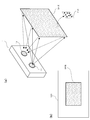
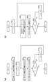
- FIG. 3 is a perspective view showing an installation state of the projection optical system 11 and the light receiving optical system 12.
- the projection optical system 11 and the light receiving optical system 12 are installed on a base plate 300 having high thermal conductivity.
- the optical members constituting the projection optical system 11 are installed on the chassis 11 a, and the chassis 11 a is installed on the base plate 300. Thereby, the projection optical system 11 is installed on the base plate 300.
- the light receiving optical system 12 is installed on the upper surface of the two pedestals 300a on the base plate 300 and the upper surface of the base plate 300 between the two pedestals 300a.
- a CMOS image sensor 123 described later is installed on the upper surface of the base plate 300 between the two pedestals 300a, and a holding plate 12a is installed on the upper surface of the pedestal 300a.
- a lens holder 12b for holding 122 is installed.
- the projection optical system 11 and the light receiving optical system 12 are installed side by side with a predetermined distance in the X axis direction so that the projection center of the projection optical system 11 and the imaging center of the light receiving optical system 12 are aligned on a straight line parallel to the X axis.
- a circuit board 200 (see FIG. 4) that holds the circuit unit (see FIG. 2) of the information acquisition device 1 is installed on the back surface of the base plate 300.
- a hole 300 b for taking out the wiring of the laser light source 111 to the back of the base plate 300 is formed in the lower center of the base plate 300.
- an opening 300 c for exposing the connector 12 c of the CMOS image sensor 123 to the back of the base plate 300 is formed below the installation position of the light receiving optical system 12 on the base plate 300.
- FIG. 4 is a diagram schematically showing the configuration of the projection optical system 11 and the light receiving optical system 12 according to the present embodiment.
- the projection optical system 11 includes a laser light source 111, a collimator lens 112, a rising mirror 113, and a diffractive optical element (DOE: Diffractive Optical Element) 114.
- the light receiving optical system 12 includes a filter 121, an imaging lens 122, and a CMOS image sensor 123.
- the laser light source 111 outputs laser light in a narrow wavelength band with a wavelength of about 830 nm.
- the laser light source 111 is installed so that the optical axis of the laser light is parallel to the X axis.
- the collimator lens 112 converts the laser light emitted from the laser light source 111 into substantially parallel light.
- the collimator lens 112 is installed so that its own optical axis is aligned with the optical axis of the laser light emitted from the laser light source 111.
- the raising mirror 113 reflects the laser beam incident from the collimator lens 112 side.
- the optical axis of the laser beam is bent 90 ° by the rising mirror 113 and becomes parallel to the Z axis.
- the DOE 114 has a diffraction pattern on the incident surface.
- the diffraction pattern is composed of, for example, a step type hologram. Due to the diffractive action of this diffraction pattern, the laser light reflected by the rising mirror 113 and incident on the DOE 114 is converted into a laser light having a dot pattern and irradiated onto the target area.
- the diffraction pattern is designed to be a predetermined dot pattern in the target area.
- an aperture (not shown) for making the contour of the laser light circular is arranged between the laser light source 111 and the collimator lens 112. Note that this aperture may be constituted by an emission opening of the laser light source 111.
- the laser light reflected from the target area passes through the filter 121 and enters the imaging lens 122.
- the filter 121 transmits light in a wavelength band including the emission wavelength (about 830 nm) of the laser light source 111 and cuts other wavelength bands.
- the imaging lens 122 condenses the light incident through the filter 121 on the CMOS image sensor 123.
- the imaging lens 122 includes a plurality of lenses, and an aperture and a spacer are interposed between the predetermined lenses. Such an aperture stops the light from the outside so as to match the F number of the imaging lens 122.
- the CMOS image sensor 123 receives the light collected by the imaging lens 122 and outputs a signal (charge) corresponding to the amount of received light to the imaging signal processing circuit 23 for each pixel.
- the output speed of the signal is increased so that the signal (charge) of the pixel can be output to the imaging signal processing circuit 23 with high response from the light reception in each pixel.
- the filter 121 is arranged so that the light receiving surface is perpendicular to the Z axis.
- the imaging lens 122 is installed so that the optical axis is parallel to the Z axis.
- the CMOS image sensor 123 is installed such that the light receiving surface is perpendicular to the Z axis.
- the filter 121, the imaging lens 122, and the CMOS image sensor 123 are arranged so that the center of the filter 121 and the center of the light receiving region of the CMOS image sensor 123 are aligned on the optical axis of the imaging lens 122.
- the projection optical system 11 and the light receiving optical system 12 are installed on the base plate 300 as described with reference to FIG.
- a circuit board 200 is further installed on the lower surface of the base plate 300, and wirings (flexible boards) 201 and 202 are connected from the circuit board 200 to the laser light source 111 and the CMOS image sensor 123.
- the circuit unit of the information acquisition apparatus 1 such as the CPU 21 and the laser driving circuit 22 shown in FIG.
- FIG. 5A is a diagram schematically showing the irradiation state of the laser light on the target region
- FIG. 5B is a diagram schematically showing the light receiving state of the laser light in the CMOS image sensor 123.
- FIG. 6B shows a light receiving state when a flat surface (screen) exists in the target area.
- the projection optical system 11 emits laser light having a dot pattern (hereinafter, the entire laser light having this pattern is referred to as “DP light”) toward the target region. Is done.
- the DP light projection area is indicated by a solid frame.
- dot regions hereinafter simply referred to as “dots” in which the intensity of the laser light is increased by the diffractive action of the diffractive optical element are scattered according to the dot pattern by the diffractive action of the diffractive optical element.
- dots dot regions in which the intensity of the laser light is increased by the diffractive action of the diffractive optical element are scattered according to the dot pattern by the diffractive action of the diffractive optical element.
- a flat reflection plane RS perpendicular to the Z-axis direction is disposed at a predetermined distance Ls from the projection optical system 11.
- the temperature of the laser light source 111 is maintained at a predetermined temperature (reference temperature).
- DP light is emitted from the projection optical system 11 for a predetermined time Te.
- the emitted DP light is reflected by the reflection plane RS and enters the CMOS image sensor 123 of the light receiving optical system 12.
- an electrical signal for each pixel is output from the CMOS image sensor 123.
- the output electric signal value (pixel value) for each pixel is developed on the memory 25 of FIG.
- a reference pattern region that defines the DP light irradiation region on the CMOS image sensor 123 is set as shown in FIG. 6B.
- segment area (comparative example) set as a reference pattern area will be described with reference to FIGS.
- each segment area has the same size as all the other segment areas, and two segment areas adjacent in the vertical and horizontal directions are set so as to overlap each other with a shift of one pixel as shown in FIG.
- each segment area is dotted with dots in a unique pattern, the pattern of pixel values in the segment area differs for each segment area.
- the pixel value of each pixel included in the segment area is assigned to each segment area.
- information on the position of the reference pattern area on the CMOS image sensor 123 information on the pixel values (reference patterns) of all pixels included in the reference pattern area, the size (width and width) of the segment area, and each segment area Information regarding the position on the reference pattern area is a reference template.
- the pixel values (reference patterns) of all the pixels included in the reference pattern region correspond to the DP light dot pattern included in the reference pattern region.
- a segment area defined by information on the size of the segment area and information on the position of each segment area on the reference pattern area is mapped to the mapping area of the pixel values (reference patterns) of all the pixels included in the reference pattern area. By setting, the pixel value of the pixel included in each segment area is acquired.
- the reference template in this case may further hold the pixel values of the pixels included in each segment area for each segment area in advance.
- the configured reference template is held in the memory 25 of FIG. 2 in an unerasable state.
- the reference template thus stored in the memory 25 is referred to by the CPU 21 when calculating the distance from the projection optical system 11 to each part of the detection target object.
- DP light corresponding to a predetermined segment area Sn on the reference pattern is reflected by the object, and the segment area The light enters a region Sn ′ different from Sn. Since the projection optical system 11 and the light receiving optical system 12 are adjacent to each other in the X-axis direction, the displacement direction of the region Sn ′ with respect to the segment region Sn is parallel to the X-axis. In the case of FIG. 6A, since the object is at a position closer than the distance Ls, the region Sn ′ is displaced in the positive direction of the X axis with respect to the segment region Sn. If the object is at a position farther than the distance Ls, the region Sn ′ is displaced in the negative X-axis direction with respect to the segment region Sn.
- the distance Lr from the projection optical system 11 to the portion of the object irradiated with DP light (DPn) is triangulated using the distance Ls. Calculated based on Similarly, the distance from the projection optical system 11 is calculated for the part of the object corresponding to another segment area.
- Non-Patent Document 1 The 19th Annual Conference of the Robotics Society of Japan (September 18-20, 2001) Proceedings, P1279-1280).
- FIG. 7 is a diagram for explaining such a detection method using the segment regions (comparative examples) shown in FIGS. 6B and 6C.
- FIG. 5A is a diagram showing the setting state of the reference pattern region and the segment region on the CMOS image sensor 123
- FIG. 5B is a diagram showing a method for searching the segment region at the time of actual measurement
- FIG. These are figures which show the collation method with the dot pattern of measured DP light, and the dot pattern contained in the segment area
- the segment area S1 is one pixel in the X-axis direction in the range P1 to P2.
- the matching degree between the dot pattern of the segment area S1 and the actually measured dot pattern of DP light is obtained.
- the segment area S1 is sent in the X-axis direction only on the line L1 passing through the uppermost segment area group of the reference pattern area. This is because, as described above, each segment region is normally displaced only in the X-axis direction from the position set by the reference template at the time of actual measurement. That is, the segment area S1 is considered to be on the uppermost line L1.
- the processing load for the search is reduced.
- the segment area may protrude from the reference pattern area in the X-axis direction. Therefore, the ranges P1 and P2 are set wider than the width of the reference pattern area in the X-axis direction.
- a region (comparison region) having the same size as the segment region S1 is set on the line L1, and the similarity between the comparison region and the segment region S1 is obtained. That is, the difference between the pixel value of each pixel in the segment area S1 and the pixel value of the corresponding pixel in the comparison area is obtained. A value Rsad obtained by adding the obtained difference to all the pixels in the comparison region is acquired as a value indicating the similarity.
- the pixel values T (i, j) of the i columns and j rows of pixels in the segment area are included in one segment area.
- the pixel value I (i, j) of the pixel in the comparison area i column and j row is obtained from the sum of the differences. That is, the value Rsad is calculated by the following equation.
- the comparison area is sequentially set while being shifted by one pixel on the line L1. Then, the value Rsad is obtained for all the comparison regions on the line L1. A value smaller than the threshold value is extracted from the obtained value Rsad. If there is no value Rsad smaller than the threshold value, the search for the segment area S1 is regarded as an error. Then, it is determined that the comparison area corresponding to the extracted Rsad having the smallest value is the movement area of the segment area S1. The same search as described above is performed for the segment areas other than the segment area S1 on the line L1. Similarly, the segment areas on the other lines are searched by setting the comparison area on the lines as described above.
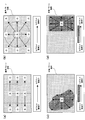
- the inventor of the present application sets all the segment areas to the same size as described above, the size of the segment areas to be set is changed and the accuracy of distance detection is verified.
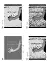
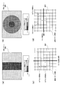
- FIG. 8A is a diagram showing the mannequin hand positioned in the target area used in this verification.
- the base and bar regions are indicated by white broken lines.
- FIGS. 8B to 8D show distance measurement results when the size of the segment region is changed to 15 ⁇ 15 pixels, 11 ⁇ 11 pixels, and 7 ⁇ 7 pixels, respectively.
- the position of the segment area where the measured distance is closer to white as the measured distance is longer and the distance measurement is in error that is, the position where the search for the segment area is in error is black. It has become.
- the ratios (error rates) of the area where the distance could not be detected properly are 8%, 12%, and 24%, respectively. That is, when the size of the segment area is set to 15 ⁇ 15 pixels or 11 ⁇ 11 pixels, the error rate is suppressed low, and the shape of the mannequin finger is also detected approximately appropriately. On the other hand, when the size of the segment area is set to 7 ⁇ 7 pixels, the error rate increases, and it becomes difficult to properly detect the shape of the mannequin finger.
- the accuracy of distance detection of the target object in the target area changes. For example, when the area of the segment region is doubled, the number of dots included in the segment region is also approximately doubled. Thereby, the uniqueness of the dot pattern included in the segment area is enhanced, and the displacement position of the segment area is easily searched for appropriately. Therefore, when it is desired to increase the accuracy of distance detection, it is desirable to set the segment area size large.
- the amount of calculation of the value Rsad increases when searching for the displacement position of each segment area, and the processing amount of the CPU 21 increases. For example, when the area of the segment region is doubled, the amount of calculation of the value Rsad is doubled.
- the size of the segment area at a predetermined position is set to be large so as to reduce the calculation amount while increasing the accuracy of distance detection.
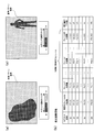
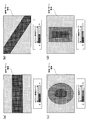
- FIG. 9A is a schematic diagram showing the size of the segment area set with respect to the reference pattern area in the present embodiment.
- the size of the segment area is set to be large in the area extending in the vertical direction at the center of the reference pattern area, and the size of the segment area is set to be small in other areas of the reference pattern area. . In this way, the accuracy of distance detection is increased in the vertical direction at the center of the target area, and the processing amount is reduced for other areas.
- the scene where the object detection device is used is standing in the center of the target area when, for example, a person standing in the center of the target area is often detected. It becomes possible to detect a person appropriately. Further, although the detection accuracy is slightly lowered at the left and right ends of the target area, the size of the segment area is set to be small, so that the processing amount of the CPU 21 can be reduced.
- the area where the segment area size is increased is set according to the area where the accuracy of distance detection is to be increased, or the area where the segment area size is decreased is determined according to the area where distance detection accuracy is not required. If set, the effects of the present invention can be remarkably exhibited. Note that the size of the segment area may be set so that these effects can be exhibited. For example, in FIG. 9A, the size of the segment area in the center extending in the vertical direction is set to 15 ⁇ 15 pixels, and the size of the segment areas in the other areas is set to 7 ⁇ 7 pixels.
- the size of the segment region is increased in the circular region at the center of the reference pattern. Is set.
- the size of the segment area may be changed stepwise in accordance with the distance from the center of the reference pattern area.
- the position of each segment area on the reference pattern area is defined by the position of the center of each segment area.
- the center of each segment area coincides with the position of any one pixel included in the reference pattern area.
- the segment regions adjacent to each other vertically and horizontally have their center positions shifted from each other by one pixel vertically and horizontally.
- the boundary extends in the vertical direction.
- a segment region Sa having a size of 3 ⁇ 3 pixels and a segment region Sb having a size of 5 ⁇ 5 pixels are adjacent to each other, if the center of the segment region exceeds the boundary in the left-right direction, The size of the region changes from 3 ⁇ 3 pixels to 5 ⁇ 5 pixels.
- the size of the segment area changes when the center of the segment area exceeds the boundary in the vertical direction.
- the size of the segment area Sm is 3 ⁇ 3 pixels
- the size of the segment area Sn is 5 ⁇ 5 pixels.
- the boundaries between regions having different segment region sizes are not circular arcs, but are step-like shapes that connect vertical and horizontal line segments at the pixel level. Also in this case, as in the case of FIGS. 9C and 9D, when the center of the segment area exceeds the boundary in the vertical direction or the horizontal direction, the size of the segment area changes.
- information defining the position of the segment area (position of the center of the segment area) and the size is set for each segment area and held in the reference template.
- the information defining the size is defined so that the size of the segment region changes in the segment regions adjacent to each other with the boundary as described above.
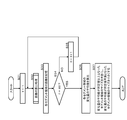
- FIG. 10A is a flowchart showing a dot pattern setting process for the segment area. Such processing is performed when the information acquisition apparatus 1 is activated or when distance detection is started. It is assumed that N segment areas are allocated to the reference pattern area, and these segment areas are assigned serial numbers from 1 to N. As described above, the position (size of the center of the segment area) and the size on the reference pattern area are defined for each segment area.
- the CPU 21 of the information acquisition apparatus 1 reads out information on the position of the reference pattern area on the CMOS image sensor 123 and the pixel values of all the pixels included in the reference pattern area from the reference template held in the memory 25 ( S11). Subsequently, the CPU 21 sets 1 to the variable k (S12).
- the CPU 21 acquires information on the size (vertical and horizontal width) of the kth segment area Sk and information on the position of the segment area Sk from the reference template stored in the memory 25 (S13). Subsequently, the CPU 21 sets the dot pattern Dk used for the search from the pixel values of all the pixels included in the reference pattern area and the information on the segment area Sk acquired in S13 (S14). Specifically, the CPU 21 sets the segment area Sk in the reference pattern area, acquires the pixel value of the dot pattern included in the segment area Sk among the pixel values of all the pixels of the reference pattern, and uses this to search A dot pattern Dk is assumed.
- the CPU 21 determines whether the value of k is equal to N (S15).
- the dot pattern used for the search is set for all the segment areas and the value of k becomes N (S15: YES)
- the process ends.
- the CPU 21 increases the value of k by 1 (S16), and returns the process to S13. In this way, N dot patterns used for the search are sequentially set.
- FIG. 10B is a flowchart showing the distance detection process at the time of actual measurement. Such processing is performed using the search dot pattern set by the processing of FIG. 10A, and is performed in parallel with the processing of FIG.
- the CPU 21 of the information acquisition device 1 first sets 1 to the variable c (S21). Next, the CPU 21 searches the dot pattern on the CMOS image sensor 123 received during the actual measurement for a region that matches the c-th search dot pattern Dc set in S14 of FIG. 10A (S22). Such a search is performed on an area having a predetermined width in the left-right direction with respect to a position corresponding to the segment area Sc. If there is an area that matches the search dot pattern Dc, the CPU 21 detects how far the matched area has moved in the left or right direction from the position of the segment area Sc, and the detected movement direction and movement. Using the distance, the distance of the object located in the segment area Sc is calculated based on the triangulation method (S23).
- the CPU 21 determines whether the value of c is equal to N (S24). The distance is calculated for all the segment areas, and when the value of c becomes N (S24: YES), the process ends. On the other hand, if the value of c has not reached N (S24: NO), the CPU 21 increases the value of c by 1 (S25), and returns the process to S22. Thus, the distance to the detection target object corresponding to the segment area is obtained.
- the size of the segment area is set large in the area where the accuracy of distance detection is to be improved, and the segment area is set in other areas.
- the size of is set small. As a result, the accuracy of distance detection of the target object can be improved and the processing amount of the CPU 21 can be reduced.
- the CMOS image sensor 123 is used as the photodetector, but a CCD image sensor may be used instead.
- the laser light source 111 and the collimator lens 112 are arranged in the X-axis direction, and the optical axis of the laser beam is bent in the Z-axis direction by the rising mirror 113.
- the laser light source 111 may be arranged so as to emit, and the laser light source 111, the collimator lens 112, and the DOE 114 may be arranged side by side in the Z-axis direction.
- the rising mirror 113 can be omitted, but the dimension of the projection optical system 11 increases in the Z-axis direction.
- the size of the segment area is set in advance with respect to the reference pattern area.
- the size of the segment area may be set as appropriate based on the detected distance.
- FIG. 11A is a schematic diagram showing the size of the segment area when the size of the segment area is set larger than the area where the change in the detection distance is large. As shown in the drawing, when the distance of the target object is determined to be large (the change in the detection distance is large) as a result of the distance detection near the left side of the reference pattern area, the size of the segment area in this area is set large. .
- the standard template holds two sizes, a large size and a small size, as the size (width and width) of the segment area.
- all segment areas are set to a small size.
- the size of the segment area corresponding to this portion is changed to a large size.
- the size of the segment area corresponding to this part is returned to a small size.
- FIG. 11B is a diagram schematically showing detection distance information used when determining the amount of movement of the target object.
- the detection distance information is stored in the memory 25.
- the memory 25 stores 60 distances acquired by the process of FIG. 10B for each image (frame) captured by the CMOS image sensor 123 every 1/60 seconds as detection distance information. That is, the distances Fc (1) to Fc (60) are stored per second for the segment area Sc. Further, the distance Fc (0) of the previous frame 60 is included in the detected distance information. Note that immediately after the apparatus is activated, the distance value of the previous frame 60 is set to 0, for example.
- the average value of the amount of change is acquired based on the previous distance of the frame 60 and the distance of the frames 1 to 60. That is, for the segment region Sc, first, the sum of changes is ⁇ Fc (1) ⁇ Fc (0) ⁇ + ⁇ Fc (2) ⁇ Fc (1) ⁇ + ⁇ Fc (3) ⁇ Fc (2) ⁇ + ... + ⁇ F (60) ⁇ F (59) ⁇
- an average value Vc of the change amounts is obtained.
- the segment areas that are equal to or greater than a predetermined value are determined to be areas that have a large change in the detection distance.
- FIG. 12 is a flowchart showing the segment area resetting process in this case.
- the distance is measured every 1/60 seconds.
- the CPU 21 of the information acquisition device 1 first sets 1 to the variable f (S31). Subsequently, the CPU 21 calculates the distance to the target object corresponding to each segment area according to the process shown in FIG. 10B (S32).
- CPU21 memorize
- the CPU 21 determines whether the value of f is equal to 60 (S34). If the value of f has not reached 60 (S34: NO), the CPU 21 increases the value of f by 1 (S35), and returns the process to S32. On the other hand, when the repetition distance is calculated and the value of f reaches 60 (S34: YES), the process proceeds to S36.
- the CPU 21 calculates the average values V1 to VN of the change amounts of the segment areas as described with reference to FIG. 11B (S36). Subsequently, the CPU 21 sets the size of the segment area that is greater than or equal to the predetermined value among the average values V1 to VN of the change amount to be larger and sets the size of the segment area that is smaller than the predetermined value to be smaller. (S37). Such setting is performed by applying one of two sizes (vertical and horizontal widths) of the segment area held in the reference template.
- the size of the segment area where the average value of the change amount is equal to or greater than the predetermined value is set to 15 ⁇ 15 pixels, and the size of the segment area where the average value of the change amount is less than the predetermined amount is set to 7 ⁇ 7 pixels. Is done.
- the process of resetting the segment area (S31 to S37) is repeatedly performed, so that the accuracy of distance detection with respect to the target object having a large movement amount can be improved, and the processing amount of the CPU 21 can be reduced.
- the size of the segment area is switched to two stages, but the size of the segment area may be switched to three or more stages according to the average value of the change amounts.
- other values indicating the amount of change such as a total value of the amount of change during a predetermined period may be used.
- the size of the segment area corresponding to this area is set large, and the area corresponds to another area.
- the size of the segment area may be set small.
- the segment area size is set to change stepwise.
- the present invention is not limited to this, and the segment area size may be set to change linearly.
- the size of the segment area is set to be the largest in the center in the left-right direction of the reference pattern area, You may set so that the size of a segment area
- region may become small as it goes to an edge part.
- the size of the segment area is set to be the largest at the center of the reference pattern area, and the segment area is concentrically separated from the center. You may set so that a size may become small.
- the size of the segment area may be set linearly according to the average value of the change amount.
- the segment area increases from the center toward the end in the vicinity of this area. The size may be set smaller.
- the size of the segment area is set to be larger in the area.
- the present invention is not limited to this, and when it is desired to increase the accuracy of distance detection with respect to the center of the target region in the vertical direction or the region extending in the diagonal direction, as shown in FIG. 14 (a) or (b),
- the segment area may be set to have a large size in the central portion in the vertical direction of the reference pattern area or in the diagonally extending area.
- the size of the segment area is set to be large in the circular area at the center of the reference pattern area. It was.
- the present invention is not limited to this, and when the target object positioned at the center of the target area often has a predetermined shape, an area having a large segment area may be set according to the shape of the target object. For example, if the shape of the target object is an elliptical shape that is long in the vertical direction, the size of the segment area may be set so as to decrease stepwise as it moves away from the center as shown in FIG. good.
- the shape of the target object is a rectangular shape extending in the vertical direction
- the size of the segment area is gradually reduced as the distance from the center increases to the rectangular shape extending in the vertical direction, as shown in FIG. It may be set to be.
- each segment area is set so as to overlap each other with a shift of one pixel.
- the present invention is not limited to this. It may be set as follows. Further, each segment area may be set so as to overlap only in one of the left and right directions and the up and down direction, or may be set so that adjacent segment areas do not overlap at all.
Abstract
Priority Applications (3)
| Application Number | Priority Date | Filing Date | Title |
|---|---|---|---|
| CN2012800006257A CN102859320A (zh) | 2011-04-28 | 2012-04-06 | 信息取得装置以及物体检测装置 |
| JP2012529036A JP5214062B1 (ja) | 2011-04-28 | 2012-04-06 | 情報取得装置および物体検出装置 |
| US13/616,611 US20130002860A1 (en) | 2011-04-28 | 2012-09-14 | Information acquiring device and object detecting device |
Applications Claiming Priority (2)
| Application Number | Priority Date | Filing Date | Title |
|---|---|---|---|
| JP2011-101666 | 2011-04-28 | ||
| JP2011101666 | 2011-04-28 |
Related Child Applications (1)
| Application Number | Title | Priority Date | Filing Date |
|---|---|---|---|
| US13/616,611 Continuation US20130002860A1 (en) | 2011-04-28 | 2012-09-14 | Information acquiring device and object detecting device |
Publications (1)
| Publication Number | Publication Date |
|---|---|
| WO2012147495A1 true WO2012147495A1 (fr) | 2012-11-01 |
Family
ID=47072019
Family Applications (1)
| Application Number | Title | Priority Date | Filing Date |
|---|---|---|---|
| PCT/JP2012/059449 WO2012147495A1 (fr) | 2011-04-28 | 2012-04-06 | Dispositif d'acquisition d'informations et dispositif de détection d'objet |
Country Status (4)
| Country | Link |
|---|---|
| US (1) | US20130002860A1 (fr) |
| JP (1) | JP5214062B1 (fr) |
| CN (1) | CN102859320A (fr) |
| WO (1) | WO2012147495A1 (fr) |
Cited By (3)
| Publication number | Priority date | Publication date | Assignee | Title |
|---|---|---|---|---|
| WO2016056628A1 (fr) * | 2014-10-09 | 2016-04-14 | シャープ株式会社 | Dispositif et programme de traitement de reconnaissance d'image |
| JP2016186680A (ja) * | 2015-03-27 | 2016-10-27 | セイコーエプソン株式会社 | インタラクティブプロジェクターおよびインタラクティブプロジェクターの制御方法 |
| JP6410198B1 (ja) * | 2016-08-12 | 2018-10-24 | パナソニックIpマネジメント株式会社 | 測距システム、および、移動体システム |
Families Citing this family (6)
| Publication number | Priority date | Publication date | Assignee | Title |
|---|---|---|---|---|
| US9294758B2 (en) | 2013-04-18 | 2016-03-22 | Microsoft Technology Licensing, Llc | Determining depth data for a captured image |
| KR101386248B1 (ko) * | 2013-09-09 | 2014-04-17 | 재단법인 실감교류인체감응솔루션연구단 | 공간 제스처 인식 장치 및 방법 |
| CN106251810B (zh) * | 2016-08-19 | 2019-09-27 | 深圳市华星光电技术有限公司 | Amoled显示屏驱动方法、驱动电路及显示装置 |
| CN108226939B (zh) * | 2016-12-22 | 2022-03-08 | 异奇科技股份有限公司 | 通过绕射光学元件产生激光图案的路径侦测系统及其方法 |
| US10789727B2 (en) * | 2017-05-18 | 2020-09-29 | Panasonic Intellectual Property Corporation Of America | Information processing apparatus and non-transitory recording medium storing thereon a computer program |
| US11155226B2 (en) * | 2018-08-17 | 2021-10-26 | Veoneer Us, Inc. | Vehicle cabin monitoring system |
Citations (10)
| Publication number | Priority date | Publication date | Assignee | Title |
|---|---|---|---|---|
| JPH07152895A (ja) * | 1993-11-29 | 1995-06-16 | Canon Inc | 画像処理方法及び装置 |
| JP2001184497A (ja) * | 1999-10-14 | 2001-07-06 | Komatsu Ltd | ステレオ画像処理装置及び記録媒体 |
| JP2004191092A (ja) * | 2002-12-09 | 2004-07-08 | Ricoh Co Ltd | 3次元情報取得システム |
| JP2005246033A (ja) * | 2004-02-04 | 2005-09-15 | Sumitomo Osaka Cement Co Ltd | 状態解析装置 |
| JP2007218922A (ja) * | 2007-03-27 | 2007-08-30 | Topcon Corp | 画像測定装置 |
| WO2008041518A1 (fr) * | 2006-10-02 | 2008-04-10 | Konica Minolta Holdings, Inc. | Dispositif de traitement d'images, procédé de commande pour un dispositif de traitement d'images et programme de commande pour un dispositif de traitement d'images |
| JP2009014712A (ja) * | 2007-06-07 | 2009-01-22 | Univ Of Electro-Communications | 物体検出装置とそれを適用したゲート装置 |
| JP2009092551A (ja) * | 2007-10-10 | 2009-04-30 | Konica Minolta Holdings Inc | 障害物計測方法、障害物計測装置及び障害物計測システム |
| JP2010101683A (ja) * | 2008-10-22 | 2010-05-06 | Nissan Motor Co Ltd | 距離計測装置および距離計測方法 |
| JP2011022072A (ja) * | 2009-07-17 | 2011-02-03 | Nikon Corp | 位置検出装置 |
Family Cites Families (18)
| Publication number | Priority date | Publication date | Assignee | Title |
|---|---|---|---|---|
| JPH0615968B2 (ja) * | 1986-08-11 | 1994-03-02 | 伍良 松本 | 立体形状測定装置 |
| US4967093A (en) * | 1988-06-22 | 1990-10-30 | Hamamatsu Photonics Kabushiki Kaisha | Deformation measuring method and device using cross-correlation function between speckle patterns with reference data renewal |
| US4948258A (en) * | 1988-06-27 | 1990-08-14 | Harbor Branch Oceanographic Institute, Inc. | Structured illumination surface profiling and ranging systems and methods |
| US5075562A (en) * | 1990-09-20 | 1991-12-24 | Eastman Kodak Company | Method and apparatus for absolute Moire distance measurements using a grating printed on or attached to a surface |
| JP3357210B2 (ja) * | 1995-02-03 | 2002-12-16 | 株式会社日立国際電気 | 自動焦点検出方法 |
| JPH10143659A (ja) * | 1996-11-06 | 1998-05-29 | Komatsu Ltd | 物体検出装置 |
| US6125197A (en) * | 1998-06-30 | 2000-09-26 | Intel Corporation | Method and apparatus for the processing of stereoscopic electronic images into three-dimensional computer models of real-life objects |
| FR2830079B1 (fr) * | 2001-09-26 | 2004-04-30 | Holo 3 | Procede et dispositif de mesure d'au moins une grandeur geometrique d'une surface optiquement reflechissante |
| AU2003245628A1 (en) * | 2002-06-19 | 2004-01-06 | Canesta, Inc. | System and method for determining 3-d coordinates of a surface using a coded array |
| JP4352808B2 (ja) * | 2002-09-18 | 2009-10-28 | セイコーエプソン株式会社 | プレビュー装置、電子機器および画像形成装置 |
| US7103212B2 (en) * | 2002-11-22 | 2006-09-05 | Strider Labs, Inc. | Acquisition of three-dimensional images by an active stereo technique using locally unique patterns |
| CN101288105B (zh) * | 2005-10-11 | 2016-05-25 | 苹果公司 | 用于物体重现的方法和系统 |
| US8390821B2 (en) * | 2005-10-11 | 2013-03-05 | Primesense Ltd. | Three-dimensional sensing using speckle patterns |
| JP2007187956A (ja) * | 2006-01-16 | 2007-07-26 | Matsushita Electric Ind Co Ltd | 画像出力装置、出力画像制御方法および出力画像制御プログラム |
| US8090194B2 (en) * | 2006-11-21 | 2012-01-03 | Mantis Vision Ltd. | 3D geometric modeling and motion capture using both single and dual imaging |
| US8730524B2 (en) * | 2007-08-14 | 2014-05-20 | Ricoh Company, Ltd. | Image processing apparatus to correct an image during double-sided printing |
| US8649025B2 (en) * | 2010-03-27 | 2014-02-11 | Micrometric Vision Technologies | Methods and apparatus for real-time digitization of three-dimensional scenes |
| US8724887B2 (en) * | 2011-02-03 | 2014-05-13 | Microsoft Corporation | Environmental modifications to mitigate environmental factors |
-
2012
- 2012-04-06 CN CN2012800006257A patent/CN102859320A/zh active Pending
- 2012-04-06 JP JP2012529036A patent/JP5214062B1/ja not_active Expired - Fee Related
- 2012-04-06 WO PCT/JP2012/059449 patent/WO2012147495A1/fr active Application Filing
- 2012-09-14 US US13/616,611 patent/US20130002860A1/en not_active Abandoned
Patent Citations (10)
| Publication number | Priority date | Publication date | Assignee | Title |
|---|---|---|---|---|
| JPH07152895A (ja) * | 1993-11-29 | 1995-06-16 | Canon Inc | 画像処理方法及び装置 |
| JP2001184497A (ja) * | 1999-10-14 | 2001-07-06 | Komatsu Ltd | ステレオ画像処理装置及び記録媒体 |
| JP2004191092A (ja) * | 2002-12-09 | 2004-07-08 | Ricoh Co Ltd | 3次元情報取得システム |
| JP2005246033A (ja) * | 2004-02-04 | 2005-09-15 | Sumitomo Osaka Cement Co Ltd | 状態解析装置 |
| WO2008041518A1 (fr) * | 2006-10-02 | 2008-04-10 | Konica Minolta Holdings, Inc. | Dispositif de traitement d'images, procédé de commande pour un dispositif de traitement d'images et programme de commande pour un dispositif de traitement d'images |
| JP2007218922A (ja) * | 2007-03-27 | 2007-08-30 | Topcon Corp | 画像測定装置 |
| JP2009014712A (ja) * | 2007-06-07 | 2009-01-22 | Univ Of Electro-Communications | 物体検出装置とそれを適用したゲート装置 |
| JP2009092551A (ja) * | 2007-10-10 | 2009-04-30 | Konica Minolta Holdings Inc | 障害物計測方法、障害物計測装置及び障害物計測システム |
| JP2010101683A (ja) * | 2008-10-22 | 2010-05-06 | Nissan Motor Co Ltd | 距離計測装置および距離計測方法 |
| JP2011022072A (ja) * | 2009-07-17 | 2011-02-03 | Nikon Corp | 位置検出装置 |
Cited By (4)
| Publication number | Priority date | Publication date | Assignee | Title |
|---|---|---|---|---|
| WO2016056628A1 (fr) * | 2014-10-09 | 2016-04-14 | シャープ株式会社 | Dispositif et programme de traitement de reconnaissance d'image |
| JP2016186680A (ja) * | 2015-03-27 | 2016-10-27 | セイコーエプソン株式会社 | インタラクティブプロジェクターおよびインタラクティブプロジェクターの制御方法 |
| JP6410198B1 (ja) * | 2016-08-12 | 2018-10-24 | パナソニックIpマネジメント株式会社 | 測距システム、および、移動体システム |
| JP2019032296A (ja) * | 2016-08-12 | 2019-02-28 | パナソニックIpマネジメント株式会社 | 測距システム、および、移動体システム |
Also Published As
| Publication number | Publication date |
|---|---|
| JP5214062B1 (ja) | 2013-06-19 |
| US20130002860A1 (en) | 2013-01-03 |
| JPWO2012147495A1 (ja) | 2014-07-28 |
| CN102859320A (zh) | 2013-01-02 |
Similar Documents
| Publication | Publication Date | Title |
|---|---|---|
| JP5214062B1 (ja) | 情報取得装置および物体検出装置 | |
| JP5138116B2 (ja) | 情報取得装置および物体検出装置 | |
| WO2012137674A1 (fr) | Dispositif d'acquisition d'informations, dispositif de projection et dispositif de détection d'objets | |
| US20130050710A1 (en) | Object detecting device and information acquiring device | |
| JP5143312B2 (ja) | 情報取得装置、投射装置および物体検出装置 | |
| WO2013046927A1 (fr) | Dispositif d'acquisition d'informations et dispositif détecteur d'objet | |
| JP2012237604A (ja) | 情報取得装置、投射装置および物体検出装置 | |
| WO2012144340A1 (fr) | Dispositif d'acquisition d'informations, et dispositif de détection d'objet | |
| JP2014044113A (ja) | 情報取得装置および物体検出装置 | |
| US20120326007A1 (en) | Object detecting device and information acquiring device | |
| WO2012026180A1 (fr) | Dispositif d'acquisition d'informations et dispositif de détection d'objet | |
| JPWO2013015145A1 (ja) | 情報取得装置および物体検出装置 | |
| WO2013015146A1 (fr) | Dispositif de détection d'objet et dispositif d'acquisition d'informations | |
| WO2012120729A1 (fr) | Appareil d'acquisition d'informations et appareil de détection d'objets dans lequel est monté l'appareil d'acquisition d'informations | |
| JP2013246009A (ja) | 物体検出装置 | |
| WO2013031447A1 (fr) | Dispositif de détection d'objets et dispositif d'acquisition d'informations | |
| WO2013046928A1 (fr) | Dispositif d'acquisition d'informations et dispositif de détection d'objet | |
| JP2014085257A (ja) | 情報取得装置および物体検出装置 | |
| JP2013234956A (ja) | 情報取得装置および物体検出装置 | |
| JP2014035304A (ja) | 情報取得装置および物体検出装置 | |
| WO2013031448A1 (fr) | Dispositif de détection d'objets et dispositif d'acquisition d'informations | |
| JP5138120B2 (ja) | 物体検出装置および情報取得装置 | |
| JP2013234957A (ja) | 情報取得装置および物体検出装置 | |
| JP2014085282A (ja) | 情報取得装置および物体検出装置 | |
| JP2013234887A (ja) | 情報取得装置および物体検出装置 |
Legal Events
| Date | Code | Title | Description |
|---|---|---|---|
| WWE | Wipo information: entry into national phase |
Ref document number: 201280000625.7 Country of ref document: CN |
|
| ENP | Entry into the national phase |
Ref document number: 2012529036 Country of ref document: JP Kind code of ref document: A |
|
| 121 | Ep: the epo has been informed by wipo that ep was designated in this application |
Ref document number: 12776728 Country of ref document: EP Kind code of ref document: A1 |
|
| NENP | Non-entry into the national phase |
Ref country code: DE |
|
| 122 | Ep: pct application non-entry in european phase |
Ref document number: 12776728 Country of ref document: EP Kind code of ref document: A1 |