WO2012147280A1 - Pfc信号生成回路、それを用いたpfc制御システム、及びpfc制御方法 - Google Patents
Pfc信号生成回路、それを用いたpfc制御システム、及びpfc制御方法 Download PDFInfo
- Publication number
- WO2012147280A1 WO2012147280A1 PCT/JP2012/002341 JP2012002341W WO2012147280A1 WO 2012147280 A1 WO2012147280 A1 WO 2012147280A1 JP 2012002341 W JP2012002341 W JP 2012002341W WO 2012147280 A1 WO2012147280 A1 WO 2012147280A1
- Authority
- WO
- WIPO (PCT)
- Prior art keywords
- pfc
- signal
- circuit
- timing
- inductor
- Prior art date
- Legal status (The legal status is an assumption and is not a legal conclusion. Google has not performed a legal analysis and makes no representation as to the accuracy of the status listed.)
- Ceased
Links
Images











Classifications
-
- H—ELECTRICITY
- H02—GENERATION; CONVERSION OR DISTRIBUTION OF ELECTRIC POWER
- H02M—APPARATUS FOR CONVERSION BETWEEN AC AND AC, BETWEEN AC AND DC, OR BETWEEN DC AND DC, AND FOR USE WITH MAINS OR SIMILAR POWER SUPPLY SYSTEMS; CONVERSION OF DC OR AC INPUT POWER INTO SURGE OUTPUT POWER; CONTROL OR REGULATION THEREOF
- H02M1/00—Details of apparatus for conversion
- H02M1/42—Circuits or arrangements for compensating for or adjusting power factor in converters or inverters
- H02M1/4208—Arrangements for improving power factor of AC input
- H02M1/4225—Arrangements for improving power factor of AC input using a non-isolated boost converter
-
- H—ELECTRICITY
- H02—GENERATION; CONVERSION OR DISTRIBUTION OF ELECTRIC POWER
- H02M—APPARATUS FOR CONVERSION BETWEEN AC AND AC, BETWEEN AC AND DC, OR BETWEEN DC AND DC, AND FOR USE WITH MAINS OR SIMILAR POWER SUPPLY SYSTEMS; CONVERSION OF DC OR AC INPUT POWER INTO SURGE OUTPUT POWER; CONTROL OR REGULATION THEREOF
- H02M1/00—Details of apparatus for conversion
- H02M1/42—Circuits or arrangements for compensating for or adjusting power factor in converters or inverters
-
- H—ELECTRICITY
- H02—GENERATION; CONVERSION OR DISTRIBUTION OF ELECTRIC POWER
- H02M—APPARATUS FOR CONVERSION BETWEEN AC AND AC, BETWEEN AC AND DC, OR BETWEEN DC AND DC, AND FOR USE WITH MAINS OR SIMILAR POWER SUPPLY SYSTEMS; CONVERSION OF DC OR AC INPUT POWER INTO SURGE OUTPUT POWER; CONTROL OR REGULATION THEREOF
- H02M3/00—Conversion of DC power input into DC power output
- H02M3/02—Conversion of DC power input into DC power output without intermediate conversion into AC
- H02M3/04—Conversion of DC power input into DC power output without intermediate conversion into AC by static converters
- H02M3/10—Conversion of DC power input into DC power output without intermediate conversion into AC by static converters using discharge tubes with control electrode or semiconductor devices with control electrode
- H02M3/145—Conversion of DC power input into DC power output without intermediate conversion into AC by static converters using discharge tubes with control electrode or semiconductor devices with control electrode using devices of a triode or transistor type requiring continuous application of a control signal
- H02M3/155—Conversion of DC power input into DC power output without intermediate conversion into AC by static converters using discharge tubes with control electrode or semiconductor devices with control electrode using devices of a triode or transistor type requiring continuous application of a control signal using semiconductor devices only
- H02M3/156—Conversion of DC power input into DC power output without intermediate conversion into AC by static converters using discharge tubes with control electrode or semiconductor devices with control electrode using devices of a triode or transistor type requiring continuous application of a control signal using semiconductor devices only with automatic control of output voltage or current, e.g. switching regulators
- H02M3/158—Conversion of DC power input into DC power output without intermediate conversion into AC by static converters using discharge tubes with control electrode or semiconductor devices with control electrode using devices of a triode or transistor type requiring continuous application of a control signal using semiconductor devices only with automatic control of output voltage or current, e.g. switching regulators including plural semiconductor devices as final control devices for a single load
- H02M3/1584—Conversion of DC power input into DC power output without intermediate conversion into AC by static converters using discharge tubes with control electrode or semiconductor devices with control electrode using devices of a triode or transistor type requiring continuous application of a control signal using semiconductor devices only with automatic control of output voltage or current, e.g. switching regulators including plural semiconductor devices as final control devices for a single load with a plurality of power processing stages connected in parallel
-
- H—ELECTRICITY
- H05—ELECTRIC TECHNIQUES NOT OTHERWISE PROVIDED FOR
- H05B—ELECTRIC HEATING; ELECTRIC LIGHT SOURCES NOT OTHERWISE PROVIDED FOR; CIRCUIT ARRANGEMENTS FOR ELECTRIC LIGHT SOURCES, IN GENERAL
- H05B45/00—Circuit arrangements for operating light-emitting diodes [LED]
- H05B45/30—Driver circuits
- H05B45/37—Converter circuits
- H05B45/3725—Switched mode power supply [SMPS]
- H05B45/375—Switched mode power supply [SMPS] using buck topology
-
- H—ELECTRICITY
- H05—ELECTRIC TECHNIQUES NOT OTHERWISE PROVIDED FOR
- H05B—ELECTRIC HEATING; ELECTRIC LIGHT SOURCES NOT OTHERWISE PROVIDED FOR; CIRCUIT ARRANGEMENTS FOR ELECTRIC LIGHT SOURCES, IN GENERAL
- H05B45/00—Circuit arrangements for operating light-emitting diodes [LED]
- H05B45/30—Driver circuits
- H05B45/37—Converter circuits
- H05B45/3725—Switched mode power supply [SMPS]
- H05B45/38—Switched mode power supply [SMPS] using boost topology
-
- H—ELECTRICITY
- H05—ELECTRIC TECHNIQUES NOT OTHERWISE PROVIDED FOR
- H05B—ELECTRIC HEATING; ELECTRIC LIGHT SOURCES NOT OTHERWISE PROVIDED FOR; CIRCUIT ARRANGEMENTS FOR ELECTRIC LIGHT SOURCES, IN GENERAL
- H05B45/00—Circuit arrangements for operating light-emitting diodes [LED]
- H05B45/30—Driver circuits
- H05B45/37—Converter circuits
- H05B45/3725—Switched mode power supply [SMPS]
- H05B45/385—Switched mode power supply [SMPS] using flyback topology
-
- H—ELECTRICITY
- H02—GENERATION; CONVERSION OR DISTRIBUTION OF ELECTRIC POWER
- H02M—APPARATUS FOR CONVERSION BETWEEN AC AND AC, BETWEEN AC AND DC, OR BETWEEN DC AND DC, AND FOR USE WITH MAINS OR SIMILAR POWER SUPPLY SYSTEMS; CONVERSION OF DC OR AC INPUT POWER INTO SURGE OUTPUT POWER; CONTROL OR REGULATION THEREOF
- H02M1/00—Details of apparatus for conversion
- H02M1/0003—Details of control, feedback or regulation circuits
- H02M1/0009—Devices or circuits for detecting current in a converter
-
- H—ELECTRICITY
- H02—GENERATION; CONVERSION OR DISTRIBUTION OF ELECTRIC POWER
- H02M—APPARATUS FOR CONVERSION BETWEEN AC AND AC, BETWEEN AC AND DC, OR BETWEEN DC AND DC, AND FOR USE WITH MAINS OR SIMILAR POWER SUPPLY SYSTEMS; CONVERSION OF DC OR AC INPUT POWER INTO SURGE OUTPUT POWER; CONTROL OR REGULATION THEREOF
- H02M1/00—Details of apparatus for conversion
- H02M1/0067—Converter structures employing plural converter units, other than for parallel operation of the units on a single load
- H02M1/007—Plural converter units in cascade
-
- H—ELECTRICITY
- H02—GENERATION; CONVERSION OR DISTRIBUTION OF ELECTRIC POWER
- H02M—APPARATUS FOR CONVERSION BETWEEN AC AND AC, BETWEEN AC AND DC, OR BETWEEN DC AND DC, AND FOR USE WITH MAINS OR SIMILAR POWER SUPPLY SYSTEMS; CONVERSION OF DC OR AC INPUT POWER INTO SURGE OUTPUT POWER; CONTROL OR REGULATION THEREOF
- H02M3/00—Conversion of DC power input into DC power output
- H02M3/02—Conversion of DC power input into DC power output without intermediate conversion into AC
- H02M3/04—Conversion of DC power input into DC power output without intermediate conversion into AC by static converters
- H02M3/10—Conversion of DC power input into DC power output without intermediate conversion into AC by static converters using discharge tubes with control electrode or semiconductor devices with control electrode
- H02M3/145—Conversion of DC power input into DC power output without intermediate conversion into AC by static converters using discharge tubes with control electrode or semiconductor devices with control electrode using devices of a triode or transistor type requiring continuous application of a control signal
- H02M3/155—Conversion of DC power input into DC power output without intermediate conversion into AC by static converters using discharge tubes with control electrode or semiconductor devices with control electrode using devices of a triode or transistor type requiring continuous application of a control signal using semiconductor devices only
- H02M3/156—Conversion of DC power input into DC power output without intermediate conversion into AC by static converters using discharge tubes with control electrode or semiconductor devices with control electrode using devices of a triode or transistor type requiring continuous application of a control signal using semiconductor devices only with automatic control of output voltage or current, e.g. switching regulators
- H02M3/158—Conversion of DC power input into DC power output without intermediate conversion into AC by static converters using discharge tubes with control electrode or semiconductor devices with control electrode using devices of a triode or transistor type requiring continuous application of a control signal using semiconductor devices only with automatic control of output voltage or current, e.g. switching regulators including plural semiconductor devices as final control devices for a single load
- H02M3/1584—Conversion of DC power input into DC power output without intermediate conversion into AC by static converters using discharge tubes with control electrode or semiconductor devices with control electrode using devices of a triode or transistor type requiring continuous application of a control signal using semiconductor devices only with automatic control of output voltage or current, e.g. switching regulators including plural semiconductor devices as final control devices for a single load with a plurality of power processing stages connected in parallel
- H02M3/1586—Conversion of DC power input into DC power output without intermediate conversion into AC by static converters using discharge tubes with control electrode or semiconductor devices with control electrode using devices of a triode or transistor type requiring continuous application of a control signal using semiconductor devices only with automatic control of output voltage or current, e.g. switching regulators including plural semiconductor devices as final control devices for a single load with a plurality of power processing stages connected in parallel switched with a phase shift, i.e. interleaved
-
- Y—GENERAL TAGGING OF NEW TECHNOLOGICAL DEVELOPMENTS; GENERAL TAGGING OF CROSS-SECTIONAL TECHNOLOGIES SPANNING OVER SEVERAL SECTIONS OF THE IPC; TECHNICAL SUBJECTS COVERED BY FORMER USPC CROSS-REFERENCE ART COLLECTIONS [XRACs] AND DIGESTS
- Y02—TECHNOLOGIES OR APPLICATIONS FOR MITIGATION OR ADAPTATION AGAINST CLIMATE CHANGE
- Y02B—CLIMATE CHANGE MITIGATION TECHNOLOGIES RELATED TO BUILDINGS, e.g. HOUSING, HOUSE APPLIANCES OR RELATED END-USER APPLICATIONS
- Y02B70/00—Technologies for an efficient end-user side electric power management and consumption
- Y02B70/10—Technologies improving the efficiency by using switched-mode power supplies [SMPS], i.e. efficient power electronics conversion e.g. power factor correction or reduction of losses in power supplies or efficient standby modes
Definitions
- the present invention relates to a PFC signal generation circuit, a PFC control system using the same, and a PFC control method.
- a so-called switching power supply using a switching circuit that is periodically turned on and off is frequently used due to demands for downsizing electronic devices and reducing power consumption.
- a switching power supply for example, by using PWM (Pulse Width ⁇ Modulation) control that adjusts the duty ratio of an input pulse signal, the output voltage can be adjusted according to the operating state of the electronic device.
- PWM Pulse Width ⁇ Modulation
- PFC control includes a single method and an interleave method.
- switching operations are complementarily performed by two PFC control pulse signals having a phase difference of ⁇ (180 °).
- ⁇ 180 °
- two coil currents having a phase difference ⁇ are generated. Therefore, the interleave method can obtain twice as much power as the single method. Further, since the ripple of the output current is small, the capacitance of the capacitor for reducing this can be reduced.
- Patent Document 1 discloses a switching power supply that employs critical mode interleaved PFC control.
- Patent Document 1 only a zero current in one coil current is detected, and a PFC control pulse signal having a phase difference of ⁇ is automatically generated, and a zero current in two coil currents is detected and two PFCs are detected.
- a technique for generating a control pulse signal is disclosed. In the latter case, since the critical mode can be compensated for both coil currents, the efficiency is improved.
- Patent Document 2 discloses a watchdog timer that detects that a clear signal is input within a certain period of time as the program is executed and outputs a reset signal to the computer to notify the abnormality. ing.
- the watchdog timer includes signal control means for permitting the input of the clear signal only for a set time before the end of the predetermined time.
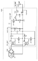
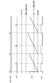
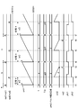
- the output timing correction circuit 113 does not output the set signal set2 at the generation timing of the zero current detection signal cd2, but outputs the set signal set2 after waiting until time t5.
- the PFC control pulse signal pfc2 is switched from the inactive level to the active level.
- the down counter 116 starts counting down from the pulse width setting value of the PFC control pulse signal pfc2.
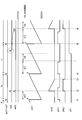
- the output timing correction circuit 113 does not output the set signal set2 in the cycle, and forcibly outputs the set signal set2 in the 1/2 cycle value T / 2 from the start of the next cycle. become.
- the error flag ef1 is switched from L to H at a timing exceeding the allowable period TR.
- each of the holding circuits HC1 to HC4 is composed of a D flip-flop.
- the SR in the previous stage indicates a set input and a reset input for the data input of the D flip-flop.
- a clock signal clk is input to the clock input of each D flip-flop.
- the determination period signal hs3 is changed from H to L.
- the hold signal hs4 changes from L to H and is held. Then, at the timing when the coincidence signal cs1 indicating the passage of the 1 ⁇ 2 period value T / 2 of the fourth period is input, the holding signal hs2 is changed from H to L, and the set signal set2c is output.
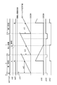
- FIG. 17 is a timing chart for explaining a method of generating the PFC control pulse signal pfc2, similarly to FIG.
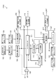
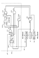
- the PFC signal generation unit PSG includes the output timing correction circuit 113.
- the output timing correction circuit 113 receives the zero current detection signal cd2 of the current I2 based on the set signal set1 for setting the PFC control pulse signal pfc1 to the active level and the coincidence signal cs1 output from the phase comparator 112.
- the set signal set2 for setting the PFC control pulse signal pfc2 to the active level is output at an appropriate timing.
- FIG. 18 is a block diagram of the PFC signal generation unit PSG according to the second embodiment.
- the PFC signal generation unit PSG shown in FIG. 18 has a period lower limit comparator 201 and a counter clear control circuit 202 added to the PFC signal generation unit PSG shown in FIG. In FIG. 18, the registers for storing the setting values are omitted.
- the output signal of the AND gate A11 is a detection signal s1 that is generated when the zero current detection signal cd1 of the current I1 is input below the cycle lower limit set value.
- This detection signal s1 is input to the set input S of the holding circuit HC12.
- the coincidence signal cs2 is input to the reset input R of the holding circuit HC12.
- the output signal of the holding circuit HC12 is a holding signal hs12 for holding up to the cycle lower limit set value when the zero current detection signal cd1 of the current I1 is input.
- the holding signal hs12 is input to one input of the AND gate A12.
- the coincidence signal cs2 is input to the other input of the AND gate A12.
- the output signal of the AND gate A12 is a clear signal cd1b that constitutes one of the set signals set1.
- the period signal hs11 output from the holding circuit HC11 is input to one input of the AND gate A13.
- the zero current detection signal cd1 of the current I1 is input to the other input of the AND gate A13.
- the output signal of the AND gate A13 is a clear signal cd1a that constitutes one of the set signals set1.
- the D flip-flop DF11 captures this and outputs an error flag ef2.
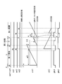
- the zero current detection signal cd1 of the current I1 is input below the cycle lower limit set value. Therefore, the zero current detection signal cd1 of the current I1 is input while the period signal hs11 indicating the period exceeding the cycle lower limit set value remains L. At that timing, the detection signal s1 is generated, and the hold signal hs12 is changed from L to H and held. Then, at the timing when the coincidence signal cs2 indicating the passage of the cycle lower limit set value is input, the holding signal hs12 is changed from H to L, and the clear signal cd1b is output.
- the cycle lower limit set value and guaranteeing the cycle lower limit of the PFC control pulse signal pfc1 it is possible to generate a PFC control pulse signal that further improves the power factor improvement by the PFC circuit.
Landscapes
- Engineering & Computer Science (AREA)
- Power Engineering (AREA)
- Dc-Dc Converters (AREA)
- Power Sources (AREA)
- Rectifiers (AREA)
Abstract
Description
特許文献1において、2つのコイル電流におけるゼロ電流をそれぞれ検出する場合、ノイズなどが原因で、おおよそπとなるべき2つのPFC制御パルス信号の位相差が小さくあるいは大きくなり過ぎるおそれがあった。そして、このような異常なPFC制御パルス信号により、電力ロスが増大し、力率が低下するおそれがあった。
まず、本実施の形態に係るPFC信号生成ユニットが適用されるプロセッサシステムの概要について説明する。なお、本実施の形態に係るPFC信号生成ユニットは、以下で説明するプロセッサシステムに適用されるものではあるが、説明するプロセッサシステムは一例であり、他のプロセッサシステムに本発明を適用することも可能である。
演算コアPEは、メモリMEMに格納されたプログラム又は外部から読み込んだプログラムに基づくプロセッサシステムMCUに求められる具体的な処理を行う。一般的には、CPU(Central Processing Unit)である。
クロック生成ユニットCGは、プロセッサシステムMCU内の各回路ブロックで利用されるクロック信号を生成する。また、クロック生成ユニットCGで生成されたクロック信号は、外部に出力されてもよい。
なお、プロセッサシステムMCU内で利用されるクロック信号は、外部の回路から供給することも可能である。
周期上限取込レジスタ103は、所定のタイミングで、周期上限設定レジスタ102から周期上限設定値を取り込む。
位相比較器112は、デジタルコンパレータであって、詳細には一致回路である。位相比較器112は、アップカウンタ101のカウント値cnt1と、シフト回路111が生成した1/2周期値T/2とが一致した場合、一致信号cs1を出力する。
まず、出力タイミング補正回路113は、各周期において、スタートから1/2周期値T/2(Tは前周期の周期値)の時間が経過するまでに、電流I2のゼロ電流検出信号cd2が発生したか否かを判定する(ステップST1)。スタートから1/2周期値T/2までの間に、電流I2のゼロ電流検出信号cd2が発生した場合(ステップST1YES)、出力タイミング補正回路113は、1/2周期値T/2まで待機して、セット信号set2を出力する(ステップST2)。ここで、目標位相差としては、T/2が最も好ましいのはいうまでもないが、3/8T~5/8Tであればよい。7/16T~9/16Tであれば、効率向上の観点から更に好ましい。
次に、図18を用いて、実施の形態2に係るPFC信号生成ユニットPSGについて説明する。図18は、実施の形態2に係るPFC信号生成ユニットPSGのブロック図である。図18に示すPFC信号生成ユニットPSGは、図6に示すPFC信号生成ユニットPSGに対し、周期下限比較器201、カウンタクリア制御回路202が付加されている。なお、図18においては、各設定値が格納されるレジスタは省略されている。
2 第2回路
3 第3回路
11 許容期間用ダウンカウンタ
101 アップカウンタ
102 周期上限設定レジスタ
103 周期上限取込レジスタ
104 周期上限比較器
105 第1パルス幅設定レジスタ
106 第1パルス幅取込レジスタ
107 パルス幅比較器
108 ORゲート
109 第1制御パルス出力回路
110 カウント値キャプチャ回路
111 シフト回路
112 位相比較器
113 出力タイミング補正回路
114 第2パルス幅設定レジスタ
115 第2パルス幅取込レジスタ
116 ダウンカウンタ
117 第2制御パルス出力回路
118 割込信号出力回路
201 周期下限比較器
202 カウンタクリア制御回路
A1-A5、A11-A13 ANDゲート
AP 交流電源
C1、C2 平滑コンデンサ
cd1、cd2 ゼロ電流検出信号
clr、cd1a、cd1b クリア信号
CG クロック生成ユニット
clk クロック信号
cnt1、cnt2、cnt3 カウント値
cs1、cs2 一致信号
D1-D3 ダイオード
DF1、DF11 Dフリップフロップ
ef1、ef2 エラーフラグ
fin カウント終了信号
FWR 全波整流回路
HC1-HC4、HC11、HC12 保持回路
hs1、hs11 期間信号
hs2、hs4、hs12 保持信号
hs3 判定期間信号
int 割込信号
IOU ユニット
L1、L11、L12、L2、L21、L22、L3 インダクタ
LED LED
Lm1、Lm2 モニタ用インダクタ
MCU プロセッサシステム
MEM メモリ
MON モニタユニット
mon、mon1-mon4 フィードバック信号
NM1-NM3 NMOSトランジスタ
O1、O2 ORゲート
PE 演算コア
PERI 周辺回路
pfc、pfc1、pfc2 PFC制御パルス信号
PSG PFC信号生成ユニット
PWM PWM信号生成ユニット
pwm PWM制御パルス信号
PWR 電源回路(制御対象回路)
R、R1、R2、Rm、Rm1、Rm2 抵抗
Claims (20)
- 第1のスイッチに接続された第1のインダクタと、第2のスイッチに接続された第2のインダクタと、を有するPFC回路を制御するPFC信号を生成するPFC信号生成回路であって、
前記第1のインダクタのゼロ電流検出タイミングで、前記第1のスイッチをオンする第1のPFC信号を出力する第1の制御信号出力回路と、
前記第2のインダクタのゼロ電流検出タイミングが、目標タイミングより早い場合、当該目標タイミングまで待機して前記第2のスイッチをオンにし、前記目標タイミングからの許容期間よりも遅い場合、次周期における前記目標タイミングで、前記第2のスイッチをオンする制御信号を生成するタイミング調整回路と、
前記制御信号に応じて、前記第2のスイッチをオンする第2のPFC信号を生成する第2の制御信号出力回路と、を備えるPFC信号生成回路。 - 前記第1のインダクタのゼロ電流検出タイミングで、カウント値がクリアされるカウンタを更に備えることを特徴とする請求項1に記載のPFC信号生成回路。
- 前記第1のインダクタのゼロ電流検出タイミングが、周期下限値を下回る場合、当該周期下限値まで待機してから前記カウンタ値をクリアするカウンタクリア制御回路を更に備える請求項2に記載のPFC信号生成回路。
- 前記カウンタの前周期における最大カウント値を取得するキャプチャ回路を更に備え、
前記目標タイミングが、前記最大カウント値から決定されることを特徴とする請求項2又は3に記載のPFC信号生成回路。 - 前記最大カウント値から前記目標タイミングの設定値を生成するシフト回路と、
前記目標タイミングの設定値と前記カウンタのカウント値を比較し、前記目標タイミングを生成する第1のデジタル比較器と、を更に備えることを特徴とする請求項4に記載のPFC信号生成回路。 - 前記目標タイミングが、前記最大カウント値の3/8~5/8であることを特徴とする請求項4又は5に記載のPFC信号生成回路。
- 前記許容期間が、前記最大カウント値の1/64~1/8であることを特徴とする請求項4~6のいずれか一項に記載のPFC信号生成回路。
- 前記PFC回路からのフィードバック信号に基づいて決定される前記第2のPFC信号のパルス幅の設定値をカウントダウンするダウンカウンタを更に備えることを特徴とする請求項1~7のいずれか一項に記載のPFC信号生成回路。
- 前記フィードバック信号に基づいて決定される前記第1のPFC信号のパルス幅の設定値と、前記カウンタのカウント値を比較する第2のデジタル比較器を更に備えることを特徴とする請求項8に記載のPFC信号生成回路。
- 前記タイミング調整回路は、
前記第2のインダクタのゼロ電流検出タイミングが、前記許容期間内である場合、当該第2のインダクタのゼロ電流検出タイミングで、前記第2のスイッチをオンする前記制御信号を生成することを特徴とする請求項1~9のいずれか一項に記載のPFC信号生成回路。 - 交流電源に接続されたPFC回路と、
前記PFC回路を制御するPFC信号を生成するPFC信号生成回路と、を備えたPFC制御システムであって、
前記PFC回路は、
第1のスイッチに接続された第1のインダクタと、
第2のスイッチに接続された第2のインダクタと、を備え、
前記PFC信号生成回路は、
前記第1のインダクタのゼロ電流検出タイミングで、前記第1のスイッチをオンする第1のPFC信号を出力する第1の制御信号出力回路と、
前記第2のインダクタのゼロ電流検出タイミングが、目標タイミングより早い場合、当該目標タイミングまで待機して前記第2のスイッチをオンにし、前記目標タイミングからの許容期間よりも遅い場合、次周期における前記目標タイミングで、前記第2のスイッチをオンする制御信号を生成するタイミング調整回路と、
前記制御信号に応じて、前記第2のスイッチをオンする第2のPFC信号を生成する第2の制御信号出力回路と、を備えるPFC制御システム。 - 前記PFC回路は、
前記第1のインダクタのゼロ電流検出タイミングで、カウント値がクリアされるカウンタを更に備えることを特徴とする請求項11に記載のPFC制御システム。 - 前記第1のインダクタのゼロ電流検出タイミングが、周期下限値を下回る場合、当該周期下限値まで待機してから前記カウンタ値をクリアするカウンタクリア制御回路を更に備える請求項12に記載のPFC制御システム。
- 前記PFC回路は、
前記カウンタの前周期における最大カウント値を取得するキャプチャ回路を更に備え、
前記目標タイミングが、前記最大カウント値から決定されることを特徴とする請求項12又は13に記載のPFC制御システム。 - 前記PFC回路は、
前記最大カウント値から前記目標タイミングの設定値を生成するシフト回路と、
前記目標タイミングの設定値と前記カウンタのカウント値を比較し、前記目標タイミングを生成する第1のデジタル比較器と、を更に備えることを特徴とする請求項14に記載のPFC制御システム。 - 前記PFC回路からのフィードバック信号に基づいて、前記第1及び第2のPFC信号のパルス幅を決定する演算回路を更に備えることを特徴とする請求項11~15のいずれか一項に記載のPFC制御システム。
- 前記PFC回路の出力電圧が供給されるDC/DCコンバータを更に備えることを特徴とする請求項11~16のいずれか一項に記載のPFC制御システム。
- 前記DC/DCコンバータの出力電圧が供給される発光ダイオードを更に備えることを特徴とする請求項17に記載のPFC制御システム。
- 第1のスイッチに接続された第1のインダクタと、第2のスイッチに接続された第2のインダクタと、を有するPFC回路を制御するPFC制御方法であって、
前記第1のインダクタのゼロ電流検出タイミングで、前記第1のスイッチをオンにし、
前記第2のインダクタのゼロ電流検出タイミングが、目標タイミングより早い場合、当該目標タイミングまで待機して前記第2のスイッチをオンにし、
前記目標タイミングからの許容期間よりも遅い場合、次周期における前記目標タイミングで、前記第2のスイッチをオンにするPFC制御方法。 - 前記第2のインダクタのゼロ電流検出タイミングが、前記許容期間内である場合、当該第2のインダクタのゼロ電流検出タイミングで、前記第2のスイッチをオンすることを特徴とする請求項19に記載のPFC制御方法。
Priority Applications (4)
| Application Number | Priority Date | Filing Date | Title |
|---|---|---|---|
| US14/113,612 US9614432B2 (en) | 2011-04-26 | 2012-04-04 | PFC signal generation circuit, PFC control system using the same, and PFC control method |
| CN201280020371.5A CN103503295B (zh) | 2011-04-26 | 2012-04-04 | Pfc信号生成电路、使用pfc信号生成电路的pfc控制系统以及pfc控制方法 |
| JP2013511897A JP5584826B2 (ja) | 2011-04-26 | 2012-04-04 | Pfc信号生成回路、それを用いたpfc制御システム、及びpfc制御方法 |
| US15/434,674 US10069404B2 (en) | 2011-04-26 | 2017-02-16 | PFC signal generation circuit, PFC control system using the same, and PFC control method |
Applications Claiming Priority (2)
| Application Number | Priority Date | Filing Date | Title |
|---|---|---|---|
| JP2011-098789 | 2011-04-26 | ||
| JP2011098789 | 2011-04-26 |
Related Child Applications (2)
| Application Number | Title | Priority Date | Filing Date |
|---|---|---|---|
| US14/113,612 A-371-Of-International US9614432B2 (en) | 2011-04-26 | 2012-04-04 | PFC signal generation circuit, PFC control system using the same, and PFC control method |
| US15/434,674 Continuation US10069404B2 (en) | 2011-04-26 | 2017-02-16 | PFC signal generation circuit, PFC control system using the same, and PFC control method |
Publications (1)
| Publication Number | Publication Date |
|---|---|
| WO2012147280A1 true WO2012147280A1 (ja) | 2012-11-01 |
Family
ID=47071814
Family Applications (1)
| Application Number | Title | Priority Date | Filing Date |
|---|---|---|---|
| PCT/JP2012/002341 Ceased WO2012147280A1 (ja) | 2011-04-26 | 2012-04-04 | Pfc信号生成回路、それを用いたpfc制御システム、及びpfc制御方法 |
Country Status (4)
| Country | Link |
|---|---|
| US (2) | US9614432B2 (ja) |
| JP (1) | JP5584826B2 (ja) |
| CN (1) | CN103503295B (ja) |
| WO (1) | WO2012147280A1 (ja) |
Cited By (2)
| Publication number | Priority date | Publication date | Assignee | Title |
|---|---|---|---|---|
| WO2025063297A1 (ja) * | 2023-09-20 | 2025-03-27 | 新電元工業株式会社 | 制御回路及びインターリーブ電源 |
| WO2025070317A1 (ja) * | 2023-09-29 | 2025-04-03 | 新電元工業株式会社 | 制御回路及びインターリーブ電源 |
Families Citing this family (12)
| Publication number | Priority date | Publication date | Assignee | Title |
|---|---|---|---|---|
| WO2012147286A1 (ja) | 2011-04-26 | 2012-11-01 | ルネサスエレクトロニクス株式会社 | Pfc信号生成回路、それを用いたpfc制御システム、及びpfc制御方法 |
| WO2012147280A1 (ja) * | 2011-04-26 | 2012-11-01 | ルネサスエレクトロニクス株式会社 | Pfc信号生成回路、それを用いたpfc制御システム、及びpfc制御方法 |
| CN205792228U (zh) * | 2015-03-17 | 2016-12-07 | 意法半导体股份有限公司 | 用于控制开关调节器的控制设备和电气装置 |
| CN106452045B (zh) * | 2016-10-10 | 2018-11-09 | 广州视源电子科技股份有限公司 | 交错pfc电路中pwm波形产生方法及装置 |
| JP2018153048A (ja) * | 2017-03-14 | 2018-09-27 | ルネサスエレクトロニクス株式会社 | スイッチングシステム |
| US10461654B2 (en) | 2017-05-04 | 2019-10-29 | Dell Products, Lp | Power supply light load efficiency control circuit |
| TWI674816B (zh) * | 2018-10-11 | 2019-10-11 | 茂達電子股份有限公司 | 低突波電流驅動電路和方法 |
| CN115765454A (zh) * | 2022-08-31 | 2023-03-07 | 广东工业大学 | 基于耦合电感的三相交错并联升降压变换器及其控制方法 |
| CN119731921A (zh) | 2022-10-04 | 2025-03-28 | 三星电子株式会社 | 用于供电的电子装置及其控制方法 |
| KR20240047225A (ko) * | 2022-10-04 | 2024-04-12 | 삼성전자주식회사 | 전원을 공급하기 위한 전자 장치 및 그 제어 방법 |
| CN118054658A (zh) * | 2022-11-15 | 2024-05-17 | 光宝科技股份有限公司 | 电源供应电路 |
| TWI835405B (zh) * | 2022-11-15 | 2024-03-11 | 光寶科技股份有限公司 | 電源供應電路 |
Citations (4)
| Publication number | Priority date | Publication date | Assignee | Title |
|---|---|---|---|---|
| JP2007195282A (ja) * | 2006-01-17 | 2007-08-02 | Renesas Technology Corp | 電源装置 |
| JP2010119285A (ja) * | 2008-10-16 | 2010-05-27 | Fuji Electric Systems Co Ltd | インターリーブ制御電源装置、該電源装置の制御回路および制御方法 |
| JP2010200437A (ja) * | 2009-02-24 | 2010-09-09 | Fuji Xerox Co Ltd | 電源装置 |
| JP2010233439A (ja) * | 2009-03-03 | 2010-10-14 | Toshiba Corp | 電源制御装置、及びそれを用いた電源装置 |
Family Cites Families (12)
| Publication number | Priority date | Publication date | Assignee | Title |
|---|---|---|---|---|
| JPH01293449A (ja) | 1988-05-23 | 1989-11-27 | Toshiba Corp | ウォッチドッグタイマ |
| GB9608832D0 (en) * | 1996-04-30 | 1996-07-03 | Switched Reluctance Drives Ltd | Power factor correction circuit |
| DE19942794A1 (de) * | 1999-09-08 | 2001-03-15 | Philips Corp Intellectual Pty | Konverter mit Hochsetzstelleranordnung |
| DE10042587B4 (de) * | 2000-08-30 | 2007-04-12 | Infineon Technologies Ag | Filteranordnung und Verfahren zur Filterung eines Analogsignals |
| CN101313632B (zh) * | 2005-12-12 | 2012-04-25 | 三菱电机株式会社 | 发光二极管照明装置和使用该装置的车辆用灯具照明装置 |
| JP2008068533A (ja) | 2006-09-14 | 2008-03-27 | Fujifilm Corp | 熱可塑性樹脂フィルムの縦延伸方法及びその方法で製造された縦延伸フィルム |
| WO2008032768A1 (en) * | 2006-09-14 | 2008-03-20 | Renesas Technology Corp. | Pfc controller, switching regulator and power supply circuit |
| US8432713B2 (en) | 2008-06-02 | 2013-04-30 | Dell Products, Lp | System and method for reducing an input current ripple in a boost converter |
| JP5326804B2 (ja) * | 2008-09-29 | 2013-10-30 | 富士電機株式会社 | 力率改善電源装置、該電源装置に用いられる制御回路および制御方法 |
| EP2270964B1 (en) * | 2009-07-03 | 2016-09-07 | Nxp B.V. | Method of controlling a power factor correction stage, a power factor correction stage and a controller therefor |
| JP4853568B2 (ja) * | 2009-11-12 | 2012-01-11 | ダイキン工業株式会社 | スイッチング電源回路 |
| WO2012147280A1 (ja) * | 2011-04-26 | 2012-11-01 | ルネサスエレクトロニクス株式会社 | Pfc信号生成回路、それを用いたpfc制御システム、及びpfc制御方法 |
-
2012
- 2012-04-04 WO PCT/JP2012/002341 patent/WO2012147280A1/ja not_active Ceased
- 2012-04-04 CN CN201280020371.5A patent/CN103503295B/zh active Active
- 2012-04-04 US US14/113,612 patent/US9614432B2/en active Active
- 2012-04-04 JP JP2013511897A patent/JP5584826B2/ja active Active
-
2017
- 2017-02-16 US US15/434,674 patent/US10069404B2/en active Active
Patent Citations (4)
| Publication number | Priority date | Publication date | Assignee | Title |
|---|---|---|---|---|
| JP2007195282A (ja) * | 2006-01-17 | 2007-08-02 | Renesas Technology Corp | 電源装置 |
| JP2010119285A (ja) * | 2008-10-16 | 2010-05-27 | Fuji Electric Systems Co Ltd | インターリーブ制御電源装置、該電源装置の制御回路および制御方法 |
| JP2010200437A (ja) * | 2009-02-24 | 2010-09-09 | Fuji Xerox Co Ltd | 電源装置 |
| JP2010233439A (ja) * | 2009-03-03 | 2010-10-14 | Toshiba Corp | 電源制御装置、及びそれを用いた電源装置 |
Cited By (2)
| Publication number | Priority date | Publication date | Assignee | Title |
|---|---|---|---|---|
| WO2025063297A1 (ja) * | 2023-09-20 | 2025-03-27 | 新電元工業株式会社 | 制御回路及びインターリーブ電源 |
| WO2025070317A1 (ja) * | 2023-09-29 | 2025-04-03 | 新電元工業株式会社 | 制御回路及びインターリーブ電源 |
Also Published As
| Publication number | Publication date |
|---|---|
| US10069404B2 (en) | 2018-09-04 |
| US20170163149A1 (en) | 2017-06-08 |
| CN103503295A (zh) | 2014-01-08 |
| US20140042992A1 (en) | 2014-02-13 |
| JP5584826B2 (ja) | 2014-09-03 |
| US9614432B2 (en) | 2017-04-04 |
| JPWO2012147280A1 (ja) | 2014-07-28 |
| CN103503295B (zh) | 2016-03-09 |
Similar Documents
| Publication | Publication Date | Title |
|---|---|---|
| JP5584826B2 (ja) | Pfc信号生成回路、それを用いたpfc制御システム、及びpfc制御方法 | |
| JP5584827B2 (ja) | Pfc信号生成回路、それを用いたpfc制御システム、及びpfc制御方法 | |
| CN102148569B (zh) | 用于控制具有低回路带宽的功率转换器的方法和设备 | |
| CN103493349B (zh) | Pwm信号生成电路和处理器系统 | |
| CN105611686B (zh) | Led驱动方法和led驱动装置 | |
| CN101546961B (zh) | 降低了谐波电流的ac到dc电力变换方法和装置 | |
| TWI489762B (zh) | High efficiency AC - DC voltage conversion circuit | |
| JP2012203866A (ja) | クロック生成回路、それを用いたプロセッサシステム、及びクロック周波数制御方法 | |
| CN109245055B (zh) | 功率变换系统、功率开关管的过流保护电路及方法 | |
| US20160344282A1 (en) | Power factor correction control device for dynamically sensing and boost regulation | |
| CN103138584B (zh) | 车载低电压直流电源转换装置 | |
| JP2009148149A (ja) | 昇降圧チョッパ回路の制御方法 | |
| WO2014032429A1 (zh) | 一种带功率因数校正的恒流控制电路及方法 | |
| CN110661439A (zh) | 一种降低数字开关电源纹波的装置及方法 | |
| CN102892239B (zh) | 反激式恒流驱动电路及包含其的反激式恒流驱动控制系统 | |
| CN101800528A (zh) | 一种扩展控制器pwm分辨率的方法及装置 | |
| CN102447390A (zh) | 多相控制系统及控制单元 | |
| CN102468792B (zh) | 风扇用直流无刷马达的驱动装置 | |
| CN104702092A (zh) | 电源转换器的功率因数校正电路 | |
| JP2008312278A (ja) | 電力変換装置 | |
| CN113992011A (zh) | 多相开关变换器级联系统及其电压变换电路 | |
| WO2022083139A1 (zh) | 数字处理设备的算力板、供电系统和数字处理设备 | |
| CN214900683U (zh) | 一种电动工具用开关电源电路 | |
| CN204335078U (zh) | 一种led驱动电路 | |
| KR20170021943A (ko) | 전원 공급부 및 그의 구동방법 |
Legal Events
| Date | Code | Title | Description |
|---|---|---|---|
| WWE | Wipo information: entry into national phase |
Ref document number: 201280020371.5 Country of ref document: CN |
|
| 121 | Ep: the epo has been informed by wipo that ep was designated in this application |
Ref document number: 12776840 Country of ref document: EP Kind code of ref document: A1 |
|
| ENP | Entry into the national phase |
Ref document number: 2013511897 Country of ref document: JP Kind code of ref document: A |
|
| WWE | Wipo information: entry into national phase |
Ref document number: 14113612 Country of ref document: US |
|
| NENP | Non-entry into the national phase |
Ref country code: DE |
|
| 122 | Ep: pct application non-entry in european phase |
Ref document number: 12776840 Country of ref document: EP Kind code of ref document: A1 |