WO2012141203A1 - 検査装置、検査システム及び検査方法 - Google Patents
検査装置、検査システム及び検査方法 Download PDFInfo
- Publication number
- WO2012141203A1 WO2012141203A1 PCT/JP2012/059882 JP2012059882W WO2012141203A1 WO 2012141203 A1 WO2012141203 A1 WO 2012141203A1 JP 2012059882 W JP2012059882 W JP 2012059882W WO 2012141203 A1 WO2012141203 A1 WO 2012141203A1
- Authority
- WO
- WIPO (PCT)
- Prior art keywords
- inspection
- test
- cell
- test pattern
- memory
- Prior art date
- Legal status (The legal status is an assumption and is not a legal conclusion. Google has not performed a legal analysis and makes no representation as to the accuracy of the status listed.)
- Ceased
Links
Images






Classifications
-
- G—PHYSICS
- G01—MEASURING; TESTING
- G01R—MEASURING ELECTRIC VARIABLES; MEASURING MAGNETIC VARIABLES
- G01R31/00—Arrangements for testing electric properties; Arrangements for locating electric faults; Arrangements for electrical testing characterised by what is being tested not provided for elsewhere
- G01R31/28—Testing of electronic circuits, e.g. by signal tracer
- G01R31/317—Testing of digital circuits
- G01R31/3181—Functional testing
- G01R31/319—Tester hardware, i.e. output processing circuits
- G01R31/31917—Stimuli generation or application of test patterns to the device under test [DUT]
- G01R31/31919—Storing and outputting test patterns
-
- G—PHYSICS
- G01—MEASURING; TESTING
- G01R—MEASURING ELECTRIC VARIABLES; MEASURING MAGNETIC VARIABLES
- G01R31/00—Arrangements for testing electric properties; Arrangements for locating electric faults; Arrangements for electrical testing characterised by what is being tested not provided for elsewhere
- G01R31/26—Testing of individual semiconductor devices
-
- G—PHYSICS
- G01—MEASURING; TESTING
- G01R—MEASURING ELECTRIC VARIABLES; MEASURING MAGNETIC VARIABLES
- G01R31/00—Arrangements for testing electric properties; Arrangements for locating electric faults; Arrangements for electrical testing characterised by what is being tested not provided for elsewhere
- G01R31/28—Testing of electronic circuits, e.g. by signal tracer
- G01R31/2851—Testing of integrated circuits [IC]
- G01R31/2886—Features relating to contacting the IC under test, e.g. probe heads; chucks
- G01R31/2889—Interfaces, e.g. between probe and tester
-
- G—PHYSICS
- G01—MEASURING; TESTING
- G01R—MEASURING ELECTRIC VARIABLES; MEASURING MAGNETIC VARIABLES
- G01R31/00—Arrangements for testing electric properties; Arrangements for locating electric faults; Arrangements for electrical testing characterised by what is being tested not provided for elsewhere
- G01R31/28—Testing of electronic circuits, e.g. by signal tracer
- G01R31/317—Testing of digital circuits
- G01R31/3181—Functional testing
- G01R31/319—Tester hardware, i.e. output processing circuits
- G01R31/3193—Tester hardware, i.e. output processing circuits with comparison between actual response and known fault free response
- G01R31/31932—Comparators
-
- G—PHYSICS
- G01—MEASURING; TESTING
- G01R—MEASURING ELECTRIC VARIABLES; MEASURING MAGNETIC VARIABLES
- G01R31/00—Arrangements for testing electric properties; Arrangements for locating electric faults; Arrangements for electrical testing characterised by what is being tested not provided for elsewhere
- G01R31/28—Testing of electronic circuits, e.g. by signal tracer
- G01R31/317—Testing of digital circuits
- G01R31/3181—Functional testing
- G01R31/319—Tester hardware, i.e. output processing circuits
- G01R31/3193—Tester hardware, i.e. output processing circuits with comparison between actual response and known fault free response
- G01R31/31935—Storing data, e.g. failure memory
-
- H—ELECTRICITY
- H10—SEMICONDUCTOR DEVICES; ELECTRIC SOLID-STATE DEVICES NOT OTHERWISE PROVIDED FOR
- H10P—GENERIC PROCESSES OR APPARATUS FOR THE MANUFACTURE OR TREATMENT OF DEVICES COVERED BY CLASS H10
- H10P74/00—Testing or measuring during manufacture or treatment of wafers, substrates or devices
-
- H—ELECTRICITY
- H10—SEMICONDUCTOR DEVICES; ELECTRIC SOLID-STATE DEVICES NOT OTHERWISE PROVIDED FOR
- H10P—GENERIC PROCESSES OR APPARATUS FOR THE MANUFACTURE OR TREATMENT OF DEVICES COVERED BY CLASS H10
- H10P74/00—Testing or measuring during manufacture or treatment of wafers, substrates or devices
- H10P74/27—Structural arrangements therefor
- H10P74/273—Interconnections for measuring or testing, e.g. probe pads
Definitions
- the disclosed technology of this specification relates to an inspection apparatus, an inspection system, and an inspection method for inspecting a plurality of inspected objects.
- inspection of electrical characteristics of a device formed on a semiconductor wafer is performed using, for example, a probe card or a tester mounted on a probe apparatus.
- the probe card normally includes a plurality of probes, a contactor that supports the probes, a circuit board that transmits an inspection signal to each probe, and the like.
- the tester also includes a driver for transmitting an inspection signal to the probe card, a comparator for comparing an output signal from the probe card and an expected value, and the like.
- the electrical characteristics of the device are inspected by bringing a plurality of probes into contact with the electrodes of the device formed on the wafer, and sending inspection signals from the tester driver to the device on the wafer through the circuit board, contactor, and probe. To do. Further, an output signal is transmitted from the device to the tester comparator through the probe, contactor, and circuit board. The comparator compares the output signal with the expected value and inspects the electrical characteristics of the device.
- the tester when the tester is provided with a driver and a comparator, the wiring length connecting the tester and the probe card increases. As a result, the resistance of the wiring may increase or the wiring delay may increase. In such a case, since the signal cannot be properly transmitted between the tester and the probe card, the inspection accuracy of the device deteriorates or the inspection speed decreases.
- Patent Document 1 proposes a comparator provided in a conventional tester in the vicinity of a device to be inspected.
- the disclosed technology of the present specification has been made in view of such a point, and aims to easily and appropriately inspect a plurality of objects to be inspected.
- the disclosed technique of the present specification is an inspection apparatus for inspecting a plurality of objects to be inspected, and includes a plurality of inspection cells provided corresponding to the objects to be inspected. Includes a test pattern memory that temporarily holds a test pattern, a driver that transmits an inspection signal to an object to be inspected according to the test pattern, an output signal from the object to be inspected, and an expected value corresponding to the test pattern. A comparator for deriving a test result by comparison; and a test result memory for temporarily holding the test result, and the test of the inspection cell upstream in the order of inspection of the object to be inspected is provided between the inspection cells. Test pattern wiring for transmitting the test pattern from the pattern memory to the test pattern memory of the inspection cell downstream is provided.
- the inspection cell since the inspection cell includes a test pattern memory, a driver, a comparator, and a test result memory, the inspection cell is arranged in the vicinity of the inspection object and the inspection object is inspected. be able to. Therefore, the distance for transmitting a signal between the driver and comparator of the inspection cell and the object to be inspected is shortened. For this reason, while being able to improve the test
- test pattern wiring is provided between the test cells, the test pattern held in the test pattern memory of one test cell is changed to the test pattern of the test cell downstream of the one test cell. Can be sent sequentially to the memory. That is, if a test pattern is transmitted from the outside of the inspection apparatus (for example, a tester) to the test pattern memory of the inspection cell on the most upstream side, a plurality of inspected objects can be inspected sequentially. Therefore, it is not necessary to individually transmit a signal from the tester to each object to be inspected as in the prior art, and the wiring length for transmitting the signal does not vary. For this reason, the inspection accuracy of the object to be inspected can be improved.
- test pattern can be sequentially transmitted to the test pattern memory of the inspection cell in this way, the test pattern is sequentially rewritten in the test pattern memory. For this reason, even when inspecting an object to be inspected with a plurality of test patterns, the test pattern memory only needs to hold the test pattern performed in the inspection cell. Therefore, it is possible to inspect an object to be inspected according to a plurality of test patterns with a simple configuration. Further, in this case, since the inspection cell can be configured simply, the inspection cell can be further arranged in the vicinity of the inspection object, which is particularly useful when the number of inspection objects is large.
- the inspection object can be inspected with simpler control than before. . Further, due to such simple control, the inspection speed of the object to be inspected can be further improved. As described above, according to the disclosed technique of the present specification, it is possible to easily and appropriately inspect a plurality of objects to be inspected.
- the disclosed technology of the present specification is an inspection system including an inspection apparatus that inspects a plurality of objects to be inspected, and the inspection apparatus includes a plurality of inspection cells provided corresponding to the objects to be inspected.
- the test cell includes a test pattern memory that temporarily holds a test pattern, a driver that transmits an inspection signal to the object to be inspected according to the test pattern, an output signal from the object to be inspected, and the test pattern.
- the inspection system includes a tester that transmits the test pattern to the test pattern memory and receives the test result from the test result memory, and a control unit that controls inspection of an object to be inspected in the inspection apparatus.
- the disclosed technology of the present specification is an inspection method for inspecting a plurality of objects to be inspected, and a test pattern memory for temporarily holding a test pattern, and inspecting the object to be inspected according to the test patterns
- a driver for transmitting a signal, a comparator for deriving a test result by comparing an output signal from the device under test with an expected value corresponding to the test pattern, a test result memory for temporarily holding the test result, And a test pattern memory of the test cell on the downstream side of the one test cell, the test cell having a test pattern stored in the test pattern memory of the one test cell.
- the test object is inspected according to the transmitted test pattern in each test cell, and a plurality of test objects are sequentially inspected.
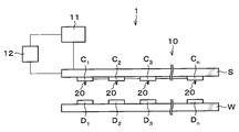
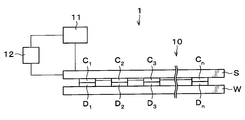
- FIG. 1 is an explanatory diagram showing a configuration of an inspection system 1 according to the present embodiment.
- the inspection system 1 inspects a plurality of devices D as inspection objects formed on the wafer W.
- the device D inspection a case will be described in which a dynamic characteristic inspection of the device D, for example, a function test for inspecting the operation and operation speed of the device D is performed.
- the inspection system 1 includes an inspection device 10 and a tester 11 as shown in FIG.
- the tester 11 transmits a test pattern to the inspection apparatus 10 and receives a test result from the inspection apparatus 10.
- the inspection system 1 includes a control unit 12 that controls the inspection apparatus 10 and the tester 11 in order to control inspection of a plurality of devices D, for example.
- the inspection system 1 includes a chuck that holds the wafer W by suction, a moving mechanism that moves the chuck in the vertical direction and the horizontal direction, and the like.
- the inspection apparatus 10 has a plurality of inspection cells C.
- the plurality of inspection cells C are supported by a support substrate S, for example.
- the support substrate S is made of the same material as the wafer W, for example, and has the same planar shape as the wafer W.
- Each inspection cell C is provided with a probe 20 in contact with the electrode of the device D. That is, the inspection cell C and the probe 20 are provided in a one-to-one correspondence.
- the material and shape of the support substrate S are not limited to the present embodiment, and various materials and shapes can be used as long as the substrate can support a plurality of inspection cells C.
- the plurality of inspection cells C are provided corresponding to the plurality of devices D on the wafer W, respectively.
- a test cell C of the n inspection apparatus 10 (n is an integer of 2 or more), the inspection cell of the n respective test cell C from the first test cell C 1 it may be referred to as C n.
- each device D formed on the wafer W from the first device D 1 is referred to as a device D n of the n.
- the device D n of the test cell C n and the n from a first device D 1 of the first n from the first test cell C 1 is provided in each one-to-one correspondence.
- the device D n of the n from the first device D 1 is examined in this order from each of the first test cell C 1 by the inspection cell C n of the n.
- a plurality of devices D on the wafer W and a plurality of inspection cells C in the inspection apparatus 10 can be arbitrarily arranged.
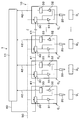
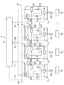
- the inspection cell C includes a test pattern memory 30, a driver 31, a comparator 32, and a test result memory 33.
- the test pattern memory 30 temporarily holds the test pattern transmitted from the tester 11.
- the test pattern memory 30 which receives a test pattern from the tester 11 as described later, only the test pattern memory 30 in the first test cell C 1.
- the test pattern (including the expected value corresponding to the test pattern) held in the test pattern memory 30 is transmitted to the driver 31 and the comparator 32.
- the driver 31 transmits an inspection signal to the device D via the probe 20 according to the test pattern from the test pattern memory 30.
- the comparator 32 compares the output signal from the device D with the expected value corresponding to the test pattern from the test pattern memory 30 and derives the test result, that is, “Pass” or “Fail”.
- the test result derived by the comparator 32 is transmitted to the test result memory 33.
- the test result memory 33 temporarily holds the test result from the comparator 32.
- the inspection signal from the driver 31 is output with high impedance.
- the switch which switches the driver 31 and the comparator 32 is not provided.
- the switch may be provided between the driver 31 and the comparator 32 and the probe 20.
- a wiring 40 for transmitting a test pattern (including an expected value corresponding to the test pattern) is provided.
- a test pattern wiring 41 for transmitting a test pattern is provided between adjacent inspection cells C and C.
- the test pattern wiring 41 connects the test pattern memories 30 and 30 in the adjacent inspection cells C and C.
- the inter-test cells adjacent C, C for example, the first test cell C 1 and or between the second test cell C 2, a second test cell C 2 and the third test cell C 2
- the adjacent inspection cells C and C are not limited to the adjacent inspection cells C and C in physical arrangement in plan view.
- test pattern is transmitted from the tester 11 to the test pattern memory 30 of the first inspection cell C 1 on the most upstream side, and further the nth inspection on the most downstream side from the test pattern memory 30 of the first inspection cell C 1. the test pattern memory 30 of the cell C n so that the test pattern is sequentially transmitted.
- wirings 42 for transmitting the test results are provided. Then, the test results held in the test result memory 33 of each inspection cell C are individually transmitted to the tester 11 via the wiring 42.
- a clock wiring 50 for transmitting a clock signal is connected to the test pattern memory 30 of each inspection cell C.
- the clock signal wiring 50 is connected to a clock signal generator (not shown).
- the test pattern held in the test pattern memory 30 is rewritten in synchronization with the clock signal transmitted from the clock wiring 50.
- the 1 is a computer, for example, and has a program storage unit (not shown).
- the program storage unit stores a program for controlling the inspection of a plurality of devices D by controlling transmission / reception of each signal between the inspection apparatus 10 and the tester 11.
- the program is recorded on a computer-readable storage medium such as a computer-readable hard disk (HD), flexible disk (FD), compact disk (CD), magnetic optical desk (MO), or memory card. Or installed in the control unit 12 from the storage medium.
- a computer-readable storage medium such as a computer-readable hard disk (HD), flexible disk (FD), compact disk (CD), magnetic optical desk (MO), or memory card.
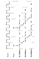
- FIG. 3 is an explanatory diagram showing the timing for inspecting a plurality of devices D by the inspection system 1.
- the irregularities of the clock indicate the pulses of the clock signal.
- TP is an abbreviation for Test Pattern.
- TR is an abbreviation for Test Result.
- “1” in “TP1” and “TR1” indicates the first inspection
- “2” in “TP2” and “TR2” indicates the second inspection.
- the third device D 3 illustrates a case where the first device D 1 to the third device D 3 are sequentially inspected by the first inspection cell C 1 to the third inspection cell C 3 .
- the first device D 1 to the n-th device D n are sequentially inspected by the first to n- th inspection cells C 1 to C n .
- the wafer W is moved in the horizontal direction, and the wafer W is disposed facing the inspection apparatus 10. That is, each device D on the wafer W and each inspection cell C of the inspection apparatus 10 are arranged to face each other. Thereafter, the wafer W is moved in the vertical direction, and the probes 20 of the inspection apparatus 10 are brought into contact with the electrodes of the devices D on the wafer W.
- a test pattern is transmitted from the tester 11 to the test pattern memory 30 of the first inspection cell C 1 , and the test pattern is temporarily held in the test pattern memory 30.
- the first device D 1 is tested in synchronization with the clock signal transmitted to the test pattern memory 30.
- the test pattern held in the test pattern memory 30 (including an expected value corresponding to the test pattern), is transmitted to the driver 31 and the comparator 32 in synchronization clock signal.
- the test pattern memory 30 the test pattern is rewritten in synchronization with the clock signal.
- an inspection signal is transmitted to the first device D 1 through the probe 20 according to the test pattern from the test pattern memory 30. Based on this inspection signal, an output signal is transmitted from the first device D 1 to the comparator 32.
- the comparator 32 compares the expected value corresponding to the test pattern from the output signal and the test pattern memory 30 from the first device D 1, the test result is derived.
- the test result derived by the comparator 32 is transmitted to the test result memory 33.
- the test result memory 33 temporarily holds the test result from the comparator 32.
- the test result held in the test result memory 33 is transmitted to the tester 11.
- the first device D 1 is inspected by the first inspection cell C 1 .
- a test pattern to the test pattern memory 30 from the first test pattern memory 30 of the inspection cell C 1 second inspection cell C 2 is Sent.
- the test pattern is temporarily held in the second test pattern memory 30 of the inspection cell C 2.
- the second device D 2 is inspected according to the test pattern in the test pattern memory 30. Incidentally, the inspection of the second device D 2 is omitted because it is similar to the test of the first device D 1 described above.
- test pattern is sequentially transmitted from the first test pattern memory 30 of the inspection cell C 1 to the test pattern memory 30 of the inspection cell C n of the n.
- the device D is inspected according to the test pattern held in the test pattern memory 30 of the inspection cell C.
- the inspection system 1, the device D n of the n is sequentially inspected from the first device D 1.
- each device D is inspected a plurality of times according to a plurality of test patterns.
- FIG. 3 the case where the inspection of the device D is performed twice by each inspection cell C is shown, but the number of inspections of the device D can be arbitrarily set.
- the inspection cell C since the inspection cell C includes the test pattern memory 30, the driver 31, the comparator 32, and the test result memory 33, the inspection cell C is arranged in the vicinity of the device D, and the device D Can be inspected. Accordingly, the distance for transmitting signals between the driver 31 and the comparator 32 of the inspection cell C and the device D is shortened. If the transmission distance is shortened in this way, the rounding of the signal waveform (rise and fall) is suppressed, and the signal is transmitted with good reproducibility, so that the transmission frequency can be increased.
- the transmission frequency of the signal performed between the driver 31 and the comparator 32 of the inspection cell C and the device D depends on the response speed of the device D, if the present embodiment is used, an inspection with a high frequency is performed. The system can be designed easily.
- Each test cell C since the test pattern wiring 41 between C are provided, the test pattern, the test pattern of the test cell C n of the n from the first test pattern memory 30 of the inspection cell C 1
- the data are sequentially transmitted to the memory 30. That is, it is possible if it is the first test cell C 1 in the test pattern memory 30 to the test pattern of the most upstream side is transmitted from the tester 11 sequentially examines the device D n of the n from a first device D 1 . Therefore, it is not necessary to individually transmit a signal from the tester to each device as in the conventional case, and the wiring length for transmitting the signal does not vary. For this reason, the inspection accuracy of the device D can be improved.
- test patterns can be sequentially transmitted to the test pattern memory 30 of the inspection cell C in this way, the test patterns are sequentially rewritten in the test pattern memory 30. Therefore, even when the device D is inspected with a plurality of test patterns, the test pattern memory 30 only needs to hold the test pattern being performed in the inspection cell C. Therefore, the inspection of the device D according to a plurality of test patterns can be performed with a simple configuration. Further, in this case, since the inspection cell C can be configured simply, the inspection cell C can be further arranged in the vicinity of the device D, which is particularly useful when the number of devices D on the wafer W is large.
- the device D is inspected with simpler control than before. Can do. Further, due to such simple control, the inspection speed of the device D can be further improved.
- test pattern memory 30 of each inspection cell C the test pattern is rewritten in synchronization with the clock signal, so that the device D can be inspected at an appropriate timing.
- the rewriting of the test pattern in the test pattern memory 30 and the transmission of the test result from the test result memory 33 to the tester 11 are transmitted from the clock wiring 50.
- the rewriting of the test pattern and the transmission of the test result may be performed at different timings. For example, when the cycle of the clock signal and the test speed in the test cell C are different, the test pattern is rewritten in the test pattern memory 30 in synchronization with the clock signal, and the test result is transferred to the tester 11 in the test result memory 33 in synchronization with the test speed. It may be transmitted.
- the test pattern in the test pattern memory 30 is rewritten at the rising edge of the clock signal, the clock signal is lowered at the timing matched with the test speed, for example, and the test result is transmitted from the test result memory 33 to the tester 11. May be.
- the test cell C can include a cache capable of absorbing the difference between the clock signal cycle and the test speed.
- the tester 11 and the test result memory 33 of each test cell C are connected by the individual wiring 42.
- the wiring 60 may be connected. Then, from the first test cell C 1 to the inspection cell C n of the n, successively test result from the test result memory 33 to the tester 11 is transmitted. In such a case, it is not necessary to provide a plurality of wirings for outputting test results between the tester 11 and the inspection apparatus 10, so that the configuration of the inspection system 1 can be simplified.
- the wiring 40 that connects the tester 11 and the test pattern 30 and the wiring 60 that connects the tester 11 and each test result memory 33 may be combined into a single wiring.
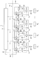
- each test cell C has a switch 70 as shown in FIG. Between the switch 70 and the tester 11, a DC test wiring for transmitting an inspection signal for performing a DC test from the tester 11 to the device D and transmitting an output signal (test result) from the device D to the tester 11. 71 is provided.
- the switch 70 can switch between an inspection signal from the driver 31 for performing a function test of the device D and an output signal to the comparator 32 and a signal for performing a DC test of the device D.
- the device D is inspected at the timing shown in FIG. That is, in each inspection cell C, a function test of the device D is first performed. Since this function test is the same as that in the above embodiment, the description thereof is omitted. Thereafter, the switch 70 is switched to the DC test wiring 71 side, and a test signal for DC test is transmitted from the tester 11 to the device D. Based on this inspection signal, an output signal (test result) is transmitted from the device D to the tester 11. In this way, the DC test of the device D is performed.
- a test pattern is sequentially transmitted from the first test pattern memory 30 of the inspection cell C 1 to the test pattern memory 30 of the inspection cell C n of the n. Then, the device D n of the n from the first device D 1, function test and the DC test is performed sequentially.
- the inspection of the device D can be performed efficiently.
- a test result wiring 80 for transmitting a test result may be provided between adjacent inspection cells C and C.
- the test result wiring 80 connects the test result memories 33 and 33 in the adjacent inspection cells C and C.
- between the adjacent inspection cells C and C refers to the space between the upstream inspection cell C and the downstream inspection cell C in the inspection order of the device D as described above.
- a wiring 81 for transmitting a test result is provided between the tester 11 and the test result memory 33 of the nth test cell Cn.
- the device D is inspected at the timing shown in FIG. That is, in each inspection cell C, a function test and a DC test of the device D are performed. Since the function test and DC test of the device D are the same as those in the above embodiment, the description thereof is omitted.
- a method of transmitting the test result stored in the test result memory 33 of the test cell C to the tester 11 after the function test in each test cell C will be described.
- test result for the first device D 1 held in the test result memory 33 of the first test cell C 1 is transmitted to the test result memory 33 of the second test cell C 2 .
- the inspection of the second device D 2 is completed in the second inspection cell C 2 , and the test result for the second device D 2 is held in the test result memory 33.
- the test result memory 33 of the second inspection cell C 2 if both the test result of the first device D 1 and the test result of the second device D 2 are “Pass”, the test result is “Pass”. It becomes.
- the test result of the first device D 1 or the test result of the second device D 2 is “Fail”, the test result is “Fail”. Then, the test results are sequentially transmitted from the test result memory 33 of the first test cell C 1 to the test result memory 33 of the nth test cell C n .
- one test result is derived for the plurality of devices D as a whole. That is, if the test result of the plurality of devices D is all "Pass”, "Pass” is held in the test result memory 33 of the inspection cell C n of the n as the test result. On the other hand, if any one of the test results of the plurality of devices D is “Fail”, “Fail” is held as the test result.
- the test cell C n test results test results held in the memory 33 of the n-th is transmitted to the tester 11 via the lines 81.
- the test result from the inspection apparatus 10 is transmitted via the single wiring 81. Therefore, it is not necessary to individually transmit a signal from each device to the tester as in the prior art, and the wiring length for transmitting the signal does not vary. For this reason, the inspection accuracy of the device D can be further improved.
- the device D is inspected with simpler control than before. Can do. Further, due to such simple control, the inspection speed of the device D can be further improved.
- rewriting of the test pattern in the test pattern 30 of each inspection cell C, transmission of the test result from the upstream side to the downstream inspection cell C, and the tester from the nth inspection cell C n may be performed in synchronization with the clock signal transmitted from the clock wiring 50, or may be performed at a different timing. That is, for example, in the test pattern memory 30, the test pattern is rewritten in synchronization with the clock signal.
- the transmission of the test result from the test result memory 33 of the upstream inspection cell C to the test result memory 33 of the downstream inspection cell C and the test result from the test result memory 33 of the most downstream n-th inspection cell C n is transmitted in synchronization with the test speed.
- the tester 11 and the inspection apparatus 12 are connected by the individual wires 40 and 81, but may be connected by a single wire 90 as shown in FIG.
- a test pattern from the tester 11 to the first inspection cell C 1 and the test results to the tester 11 from the test cell C n of the n, and transmitted by a single wire 90.
- the configuration of the inspection system 1 can be simplified.
- test pattern and the expected value corresponding to the test pattern are sequentially transmitted from the tester 11 to the test pattern memory 30 of the first test cell C 1.
- the test pattern memory 30 of the cell C 1 even when transmitting only the test pattern can be applied to the technique disclosed herein.
- test result memory 33 of the first test cell C 1 and the test pattern memory 30 of the second test cell C 2 are connected by a wiring 100.
- the first inspection cell C 1 When inspecting the plurality of devices D, first, in the first inspection cell C 1 , an inspection signal is transmitted to the first device D 1 according to the test pattern transmitted from the tester 11, and the first device D 1 An output signal from the device D 1 is output to the test result memory 33. At this time, since the expected value corresponding to the test pattern from the tester 11 is not being transmitted, the comparator 32, the expected value corresponding to the output signal and the test pattern from the first device D 1 as in the above embodiment Is not compared. The output signal from the first device D 1 is, in the testing cell C 2 ⁇ C n of the first downstream side of the inspection cell C 1, the expected value corresponding to the test pattern.
- a test pattern is transmitted from the test pattern memory 30 of the first test cell C 1 to the test pattern memory 30 of the second test cell C 2 , and the test result of the first test cell C 1
- An output signal from the first device D 1 is transmitted from the memory 33.
- the test pattern held in the test pattern memory 30 and the output signal from the first device D 1 are transmitted to the driver 31 and the comparator 32.
- an inspection signal is transmitted to the second device D 2 via the probe 20 according to the test pattern from the test pattern memory 30.
- the output signal is transmitted from the second device D 2 to the comparator 32.
- the comparator 32 compares the output signal from the first device D 1 of the output signal from the test pattern memory 30 from the second device D 2, these output signals are identical whether the test results Derived.
- the test result derived by the comparator 32 is transmitted to the test result memory 33.
- the test result memory 33 temporarily holds the test result from the comparator 32.
- the test result held in the test result memory 33 is transmitted to the tester 11.
- the second device D 2 is inspected by the second inspection cell C 2.
- the test pattern and the output signal from the first device D 1 is sequentially transmitted from the second test pattern memory 30 of the inspection cell C 2 in the test pattern memory 30 of the inspection cell C n of the n.
- the device D is inspected according to the test pattern held in the test pattern memory 30 of the inspection cell C and the output signal from the first device D1.
- the inspection system 1, the device D n of the n are sequentially examined from the second device D 2.
- the device D n of the n from a second device D 2 is examined in turn Is done. That is, the output signal from the device D n of the n from a second device D 2 Whether the comparison test matches the first output signal from the device D 1 is performed. Then, for example, it is expected value corresponding to the test pattern even if it is not derived in advance, it is possible from a first device D 1 performs a comparison test in the device D n of the n.
- the defect rate of the device D is generally low at the mass production stage of the product. Therefore, it is effective for detection of defective devices D to the first device D 1 as in this embodiment comparison inspection device D n of the n.
- a series of test cells C multiple sets from the first test cell C 1, as shown in FIG. 11 to the inspection cell C n of the n for example, m sets (m is 2 (Integer above) may be provided. That is, for example, the first test cell C 1 is more, for example may be provided m pieces.
- the first test cell C 1 of the plurality constitutes a first test chip P 1.
- test cell C n of the plurality of first n constitute a test chip P n of the n.
- Each inspection chip P is provided corresponding to a chip formed by a plurality of devices D on the wafer W, for example.
- Each test chip P is provided with a driver 51 for transmitting, for example, a clock signal from a clock wiring 50 to a plurality of test cells C in the test chip P.
- the wiring from the driver 51 to each inspection cell C is arranged so that the wiring length is the same. In FIG. 11, the wiring lengths are not necessarily the same for convenience of illustration.
- the pulses of the clock signal transmitted to the plurality of inspection cells C in one inspection chip P have the same timing. That is, the inspection of the device D by the plurality of inspection cells C is simultaneously performed in one inspection chip P.
- the method for setting the clock signal pulses to the same timing is not limited to the method of making the wiring lengths the same as in this embodiment.
- a memory that temporarily holds a clock signal may be provided in the inspection chip P.
- the inspection chip P n of the n from the test chip P 1 of the first may be provided in a plurality of layers on a support substrate S as shown in FIG. 12.
- the inspection apparatus 10 of the disclosed technology of the present specification can be applied to a case where the device under test inspects the device under test in various units such as a device unit or a chip unit. .
- the plurality of inspection cells C of the inspection apparatus 10 and the plurality of devices D on the wafer W are provided in a one-to-one correspondence, and the inspection system 1 includes the plurality of devices D on the wafer W.
- the inspection is performed collectively, the inspection method of the disclosed technology of the present specification is not limited to this.
- the number of inspection cells C of the inspection apparatus 10 may be 1 ⁇ 4 of the number of devices D on the wafer W, and the wafer W may be inspected by moving the inspection apparatus 10 by 1 ⁇ 4 surface.
- the number of inspection cells C of the inspection apparatus 10 may be the number of devices D in one chip on the wafer W, and inspection may be performed by moving the inspection apparatus in units of chips.
- the test pattern is transmitted from the tester 11 to the test pattern memory 30 of the first inspection cell C 1 via the wiring 40, but may be performed wirelessly including light. Good.
- transmission of the test result from the test result memory 33 of the inspection cell C to the tester 11 may be performed by radio including light. As described above, since the test pattern and the test result can be appropriately transmitted also by radio, it is possible to receive the same effect as that of the above embodiment.
- the transmission of the test pattern and the transmission of the test result may be performed by wireless transmission of only one of the data.
- the test result is transmitted from the test result memory 33 of the test cell C to the tester 11 by radio, and the test pattern is transmitted from the tester 11 to the test pattern memory 30 of the first test cell C 1 via the wiring 40. It may be done.
- the test result is digital data, it is possible to easily transmit the test result from the test result memory 33 of the test cell C to the tester 11 by radio.
- the wiring 42 can be omitted. For this reason, the wiring between the tester 11 and each inspection cell C can be greatly simplified.
- the tester 11 and the control unit 12 are provided separately, but the control unit 12 may have the function of the tester 11. That is, the control unit 12 may transmit a test pattern to the inspection apparatus 10 and receive a test result from the inspection apparatus 10.
- the control unit 12 is a computer, for example, and can exhibit the above functions. In such a case, the tester 11 can be omitted, and the inspection system 1 can be further simplified.
- the inspection apparatus 10 has the probe 20, the probe 20 may be omitted as shown in FIG.
- the inspection of the device D is performed by bringing the inspection cell C and the electrode of the device D into contact with each other.
- the ratio of the thickness of the inspection chip C and the device D to the thickness of the support substrate S does not correspond to the actual ratio. That is, the thickness of the inspection chip C and the device D is actually very thin. Therefore, the inspection cell C and the electrode of the device D may be brought into contact with each other by bonding the wafer W and the support substrate S together.
- the device D can be inspected by electrically connecting the inspection cell C and the device D.
- the clock wiring 50 may be connected to the test result memory 33 of each inspection cell C as shown in FIG.
- the test pattern in the test pattern memory 30 is rewritten using the rising edge of the clock signal, the driver 31 is driven, and the inspection signal is transmitted to the device D.
- the comparator 32 is driven by using the falling edge of the clock signal, and the test result is derived by comparing the output signal from the device D with the expected value corresponding to the test pattern from the test pattern memory 30.
- the setup time of the device D is required, the rise and fall of the clock signal after several clocks may be used.
- the test pattern and the test result can be appropriately transmitted, so that the same effect as the above-described embodiment can be enjoyed.
- the test result memory 33 of the inspection cell C may have a test result determination function and be able to overwrite and store the test result.
- the test result memory 33 stores one test result after a plurality of inspections. Specifically, for example, if the test result is “Fail” even once, “Fail” is held in the test result memory 33. On the other hand, for example, when all the test results are “Pass”, the test result memory 33 holds “Pass”. Then, after the inspection of each inspection cell C is completed, the test result memory 33 of all the inspection cells C is scanned to determine whether the chip is good or bad. In such a case, since it is not necessary to frequently transmit test results from each test result memory 33 to the tester 11, the inspection can be simplified.
- the address of the defective device D at that time may be recorded in the test result memory 33. In such a case, whether the chip is good or bad is determined, and the address of the defective device D can also be grasped.
- the inspection system 1 inspects the device D on the wafer W.
- the inspection target that can be inspected by the inspection system 1 of the disclosed technology of the present specification is not limited thereto.
- the inspection system 1 of the disclosed technology of this specification can be applied.
Landscapes
- Engineering & Computer Science (AREA)
- Physics & Mathematics (AREA)
- General Physics & Mathematics (AREA)
- General Engineering & Computer Science (AREA)
- Computer Hardware Design (AREA)
- Microelectronics & Electronic Packaging (AREA)
- Tests Of Electronic Circuits (AREA)
- Testing Or Measuring Of Semiconductors Or The Like (AREA)
Abstract
Description
10 検査装置
11 テスタ
12 制御部
30 テストパターンメモリ
31 ドライバ
32 コンパレータ
33 テスト結果メモリ
40 配線
41 テストパターン用配線
50 クロック用配線
51 ドライバ
60 配線
70 スイッチ
71 DCテスト用配線
80 テスト結果用配線
81 配線
90 配線
C 検査セル
D デバイス
P 検査チップ
S 支持基板
Claims (23)
- 複数の被検査体を検査する検査装置であって、
被検査体に対応して設けられた検査セルを複数有し、
前記検査セルは、
テストパターンを一時的に保持するテストパターンメモリと、
前記テストパターンに従って、被検査体に検査信号を送信するドライバと、
被検査体からの出力信号と前記テストパターンに対応する期待値とを比較してテスト結果を導出するコンパレータと、
前記テスト結果を一時的に保持するテスト結果メモリと、を備え、
前記各検査セル間には、被検査体の検査順に上流側の前記検査セルのテストパターンメモリから下流側の前記検査セルのテストパターンメモリに前記テストパターンを送信するためのテストパターン用配線が設けられている。 - 請求項1に記載の検査装置であって、
前記テストパターンメモリにおいて、クロック信号と同期して前記テストパターンが書き換えられる。 - 請求項1に記載の検査装置であって、
クロック信号の立ち上がりを利用して、前記テストパターンメモリにおいて前記テストパターンが書き換えられ、且つ前記ドライバを駆動して被検査体に検査信号が送信され、
クロック信号の立ち下がりを利用して、前記コンパレータを駆動してテスト結果が導出される。 - 請求項1に記載の検査装置であって、
被検査体の動的特性を検査するための前記ドライバからの検査信号及び前記コンパレータへの出力信号と、被検査体の静的特性を検査するための信号とを切り替えるスイッチを、前記検査セルは有する。 - 請求項1に記載の検査装置であって、
前記各検査セル間には、被検査体の検査順に上流側の前記検査セルのテスト結果メモリから下流側の前記検査セルのテスト結果メモリに前記テスト結果を送信するためのテスト結果用配線が設けられている。 - 請求項1に記載の検査装置であって、
被検査体の検査順に上流側の前記検査セルにおける被検査体からの出力信号を、当該上流側の検査セルの下流側の検査セルにおける前記テストパターンに対応する期待値とする。 - 請求項6に記載の検査装置であって、
少なくとも3つ以上ある被検査体の検査順に最上流の前記検査セルにおける被検査体からの出力信号を、当該最上流の検査セルの下流側の検査セルにおける前記テストパターンに対応する期待値とする。 - 請求項1に記載の検査装置であって、
前記テストパターン用配線で接続された一連の検査セルが複数セット設けられている。 - 請求項1に記載の検査装置であって、
前記テスト結果メモリは、テスト結果を判定し、当該テスト結果を上書き保持できる。 - 複数の被検査体を検査する検査装置を備えた検査システムであって、
前記検査装置は、被検査体に対応して設けられた検査セルを複数有し、
前記検査セルは、テストパターンを一時的に保持するテストパターンメモリと、前記テストパターンに従って、被検査体に検査信号を送信するドライバと、被検査体からの出力信号と前記テストパターンに対応する期待値とを比較してテスト結果を導出するコンパレータと、前記テスト結果を一時的に保持するテスト結果メモリと、を備え、
前記各検査セル間には、被検査体の検査順に上流側の前記検査セルのテストパターンメモリから下流側の前記検査セルのテストパターンメモリに前記テストパターンを送信するためのテストパターン用配線が設けられ、
前記検査システムは、
前記テストパターンメモリに前記テストパターンを送信し、且つ前記テスト結果メモリから前記テスト結果を受信するテスタと、
前記検査装置における被検査体の検査を制御する制御部と、を有する。 - 請求項10に記載の検査システムであって、
前記テスタと前記検査セルとの間において、前記テストパターンと前記テスト結果は一本の配線で送信される。 - 請求項10に記載の検査システムであって、
前記テスタと前記検査セルとの間において、少なくとも前記テストパターン又は前記テスト結果は無線で送信される。 - 複数の被検査体を検査する検査方法であって、
テストパターンを一時的に保持するテストパターンメモリと、
前記テストパターンに従って、被検査体に検査信号を送信するドライバと、
被検査体からの出力信号と前記テストパターンに対応する期待値とを比較してテスト結果を導出するコンパレータと、
前記テスト結果を一時的に保持するテスト結果メモリと、
を備えた検査セルが被検査体に対応して設けられ、
一の前記検査セルのテストパターンメモリに保持されたテストパターンを、当該一の検査セルの下流側にある前記検査セルのテストパターンメモリに順次送信し、各検査セルにおいて前記送信されたテストパターンに従って被検査体を検査して、複数の被検査体を順次検査する。 - 請求項13に記載の検査方法であって、
前記テストパターンメモリにおいて、クロック信号と同期して前記テストパターンが書き換えられる。 - 請求項13に記載の検査方法であって、
クロック信号の立ち上がりを利用して、前記テストパターンメモリにおいて前記テストパターンが書き換えられ、且つ前記ドライバを駆動して被検査体に検査信号が送信され、
クロック信号の立ち下がりを利用して、前記コンパレータを駆動してテスト結果が導出される。 - 請求項13に記載の検査方法であって、
被検査体の動的特性を検査するための前記ドライバからの検査信号及び前記コンパレータへの出力信号と、被検査体の静的特性を検査するための信号とを切り替えるスイッチを、前記検査セルは有し、
前記スイッチを切り替えることによって、被検査体の動的特性と静的特性を両方検査する。 - 請求項13に記載の検査方法であって、
一の前記検査セルのテスト結果メモリに保持されたテスト結果を、当該一の検査セルの下流側にある前記検査セルのテスト結果メモリに順次送信し、複数の被検査体全体で一つのテスト結果を導出する。 - 請求項13に記載の検査方法であって、
被検査体の検査順に上流側の前記検査セルにおける被検査体からの出力信号を、当該上流側の検査セルの下流側の検査セルにおける前記テストパターンに対応する期待値とする。 - 請求項18に記載の検査方法であって、
少なくとも3つ以上ある被検査体の検査順に最上流の前記検査セルにおける被検査体からの出力信号を、当該最上流の検査セルの下流側の検査セルにおける前記テストパターンに対応する期待値とする。 - 請求項13に記載の検査方法であって、
前記テストパターン用配線で接続された一連の検査セルが複数セット設けられ、
前記一連の検査セルのセットにおいて順次行われる複数の被検査体の検査が、並行して行われる。 - 請求項13に記載の検査方法であって、
前記テスト結果メモリは、テスト結果を判定し、当該テスト結果を上書き保持できる。 - 請求項13に記載の検査方法であって、
前記テストパターンはテスタから前記検査セルに送信され、且つ前記テスト結果は前記検査セルから前記テスタに送信され、
前記テスタと前記検査セルとの間において、前記テストパターンと前記テスト結果は一本の配線で送信される。 - 請求項13に記載の検査方法であって、
少なくとも前記テストパターンはテスタから前記検査セルに無線で送信され、又は前記テスト結果は前記検査セルから前記テスタに無線で送信される。
Priority Applications (3)
| Application Number | Priority Date | Filing Date | Title |
|---|---|---|---|
| JP2013509941A JP5521114B2 (ja) | 2011-04-12 | 2012-04-11 | 検査装置、検査システム及び検査方法 |
| KR1020137026620A KR20140019794A (ko) | 2011-04-12 | 2012-04-11 | 검사 장치, 검사 시스템 및 검사 방법 |
| US14/051,582 US20140043051A1 (en) | 2011-04-12 | 2013-10-11 | Inspection apparatus, inspection system and inspection method |
Applications Claiming Priority (2)
| Application Number | Priority Date | Filing Date | Title |
|---|---|---|---|
| JP2011087923 | 2011-04-12 | ||
| JP2011-087923 | 2011-04-12 |
Related Child Applications (1)
| Application Number | Title | Priority Date | Filing Date |
|---|---|---|---|
| US14/051,582 Continuation US20140043051A1 (en) | 2011-04-12 | 2013-10-11 | Inspection apparatus, inspection system and inspection method |
Publications (1)
| Publication Number | Publication Date |
|---|---|
| WO2012141203A1 true WO2012141203A1 (ja) | 2012-10-18 |
Family
ID=47009373
Family Applications (1)
| Application Number | Title | Priority Date | Filing Date |
|---|---|---|---|
| PCT/JP2012/059882 Ceased WO2012141203A1 (ja) | 2011-04-12 | 2012-04-11 | 検査装置、検査システム及び検査方法 |
Country Status (5)
| Country | Link |
|---|---|
| US (1) | US20140043051A1 (ja) |
| JP (1) | JP5521114B2 (ja) |
| KR (1) | KR20140019794A (ja) |
| TW (1) | TWI439707B (ja) |
| WO (1) | WO2012141203A1 (ja) |
Cited By (1)
| Publication number | Priority date | Publication date | Assignee | Title |
|---|---|---|---|---|
| JP2024526613A (ja) * | 2021-09-06 | 2024-07-19 | ▲蘇▼州▲貝▼克▲微▼▲電▼子股▲ふん▼有限公司 | 半導体チップ、試験方法、試験装置、記憶媒体及びプログラム製品 |
Families Citing this family (4)
| Publication number | Priority date | Publication date | Assignee | Title |
|---|---|---|---|---|
| JP6339834B2 (ja) * | 2014-03-27 | 2018-06-06 | 東京エレクトロン株式会社 | 基板検査装置 |
| KR102150477B1 (ko) * | 2014-06-16 | 2020-09-01 | 에스케이하이닉스 주식회사 | 반도체 장치 및 이의 동작 방법 |
| KR102264272B1 (ko) * | 2014-12-09 | 2021-06-14 | 엘지디스플레이 주식회사 | 표시 장치 및 그 표시 장치의 불량 검출 방법 |
| CN119905130B (zh) * | 2025-04-02 | 2025-07-18 | 上海交通大学 | 存储装置的自检测方法、自检测电路、存储装置及系统 |
Citations (2)
| Publication number | Priority date | Publication date | Assignee | Title |
|---|---|---|---|---|
| JPS60100064A (ja) * | 1983-11-07 | 1985-06-03 | Hitachi Ltd | Ic試験装置 |
| JP2005504970A (ja) * | 2001-10-03 | 2005-02-17 | ネクステスト システムズ コーポレイション | 積み重ね可能な半導体試験システム及びその操作方法 |
-
2012
- 2012-04-11 JP JP2013509941A patent/JP5521114B2/ja not_active Expired - Fee Related
- 2012-04-11 KR KR1020137026620A patent/KR20140019794A/ko not_active Withdrawn
- 2012-04-11 WO PCT/JP2012/059882 patent/WO2012141203A1/ja not_active Ceased
- 2012-04-12 TW TW101113075A patent/TWI439707B/zh not_active IP Right Cessation
-
2013
- 2013-10-11 US US14/051,582 patent/US20140043051A1/en not_active Abandoned
Patent Citations (2)
| Publication number | Priority date | Publication date | Assignee | Title |
|---|---|---|---|---|
| JPS60100064A (ja) * | 1983-11-07 | 1985-06-03 | Hitachi Ltd | Ic試験装置 |
| JP2005504970A (ja) * | 2001-10-03 | 2005-02-17 | ネクステスト システムズ コーポレイション | 積み重ね可能な半導体試験システム及びその操作方法 |
Cited By (2)
| Publication number | Priority date | Publication date | Assignee | Title |
|---|---|---|---|---|
| JP2024526613A (ja) * | 2021-09-06 | 2024-07-19 | ▲蘇▼州▲貝▼克▲微▼▲電▼子股▲ふん▼有限公司 | 半導体チップ、試験方法、試験装置、記憶媒体及びプログラム製品 |
| JP7694975B2 (ja) | 2021-09-06 | 2025-06-18 | ▲蘇▼州▲貝▼克▲微▼▲電▼子股▲ふん▼有限公司 | 半導体チップ、試験方法、試験装置、記憶媒体及びプログラム製品 |
Also Published As
| Publication number | Publication date |
|---|---|
| TW201250262A (en) | 2012-12-16 |
| TWI439707B (zh) | 2014-06-01 |
| JP5521114B2 (ja) | 2014-06-11 |
| US20140043051A1 (en) | 2014-02-13 |
| JPWO2012141203A1 (ja) | 2014-07-28 |
| KR20140019794A (ko) | 2014-02-17 |
Similar Documents
| Publication | Publication Date | Title |
|---|---|---|
| US8680874B2 (en) | On-chip testing using time-to-digital conversion | |
| JP5521114B2 (ja) | 検査装置、検査システム及び検査方法 | |
| US9417287B2 (en) | Scheme for masking output of scan chains in test circuit | |
| EP2064562A2 (en) | Testable integrated circuit and ic test method | |
| US8604813B2 (en) | Built-off test device and test system including the same | |
| JP2003050256A (ja) | プリント基板検査装置 | |
| KR101148917B1 (ko) | 제조 방법 및 시험용 웨이퍼 유닛 | |
| US20200174073A1 (en) | Device inspection method | |
| JP2003307545A (ja) | 半導体検査装置、半導体集積回路装置、検査方法および製造方法 | |
| KR20150021785A (ko) | 반도체 메모리 테스트 방법 | |
| JP5215148B2 (ja) | 絶縁検査装置および絶縁検査方法 | |
| KR100856079B1 (ko) | 반도체 검사장치 | |
| US7308627B2 (en) | Self-timed reliability and yield vehicle with gated data and clock | |
| JP5208787B2 (ja) | 回路基板検査装置および回路基板検査方法 | |
| JP2010122108A (ja) | プローブカード及びそれを用いたテスト方法半導体試験装置 | |
| US8531200B2 (en) | Semiconductor device for performing test operation and method thereof | |
| US6861864B2 (en) | Self-timed reliability and yield vehicle array | |
| JP2006337073A (ja) | 試験装置、及びデバイス製造方法 | |
| CN1738020B (zh) | 有选通数据和时钟的自定时的可靠性和产品载体 | |
| JP5351151B2 (ja) | 試験システム | |
| KR20090075515A (ko) | 프로브 카드 및 이를 포함하는 테스트 장비 | |
| JP2010014597A (ja) | 可動式コンタクト検査装置 | |
| JPWO2009147719A1 (ja) | 試験システム | |
| US20250149107A1 (en) | Test device, operating method of test device, and semiconductor device test system | |
| JP2012255693A (ja) | 半導体集積回路及びその制御方法 |
Legal Events
| Date | Code | Title | Description |
|---|---|---|---|
| 121 | Ep: the epo has been informed by wipo that ep was designated in this application |
Ref document number: 12771885 Country of ref document: EP Kind code of ref document: A1 |
|
| ENP | Entry into the national phase |
Ref document number: 2013509941 Country of ref document: JP Kind code of ref document: A |
|
| ENP | Entry into the national phase |
Ref document number: 20137026620 Country of ref document: KR Kind code of ref document: A |
|
| NENP | Non-entry into the national phase |
Ref country code: DE |
|
| 122 | Ep: pct application non-entry in european phase |
Ref document number: 12771885 Country of ref document: EP Kind code of ref document: A1 |