WO2012134105A2 - 산화아연 박막 트랜지스터 및 이의 제조방법 - Google Patents
산화아연 박막 트랜지스터 및 이의 제조방법 Download PDFInfo
- Publication number
- WO2012134105A2 WO2012134105A2 PCT/KR2012/002088 KR2012002088W WO2012134105A2 WO 2012134105 A2 WO2012134105 A2 WO 2012134105A2 KR 2012002088 W KR2012002088 W KR 2012002088W WO 2012134105 A2 WO2012134105 A2 WO 2012134105A2
- Authority
- WO
- WIPO (PCT)
- Prior art keywords
- zinc oxide
- zinc
- alkali metal
- alkaline earth
- hydroxide
- Prior art date
- Legal status (The legal status is an assumption and is not a legal conclusion. Google has not performed a legal analysis and makes no representation as to the accuracy of the status listed.)
- Ceased
Links
Images




Classifications
-
- H—ELECTRICITY
- H10—SEMICONDUCTOR DEVICES; ELECTRIC SOLID-STATE DEVICES NOT OTHERWISE PROVIDED FOR
- H10P—GENERIC PROCESSES OR APPARATUS FOR THE MANUFACTURE OR TREATMENT OF DEVICES COVERED BY CLASS H10
- H10P14/00—Formation of materials, e.g. in the shape of layers or pillars
- H10P14/20—Formation of materials, e.g. in the shape of layers or pillars of semiconductor materials
- H10P14/34—Deposited materials, e.g. layers
- H10P14/3402—Deposited materials, e.g. layers characterised by the chemical composition
- H10P14/3424—Deposited materials, e.g. layers characterised by the chemical composition being Group IIB-VIA materials
- H10P14/3426—Oxides
-
- H—ELECTRICITY
- H10—SEMICONDUCTOR DEVICES; ELECTRIC SOLID-STATE DEVICES NOT OTHERWISE PROVIDED FOR
- H10D—INORGANIC ELECTRIC SEMICONDUCTOR DEVICES
- H10D30/00—Field-effect transistors [FET]
- H10D30/01—Manufacture or treatment
- H10D30/021—Manufacture or treatment of FETs having insulated gates [IGFET]
- H10D30/031—Manufacture or treatment of FETs having insulated gates [IGFET] of thin-film transistors [TFT]
-
- H—ELECTRICITY
- H10—SEMICONDUCTOR DEVICES; ELECTRIC SOLID-STATE DEVICES NOT OTHERWISE PROVIDED FOR
- H10D—INORGANIC ELECTRIC SEMICONDUCTOR DEVICES
- H10D30/00—Field-effect transistors [FET]
- H10D30/60—Insulated-gate field-effect transistors [IGFET]
- H10D30/67—Thin-film transistors [TFT]
- H10D30/674—Thin-film transistors [TFT] characterised by the active materials
- H10D30/6755—Oxide semiconductors, e.g. zinc oxide, copper aluminium oxide or cadmium stannate
- H10D30/6756—Amorphous oxide semiconductors
-
- H—ELECTRICITY
- H10—SEMICONDUCTOR DEVICES; ELECTRIC SOLID-STATE DEVICES NOT OTHERWISE PROVIDED FOR
- H10D—INORGANIC ELECTRIC SEMICONDUCTOR DEVICES
- H10D86/00—Integrated devices formed in or on insulating or conducting substrates, e.g. formed in silicon-on-insulator [SOI] substrates or on stainless steel or glass substrates
- H10D86/01—Manufacture or treatment
- H10D86/021—Manufacture or treatment of multiple TFTs
- H10D86/0241—Manufacture or treatment of multiple TFTs using liquid deposition, e.g. printing
-
- H—ELECTRICITY
- H10—SEMICONDUCTOR DEVICES; ELECTRIC SOLID-STATE DEVICES NOT OTHERWISE PROVIDED FOR
- H10D—INORGANIC ELECTRIC SEMICONDUCTOR DEVICES
- H10D99/00—Subject matter not provided for in other groups of this subclass
-
- H—ELECTRICITY
- H10—SEMICONDUCTOR DEVICES; ELECTRIC SOLID-STATE DEVICES NOT OTHERWISE PROVIDED FOR
- H10P—GENERIC PROCESSES OR APPARATUS FOR THE MANUFACTURE OR TREATMENT OF DEVICES COVERED BY CLASS H10
- H10P14/00—Formation of materials, e.g. in the shape of layers or pillars
- H10P14/20—Formation of materials, e.g. in the shape of layers or pillars of semiconductor materials
- H10P14/26—Formation of materials, e.g. in the shape of layers or pillars of semiconductor materials using liquid deposition
-
- H—ELECTRICITY
- H10—SEMICONDUCTOR DEVICES; ELECTRIC SOLID-STATE DEVICES NOT OTHERWISE PROVIDED FOR
- H10P—GENERIC PROCESSES OR APPARATUS FOR THE MANUFACTURE OR TREATMENT OF DEVICES COVERED BY CLASS H10
- H10P14/00—Formation of materials, e.g. in the shape of layers or pillars
- H10P14/40—Formation of materials, e.g. in the shape of layers or pillars of conductive or resistive materials
- H10P14/46—Formation of materials, e.g. in the shape of layers or pillars of conductive or resistive materials using a liquid
Definitions
- the technology disclosed herein relates to a zinc oxide thin film transistor and a method for manufacturing the same, and more particularly, to a zinc oxide thin film transistor and a method for manufacturing the same, which are excellent in electrical characteristics and simple in manufacturing.
- the driving unit and the light emitting unit constituting the display should have appropriate properties accordingly. It is becoming increasingly important to design transistors and integrated circuits as drivers having suitable properties.
- a-Si: H and p-Si thin film transistors are widely used as driving units for AMLCDs and AMOLEDs.
- these materials have some limitations: a-Si: H lacks the electrical mobility required for high-resolution displays ( ⁇ 1 cm2 / Vs), high manufacturing costs, and harsh conditions such as vacuum deposition or high temperatures. There is a necessary problem.
- silicon-based semiconductors have low tensile strain, making them difficult to apply to flexible displays.
- metal oxides have started to emerge as substitutes. Metal oxides are used as conductors, semiconductors, insulators, etc., depending on the nature of the material.
- zinc oxide is an excellent semiconductor material, and has a high band gap of 3.3 eV, and thus has excellent optical transparency, chemical stability, and high electric mobility. Since pure ZnO's electrical mobility is not sufficient for high-quality displays, most of it is doped, and indium zinc oxide (IZO), indium gallium zinc oxide (IGZO), and indium tin oxide (ZTO) are typical examples.
- indium which secures high mobility, is a rare earth metal, which has a high price problem and a sintering temperature of 400 to 500 ° C., which limits the substrate used.
- Methods of forming a ZnO thin film to form a ZnO TFT include radio frequency (RF) magnetron sputtering, chemical vapor deposition (CVD), spray pyrolysis, and the like.
- RF radio frequency
- CVD chemical vapor deposition
- spray pyrolysis and the like.
- large area coatings are difficult and costly using vacuum equipment, which leads to the need for new process development.
- reacting zinc oxide with zinc ammonia to form a zinc amine complex comprising mixing the zinc amine complex with an alkali metal or alkaline earth metal hydroxide in a polar solvent to form a solution of zinc hydroxide; Applying the solution onto a substrate to form a semiconductor film; And heating the semiconductor film to form a zinc oxide film doped with the alkali metal or the alkaline earth metal.
- a zinc oxide thin film transistor comprising a semiconductor channel connecting a source electrode and a drain electrode on a flexible substrate, wherein the semiconductor channel is an n-type zinc oxide film doped with an alkali metal or an alkaline earth metal.
- the method includes: applying a solution containing a mixture of an alkali metal or alkaline earth metal hydroxide and a zinc amine complex on a substrate to form a semiconductor film; Sintering the semiconductor film to form an n-type zinc oxide film; And patterning the n-type zinc oxide film to form a semiconductor channel.
- the step of reacting ammonia with zinc oxide to form a zinc amine complex comprising mixing the zinc amine complex and an alkali metal hydroxide in a polar solvent to form a solution of zinc hydroxide; Applying the solution onto a plastic substrate to form a semiconductor film; And heating the semiconductor film to 300 ° C. or less to form a zinc oxide film doped with the alkali metal.
- FIG. 1 is a process flow diagram illustrating a method of manufacturing an n-type zinc oxide film according to one embodiment of the disclosed technology.
- TFT zinc oxide thin film transistor
- TFT zinc oxide thin film transistor
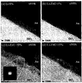
- HR-TEM 4 is a cross-sectional high resolution-transmission electron microscope (HR-TEM) image of a ZnO thin film doped with lithium hydroxide.
- SEM scanning electron microscope
- FIG. 6 to 10 are graphs showing electrical characteristics of a thin film transistor having a doped zinc oxide film.
- FIG. 6 is a undoped ZnO TFT as a comparative example
- FIG. 7 is a ZnO TFT doped with lithium
- FIG. 8 is a ZnO TFT doped with sodium
- FIG. 9 is a ZnO TFT doped with potassium
- FIG. 10 is rubidium ZnO doped with.
- (a) is an IV curve and (b) is a transition curve.
- 11 is a graph showing the electrical mobility by doping concentration when using lithium as a dopant.
- step S110 zinc oxide is reacted with zinc oxide to form a zinc amine complex.
- zinc amine complexes can be formed by dissolving 0.001 mole of zinc oxide in 12 ml of ammonia water and then cooling in a freezer for 5 hours. The use of a freezer is due to the nature of the zinc amine complex, which has increased solubility at low temperatures.
- Scheme 1 below a zinc amine complex is formed from crystalline zinc oxide (ZnO).
- step S120 the zinc amine complex and the hydroxide of an alkali metal or alkaline earth metal are mixed in a polar solvent to form a solution of zinc hydroxide.
- the hydroxide of the alkali metal may be lithium hydroxide (LiOH), sodium hydroxide (NaOH), potassium hydroxide (KOH), rubidium hydroxide (RbOH), cesium hydroxide (CsOH), the hydroxide of the alkaline earth metal is beryllium hydroxide (Be ( OH) 2 ), magnesium hydroxide (Mg (OH) 2 ), calcium hydroxide (Ca (OH) 2 ), strontium hydroxide (Sr (OH) 2 ), barium hydroxide (Ba (OH) 2 ).
- the alkali metal hydroxide may be lithium hydroxide (LiOH), sodium hydroxide (NaOH), potassium hydroxide (KOH), or rubidium hydroxide (RbOH).
- the alkali metal or alkaline earth metal may serve as a dopant for increasing the electro mobility of the zinc oxide film to be produced later.
- the hydroxides can be added to a solution in which a zinc amine complex is formed, for example, by making a solution of 0.1 to 1.5 M, taking 0.1 ml with a micropipette.
- Examples of the polar solvent are not particularly limited as long as the zinc amine complex and the hydroxide of the alkali metal are well dissolved, and include water and alcohols such as methanol and ethanol.
- Zinc hydroxide may be produced as shown in Scheme 2 below by the above-described method.
- n 1 to 4, and when the pH of the solution is increased, n may be close to 4. Since the pH of the ammonia water is high as 11.4, the zinc hydroxide may have the form of Zn (OH) 4 2- .
- the solution is applied onto a substrate to form a semiconductor film.
- the substrate may be a variety of substrates, for example, a semiconductor substrate (for example, silicon substrate), a glass substrate, a plastic substrate or a circuit board (for example a printed circuit board (PCB)).
- Various coating methods such as spin coating, spray coating and dip coating may be used for the application of the solution.
- an n-type zinc oxide film may be manufactured by heating the semiconductor film to form a zinc oxide film doped with the alkali metal or the alkaline earth metal.
- the semiconductor film may be heated to 200 to 500 ° C.
- the substrate is a plastic, it is preferable to heat to 300 ° C or less. Since the raw material used for the semiconductor film does not have a carbon chain component, high temperature is not required for sintering.
- the zinc hydroxide may be converted to zinc oxide as shown in Scheme 3 below.
- the zinc oxide film By the sintering, the zinc oxide film can be transformed into an amorphous zinc oxide film.
- the amorphous zinc oxide film produced by the above-described solution process may form a conduction band due to the overlapping phenomenon between ns orbitals of adjacent metals of ZnO, resulting in high mobility.
- the concentration of the alkali metal or alkaline earth metal in the doped zinc oxide film may be 0.001 to 20 mol%. Preferably the concentration may be 1 to 15 mol%. In the case of lithium doping, the effect of the electrical mobility is less when the concentration is less than 1 mol%, has a maximum value near 10 mol%, and when the concentration exceeds 15 mol%, the effect of increasing the electrical mobility may be reduced. In the case of sodium, potassium and rubidium, the concentration is preferably at a maximum value of 1 to 3 mol%, and when exceeding this value, the electric mobility decreases but is higher than that without dope.
- Doping with alkali or alkaline earth metals can act as a shallow donor.
- lithium (Li), sodium (Na), potassium (K), etc. may be substituted for zinc (Zn) sites or at interstitial sites.
- Zn zinc
- crevice doping can be located around oxygen vacancies to prevent lattice deformation of oxygen vacancies.
- Oxygen vacancies are known to increase carrier concentration and increase the electrical mobility of n-type semiconductors.
- the alkali metal or alkaline earth metal can be doped into the zinc oxide film in a chemically stable manner.
- the use of a solution process enables the formation of a semiconductor film having a high electrical mobility even at a low temperature process, and thus is applicable to a flexible substrate such as plastic. Therefore, a transparent and flexible display device can be manufactured.
- a zinc oxide thin film transistor including a semiconductor channel connecting between a source electrode and a drain electrode on a flexible substrate, wherein the semiconductor channel is an n-type zinc oxide film doped with an alkali metal or an alkaline earth metal
- the flexible substrate may be a plastic substrate. Examples of the plastic include PET, PEN, PC, PI, and the like.
- the semiconductor channel may be formed by a solution process using a zinc precursor free from carbon.
- a zinc precursor includes a carbon component such as zinc acetate
- a high sintering temperature above 300 ° C. is required.
- the zinc oxide thin film transistor has an on / off ratio of 10 6 or more, even when fabricated by low temperature sintering of 300 ° C. or less, which can be tolerated by a plastic substrate.
- the degree may be at least 5 cm 2 / Vs.
- the solution process may be performed by applying a solution containing a mixture of an alkali metal or alkaline earth metal hydroxide and a zinc amine complex on a substrate.
- a thin film transistor By using the n-type zinc oxide film described above as a driving unit of the display, a thin film transistor (TFT) can be manufactured.
- TFT thin film transistor
- FIG. 2 illustrates a zinc oxide thin film transistor (TFT) according to an embodiment of the disclosed technology.
- TFT zinc oxide thin film transistor
- a gate electrode 210 and a gate insulating layer 220 are formed on a substrate 200, and a semiconductor channel 230 and a channel protection layer 235 are formed thereon.
- the source / drain electrodes 240a and 240b may be formed at both sides of the semiconductor channel 230.
- the semiconductor channel 230 may be an amorphous n-type zinc oxide film doped with an alkali metal or an alkaline earth metal. Since the n-type zinc oxide film doped with alkali metal or alkaline earth metal may be manufactured by low temperature sintering, a silicon substrate as well as a flexible substrate such as plastic may be used as the substrate 200. Since the zinc oxide thin film transistor can be manufactured at low temperature, it is possible to increase the applicability of transparent and stable devices including medical and automotive head up display (HUD) products as well as LCD and OLED driving devices.
- HUD head up display
- step S310 a solution containing a mixture of an alkali metal or alkaline earth metal hydroxide and a zinc amine complex is applied onto a substrate to form a semiconductor film.
- step S320 the semiconductor film is sintered to form an amorphous n-type zinc oxide film.
- step S330 by forming the channel by patterning the amorphous n-type zinc oxide film, a zinc oxide thin film transistor having an n-type zinc oxide film as a semiconductor channel may be manufactured.
- the solution preferably contains a polar solvent so that both the alkali metal or alkaline earth metal hydroxide and the zinc amine complex can be dissolved well.
- the metal can be doped in such a manner that the metal is located in the gap of zinc, for example, to realize a device having a very high electric mobility.
- aqueous solution in which a zinc amine complex was formed was prepared by dissolving 0.001 mol of zinc oxide in 12 ml of ammonia water and then cooling it in a freezer for 5 hours to increase solubility.
- an aqueous solution for doping was prepared at concentrations of 0.1 M, 0.3 M, 0.5 M, 1 M, and 1.5 M for lithium hydroxide (LiOH), sodium hydroxide (NaOH), potassium hydroxide (KOH), and rubidium hydroxide (RbOH). .
- the doping aqueous solution was added to the aqueous solution in which the zinc amine complex was formed by taking 0.1 ml each using a micro pipette to prepare a solution for spin coating of a ZnO film.
- a thin film transistor of a bottom gate / top contact type was manufactured using the above-described solution for forming a ZnO film.
- a silicon wafer (SiO 2 (200 nm) / Si) including an insulating layer was used as the substrate.
- the concentration of alkali metal added to the ZnO solution for doping was 1-15 mol%, and the substrate was sintered at 300 ° C. on a hot plate for one hour so that the alkali metal was placed in the niche.
- FIG. 4 is a cross-sectional high resolution-transmission electron microscope (HR-TEM) image of a ZnO thin film doped with lithium hydroxide.
- HR-TEM high resolution-transmission electron microscope
- FIG. 4C looking at the fast fourier transform selective area electron diffraction (FFT-SAED) pattern of FIG. 4C, it can be seen that a dot pattern due to the lattice structure is formed. Circular faint bleeding of the FFT-SAED pattern is due to the amorphous structure of SiO 2 . As the doping concentration increased from 0 to 15 mol%, no unusual lattice distortion or migration was found.
- FFT-SAED fast fourier transform selective area electron diffraction
- FIG. 5 is a scanning electron microscope (SEM) photograph showing an amorphous zinc oxide film formed on a substrate. Referring to FIG. 5, it can be seen from the SEM photograph that an amorphous film having a thickness of about 100 nm is formed.
- the thin film transistor is a device in which conduction current flowing between the source and the drain is controlled by the gate voltage V G.
- V G gate voltage
- V G gate voltage
- excess electrons are attracted to the dielectric and semiconductor interface, forming a very thin accumulation layer at the semiconductor interface.
- the drain current I D in the saturated state can be represented by the following equation.
- I D Drain current
- W channel width
- L channel length
- ⁇ electrical mobility
- C i Capacitance of the dielectric
- V G Gate voltage
- the electrical properties of the prepared TFT were analyzed.
- FIG. 6 to 10 are graphs showing electrical characteristics of a thin film transistor having a doped zinc oxide film.
- FIG. 6 is a undoped ZnO TFT as a comparative example
- FIG. 7 is a ZnO TFT doped with lithium
- FIG. 8 is a ZnO TFT doped with sodium
- FIG. 9 is a ZnO TFT doped with potassium
- FIG. 10 is rubidium ZnO doped with.
- (a) is an IV curve and (b) is a transition curve.
- the transition curve was measured by fixing the drain current at 60V and sweeping the gate voltage from -60V to 60V.
- the value of the dynamic range expressed as the ratio of the on state current (I on ) to the off state current (I off ), that is, the on / off ratio must be large.
- FET field effect transistor
- the drain current hardly flows.
- the TFT since a semiconductor and an electrode make ohmic contact, a leakage current may flow in parallel with a channel through the semiconductor. If this leakage current becomes large, the drain current does not become saturated, and the off current cannot be reduced, and thus it loses its function as a switch element.
- the organic light emitting diode to become (OLED) using the driving device of the high-resolution display to the light emitting element is to be off-state current is less than 10 -9, and ON / OFF ratio of 10 6 or more, the electrical mobility of 5 cm 2 / Requires Vs.
- the IV output characteristics of the undoped ZnO TFT show that the saturation current value is well separated according to V G and the saturation state is well reached but the current value is not high.
- the graph in (b) shows that the off-state current is ⁇ 10A and the on / off ratio is about 104, which is not suitable for high quality display.
- the graph of (b) can be divided into linear and saturation regions, and the electrical mobility can be calculated from the above equation in the saturation region. As a result, the electrical mobility of the undoped ZnO TFT was considerably low, about 0.75 cm 2 / Vs.
- V G is the current starts flowing over from the 16V, and on-state current (on current) when the 40V work has shown a value higher by 0.00238A.
- the transition graph shows a high on / off ratio ( ⁇ 10), high electrical mobility (7.3414 cm2 / Vs) and low threshold voltage (7.7571V).
- the on-state current when V G is 40 V is 0.00297 A.
- the transition graph shows a high on / off ratio ( ⁇ 10), high electrical mobility (5.8501 cm2 / Vs) and low threshold voltage (5.9974 V).
- the transition graph shows a high on / off ratio ( ⁇ 10) compared to undoped, high electrical mobility of 3.6708 cm2 / Vs and threshold voltage of 0.9998V.
- the IV output characteristics show that current starts to flow when V G is 8V, and the current value when it is 40V is 0.00196A.
- the transition graph shows a high on / off ratio ( ⁇ 10) compared to undoped, high electrical mobility of 4.2682 cm2 / Vs and threshold voltage of 6.9904V.
- the following table compares the electrical characteristics of the TFTs according to the types of zinc oxide films.
- the concentration in parentheses of each zinc oxide on the left means the doping concentration.
- each lithium and sodium dopant was doped by 1, 3, 5, 10, 15mol%, respectively, and measured by configuring a TFT.
- FIGS. 11 and 12 are graph showing the electrical mobility by doping concentration when using lithium as a dopant
- Figure 12 is a graph showing the electrical mobility by doping concentration when using sodium as a dopant.
- a description of the box chart of FIGS. 11 and 12 is as follows.
Landscapes
- Thin Film Transistor (AREA)
Abstract
산화아연에 암모니아를 반응시켜 아연 아민 착체를 형성하는 단계; 상기 아연 아민 착체와 알칼리 금속 또는 알칼리 토금속의 수산화물을 극성 용매 중에서 혼합시켜 아연 수산화물의 용액을 형성하는 단계; 상기 용액을 기판 상에 도포하여 반도체 막을 형성하는 단계; 및 상기 반도체 막을 가열하여 상기 알칼리 금속 또는 상기 알칼리 토금속으로 도핑된 산화아연 막을 형성하는 단계를 포함하는 n형 산화아연 막의 제조방법이 제공된다.
Description
본 명세서에 개시된 기술은 산화아연 박막 트랜지스터 및 이의 제조방법에 관한 것으로 보다 상세하게는 전기적 특성이 우수하면서도 제조시 공정이 간단하고 경제적인 산화아연 박막 트랜지스터 및 이의 제조방법에 관한 것이다.
차세대 디스플레이 기술에 있어서 높은 해상도, 광학적 투명도, 기계적 유연성을 가지는 것이 매우 중요하다. 이때 디스플레이를 구성하는 구동부와 발광부는 이에 따른 적당한 성질을 가져야한다. 적합한 성질을 가지는 구동부로서의 트랜지스터와 집적 회로를 설계하는 것이 날로 중요해지고 있다.
현재 a-Si:H와 p-Si 박막 트랜지스터는 AMLCD와 AMOLED의 구동부로 널리 쓰이고 있다. 하지만 이러한 물질들은 몇 가지 제한요소가 있는데 a-Si:H의 경우 고해상도 디스플레이에 필요한 전기 이동도가 부족하거나(~1 cm²/Vs), 높은 제작단가, 및 진공 증착이나 높은 온도 등의 가혹한 조건이 필요한 문제가 있다. 이 뿐만 아니라 실리콘을 기반으로 하는 반도체는 낮은 인장 변형률(tensile strain) 특성을 가지고 있어서 유연성을 가지는 디스플레이에는 적용하기가 어렵다. 이러한 문제점을 해결하기 위해서 금속 산화물이 대체물로 부각되기 시작했다. 금속 산화물은 그 물질의 성격에 따라 전도체, 반도체, 부도체등으로 각각 사용된다. 특히 그 중 산화아연(Zinc Oxide)은 우수한 반도체 물질로 3.3eV의 높은 밴드갭을 가지고 있어 광학적 투명도가 매우 좋으며, 화학적 안정성과 높은 전기 이동도를 가지고 있다. 순수한 ZnO의 전기 이동도는 고화질의 디스플레이에는 부족하기 때문에 대부분이 도핑을 하여 사용하고 있으며 인듐 아연 산화물(IZO), 인듐 갈륨 아연 산화물(IGZO), 인듐 주석 산화물(ZTO) 등이 대표적인 예이다. 하지만 높은 이동도를 확보해주는 인듐은 희토류 금속으로서 높은 가격적 문제와 소결온도가 400 ~ 500℃가 되어야 하여 사용되는 기판에 제한이 있다.
ZnO TFT를 구성하기 위해서 ZnO 박막을 구성하는 방법에는 라디오 주파수(RF) 마그네트론 스퍼터링, 화학 기상 증착(CVD), 스프레이 파이롤리시스(spray pyrolysis) 등이 있다. 대개의 경우 진공장비를 사용하여 대면적 코팅이 어렵고 비용이 높으므로 새로운 공정개발의 필요성이 대두된다.
본 개시된 기술의 일 측면에 의하면, 산화아연에 암모니아를 반응시켜 아연 아민 착체를 형성하는 단계; 상기 아연 아민 착체와 알칼리 금속 또는 알칼리 토금속의 수산화물을 극성 용매 중에서 혼합시켜 아연 수산화물의 용액을 형성하는 단계; 상기 용액을 기판 상에 도포하여 반도체 막을 형성하는 단계; 및 상기 반도체 막을 가열하여 상기 알칼리 금속 또는 상기 알칼리 토금속으로 도핑된 산화아연 막을 형성하는 단계를 포함하는 n형 산화아연 막의 제조방법이 제공된다.
본 개시된 기술의 다른 측면에 의하면, 플렉시블 기판 상에 소스 전극과 드레인 전극 사이를 연결하는 반도체 채널을 포함하되, 상기 반도체 채널은 알칼리 금속 또는 알칼리 토금속으로 도핑된 n형 산화아연 막인 산화아연 박막 트랜지스터가 제공된다.
본 개시된 기술의 또 다른 측면에 의하면, 알칼리 금속 또는 알칼리 토금속의 수산화물과 아연 아민 착체의 혼합물을 함유한 용액을 기판 상에 도포하여 반도체 막을 형성하는 단계; 상기 반도체 막을 소결하여 n형 산화아연 막을 형성하는 단계; 및 상기 n형 산화아연 막을 패터닝하여 반도체 채널을 형성하는 단계를 포함하는 산화아연 박막 트랜지스터의 제조방법이 제공된다.
본 개시된 기술의 또 다른 측면에 의하면, 산화아연에 암모니아를 반응시켜 아연 아민 착체를 형성하는 단계; 상기 아연 아민 착체와 알칼리 금속의 수산화물을 극성 용매 중에서 혼합시켜 아연 수산화물의 용액을 형성하는 단계; 상기 용액을 플라스틱 기판 상에 도포하여 반도체 막을 형성하는 단계; 및 상기 반도체 막을 300℃ 이하로 가열하여 상기 알칼리 금속으로 도핑된 산화아연 막을 형성하는 단계를 포함하는 산화아연 박막 트랜지스터의 제조방법이 제공된다.
도 1은 개시된 기술의 일 실시예에 따른 n형 산화아연 막의 제조방법을 나타내는 공정흐름도이다.
도 2는 개시된 기술의 일 실시예에 따른 산화아연 박막 트랜지스터(TFT)를 나타내는 도면이다.
도 3은 개시된 기술의 일 실시예에 따른 산화아연 박막 트랜지스터(TFT)의 제조방법을 나타내는 공정흐름도이다.
도 4는 수산화 리튬으로 도핑된 ZnO 박막의 단면 HR-TEM(high resolution-transmission electron microscope) 이미지이다.
도 5는 기판 상에 형성된 비정질 산화아연 필름을 나타낸 주사전자현미경(SEM) 사진이다.
도 6 내지 도 10은 도핑된 산화아연 막을 구비한 박막 트랜지스터의 전기적 특성을 나타낸 그래프이다. 도 6은 비교예로서 도핑되지 않은 ZnO TFT이고, 도 7은 리튬으로 도핑된 ZnO TFT이고, 도 8은 나트륨으로 도핑된 ZnO TFT이고, 도 9는 칼륨으로 도핑된 ZnO TFT이고, 도 10은 루비듐으로 도핑된 ZnO TFT를 나타낸다. 각 도면에서 (a)는 IV 곡선 이고 (b)는 전이곡선을 나타낸다.
도 11은 리튬을 도펀트로 사용하였을 때의 도핑 농도별 전기 이동도를 나타낸 그래프이다.
도 12는 나트륨을 도펀트로 사용하였을 때의 도핑 농도별 전기 이동도를 나타낸 그래프이다.
이하, 도면을 참조하여 본 개시된 기술의 실시예들에 대해 상세히 설명하고자 한다. 다음에 소개되는 실시예들은 당업자에게 개시된 사상이 충분히 전달될 수 있도록 하기 위해 예로서 제공되어지는 것이다. 따라서 본 개시된 기술은 이하 설명된 실시예들에 한정되지 않고 다른 형태로 구체화될 수도 있다. 그리고 도면들에 있어서, 구성요소의 폭, 길이, 두께 등은 편의를 위하여 과장되어 표현될 수도 있다. 명세서 전체에 걸쳐서 동일한 참조번호들은 동일한 구성요소들을 나타낸다. 전체적으로 도면 설명시 관찰자 시점에서 설명하였고, 층, 막 등의 부분이 다른 부분 위에있다고 할 때, 이는 다른 부분 바로 위에있는 경우 뿐 아니라, 그 중간에 또 다른 부분이 있는 경우도 포함한다.
도 1은 개시된 기술의 일 실시예에 따른 n형 산화아연 막의 제조방법을 나타내는 공정흐름도이다. 도 1을 참조하면, 단계 S110에서, 산화아연에 암모니아를 반응시켜 아연 아민 착체를 형성한다. 예를 들어 산화아연 0.001 몰을 암모니아수 12 ml에 녹인 다음 냉동고에서 5시간 동안 냉각시키는 방법으로 아연 아민 착체를 형성할 수 있다. 냉동고를 사용하는 것은 저온에서 용해도가 증가하는 아연 아민 착체의 성질에 기인한다. 아래 반응식 1에 결정성 산화아연(ZnO)으로부터 아연 아민 착체가 형성되는 과정을 나타내었다.
(반응식 1) ZnO(c) + 4NH3(aq) + 2H+(aq) → Zn(NH3)4
2+(aq) + H2O(l)
단계 S120에서, 상기 아연 아민 착체와 알칼리 금속 또는 알칼리 토금속의 수산화물을 극성 용매 중에서 혼합시켜 아연 수산화물의 용액을 형성한다.
상기 알칼리 금속의 수산화물은 수산화리튬(LiOH), 수산화나트륨(NaOH), 수산화칼륨(KOH), 수산화루비듐(RbOH), 수산화세슘(CsOH)일 수 있으며, 상기 알칼리 토금속의 수산화물은 수산화베릴륨(Be(OH)2), 수산화마그네슘(Mg(OH)2), 수산화칼슘(Ca(OH)2), 수산화스트론튬(Sr(OH)2), 수산화바륨(Ba(OH)2)일 수 있다. 바람직하게는 상기 알칼리 금속의 수산화물은 수산화리튬(LiOH), 수산화나트륨(NaOH), 수산화칼륨(KOH), 수산화루비듐(RbOH)일 수 있다. 상기 알칼리 금속 또는 알칼리 토금속은 이후 생성되는 산화아연 막의 전기이동도를 증가시키기 위한 도펀트로 작용할 수 있다. 상기 수산화물들은 예를 들어 0.1 내지 1.5M의 용액을 만들어 마이크로 피펫으로 0.1ml를 취하여 아연 아민 착체가 형성된 용액에 첨가될 수 있다.
상기 극성 용매의 예는 상기 아연 아민 착체와 상기 알칼리 금속의 수산화물이 잘 용해되는 용매라면 특별히 제한되지 않으며, 물 및 메탄올, 에탄올 등의 알코올류를 포함한다.
아연 수산화물은 상술한 방법으로 아래의 반응식 2와 같이 생성될 수 있다.
(반응식 2) Zn(NH3)4
2+ + n OH- → [Zn(NH3)4-n(OH)n]2-n + n NH3
여기서 n은 1 내지 4이고, 용액의 pH가 높아지면 n은 4에 가까워질 수 있다. 암모니아수의 pH가 11.4로 높은 상태이기 때문에 상기 아연 수산화물은 Zn(OH)4
2-의 형태를 가질 수 있다.
단계 S130에서, 상기 용액을 기판 상에 도포하여 반도체 막을 형성한다. 상기 기판은 다양한 종류의 기판이 사용될 수 있으며, 예로 반도체 기판(일례: 실리콘 기판), 유리 기판, 플라스틱 기판 또는 회로 기판(일례 PCB(printed circuit board))일 수 있다. 상기 용액의 도포를 위해 스핀코팅, 분무코팅, 딥코팅 등 다양한 공지의 방식을 사용할 수 있다.
단계 S140에서, 상기 반도체 막을 가열하여 상기 알칼리 금속 또는 상기 알칼리 토금속으로 도핑된 산화아연 막을 형성함으로써 n형 산화아연 막이 제조될 수 있다. 상기 반도체 막은 200 내지 500℃로 가열할 수 있다. 상기 기판이 플라스틱인 경우 300℃ 이하로 가열하는 것이 바람직하다. 상기 반도체 막에 사용되는 원료에는 탄소 사슬 성분이 없으므로 소결 시 높은 온도가 필요하지 않다.
상기 가열에 의해 아연 수산화물은 아래의 반응식 3과 같이 산화아연으로 변환될 수 있다.
(반응식 3) Zn(OH)4
2- → ZnO + H2O + 2OH-
상기 소결에 의해 상기 산화아연 막은 비정질(amorphous) 산화아연 막으로 변할 수 있다. 상술한 용액공정으로 생성된 비정질 산화아연 막은 ZnO의 근접한 금속의 ns 오비탈 간의 겹침 현상으로 인해서 전도띠를 형성하여 높은 이동도를 가져올 수 있다. 상기 도핑된 산화아연 막 내의 상기 알칼리 금속 또는 상기 알칼리 토금속의 농도는 0.001 내지 20 mol%일 수 있다. 바람직하게는 상기 농도는 1 내지 15 mol%일 수 있다. 리튬 도핑의 경우에는 상기 농도가 1 mol% 미만에서는 전기 이동도의 효과가 적고, 10 mol% 근처에서 최대값을 가지며, 15 mol%를 초과하면 전기 이동도의 증가 효과가 감소할 수 있다. 나트륨, 칼륨, 루비듐의 경우에는 농도가 바람직하게는 1 내지 3 mol%에서 최대값을 보이며 이 값을 초과하는 경우에는 전기 이동도가 감소하지만 도핑을 하지 않은 경우보다는 높다.
알칼리 금속 또는 알칼리 토금속이 도핑되면 얕은 공여체(shallow donor) 역할을 할 수 있다. 알칼리 금속 또는 알칼리 토금속을 도핑할 때에는 두 가지 방식이 존재할 수 있다. 예를 들어, 알칼리 금속이 도핑될 때, 리튬(Li), 나트륨(Na), 칼륨(K) 등이 아연(Zn) 자리를 치환(substitutianal site)하거나 틈새 자리(interstitial site)에 위치하는 방식일 수 있다. 실제에 있어서, 알칼리 금속이 산화아연에 도핑될 때 치환 방식보다는 틈새 자리에 위치하는 방식으로 도핑되는 것이 선호되는 것으로 알려져 있다. 이 경우, 틈새 자리의 알칼리 금속은 주개(donor) 불순물의 역할을 하기 때문에 n형 반도체의 성질을 강화할 수 있다.
또한 틈새 자리 도핑은 산소 빈자리(oxygen vacancy) 주변에 위치하여 산소 빈자리의 격자 변형을 방지할 수 있다. 산소 빈자리는 캐리어 농도의 증가와 n형 반도체의 전기 이동도를 높여주는 것으로 알려져 있다.
상술한 제조방법에 따르면, 화학적으로 안정한 방식으로 알칼리 금속 또는 알칼리 토금속을 산화아연 막에 도핑할 수 있다. 또한 용액 공정을 사용함으로써 저온 공정에서도 높은 전기 이동도를 갖는 반도체 막의 형성이 가능하므로 플라스틱과 같은 플렉시블 기판에도 적용가능하다. 따라서 투명하고 유연한 디스플레이 소자를 제조할 수 있다.
일 실시예에 따르면, 플렉시블 기판 상에 소스 전극과 드레인 전극 사이를 연결하는 반도체 채널을 포함하되, 상기 반도체 채널은 알칼리 금속 또는 알칼리 토금속으로 도핑된 n형 산화아연 막인 산화아연 박막 트랜지스터가 제공될 수 있다. 상기 플렉시블 기판은 플라스틱 기판일 수 있다. 상기 플라스틱의 예로 PET, PEN, PC, PI 등을 들 수 있다.
상기 반도체 채널은 탄소 성분이 없는 아연 전구체를 사용한 용액 공정에 의해 형성될 수 있다. 예를 들어, 아연 전구체로 아연 아세테이트와 같은 탄소 성분이 포함될 경우 300℃를 넘는 높은 소결 온도가 필요하다. 반면, 탄소 성분이 없는 아연 전구체를 사용하여 용액 공정으로 제조될 경우, 플라스틱 기판이 견딜 수 있는 300℃ 이하의 저온 소결로 제작하여도 산화아연 박막 트랜지스터는 온/오프 비가 106 이상이고, 전기 이동도가 5 cm2/Vs 이상일 수 있다. 예를 들어, 상기 용액 공정은 알칼리 금속 또는 알칼리 토금속의 수산화물과 아연 아민 착체의 혼합물을 함유한 용액을 기판 상에 도포하여 수행될 수 있다.
상술한 n형 산화아연 막을 디스플레이의 구동부로 이용함으로써, 박막 트랜지스터(TFT)를 제조할 수 있다.
도 2는 개시된 기술의 일 실시예에 따른 산화아연 박막 트랜지스터(TFT)를 나타내는 도면이다. 도 2를 참조하면, 산화아연 박막 트랜지스터는 기판(200) 상에 게이트 전극(210), 게이트 절연막(220)이 형성되고, 그 위에 반도체 채널(230) 및 채널 보호층(235)이 형성되어 있으며, 반도체 채널(230)의 양 옆으로 소스/드레인 전극(240a, 240b)이 형성될 수 있다.
반도체 채널(230)은 알칼리 금속 또는 알칼리 토금속으로 도핑된 비정질 n형 산화아연 막일 수 있다. 알칼리 금속 또는 알칼리 토금속으로 도핑된 n형 산화아연 막은 저온 소결방식으로 제조될 수 있으므로, 기판(200)으로서 실리콘 기판은 물론, 플라스틱과 같은 플렉시블 기판도 사용될 수 있다. 상기 산화아연 박막 트랜지스터는 저온 제작이 가능하므로 기존이 LCD, OLED 구동소자뿐만 아니라 의료용 및 자동차 HUD(head up display) 제품을 포함한 투명하고 안정한 소자의 응용가능성을 높일 수 있다.
도 3은 개시된 기술의 일 실시예에 따른 산화아연 박막 트랜지스터(TFT)의 제조방법을 나타내는 공정흐름도이다. 도 3을 참조하면, 단계 S310에서, 알칼리 금속 또는 알칼리 토금속 수산화물과 아연 아민 착체의 혼합물을 함유한 용액을 기판 상에 도포하여 반도체 막을 형성한다. 단계 S320에서, 상기 반도체 막을 소결하여 비정질 n형 산화아연 막을 형성한다. 단계 S330에서, 상기 비정질 n형 산화아연 막을 패터닝하여 채널을 형성함으로써, n형 산화아연 막을 반도체 채널로 구비한 산화아연 박막 트랜지스터가 제조될 수 있다.
상기 용액은 상기 알칼리 금속 또는 알칼리 토금속 수산화물과 아연 아민 착체 모두 잘 녹을 수 있도록 극성 용매를 포함하는 것이 바람직하다. 이와 같은 용액 공정을 활용하면, 금속이 예를 들어 아연의 틈새 자리에 위치하도록 하는 방식으로 금속의 도핑이 될 수 있어서 전기 이동도가 매우 높은 소자를 구현할 수 있다. 상술한 방법을 사용할 경우 고화질의 유연성을 가지는 디스플레이를 구현하기 위해서 가져야하는 낮은 제작 온도, 높은 전기 이동도, 화학적 안정성을 확보할 수 있으므로 고화질의 유연성을 가지는 디스플레이를 구현할 수 있다.
이하, 구체적인 실시예를 들어 본 개시된 기술에 대해 보다 상세히 설명하고자 한다.
(실시예)
도핑된
산화아연 막 형성을 위한 용액 제조
0.001 mol의 산화아연(zinc oxide)를 12 ml의 암모니아수에 녹인 다음 냉동고에서 5시간 동안 용해도를 증가시키기 위하여 냉각시킴으로써 아연 아민 착체(zinc amine complex)가 형성된 수용액을 제조하였다. 다음 도핑을 위해 수산화리튬(LiOH), 수산화나트륨(NaOH), 수산화칼륨(KOH), 수산화루비듐(RbOH)에 대해 0.1M, 0.3M, 0.5M, 1M, 1.5M의 농도별로 도핑용 수용액을 만들었다. 상기 도핑용 수용액을 마이크로 피펫을 이용하여 0.1 ml씩 취하여 상기 아연 아민 착체가 형성된 수용액에 첨가하여 이후 ZnO 막의 스핀 코팅을 위한 용액을 제조하였다.
산화아연 박막 트랜지스터 제조
상술한 ZnO 막 형성용 용액을 사용하여 보텀 게이트/탑 콘택트(bottom gate/top contact) 방식의 박막 트랜지스터를 제작하였다. 기판으로서 절연층을 포함하는 실리콘 웨이퍼(SiO2 (200 nm)/Si)를 기판으로 사용하였다. 상기 기판 상에 ZnO 막 형성용 용액을 3000 rpm에서 30초간 스핀 코팅하여 반도체 막을 형성하였다. 다음 쉐도우 마스크를 사용하여 80 nm 두께의 알루미늄을 열증착하여 소스 및 드레인 전극들(W/L=20)을 형성하였다. 도핑을 위해 ZnO 용액에 첨가된 알칼리 금속의 농도는 1~ 15 mol%였으며, 알칼리 금속이 틈새 자리에 위치하도록 상기 기판을 핫 플레이트 상에서 300℃로 한 시간 동안 소결하였다.
산화아연 박막 트랜지스터 특성 평가
도 4는 수산화 리튬으로 도핑된 ZnO 박막의 단면 HR-TEM(high resolution-transmission electron microscope) 이미지이다. 도 4를 참조하면, ZnO 박막의 격자 구조를 확인할 수 있으며 이를 통하여 다결정질 구조(polycrystalline sturcture)가 잘 형성되었음을 알 수 있다. 또한 도 4 (c) 의 FFT-SAED (fast fourier transform selective area electron diffraction) 패턴을 보면, 격자 구조로 인한 도트 패턴(dot pattern)이 형성되는 것을 알 수 있다. FFT-SAED 패턴의 원형의 희미한 번짐은 SiO2의 비정질(amorphous) 구조로 인해 형성된 것이다. 도핑농도가 0~15 mol% 까지 증가함에 특이한 격자 비틀림(lattice distortion)이나 마이그레이션(migration)은 발견되지 않았다.
도 5는 기판 상에 형성된 비정질 산화아연 필름을 나타낸 주사전자현미경(SEM) 사진이다. 도 5를 참조하면, SEM 사진으로부터 비정질의 약 100nm 두께의 필름이 형성되었음을 알수 있다.
박막 트랜지스터는 소스-드레인 사이를 흐르는 전도전류가 게이트 전압(VG)에 의해 조절되는 소자이다. 소스를 공통 접지로 하여 게이트 전극에 양의 전압을 인가하게 되면 과잉 전자들이 유전체와 반도체 계면으로 이끌려 반도체 계면에는 매우 얇은 축적층을 형성한다. 여기서 포화상태에서의 드레인 전류 ID는 이하의 식으로 나타낼 수 있다.
식: 
ID
= 드레인 전류, W = 채널의 폭, L = 채널의 길이, μ = 전기 이동도(mobility), Ci
= 유전체의 커패시턴스, VG
= 게이트 전압, VT
= 문턱 전압
여기서,  (K : 유전상수(Dielectric constant), ε0 : 진공 유전율, A : 유전체의 면적, t : 유전체의 두께)
상기 제조된 TFT의 전기적 특성을 분석하였다.
도 6 내지 도 10은 도핑된 산화아연 막을 구비한 박막 트랜지스터의 전기적 특성을 나타낸 그래프이다. 도 6은 비교예로서 도핑되지 않은 ZnO TFT이고, 도 7은 리튬으로 도핑된 ZnO TFT이고, 도 8은 나트륨으로 도핑된 ZnO TFT이고, 도 9는 칼륨으로 도핑된 ZnO TFT이고, 도 10은 루비듐으로 도핑된 ZnO TFT를 나타낸다. 각 도면에서 (a)는 IV 곡선 이고 (b)는 전이곡선을 나타낸다.
전이 곡선은 드레인 전류를 60V로 고정하고 게이트 전압을 -60V에서부터 60V까지 스윕하여 측정을 하였다. TFT가 좋은 스위치 기능을 가지려면 온 상태 전류 (Ion)과 오프 상태 전류(Ioff)의 비, 즉 온/오프 비로 표현되는 동적 영역의 값이 커야 한다. 전계효과 트랜지스터(FET)의 경우에는 게이트 전압이 0이면 드레인 전류는 거의 흐르지 않는다. 반면에 박막 트랜지스터(TFT)는 반도체와 전극이 오믹 접촉(ohmic contact)을 이루고 있으므로 반도체를 통해 채널과 평행으로 누설전류가 흐를 수 있다. 만일 이러한 누설전류가 커지게 되면 드레인 전류는 포화가 되지 않을 뿐만 아니라 오프 상태 전류(off current)를 줄일 수 없어 스위치 소자로서 기능을 상실한다. 일반적으로 유기발광다이오드(OLED)를 발광소자로하는 고화질 디스플레이의 구동소자로 사용되기 위해서는 오프 상태 전류가 10-9 이하가 되어야 하며 온/오프 비는 106 이상, 전기 이동도는 5 cm2/Vs를 요구한다.
도 6을 참조하면, (a)로부터, 도핑하지 않은 ZnO TFT의 IV 출력 특성을 보면 VG에 따라 포화전류 값이 잘 분리되며 포화상태에 잘 도달하지만 전류 값이 높지 않은 것을 알 수 있다. (b)의 그래프를 보게 되면 오프 상태 전류가 ~10A이며 온/오프 비가 10⁴정도로 고화질의 디스플레이에 사용하기에는 적합하지 않은 성능을 보여주고 있다. (b)의 그래프는 선형영역과 포화영역으로 나눌 수 있는데 포화영역에서 상기 식을 통하여 전기 이동도를 계산할 수 있다. 계산 결과, 도핑 되지 않은 ZnO TFT의 전기 이동도가 0.75 cm2/Vs정도로 상당히 낮았다.
도 7은 수산화리튬을 10 mol% 도핑한 TFT의 전기적 특성이다. IV 출력 특성을 보면 VG(0V~40V step=8V)에 따른 각각의 전류값이 잘 분리되고 포화된다. VG가 16V일 때부터 전류가 흐르기 시작하며, 40V일 때의 온 상태 전류(on current)는 0.00238A로 높은 값을 보여주고 있다. 전이 그래프를 보면 높은 온/오프 비(~10)를 확보하였으며, 높은 전기 이동도 (7.3414cm²/Vs) 와 낮은 문턱전압 (7.7571V)을 보여주고 있다.
도 8은 수산화나트륨을 1 mol% 도핑한 TFT의 전기적 특성이다. IV 출력 특성을 보면 VG(0V~40V step=8V)에 따른 각각의 전류값이 잘 분리되고 포화된다. VG가 40V일 때의 온 상태 전류는 0.00297A이다. 전이 그래프를 보면 높은 온/오프 비(~10)를 확보하였으며, 높은 전기 이동도 (5.8501cm²/Vs)와 낮은 문턱전압 (5.9974V)을 보여주고 있다.
도 9는 수산화칼륨을 3 mol% 도핑한 TFT의 전기적 특성을 보여준다. IV 출력 특성을 보면 VG가 8V일 때부터 전류가 흐르기 시작하며 40V일 때의 흐르는 전류값은 0.00223A 이다. 전이그래프를 보면 도핑하지 않은 것에 비해 높은 온/오프 비(~10)를 보여주며, 3.6708cm²/Vs의 높은 전기 이동도와 0.9998V의 문턱전압을 나타내고 있다.
도 10은 수산화루비듐을 1mol% 도핑한 TFT의 전기적 특성을 보여준다. IV 출력 특성을 보면 VG가 8V일 때부터 전류가 흐르기 시작하며 40V일 때의 흐르는 전류값은 0.00196A 이다. 전이그래프를 보면 도핑하지 않은 것에 비해 높은 온/오프 비(~10)를 보여주며, 4.2682cm²/Vs의 높은 전기 이동도와 6.9904V의 문턱전압을 나타내고 있다.
이하 표에 각 산화아연 막의 종류에 따른 TFT의 전기적 특성을 비교하여 나타내었다. 표 1에서 좌측의 각 산화아연의 괄호 안 농도는 도핑 농도를 의미한다.
표 1 산화아연 막 종류에 다른 TFT의 전기적 특성
| 전기이동도 (cm2/Vs) | 문턱 전압 (V) | 온/오프 비 | |
| ZnO | 1.5745 | 6.9170 | ~106 |
| Li-ZnO (10mol%) | 7.3414 | 7.7571 | ~107 |
| Na-ZnO (1mol%) | 5.8501 | 5.9974 | ~107 |
| K-ZnO (3mol%) | 3.6708 | 0.9998 | ~107 |
| Rb-ZnO (1mol%) | 4.2682 | 6.9904 | ~107 |
한편, 각 도펀트의 농도에 따른 성능 변화를 알아보기 위해 각 리튬과 나트륨 도펀트를 각각 1, 3, 5, 10, 15mol% 도핑한 후 TFT를 구성하여 측정하였다.
도 11은 리튬을 도펀트로 사용하였을 때의 도핑 농도별 전기 이동도를 나타낸 그래프이고, 도 12는 나트륨을 도펀트로 사용하였을 때의 도핑 농도별 전기 이동도를 나타낸 그래프이다. 도 11 및 12의 박스 차트에 대한 설명은 아래와 같다.
Maximum : 결과를 유도해낸 데이터 중의 최대값
Upper quartile : 전체 데이터 중 상위 75%에 해당하는 값
Average : 평균값
Median : 중간값
Lower quartile : 전제 데이터 중 하위 25%에 해당하는 값
Minimum : 결과를 유도해낸 데이터 중의 최대값
이상에서 본 개시된 기술의 실시예들에 대해 상세히 기술하였지만, 해당 기술분야에 있어서 통상의 지식을 가진 사람이라면, 본 개시된 기술의 정신 및 범위를 벗어나지 않으면서 본 실시예들을 여러 가지로 변형하여 실시할 수 있음을 이해할 수 있을 것이다.
Claims (13)
- 산화아연에 암모니아를 반응시켜 아연 아민 착체를 형성하는 단계;상기 아연 아민 착체와 알칼리 금속 또는 알칼리 토금속의 수산화물을 극성 용매 중에서 혼합시켜 아연 수산화물의 용액을 형성하는 단계;상기 용액을 기판 상에 도포하여 반도체 막을 형성하는 단계; 및상기 반도체 막을 가열하여 상기 알칼리 금속 또는 상기 알칼리 토금속으로 도핑된 산화아연 막을 형성하는 단계를 포함하는 n형 산화아연 막의 제조방법.
- 제1 항에 있어서,상기 도핑된 산화아연 막 내의 상기 알칼리 금속 또는 상기 알칼리 토금속의 농도가 0.001 내지 20 mol% 인 n형 산화아연 막의 제조방법.
- 제1 항 또는 제2 항에 있어서,상기 기판이 플라스틱인 n형 산화아연 막의 제조방법.
- 제3 항에 있어서,상기 가열 온도는 300℃ 이하인 n형 산화아연 막의 제조방법.
- 플렉시블 기판 상에 소스 전극과 드레인 전극 사이를 연결하는 반도체 채널을 포함하되,상기 반도체 채널은 알칼리 금속 또는 알칼리 토금속으로 도핑된 n형 산화아연 막인 산화아연 박막 트랜지스터.
- 제5 항에 있어서,상기 플렉시블 기판이 플라스틱 기판인 산화아연 박막 트랜지스터.
- 제5 항에 있어서,온/오프 비가 106 이상이고, 전기 이동도가 5 cm2/Vs 이상인 산화아연 박막 트랜지스터.
- 제5 항 내지 제7 항 중 어느 한 항에 있어서,상기 반도체 채널이 탄소 성분이 없는 아연 전구체를 사용한 용액 공정에 의해 형성된 산화아연 박막 트랜지스터.
- 제8 항에 있어서,상기 용액 공정은 알칼리 금속 또는 알칼리 토금속의 수산화물과 아연 아민 착체의 혼합물을 함유한 용액을 기판 상에 도포하여 수행되는 산화아연 박막 트랜지스터.
- 알칼리 금속 또는 알칼리 토금속의 수산화물과 아연 아민 착체의 혼합물을 함유한 용액을 기판 상에 도포하여 반도체 막을 형성하는 단계;상기 반도체 막을 소결하여 n형 산화아연 막을 형성하는 단계; 및상기 n형 산화아연 막을 패터닝하여 반도체 채널을 형성하는 단계를 포함하는 산화아연 박막 트랜지스터의 제조방법.
- 제10 항에 있어서,상기 도핑된 산화아연 막 내의 상기 알칼리 금속 또는 상기 알칼리 토금속의 농도가 1 내지 15 mol% 인 n형 산화아연 막의 제조방법.
- 산화아연에 암모니아를 반응시켜 아연 아민 착체를 형성하는 단계;상기 아연 아민 착체와 알칼리 금속의 수산화물을 극성 용매 중에서 혼합시켜 아연 수산화물의 용액을 형성하는 단계;상기 용액을 플라스틱 기판 상에 도포하여 반도체 막을 형성하는 단계; 및상기 반도체 막을 300℃ 이하로 가열하여 상기 알칼리 금속으로 도핑된 산화아연 막을 형성하는 단계를 포함하는 산화아연 박막 트랜지스터의 제조방법.
- 제12 항에 있어서,온/오프 비가 106 이상이고, 전기 이동도가 5 cm2/Vs 이상인 산화아연 박막 트랜지스터.
Applications Claiming Priority (2)
| Application Number | Priority Date | Filing Date | Title |
|---|---|---|---|
| KR1020110027226A KR101192221B1 (ko) | 2011-03-25 | 2011-03-25 | 산화아연 박막 트랜지스터 및 이의 제조방법 |
| KR10-2011-0027226 | 2011-03-25 |
Publications (2)
| Publication Number | Publication Date |
|---|---|
| WO2012134105A2 true WO2012134105A2 (ko) | 2012-10-04 |
| WO2012134105A3 WO2012134105A3 (ko) | 2013-01-03 |
Family
ID=46932072
Family Applications (1)
| Application Number | Title | Priority Date | Filing Date |
|---|---|---|---|
| PCT/KR2012/002088 Ceased WO2012134105A2 (ko) | 2011-03-25 | 2012-03-22 | 산화아연 박막 트랜지스터 및 이의 제조방법 |
Country Status (2)
| Country | Link |
|---|---|
| KR (1) | KR101192221B1 (ko) |
| WO (1) | WO2012134105A2 (ko) |
Family Cites Families (4)
| Publication number | Priority date | Publication date | Assignee | Title |
|---|---|---|---|---|
| TWI221341B (en) | 2003-09-18 | 2004-09-21 | Ind Tech Res Inst | Method and material for forming active layer of thin film transistor |
| JP4386747B2 (ja) * | 2004-01-28 | 2009-12-16 | 三洋電機株式会社 | p型ZnO半導体膜及びその製造方法 |
| US7851380B2 (en) * | 2007-09-26 | 2010-12-14 | Eastman Kodak Company | Process for atomic layer deposition |
| KR20100055655A (ko) * | 2008-11-18 | 2010-05-27 | 국민대학교산학협력단 | n-타입 ZnO 반도체 박막의 제조 방법 및 박막 트랜지스터 |
-
2011
- 2011-03-25 KR KR1020110027226A patent/KR101192221B1/ko not_active Expired - Fee Related
-
2012
- 2012-03-22 WO PCT/KR2012/002088 patent/WO2012134105A2/ko not_active Ceased
Also Published As
| Publication number | Publication date |
|---|---|
| KR20120108851A (ko) | 2012-10-05 |
| WO2012134105A3 (ko) | 2013-01-03 |
| KR101192221B1 (ko) | 2012-10-17 |
Similar Documents
| Publication | Publication Date | Title |
|---|---|---|
| RU2556102C2 (ru) | Оксид р-типа, получение оксидной композиции р-типа, способ получения оксида р-типа, полупроводниковый прибор, индикаторное устройство, аппаратура воспроизведения изображения и система | |
| US9673048B2 (en) | Method of producing thin film transistor, thin film transistor, display device, image sensor, and X-ray sensor | |
| CN101118860B (zh) | 使用水解制造氧化锌半导体 | |
| US8513646B2 (en) | Solution-processed high mobility inorganic thin-film transistors | |
| US9536957B2 (en) | P-type oxide, composition for producing p-type oxide, method for producing p-type oxide, semiconductor element, display element, image display device, and system | |
| US10032923B2 (en) | Metal oxide thin film, method for manufacturing the same, and solution for metal oxide thin film | |
| US20120003795A1 (en) | Manufacturing method of semiconductor device | |
| TW201724284A (zh) | 顯示裝置及包含該裝置之電子裝置 | |
| WO2010110571A2 (en) | Oxide semiconductor and thin film transistor including the same | |
| JP2017126769A (ja) | 半導体装置 | |
| TWI687750B (zh) | 場效型電晶體、顯示元件、顯示裝置及顯示系統 | |
| WO2020171341A1 (ko) | 질소-도핑된 그래핀층을 활성층으로 포함하는 그래핀 기반의 tft | |
| WO2022092731A1 (ko) | 박막 트랜지스터 및 이의 제조 방법 | |
| WO2016085251A1 (ko) | 주석 금속 타겟을 이용한 주석산화물층의 형성 방법 | |
| KR20120127166A (ko) | 빛과 전압 스트레스에 강한 산화물 박막 트랜지스터 및 그의 제조 방법 | |
| KR102384852B1 (ko) | 박막트랜지스터 어레이 기판 및 이를 포함하는 표시장치 | |
| KR101192221B1 (ko) | 산화아연 박막 트랜지스터 및 이의 제조방법 | |
| CN104282682B (zh) | 半导体装置及其制造方法、显示装置与电子设备 | |
| WO2012141535A2 (ko) | 무기 반도체 잉크 조성물 및 이를 통해 제조되는 무기 반도체 박막 | |
| KR101715083B1 (ko) | 폴리실라잔 화합물을 포함하는 박막 트랜지스터 게이트 절연막 및 이를 포함하는 박막 트랜지스터 | |
| WO2020116718A1 (ko) | 산화물 반도체 박막 트랜지스터 | |
| KR101446703B1 (ko) | 유기 절연체와 금속산화물 반도체 사이의 금속산화물 층간박막을 이용한 박막 트랜지스터 | |
| WO2011108884A2 (ko) | 금속산화물 박막 및 그 제조 방법, 금속산화물 박막용 용액 | |
| WO2016036156A1 (ko) | 다이오드 | |
| KR20160097428A (ko) | 고성능 산화물 박막트랜지스터의 제조방법 및 이에 따라 제조된 고성능 산화물 박막트랜지스터 |
Legal Events
| Date | Code | Title | Description |
|---|---|---|---|
| 121 | Ep: the epo has been informed by wipo that ep was designated in this application |
Ref document number: 12764758 Country of ref document: EP Kind code of ref document: A2 |
|
| NENP | Non-entry into the national phase |
Ref country code: DE |
|
| 122 | Ep: pct application non-entry in european phase |
Ref document number: 12764758 Country of ref document: EP Kind code of ref document: A2 |