WO2012133653A1 - 電荷輸送材料、有機電界発光素子及び該素子を用いたことを特徴とする発光装置、表示装置または照明装置 - Google Patents
電荷輸送材料、有機電界発光素子及び該素子を用いたことを特徴とする発光装置、表示装置または照明装置 Download PDFInfo
- Publication number
- WO2012133653A1 WO2012133653A1 PCT/JP2012/058362 JP2012058362W WO2012133653A1 WO 2012133653 A1 WO2012133653 A1 WO 2012133653A1 JP 2012058362 W JP2012058362 W JP 2012058362W WO 2012133653 A1 WO2012133653 A1 WO 2012133653A1
- Authority
- WO
- WIPO (PCT)
- Prior art keywords
- group
- general formula
- atom
- layer
- ring
- Prior art date
- Legal status (The legal status is an assumption and is not a legal conclusion. Google has not performed a legal analysis and makes no representation as to the accuracy of the status listed.)
- Ceased
Links
- 0 CC1=CC=C(C(*)*)C(**)C1 Chemical compound CC1=CC=C(C(*)*)C(**)C1 0.000 description 5
- HUNXXLGFSNMORS-UHFFFAOYSA-N CC1=[O][F]OC#C1 Chemical compound CC1=[O][F]OC#C1 HUNXXLGFSNMORS-UHFFFAOYSA-N 0.000 description 1
- XTTMXDQBDBXSRO-HPJYXNGCSA-N C[C@H]1C(C=CCC=C2)=C2/C=S/C(/C)=C(/C)\NC2C1CC2 Chemical compound C[C@H]1C(C=CCC=C2)=C2/C=S/C(/C)=C(/C)\NC2C1CC2 XTTMXDQBDBXSRO-HPJYXNGCSA-N 0.000 description 1
Images


Classifications
-
- C—CHEMISTRY; METALLURGY
- C07—ORGANIC CHEMISTRY
- C07D—HETEROCYCLIC COMPOUNDS
- C07D333/00—Heterocyclic compounds containing five-membered rings having one sulfur atom as the only ring hetero atom
- C07D333/50—Heterocyclic compounds containing five-membered rings having one sulfur atom as the only ring hetero atom condensed with carbocyclic rings or ring systems
- C07D333/76—Dibenzothiophenes
-
- C—CHEMISTRY; METALLURGY
- C07—ORGANIC CHEMISTRY
- C07D—HETEROCYCLIC COMPOUNDS
- C07D307/00—Heterocyclic compounds containing five-membered rings having one oxygen atom as the only ring hetero atom
- C07D307/77—Heterocyclic compounds containing five-membered rings having one oxygen atom as the only ring hetero atom ortho- or peri-condensed with carbocyclic rings or ring systems
- C07D307/91—Dibenzofurans; Hydrogenated dibenzofurans
-
- C—CHEMISTRY; METALLURGY
- C07—ORGANIC CHEMISTRY
- C07D—HETEROCYCLIC COMPOUNDS
- C07D405/00—Heterocyclic compounds containing both one or more hetero rings having oxygen atoms as the only ring hetero atoms, and one or more rings having nitrogen as the only ring hetero atom
- C07D405/02—Heterocyclic compounds containing both one or more hetero rings having oxygen atoms as the only ring hetero atoms, and one or more rings having nitrogen as the only ring hetero atom containing two hetero rings
- C07D405/04—Heterocyclic compounds containing both one or more hetero rings having oxygen atoms as the only ring hetero atoms, and one or more rings having nitrogen as the only ring hetero atom containing two hetero rings directly linked by a ring-member-to-ring-member bond
-
- C—CHEMISTRY; METALLURGY
- C07—ORGANIC CHEMISTRY
- C07D—HETEROCYCLIC COMPOUNDS
- C07D405/00—Heterocyclic compounds containing both one or more hetero rings having oxygen atoms as the only ring hetero atoms, and one or more rings having nitrogen as the only ring hetero atom
- C07D405/14—Heterocyclic compounds containing both one or more hetero rings having oxygen atoms as the only ring hetero atoms, and one or more rings having nitrogen as the only ring hetero atom containing three or more hetero rings
-
- C—CHEMISTRY; METALLURGY
- C07—ORGANIC CHEMISTRY
- C07D—HETEROCYCLIC COMPOUNDS
- C07D409/00—Heterocyclic compounds containing two or more hetero rings, at least one ring having sulfur atoms as the only ring hetero atoms
- C07D409/02—Heterocyclic compounds containing two or more hetero rings, at least one ring having sulfur atoms as the only ring hetero atoms containing two hetero rings
- C07D409/04—Heterocyclic compounds containing two or more hetero rings, at least one ring having sulfur atoms as the only ring hetero atoms containing two hetero rings directly linked by a ring-member-to-ring-member bond
-
- C—CHEMISTRY; METALLURGY
- C07—ORGANIC CHEMISTRY
- C07D—HETEROCYCLIC COMPOUNDS
- C07D409/00—Heterocyclic compounds containing two or more hetero rings, at least one ring having sulfur atoms as the only ring hetero atoms
- C07D409/14—Heterocyclic compounds containing two or more hetero rings, at least one ring having sulfur atoms as the only ring hetero atoms containing three or more hetero rings
-
- C—CHEMISTRY; METALLURGY
- C07—ORGANIC CHEMISTRY
- C07F—ACYCLIC, CARBOCYCLIC OR HETEROCYCLIC COMPOUNDS CONTAINING ELEMENTS OTHER THAN CARBON, HYDROGEN, HALOGEN, OXYGEN, NITROGEN, SULFUR, SELENIUM OR TELLURIUM
- C07F7/00—Compounds containing elements of Groups 4 or 14 of the Periodic Table
- C07F7/02—Silicon compounds
- C07F7/08—Compounds having one or more C—Si linkages
- C07F7/0803—Compounds with Si-C or Si-Si linkages
- C07F7/081—Compounds with Si-C or Si-Si linkages comprising at least one atom selected from the elements N, O, halogen, S, Se or Te
- C07F7/0812—Compounds with Si-C or Si-Si linkages comprising at least one atom selected from the elements N, O, halogen, S, Se or Te comprising a heterocyclic ring
-
- C—CHEMISTRY; METALLURGY
- C09—DYES; PAINTS; POLISHES; NATURAL RESINS; ADHESIVES; COMPOSITIONS NOT OTHERWISE PROVIDED FOR; APPLICATIONS OF MATERIALS NOT OTHERWISE PROVIDED FOR
- C09B—ORGANIC DYES OR CLOSELY-RELATED COMPOUNDS FOR PRODUCING DYES, e.g. PIGMENTS; MORDANTS; LAKES
- C09B1/00—Dyes with anthracene nucleus not condensed with any other ring
-
- C—CHEMISTRY; METALLURGY
- C09—DYES; PAINTS; POLISHES; NATURAL RESINS; ADHESIVES; COMPOSITIONS NOT OTHERWISE PROVIDED FOR; APPLICATIONS OF MATERIALS NOT OTHERWISE PROVIDED FOR
- C09B—ORGANIC DYES OR CLOSELY-RELATED COMPOUNDS FOR PRODUCING DYES, e.g. PIGMENTS; MORDANTS; LAKES
- C09B23/00—Methine or polymethine dyes, e.g. cyanine dyes
- C09B23/14—Styryl dyes
- C09B23/141—Bis styryl dyes containing two radicals C6H5-CH=CH-
-
- C—CHEMISTRY; METALLURGY
- C09—DYES; PAINTS; POLISHES; NATURAL RESINS; ADHESIVES; COMPOSITIONS NOT OTHERWISE PROVIDED FOR; APPLICATIONS OF MATERIALS NOT OTHERWISE PROVIDED FOR
- C09B—ORGANIC DYES OR CLOSELY-RELATED COMPOUNDS FOR PRODUCING DYES, e.g. PIGMENTS; MORDANTS; LAKES
- C09B3/00—Dyes with an anthracene nucleus condensed with one or more carbocyclic rings
- C09B3/78—Other dyes in which the anthracene nucleus is condensed with one or more carbocyclic rings
-
- C—CHEMISTRY; METALLURGY
- C09—DYES; PAINTS; POLISHES; NATURAL RESINS; ADHESIVES; COMPOSITIONS NOT OTHERWISE PROVIDED FOR; APPLICATIONS OF MATERIALS NOT OTHERWISE PROVIDED FOR
- C09B—ORGANIC DYES OR CLOSELY-RELATED COMPOUNDS FOR PRODUCING DYES, e.g. PIGMENTS; MORDANTS; LAKES
- C09B57/00—Other synthetic dyes of known constitution
-
- C—CHEMISTRY; METALLURGY
- C09—DYES; PAINTS; POLISHES; NATURAL RESINS; ADHESIVES; COMPOSITIONS NOT OTHERWISE PROVIDED FOR; APPLICATIONS OF MATERIALS NOT OTHERWISE PROVIDED FOR
- C09B—ORGANIC DYES OR CLOSELY-RELATED COMPOUNDS FOR PRODUCING DYES, e.g. PIGMENTS; MORDANTS; LAKES
- C09B57/00—Other synthetic dyes of known constitution
- C09B57/001—Pyrene dyes
-
- C—CHEMISTRY; METALLURGY
- C09—DYES; PAINTS; POLISHES; NATURAL RESINS; ADHESIVES; COMPOSITIONS NOT OTHERWISE PROVIDED FOR; APPLICATIONS OF MATERIALS NOT OTHERWISE PROVIDED FOR
- C09B—ORGANIC DYES OR CLOSELY-RELATED COMPOUNDS FOR PRODUCING DYES, e.g. PIGMENTS; MORDANTS; LAKES
- C09B57/00—Other synthetic dyes of known constitution
- C09B57/008—Triarylamine dyes containing no other chromophores
-
- C—CHEMISTRY; METALLURGY
- C09—DYES; PAINTS; POLISHES; NATURAL RESINS; ADHESIVES; COMPOSITIONS NOT OTHERWISE PROVIDED FOR; APPLICATIONS OF MATERIALS NOT OTHERWISE PROVIDED FOR
- C09B—ORGANIC DYES OR CLOSELY-RELATED COMPOUNDS FOR PRODUCING DYES, e.g. PIGMENTS; MORDANTS; LAKES
- C09B69/00—Dyes not provided for by a single group of this subclass
- C09B69/008—Dyes containing a substituent, which contains a silicium atom
-
- C—CHEMISTRY; METALLURGY
- C09—DYES; PAINTS; POLISHES; NATURAL RESINS; ADHESIVES; COMPOSITIONS NOT OTHERWISE PROVIDED FOR; APPLICATIONS OF MATERIALS NOT OTHERWISE PROVIDED FOR
- C09K—MATERIALS FOR MISCELLANEOUS APPLICATIONS, NOT PROVIDED FOR ELSEWHERE
- C09K11/00—Luminescent materials, e.g. electroluminescent or chemiluminescent
- C09K11/06—Luminescent materials, e.g. electroluminescent or chemiluminescent containing organic luminescent materials
-
- H—ELECTRICITY
- H10—SEMICONDUCTOR DEVICES; ELECTRIC SOLID-STATE DEVICES NOT OTHERWISE PROVIDED FOR
- H10K—ORGANIC ELECTRIC SOLID-STATE DEVICES
- H10K50/00—Organic light-emitting devices
- H10K50/10—OLEDs or polymer light-emitting diodes [PLED]
- H10K50/11—OLEDs or polymer light-emitting diodes [PLED] characterised by the electroluminescent [EL] layers
-
- H—ELECTRICITY
- H10—SEMICONDUCTOR DEVICES; ELECTRIC SOLID-STATE DEVICES NOT OTHERWISE PROVIDED FOR
- H10K—ORGANIC ELECTRIC SOLID-STATE DEVICES
- H10K50/00—Organic light-emitting devices
- H10K50/10—OLEDs or polymer light-emitting diodes [PLED]
- H10K50/14—Carrier transporting layers
- H10K50/15—Hole transporting layers
-
- H—ELECTRICITY
- H10—SEMICONDUCTOR DEVICES; ELECTRIC SOLID-STATE DEVICES NOT OTHERWISE PROVIDED FOR
- H10K—ORGANIC ELECTRIC SOLID-STATE DEVICES
- H10K50/00—Organic light-emitting devices
- H10K50/10—OLEDs or polymer light-emitting diodes [PLED]
- H10K50/18—Carrier blocking layers
-
- H—ELECTRICITY
- H10—SEMICONDUCTOR DEVICES; ELECTRIC SOLID-STATE DEVICES NOT OTHERWISE PROVIDED FOR
- H10K—ORGANIC ELECTRIC SOLID-STATE DEVICES
- H10K85/00—Organic materials used in the body or electrodes of devices covered by this subclass
- H10K85/40—Organosilicon compounds, e.g. TIPS pentacene
-
- H—ELECTRICITY
- H10—SEMICONDUCTOR DEVICES; ELECTRIC SOLID-STATE DEVICES NOT OTHERWISE PROVIDED FOR
- H10K—ORGANIC ELECTRIC SOLID-STATE DEVICES
- H10K85/00—Organic materials used in the body or electrodes of devices covered by this subclass
- H10K85/60—Organic compounds having low molecular weight
- H10K85/615—Polycyclic condensed aromatic hydrocarbons, e.g. anthracene
-
- H—ELECTRICITY
- H10—SEMICONDUCTOR DEVICES; ELECTRIC SOLID-STATE DEVICES NOT OTHERWISE PROVIDED FOR
- H10K—ORGANIC ELECTRIC SOLID-STATE DEVICES
- H10K85/00—Organic materials used in the body or electrodes of devices covered by this subclass
- H10K85/60—Organic compounds having low molecular weight
- H10K85/615—Polycyclic condensed aromatic hydrocarbons, e.g. anthracene
- H10K85/622—Polycyclic condensed aromatic hydrocarbons, e.g. anthracene containing four rings, e.g. pyrene
-
- H—ELECTRICITY
- H10—SEMICONDUCTOR DEVICES; ELECTRIC SOLID-STATE DEVICES NOT OTHERWISE PROVIDED FOR
- H10K—ORGANIC ELECTRIC SOLID-STATE DEVICES
- H10K85/00—Organic materials used in the body or electrodes of devices covered by this subclass
- H10K85/60—Organic compounds having low molecular weight
- H10K85/615—Polycyclic condensed aromatic hydrocarbons, e.g. anthracene
- H10K85/626—Polycyclic condensed aromatic hydrocarbons, e.g. anthracene containing more than one polycyclic condensed aromatic rings, e.g. bis-anthracene
-
- H—ELECTRICITY
- H10—SEMICONDUCTOR DEVICES; ELECTRIC SOLID-STATE DEVICES NOT OTHERWISE PROVIDED FOR
- H10K—ORGANIC ELECTRIC SOLID-STATE DEVICES
- H10K85/00—Organic materials used in the body or electrodes of devices covered by this subclass
- H10K85/60—Organic compounds having low molecular weight
- H10K85/649—Aromatic compounds comprising a hetero atom
- H10K85/654—Aromatic compounds comprising a hetero atom comprising only nitrogen as heteroatom
-
- H—ELECTRICITY
- H10—SEMICONDUCTOR DEVICES; ELECTRIC SOLID-STATE DEVICES NOT OTHERWISE PROVIDED FOR
- H10K—ORGANIC ELECTRIC SOLID-STATE DEVICES
- H10K85/00—Organic materials used in the body or electrodes of devices covered by this subclass
- H10K85/60—Organic compounds having low molecular weight
- H10K85/649—Aromatic compounds comprising a hetero atom
- H10K85/657—Polycyclic condensed heteroaromatic hydrocarbons
- H10K85/6574—Polycyclic condensed heteroaromatic hydrocarbons comprising only oxygen in the heteroaromatic polycondensed ring system, e.g. cumarine dyes
-
- H—ELECTRICITY
- H10—SEMICONDUCTOR DEVICES; ELECTRIC SOLID-STATE DEVICES NOT OTHERWISE PROVIDED FOR
- H10K—ORGANIC ELECTRIC SOLID-STATE DEVICES
- H10K85/00—Organic materials used in the body or electrodes of devices covered by this subclass
- H10K85/60—Organic compounds having low molecular weight
- H10K85/649—Aromatic compounds comprising a hetero atom
- H10K85/657—Polycyclic condensed heteroaromatic hydrocarbons
- H10K85/6576—Polycyclic condensed heteroaromatic hydrocarbons comprising only sulfur in the heteroaromatic polycondensed ring system, e.g. benzothiophene
-
- H—ELECTRICITY
- H10—SEMICONDUCTOR DEVICES; ELECTRIC SOLID-STATE DEVICES NOT OTHERWISE PROVIDED FOR
- H10K—ORGANIC ELECTRIC SOLID-STATE DEVICES
- H10K2101/00—Properties of the organic materials covered by group H10K85/00
- H10K2101/10—Triplet emission
-
- H—ELECTRICITY
- H10—SEMICONDUCTOR DEVICES; ELECTRIC SOLID-STATE DEVICES NOT OTHERWISE PROVIDED FOR
- H10K—ORGANIC ELECTRIC SOLID-STATE DEVICES
- H10K50/00—Organic light-emitting devices
- H10K50/10—OLEDs or polymer light-emitting diodes [PLED]
- H10K50/14—Carrier transporting layers
- H10K50/16—Electron transporting layers
-
- H—ELECTRICITY
- H10—SEMICONDUCTOR DEVICES; ELECTRIC SOLID-STATE DEVICES NOT OTHERWISE PROVIDED FOR
- H10K—ORGANIC ELECTRIC SOLID-STATE DEVICES
- H10K85/00—Organic materials used in the body or electrodes of devices covered by this subclass
- H10K85/60—Organic compounds having low molecular weight
- H10K85/649—Aromatic compounds comprising a hetero atom
- H10K85/657—Polycyclic condensed heteroaromatic hydrocarbons
- H10K85/6572—Polycyclic condensed heteroaromatic hydrocarbons comprising only nitrogen in the heteroaromatic polycondensed ring system, e.g. phenanthroline or carbazole
Definitions
- the present invention relates to a charge transport material, an organic electroluminescent element, and a light emitting device, a display device, or a lighting device using the element.
- Organic electroluminescent elements (hereinafter also referred to as “elements” and “organic EL elements”) are actively researched and developed because they can emit light with high luminance when driven at a low voltage.
- An organic electroluminescent element has an organic layer between a pair of electrodes, and electrons injected from the cathode and holes injected from the anode recombine in the organic layer, and the generated exciton energy is used for light emission. To do.
- Patent Document 1 discloses an organic electroluminescent device using a compound having a triphenylene structure, and describes an organic electroluminescent device using a compound in which dibenzothiophene and triphenylene are connected by a benzene ring.
- Patent Document 2 discloses an organic electroluminescent device using a compound in which dibenzofuran and triphenylene are connected by a naphthalene ring.
- the problem to be solved by the present invention is to provide a charge transport material and an organic electroluminescence device which have high efficiency and high driving durability after high-temperature storage and hardly cause dark spots.
- the compound containing a dibenzothiophene structure or dibenzofuran structure and a triphenylene structure has a specific substituent, so that efficiency and driving durability after high-temperature storage are high, and dark spots are hardly generated. It has been found that charge transport materials and organic electroluminescent devices are provided.
- the present invention can be achieved by the following means.
- a charge transport material comprising a compound represented by the following general formula (1).
- X 101 represents a sulfur atom or an oxygen atom.
- R 101 and R 102 each independently represents an alkyl group, an aryl group, a heteroaryl group, a fluorine atom or a silyl group, and these groups N101 represents an integer of 0 to 11, n102 represents an integer of 0 to 7, and a plurality of R 101 and R 102 may be the same or different
- L 101 may be a single bond or Represents a divalent linking group, wherein any of R 101 , L 101 and R 102 represents a fluorine atom, a fluoroalkyl group, a cycloalkyl group, a cycloalkylene group, a silyl group, an alkylsilyl group, an arylsilyl group or silicon Including atom linking group.
- X 111 represents a sulfur atom or an oxygen atom.
- R 111 , R 112 and R 113 each independently represents an alkyl group, an aryl group, a heteroaryl group, a fluorine atom or a silyl group, N111 represents an integer of 0 to 11, n112 represents an integer of 0 to 7, n113 represents an integer of 0 to 4, and a plurality of R 111 , R 112 and R may be substituted with these groups.
- 113 may be the same or different,
- a A1 to A A5 each independently represent CH (the hydrogen atom of CH may be substituted with R 113 ) or a nitrogen atom, and m111 represents an integer of 0 to 6 represented.
- any of R 111, R 112 and R 113 includes a fluorine atom, fluoroalkyl group, a cycloalkyl group, a silyl group, an alkylsilyl group or an aryl silyl group, n111, n112 Oyo n113 is not equal to 0 at the same time.
- the charge transport material according to any one of [1] to [3], wherein the compound represented by the general formula (1) is represented by the following general formula (3).
- X 121 represents a sulfur atom or an oxygen atom.
- R 121 , R 122 and R 123 each independently represents an alkyl group, an aryl group, a heteroaryl group, a fluorine atom or a silyl group; N121 represents an integer of 0 to 11, n122 represents an integer of 0 to 7, n123 represents an integer of 0 to 4, and a plurality of R 121 , R 122 and R may be substituted with these groups. 123 may be the same or different, and m121 represents an integer of 0 to 6. However, any one of R 121 , R 122 , and R 123 represents a fluorine atom, a fluoroalkyl group, a cycloalkyl group, a silyl group, or an alkyl group.
- the organic electroluminescent element as described in [10], wherein the phosphorescent material is represented by the following general formula (E-1).
- Z 1 and Z 2 each independently represents a carbon atom or a nitrogen atom.
- a 1 represents an atomic group that forms a 5- or 6-membered heterocycle together with Z 1 and the nitrogen atom.
- B 1 represents an atomic group that forms a 5- or 6-membered ring with Z 2 and a carbon atom,
- (XY) represents a monoanionic bidentate ligand, and
- n E1 represents an integer of 1 to 3.
- the organic layer has a light emitting layer containing the phosphorescent material and another organic layer, The organic electroluminescent element according to any one of [10] to [13], wherein the light emitting layer contains a compound represented by the general formula (1).
- the organic layer has a light emitting layer containing the phosphorescent material and other organic layers, The other organic layer includes a hole blocking layer disposed between the light emitting layer and the cathode, and the hole blocking layer contains a compound represented by the general formula (1).
- the organic electroluminescence device according to any one of [10] to [14].
- the charge transport material of the present invention is characterized by comprising a compound represented by the following general formula (1).
- X 101 represents a sulfur atom or an oxygen atom.
- R 101 and R 102 each independently represents an alkyl group, an aryl group, a heteroaryl group, a fluorine atom or a silyl group, and these groups N101 represents an integer of 0 to 11, n102 represents an integer of 0 to 7, and a plurality of R 101 and R 102 may be the same or different
- L 101 may be a single bond or Represents a divalent linking group, wherein any of R 101 , L 101 and R 102 represents a fluorine atom, a fluoroalkyl group, a cycloalkyl group, a cycloalkylene group, a silyl group, an alkylsilyl group, an arylsilyl group or silicon Including atom linking group.
- the charge transport material of the present invention is not
- the organic electroluminescent element using the charge transport material of the present invention is excellent in efficiency after high temperature storage and driving durability.
- the charge transport material of the present invention represented by the general formula (1) is preferably used for organic electronic elements such as electrophotography, organic transistors, organic photoelectric conversion elements (energy conversion applications, sensor applications, etc.), organic electroluminescence elements and the like. It is particularly preferable to use it for an organic electroluminescent device.
- the charge transport material of the present invention can also be used for a thin film containing the compound represented by the general formula (1).
- the thin film can be formed using the composition by a dry film forming method such as an evaporation method or a sputtering method, or a wet film forming method such as a transfer method or a printing method.
- the thickness of the thin film may be any thickness depending on the application, but is preferably 0.1 nm to 1 mm, more preferably 0.5 nm to 1 ⁇ m, still more preferably 1 nm to 200 nm, and particularly preferably 1 nm to 100 nm. is there.
- the hydrogen atom (H) in the description of the general formula (1) includes an isotope (deuterium atom (D)), and the atoms constituting the substituent further include the isotope.
- the substituent when referred to as “substituent”, the substituent may be substituted.
- the term “alkyl group” in the present invention includes an alkyl group substituted with a fluorine atom (for example, trifluoromethyl group) and an alkyl group substituted with an aryl group (for example, triphenylmethyl group).
- alkyl group having 1 to 6 carbon atoms when used, it means that all groups including substituted ones have 1 to 6 carbon atoms.
- a fluorine atom, a fluoroalkyl group, a cycloalkyl group, a cycloalkylene group, a silyl group, an alkylsilyl group, an arylsilyl group or a silicon atom linking group is also referred to as a “specific substituent”.
- cycloalkylene group means a generic name such as 1,4-cyclohexanediyl, 1,3-cyclohexanediyl, 1,2-cyclohexanediyl, cyclopentane, etc. It does not mean a ring with one atom removed.
- X 101 represents an oxygen atom or a sulfur atom.
- a sulfur atom having a large van der Faals radius is preferred from the viewpoint of improving electron mobility.
- R 101 and R 102 each independently represents an alkyl group, an aryl group, a heteroaryl group, a fluorine atom or a silyl group, and may be further substituted with these groups.
- R 101 and R 102 are alkyl groups
- the alkyl groups may be linear, branched or cyclic, and generally have 1 to 30 carbon atoms, preferably 1 to 20 carbon atoms. More preferably, it is an alkyl group having 1 to 10 carbon atoms, more preferably 1 to 6 carbon atoms, and most preferably 1 to 4 carbon atoms.
- the alkyl group as R 101 and R 102 may further have an alkyl group, aryl group, heteroaryl group, fluorine atom or silyl group as a substituent. Among them, it is preferably substituted with a fluorine atom, more preferably all hydrogen atoms are substituted with fluorine atoms to form a perfluoroalkyl group, and particularly preferably a trifluoromethyl group.
- R 101 and R 102 are silyl groups
- the silyl group is preferably substituted, and the substituent is preferably an alkyl group or an aryl group.
- the silyl group as R 101 and R 102 is substituted with an alkyl group or an aryl group, all hydrogen atoms are substituted with an alkyl group or an aryl group to form a trialkylsilyl group or a triarylsilyl group. Is more preferable, and it is particularly preferable to form a trimethylsilyl group or a triphenylsilyl group.
- the heteroaryl group is preferably a 5- or 6-membered heterocycle containing a nitrogen atom.
- the 5- or 6-membered heterocycle containing a nitrogen atom include a pyridine ring, a pyrimidine ring, a pyrazine ring, a triazine ring, an imidazole ring, a pyrazole ring, an oxazole ring, a thiazole ring, a triazole ring, an oxadiazole ring, and a thiadiazole ring. Is mentioned.
- a pyridine ring, a pyrazine ring, an imidazole ring, and a pyrazole ring are more preferable. Particularly preferred are a pyridine ring, an imidazole ring and a pyrazine ring, more preferred are a pyridine ring and an imidazole ring, and most preferred is a pyridine ring.
- R 101 and R 102 are an aryl group, it preferably has 6 to 30 carbon atoms, more preferably 6 to 20 carbon atoms, particularly preferably 6 to 12 carbon atoms, and examples thereof include phenyl, naphthyl, anthryl and the like. It is done.
- R 101 is preferably a monocyclic aryl group, and more preferably a phenyl group.
- R 102 may be either a monocyclic aryl group or an aryl group having a condensed ring, and in the case of a monocyclic aryl group, it is preferably a phenyl group, and in the case of an aryl group having a condensed ring, triphenylene.
- a group is preferred.
- the triphenylene group in the case of R 102 may further have a substituent, and the preferred range thereof is the same as the preferred range of R 101 .
- the aryl group or heteroaryl group as R 101 and R 102 may further have an alkyl group, aryl group, heteroaryl group, fluorine atom or silyl group as a substituent.
- the aryl group or heteroaryl group as R 101 and R 102 is substituted with an alkyl group, a fluorine atom or a silyl group
- the preferred range of the alkyl group, heteroaryl group, fluorine atom or silyl group as the substituent is , R 101 and R 102 are the same as when an alkyl group, a heteroaryl group, a fluorine atom or a silyl group.
- the number of these substituents is the aryl group as R 101 and R 102 or It is preferably 1 to 3 with respect to the heteroaryl group, more preferably 1 or 2, and particularly preferably 1.
- the aryl group or heteroaryl group is substituted with respect to the aryl group or heteroaryl group as R 101 and R 102 , the aryl group and arylene group, or the heteroaryl group and heteroarylene group formed by the substitution are These are preferably monocyclic, more preferably 6-membered monocyclic.
- an aryl group or heteroaryl group is substituted to form a 6-membered monocyclic aryl group and arylene group, or heteroaryl group and heteroaryl group.
- the number of monocyclic rings is preferably 3 or less, more preferably 1 or 2.
- preferred structures in the case where a 6-membered monocyclic aryl group and an arylene group form a linking substituent include a phenyl group, a biphenyl group, a terphenyl group, a quarterphenyl group, a kinkphenyl group, and the like. It is done. Of these, any of a phenyl group, a biphenyl group, and a terphenyl group (particularly 3,5-diphenylphenyl) is preferable, and either a phenyl group or a biphenyl group is more preferable, and a phenyl group is most preferable.
- the above example has the same structure when a heteroaryl group and a heteroarylene group are linked.
- R 101 is particularly preferably the following linking substituent (R 101 ).
- a A11 to A A20 each independently represent CH (the hydrogen atom of CH may be substituted) or a nitrogen atom, and m201 represents an integer of 0 to 2, provided that A A11 to A
- the aryl group and the arylene group, or the heteroaryl group and the heteroarylene group, which are monocycles of the 6-membered ring represented by A20 do not have an aryl group or a heteroaryl group as a further substituent R 201 and R 202
- R 101 an aryl group and an arylene group, or a heteroaryl group and a heteroarylene group, or a combination of these groups, each of which is a six-membered monocycle represented by A A11
- the preferred range of R 201 and R 202 is the same as the preferred range of the alkyl group, fluorine atom or silyl group as R 101 and R 102 in the general formula (1).
- m201 is preferably 0 or 1, more preferably 0.
- preferred ranges of n201 and n202 are each independently 0 to 2, and more preferably 0 or 1.
- the preferable range of n201 and n202 is independently 0 to 3, more preferably 0 to 2, particularly preferably 0 or 1.
- the preferable range of the total of n201 and n202 is the same as the preferable range of n101.
- n201 in the linking substituent (R 101 ) is 2 or more, the repeating units represented by m201 may be the same or different.
- R 101 in the general formula (1) is a fluorine atom, a fluoroalkyl group, a cycloalkyl group, a cycloalkylene group, a silyl group, an alkylsilyl group, an arylsilyl group, or a silicon atom linking group (the specific substituent). Any embodiment may be included, but in the present invention, an embodiment in which R 101 in the general formula (1) contains a fluorine atom, a fluoroalkyl group or an alkylsilyl group is preferable, and none of these specific substituents are contained. Is more preferable.
- R 102 is particularly preferably the following linking substituent (R 102 ).
- a A21 to A A30 each independently represents CH (a hydrogen atom of CH may be substituted) or a nitrogen atom, and m301 represents an integer of 0 to 3, provided that A A21 to A
- the aryl group and the arylene group, or the heteroaryl group and the heteroarylene group, which are monocycles of the six-membered ring represented by A30 do not have an aryl group or a heteroaryl group as a further substituent R 301 and R 302
- aryl group or heteroaryl group is the same as the preferred range of aryl or heteroaryl group as R 101 and R 102 in formula (1).
- the preferred ranges of R 301 and R 302 are the same as the preferred ranges of the alkyl group, fluorine atom or silyl group as R 101 and R 102 in the general formula (1).
- a preferable range of m301 is an integer of 0 to 2, more preferably 0 or 1, and particularly preferably 0.
- n301 and n302 are each independently 0 to 2, more preferably 0 or 1.
- R 301 and R 302 are fluorine atoms
- preferred ranges of n 301 and n 302 are each independently 0 to 3, more preferably 0 to 2, particularly preferably 0 or 1.
- the preferable range of the total of n301 and n302 is the same as the preferable range of n102.
- the repeating units represented by m301 may be the same or different. Among them, it is preferable that the repeating units represented by m301 are different from each other. In that case, the heteroarylene group and the arylene group are more preferably bonded in this order from the binding site to the dibenzothiophene or dibenzofuran structure. preferable.
- R 102 in the general formula (1) is a fluorine atom, a fluoroalkyl group, a cycloalkyl group, a cycloalkylene group, a silyl group, an alkylsilyl group, an arylsilyl group, or a silicon atom linking group (the specific substituent).
- R 102 in the general formula (1) includes a fluorine atom, a fluoroalkyl group, a cycloalkyl group, or an alkylsilyl group is preferable, and a cycloalkyl group, an alkylsilyl group, or An embodiment containing an arylsilyl group is more preferred, and an embodiment containing a cycloalkyl group is particularly preferred.
- the number of the six-membered monocycles linked at the para position is preferably 3 or less.
- a 6-membered monocycle is further linked to the end of the p-terphenylene group, it is preferably linked at the meta position or ortho position, and more preferably linked at the meta position.
- the preferred range of the number of 6-membered monocycles linked at the para position is the same for L 101 described later.
- n101 represents an integer of 0 to 11, preferably an integer of 0 to 2, particularly preferably 0 or 1, and more preferably 0.
- the R 101 is No particular limitation is imposed on the position substituted triphenylene ring structure, linked triphenylene ring and the linking group L 101 in the general formula (1) It preferably has a substituent R 101 in addition to the ring.
- n102 represents an integer of 0 to 7, preferably an integer of 0 to 2, particularly preferably 0 or 1, and more preferably 0.
- the position at which the R 102 is substituted with a dibenzothiophene or dibenzofuran structure is not particularly limited, but the dibenzothiophene or dibenzofuran structure is a linking group in the general formula (1).
- the ring connected to L 101 it preferably has a substituent R 102 .
- L 101 represents a single bond or a divalent linking group.
- the preferred range of L 101 is not particularly limited, and examples thereof include a single bond or any divalent linking group. Among them, a single bond, an alkylene group, or a silicon atom linking group, an arylene group, an aryl group or a combination thereof is preferable, and a linking group represented by the general formula (2) described later is more preferable.
- L 101 is an alkylene group
- the alkylene group may have a substituent, and it is particularly preferable that substituents of the alkylene group are linked to form a cycloalkylene group.
- any one of R 101 , L 101 and R 102 is a fluorine atom, a fluoroalkyl group, a cycloalkyl group, a cycloalkylene group, a silyl group, an alkylsilyl group, an arylsilyl group, or a silicon atom linkage Including a group (the specific substituent). That is, when R 101 and R 102 do not contain the specific substituent, L 101 contains the specific substituent.
- L 101 in the general formula (1) is a fluorine atom, a fluoroalkyl group, a cycloalkyl group, a cycloalkylene group, a silyl group, an alkylsilyl group, an arylsilyl group, or a silicon atom linking group (the specific substituent).
- L 101 in the general formula (1) may be a fluorine atom, a fluoroalkyl group, a cycloalkyl group, an alkylsilyl group, an arylsilyl group or the like among these specific substituents.
- An embodiment containing a silicon atom linking group is preferred, an embodiment containing a fluorine atom, a fluoroalkyl group or a cycloalkyl group is more preferred, and an embodiment containing a cycloalkyl group is particularly preferred.
- the compound represented by the general formula (1) is preferably represented by the following general formula (2).
- X 111 represents a sulfur atom or an oxygen atom.
- R 111 , R 112 and R 113 each independently represents an alkyl group, an aryl group, a heteroaryl group, a fluorine atom or a silyl group, N111 represents an integer of 0 to 11, n112 represents an integer of 0 to 7, n113 represents an integer of 0 to 4, and a plurality of R 111 , R 112 and R may be substituted with these groups.
- 113 may be the same or different,
- a A1 to A A5 each independently represent CH (the hydrogen atom of CH may be substituted with R 113 ) or a nitrogen atom, and m111 represents an integer of 0 to 6 represented.
- any of R 111, R 112 and R 113 includes a fluorine atom, fluoroalkyl group, a cycloalkyl group, a silyl group, an alkylsilyl group or an aryl silyl group, n111, n112 Oyo n113 is not equal to 0 at the same time.
- X 111 , R 111 , R 112 , n111 and n112 in the general formula (2) are the same as the preferred ranges of X 101 , R 101 , R 102 , n101 and n102 in the general formula (1), respectively. is there.
- M111 in the general formula (2) is 0 to 6, preferably 1 to 6, more preferably 1 to 5, and particularly preferably 1 to 4.
- R 113 in the general formula (2) independently represents an alkyl group, an aryl group, a heteroaryl group, a fluorine atom or a silyl group, and may be further substituted with these groups.
- Examples of the alkyl group, aryl group, heteroaryl group, fluorine atom or silyl group as R 113 in the general formula (2) are the same as the examples of R 202 in the linked substituent (R 101 ).
- R 113 in the general formula (2) preferably contains a fluorine atom, a fluoroalkyl group, a cycloalkyl group, an alkylsilyl group or an arylsilyl group, and more preferably contains a fluorine atom, a fluoroalkyl group or a cycloalkyl group. In particular, it preferably contains a cycloalkyl group.
- the preferred range of each of these substituents is the same as the preferred range of each substituent listed for R 101 in the general formula (1).
- N113 in the general formula (2) represents an integer of 0 to 4, preferably when R 113 is a fluorine atom is 0-3, more preferably 0-2, 0 or 1 It is particularly preferred.
- R 113 is an alkyl group, it is preferably 0 to 2, more preferably 0 or 1, and particularly preferably 0.
- R 201 and R 202 are an aryl group, a heteroaryl group, a fluoroalkyl group, an alkylsilyl group, or an arylsilyl group, it is preferably 0 or 1, more preferably 0.
- R 113 is a cycloalkyl group, it is preferably 0 or 1, and more preferably 1.
- the repeating units represented by m111 may be the same or different.
- the repeating unit represented by m111 may have the above-mentioned preferable number of R 113 in each repeating unit, but in the entire repeating unit represented by m111, that is, the general formula (1)
- the number of specific substituents in the entire L 111 in the formula is preferably 0 to 3, more preferably 0 to 2, particularly preferably 0 or 1 when R 113 is a fluorine atom.
- R 113 is an alkyl group, it is preferably 0 to 2, more preferably 0 or 1, and particularly preferably 0.
- R 201 and R 202 are an aryl group, a heteroaryl group, a fluoroalkyl group, an alkylsilyl group, or an arylsilyl group, it is preferably 0 or 1, more preferably 0.
- R 113 is a cycloalkyl group, it is preferably 0 or 1, and more preferably 1.
- repeating unit represented by m111 has a R 113 of the number of the abovementioned preferred ranges in each repeating unit, has a R 113 of the number of the above-mentioned preferred range in the whole repeating unit represented by m111 It is preferable. However, this is not the case when the specific substituent is a fluorine atom.
- the compound represented by the general formula (1) is preferably represented by the following general formula (3).
- X 121 represents a sulfur atom or an oxygen atom.
- R 121 , R 122 and R 123 each independently represents an alkyl group, an aryl group, a heteroaryl group, a fluorine atom or a silyl group; N121 represents an integer of 0 to 11, n122 represents an integer of 0 to 7, n123 represents an integer of 0 to 4, and a plurality of R 121 , R 122 and R may be substituted with these groups.
- 123 may be the same or different, and m121 represents an integer of 0 to 6.
- any one of R 121 , R 122 , and R 123 represents a fluorine atom, a fluoroalkyl group, a cycloalkyl group, a silyl group, or an alkyl group. (Including silyl group or arylsilyl group, n121, n122 and n123 are not 0 simultaneously.)
- the preferred ranges of X 121 , R 121 , R 122 , n121 and n122 in the general formula (3) are the same as the preferred ranges of X 101 , R 101 , R 102 , n101 and n102 in the general formula (1), respectively. is there.
- the preferred ranges of R 123 , m121 and n123 in the general formula (3) are the same as the preferred ranges of R 113 , m111 and n113 in the general formula (2), respectively.
- the compound represented by the general formula (3) is preferably represented by the following general formula (6).
- X 6 represents a sulfur atom or an oxygen atom.
- M6 represents an integer of 1 to 6.
- R 6 represents an alkyl group, an aryl group, a heteroaryl group, a fluorine atom or a silyl group.
- N6 represents an integer of 0 to 4, provided that at least one of m6 ⁇ n6 R 6 is a fluorine atom, a fluoroalkyl group, a cycloalkyl group, a silyl group, an alkylsilyl group or an arylsilyl group. .
- the preferable range of X 6 in the general formula (6) is the same as the preferable range of X 101 in the general formula (1).
- the preferred ranges of R 6 and n6 in the general formula (6) are the same as the preferred ranges of R 113 and n113 in the general formula (2), respectively.
- m6 represents an integer of 1 to 6.
- m6 is preferably 0 to 2, and more preferably 0 or 1.
- at least one of m6 ⁇ n6 R 6 is a fluorine atom, a fluoroalkyl group, a cycloalkyl group, a silyl group, an alkylsilyl group, or an arylsilyl group.
- the compound represented by the general formula (1) is more preferably composed of only carbon atoms and hydrogen atoms, excluding oxygen atoms and sulfur atoms in the dibenzothiophene skeleton and dibenzofuran skeleton. Moreover, it is more preferable that the compound represented by the general formula (1) includes a cycloalkyl group.
- the T 1 energy in the film state of the compound represented by the general formula (1) is preferably 2.39 eV (55.0 kcal / mol) or more and 3.25 eV (75.0 kcal / mol) or less. It is more preferable that it is 0.47 eV (57.0 kcal / mol) or more and 3.04 eV (70.0 kcal / mol) or less, and 2.52 eV (58.0 kcal / mol) or more and 2.82 eV (65.0 kcal / mol) or less. More preferably.
- the T 1 energy is preferably in the above range.
- the T 1 energy can be determined from the short wavelength end of a phosphorescence emission spectrum of a thin film of material. For example, a material is deposited on a cleaned quartz glass substrate to a thickness of about 50 nm by vacuum deposition, and the phosphorescence emission spectrum of the thin film is measured at F-7000 Hitachi Spectrofluorimeter (Hitachi High Technologies) under liquid nitrogen temperature. Use to measure. T 1 energy can be obtained by converting the rising wavelength on the short wavelength side of the obtained emission spectrum into energy units.
- the molecular weight of the compound represented by the general formula (1) is preferably 1200 or less, more preferably 1000 or less, and further preferably 500 or more and 1000 or less. It is particularly preferably 550 or more and 900 or less, and most preferably 600 or more and 850 or less. By setting the molecular weight within this range, a material having good film quality and excellent sublimation purification / deposition suitability can be obtained.
- the glass transition temperature (Tg) of the compound represented by the general formula (1) is 80 ° C. or higher and 400 ° C. or lower from the viewpoint of stably operating the organic electroluminescent device against heat generated during high temperature driving or driving the device.
- the temperature is 100 ° C. or higher and 400 ° C. or lower, more preferably 120 ° C. or higher and 400 ° C. or lower.
- the organic electroluminescent element of the present invention has a substrate, a pair of electrodes including an anode and a cathode disposed on the substrate, and an organic layer disposed between the electrodes, and the organic layer emits phosphorescence. It contains the material and the charge transport material of the present invention, that is, the compound represented by the general formula (1).
- X 101 represents a sulfur atom or an oxygen atom.
- R 101 and R 102 each independently represents an alkyl group, an aryl group, a heteroaryl group, a fluorine atom or a silyl group, and these groups N101 represents an integer of 0 to 11, n102 represents an integer of 0 to 7, and a plurality of R 101 and R 102 may be the same or different, L 101 may be a single bond or Represents a divalent linking group, wherein any of R 101 , L 101 and R 102 represents a fluorine atom, a fluoroalkyl group, a cycloalkyl group, a cycloalkylene group, a silyl group, an alkylsilyl group, an arylsilyl group or silicon Including atom linking group.
- the structure of the organic electroluminescent element of the present invention is not particularly limited.
- FIG. 1 an example of a structure of the organic electroluminescent element of this invention is shown. 1 has an organic layer on a substrate 2 between a pair of electrodes (anode 3 and cathode 9).
- the element configuration, the substrate, the cathode, and the anode of the organic electroluminescence element are described in detail in, for example, Japanese Patent Application Laid-Open No. 2008-270736, and the matters described in the publication can be applied to the present invention.
- the preferable aspect of the organic electroluminescent element of this invention is demonstrated in detail in order of a board
- the organic electroluminescent element of the present invention has a substrate.
- the substrate used in the present invention is preferably a substrate that does not scatter or attenuate light emitted from the organic layer.
- the organic electroluminescent element of the present invention is disposed on the substrate and has a pair of electrodes including an anode and a cathode.
- a pair of electrodes including an anode and a cathode.
- at least one of the pair of electrodes, the anode and the cathode is preferably transparent or translucent.
- the anode usually only needs to have a function as an electrode for supplying holes to the organic layer, and there is no particular limitation on the shape, structure, size, etc., depending on the use and purpose of the light-emitting element, It can select suitably from well-known electrode materials.
- the anode is usually provided as a transparent anode.
- the cathode usually has a function as an electrode for injecting electrons into the organic layer, and there is no particular limitation on the shape, structure, size, etc., and it is known depending on the use and purpose of the light-emitting element.
- the electrode material can be selected as appropriate.
- the organic electroluminescent element of the present invention has an organic layer disposed between the electrodes, and the organic layer includes a phosphorescent material and a compound represented by the general formula (1).
- the organic layer includes a phosphorescent material and a compound represented by the general formula (1).
- the organic layer is formed on the entire surface or one surface of the transparent electrode or the semitransparent electrode.
- the organic layer is formed on the entire surface or one surface of the transparent electrode or the semitransparent electrode.
- the configuration of the organic layer, the method for forming the organic layer, preferred embodiments of the layers constituting the organic layer, and materials used for the layers will be described in order.
- the organic layer preferably includes a charge transport layer.
- the charge transport layer refers to a layer in which charge transfer occurs when a voltage is applied to the organic electroluminescent element. Specific examples include a hole injection layer, a hole transport layer, an electron block layer, a light emitting layer, a hole block layer, an electron transport layer, and an electron injection layer. If the charge transport layer is a hole injection layer, a hole transport layer, an electron block layer, or a light emitting layer, it is possible to manufacture an organic electroluminescent element with low cost and high efficiency.
- the organic electroluminescent element of the present invention preferably has a light emitting layer containing the phosphorescent material and another organic layer, and the light emitting layer contains the compound represented by the general formula (1). Furthermore, in the organic electroluminescent element of the present invention, it is more preferable that the organic layer has a light emitting layer containing the phosphorescent material and another organic layer. However, in the organic electroluminescent element of the present invention, even when the organic layer has a light emitting layer and other organic layers, the layers do not necessarily have to be clearly distinguished.
- the organic layer contains a phosphorescent material and a compound represented by the general formula (1).
- the said organic layer has the light emitting layer containing the said phosphorescence-emitting material, and another organic layer, and the said light emitting layer contains the compound represented by the said General formula (1).
- the compound represented by the general formula (1) is used as a host material of the light emitting layer (hereinafter also referred to as a host compound).
- the compound represented by the general formula (1) may be contained in any organic layer between the cathode and the anode of the organic electroluminescent element.
- the organic layer that may contain the compound represented by the general formula (1) includes a light emitting layer, a hole injection layer, a hole transport layer, an electron transport layer, an electron injection layer, an exciton block layer, and a charge block.
- Layer (a hole block layer, an electron block layer, etc.), etc. preferably a light emitting layer, an exciton block layer, a charge block layer, an electron transport layer, an electron injection layer, more preferably A light emitting layer, an exciton blocking layer, a charge blocking layer, or an electron transporting layer, more preferably a light emitting layer or a hole blocking layer.
- the compound represented by the general formula (1) is contained in the light emitting layer, it is preferably contained in an amount of 0.1 to 99% by weight, preferably 1 to 95% by weight, based on the total weight of the light emitting layer. Is more preferable, and 10 to 95% by mass is more preferable.
- the maximum emission wavelength of the light emitting material using the compound represented by the general formula (1) is preferably 400 to 700 nm, more preferably 500 to 700 nm, and further preferably 520 to 650 nm. Most preferably, it is 520 to 550 nm.
- the electron transport layer or the hole blocking layer (more preferably, the hole blocking layer) is provided between the pair of electrodes, and the electron transport layer or the hole blocking layer is represented by the general formula (1). It is also preferable to contain a compound to be prepared. When the compound represented by the general formula (1) is contained in an organic layer other than the light emitting layer, it is preferably contained in an amount of 70 to 100% by mass, and 85 to 100% by mass with respect to the total mass of the organic layer. More preferably it is included.
- These organic layers may be provided in a plurality of layers, and when a plurality of layers are provided, they may be formed of the same material or different materials for each layer.
- each organic layer is formed by a dry film forming method such as a vapor deposition method or a sputtering method, a wet film forming method such as a transfer method, a printing method, a spin coating method, or a bar coating method (solution coating method). Any of these can be suitably formed.
- the organic layer disposed between the pair of electrodes includes at least one layer formed by vapor deposition of a composition containing the compound represented by the general formula (1). Is preferred.
- the light emitting layer receives holes from the anode, hole injection layer or hole transport layer and receives electrons from the cathode, electron injection layer or electron transport layer when an electric field is applied, and provides a field for recombination of holes and electrons. And a layer having a function of emitting light.
- the light emitting layer in the present invention is not necessarily limited to light emission by such a mechanism.
- the light emitting layer in the organic electroluminescent element of the present invention preferably contains at least one phosphorescent material.
- the light emitting layer in the organic electroluminescent device of the present invention may be composed only of the light emitting material, or may be a mixed layer of a host material and the light emitting material.
- the kind of the light emitting material may be one kind or two kinds or more.
- the host material is preferably a charge transport material.
- the host material may be one kind or two or more kinds, and examples thereof include a configuration in which an electron transporting host material and a hole transporting host material are mixed.
- the light emitting layer may include a material that does not have charge transporting properties and does not emit light.
- the light emitting layer may be a single layer or a multilayer of two or more layers, and each layer may contain the same light emitting material or host material, or each layer may contain a different material. When there are a plurality of light emitting layers, each of the light emitting layers may emit light with different emission colors.
- the thickness of the light emitting layer is not particularly limited, but is usually preferably 2 nm to 500 nm, and more preferably 3 nm to 200 nm, and more preferably 5 nm to 100 nm from the viewpoint of external quantum efficiency. More preferably.
- the light emitting layer contains a compound represented by the general formula (1), and the host material of the light emitting layer is represented by the general formula (1). It is a more preferable embodiment to use a compound.
- the host material is a compound mainly responsible for charge injection and transport in the light emitting layer, and is a compound that itself does not substantially emit light.
- substantially does not emit light means that the amount of light emitted from the compound that does not substantially emit light is preferably 5% or less, more preferably 3% or less of the total amount of light emitted from the entire device. Preferably it says 1% or less.
- the host material other than the light emitting material and the compound represented by the general formula (1) will be described in order.
- the compound represented by the said General formula (1) may be used other than the said light emitting layer in the organic electroluminescent element of this invention.
- Luminescent material As the light emitting material in the present invention, any of phosphorescent light emitting materials, fluorescent light emitting materials and the like can be used.
- the light emitting layer in the present invention can contain two or more kinds of light emitting materials in order to improve the color purity and broaden the light emission wavelength region. At least one of the light emitting materials is preferably a phosphorescent light emitting material.
- a fluorescent light-emitting material or a phosphorescent light-emitting material different from the phosphorescent light-emitting material contained in the light-emitting layer can be used as the light-emitting material.
- Examples of phosphorescent light-emitting materials that can be used in the present invention include US Pat. / 19373A2, JP-A No. 2001-247859, JP-A No. 2002-302671, JP-A No. 2002-117978, JP-A No. 2003-133074, JP-A No. 2002-1235076, JP-A No. 2003-123684, JP-A No. 2002-170684, EP No. 121157, JP-A No.
- luminescent materials include iridium (Ir) complexes, platinum (Pt) complexes, Cu complexes, and Re complexes.
- iridium (Ir) complex W complexes, Rh complexes, Ru complexes, Pd complexes, Os complexes, Eu complexes, Tb complexes, Gd complexes, Dy complexes, and Ce complexes.
- an iridium (Ir) complex a platinum (Pt) complex, or a Re complex.
- at least one coordination mode of a metal-carbon bond, a metal-nitrogen bond, a metal-oxygen bond, or a metal-sulfur bond is used.
- An iridium (Ir) complex, a platinum (Pt) complex, or a Re complex is preferable.
- iridium (Ir) complex and platinum (Pt) complex are particularly preferable, and iridium (Ir) complex is most preferable from the viewpoint of luminous efficiency, driving durability, chromaticity and the like.
- the phosphorescent material contained in the light emitting layer in the present invention includes an iridium (Ir) complex represented by the following general formula (E-1) or platinum represented by the following general formula (C-1) It is preferable to use a (Pt) complex.
- Z 1 and Z 2 each independently represents a carbon atom or a nitrogen atom.
- a 1 represents an atomic group that forms a 5- or 6-membered heterocycle with Z 1 and a nitrogen atom.
- B 1 represents an atomic group that forms a 5- or 6-membered ring with Z 2 and a carbon atom.
- (XY) represents a monoanionic bidentate ligand.
- n E1 represents an integer of 1 to 3. When n E1 is 2 or 3, there will be 2 or 3 ligands containing Z 1 , Z 2 , A 1 and B 1 , They may be the same or different from each other.
- n E1 represents an integer of 1 to 3, preferably 2 or 3, and more preferably 3.
- Z 1 and Z 2 each independently represents a carbon atom or a nitrogen atom.
- Z 1 and Z 2 are preferably carbon atoms.
- a 1 represents an atomic group that forms a 5- or 6-membered heterocycle with Z 1 and a nitrogen atom.
- Examples of the 5- or 6-membered heterocycle containing A 1 , Z 1 and a nitrogen atom include a pyridine ring, pyrimidine ring, pyrazine ring, triazine ring, imidazole ring, pyrazole ring, oxazole ring, thiazole ring, triazole ring, oxadiazole Ring, thiadiazole ring and the like.
- the 5- or 6-membered hetero ring formed by A 1 , Z 1 and a nitrogen atom is preferably a pyridine ring, a pyrazine ring, an imidazole ring or a pyrazole.
- the 5- or 6-membered heterocycle formed by A 1 , Z 1 and a nitrogen atom may have a substituent, and as a substituent on the carbon atom, the following substituent group A is on the nitrogen atom.
- the following substituent group B can be applied as the substituent.
- the substituent on carbon is preferably an alkyl group, a perfluoroalkyl group, an aryl group, a heteroaryl group, a dialkylamino group, a diarylamino group, an alkoxy group, a cyano group, or a fluorine atom.
- Substituent group A An alkyl group (preferably having 1 to 30 carbon atoms, more preferably 1 to 20 carbon atoms, particularly preferably 1 to 10 carbon atoms, such as methyl, ethyl, isopropyl, t-butyl, n-octyl, n-decyl, n-hexadecyl, cyclopropyl, cyclopentyl, cyclohexyl, etc.), alkenyl groups (preferably having 2 to 30 carbon atoms, more preferably 2 to 20 carbon atoms, particularly preferably 2 to 10 carbon atoms, such as vinyl , Allyl, 2-butenyl, 3-pentenyl, etc.), alkynyl group (preferably having 2 to 30 carbon atoms, more preferably 2 to 20 carbon atoms, particularly preferably 2 to 10 carbon atoms such as propargyl , 3-pentynyl, etc.), aryl groups (preferably having 6 to 30 carbon atom
- Particularly preferably 0 to 10 carbon atoms such as amino, methylamino, dimethylamino, diethylamino, dibenzylamino, diphenylamino, ditolylamino, etc.
- an alkoxy group preferably having 1 to 30 carbon atoms, Preferably it has 1 to 20 carbon atoms, particularly preferably 1 to 10 carbon atoms, and examples thereof include methoxy, ethoxy, butoxy, 2-ethylhexyloxy, etc.
- an aryloxy group preferably having 6 to 30 carbon atoms, More preferably, it has 6 to 20 carbon atoms, particularly preferably 6 to 12 carbon atoms.
- a heterocyclic oxy group (preferably having 1 to 30 carbon atoms, more preferably 1 to 20 carbon atoms, and particularly preferably 1 to 12 carbon atoms).
- pyridyloxy, pyrazinyloxy, pyrimidinyloxy, quinolyloxy, etc. acyl groups (preferably having 2 to 30 carbon atoms, more preferably 2 to 20 carbon atoms, particularly preferably 2 to 12 carbon atoms, Acetyl, benzoyl, formyl, pivaloyl, etc.), an alkoxycarbonyl group (preferably having 2 to 30 carbon atoms, more preferably 2 to 20 carbon atoms, particularly preferably 2 to 12 carbon atoms such as methoxycarbonyl, Ethoxycarbonyl, etc.), aryloxycarbonyl group (preferably carbon It has 7 to 30, more preferably 7 to 20 carbon atoms, particularly preferably 7 to 12 carbon atoms, and examples thereof include phenyloxycarbonyl.
- acyl groups preferably having 2 to 30 carbon atoms, more preferably 2 to 20 carbon atoms, particularly preferably 2 to 12 carbon atoms, Acetyl, benzoyl, formyl
- An acyloxy group (preferably having 2 to 30 carbon atoms, more preferably 2 to 20 carbon atoms, particularly preferably 2 to 10 carbon atoms, such as acetoxy, benzoyloxy, etc.), an acylamino group (preferably 2-30 carbon atoms, more preferably 2-20 carbon atoms, particularly preferably 2-10 carbon atoms, and examples thereof include acetylamino, benzoylamino and the like, and alkoxycarbonylamino groups (preferably having 2-2 carbon atoms).
- an aryloxycarbonylamino group preferably having 7 to 30 carbon atoms, more preferably 7 to 20 carbon atoms, particularly preferably 7 to 12 carbon atoms, for example phenyloxycarbonyl And sulfonylamino groups (preferably having 1 to 30 carbon atoms, more preferably 1 to 20 carbon atoms, particularly preferably 1 to 12 carbon atoms, such as methanesulfonylamino and benzenesulfonylamino).
- an aryloxycarbonylamino group preferably having 7 to 30 carbon atoms, more preferably 7 to 20 carbon atoms, particularly preferably 7 to 12 carbon atoms, for example phenyloxycarbonyl And sulfonylamino groups (preferably having 1 to 30 carbon atoms, more preferably 1 to 20 carbon atoms, particularly preferably 1 to 12 carbon atoms, such as methanesulfonylamino and benzenesulfonylamino).
- a sulfamoyl group (preferably having 0 to 30 carbon atoms, more preferably 0 to 20 carbon atoms, particularly preferably 0 to 12 carbon atoms, such as sulfamoyl, methylsulfamoyl, dimethylsulfamoyl, phenyl Sulfamoyl, etc.), carbamoyl groups (preferably having 1 to 30 carbon atoms, more preferably 1 to 20 carbon atoms, particularly preferably 1 to 12 carbon atoms, such as carbamoyl, methylcarbamoyl, diethylcarbamoyl, Phenylcarbamoyl etc.), alkylthio group ( Preferably, it has 1 to 30 carbon atoms, more preferably 1 to 20 carbon atoms, particularly preferably 1 to 12 carbon atoms, such as methylthio, ethylthio, etc.), an arylthio group (preferably 6 to 30 carbon atoms).
- Rufinyl group (preferably having 1 to 30 carbon atoms, more preferably 1 to 20 carbon atoms, particularly preferably 1 to 12 carbon atoms, and examples thereof include methanesulfinyl and benzenesulfinyl. ), Ureido groups (preferably having 1 to 30 carbon atoms, more preferably 1 to 20 carbon atoms, particularly preferably 1 to 12 carbon atoms, such as ureido, methylureido, phenylureido, etc.), phosphoric acid An amide group (preferably having 1 to 30 carbon atoms, more preferably 1 to 20 carbon atoms, particularly preferably 1 to 12 carbon atoms such as diethyl phosphoric acid amide and phenylphosphoric acid amide), a hydroxy group , Mercapto group, halogen atom (eg fluorine atom, chlorine atom, bromine atom, iodine atom), cyano group, sulfo group, carboxyl group
- Is for example, a nitrogen atom, oxygen atom, sulfur atom, phosphorus atom, silicon atom, selenium atom, tellurium atom, specifically pyridyl, pyrazinyl, pyrimidinyl, pyridazinyl, pyrrolyl, pyrazolyl, triazolyl, imidazolyl, oxazolyl, thiazolyl, And isoxazolyl, isothiazolyl, quinolyl, furyl, thienyl, selenophenyl, tellurophenyl, piperidyl, piperidino, morpholino, pyrrolidyl, pyrrolidino, benzoxazolyl, benzoimidazolyl, benzothiazolyl, carbazolyl group, azepinyl group, silolyl group and the like.
- Silyl group (preferably having 3 to 40 carbon atoms, more preferably 3 to 30 carbon atoms, particularly preferably 3 to 24 carbon atoms, and examples thereof include trimethylsilyl and triphenylsilyl).
- a silyloxy group (preferably having 3 to 40 carbon atoms, more preferably 3 to 30 carbon atoms, particularly preferably 3 to 24 carbon atoms, such as trimethylsilyloxy, triphenylsilyloxy, etc.), phosphoryl group (for example, A diphenylphosphoryl group, a dimethylphosphoryl group, etc.).
- These substituents may be further substituted, and examples of the further substituent include a group selected from the substituent group A described above.
- the substituent substituted by the substituent may be further substituted, and examples of the further substituent include a group selected from the substituent group A described above.
- the substituent substituted by the substituent substituted by the substituent may be further substituted, and examples of the further substituent include a group selected from the substituent group A described above.
- Substituent group B An alkyl group (preferably having 1 to 30 carbon atoms, more preferably 1 to 20 carbon atoms, particularly preferably 1 to 10 carbon atoms, such as methyl, ethyl, isopropyl, t-butyl, n-octyl, n-decyl, n-hexadecyl, cyclopropyl, cyclopentyl, cyclohexyl, etc.), alkenyl groups (preferably having 2 to 30 carbon atoms, more preferably 2 to 20 carbon atoms, particularly preferably 2 to 10 carbon atoms, such as vinyl , Allyl, 2-butenyl, 3-pentenyl, etc.), alkynyl group (preferably having 2 to 30 carbon atoms, more preferably 2 to 20 carbon atoms, particularly preferably 2 to 10 carbon atoms such as propargyl , 3-pentynyl, etc.), aryl groups (preferably having 6 to 30 carbon atom
- substituents may be further substituted, and examples of further substituents include groups selected from the aforementioned substituent group B.
- the substituent substituted by the substituent may be further substituted, and examples of the further substituent include a group selected from the substituent group B described above.
- the substituent substituted by the substituent substituted by the substituent may be further substituted, and examples of the further substituent include a group selected from the substituent group B described above.
- the substituent is appropriately selected for controlling the emission wavelength and potential, but in the case of shortening the wavelength, an electron donating group, a fluorine atom, and an aromatic ring group are preferable.
- an electron donating group, a fluorine atom, and an aromatic ring group are preferable.
- an alkyl group, a dialkylamino group, an alkoxy group, A fluorine atom, an aryl group, a heteroaryl group and the like are selected.
- an electron withdrawing group is preferable, and for example, a cyano group, a perfluoroalkyl group, or the like is selected.
- the substituent on the nitrogen is preferably an alkyl group, an aryl group, or a heteroaryl group, and an alkyl group or an aryl group is preferable from the viewpoint of the stability of the complex.
- the substituents may be linked to form a condensed ring, and the formed ring includes a benzene ring, a pyridine ring, a pyrazine ring, a pyridazine ring, a pyrimidine ring, an imidazole ring, an oxazole ring, a thiazole ring, and a pyrazole. Ring, thiophene ring, furan ring and the like. These formed rings may have a substituent, and examples of the substituent include the substituent on the carbon atom and the substituent on the nitrogen atom.
- B 1 represents a 5- or 6-membered ring containing Z 2 and a carbon atom.
- Examples of the 5- or 6-membered ring formed by B 1 , Z 2 and a carbon atom include a benzene ring, a pyridine ring, a pyrimidine ring, a pyrazine ring, a pyridazine ring, a triazine ring, an imidazole ring, a pyrazole ring, an oxazole ring, a thiazole ring, Examples include a triazole ring, an oxadiazole ring, a thiadiazole ring, a thiophene ring, and a furan ring.
- the benzene ring, pyridine ring, pyrazine ring, imidazole ring, pyrazole is preferable as the 5- or 6-membered ring formed by B 1 , Z 2 and carbon atom.
- the 5- or 6-membered ring formed of B 1 , Z 2 and a carbon atom may have a substituent, and the substituent group A is a substituent on a nitrogen atom as a substituent on the carbon atom.
- the substituent group B can be applied.
- the substituent on carbon is preferably an alkyl group, a perfluoroalkyl group, an aryl group, a heteroaryl group, a dialkylamino group, a diarylamino group, an alkoxy group, a cyano group, or a fluorine atom.
- the substituent is appropriately selected for controlling the emission wavelength and potential, but in the case of increasing the wavelength, an electron donating group and an aromatic ring group are preferable, for example, an alkyl group, a dialkylamino group, an alkoxy group, an aryl group, A heteroaryl group or the like is selected.
- an electron withdrawing group is preferable, and for example, a fluorine atom, a cyano group, a perfluoroalkyl group, and the like are selected.
- the substituent on the nitrogen is preferably an alkyl group, an aryl group, or a heteroaryl group, and an alkyl group or an aryl group is preferable from the viewpoint of the stability of the complex.
- the substituents may be linked to form a condensed ring, and the formed ring includes a benzene ring, a pyridine ring, a pyrazine ring, a pyridazine ring, a pyrimidine ring, an imidazole ring, an oxazole ring, a thiazole ring, and a pyrazole. Ring, thiophene ring, furan ring and the like.
- These formed rings may have a substituent, and examples of the substituent include the substituent on the carbon atom and the substituent on the nitrogen atom.
- a 5- or 6-membered heterocyclic substituent formed by A 1 , Z 1 and a nitrogen atom and a 5- or 6-membered substituent formed by B 1 , Z 2 and a carbon atom are linked. Then, the same condensed ring as described above may be formed.
- Examples of the ligand represented by (XY) include various known ligands used in conventionally known metal complexes. For example, “Photochemistry and Photophysics of Coordination Compounds” Springer-Verlag H. Published by Yersin in 1987, “Organometallic Chemistry-Fundamentals and Applications-”
- the ligands described in Akio Yamamoto's book published by Akio Yamamoto in 1982, etc. for example, halogen ligands (preferably chlorine ligands), Nitrogen heteroaryl ligands (for example, bipyridyl, phenanthroline, etc.), diketone ligands (for example, acetylacetone, etc.) can be mentioned.
- the ligands represented by (XY) are preferably the following general formulas (l-1) to (l-13), but the present invention is not limited to these.
- Rx, Ry and Rz each independently represents a hydrogen atom or a substituent.
- G represents CR or a nitrogen atom.
- R represents a hydrogen atom or a substituent.
- Rx, Ry, and Rz represent a substituent
- substituents include a substituent selected from the substituent group A.
- Rx and Rz are each independently an alkyl group, a perfluoroalkyl group, a fluorine atom or an aryl group, more preferably an alkyl group having 1 to 4 carbon atoms, a perfluoroalkyl group having 1 to 4 carbon atoms, A fluorine atom and an optionally substituted phenyl group are most preferred, and a methyl group, an ethyl group, a trifluoromethyl group, a fluorine atom and a phenyl group are most preferred.
- Ry is preferably a hydrogen atom, an alkyl group, a perfluoroalkyl group, a fluorine atom, or an aryl group, more preferably a hydrogen atom, an alkyl group having 1 to 4 carbon atoms, or an optionally substituted phenyl group. And most preferably a hydrogen atom or a methyl group. Since these ligands are considered not to be sites where electrons are transported in the device or where electrons are concentrated by excitation, Rx, Ry, and Rz may be any chemically stable substituent, and the effects of the present invention can be achieved. Also has no effect.
- R l1 ⁇ R l7 in the general formula (I-13) is preferably represents a substituent selected from substituent group A, may further have a substituent A.
- G represents CR or a nitrogen atom.
- R represents a substituent
- examples of the substituent include a substituent selected from the substituent group A.
- R 11 to R I7 and G represent C—R, any two of them may be bonded to each other to form a condensed 4- to 7-membered ring, and the condensed 4- to 7-membered ring is cycloalkyl , Aryl or heteroaryl, and the fused 4- to 7-membered ring may further have a substituent.
- R 11 to R 17 is the same as the preferred range of R T1 to R T7 in general formula (E-3) described later.
- G is preferably C—R, and R is preferably a hydrogen atom or an aryl group, more preferably a hydrogen atom, a substituted or unsubstituted aryl group having 6 to 30 carbon atoms (for example, a phenyl group, a tolyl group, A naphthyl group and the like, particularly preferably a hydrogen atom and a phenyl group.
- (XY) is more preferably (l-1), (l-4), (l-13), and particularly preferably (l-1), (l-13).
- Complexes having these ligands can be synthesized in the same manner as in known synthesis examples by using corresponding ligand precursors. For example, it can be synthesized in the same manner as described in International Publication 2009-073245, page 46.
- a preferred embodiment of the iridium (Ir) complex represented by the general formula (E-1) is an iridium (Ir) complex represented by the general formula (E-2).
- a E1 to A E8 each independently represents a nitrogen atom or C—R E.
- R E represents a hydrogen atom or a substituent.
- (XY) represents a monoanionic bidentate ligand.
- n E2 represents an integer of 1 to 3.
- a E1 to A E8 each independently represent a nitrogen atom or C—R E.
- R E represents a hydrogen atom or a substituent, and R E may be connected to each other to form a ring.
- Examples of the ring formed include the same ring as the condensed ring described in the general formula (E-1).
- Examples of the substituent represented by R E we are the same as those mentioned above substituent group A.
- a E1 ⁇ A E4 is C-R E, if A E1 ⁇ A E4 is C-R E, preferably a hydrogen atom R E of A E3, alkyl group, aryl group, amino group, An alkoxy group, an aryloxy group, a fluorine atom, or a cyano group, more preferably a hydrogen atom, an alkyl group, an amino group, an alkoxy group, an aryloxy group, or a fluorine atom, and particularly preferably a hydrogen atom or a fluorine atom.
- R E of A E1 , A E2 and A E4 is preferably a hydrogen atom, alkyl group, aryl group, amino group, alkoxy group, aryloxy group, fluorine atom or cyano group, more preferably a hydrogen atom, An alkyl group, an amino group, an alkoxy group, an aryloxy group, or a fluorine atom, particularly preferably a hydrogen atom.
- a E5 to A E8 are preferably C—R E , and when A E5 to A E8 are C—R E , R E is preferably a hydrogen atom, an alkyl group, a perfluoroalkyl group, an aryl group, heteroaryl Group, dialkylamino group, diarylamino group, alkyloxy group, cyano group, or fluorine atom, more preferably a hydrogen atom, alkyl group, perfluoroalkyl group, aryl group, dialkylamino group, cyano group, or fluorine atom. And more preferably a hydrogen atom, an alkyl group, a trifluoromethyl group, or a fluorine atom.
- a E6 is preferably a nitrogen atom.
- (X-Y) and n E2 of the general formula in (E1) (X-Y) , and has the same meaning as n E1 preferable ranges are also the same.
- a more preferred form of the compound represented by the general formula (E-2) is a compound represented by the following general formula (E-3).
- R T1 , R T2 , R T3 , R T4 , R T5 , R T6 and R T7 are each independently a hydrogen atom, an alkyl group, a cycloalkyl group, an alkenyl group, an alkynyl group, —CN, perfluoroalkyl group, trifluorovinyl group, —CO 2 R, —C (O) R, —NR 2 , —NO 2 , —OR, halogen atom, aryl group or heteroaryl group, and further substituents You may have.
- Each R independently represents a hydrogen atom, an alkyl group, a perhaloalkyl group, an alkenyl group, an alkynyl group, a heteroalkyl group, an aryl group or a heteroaryl group.
- A represents CR ′ or a nitrogen atom
- R ′ represents a hydrogen atom, an alkyl group, a cycloalkyl group, an alkenyl group, an alkynyl group, —CN, a perfluoroalkyl group, a trifluorovinyl group, —CO 2 R, —C (O ) R, —NR 2 , —NO 2 , —OR, a halogen atom, an aryl group or a heteroaryl group, which may further have a substituent.
- Each R independently represents a hydrogen atom, an alkyl group, a perhaloalkyl group, an alkenyl group, an alkynyl group, a heteroalkyl group, an aryl group or a heteroaryl group.
- R T1 to R T7 and R ′ may be bonded to each other to form a condensed 4- to 7-membered ring, and the condensed 4- to 7-membered ring is cycloalkyl, aryl or heteroaryl
- the condensed 4- to 7-membered ring may further have a substituent.
- R T1 and R T7 , or R T5 and R T6 are condensed to form a benzene ring is preferred, and the case where R T5 and R T6 are condensed to form a benzene ring is particularly preferred.
- (XY) represents a monoanionic bidentate ligand.
- n E3 represents an integer of 1 to 3.
- the alkyl group may have a substituent, may be saturated or unsaturated, and examples of the group that may be substituted include the above-described substituent A.
- the alkyl group represented by R T1 to R T7 and R ′ is preferably an alkyl group having 1 to 8 carbon atoms in total, more preferably an alkyl group having 1 to 6 carbon atoms in total, such as methyl Group, ethyl group, i-propyl group, cyclohexyl group, t-butyl group and the like, and methyl group is particularly preferable.
- the cycloalkyl group may have a substituent, may be saturated or unsaturated, and examples of the group that may be substituted include the above-described substituent A.
- the cycloalkyl group represented by R T1 to R T7 and R ′ is preferably a cycloalkyl group having 4 to 7 ring members, more preferably a cycloalkyl group having 5 to 6 carbon atoms in total. A cyclopentyl group, a cyclohexyl group, etc. are mentioned.
- the alkenyl group represented by R T1 to R T7 and R ′ preferably has 2 to 30 carbon atoms, more preferably 2 to 20 carbon atoms, and particularly preferably 2 to 10 carbon atoms.
- vinyl, allyl Examples include 1-propenyl, 1-isopropenyl, 1-butenyl, 2-butenyl, 3-pentenyl and the like.
- the alkynyl group represented by R T1 to R T7 and R ′ preferably has 2 to 30 carbon atoms, more preferably 2 to 20 carbon atoms, and particularly preferably 2 to 10 carbon atoms.
- R T1 to R T7 and R ′ preferably has 2 to 30 carbon atoms, more preferably 2 to 20 carbon atoms, and particularly preferably 2 to 10 carbon atoms.
- Examples of the perfluoroalkyl group represented by R T1 to R T7 and R ′ include those in which all the hydrogen atoms of the aforementioned alkyl group are replaced with fluorine atoms.
- the aryl group represented by R T1 to R T7 and R ′ is preferably a substituted or unsubstituted aryl group having 6 to 30 carbon atoms, such as a phenyl group, a tolyl group, a naphthyl group, and the like.
- a phenyl group is particularly preferred.
- the heteroaryl group represented by R T1 to R T7 and R ′ is preferably a heteroaryl group having 5 to 8 carbon atoms, more preferably a 5- or 6-membered substituted or unsubstituted heteroaryl group.
- Groups such as pyridyl, pyrazinyl, pyridazinyl, pyrimidinyl, triazinyl, quinolinyl, isoquinolinyl, quinazolinyl, cinnolinyl, phthalazinyl, quinoxalinyl, pyrrolyl, indolyl, furyl, benzofuryl , Thienyl group, benzothienyl group, pyrazolyl group, imidazolyl group, benzimidazolyl group, triazolyl group, oxazolyl group, benzoxazolyl group, thiazolyl group, benzothiazolyl group, isothiazolyl group, benzis
- R T1 to R T7 and R ′ are preferably a hydrogen atom, an alkyl group, a cyano group, a trifluoromethyl group, a perfluoroalkyl group, a dialkylamino group, a fluoro group, an aryl group, or a heteroaryl group, more preferably A hydrogen atom, an alkyl group, a cyano group, a trifluoromethyl group, a fluoro group, and an aryl group are preferable, and a hydrogen atom, an alkyl group, and an aryl group are more preferable.
- R T1 to R T7 and R ′ may be bonded to each other to form a condensed 4- to 7-membered ring, and the condensed 4- to 7-membered ring is cycloalkyl, aryl, or heteroaryl;
- the condensed 4- to 7-membered ring may further have a substituent.
- the definition and preferred range of cycloalkyl, aryl and heteroaryl formed are the same as the cycloalkyl group, aryl group and heteroaryl group defined by R T1 to R T7 and R ′.
- A represents CR ′, and among R T1 to R T7 and R ′, 0 to 2 are alkyl groups or phenyl groups, and the rest are all hydrogen atoms, and R T1 to R T7 , And R ′ are particularly preferably 0 to 2 alkyl groups and the rest are all hydrogen atoms.
- R T1 to R T7 and R ′ 0 to 2 are methyl groups and the rest are all hydrogen atoms. Most preferred is an atom.
- n E3 is preferably 2 or 3.
- the type of ligand in the complex is preferably composed of 1 to 2 types, more preferably 1 type.
- the ligand consists of two types from the viewpoint of ease of synthesis.
- (XY) has the same meaning as (XY) in formula (E-1), and the preferred range is also the same.
- One preferred form of the compound represented by the general formula (E-3) is a compound represented by the following general formula (E-4).
- R T1 to R T4 , A, (XY) and n E4 in the general formula (E-4) are R T1 to R T4 , A, (XY) and n E3 in the general formula (E-3).
- the preferred range is also the same.
- R 1 ′ to R 5 ′ are each independently a hydrogen atom, alkyl group, cycloalkyl group, alkenyl group, alkynyl group, cyano group, perfluoroalkyl group, trifluorovinyl group, —CO 2 R, —C (O) R.
- Each R independently represents a hydrogen atom, an alkyl group, a perhaloalkyl group, an alkenyl group, an alkynyl group, a heteroalkyl group, an aryl group or a heteroaryl group.
- R 1 ′ to R 5 ′ may be bonded to each other to form a condensed 4- to 7-membered ring, and the condensed 4- to 7-membered ring is cycloalkyl, aryl, or heteroaryl;
- the condensed 4- to 7-membered ring may further have a substituent.
- the preferred range for R 1 ′ to R 5 ′ is the same as R T1 to R T7 and R ′ in formula (E-3).
- A represents CR ′, and 0 to 2 of R T1 to R T4 , R ′, and R 1 ′ to R 5 ′ are alkyl groups or phenyl groups, and the rest are all hydrogen atoms.
- R T1 to R T4 , R ′, and R 1 ′ to R 5 ′ are more preferably a case where 0 to 2 are alkyl groups and the rest are all hydrogen atoms.
- Another preferred embodiment of the compound represented by the general formula (E-3) is a compound represented by the following general formula (E-5).
- R T2 to R T6 , A, (XY) and n E5 in the general formula (E-5) are R T2 to R T6 , A, (XY) and n E3 in the general formula (E-3).
- the preferred range is also the same.
- R 6 ′ to R 8 ′ are each independently a hydrogen atom, alkyl group, cycloalkyl group, alkenyl group, alkynyl group, cyano group, perfluoroalkyl group, trifluorovinyl group, —CO 2 R, —C (O) R.
- Each R independently represents a hydrogen atom, an alkyl group, a perhaloalkyl group, an alkenyl group, an alkynyl group, a heteroalkyl group, an aryl group or a heteroaryl group.
- R T5 , R T6 , and R 6 ′ to R 8 ′ may be combined with each other to form a condensed 4- to 7-membered ring, and the condensed 4- to 7-membered ring is cycloalkyl, aryl or It is heteroaryl, and the fused 4- to 7-membered ring may further have a substituent. Further, preferred ranges for R 6 ′ to R 8 ′ are the same as R T1 to R T7 and R ′ in formula (E-3).
- A represents CR ′, and 0 to 2 of R T2 to R T6 , R ′, and R 6 ′ to R 8 ′ are alkyl groups or phenyl groups, and the rest are all hydrogen atoms.
- R T2 to R T6 , R ′, and R 6 ′ to R 8 ′ are more preferably a case where 0 to 2 are alkyl groups and the rest are all hydrogen atoms.
- the compound represented by the general formula (1) is preferably contained in the light emitting layer or the hole blocking layer. More preferably, it is contained in the light emitting layer.
- Another preferred embodiment of the compound represented by the general formula (E-1) is a case represented by the following general formula (E-6).
- R 1a to R 1k each independently represent a hydrogen atom, an alkyl group, a cycloalkyl group, an alkenyl group, an alkynyl group, a cyano group, a perfluoroalkyl group, a trifluorovinyl group, —CO 2 R, —C (O) R, —NR 2 , —NO 2 , —OR, a halogen atom, an aryl group or a heteroaryl group, which may further have a substituent.
- Each R independently represents a hydrogen atom, an alkyl group, a perhaloalkyl group, an alkenyl group, an alkynyl group, a heteroalkyl group, an aryl group or a heteroaryl group. Any two of R 1a to R 1k may be bonded to each other to form a condensed 4- to 7-membered ring, and the condensed 4- to 7-membered ring is cycloalkyl, aryl, or heteroaryl; The 7-membered ring may further have a substituent.
- (XY) represents a monoanionic bidentate ligand.
- n E6 represents an integer of 1 to 3.
- R 1a to R 1k are the same as those in R T1 to R T7 and R ′ in the general formula (E-3). Further, it is particularly preferable that 0 to 2 of R 1a to R 1k are alkyl groups or phenyl groups and the rest are all hydrogen atoms, and among R 1a to R 1k , 0 to 2 are alkyl groups and the rest are all hydrogen atoms. More preferably, it is an atom. The case where R 1j and R 1k are linked to form a single bond is particularly preferable.
- the preferred range of (XY) and n E6 is the same as (XY) and n E3 in general formula (E-3).
- a more preferable form of the compound represented by the general formula (E-6) is a case represented by the following general formula (E-7).
- R 1a to R 1i are each independently a hydrogen atom, alkyl group, cycloalkyl group, alkenyl group, alkynyl group, cyano group, perfluoroalkyl group, trifluorovinyl group, —CO 2 R, —C (O) R, —NR 2 , —NO 2 , —OR, a halogen atom, an aryl group or a heteroaryl group, which may further have a substituent.
- Each R independently represents a hydrogen atom, an alkyl group, a perhaloalkyl group, an alkenyl group, an alkynyl group, a heteroalkyl group, an aryl group or a heteroaryl group. Any one of R 1a to R 1k may be bonded to each other to form a condensed 4- to 7-membered ring, and the condensed 4- to 7-membered ring is a cycloalkyl group, an aryl group, or a heteroaryl group; The condensed 4- to 7-membered ring may further have a substituent.
- (XY) represents a monoanionic bidentate ligand.
- n E7 represents an integer of 1 to 3.
- R 1a ⁇ R 1i definition and preferable ranges of R 1a ⁇ R 1i are the same as R 1a ⁇ R 1i in the formula (E-6). Further, it is particularly preferable that 0 to 2 of R 1a to R 1i are alkyl groups or aryl groups and the rest are all hydrogen atoms.
- the definitions and preferred ranges of (XY) and n E7 are the same as (XY) and n E3 in general formula (E-3).
- the compound represented by the general formula (1) is preferably contained in the light emitting layer or the hole blocking layer. .
- One preferred form of the compound represented by the general formula (E-3) is a compound represented by the following general formula (E-8).
- R T1 to R T7 in general formula (E-8) have the same meanings as those in general formula (E-3), and preferred ranges are also the same.
- R l1 to R l7 and G have the same meanings as those in the ligand (l-13), and preferred ranges thereof are also the same.
- R ′ represents a hydrogen atom or a substituent selected from substituent group A.
- R ′ is preferably a hydrogen atom, an alkyl group, a cyano group, a trifluoromethyl group, a perfluoroalkyl group, a dialkylamino group, a fluorine atom, an aryl group, or a heteroaryl group, more preferably a hydrogen atom, an alkyl group, A fluorine atom or an aryl group, more preferably a hydrogen atom.
- n E8 represents an integer of 1 to 3, and is preferably 2 or 1.
- One of preferable forms of the compound represented by the general formula (E-3) is a compound represented by the following general formula (E-9).
- R T1 and R T3 to R T7 in the general formula (E-9) have the same meanings as those in the general formula (E-3), and preferred ranges are also the same.
- R l1 to R l7 and G have the same meanings as those in the ligand (l-13), and preferred ranges thereof are also the same.
- R ′ represents a hydrogen atom or a substituent selected from substituent group A.
- R ′ is preferably a hydrogen atom, an alkyl group, a cyano group, a trifluoromethyl group, a perfluoroalkyl group, a dialkylamino group, a fluorine atom, an aryl group, or a heteroaryl group, more preferably a hydrogen atom, an alkyl group, A fluorine atom or an aryl group, more preferably a hydrogen atom.
- n E9 represents an integer of 1 to 3, and is preferably 2 or 1.
- X represents an oxygen atom or a sulfur atom.
- the compounds exemplified as the compound represented by the general formula (E-1) can be synthesized by the method described in JP2009-99783A, various methods described in US Pat. No. 7,279,232 and the like. After synthesis, it is preferable to purify by sublimation purification after purification by column chromatography, recrystallization or the like. By sublimation purification, not only can organic impurities be separated, but inorganic salts and residual solvents can be effectively removed.
- the compound represented by the general formula (E-1) is preferably contained in the light emitting layer, but its use is not limited, and may be further contained in any layer in the organic layer. .
- the compound represented by the general formula (E-1) in the light emitting layer is generally contained in the light emitting layer in an amount of 0.1% by mass to 50% by mass with respect to the total mass of the compound forming the light emitting layer. From the viewpoint of durability and external quantum efficiency, the content is preferably 1% by mass to 50% by mass, and more preferably 2% by mass to 40% by mass.
- a compound represented by any one of the general formulas (1) to (3) and (6) and a compound represented by any one of the general formulas (E-1) to (E-9) are combined in the light emitting layer It is particularly preferable in the present invention to use them.
- the platinum (Pt) complex that can be used as the phosphorescent material is preferably a platinum (Pt) complex represented by the following general formula (C-1).
- Q 1 , Q 2 , Q 3 and Q 4 each independently represent a ligand coordinated to platinum (Pt).
- L 1 , L 2 and L 3 are each independently a single bond or a divalent group. Represents a linking group.
- Q 1 , Q 2 , Q 3 and Q 4 each independently represent a ligand coordinated to platinum (Pt).
- the bond between Q 1 , Q 2 , Q 3 and Q 4 and platinum (Pt) may be any of a covalent bond, an ionic bond, a coordinate bond, and the like.
- a carbon atom, a nitrogen atom, an oxygen atom, a sulfur atom, and a phosphorus atom are preferable, Q ⁇ 1 >, Q ⁇ 2 >, Q ⁇ 3 > Of the atoms bonded to platinum (Pt) in Q 4 , at least one is preferably a carbon atom, more preferably two are carbon atoms, two are carbon atoms, and two are nitrogen atoms. Is particularly preferred.
- Q 1 , Q 2 , Q 3, and Q 4 bonded to platinum (Pt) by a carbon atom may be an anionic ligand or a neutral ligand, and the anionic ligand is a vinyl group.
- Ligand, aromatic hydrocarbon ring ligand eg benzene ligand, naphthalene ligand, anthracene ligand, phenanthrene ligand, etc.
- heterocyclic ligand eg furan ligand, thiophene coordination
- the groups represented by Q 1 , Q 2 , Q 3 and Q 4 may have a substituent, and as the substituent, those exemplified as the substituent group A can be appropriately applied. Moreover, substituents may be connected to each other (when Q 3 and Q 4 are connected, a platinum (Pt) complex of a cyclic tetradentate ligand is formed).
- the group represented by Q 1 , Q 2 , Q 3 and Q 4 is preferably an aromatic hydrocarbon ring ligand bonded to platinum (Pt) by a carbon atom, and an aromatic bonded to platinum (Pt) by a carbon atom.
- L 1 , L 2 and L 3 represent a single bond or a divalent linking group.
- Divalent linking groups represented by L 1 , L 2 and L 3 include alkylene groups (methylene, ethylene, propylene, etc.), arylene groups (phenylene, naphthalenediyl), heteroarylene groups (pyridinediyl, thiophenediyl, etc.) ), Imino group (—NR—) (eg phenylimino group), oxy group (—O—), thio group (—S—), phosphinidene group (—PR—) (eg phenylphosphinidene group), silylene group (—SiRR′—) (dimethylsilylene group, diphenylsilylene group, etc.), or a combination thereof.
- alkylene groups methylene, ethylene, propylene, etc.
- arylene groups phenylene, naphthalenediyl
- heteroarylene groups pyridinedi
- R and R ′ each independently include an alkyl group, an aryl group, and the like. These linking groups may further have a substituent.
- a single bond as L 1, L 2 and L 3
- an alkylene group, an arylene group, heteroarylene group, an imino group, an oxy group, a thio group be a silylene group More preferably a single bond, an alkylene group, an arylene group or an imino group, still more preferably a single bond, an alkylene group or an arylene group, still more preferably a single bond, a methylene group or a phenylene group, still more preferably.
- Single bond, disubstituted methylene group more preferably single bond, dimethylmethylene group, diethylmethylene group, diisobutylmethylene group, dibenzylmethylene group, ethylmethylmethylene group, methylpropylmethylene group, isobutylmethylmethylene group, diphenyl Methylene group, methylphenylmethylene group, cyclohexanediyl group, cyclope An tandiyl group, a fluorenediyl group, and a fluoromethylmethylene group.
- L 1 is particularly preferably a dimethylmethylene group, a diphenylmethylene group, or a cyclohexanediyl group, and most preferably a dimethylmethylene group.
- L 2 and L 3 are most preferably a single bond.
- platinum (Pt) complexes represented by the general formula (C-1) a platinum (Pt) complex represented by the following general formula (C-2) is more preferable.
- L 21 represents a single bond or a divalent linking group.
- a 21 and A 22 each independently represents a carbon atom or a nitrogen atom.
- Z 21 and Z 22 each independently represent a nitrogen-containing aromatic heterocyclic ring.
- Z 23 and Z 24 each independently represents a benzene ring or an aromatic heterocycle.
- L 21 has the same meaning as L 1 in formula (C-1), and the preferred range is also the same.
- a 21 and A 22 each independently represent a carbon atom or a nitrogen atom. Of A 21, A 22, Preferably, at least one is a carbon atom, it A 21, A 22 are both carbon atoms are preferred from the standpoint of emission quantum yield stability aspects and complexes of the complex .
- Z 21 and Z 22 each independently represent a nitrogen-containing aromatic heterocycle.
- the nitrogen-containing aromatic heterocycle represented by Z 21 and Z 22 include a pyridine ring, pyrimidine ring, pyrazine ring, triazine ring, imidazole ring, pyrazole ring, oxazole ring, thiazole ring, triazole ring, oxadiazole ring, Examples include thiadiazole rings.
- the ring represented by Z 21 and Z 22 is preferably a pyridine ring, a pyrazine ring, an imidazole ring or a pyrazole ring, more preferably a pyridine ring.
- Z 23 and Z 24 each independently represent a benzene ring or an aromatic heterocycle.
- the nitrogen-containing aromatic heterocycle represented by Z 23 and Z 24 include pyridine ring, pyrimidine ring, pyrazine ring, pyridazine ring, triazine ring, imidazole ring, pyrazole ring, oxazole ring, thiazole ring, triazole ring, oxadi Examples include an azole ring, a thiadiazole ring, a thiophene ring, and a furan ring.
- the ring represented by Z 23 and Z 24 is preferably a benzene ring, a pyridine ring, a pyrazine ring, an imidazole ring, a pyrazole ring, or a thiophene ring. More preferred are a benzene ring, a pyridine ring and a pyrazole ring, and still more preferred are a benzene ring and a pyridine ring.
- platinum (Pt) complexes represented by the general formula (C-2) one of the more preferred embodiments is a platinum (Pt) complex represented by the following general formula (C-4).
- a 401 to A 414 each independently represents C—R or a nitrogen atom.
- R represents a hydrogen atom or a substituent.
- L 41 represents a single bond or a divalent linking group.
- a 401 to A 414 each independently represents C—R or a nitrogen atom.
- R represents a hydrogen atom or a substituent.
- substituent represented by R those exemplified as the substituent group A can be applied.
- a 401 to A 406 are preferably C—R, and Rs may be connected to each other to form a ring.
- R in A 402 and A 405 is preferably a hydrogen atom, an alkyl group, an aryl group, an amino group, an alkoxy group, an aryloxy group, a fluorine atom, or a cyano group.
- R in A 401 , A 403 , A 404 and A 406 is preferably a hydrogen atom, an alkyl group, an aryl group, an amino group, an alkoxy group, an aryloxy group, a fluorine atom or a cyano group, more preferably a hydrogen atom or amino Group, an alkoxy group, an aryloxy group and a fluorine atom, and particularly preferably a hydrogen atom.
- L 41 has the same meaning as L 1 in formula (C-1), and the preferred range is also the same.
- the number of N is preferably 0 to 2, and more preferably 0 to 1.
- either A 408 or A 412 is preferably a nitrogen atom, and more preferably both A 408 and A 412 are nitrogen atoms.
- platinum (Pt) complexes represented by the general formula (C-2) one of the more preferred embodiments is a platinum (Pt) complex represented by the following general formula (C-5).
- a 501 to A 512 each independently represents C—R or a nitrogen atom, R represents a hydrogen atom or a substituent, and L 51 represents a single bond or a divalent linkage. Represents a group.
- a 501 to A 506 and L 51 have the same meanings as A 401 to A 406 and L 41 in formula (C-4), and preferred ranges thereof are also the same.
- R represents a hydrogen atom or a substituent.
- substituent represented by R those exemplified as the substituent group A can be applied.
- platinum (Pt) complexes represented by the general formula (C-1) another more preferable embodiment is a platinum (Pt) complex represented by the following general formula (C-6).
- L 61 represents a single bond or a divalent linking group.
- a 61 independently represents a carbon atom or a nitrogen atom.
- Z 61 and Z 62 each independently represent a nitrogen-containing aromatic heterocycle.
- Z 63 independently represents a benzene ring or an aromatic heterocycle, and
- Y is an anionic acyclic ligand bonded to platinum (Pt).
- L 61 has the same meaning as L 1 in formula (C-1), and the preferred range is also the same.
- a 61 represents a carbon atom or a nitrogen atom. In view of the stability of the complex and the light emission quantum yield of the complex, A 61 is preferably a carbon atom.
- Z 61 and Z 62 are synonymous with Z 21 and Z 22 in the general formula (C-2), respectively, and preferred ranges thereof are also the same.
- Z 63 has the same meaning as Z 23 in formula (C-2), and the preferred range is also the same.
- Y is an anionic acyclic ligand that binds to platinum (Pt).
- An acyclic ligand is one in which atoms bonded to platinum (Pt) do not form a ring in the state of a ligand.
- a carbon atom, a nitrogen atom, an oxygen atom, and a sulfur atom are preferable, a nitrogen atom and an oxygen atom are more preferable, and an oxygen atom is the most preferable.
- a vinyl ligand is mentioned as Y couple
- Examples of Y bonded to platinum (Pt) with a nitrogen atom include an amino ligand and an imino ligand.
- Examples of Y bonded to platinum (Pt) with an oxygen atom include an alkoxy ligand, an aryloxy ligand, a heteroaryloxy ligand, an acyloxy ligand, a silyloxy ligand, a carboxyl ligand, and a phosphate group. Examples thereof include ligands and sulfonic acid ligands.
- Examples of Y bonded to platinum (Pt) with a sulfur atom include alkyl mercapto ligands, aryl mercapto ligands, heteroaryl mercapto ligands, and thiocarboxylic acid ligands.
- the ligand represented by Y may have a substituent, and those listed as the substituent group A can be appropriately applied as the substituent. Moreover, substituents may be connected to each other.
- the ligand represented by Y is preferably a ligand bonded to platinum (Pt) with an oxygen atom, and more preferably an acyloxy ligand, an alkyloxy ligand, an aryloxy ligand, a heteroaryloxy A ligand and a silyloxy ligand are preferable, and an acyloxy ligand is more preferable.
- platinum (Pt) complexes represented by the general formula (C-6) one of the more preferred embodiments is a platinum (Pt) complex represented by the following general formula (C-7).
- a 701 to A 710 each independently represents C—R or a nitrogen atom, R represents a hydrogen atom or a substituent, L 71 represents a single bond or a divalent linking group, Y represents (It is an anionic acyclic ligand that binds to platinum (Pt).)
- L 71 has the same meaning as L 61 in formula (C-6), and the preferred range is also the same.
- a 701 to A 710 have the same meanings as A 401 to A 410 in formula (C-4), and the preferred ranges are also the same.
- Y has the same meaning as Y in formula (C-6), and the preferred range is also the same.
- platinum (Pt) complex represented by the general formula (C-1) include [0143] to [0152], [0157] to [0158], and [0162] to JP-A-2005-310733.
- a Compounds described in [0090], compounds described in [0055] to [0071] of JP-A-2007-96255, JP-A-2006-31379 No. [0043] - [0046] can be mentioned publications, other include platinum (Pt) complex exemplified below.
- the platinum (Pt) complex compound represented by the general formula (C-1) is described in, for example, Journal of Organic Chemistry 53,786, (1988), G.A. R. Newkome et al. ), Page 789, method described in left column 53 to right column 7, line 790, method described in left column 18 to 38, method 790, method described in right column 19 to 30 and The combination, Chemische Berichte 113, 2749 (1980), H.C. Lexy et al.), Page 2752, lines 26 to 35, and the like.
- a ligand or a dissociated product thereof and a metal compound are mixed with a solvent (for example, a halogen solvent, an alcohol solvent, an ether solvent, an ester solvent, a ketone solvent, a nitrile solvent, an amide solvent, a sulfone solvent,
- a solvent for example, a halogen solvent, an alcohol solvent, an ether solvent, an ester solvent, a ketone solvent, a nitrile solvent, an amide solvent, a sulfone solvent
- a base inorganic and organic bases such as sodium methoxide, t-butoxypotassium, triethylamine, potassium carbonate, etc.
- a base inorganic and organic bases such as sodium methoxide, t-butoxypotassium, triethylamine, potassium carbonate, etc.
- the content of the compound represented by the general formula (C-1) in the light emitting layer of the organic electroluminescent element of the present invention is preferably 1 to 30% by weight in the light emitting layer, and preferably 3 to 25% by weight. More preferably, the content is 5 to 20% by mass.
- the type of the fluorescent material is not particularly limited.
- the content of the fluorescent light emitting material in the light emitting layer of the organic electroluminescent element of the present invention is preferably 1 to 30% by weight, more preferably 1 to 20% by weight, in the light emitting layer. More preferably.
- the maximum emission wavelength of the light emitting material is preferably 400 to 700 nm, more preferably 500 to 700 nm. It is more preferably ⁇ 650 nm, and most preferably 520 to 550 nm.
- the maximum emission wavelength of the phosphorescent material represented by the general formula (E-3) is in the range of about 500 to 550 nm when a plurality of R T1 to R T7 and R ′ do not form a ring together.
- the maximum emission wavelength of the phosphorescent material represented by (E-4) or (E-5) is in the range of approximately 550 to 650 nm.
- the thickness of the light emitting layer is not particularly limited, but is usually preferably 2 nm to 500 nm, and more preferably 5 nm to 200 nm, and more preferably 10 nm to 100 nm, from the viewpoint of external quantum efficiency. More preferably.
- the light emitting layer in the organic electroluminescent element of the present invention may be composed only of a light emitting material, or may be a mixed layer of a host material and a light emitting material.
- the kind of the light emitting material may be one kind or two or more kinds.
- the host material is preferably a charge transport material.
- the host material may be one kind or two or more kinds, and examples thereof include a configuration in which an electron transporting host material and a hole transporting host material are mixed.
- the light emitting layer may contain a material that does not have charge transporting properties and does not emit light.
- the light emitting layer may be a single layer or a multilayer of two or more layers, and each layer may contain the same light emitting material or host material, or each layer may contain a different material. When there are a plurality of light emitting layers, each of the light emitting layers may emit light with different emission colors.
- the host material is a compound mainly responsible for charge injection and transport in the light emitting layer, and itself is a compound that does not substantially emit light.
- “substantially does not emit light” means that the amount of light emitted from the compound that does not substantially emit light is preferably 5% or less, more preferably 3% or less of the total amount of light emitted from the entire device. Preferably it says 1% or less.
- a compound represented by the general formula (1) can be used as the host material.
- Examples of other host materials that can be used in the organic electroluminescence device of the present invention include the following compounds. Pyrrole, indole, carbazole, azaindole, azacarbazole, triazole, oxazole, oxadiazole, pyrazole, imidazole, thiophene, benzothiophene, dibenzothiophene, furan, benzofuran, dibenzofuran, polyarylalkane, pyrazoline, pyrazolone, phenylenediamine, aryl Amine, amino-substituted chalcone, styrylanthracene, fluorenone, hydrazone, stilbene, silazane, aromatic tertiary amine compounds, styrylamine compounds, porphyrin compounds, condensed aromatic hydrocarbon compounds (anthracene, pyrene, fluorene, naphthalene, phenanthrene) , Triphen
- the host material that can be used in combination in the light emitting layer of the organic electroluminescent device of the present invention may be a hole transporting host material or an electron transporting host material.
- the triplet lowest excitation energy (T 1 energy) in the film state of the host material is preferably higher than the T 1 energy of the phosphorescent light emitting material in terms of color purity, light emission efficiency, and driving durability. It is preferable T 1 is greater 0.1eV higher than the T 1 of the phosphorescent material of the host material, more preferably at least 0.2eV higher, and further preferably more than 0.3eV large. T 1 of the a film state of the host material is a large T 1 is obtained from the phosphorescent material to the host material for thereby quench T 1 is less than the light emission of the phosphorescent material.
- the content of the host compound in the light emitting layer in the organic electroluminescent device of the present invention is not particularly limited, but is 15 mass with respect to the total compound mass forming the light emitting layer from the viewpoint of light emission efficiency and driving voltage. % Or more and 95% by mass or less is preferable.
- the light emitting layer contains a plurality of types of host compounds including the compound represented by the general formula (1)
- the compound represented by the general formula (1) is 50% by mass or more and 99% by mass or less in all the host compounds. It is preferable.
- the organic electroluminescent element of the present invention may have other layers other than the light emitting layer.
- Other organic layers other than the light emitting layer that the organic layer may have include a hole injection layer, a hole transport layer, a block layer (hole block layer, exciton block layer, etc.), an electron transport layer, and the like. Is mentioned. Examples of the specific layer configuration include the following, but the present invention is not limited to these configurations.
- the organic electroluminescent element of the present invention preferably includes (A) at least one organic layer preferably disposed between the anode and the light emitting layer.
- Examples of the organic layer (A) preferably disposed between the anode and the light emitting layer include a hole injection layer, a hole transport layer, and an electron block layer from the anode side.
- the organic electroluminescent element of the present invention preferably includes (B) at least one organic layer preferably disposed between the cathode and the light emitting layer.
- Examples of the organic layer (B) preferably disposed between the cathode and the light emitting layer include an electron injection layer, an electron transport layer, and a hole blocking layer from the cathode side.
- an example of a preferred embodiment of the organic electroluminescent element of the present invention is the embodiment described in FIG. 1, and as the organic layer, a hole injection layer 4, a hole transport layer 5, In this embodiment, the light emitting layer 6, the hole blocking layer 7, and the electron transport layer 8 are laminated in this order.
- the organic layer a hole injection layer 4, a hole transport layer 5, In this embodiment, the light emitting layer 6, the hole blocking layer 7, and the electron transport layer 8 are laminated in this order.
- other layers other than the light emitting layer which may be included in the organic electroluminescent element of the present invention will be described.
- the hole injection layer and the hole transport layer are layers having a function of receiving holes from the anode or the anode side and transporting them to the cathode side.
- the matters described in paragraph numbers [0165] to [0167] of JP-A-2008-270736 can be applied to the present invention.
- the hole injection layer preferably contains an electron accepting dopant.
- an electron-accepting dopant may be any organic material or inorganic material as long as it can extract electrons from the doped material and generate radical cations.
- TCNQ tetracyanoquinodimethane
- F 4 -TCNQ tetrafluorotetracyanoquinodimethane
- molybdenum oxide and the like.
- the electron-accepting dopant in the hole injection layer is preferably contained in an amount of 0.01% by mass to 50% by mass, and preferably 0.1% by mass to 40% by mass with respect to the total mass of the compound forming the hole injection layer. %, More preferably 0.2% by mass to 30% by mass.
- the electron blocking layer is a layer having a function of preventing electrons transported from the cathode side to the light emitting layer from passing through to the anode side.
- an electron blocking layer can be provided as an organic layer adjacent to the light emitting layer on the anode side.
- the organic compound constituting the electron blocking layer for example, those mentioned as the hole transport material described above can be applied.
- the thickness of the electron blocking layer is preferably 1 nm to 500 nm, more preferably 3 nm to 100 nm, and even more preferably 5 nm to 50 nm.
- the electron blocking layer may have a single layer structure composed of one or more of the above-described materials, or may have a multilayer structure composed of a plurality of layers having the same composition or different compositions.
- the material used for the electron blocking layer is preferably higher than the T 1 energy of the phosphorescent material in terms of color purity, luminous efficiency, and driving durability. It is preferable T 1 is greater than 0.1eV than T 1 of the phosphorescent material in the film state of the material used for the electron blocking layer, it is more preferably at least 0.2eV higher, and further preferably more than 0.3eV large.
- the electron injection layer and the electron transport layer are layers having a function of receiving electrons from the cathode or the cathode side and transporting them to the anode side.
- the electron injection material and the electron transport material used for these layers may be a low molecular compound or a high molecular compound.
- the electron transport material the compound represented by the general formula (1) can be used.
- electron transport materials include pyridine derivatives, quinoline derivatives, pyrimidine derivatives, pyrazine derivatives, phthalazine derivatives, phenanthroline derivatives, triazine derivatives, triazole derivatives, oxazole derivatives, oxadiazole derivatives, imidazole derivatives, benzimidazole derivatives, imidazopyridine derivatives.
- the thicknesses of the electron injection layer and the electron transport layer are each preferably 500 nm or less from the viewpoint of lowering the driving voltage.
- the thickness of the electron transport layer is preferably 1 nm to 500 nm, more preferably 5 nm to 200 nm, and even more preferably 10 nm to 100 nm.
- the thickness of the electron injection layer is preferably from 0.1 nm to 200 nm, more preferably from 0.2 nm to 100 nm, and even more preferably from 0.5 nm to 50 nm.
- the electron injection layer and the electron transport layer may have a single layer structure composed of one or more of the above-described materials, or may have a multilayer structure composed of a plurality of layers having the same composition or different compositions.
- the electron injection layer preferably contains an electron donating dopant.
- an electron donating dopant may be any organic material or inorganic material as long as it can give electrons to the doped material and generate radical anions.
- TTF tetrathiafulvalene
- TTT dithiaimidazole compounds
- TTT tetrathianaphthacene
- bis- [1,3 diethyl-2-methyl-1,2-dihydrobenzimidazolyl] lithium, cesium and the like.
- the electron donating dopant in the electron injection layer is preferably contained in an amount of 0.01% by mass to 50% by mass, and 0.1% by mass to 40% by mass with respect to the total mass of the compound forming the electron injection layer. More preferably, the content is 0.5 to 30% by mass.
- the hole blocking layer is a layer having a function of preventing holes transported from the anode side to the light emitting layer from passing through to the cathode side.
- a hole blocking layer can be provided as an organic layer adjacent to the light emitting layer on the cathode side.
- the T 1 energy in the film state of the organic compound constituting the hole blocking layer is higher than the T 1 energy of the light emitting material in order to prevent energy transfer of excitons generated in the light emitting layer and not to reduce the light emission efficiency. It is preferable.
- the organic compound constituting the hole blocking layer the compound represented by the general formula (1) can be used.
- Examples of other organic compounds constituting the hole blocking layer other than the compound represented by the general formula (1) include aluminum (III) bis (2-methyl-8-quinolinato) 4-phenylphenolate ( Aluminum complexes such as aluminum (III) bis (2-methyl-8-quinolinato) 4-phenylphenolate (abbreviated as Balq)), triazole derivatives, 2,9-dimethyl-4,7-diphenyl-1,10-phenanthroline ( Phenanthroline derivatives such as 2,9-Dimethyl-4,7-diphenyl-1,10-phenanthroline (abbreviated as BCP)) and the like.
- BCP 2,9-Dimethyl-4,7-diphenyl-1,10-phenanthroline
- the thickness of the hole blocking layer is preferably 1 nm to 500 nm, more preferably 3 nm to 100 nm, still more preferably 5 nm to 50 nm.
- the hole blocking layer may have a single layer structure made of one or more of the materials described above, or may have a multilayer structure made of a plurality of layers having the same composition or different compositions.
- the material used for the hole blocking layer is preferably higher than the T 1 energy of the phosphorescent light emitting material in terms of color purity, light emission efficiency, and driving durability. Holes T 1 of the at film state of the material used in the blocking layer is preferably greater 0.1eV higher than the T 1 of the phosphorescent material, more preferably at least 0.2eV higher, and further preferably more than 0.3eV greater .
- the organic electroluminescent element of the present invention is preferably disposed between the (B) cathode and the light emitting layer.
- a material particularly preferably used for the material of the organic layer a compound represented by the general formula (1), a compound represented by the following general formula (P-1), and a compound represented by the following general formula (O-1) Can be mentioned.
- the compound represented by the general formula (O-1) and the compound represented by the general formula (P-1) will be described.
- the organic electroluminescent device of the present invention preferably includes at least one organic layer between the light emitting layer and the cathode, and the organic layer contains at least one compound represented by the following general formula (O-1). It is preferable from the viewpoint of device efficiency and driving voltage.
- the general formula (O-1) will be described below.
- R O1 represents an alkyl group, an aryl group, or each independently .A O1 ⁇ A O4 representing the heteroaryl group, the C-R A or .R A representing the nitrogen atom Represents a hydrogen atom, an alkyl group, an aryl group, or a heteroaryl group, and a plurality of R A may be the same or different, L O1 represents a divalent to hexavalent linking group comprising an aryl ring or a heteroaryl ring; N O1 represents an integer of 2 to 6.
- R O1 represents an alkyl group (preferably having 1 to 8 carbon atoms), an aryl group (preferably having 6 to 30 carbon atoms), or a heteroaryl group (preferably having 4 to 12 carbon atoms). It may have a substituent selected from group A.
- R O1 is preferably an aryl group or a heteroaryl group, more preferably an aryl group.
- a preferable substituent when the aryl group of R O1 has a substituent includes an alkyl group, an aryl group or a cyano group, more preferably an alkyl group or an aryl group, and still more preferably an aryl group.
- the aryl group of R O1 When the aryl group of R O1 has a plurality of substituents, the plurality of substituents may be bonded to each other to form a 5- or 6-membered ring.
- the aryl group of R O1 is preferably a phenyl group which may have a substituent selected from the substituent group A, more preferably a phenyl group which may be substituted with an alkyl group or an aryl group, More preferred is an unsubstituted phenyl group or 2-phenylphenyl group.
- a O1 to A O4 each independently represent C—R A or a nitrogen atom.
- 0 to 2 are preferably nitrogen atoms, more preferably 0 or 1 is a nitrogen atom.
- all of A O1 ⁇ A O4 is C-R A, or A O1 be a nitrogen atom, is preferably A O2 ⁇ A O4 is C-R A, A O1 be a nitrogen atom, A O2 ⁇ More preferably, A O4 is C—R A , A O1 is a nitrogen atom, A O2 to A O4 are C—R A , and R A is all hydrogen atoms.
- R A represents a hydrogen atom, an alkyl group (preferably having a carbon number of 1 to 8), an aryl group (preferably having a carbon number of 6 to 30), or a heteroaryl group (preferably having a carbon number of 4 to 12). It may have a substituent selected from the substituent group A.
- the plurality of R A may be the same or different.
- R A is preferably a hydrogen atom or an alkyl group, more preferably a hydrogen atom.
- L O1 represents a divalent to hexavalent linking group consisting of an aryl ring (preferably having 6 to 30 carbon atoms) or a heteroaryl ring (preferably having 4 to 12 carbon atoms).
- L O1 is preferably an arylene group, heteroarylene group, aryltriyl group, or heteroaryltriyl group, more preferably a phenylene group, a biphenylene group, or a benzenetriyl group, still more preferably a biphenylene group, Or it is a benzenetriyl group.
- L O1 may have a substituent selected from the aforementioned substituent group A, and the alkyl group, aryl group, or cyano group is preferred as the substituent when it has a substituent. Specific examples of L O1 include the following.
- n O1 represents an integer of 2 to 6, preferably an integer of 2 to 4, more preferably 2 or 3. n O1 is most preferably 3 in terms of device efficiency, and most preferably 2 in terms of device durability.
- the compound represented by the general formula (O-1) is more preferably a compound represented by the following general formula (O-2).
- R O1 represents an alkyl group, an aryl group, or a heteroaryl group.
- R O2 to R O4 each independently represents a hydrogen atom, an alkyl group, an aryl group, or a heteroaryl group.
- a O1 to A O4 each independently represent C—R A or a nitrogen atom, R A represents a hydrogen atom, an alkyl group, an aryl group, or a heteroaryl group, and a plurality of R A are the same or different. May be.
- R O1 and A O1 ⁇ A O4 the general formula (O1) in the same meaning as R O1 and A O1 ⁇ A O4 of, also the same preferable ranges thereof.
- R 02 to R 04 are each independently a hydrogen atom, an alkyl group (preferably having 1 to 8 carbon atoms), an aryl group (preferably having 6 to 30 carbon atoms), or a heteroaryl group (preferably having 4 to 12 carbon atoms). These may have a substituent selected from the aforementioned substituent group A.
- R 02 to R 04 are preferably a hydrogen atom, an alkyl group, or an aryl group, more preferably a hydrogen atom or an aryl group, and most preferably a hydrogen atom.
- the compound represented by the general formula (O-1) has a glass transition temperature (Tg) of 100 ° C. from the viewpoint of stable operation at high temperature storage, stable operation against high temperature driving, and heat generation during driving. It is preferably from ⁇ 300 ° C., more preferably from 120 ° C. to 300 ° C., further preferably from 120 ° C. to 300 ° C., and still more preferably from 140 ° C. to 300 ° C.
- the compound represented by the general formula (O-1) can be synthesized by the method described in JP-A No. 2001-335776. After synthesis, purification by column chromatography, recrystallization, reprecipitation, etc., followed by purification by sublimation is preferred. Not only can organic impurities be separated by sublimation purification, but inorganic salts, residual solvents, moisture, and the like can be effectively removed.
- the compound represented by the general formula (O-1) is preferably contained in the organic layer between the light emitting layer and the cathode, but the cathode side layer adjacent to the light emitting layer is used. It is more preferable that it is contained.
- the compound represented by the general formula (O-1) is preferably contained in an amount of 70 to 100% by mass, and more preferably 85 to 100% by mass with respect to the total mass of the organic layer to be added.
- the organic electroluminescent element of the present invention preferably contains at least one organic layer between the light emitting layer and the cathode, and contains at least one compound represented by the following general formula (P) in the organic layer. Is preferable from the viewpoints of element efficiency and driving voltage. Below, general formula (P) is demonstrated.
- R P represents an alkyl group (preferably having 1 to 8 carbon atoms), an aryl group (preferably having 6 to 30 carbon atoms), or a heteroaryl group (preferably having 4 to 12 carbon atoms). These may have a substituent selected from the aforementioned substituent group A.
- nP represents an integer of 1 to 10, and when R P is plural, they may be the same or different.
- At least one of R P is a substituent represented by the following general formulas (P-1) to (P-3).
- R P1 to R P3 and R ′ P1 to R ′ P3 are an alkyl group (preferably having a carbon number of 1 to 8) and an aryl group (preferably having a carbon number of 6-30) or a heteroaryl group (preferably having 4 to 12 carbon atoms), which may have a substituent selected from the aforementioned substituent group A.
- n P1 and n P2 are 0 to Represents an integer of 4, and when R P1 to R P3 and R ′ P1 to R ′ P3 are plural, they may be the same or different, and L P1 to L P3 each represents a single bond, an aryl ring or a heteroaryl ring Represents one of divalent linking groups consisting of: * represents a bonding position with the anthracene ring of the general formula (P).
- a preferred substituent other than the substituents represented by (P-1) to (P-3) is an aryl group, more preferably any one of a phenyl group, a biphenyl group, a terphenyl group, and a naphthyl group. And more preferably a naphthyl group.
- R P1 to R P3 and R ′ P1 to R ′ P3 are preferably either aryl groups or heteroaryl groups, more preferably aryl groups, still more preferably phenyl groups, biphenyl groups, terphenyl groups, It is either a naphthyl group, most preferably a phenyl group.
- L P1 to L P3 are preferably a single bond or a divalent linking group comprising an aryl ring, more preferably a single bond, phenylene, biphenylene, terphenylene or naphthylene, still more preferably It is either a single bond, phenylene, or naphthylene.
- the compound represented by the general formula (P) can be synthesized by the method described in WO2003 / 060956, WO2004 / 080975, and the like. After synthesis, purification by column chromatography, recrystallization, reprecipitation, etc., followed by purification by sublimation is preferred. Not only can organic impurities be separated by sublimation purification, but inorganic salts, residual solvents, moisture, and the like can be effectively removed.
- the compound represented by the general formula (P) is preferably contained in the organic layer between the light emitting layer and the cathode, but may be contained in a layer adjacent to the cathode. More preferred.
- the compound represented by the general formula (P) is preferably contained in an amount of 70 to 100% by mass, and more preferably 85 to 100% by mass with respect to the total mass of the organic layer to be added.
- the entire organic electric field element may be protected by a protective layer.
- the protective layer the matters described in JP-A-2008-270736, paragraphs [0169] to [0170] can be applied to the present invention.
- the material for the protective layer may be inorganic or organic.
- the organic electroluminescent element of the present invention may be sealed entirely using a sealing container.
- the sealing container the matters described in paragraph [0171] of JP-A-2008-270736 can be applied to the present invention.
- the organic electroluminescence device of the present invention emits light by applying a direct current (which may include an alternating current component as necessary) voltage (usually 2 to 15 volts) or a direct current between the anode and the cathode.
- a direct current which may include an alternating current component as necessary
- the driving method of the organic electroluminescence device of the present invention is described in JP-A-2-148687, JP-A-6-301355, JP-A-5-290080, JP-A-7-134558, JP-A-8-234585, and JP-A-8-2441047.
- the driving methods described in each publication, Japanese Patent No. 2784615, US Pat. Nos. 5,828,429 and 6,023,308 can be applied.
- the external quantum efficiency of the organic electroluminescent element of the present invention is preferably 7% or more, more preferably 10% or more, and further preferably 12% or more.
- the value of the external quantum efficiency should be the maximum value of the external quantum efficiency when the device is driven at 20 ° C., or the value of the external quantum efficiency in the vicinity of 300 to 400 cd / m 2 when the device is driven at 20 ° C. Can do.
- the internal quantum efficiency of the organic electroluminescence device of the present invention is preferably 30% or more, more preferably 50% or more, and further preferably 70% or more.
- the internal quantum efficiency of the device is calculated by dividing the external quantum efficiency by the light extraction efficiency. In a normal organic EL element, the light extraction efficiency is about 20%.
- the organic electroluminescence device of the present invention preferably has an emission wavelength of 500 to 700 nm from the viewpoint of the lowest excited triplet (T 1 ) energy of the compound represented by the general formula (1).
- the emission wavelength is preferably 500 to 700 nm. It is more preferably 650 nm, and particularly preferably 520 to 550 nm.
- the emission wavelength is preferably 400 to 700 nm, It is more preferably 650 nm, particularly preferably 500 to 650 nm.
- the organic electroluminescent element of the present invention can be suitably used for a display element, a display, a backlight, an electrophotography, an illumination light source, a recording light source, an exposure light source, a reading light source, a sign, a signboard, an interior, or optical communication.
- a device that is driven in a region where light emission luminance is high such as a light emitting device, a lighting device, and a display device.
- the light emitting device of the present invention includes the organic electroluminescent element of the present invention. Next, the light emitting device of the present invention will be described with reference to FIG.
- the light emitting device of the present invention uses the organic electroluminescent element.
- FIG. 2 is a cross-sectional view schematically showing an example of the light emitting device of the present invention.
- the light emitting device 20 in FIG. 2 includes a transparent substrate (support substrate) 2, an organic electroluminescent element 10, a sealing container 16, and the like.
- the organic electroluminescent device 10 is configured by sequentially laminating an anode (first electrode) 3, an organic layer 11, and a cathode (second electrode) 9 on a substrate 2.
- a protective layer 12 is laminated on the cathode 9, and a sealing container 16 is provided on the protective layer 12 with an adhesive layer 14 interposed therebetween.
- a part of each electrode 3 and 9, a partition, an insulating layer, etc. are abbreviate
- the adhesive layer 14 a photocurable adhesive such as an epoxy resin or a thermosetting adhesive can be used, and for example, a thermosetting adhesive sheet can also be used.
- the use of the light-emitting device of the present invention is not particularly limited, and for example, it can be a display device such as a television, a personal computer, a mobile phone, and electronic paper in addition to a lighting device.
- FIG. 3 is a cross-sectional view schematically showing an example of the illumination device of the present invention.
- the illumination device 40 of the present invention includes the organic EL element 10 and the light scattering member 30 described above. More specifically, the lighting device 40 is configured such that the substrate 2 of the organic EL element 10 and the light scattering member 30 are in contact with each other.
- the light scattering member 30 is not particularly limited as long as it can scatter light.
- the light scattering member 30 is a member in which fine particles 32 are dispersed on a transparent substrate 31.
- a glass substrate can be preferably cited.
- the fine particles 32 transparent resin fine particles can be preferably exemplified.
- the glass substrate and the transparent resin fine particles known ones can be used. In such an illuminating device 40, when light emitted from the organic electroluminescent element 10 is incident on the light incident surface 30A of the scattering member 30, the incident light is scattered by the light scattering member 30, and the scattered light is emitted from the light emitting surface 30B. It is emitted as illumination light.
- the display device of the present invention includes the organic electroluminescent element of the present invention.
- Examples of the display device of the present invention include a display device such as a television, a personal computer, a mobile phone, and electronic paper.
- Synthesis Example 1 The compound represented by the general formula (1) can be synthesized by combining the method described in JP-T 2010-535809 and other known reactions. Synthesis Example 1 Synthesis of Compound 2
- Comparative compound 1 and comparative compound 2 are compounds 2S and 2O described in JP-T-2010-535809, respectively, and comparative compound 3 is compound 3-45 described in International Publication WO2009 / 074087.
- Example 1 A glass substrate having a thickness of 0.5 mm and a 2.5 cm square ITO film (manufactured by Geomat Co., Ltd., surface resistance 10 ⁇ / ⁇ ) is placed in a cleaning container, subjected to ultrasonic cleaning in 2-propanol, and then subjected to UV-ozone treatment for 30 minutes. Went. The following organic compound layers were sequentially deposited on the transparent anode (ITO film) by vacuum deposition.
- ITO film transparent anode
- First layer HAT-CN: film thickness 10 nm
- Second layer NPD: film thickness 30 nm
- Third layer host material described in Table 1 and GD-1 (mass ratio 90:10): film thickness 30 nm
- Fourth layer HBL material described in Table 1: film thickness 5 nm
- Fifth layer Alq: film thickness 45 nm
- 0.1 nm of lithium fluoride and 100 nm of metallic aluminum were vapor-deposited in this order to form a cathode.
- the obtained laminate is put in a glove box substituted with nitrogen gas without being exposed to the atmosphere, and a glass sealing can and an ultraviolet curable adhesive (XNR5516HV, manufactured by Nagase Ciba Co., Ltd.) are used.
- the light emitting portion is a 2 mm ⁇ 2 mm square.
- Table 1 shows the results of evaluating these elements from the viewpoints of efficiency, drive voltage, durability, and efficiency after high-temperature storage by the following methods.
- the organic electroluminescent devices of the respective examples using the compounds represented by the general formula (1) of compounds 1, 4, 7 to 9 as the host compound of the light emitting layer are all effective after high temperature storage. It was found that the driving durability was good and no dark spots were observed.
- the organic electroluminescent elements of Comparative Examples 1 and 2 are those using Comparative Compounds 1 and 2 as the host compound of the light emitting layer. The efficiency and driving durability after storage at high temperatures are poor, and the occurrence of dark spots is remarkable. Met. Further, in Comparative Element 1-3 using Comparative Compound 3, light emission of the light emitting material GD-1 could not be confirmed. Note that the emission wavelength of the organic electroluminescence device produced in Example 1 was 522 to 528 nm.
- Example 2 shows the results of fabricating the device in the same manner as in Example 1 except that the layer configuration was changed to the one shown below, and performing the same evaluation as in Example 1.
- First layer 2-TNATA and F 4 -TCNQ (mass ratio 99.7: 0.3): film thickness 160 nm
- the organic electroluminescent elements of the respective examples using the compounds represented by the general formula (1) of the compounds 2, 5 and 6 as the material of the hole blocking layer are all the efficiency after high temperature storage, It was found that the driving durability was good and no dark spots were seen.
- the organic electroluminescent elements of Comparative Examples 1 and 2 are those using Comparative Compounds 1 and 2 as the material of the hole blocking layer, and the efficiency after high-temperature storage and driving durability are poor, and dark spots are generated. It was remarkable. Note that the emission wavelength of the organic electroluminescent element produced in Example 2 was 503 to 507 nm.
- Example 3 shows the results obtained by fabricating the device in the same manner as in Example 1 except that the layer configuration is changed to the following, and performing the same evaluation as in Example 1.
- First layer CuPc: film thickness 10 nm
- Second layer NPD: film thickness 30 nm
- Third layer Host material described in Table 3 and RD-1 (mass ratio 95: 5): film thickness 30 nm
- Fourth layer ET-2: film thickness 5 nm 5th layer: ET-3: film thickness 50 nm
- the organic electroluminescent devices of the respective examples using the compounds represented by the general formula (1) of the compounds 3 to 5 and 10 as the host compound of the light emitting layer are all efficient and driven after high temperature storage. It was found that the durability was good and no dark spots were seen.
- the organic electroluminescent elements of Comparative Examples 1 and 2 are those using Comparative Compounds 1 and 2 as the host compound of the light emitting layer. The efficiency and driving durability after storage at high temperatures are poor, and the occurrence of dark spots is remarkable. Met. Note that the emission wavelength of the organic electroluminescent device produced in Example 3 was 618 to 622 nm.
- Example 4 shows the results of fabricating the device in the same manner as in Example 1 except that the layer configuration was changed to the following, and performing the same evaluation as in Example 1.
- the organic electroluminescent elements of the examples using the compounds represented by the general formula (1) of the compounds 3, 7 and 8 as the material of the hole blocking layer are all the efficiency after high temperature storage, It was found that the driving durability was good and no dark spots were seen.
- the organic electroluminescent elements of Comparative Examples 1 and 2 were those using Comparative Compounds 1 and 2 as the material of the hole blocking layer, and the efficiency after high-temperature storage and the driving durability were poor. Note that the emission wavelength of the organic electroluminescent element produced in Example 4 was 625 to 629 nm.
- Example 5 Table 5 shows the results of fabricating the device in the same manner as in Example 1 except that the layer configuration was changed to the following, and performing the same evaluation as in Example 1.
- First layer HAT-CN: film thickness 10 nm
- Second layer NPD: film thickness 115 nm
- Third layer HT-3: film thickness 5 nm
- Fourth layer H-2 and Firepic (mass ratio 90:10): film thickness 30 nm
- Fifth layer HBL material described in Table 5: film thickness 5 nm 6th layer: ET-5: film thickness 25 nm
- the organic electroluminescent elements of the respective examples using the compounds represented by the general formula (1) of the compounds 1, 2 and 6 as the material of the hole blocking layer are all the efficiency after high temperature storage, It was found that the driving durability was good and no dark spots were seen.
- the organic electroluminescent elements of Comparative Examples 1 and 2 are those using Comparative Compounds 1 and 2 as the material of the hole blocking layer, and the efficiency after high-temperature storage and driving durability are poor, and dark spots are generated. Admitted. Note that the emission wavelength of the organic electroluminescent element produced in Example 5 was 472 to 476 nm.
- Example 6 shows the results obtained by fabricating the device in the same manner as in Example 1 except that the layer configuration is changed to the following, and performing the same evaluation as in Example 1.
- First layer 2-TNATA and F 4 -TCNQ (mass ratio 99.7: 0.3): film thickness 120 nm
- the organic electroluminescent elements of the Examples using the compounds represented by the general formula (1) of the compounds 3, 5 and 7 as the material of the hole blocking layer are all the efficiency after high-temperature storage, It was found that the driving durability was good and no dark spots were seen.
- the organic electroluminescent elements of Comparative Examples 1 and 2 are those using Comparative Compounds 1 and 2 as the material of the hole blocking layer, and the efficiency after high-temperature storage and driving durability are poor, and dark spots are generated. Admitted. Note that the emission wavelength of the organic electroluminescent device produced in Example 6 was 455 to 460 nm.
Landscapes
- Chemical & Material Sciences (AREA)
- Organic Chemistry (AREA)
- Engineering & Computer Science (AREA)
- Materials Engineering (AREA)
- Physics & Mathematics (AREA)
- Spectroscopy & Molecular Physics (AREA)
- Optics & Photonics (AREA)
- Electroluminescent Light Sources (AREA)
- Furan Compounds (AREA)
- Plural Heterocyclic Compounds (AREA)
Abstract
Description
発光層に用いられるホスト材料やその他の有機層に含有される電荷輸送材料の開発も盛んに行われている。
例えば、特許文献1は、トリフェニレン構造を有する化合物を用いた有機電界発光素子を開示しており、ジベンゾチオフェンとトリフェニレンをベンゼン環で連結した化合物を用いた有機電界発光素子が記載されている。また、特許文献2には、ジベンゾフランとトリフェニレンをナフタレン環で連結した化合物を用いた有機電界発光素子が開示されている。
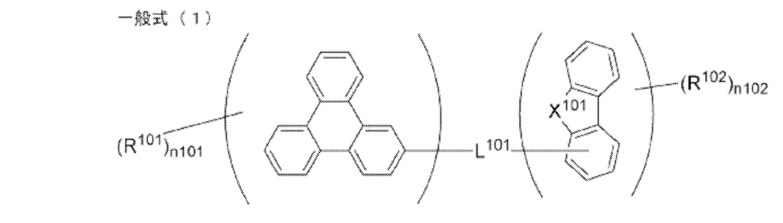
[2] 前記一般式(1)で表される化合物が、下記一般式(2)で表されることを特徴とする[1]に記載の電荷輸送材料。
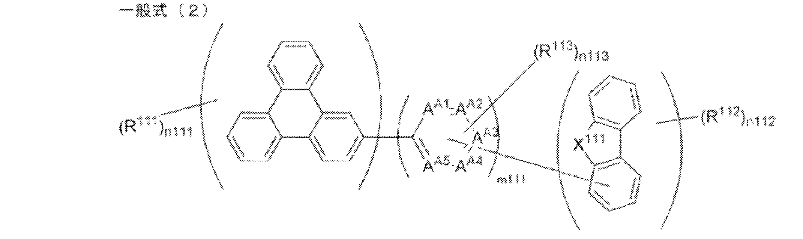
[3] 前記一般式(2)におけるm111が1~5であることを特徴とする[2]に記載の電荷輸送材料。
[4] 前記一般式(1)で表される化合物が、下記一般式(3)で表されることを特徴とする[1]~[3]のいずれか一項に記載の電荷輸送材。

[5] 前記一般式(1)におけるn101が0であることを特徴とする[1]~[4]のいずれか一項に記載の電荷輸送材料。
[6] 前記一般式(1)におけるn102が0~2の整数である、[1]~[5]のいずれか一項に記載の電荷輸送材料。
[7] 前記一般式(1)で表される化合物が、ジベンゾチオフェン骨格およびジベンゾフラン骨格中の酸素原子および硫黄原子を除き、炭素原子および水素原子のみからなることを特徴とする[1]~[6]のいずれか一項に記載の電荷輸送材料。
[8] 前記一般式(1)で表される化合物が、シクロアルキル基を含むことを特徴とする[1]~[7]のいずれか一項に記載の電荷輸送材料。
[9] 一般式(1)で表される化合物の分子量が1200以下である、[1]~[8]のいずれか一項に記載の電荷輸送材料。
[10] 基板と、該基板上に配置され、陽極及び陰極を含む一対の電極と、該電極間に配置された有機層とを有し、前記有機層が、燐光発光材料と[1]~[9]のいずれか一項に記載の電荷輸送材料を含有することを特徴とする有機電界発光素子。
[11] 前記燐光発光材料が下記一般式(E-1)で表されることを特徴とする[10]に記載の有機電界発光素子。
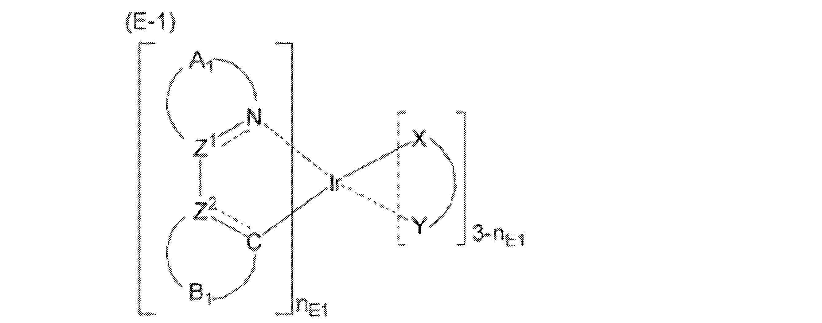
[12] 前記一般式(E-1)で表される燐光発光材料が下記一般式(E-2)で表されることを特徴とする[11]に記載の有機電界発光素子。

[13] 前記一般式(E-1)で表される燐光発光材料の極大発光波長が500nm~700nmであることを特徴とする[11]または[12]記載の有機電界発光素子。
[14] 前記有機層が、前記燐光発光材料を含む発光層とその他の有機層を有し、
前記発光層が前記一般式(1)で表される化合物を含有することを特徴とする[10]~[13]のいずれか一項に記載の有機電界発光素子。
[15] 前記有機層が、前記燐光発光材料を含む発光層とその他の有機層を有し、
該その他の有機層が、前記発光層と前記陰極との間に配置されたホールブロック層を含み、且つ、該ホールブロック層が前記一般式(1)で表される化合物を含有することを特徴とする[10]~[14]のいずれか一項に記載の有機電界発光素子。
[16] [10]~[15]のいずれか一項に記載の有機電界発光素子を用いたことを特徴とする発光装置、表示装置または照明装置。
本発明の電荷輸送材料は、下記一般式(1)で表される化合物からなることを特徴とする。
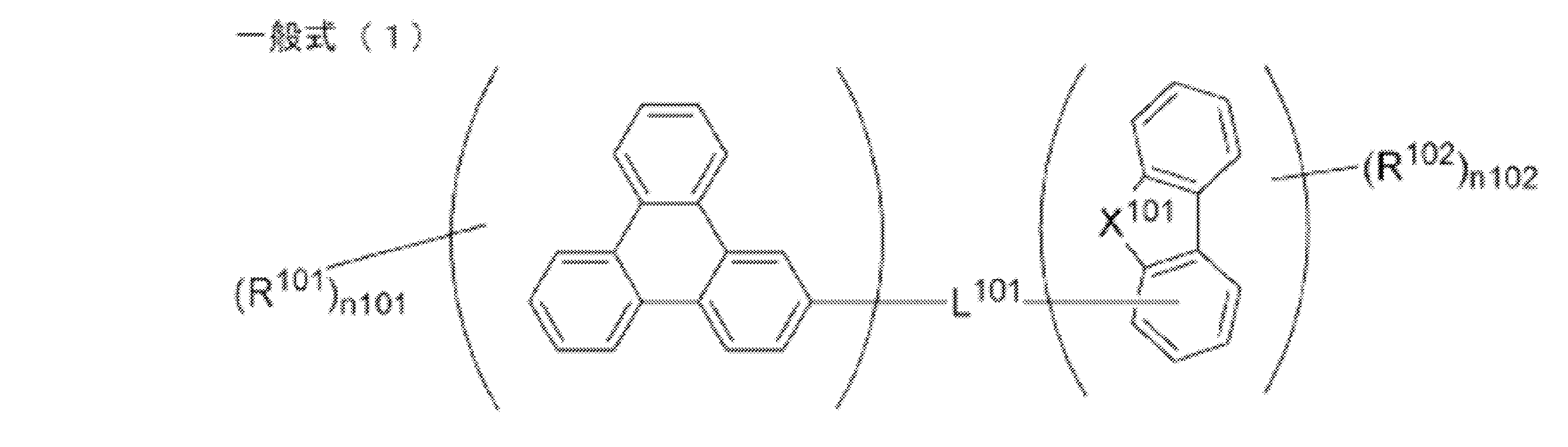
本発明の電荷輸送材料はこのような構成を有することで、いかなる理論に拘泥するものでもないが、フッ素原子、フルオロアルキル基、シクロアルキル基、シクロアルキレン基、シリル基、アルキルシリル基、アリールシリル基またはケイ素原子連結基を導入することで分子間相互作用を適度に抑制させることができる。その結果、膜質の良好な膜が得られ、ダークスポットの発生を抑制することができる。また、本発明者らが検討した結果、これらの置換基は素子の効率や駆動耐久性を損なうことなく、有機膜のTgを高めることができる。そのため、本発明の電荷輸送材料を用いた有機電界発光素子は、高温保管後の効率や駆動耐久性にも優れる。
なお、本発明において、前記一般式(1)の説明における水素原子(H)は同位体(重水素原子(D))も含み、また更に置換基を構成する原子は、その同位体も含んでいることを表す。
本発明において、「置換基」というとき、その置換基は置換されていてもよい。例えば、本発明で「アルキル基」と言う時、フッ素原子で置換されたアルキル基(例えばトリフルオロメチル基)やアリール基で置換されたアルキル基(例えばトリフェニルメチル基)なども含むが、「炭素数1~6のアルキル基」と言うとき、置換されたものも含めた全ての基として炭素数が1~6であることを示す。
本発明において、フッ素原子、フルオロアルキル基、シクロアルキル基、シクロアルキレン基、シリル基、アルキルシリル基、アリールシリル基またはケイ素原子連結基のことを「特定置換基」とも言う。
但し、本明細書中において、「シクロアルキレン基」とは、1,4-シクロヘキサンジイル、1,3-シクロヘキサンジイル、1,2-シクロヘキサンジイル、シクロペンタン等の総称を意味し、シクロアルケンから水素原子を1つ抜き取った環を意味するものではない。
前記R101およびR102としてのアリール基またはヘテロアリール基に、アルキル基、フッ素原子またはシリル基が置換する場合、該置換基としてのアルキル基、ヘテロアリール基、フッ素原子またはシリル基の好ましい範囲は、R101およびR102がアルキル基、ヘテロアリール基、フッ素原子またはシリル基である場合と同様である。前記R101およびR102としてのアリール基またはヘテロアリール基にアルキル基、ヘテロアリール基、フッ素原子またはシリル基が置換する場合、これらの置換基の個数は前記R101およびR102としてのアリール基またはヘテロアリール基に対して1~3個であることが好ましく、1または2個であることがより好ましく、1個であることが特に好ましい。
前記R101およびR102としてのアリール基またはヘテロアリール基に対して、アリール基またはヘテロアリール基が置換する場合、置換によって形成されるアリール基とアリーレン基、または、ヘテロアリール基とヘテロアリーレン基が、いずれも単環どうしであることが好ましく、いずれも6員環の単環であることがより好ましい。

連結置換基(R101)中、AA11~AA20でそれぞれ表される6員環の単環であるアリール基とアリーレン基、または、ヘテロアリール基とヘテロアリーレン基、あるいはそれらの基の組み合わせの好ましい範囲は、さらなる置換基としてアリール基またはヘテロアリール基を有さない以外は、前記一般式(1)におけるR101およびR102としてのアリール基またはヘテロアリール基の好ましい範囲と同様である。
連結置換基(R101)中、R201とR202の好ましい範囲は、前記一般式(1)におけるR101およびR102としてのアルキル基、フッ素原子またはシリル基の好ましい範囲と同様である。
連結置換基(R101)中、m201の好ましい範囲は0または1であり、より好ましくは0である。
連結置換基(R101)中、R201およびR202がアルキル基またはシリル基である場合のn201およびn202の好ましい範囲はそれぞれ独立に0~2であり、より好ましくは0または1である。R201およびR202がフッ素原子である場合のn201およびn202の好ましい範囲はそれぞれ独立に0~3であり、より好ましくは0~2であり、特に好ましくは0または1である。n201およびn202の合計の好ましい範囲は、n101の好ましい範囲と同様である。

連結置換基(R102)中、AA21~AA30で表される6員環の単環であるアリール基とアリーレン基、または、ヘテロアリール基とヘテロアリーレン基の好ましい範囲は、さらなる置換基としてアリール基またはヘテロアリール基を有さない以外は、前記一般式(1)におけるR101およびR102としてのアリール基またはヘテロアリール基の好ましい範囲と同様である。
連結置換基(R102)中、R301とR302の好ましい範囲は、前記一般式(1)におけるR101およびR102としてのアルキル基、フッ素原子またはシリル基の好ましい範囲と同様である。
連結置換基(R102)中、m301の好ましい範囲は0~2の整数であり、より好ましくは0または1であり、特に好ましくは0である。
連結置換基(R102)中、R301およびR302がアルキル基またはシリル基である場合のn301およびn302の好ましい範囲はそれぞれ独立に0~2であり、より好ましくは0または1である。R301およびR302がフッ素原子である場合のn301およびn302の好ましい範囲はそれぞれ独立に0~3であり、より好ましくは0~2であり、特に好ましくは0または1である。n301およびn302の合計の好ましい範囲は、n102の好ましい範囲と同様である。
なお、前記6員環の単環がパラ位で連結する個数の好ましい範囲は、後述するL101についても同様である。
前記一般式(1)においてn101が0ではない場合、前記R101がトリフェニレン環構造に置換する位置については特に制限はないが、前記一般式(1)においてトリフェニレン環が連結基L101と連結している環以外に置換基R101を有することが好ましい。
前記一般式(1)においてn102が0ではない場合、前記R102がジベンゾチオフェンまたはジベンゾフラン構造に置換する位置については特に制限はないが、前記一般式(1)においてジベンゾチオフェンまたはジベンゾフラン構造が連結基L101と連結している環以外に置換基R102を有することが好ましい。
前記一般式(1)におけるL101は、フッ素原子、フルオロアルキル基、シクロアルキル基、シクロアルキレン基、シリル基、アルキルシリル基、アリールシリル基またはケイ素原子連結基(前記特定置換基)のうち、いずれを含む態様でもよいが、本発明では、前記一般式(1)におけるL101がこれらの前記特定置換基のうち、フッ素原子、フルオロアルキル基、シクロアルキル基、アルキルシリル基、アリールシリル基またはケイ素原子連結基を含む態様が好ましく、フッ素原子、フルオロアルキル基またはシクロアルキル基を含む態様がより好ましく、シクロアルキル基を含む態様が特に好ましい。

前記一般式(2)におけるR113は、フッ素原子、フルオロアルキル基、シクロアルキル基、アルキルシリル基またはアリールシリル基を含むことが好ましく、フッ素原子、フルオロアルキル基またはシクロアルキル基を含むことより好ましく、シクロアルキル基を含むことが特に好ましい。これらの各置換基の好ましい範囲は、前記一般式(1)におけるR101で挙げた各置換基の好ましい範囲と同様である。
m111で表される繰り返し単位は、各繰り返し単位中に上述の好ましい範囲の個数のR113を有していてよいが、m111で表される繰り返し単位の全体中、すなわち、前記一般式(1)におけるL111全体中における特定置換基の数が、R113がフッ素原子である場合は0~3であることが好ましく、0~2であることがより好ましく、0または1であることが特に好ましい。R113がアルキル基である場合は0~2であることが好ましく、0または1であることがより好ましく、0であることが特に好ましい。R201およびR202がアリール基、ヘテロアリール基、フルオロアルキル基、アルキルシリル基またはアリールシリル基である場合は、0または1であることが好ましく、0であることがより好ましい。R113がシクロアルキル基である場合は、0または1であることが好ましく、1であることがより好ましい。
m111で表される繰り返し単位は、各繰り返し単位中に上述の好ましい範囲の個数のR113を有しており、m111で表される繰り返し単位全体において上述の好ましい範囲の個数のR113を有していることが好ましい。但し、前記特定置換基がフッ素原子である場合は、この限りではない。

前記一般式(3)におけるR123、m121およびn123の好ましい範囲は、前記一般式(2)におけるR113、m111およびn113の好ましい範囲とそれぞれ同じである。


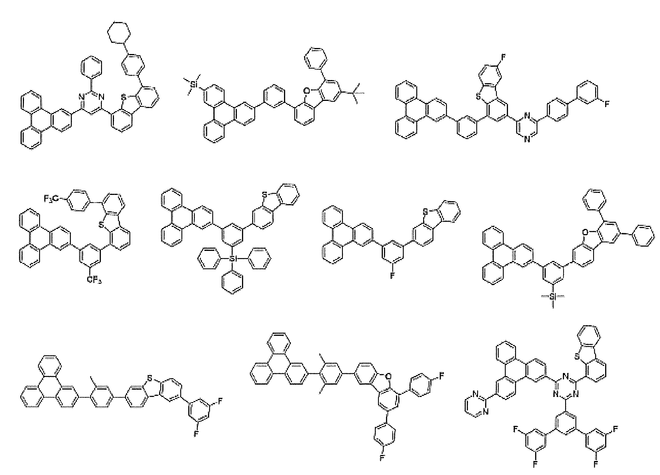
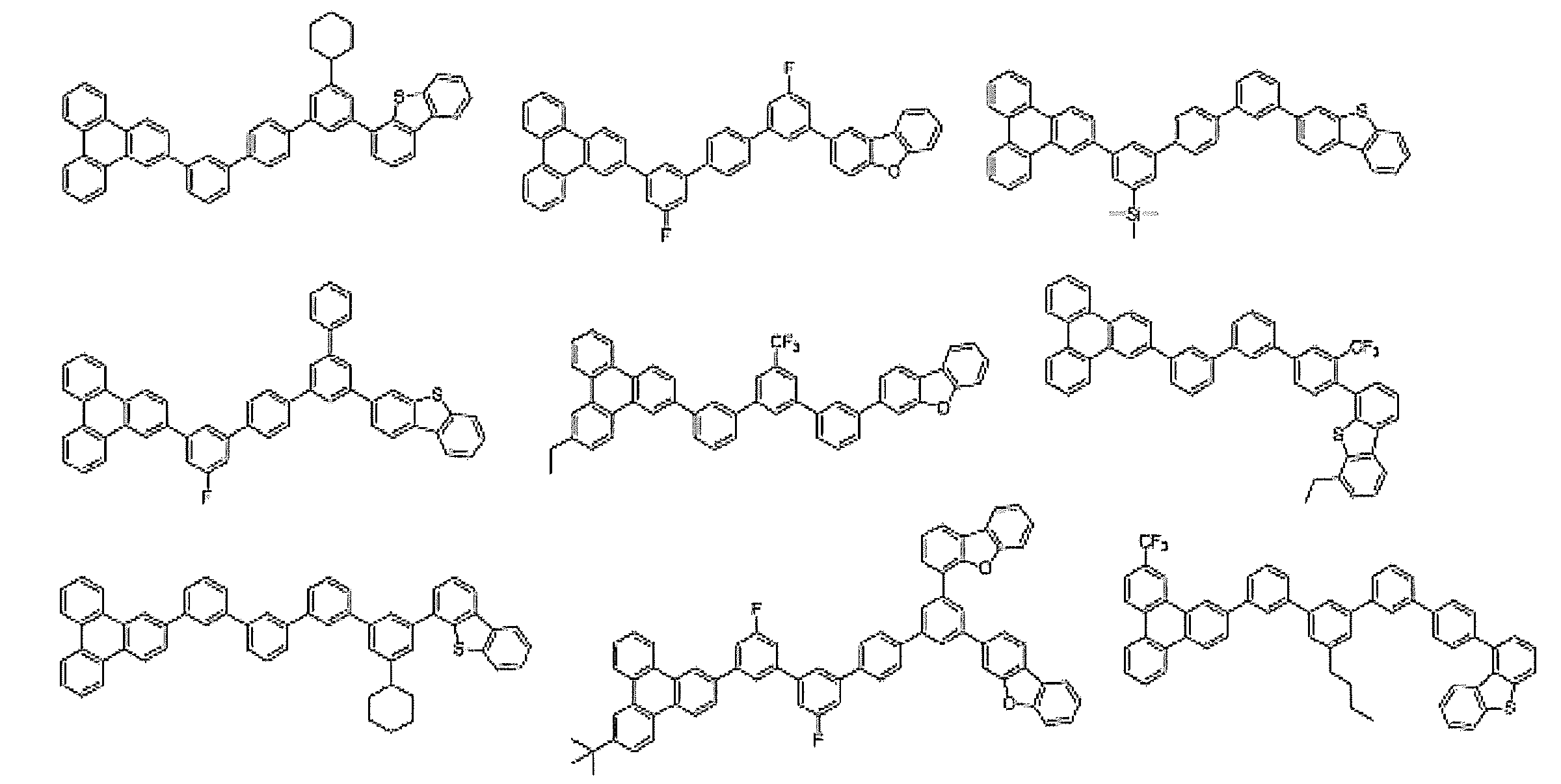


合成後、カラムクロマトグラフィー、再結晶等による精製を行った後、昇華精製により精製することが好ましい。昇華精製により、有機不純物を分離できるだけでなく、無機塩や残留溶媒等を効果的に取り除くことができる。
本発明の有機電界発光素子は、基板と、該基板上に配置され、陽極及び陰極を含む一対の電極と、該電極間に配置された有機層とを有し、前記有機層が、燐光発光材料と本発明の電荷輸送材料、すなわち前記一般式(1)で表される化合物を含むことを特徴とする。

有機電界発光素子の素子構成、基板、陰極及び陽極については、例えば、特開2008-270736号公報に詳述されており、該公報に記載の事項を本発明に適用することができる。
以下、本発明の有機電界発光素子の好ましい態様について、基板、電極、有機層、保護層、封止容器、駆動方法、発光波長、用途の順で詳細に説明する。
本発明の有機電界発光素子は、基板を有する。
本発明で使用する基板としては、有機層から発せられる光を散乱又は減衰させない基板であることが好ましい。有機材料の場合には、耐熱性、寸法安定性、耐溶剤性、電気絶縁性、及び加工性に優れていることが好ましい。
本発明の有機電界発光素子は、前記基板上に配置され、陽極及び陰極を含む一対の電極を有する。
発光素子の性質上、一対の電極である陽極及び陰極のうち少なくとも一方の電極は、透明若しくは半透明であることが好ましい。
陽極は、通常、有機層に正孔を供給する電極としての機能を有していればよく、その形状、構造、大きさ等については特に制限はなく、発光素子の用途、目的に応じて、公知の電極材料の中から適宜選択することができる。前述のごとく、陽極は、通常透明陽極として設けられる。
陰極は、通常、有機層に電子を注入する電極としての機能を有していればよく、その形状、構造、大きさ等については特に制限はなく、発光素子の用途、目的に応じて、公知の電極材料の中から適宜選択することができる。
本発明の有機電界発光素子は、前記電極間に配置された有機層を有し、前記有機層が、燐光発光材料と前記一般式(1)で表される化合物を含むことを特徴とする。
前記有機層は、特に制限はなく、有機電界発光素子の用途、目的に応じて適宜選択することができるが、前記透明電極上に又は前記半透明電極上に形成されるのが好ましい。この場合、有機層は、前記透明電極又は前記半透明電極上の全面又は一面に形成される。
有機層の形状、大きさ、及び厚み等については、特に制限はなく、目的に応じて適宜選択することができる。
以下、本発明の有機電界発光素子における、有機層の構成、有機層の形成方法、有機層を構成する各層の好ましい態様および各層に使用される材料について順に説明する。
本発明の有機電界発光素子では、前記有機層が、電荷輸送層を含むことが好ましい。前記電荷輸送層とは、有機電界発光素子に電圧を印加した際に電荷移動が起こる層をいう。具体的には正孔注入層、正孔輸送層、電子ブロック層、発光層、正孔ブロック層、電子輸送層又は電子注入層が挙げられる。前記電荷輸送層が正孔注入層、正孔輸送層、電子ブロック層又は発光層であれば、低コストかつ高効率な有機電界発光素子の製造が可能となる。
本発明の有機電界発光素子では、前記燐光発光材料を含む発光層とその他の有機層を有し、前記発光層が前記一般式(1)で表される化合物を含有することが好ましい。さらに、本発明の有機電界発光素子では、前記有機層が、前記燐光発光材料を含む発光層とその他の有機層を有すことがより好ましい。但し、本発明の有機電界発光素子は、前記有機層が発光層とその他の有機層を有する場合であっても、必ずしも明確に層間が区別されなくてもよい。
前記一般式(1)で表される化合物を含有してもよい有機層としては、発光層、正孔注入層、正孔輸送層、電子輸送層、電子注入層、励起子ブロック層、電荷ブロック層(正孔ブロック層、電子ブロック層など)などを挙げることができ、好ましくは、発光層、励起子ブロック層、電荷ブロック層、電子輸送層、電子注入層のいずれかであり、より好ましくは発光層、励起子ブロック層、電荷ブロック層、又は電子輸送層であり、更に好ましくは発光層又は正孔ブロック層である。
前記一般式(1)で表される化合物は、発光層以外の有機層に含有される場合、該有機層の全質量に対して70~100質量%含まれることが好ましく、85~100質量%含まれることがより好ましい。
本発明の有機電界発光素子において、各有機層は、蒸着法やスパッタ法等の乾式製膜法、転写法、印刷法、スピンコート法、バーコート法等の湿式製膜法(溶液塗布法)のいずれによっても好適に形成することができる。
本発明の有機電界発光素子は、前記一対の電極間に配置された有機層が、少なくとも一層の前記一般式(1)で表される化合物を含む組成物の蒸着により形成された層を含むことが好ましい。
発光層は、電界印加時に、陽極、正孔注入層又は正孔輸送層から正孔を受け取り、陰極、電子注入層又は電子輸送層から電子を受け取り、正孔と電子の再結合の場を提供して発光させる機能を有する層である。但し、本発明における前記発光層は、このようなメカニズムによる発光に必ずしも限定されるものではない。本発明の有機電界発光素子における発光層は、少なくとも一種の燐光発光材料を含有することが好ましい。
以下、前記発光層の材料として、前記発光材料、前記一般式(1)で表される化合物以外のその他のホスト材料について順に説明する。なお、前記一般式(1)で表される化合物は、本発明の有機電界発光素子において前記発光層以外に用いられてもよい。
本発明における発光材料としては、燐光発光材料、蛍光発光材料等いずれも用いることができる。
本発明における発光層は、色純度を向上させるためや発光波長領域を広げるために2種類以上の発光材料を含有することができる。発光材料の少なくとも一種が燐光発光材料であることが好ましい。
本発明では、発光層に含有される少なくとも一種の燐光発光材料に加えて、発光材料として、蛍光発光材料や、発光層に含有される燐光発光材料とは異なる燐光発光材料を用いることができる。
これら蛍光発光材料や燐光発光材料については、例えば、特開2008-270736号公報の段落番号[0100]~[0164]、特開2007-266458号公報の段落番号[0088]~[0090]に詳述されており、これら公報の記載の事項を本発明に適用することができる。
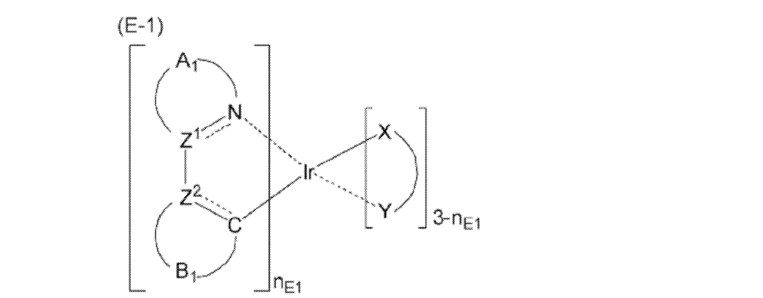
A1はZ1と窒素原子と共に5又は6員のヘテロ環を形成する原子群を表す。
B1はZ2と炭素原子と共に5又は6員環を形成する原子群を表す。
(X-Y)はモノアニオン性の二座配位子を表す。
nE1は1~3の整数を表す。nE1が2または3の場合、Z1、Z2、A1及びB1を含む配位子が2つまたは3つ存在することになるが、2つまたは3つ存在する該配位子は互いに同じであっても異なっていてもよい。
Z1及びZ2はそれぞれ独立に、炭素原子又は窒素原子を表す。Z1及びZ2として好ましくは炭素原子である。
錯体の安定性、発光波長制御及び発光量子収率の観点から、A1、Z1及び窒素原子で形成される5又は6員のヘテロ環として好ましくは、ピリジン環、ピラジン環、イミダゾール環、ピラゾール環であり、より好ましくはピリジン環、イミダゾール環、ピラジン環であり、更に好ましくはピリジン環、イミダゾール環であり、最も好ましくはピリジン環である。
アルキル基(好ましくは炭素数1~30、より好ましくは炭素数1~20、特に好ましくは炭素数1~10であり、例えばメチル、エチル、イソプロピル、t-ブチル、n-オクチル、n-デシル、n-ヘキサデシル、シクロプロピル、シクロペンチル、シクロヘキシルなどが挙げられる。)、アルケニル基(好ましくは炭素数2~30、より好ましくは炭素数2~20、特に好ましくは炭素数2~10であり、例えばビニル、アリル、2-ブテニル、3-ペンテニルなどが挙げられる。)、アルキニル基(好ましくは炭素数2~30、より好ましくは炭素数2~20、特に好ましくは炭素数2~10であり、例えばプロパルギル、3-ペンチニルなどが挙げられる。)、アリール基(好ましくは炭素数6~30、より好ましくは炭素数6~20、特に好ましくは炭素数6~12であり、例えばフェニル、p-メチルフェニル、ナフチル、アントリルなどが挙げられる。)、アミノ基(好ましくは炭素数0~30、より好ましくは炭素数0~20、特に好ましくは炭素数0~10であり、例えばアミノ、メチルアミノ、ジメチルアミノ、ジエチルアミノ、ジベンジルアミノ、ジフェニルアミノ、ジトリルアミノなどが挙げられる。)、アルコキシ基(好ましくは炭素数1~30、より好ましくは炭素数1~20、特に好ましくは炭素数1~10であり、例えばメトキシ、エトキシ、ブトキシ、2-エチルヘキシロキシなどが挙げられる。)、アリールオキシ基(好ましくは炭素数6~30、より好ましくは炭素数6~20、特に好ましくは炭素数6~12であり、例えばフェニルオキシ、1-ナフチルオキシ、2-ナフチルオキシなどが挙げられる。)、ヘテロ環オキシ基(好ましくは炭素数1~30、より好ましくは炭素数1~20、特に好ましくは炭素数1~12であり、例えばピリジルオキシ、ピラジニルオキシ、ピリミジニルオキシ、キノリルオキシなどが挙げられる。)、アシル基(好ましくは炭素数2~30、より好ましくは炭素数2~20、特に好ましくは炭素数2~12であり、例えばアセチル、ベンゾイル、ホルミル、ピバロイルなどが挙げられる。)、アルコキシカルボニル基(好ましくは炭素数2~30、より好ましくは炭素数2~20、特に好ましくは炭素数2~12であり、例えばメトキシカルボニル、エトキシカルボニルなどが挙げられる。)、アリールオキシカルボニル基(好ましくは炭素数7~30、より好ましくは炭素数7~20、特に好ましくは炭素数7~12であり、例えばフェニルオキシカルボニルなどが挙げられる。)、アシルオキシ基(好ましくは炭素数2~30、より好ましくは炭素数2~20、特に好ましくは炭素数2~10であり、例えばアセトキシ、ベンゾイルオキシなどが挙げられる。)、アシルアミノ基(好ましくは炭素数2~30、より好ましくは炭素数2~20、特に好ましくは炭素数2~10であり、例えばアセチルアミノ、ベンゾイルアミノなどが挙げられる。)、アルコキシカルボニルアミノ基(好ましくは炭素数2~30、より好ましくは炭素数2~20、特に好ましくは炭素数2~12であり、例えばメトキシカルボニルアミノなどが挙げられる。)、アリールオキシカルボニルアミノ基(好ましくは炭素数7~30、より好ましくは炭素数7~20、特に好ましくは炭素数7~12であり、例えばフェニルオキシカルボニルアミノなどが挙げられる。)、スルホニルアミノ基(好ましくは炭素数1~30、より好ましくは炭素数1~20、特に好ましくは炭素数1~12であり、例えばメタンスルホニルアミノ、ベンゼンスルホニルアミノなどが挙げられる。)、スルファモイル基(好ましくは炭素数0~30、より好ましくは炭素数0~20、特に好ましくは炭素数0~12であり、例えばスルファモイル、メチルスルファモイル、ジメチルスルファモイル、フェニルスルファモイルなどが挙げられる。)、カルバモイル基(好ましくは炭素数1~30、より好ましくは炭素数1~20、特に好ましくは炭素数1~12であり、例えばカルバモイル、メチルカルバモイル、ジエチルカルバモイル、フェニルカルバモイルなどが挙げられる。)、アルキルチオ基(好ましくは炭素数1~30、より好ましくは炭素数1~20、特に好ましくは炭素数1~12であり、例えばメチルチオ、エチルチオなどが挙げられる。)、アリールチオ基(好ましくは炭素数6~30、より好ましくは炭素数6~20、特に好ましくは炭素数6~12であり、例えばフェニルチオなどが挙げられる。)、ヘテロ環チオ基(好ましくは炭素数1~30、より好ましくは炭素数1~20、特に好ましくは炭素数1~12であり、例えばピリジルチオ、2-ベンズイミゾリルチオ、2-ベンズオキサゾリルチオ、2-ベンズチアゾリルチオなどが挙げられる。)、スルホニル基(好ましくは炭素数1~30、より好ましくは炭素数1~20、特に好ましくは炭素数1~12であり、例えばメシル、トシルなどが挙げられる。)、スルフィニル基(好ましくは炭素数1~30、より好ましくは炭素数1~20、特に好ましくは炭素数1~12であり、例えばメタンスルフィニル、ベンゼンスルフィニルなどが挙げられる。)、ウレイド基(好ましくは炭素数1~30、より好ましくは炭素数1~20、特に好ましくは炭素数1~12であり、例えばウレイド、メチルウレイド、フェニルウレイドなどが挙げられる。)、リン酸アミド基(好ましくは炭素数1~30、より好ましくは炭素数1~20、特に好ましくは炭素数1~12であり、例えばジエチルリン酸アミド、フェニルリン酸アミドなどが挙げられる。)、ヒドロキシ基、メルカプト基、ハロゲン原子(例えばフッ素原子、塩素原子、臭素原子、ヨウ素原子)、シアノ基、スルホ基、カルボキシル基、ニトロ基、ヒドロキサム酸基、スルフィノ基、ヒドラジノ基、イミノ基、ヘテロ環基(ヘテロアリール基も包含し、好ましくは炭素数1~30、より好ましくは炭素数1~12であり、ヘテロ原子としては、例えば窒素原子、酸素原子、硫黄原子、リン原子、ケイ素原子、セレン原子、テルル原子であり、具体的にはピリジル、ピラジニル、ピリミジニル、ピリダジニル、ピロリル、ピラゾリル、トリアゾリル、イミダゾリル、オキサゾリル、チアゾリル、イソキサゾリル、イソチアゾリル、キノリル、フリル、チエニル、セレノフェニル、テルロフェニル、ピペリジル、ピペリジノ、モルホリノ、ピロリジル、ピロリジノ、ベンゾオキサゾリル、ベンゾイミダゾリル、ベンゾチアゾリル、カルバゾリル基、アゼピニル基、シロリル基などが挙げられる。)、シリル基(好ましくは炭素数3~40、より好ましくは炭素数3~30、特に好ましくは炭素数3~24であり、例えばトリメチルシリル、トリフェニルシリルなどが挙げられる。)、シリルオキシ基(好ましくは炭素数3~40、より好ましくは炭素数3~30、特に好ましくは炭素数3~24であり、例えばトリメチルシリルオキシ、トリフェニルシリルオキシなどが挙げられる。)、ホスホリル基(例えばジフェニルホスホリル基、ジメチルホスホリル基などが挙げられる。)が挙げられる。これらの置換基は更に置換されてもよく、更なる置換基としては、以上に説明した置換基群Aから選択される基を挙げることができる。また、置換基に置換した置換基は更に置換されてもよく、さらなる置換基としては、以上に説明した置換基群Aから選択される基を挙げることができる。また、置換基に置換した置換基に置換した置換基は更に置換されてもよく、さらなる置換基としては、以上に説明した置換基群Aから選択される基を挙げることができる。
アルキル基(好ましくは炭素数1~30、より好ましくは炭素数1~20、特に好ましくは炭素数1~10であり、例えばメチル、エチル、イソプロピル、t-ブチル、n-オクチル、n-デシル、n-ヘキサデシル、シクロプロピル、シクロペンチル、シクロヘキシルなどが挙げられる。)、アルケニル基(好ましくは炭素数2~30、より好ましくは炭素数2~20、特に好ましくは炭素数2~10であり、例えばビニル、アリル、2-ブテニル、3-ペンテニルなどが挙げられる。)、アルキニル基(好ましくは炭素数2~30、より好ましくは炭素数2~20、特に好ましくは炭素数2~10であり、例えばプロパルギル、3-ペンチニルなどが挙げられる。)、アリール基(好ましくは炭素数6~30、より好ましくは炭素数6~20、特に好ましくは炭素数6~12であり、例えばフェニル、p-メチルフェニル、ナフチル、アントリルなどが挙げられる。)、シアノ基、ヘテロ環基(ヘテロアリール基も包含し、好ましくは炭素数1~30、より好ましくは炭素数1~12であり、ヘテロ原子としては、例えば窒素原子、酸素原子、硫黄原子、リン原子、ケイ素原子、セレン原子、テルル原子であり、具体的にはピリジル、ピラジニル、ピリミジニル、ピリダジニル、ピロリル、ピラゾリル、トリアゾリル、イミダゾリル、オキサゾリル、チアゾリル、イソキサゾリル、イソチアゾリル、キノリル、フリル、チエニル、セレノフェニル、テルロフェニル、ピペリジル、ピペリジノ、モルホリノ、ピロリジル、ピロリジノ、ベンゾオキサゾリル、ベンゾイミダゾリル、ベンゾチアゾリル、カルバゾリル基、アゼピニル基、シロリル基などが挙げられる。)これらの置換基は更に置換されてもよく、更なる置換基としては、前記置換基群Bから選択される基を挙げることができる。また、置換基に置換した置換基は更に置換されてもよく、さらなる置換基としては、以上に説明した置換基群Bから選択される基を挙げることができる。また、置換基に置換した置換基に置換した置換基は更に置換されてもよく、さらなる置換基としては、以上に説明した置換基群Bから選択される基を挙げることができる。
前記置換基同士は連結して縮合環を形成していてもよく、形成される環としては、ベンゼン環、ピリジン環、ピラジン環、ピリダジン環、ピリミジン環、イミダゾール環、オキサゾール環、チアゾール環、ピラゾール環、チオフェン環、フラン環などが挙げられる。これら形成される環は置換基を有していてもよく、置換基としては前述の炭素原子上の置換基、窒素原子上の置換基が挙げられる。
錯体の安定性、発光波長制御及び発光量子収率の観点からB1、Z2及び炭素原子で形成される5又は6員環として好ましくは、ベンゼン環、ピリジン環、ピラジン環、イミダゾール環、ピラゾール環、チオフェン環であり、より好ましくはベンゼン環、ピリジン環、ピラゾール環であり、更に好ましくはベンゼン環、ピリジン環である。
また前記A1、Z1及び窒素原子で形成される5又は6員のヘテロ環の置換基と、前記B1、Z2及び炭素原子で形成される5又は6員環の置換基とが連結して、前述と同様の縮合環を形成していてもよい。
(X-Y)で表される配位子としては下記一般式(l-1)~(l-13)が好ましいが、本発明はこれらに限定されない。

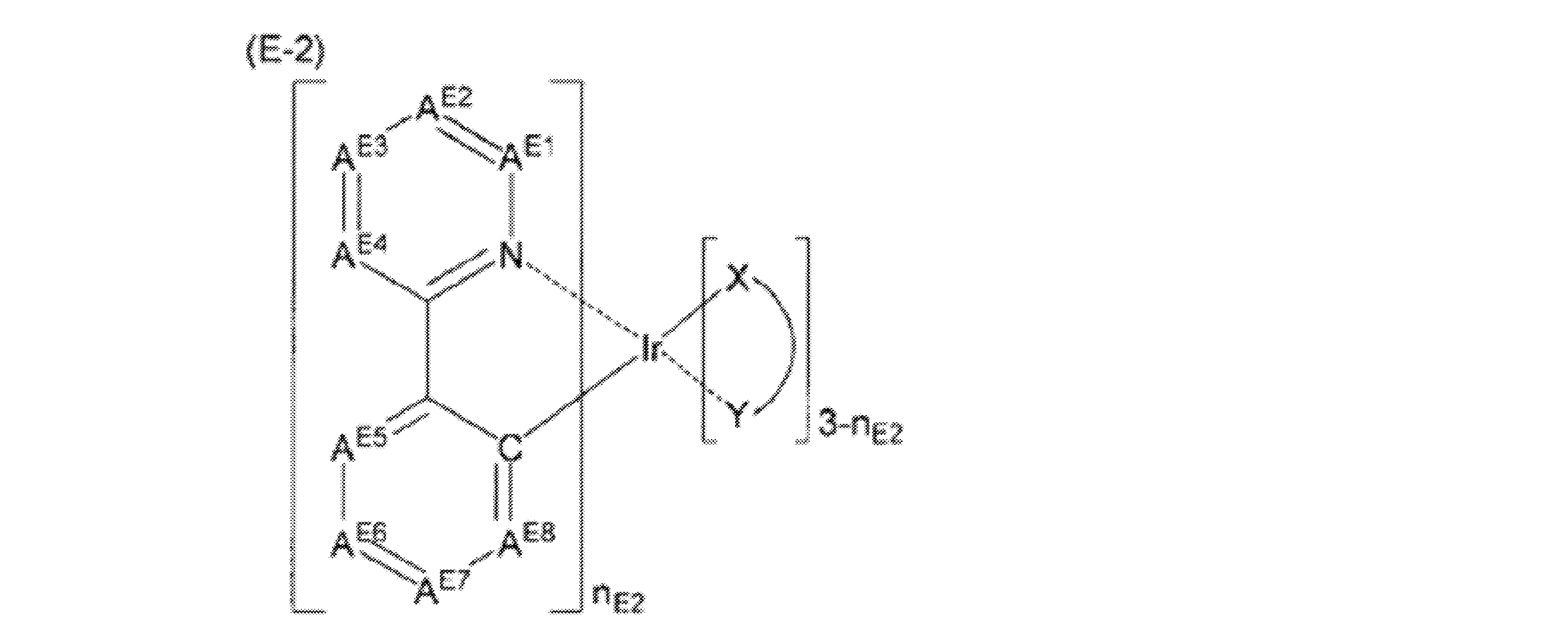
REは水素原子又は置換基を表す。
(X-Y)はモノアニオン性の二座配位子を表す。
nE2は1~3の整数を表す。
AE1~AE4として好ましくはC-REであり、AE1~AE4がC-REである場合に、AE3のREとして好ましくは水素原子、アルキル基、アリール基、アミノ基、アルコキシ基、アリールオキシ基、フッ素原子、又はシアノ基であり、より好ましくは水素原子、アルキル基、アミノ基、アルコキシ基、アリールオキシ基、又はフッ素原子であり、特に好ましく水素原子、又はフッ素原子であり、AE1、AE2及びAE4のREとして好ましくは水素原子、アルキル基、アリール基、アミノ基、アルコキシ基、アリールオキシ基、フッ素原子、又はシアノ基であり、より好ましくは水素原子、アルキル基、アミノ基、アルコキシ基、アリールオキシ基、又はフッ素原子であり、特に好ましく水素原子である。
(X-Y)、及びnE2は一般式(E-1)における(X-Y)、及びnE1と同義であり好ましい範囲も同様である。

AはCR'又は窒素原子を表し、R'は水素原子、アルキル基、シクロアルキル基、アルケニル基、アルキニル基、-CN、ペルフルオロアルキル基、トリフルオロビニル基、-CO2R、-C(O)R、-NR2、-NO2、-OR、ハロゲン原子、アリール基又はヘテロアリール基を表し、更に置換基を有していてもよい。Rはそれぞれ独立に、水素原子、アルキル基、ペルハロアルキル基、アルケニル基、アルキニル基、ヘテロアルキル基、アリール基又はヘテロアリール基を表す。
RT1~RT7、及びR'は、任意の2つが互いに結合して縮合4~7員環を形成してもよく、該縮合4~7員環は、シクロアルキル、アリール又はヘテロアリールであり、該縮合4~7員環は更に置換基を有していてもよい。これらのうち、RT1とRT7、又はRT5とRT6で縮環してベンゼン環を形成する場合が好ましく、RT5とRT6で縮環してベンゼン環を形成する場合が特に好ましい。
(X-Y)は、モノアニオン性の二座配位子を表す。nE3は1~3の整数を表す。
シクロアルキル基としては、置換基を有していてもよく、飽和であっても不飽和であってもよく、置換してもよい基としては、前述の置換基Aを挙げることができる。RT1~RT7、及びR'で表されるシクロアルキル基として、好ましくは環員数4~7のシクロアルキル基であり、より好ましくは総炭素原子数5~6のシクロアルキル基であり、例えばシクロペンチル基、シクロヘキシル基等が挙げられる。
RT1~RT7、及びR'で表されるアルケニル基としては好ましくは炭素数2~30、より好ましくは炭素数2~20、特に好ましくは炭素数2~10であり、例えばビニル、アリル、1-プロペニル、1-イソプロペニル、1-ブテニル、2-ブテニル、3-ペンテニルなどが挙げられる。
RT1~RT7、及びR'で表されるアルキニル基としては、好ましくは炭素数2~30、より好ましくは炭素数2~20、特に好ましくは炭素数2~10であり、例えばエチニル、プロパルギル、1-プロピニル、3-ペンチニルなどが挙げられる。
またAがCR'を表すと共に、RT1~RT7、及びR'のうち、0~2つがアルキル基又はフェニル基で、残りが全て水素原子である場合が特に好ましく、RT1~RT7、及びR'のうち、0~2つがアルキル基で、残りが全て水素原子である場合が特に好ましく、RT1~RT7、及びR'のうち、0~2つがメチル基で、残りが全て水素原子である場合が最も好ましい。
(X-Y)は、一般式(E-1)における(X-Y)と同義であり好ましい範囲も同様である。

R1'~R5'は、任意の2つが互いに結合して縮合4~7員環を形成してもよく、該縮合4~7員環は、シクロアルキル、アリール又はヘテロアリールであり、該縮合4~7員環は更に置換基を有していてもよい。
また、R1'~R5'における好ましい範囲は、一般式(E-3)におけるRT1~RT7、R'と同様である。またAがCR'を表すと共に、RT1~RT4、R'、及びR1'~R5'のうち、0~2つがアルキル基又はフェニル基で残りが全て水素原子である場合が特に好ましく、RT1~RT4、R'、及びR1'~R5'のうち、0~2つがアルキル基で残りが全て水素原子である場合が更に好ましい。
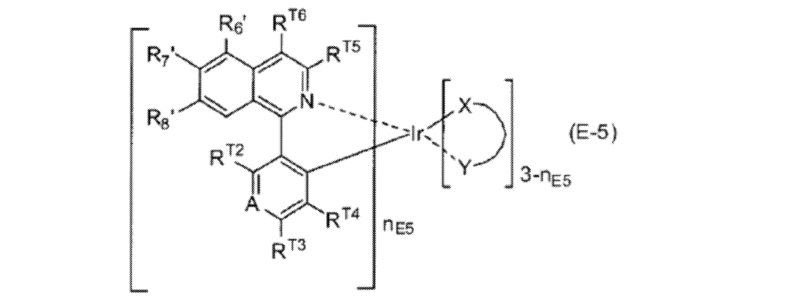
RT5、RT6、R6'~R8'は、任意の2つが互いに結合して縮合4~7員環を形成してもよく、該縮合4~7員環は、シクロアルキル、アリール又はヘテロアリールであり、該縮合4~7員環は更に置換基を有していてもよい。
また、R6'~R8'における好ましい範囲は、一般式(E-3)におけるRT1~RT7、R'と同様である。またAがCR'を表すと共に、RT2~RT6、R'、及びR6'~R8'のうち、0~2つがアルキル基又はフェニル基で残りが全て水素原子である場合が特に好ましく、RT2~RT6、R'、及びR6'~R8'のうち、0~2つがアルキル基で残りが全て水素原子である場合が更に好ましい。
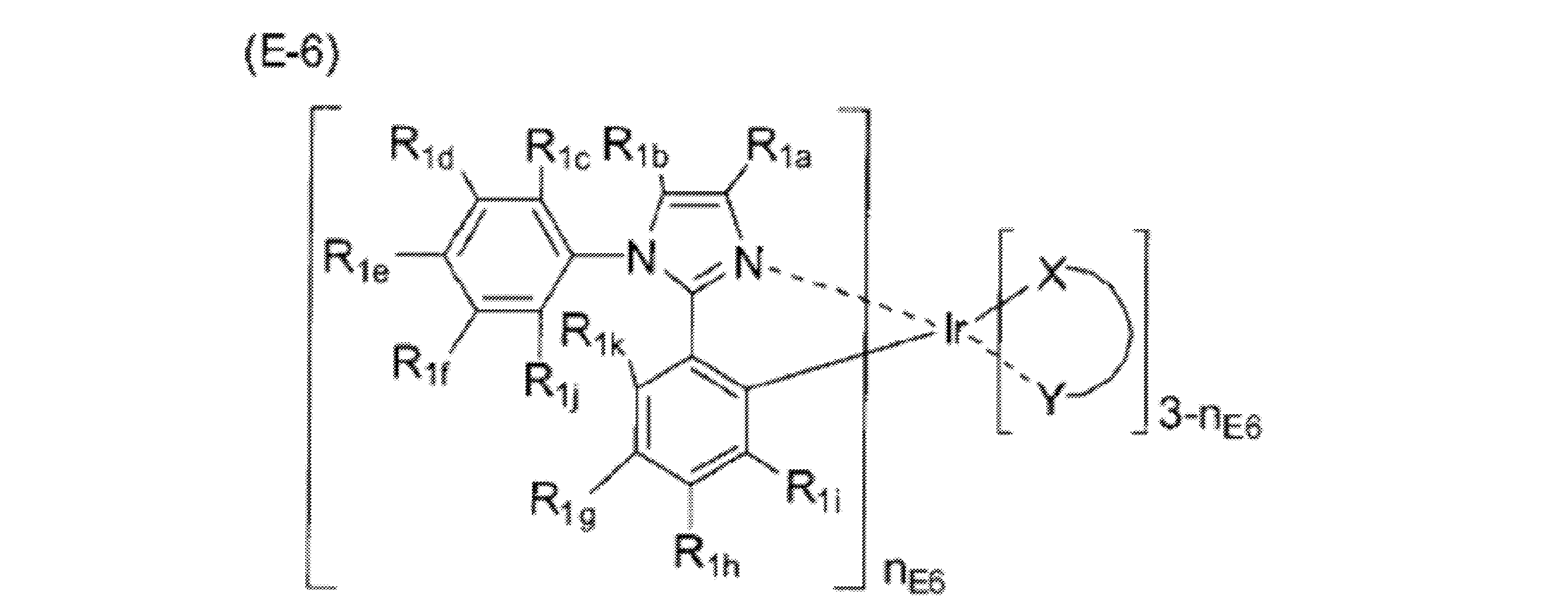
R1a~R1kは、任意の2つが互いに結合して縮合4~7員環を形成してもよく、該縮合4~7員環は、シクロアルキル、アリール又はヘテロアリールであり、該縮合4~7員環は更に置換基を有していてもよい。
(X-Y)は、モノアニオン性の二座配位子を表す。
nE6は1~3の整数を表す。
R1jとR1kとが連結し単結合を形成する場合が特に好ましい。
(X-Y)、及びnE6の好ましい範囲は、一般式(E-3)における(X-Y)、及びnE3と同様である。

R1a~R1kは、任意の2つが互いに結合して縮合4~7員環を形成してもよく、該縮合4~7員環は、シクロアルキル基、アリール基又はヘテロアリール基であり、該縮合4~7員環は更に置換基を有していてもよい。
(X-Y)は、モノアニオン性の二座配位子を表す。
nE7は1~3の整数を表す。
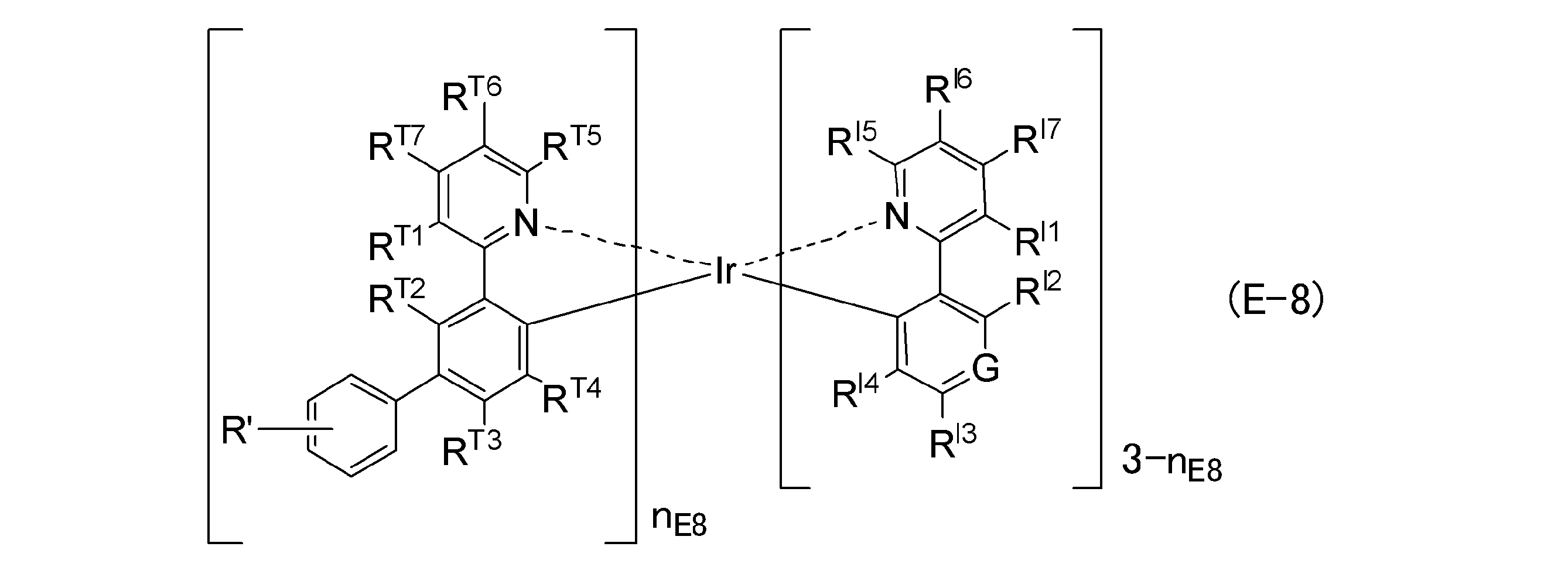

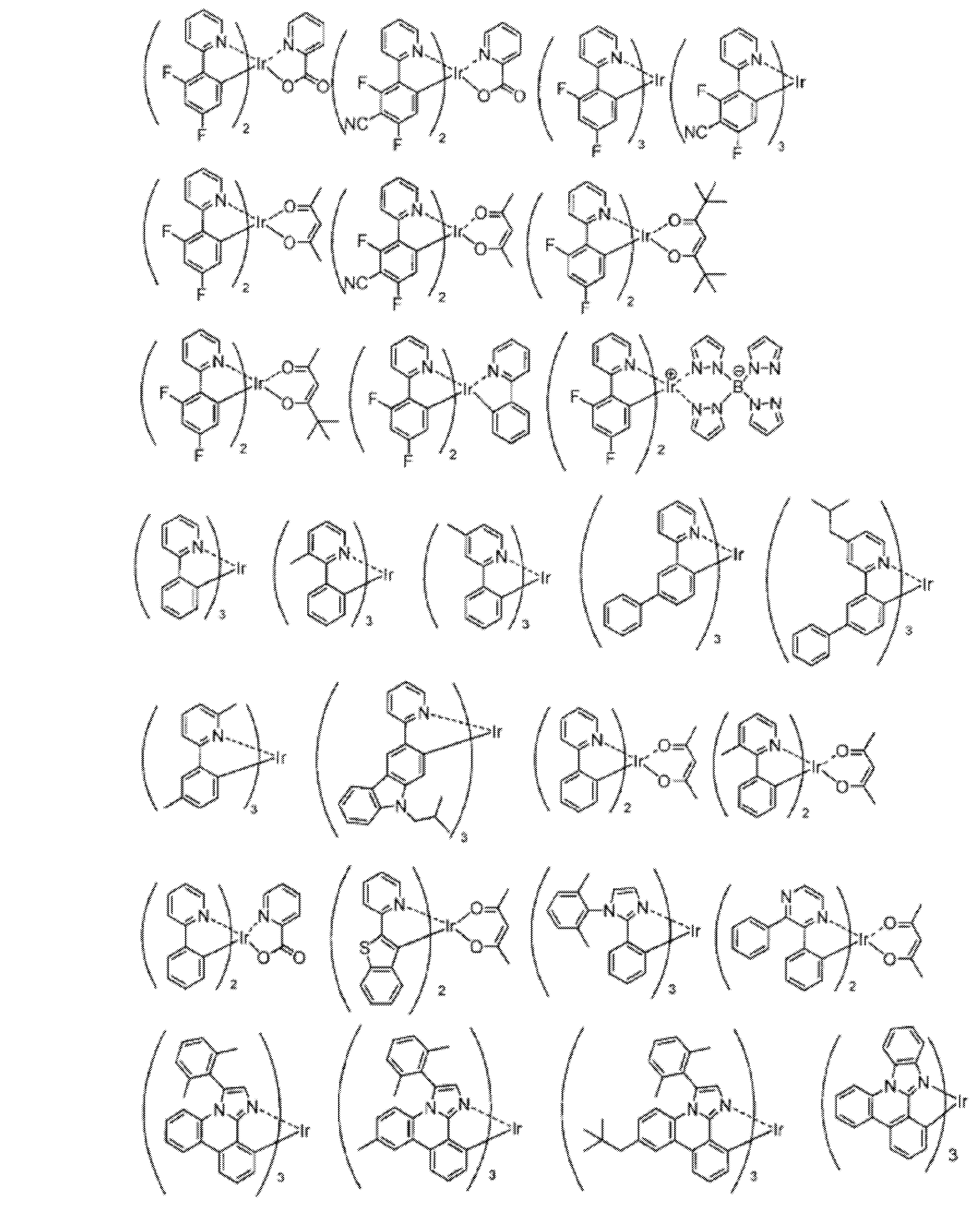
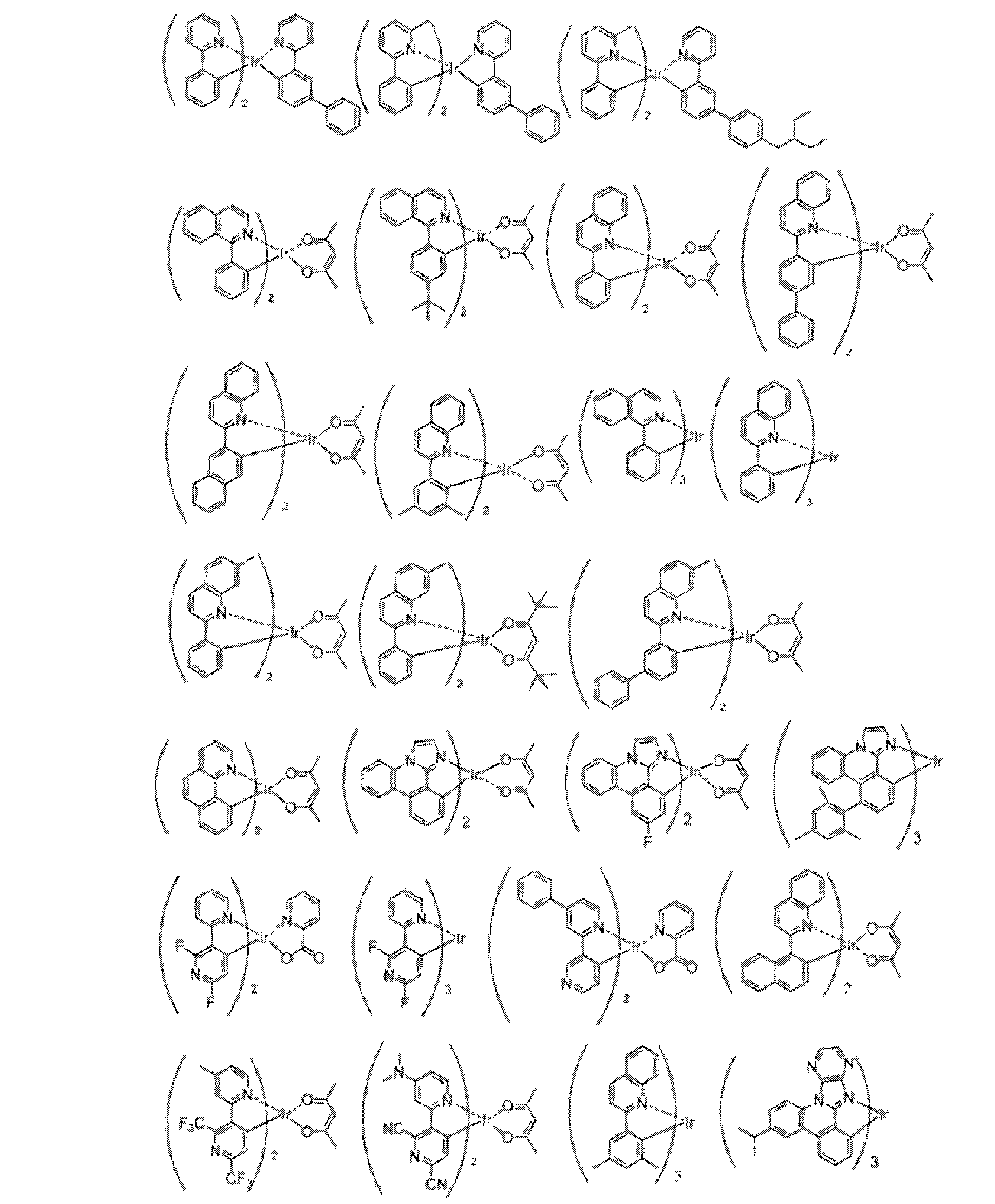
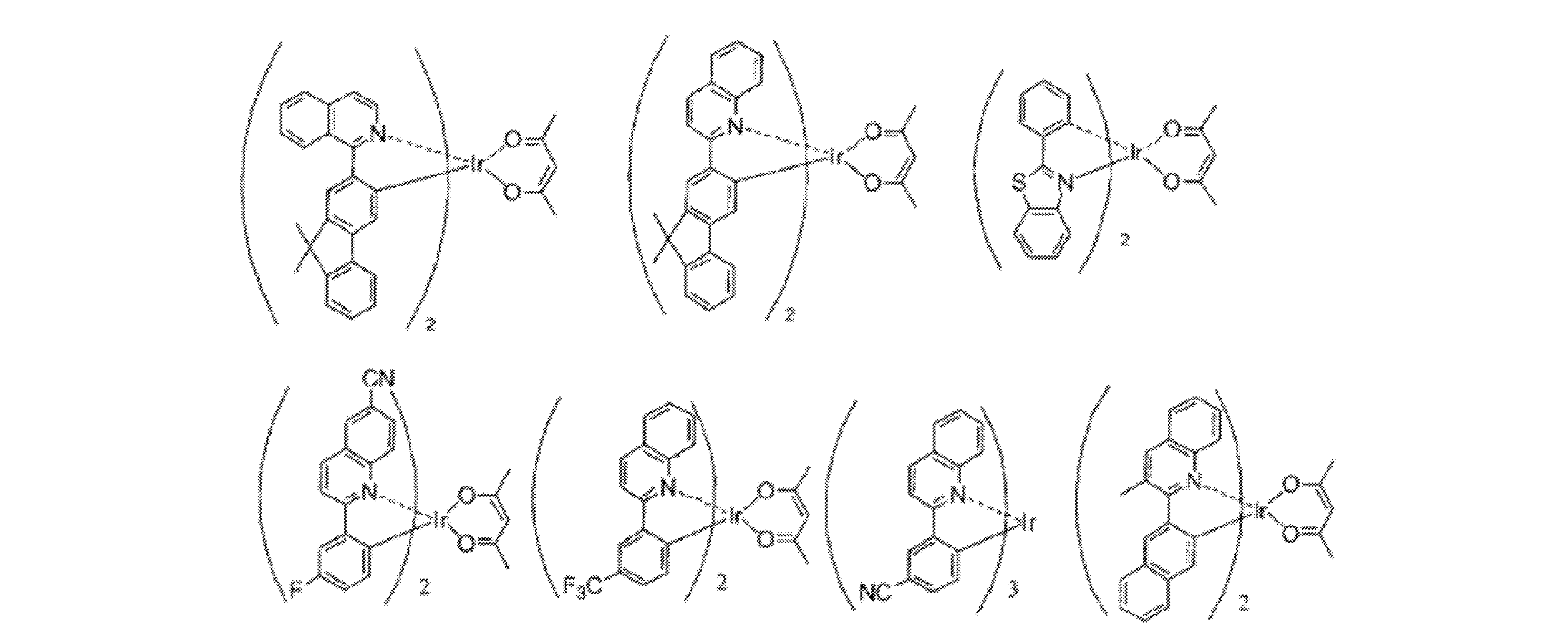
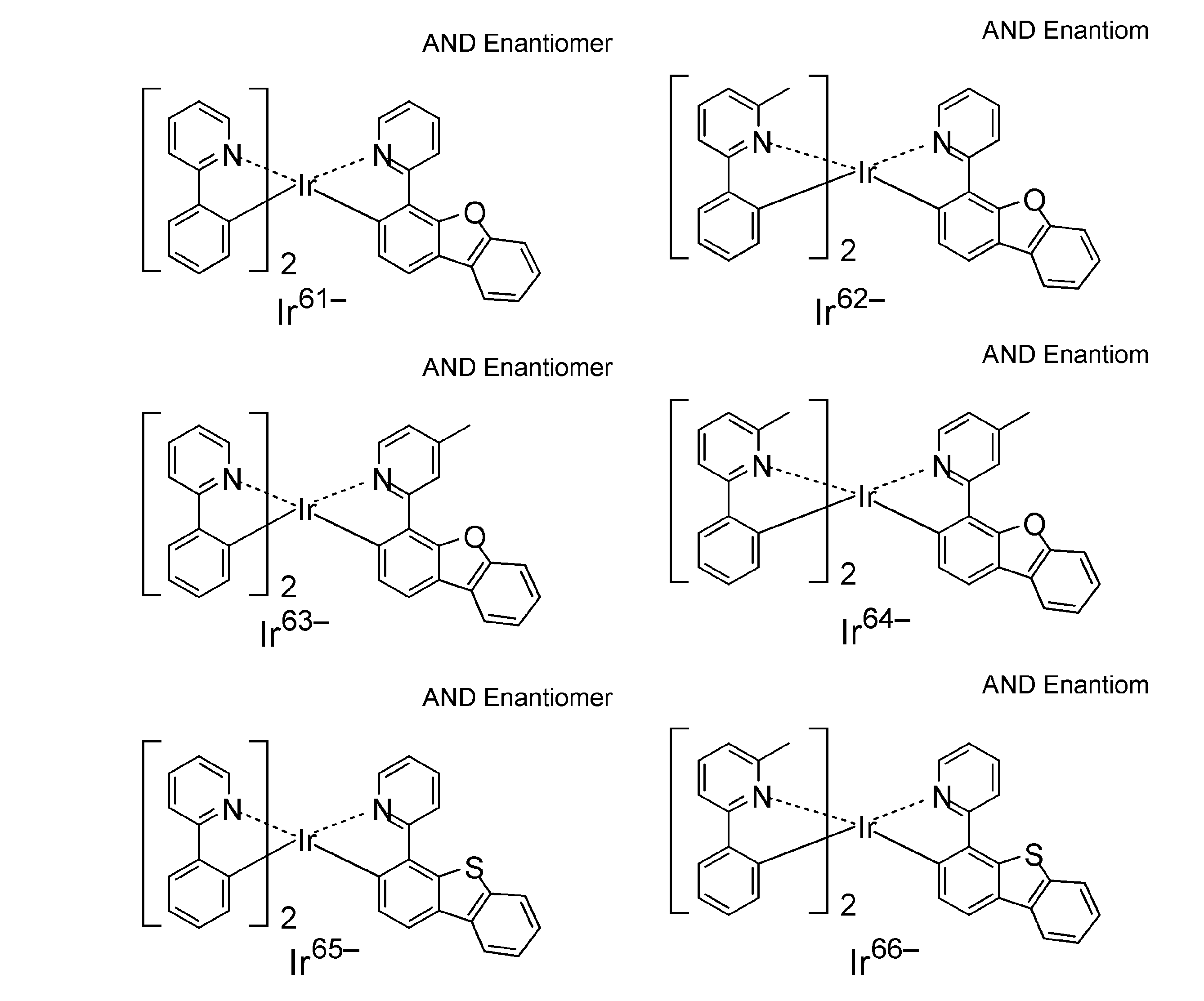

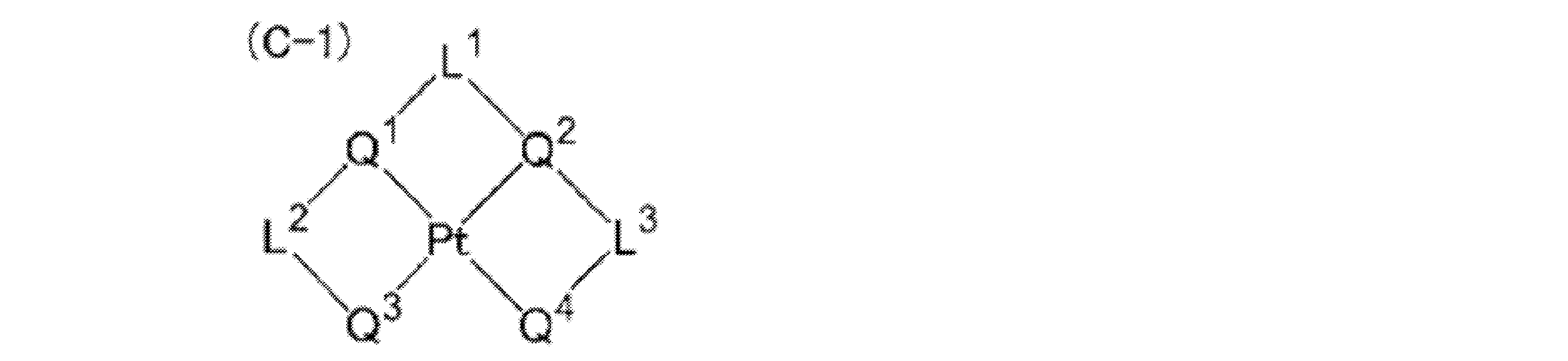
炭素原子で白金(Pt)に結合するQ1、Q2、Q3及びQ4としては、アニオン性の配位子でも中性の配位子でもよく、アニオン性の配位子としてはビニル配位子、芳香族炭化水素環配位子(例えばベンゼン配位子、ナフタレン配位子、アントラセン配位子、フェナントレン配位子など)、ヘテロ環配位子(例えばフラン配位子、チオフェン配位子、ピリジン配位子、ピラジン配位子、ピリミジン配位子、ピリダジン配位子、トリアジン配位子、チアゾール配位子、オキサゾール配位子、ピロール配位子、イミダゾール配位子、ピラゾール配位子、トリアゾール配位子及び、それらを含む縮環体(例えばキノリン配位子、ベンゾチアゾール配位子など))が挙げられる。中性の配位子としてはカルベン配位子が挙げられる。
錯体の安定性及び発光量子収率の観点から、L1、L2及びL3として好ましくは単結合、アルキレン基、アリーレン基、ヘテロアリーレン基、イミノ基、オキシ基、チオ基、シリレン基であり、より好ましくは単結合、アルキレン基、アリーレン基、イミノ基であり、更に好ましくは単結合、アルキレン基、アリーレン基であり、更に好ましくは、単結合、メチレン基、フェニレン基であり、更に好ましくは単結合、ジ置換のメチレン基であり、更に好ましくは単結合、ジメチルメチレン基、ジエチルメチレン基、ジイソブチルメチレン基、ジベンジルメチレン基、エチルメチルメチレン基、メチルプロピルメチレン基、イソブチルメチルメチレン基、ジフェニルメチレン基、メチルフェニルメチレン基、シクロヘキサンジイル基、シクロペンタンジイル基、フルオレンジイル基、フルオロメチルメチレン基である。
L1は特に好ましくはジメチルメチレン基、ジフェニルメチレン基、シクロヘキサンジイル基であり、最も好ましくはジメチルメチレン基である。
L2及びL3として最も好ましくは単結合である。


A401~A414はそれぞれ独立にC-R又は窒素原子を表す。Rは水素原子又は置換基を表す。
Rで表される置換基としては、前記置換基群Aとして挙げたものが適用できる。
A401~A406として好ましくはC-Rであり、R同士が互いに連結して環を形成していても良い。A401~A406がC-Rである場合に、A402、A405のRとして好ましくは水素原子、アルキル基、アリール基、アミノ基、アルコキシ基、アリールオキシ基、フッ素原子、シアノ基であり、より好ましくは水素原子、アミノ基、アルコキシ基、アリールオキシ基、フッ素原子であり、特に好ましくは水素原子、フッ素原子である。A401、A403、A404、A406のRとして好ましくは水素原子、アルキル基、アリール基、アミノ基、アルコキシ基、アリールオキシ基、フッ素原子、シアノ基であり、より好ましくは水素原子、アミノ基、アルコキシ基、アリールオキシ基、フッ素原子であり、特に好ましく水素原子である。
L41は、前記一般式(C-1)中のL1と同義であり、また好ましい範囲も同様である。

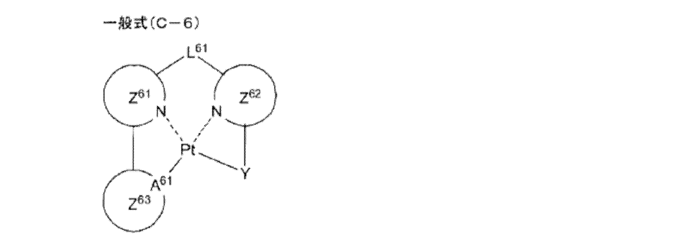
炭素原子で白金(Pt)に結合するYとしてはビニル配位子が挙げられる。窒素原子で白金(Pt)に結合するYとしてはアミノ配位子、イミノ配位子が挙げられる。酸素原子で白金(Pt)に結合するYとしては、アルコキシ配位子、アリールオキシ配位子、ヘテロアリールオキシ配位子、アシルオキシ配位子、シリルオキシ配位子、カルボキシル配位子、リン酸配位子、スルホン酸配位子などが挙げられる。硫黄原子で白金(Pt)に結合するYとしては、アルキルメルカプト配位子、アリールメルカプト配位子、ヘテロアリールメルカプト配位子、チオカルボン酸配位子などが挙げられる。
Yで表される配位子は、置換基を有していてもよく、置換基としては前記置換基群Aとして挙げたものが適宜適用できる。また置換基同士が連結していても良い。


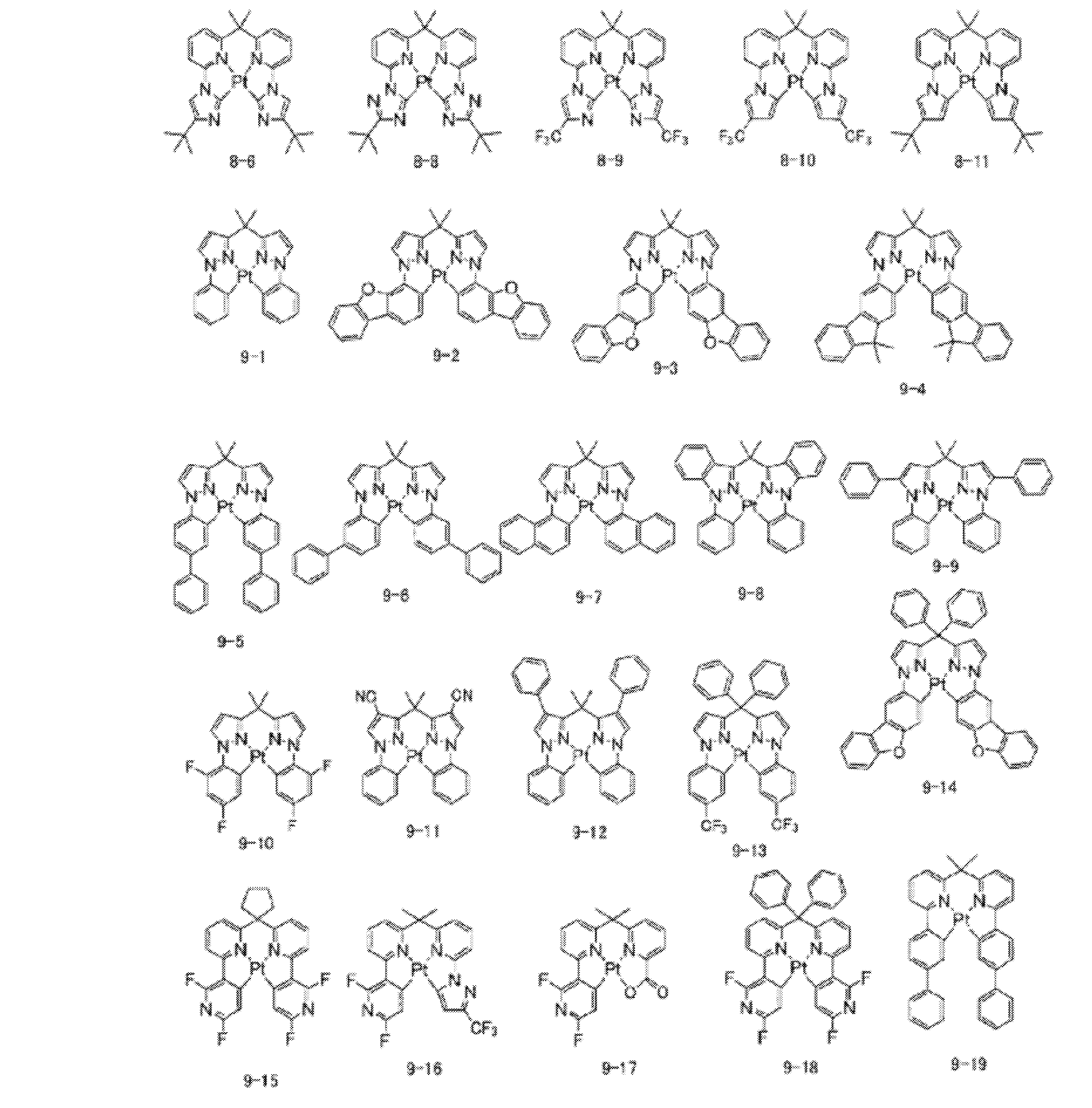
例えば、配位子、又はその解離体と金属化合物を溶媒(例えば、ハロゲン系溶媒、アルコール系溶媒、エーテル系溶媒、エステル系溶媒、ケトン系溶媒、ニトリル系溶媒、アミド系溶媒、スルホン系溶媒、スルホキサイド系溶媒、水などが挙げられる)の存在下、若しくは、溶媒非存在下、塩基の存在下(無機、有機の種々の塩基、例えば、ナトリウムメトキシド、t-ブトキシカリウム、トリエチルアミン、炭酸カリウムなどが挙げられる)、若しくは、塩基非存在下、室温以下、若しくは加熱し(通常の加熱以外にもマイクロウェーブで加熱する手法も有効である)得ることができる。
以下に蛍光発光材料の具体例を示すが、本発明はこれらに限定されるものではない。
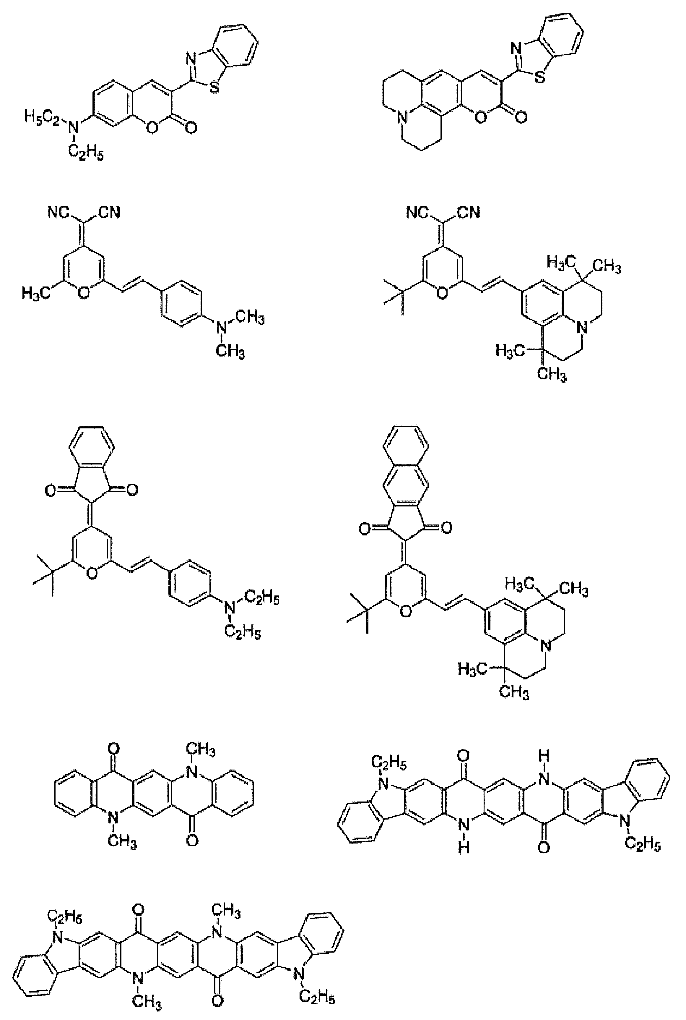

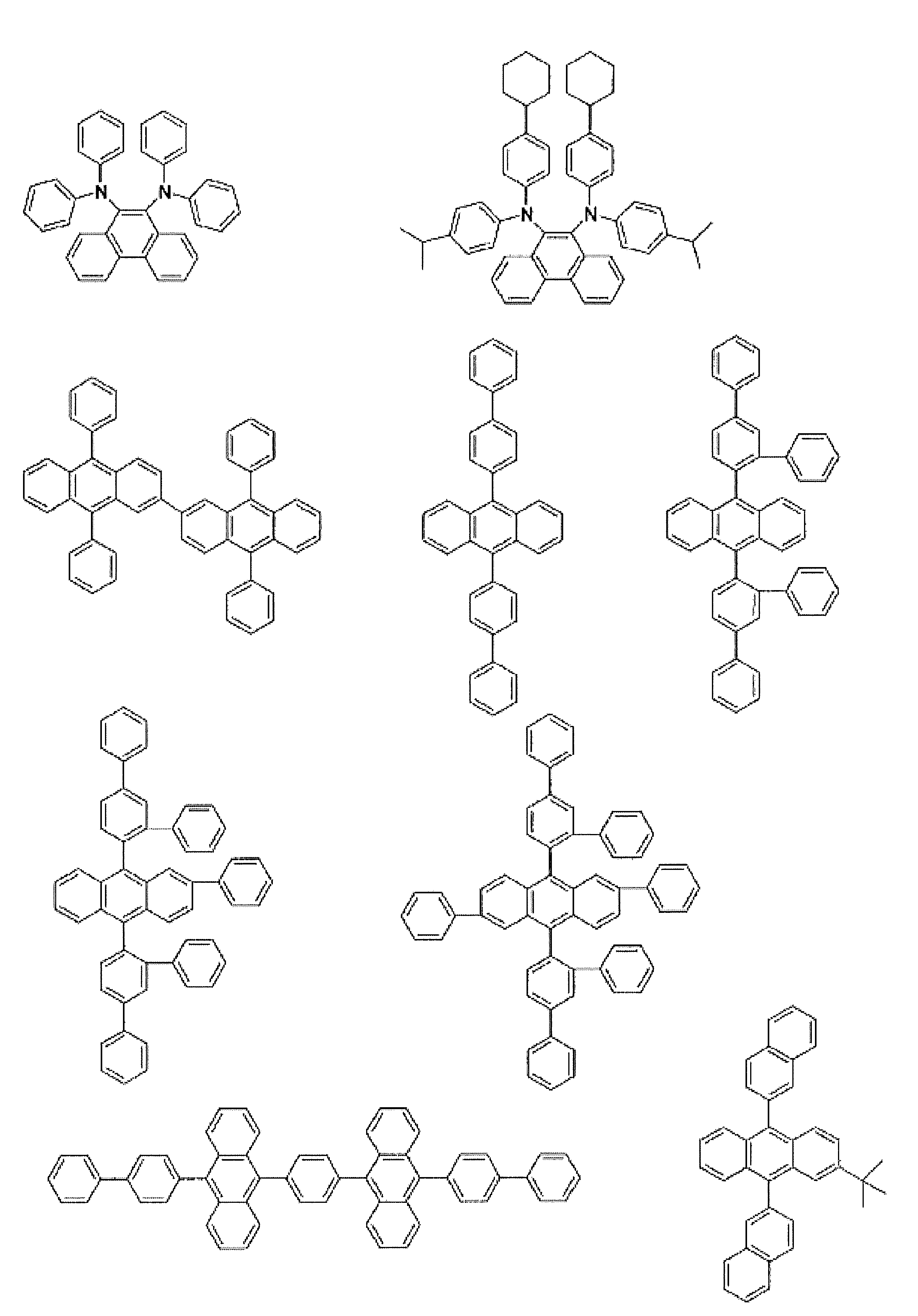
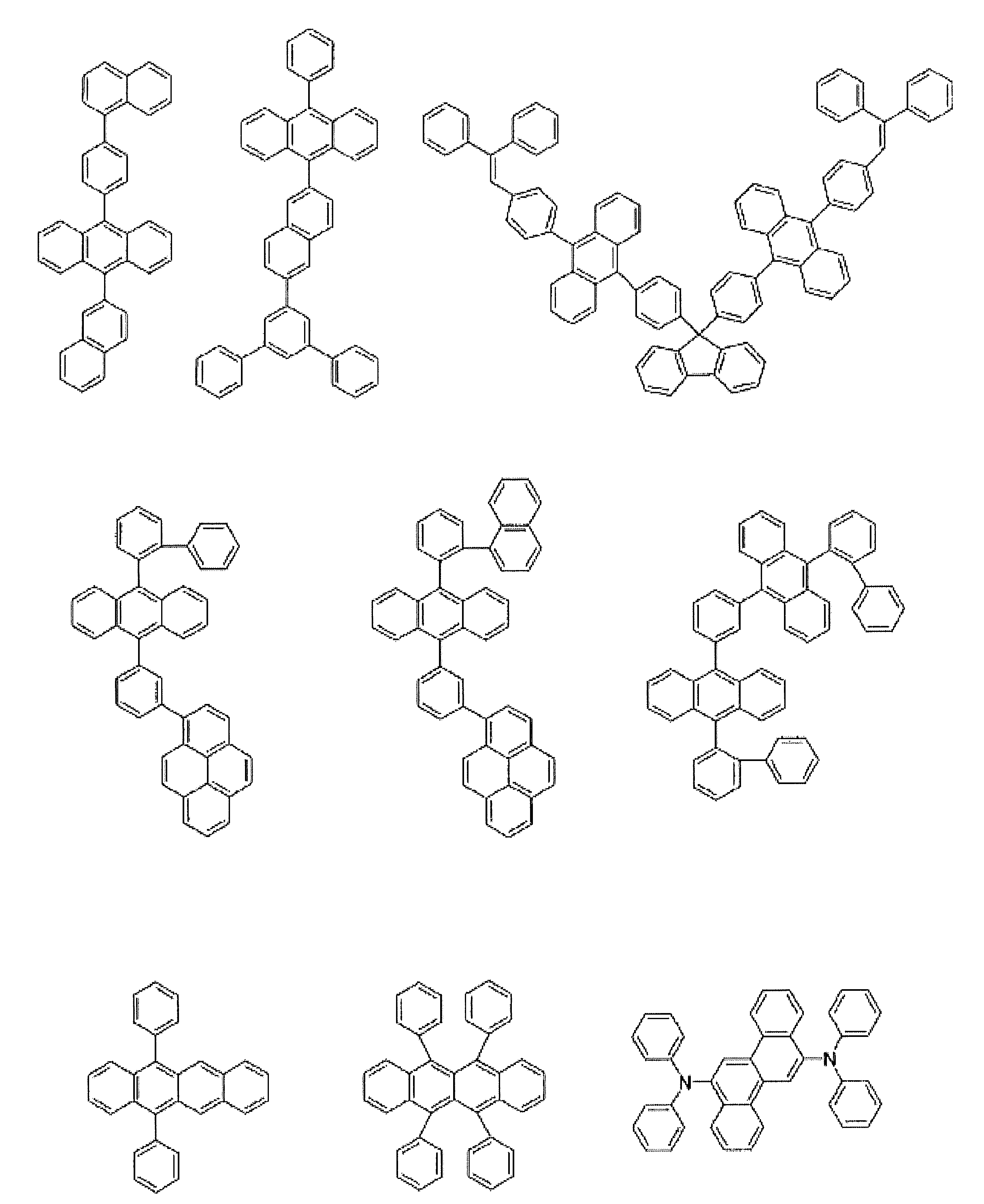


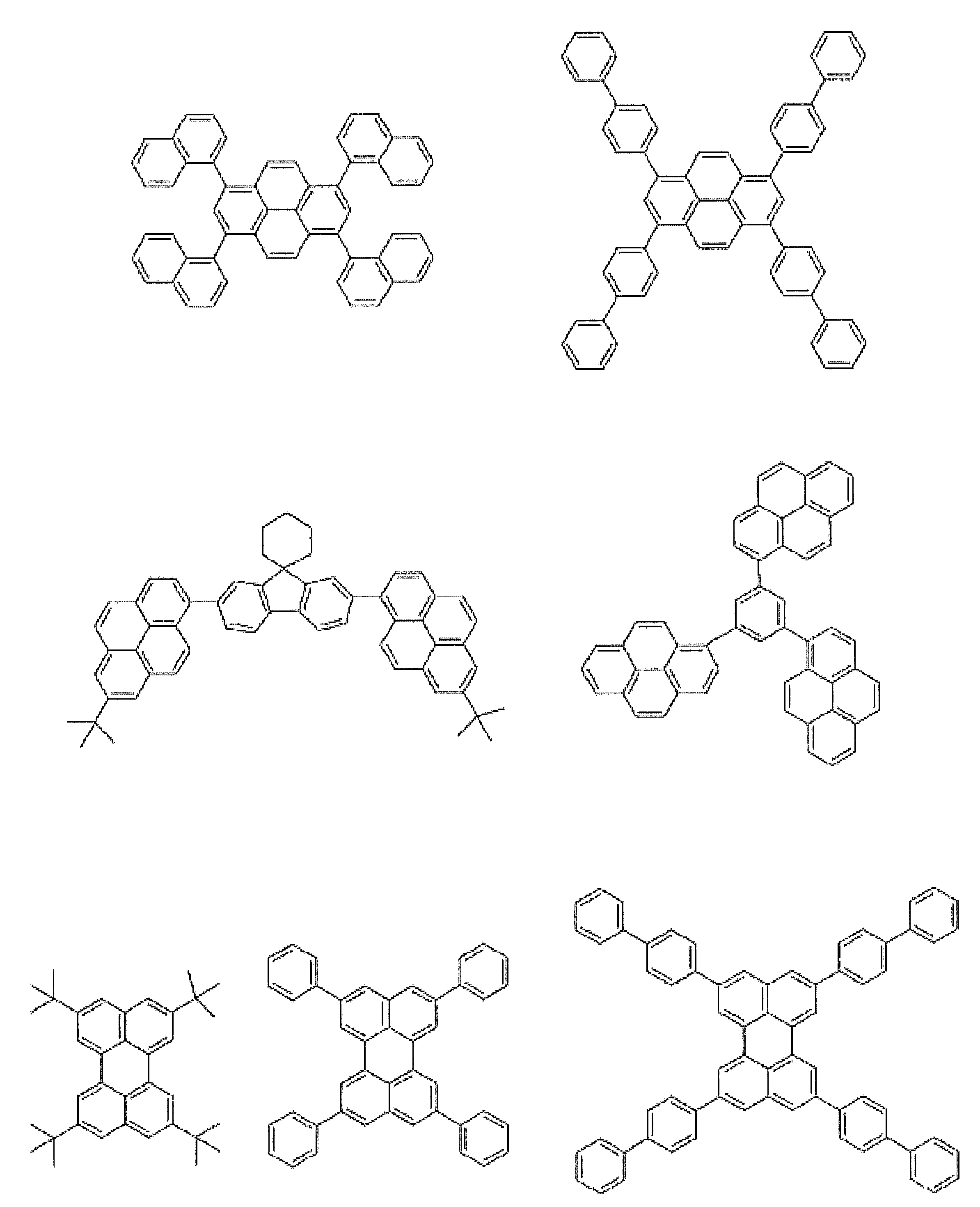
一般式(E-3)で表される燐光発光材料の極大発光波長は、複数のRT1~RT7、及びR'で共同して環形成しない場合にはおよそ500~550nmの範囲、一般式(E-4)又は(E-5)で表される燐光発光材料の極大発光波長は、およそ550~650nmの範囲である。
また、発光層は一層であっても二層以上の多層であってもよく、それぞれの層に同じ発光材料やホスト材料を含んでもよいし、層毎に異なる材料を含んでもよい。発光層が複数の場合、それぞれの発光層が異なる発光色で発光してもよい。
ホスト材料とは、発光層において主に電荷の注入、輸送を担う化合物であり、また、それ自体は実質的に発光しない化合物のことである。ここで「実質的に発光しない」とは、該実質的に発光しない化合物からの発光量が好ましくは素子全体での全発光量の5%以下であり、より好ましくは3%以下であり、更に好ましくは1%以下であることを言う。
ホスト材料としては、一般式(1)で表される化合物を用いることができる。
ピロール、インドール、カルバゾール、アザインドール、アザカルバゾール、トリアゾール、オキサゾール、オキサジアゾール、ピラゾール、イミダゾール、チオフェン、ベンゾチオフェン、ジベンゾチオフェン、フラン、ベンゾフラン、ジベンゾフラン、ポリアリールアルカン、ピラゾリン、ピラゾロン、フェニレンジアミン、アリールアミン、アミノ置換カルコン、スチリルアントラセン、フルオレノン、ヒドラゾン、スチルベン、シラザン、芳香族第三級アミン化合物、スチリルアミン化合物、ポルフィリン系化合物、縮環芳香族炭化水素化合物(アントラセン、ピレン、フルオレン、ナフタレン、フェナントレン、トリフェニレン等)、ポリシラン系化合物、ポリ(N-ビニルカルバゾール)、アニリン系共重合体、チオフェンオリゴマー、ポリチオフェン等の導電性高分子オリゴマー、有機シラン、カーボン膜、ピリジン、ピリミジン、トリアジン、イミダゾール、ピラゾール、トリアゾ-ル、オキサゾ-ル、オキサジアゾ-ル、フルオレノン、アントラキノジメタン、アントロン、ジフェニルキノン、チオピランジオキシド、カルボジイミド、フルオレニリデンメタン、ジスチリルピラジン、フッ素置換芳香族化合物、ナフタレンペリレン等の複素環テトラカルボン酸無水物、フタロシアニン、8-キノリノ-ル誘導体の金属錯体やメタルフタロシアニン、ベンゾオキサゾ-ルやベンゾチアゾ-ルを配位子とする金属錯体に代表される各種金属錯体及びそれらの誘導体(置換基や縮環を有していてもよい)等を挙げることができる。
これらのうち、カルバゾール、ジベンゾチオフェン、ジベンゾフラン、アリールアミン、縮環芳香族炭化水素化合物、金属錯体が特に好ましい。
ホスト材料の膜状態でのT1が燐光発光材料のT1より小さいと発光を消光してしまうためホスト材料には燐光発光材料より大きなT1が求められる。また、ホスト材料のT1が燐光発光材料より大きい場合でも、両者のT1差が小さい場合には一部、燐光発光材料からホスト材料への逆エネルギー移動が起こるため、効率低下や耐久性低下の原因となる。従って、T1が十分に大きく、化学的安定性及びキャリア注入・輸送性の高いホスト材料が求められている。
本発明の有機電界発光素子は、前記発光層以外のその他の層を有していてもよい。
前記有機層が有していてもよい前記発光層以外のその他の有機層として、正孔注入層、正孔輸送層、ブロック層(正孔ブロック層、励起子ブロック層など)、電子輸送層などが挙げられる。前記具体的な層構成として、下記が挙げられるが本発明はこれらの構成に限定されるものではない。
・陽極/正孔輸送層/発光層/電子輸送層/陰極、
・陽極/正孔輸送層/発光層/ブロック層/電子輸送層/陰極、
・陽極/正孔輸送層/発光層/ブロック層/電子輸送層/電子注入層/陰極、
・陽極/正孔注入層/正孔輸送層/発光層/ブロック層/電子輸送層/陰極、
・陽極/正孔注入層/正孔輸送層/発光層/電子輸送層/電子注入層/陰極、
・陽極/正孔注入層/正孔輸送層/発光層/ブロック層/電子輸送層/電子注入層/陰極、
・陽極/正孔注入層/正孔輸送層/ブロック層/発光層/ブロック層/電子輸送層/電子注入層/陰極。
本発明の有機電界発光素子は、(A)前記陽極と前記発光層との間に好ましく配置される有機層を少なくとも一層含むことが好ましい。前記(A)前記陽極と前記発光層との間に好ましく配置される有機層としては、陽極側から正孔注入層、正孔輸送層、電子ブロック層を挙げることができる。
本発明の有機電界発光素子は、(B)前記陰極と前記発光層との間に好ましく配置される有機層少なくとも一層含むことが好ましい。前記(B)前記陰極と前記発光層との間に好ましく配置される有機層としては、陰極側から電子注入層、電子輸送層、正孔ブロック層を挙げることができる。
具体的には、本発明の有機電界発光素子の好ましい態様の一例は、図1に記載される態様であり、前記有機層として、陽極側3から正孔注入層4、正孔輸送層5、発光層6、正孔ブロック層7及び電子輸送層8がこの順に積層されている態様である。
以下、これら本発明の有機電界発光素子が有していてもよい前記発光層以外のその他の層について、説明する。
まず、(A)前記陽極と前記発光層との間に好ましく配置される有機層について説明する。
正孔注入層、正孔輸送層は、陽極又は陽極側から正孔を受け取り陰極側に輸送する機能を有する層である。
正孔注入層、正孔輸送層については、特開2008-270736号公報の段落番号〔0165〕~〔0167〕に記載の事項を本発明に適用することができる。
電子ブロック層は、陰極側から発光層に輸送された電子が、陽極側に通りぬけることを防止する機能を有する層である。本発明において、発光層と陽極側で隣接する有機層として、電子ブロック層を設けることができる。
電子ブロック層を構成する有機化合物の例としては、例えば前述の正孔輸送材料として挙げたものが適用できる。
電子ブロック層の厚さとしては、1nm~500nmであるのが好ましく、3nm~100nmであるのがより好ましく、5nm~50nmであるのが更に好ましい。
電子ブロック層は、上述した材料の一種又は二種以上からなる単層構造であってもよいし、同一組成又は異種組成の複数層からなる多層構造であってもよい。
電子ブロック層に用いる材料は、前記燐光発光材料のT1エネルギーより高いことが色純度、発光効率、駆動耐久性の点で好ましい。電子ブロック層に用いる材料の膜状態でのT1が燐光発光材料のT1より0.1eV以上大きいことが好ましく、0.2eV以上大きいことがより好ましく、0.3eV以上大きいことが更に好ましい。
次に、前記(B)陰極と前記発光層との間に好ましく配置される有機層について説明する。
電子注入層、電子輸送層は、陰極又は陰極側から電子を受け取り陽極側に輸送する機能を有する層である。これらの層に用いる電子注入材料、電子輸送材料は低分子化合物であっても高分子化合物であってもよい。
電子輸送材料としては、前記一般式(1)で表される化合物を用いることができる。その他の電子輸送材料としては、ピリジン誘導体、キノリン誘導体、ピリミジン誘導体、ピラジン誘導体、フタラジン誘導体、フェナントロリン誘導体、トリアジン誘導体、トリアゾール誘導体、オキサゾール誘導体、オキサジアゾール誘導体、イミダゾール誘導体、ベンゾイミダゾール誘導体、イミダゾピリジン誘導体、フルオレノン誘導体、アントラキノジメタン誘導体、アントロン誘導体、ジフェニルキノン誘導体、チオピランジオキシド誘導体、カルボジイミド誘導体、フルオレニリデンメタン誘導体、ジスチリルピラジン誘導体、ナフタレン、ペリレン等の芳香環テトラカルボン酸無水物、フタロシアニン誘導体、8-キノリノール誘導体の金属錯体やメタルフタロシアニン、ベンゾオキサゾールやベンゾチアゾールを配位子とする金属錯体に代表される各種金属錯体、シロールに代表される有機シラン誘導体、ナフタレン、アントラセン、フェナントレン、トリフェニレン、ピレン等の縮環炭化水素化合物等をから選ばれることが好ましく、ピリジン誘導体、ベンゾイミダゾール誘導体、イミダゾピリジン誘導体、金属錯体、縮環炭化水素化合物のいずれかであることがより好ましい。
電子輸送層の厚さとしては、1nm~500nmであるのが好ましく、5nm~200nmであるのがより好ましく、10nm~100nmであるのが更に好ましい。また、電子注入層の厚さとしては、0.1nm~200nmであるのが好ましく、0.2nm~100nmであるのがより好ましく、0.5nm~50nmであるのが更に好ましい。
電子注入層、電子輸送層は、上述した材料の1種又は2種以上からなる単層構造であってもよいし、同一組成又は異種組成の複数層からなる多層構造であってもよい。
正孔ブロック層は、陽極側から発光層に輸送された正孔が、陰極側に通りぬけることを防止する機能を有する層である。本発明において、発光層と陰極側で隣接する有機層として、正孔ブロック層を設けることができる。
正孔ブロック層を構成する有機化合物の膜状態でのT1エネルギーは、発光層で生成する励起子のエネルギー移動を防止し、発光効率を低下させないために、発光材料のT1エネルギーよりも高いことが好ましい。
正孔ブロック層を構成する有機化合物の例としては、前記一般式(1)で表される化合物を用いることができる。
前記一般式(1)で表される化合物以外の、正孔ブロック層を構成するその他の有機化合物の例としては、アルミニウム(III)ビス(2-メチル-8-キノリナト)4-フェニルフェノレート(Aluminum (III)bis(2-methyl-8-quinolinato)4-phenylphenolate(Balqと略記する))等のアルミニウム錯体、トリアゾール誘導体、2,9-ジメチル-4,7-ジフェニル-1,10-フェナントロリン(2,9-Dimethyl-4,7-diphenyl-1,10-phenanthroline(BCPと略記する))等のフェナントロリン誘導体、等が挙げられる。
正孔ブロック層の厚さとしては、1nm~500nmであるのが好ましく、3nm~100nmであるのがより好ましく、5nm~50nmであるのが更に好ましい。
正孔ブロック層は、上述した材料の一種又は二種以上からなる単層構造であってもよいし、同一組成又は異種組成の複数層からなる多層構造であってもよい。
正孔ブロック層に用いる材料は、前記燐光発光材料のT1エネルギーより高いことが色純度、発光効率、駆動耐久性の点で好ましい。正孔ブロック層に用いる材料の膜状態でのT1が燐光発光材料のT1より0.1eV以上大きいことが好ましく、0.2eV以上大きいことがより好ましく、0.3eV以上大きいことが更に好ましい。
本発明の有機電界発光素子は、前記(B)陰極と前記発光層との間に好ましく配置される有機層の材料に特に好ましく用いられる材料として、前記一般式(1)で表される化合物、下記一般式(P-1)で表される化合物および下記一般式(O-1)で表される化合物を挙げることができる。
以下、前記一般式(O-1)で表される化合物と、前記一般式(P-1)で表される化合物について説明する。
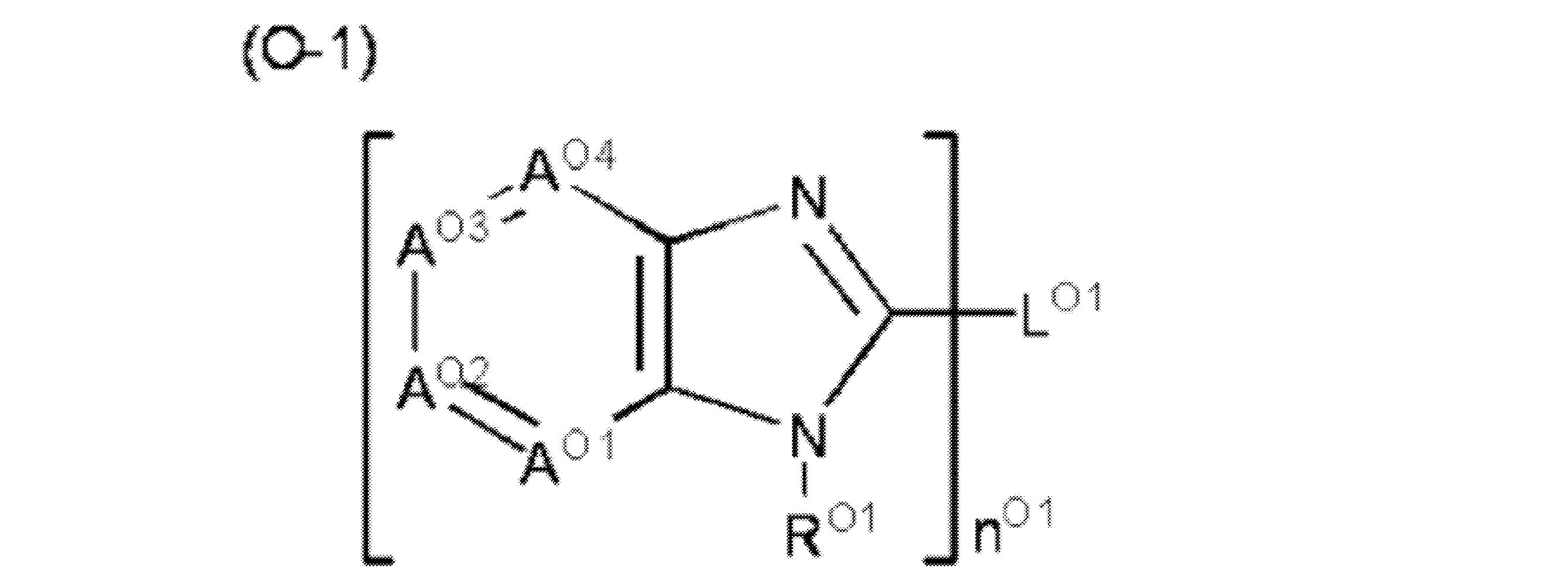

一般式(O-1)で表される化合物は、より好ましくは下記一般式(O-2)で表される化合物である。
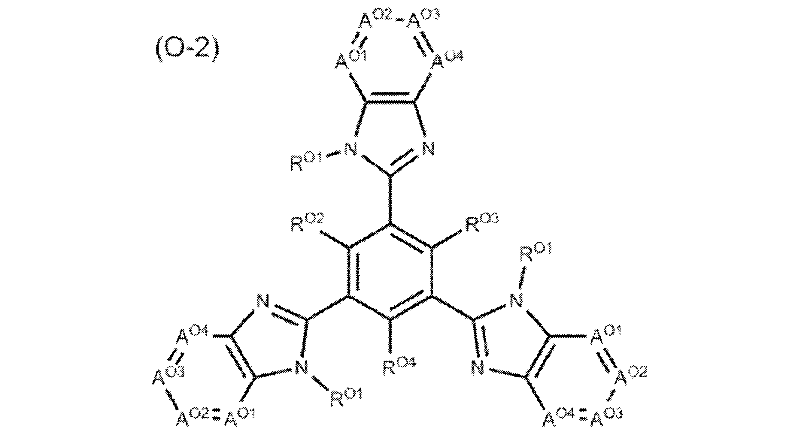
R02~R04はそれぞれ独立に、水素原子、アルキル基(好ましくは炭素数1~8)、アリール基(好ましくは炭素数6~30)、又はヘテロアリール基(好ましくは炭素数4~12)を表し、これらは前述の置換基群Aから選ばれる置換基を有していても良い。R02~R04として好ましくは水素原子、アルキル基、又はアリール基であり、より好ましくは水素原子、又はアリール基であり、最も好ましくは水素原子である。
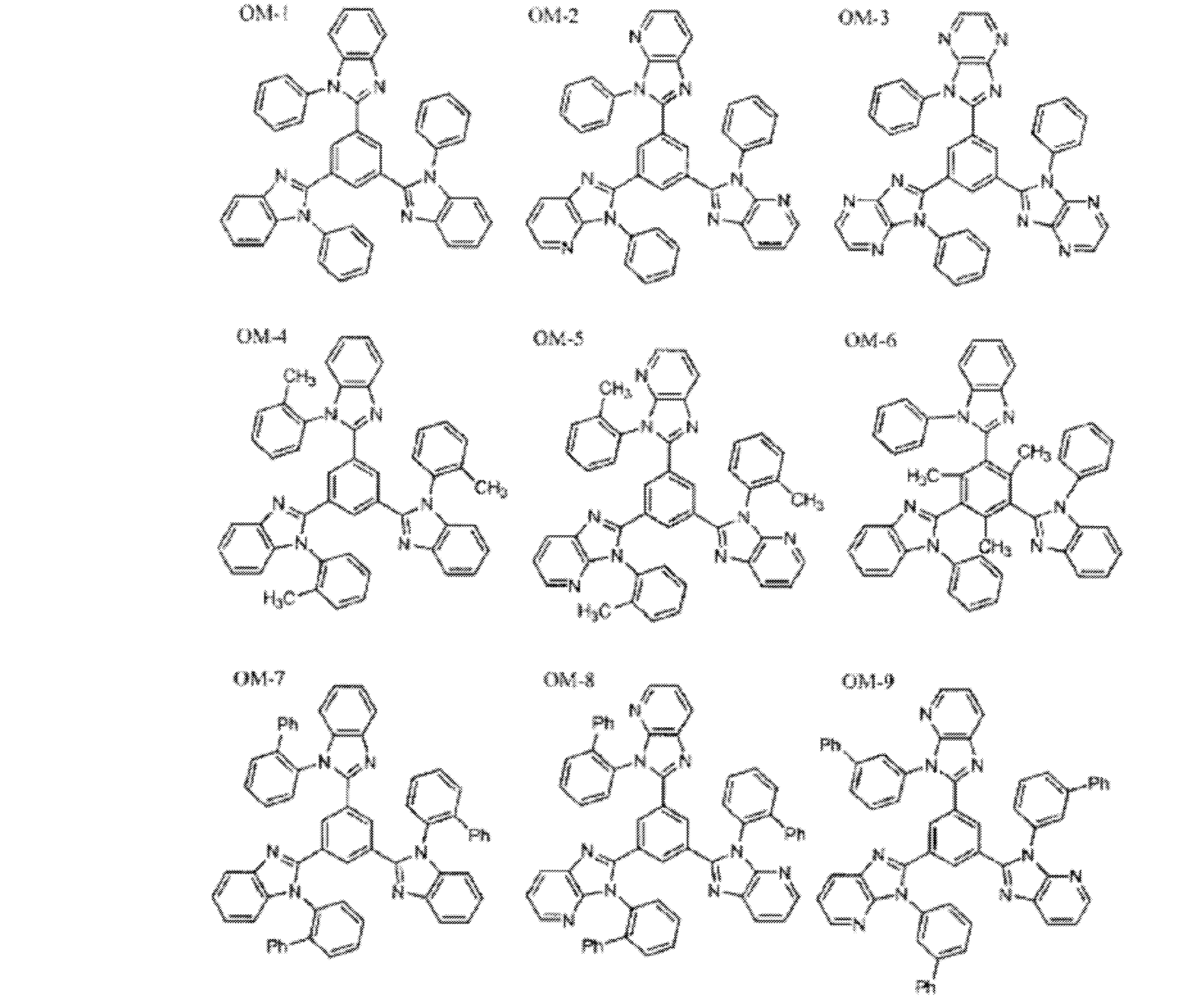
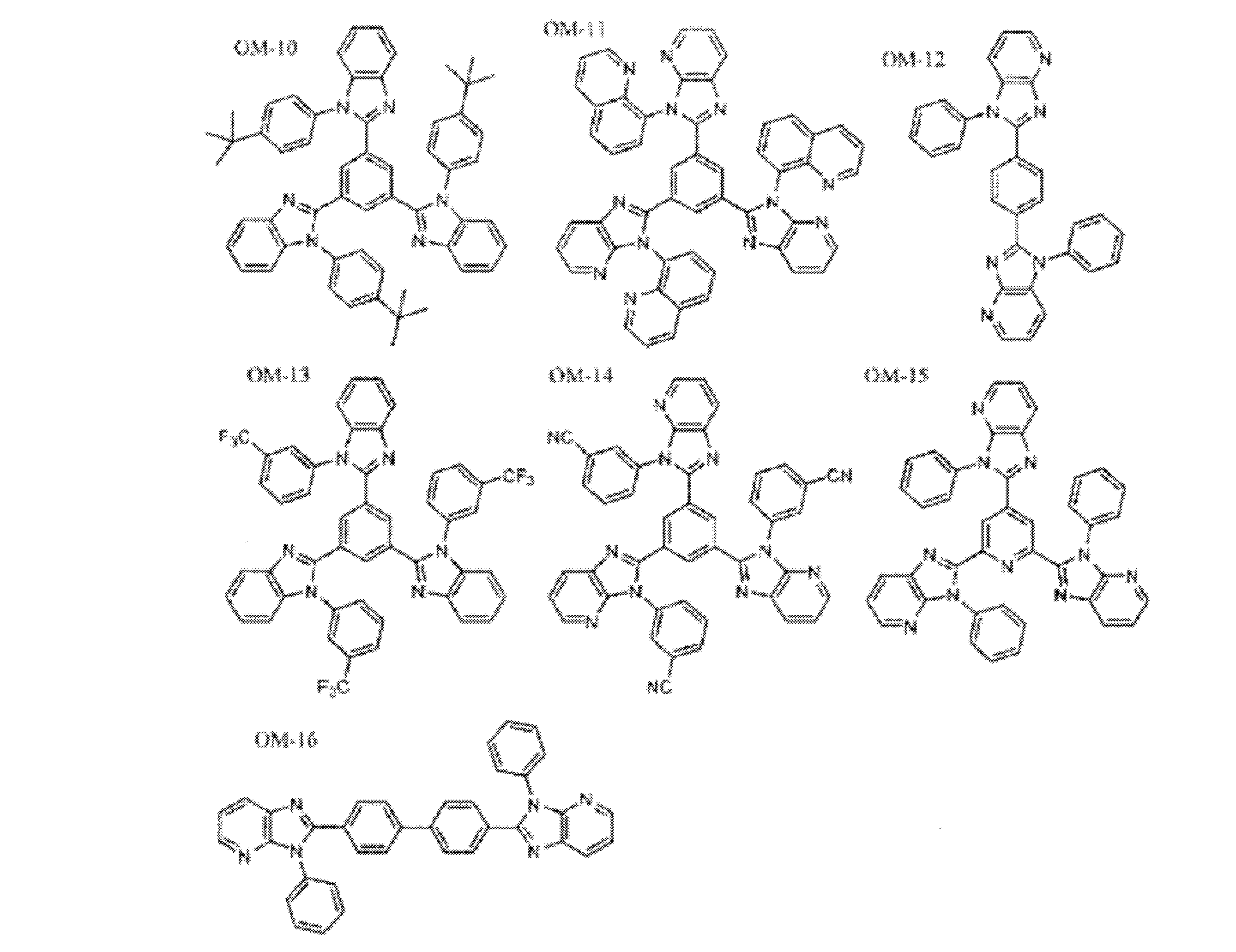
一般式(O-1)で表される化合物は、添加する有機層の全質量に対して70~100質量%含まれることが好ましく、85~100質量%含まれることがより好ましい。


RP1~RP3、R'P1~R'P3として、好ましくはアリール基、ヘテロアリール基のいずれかであり、より好ましくはアリール基であり、更に好ましくはフェニル基、ビフェニル基、ターフェニル基、ナフチル基のいずれかであり、最も好ましくはフェニル基である。
LP1~LP3として、好ましくは単結合、アリール環からなる二価の連結基のいずれかであり、より好ましくは単結合、フェニレン、ビフェニレン、ターフェニレン、ナフチレンのいずれかであり、更に好ましくは単結合、フェニレン、ナフチレンのいずれかである。
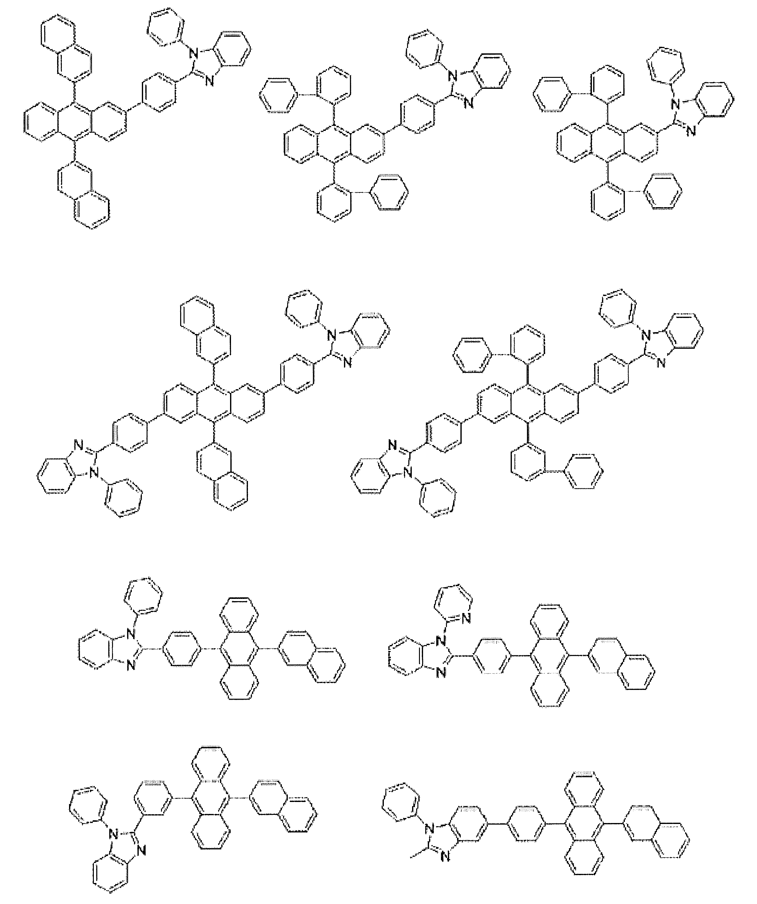

一般式(P)で表される化合物は、添加する有機層の全質量に対して70~100質量%含まれることが好ましく、85~100質量%含まれることがより好ましい。
本発明において、有機電界素子全体は、保護層によって保護されていてもよい。
保護層については、特開2008-270736号公報の段落番号〔0169〕~〔0170〕に記載の事項を本発明に適用することができる。なお、保護層の材料は無機物であっても、有機物であってもよい。
本発明の有機電界発光素子は、封止容器を用いて素子全体を封止してもよい。
封止容器については、特開2008-270736号公報の段落番号〔0171〕に記載の事項を本発明に適用することができる。
本発明の有機電界発光素子は、陽極と陰極との間に直流(必要に応じて交流成分を含んでもよい)電圧(通常2ボルト~15ボルト)、又は直流電流を印加することにより、発光を得ることができる。
本発明の有機電界発光素子の駆動方法については、特開平2-148687号、同6-301355号、同5-29080号、同7-134558号、同8-234685号、同8-241047号の各公報、特許第2784615号、米国特許5828429号、同6023308号の各明細書等に記載の駆動方法を適用することができる。
本発明の有機電界発光素子は、その発光波長に制限はない。例えば、光の三原色のうち、赤色の発光に用いても、緑色の発光に用いても、青色の発光に用いてもよい。その中でも、本発明の有機電界発光素子は、発光波長が500~700nmであることが、前記一般式(1)で表される化合物の最低励起三重項(T1)エネルギーの観点から好ましい。
具体的には、本発明の有機電界発光素子において、前記一般式(1)で表される化合物を発光層のホスト材料として用いる場合は、発光波長が500~700nmであることが好ましく、520~650nmであることがより好ましく、520~550nmであることが特に好ましい。
一方、本発明の有機電界発光素子において、前記一般式(1)で表される化合物を正孔ブロック層の電荷輸送材料として用いる場合は、発光波長が400~700nmであることが好ましく、450~650nmであることがより好ましく、500~650nmであることが特に好ましい。
本発明の有機電界発光素子は、表示素子、ディスプレイ、バックライト、電子写真、照明光源、記録光源、露光光源、読み取り光源、標識、看板、インテリア、又は光通信等に好適に利用できる。特に、発光装置、照明装置、表示装置等の発光輝度が高い領域で駆動されるデバイスに好ましく用いられる。
本発明の発光装置は、本発明の有機電界発光素子を含むことを特徴とする。
次に、図2を参照して本発明の発光装置について説明する。
本発明の発光装置は、前記有機電界発光素子を用いてなる。
図2は、本発明の発光装置の一例を概略的に示した断面図である。図2の発光装置20は、透明基板(支持基板)2、有機電界発光素子10、封止容器16等により構成されている。
ここで、接着層14としては、エポキシ樹脂等の光硬化型接着剤や熱硬化型接着剤を用いることができ、例えば熱硬化性の接着シートを用いることもできる。
本発明の照明装置は、本発明の有機電界発光素子を含むことを特徴とする。
次に、図3を参照して本発明の照明装置について説明する。
図3は、本発明の照明装置の一例を概略的に示した断面図である。本発明の照明装置40は、図3に示すように、前述した有機EL素子10と、光散乱部材30とを備えている。より具体的には、照明装置40は、有機EL素子10の基板2と光散乱部材30とが接触するように構成されている。
光散乱部材30は、光を散乱できるものであれば特に制限されないが、図3においては、透明基板31に微粒子32が分散した部材とされている。透明基板31としては、例えば、ガラス基板を好適に挙げることができる。微粒子32としては、透明樹脂微粒子を好適に挙げることができる。ガラス基板及び透明樹脂微粒子としては、いずれも、公知のものを使用できる。このような照明装置40は、有機電界発光素子10からの発光が散乱部材30の光入射面30Aに入射されると、入射光を光散乱部材30により散乱させ、散乱光を光出射面30Bから照明光として出射するものである。
本発明の表示装置は、本発明の有機電界発光素子を含むことを特徴とする。 本発明の表示装置としては、例えば、テレビ、パーソナルコンピュータ、携帯電話、電子ペーパ等の表示装置とすることなどを挙げることができる。
前記一般式(1)で表される化合物は、特表2010-535809に記載の方法や、その他公知の反応を組み合わせて合成できる。
(合成例1)化合物2の合成
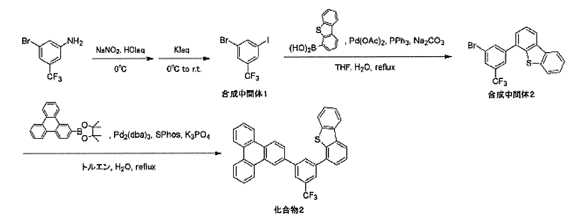
合成中間体1を5.00g(14.2mmol)、ジベンゾチオフェン-4-ボロン酸3.24g(14.2mmol)、酢酸パラジウム0.16g(0.71mmol)、トリフェニルホスフィン0.75g(2.84mmol)、4.52g(42.6mmol)、脱水テトラヒドロフランを混合し、窒素雰囲気下、6.5時間加熱還流した。反応液を室温に戻した後、トルエンを加えて分液し、有機層をシリカゲルカラムクロマトグラフィー(展開溶媒:トルエン)により精製した。その後、メタノール、ヘキサンで順次たき洗いすることにより、合成中間体2を2.80g得た(収率48%)。
合成中間体2を1.40g(3.44mmol)、4,4,5,5-テトラメチル-2-(トリフェニレン-2-イル)-1,3,2-ジオキサボラン1.46g(4.13mmol)、トリス(ジベンジリデンアセトン)ジパラジウム(Pd2(dba)3)0.094g(0.10mmol)、2-ジシクロヘキシルホスフィノ-2',6'-ジメトキシビフェニル(SPhos)0.17g(0.41mmol)、リン酸カリウム2.92g(13.8mmol)、トルエン10mL、水10mLを混合し、窒素雰囲気下、5時間加熱還流した。反応液を室温に戻し、析出した固体を濾過した。得られた固体をTHFで加熱還流して完溶後、トルエン20mLを添加し、加熱還流下THFを留去し、室温に戻した。析出した固体を濾過し、トルエンで洗浄することで化合物2を1.30g得た(収率68%)。
化合物2のNMRデータ
1H NMR(400MHz,in DMSO-d6);δ(ppm)=9.27(s,1H),9.15-9.12(m,1H),8.98(d,1H),8.91-8.84(m,3H),8.66(s,1H),8.53-8.44(m,3H),8.25-8.22(m,1H),8.15(s,1H),8.09-8.07(m,1H),7.88(d,1H),7.77-7.72(m,5H),7.60-7.54(m,2H)ppm.
化合物1、化合物3~10も化合物2の合成法に準じて合成した。
素子作製に用いた材料は全て昇華精製を行い、高速液体クロマトグラフィー(東ソーTSKgel ODS-100Z)により純度(254nmの吸収強度面積比)が99.9%以上であることを確認した。なお、比較化合物1および比較化合物2は、それぞれ特表2010-535809に記載の化合物2Sおよび2Oであり、比較化合物3は国際公開WO2009/074087号公報に記載の化合物3-45である。
厚み0.5mm、2.5cm角のITO膜を有するガラス基板(ジオマテック社製、表面抵抗10Ω/□)を洗浄容器に入れ、2-プロパノール中で超音波洗浄した後、30分間UV-オゾン処理を行った。この透明陽極(ITO膜)上に真空蒸着法にて以下の有機化合物層を順次蒸着した。
第1層:HAT-CN:膜厚10nm
第2層:NPD:膜厚30nm
第3層:表1中に記載のホスト材料及びGD-1(質量比90:10):膜厚30nm
第4層:表1中に記載のHBL材料:膜厚5nm
第5層:Alq:膜厚45nm
この上に、フッ化リチウム0.1nm及び金属アルミニウム100nmをこの順に蒸着し陰極とした。
得られた積層体を、大気に触れさせることなく、窒素ガスで置換したグローブボックス内に入れ、ガラス製の封止缶及び紫外線硬化型の接着剤(XNR5516HV、長瀬チバ(株)製)を用いて封止し、素子1-1~1-7、比較素子1-1~1-5を得た。発光部分は2mm×2mmの正方形である。これらの素子を以下の方法で効率、駆動電圧、耐久性、高温保管後の効率の観点で評価した結果を表1に示す。
各素子を105℃の恒温槽中で100時間保管後、東陽テクニカ製ソースメジャーユニット2400を用いて、直流電圧を各素子に印加し発光させ、その輝度をトプコン社製輝度計BM-8を用いて測定した。これらを元に輝度が1000cd/m2付近の外部量子効率(η)を輝度換算法により算出した。表1においては比較素子1-1の値を、表2においては比較素子2-1の値を、表3においては比較素子3-1の値を、表4においては比較素子4-1の値を、表5においては比較素子5-1の値を、表6においては比較素子6-1の値をそれぞれ1.0として、各表において相対値で示した。効率は数字が大きいほど好ましい。
各素子を105℃の恒温槽中で100時間保管後、輝度が5000cd/m2になるように直流電圧を印加して発光させ続け、輝度が4000cd/m2になるまでに要した時間を耐久性の指標とした。表1においては比較素子1-1の値を、表2においては比較素子2-1の値を、表3においては比較素子3-1の値を、表4においては比較素子4-1の値を、表5においては比較素子5-1の値を、表6においては比較素子6-1の値をそれぞれ1.0として、各表において相対値で示した。耐久性は数字が大きいほど好ましい。
同一条件で10個の素子を作製し、顕微鏡下で各素子を4000cd/m2の輝度で発光させながら発光表面を観察したとき、6個以上の素子でダークスポットの存在が確認された場合は××、2~5個の素子でダークスポットの存在が確認された場合は×、ダークスポットの存在が確認されたものが1個以下の場合は○と記載した。

一方、比較例1、2の有機電界発光素子は、発光層のホスト化合物として比較化合物1、2を用いたものであり、高温保管後の効率、駆動耐久性が悪く、ダークスポットの発生が顕著であった。また、比較化合物3を用いた比較素子1-3では、発光材料GD-1の発光が確認できなかった。
なお、実施例1で作製した有機電界発光素子の発光波長は522~528nmであった。
層構成を以下に示すものに変えた以外は実施例1と同様にして素子を作製し、実施例1と同様の評価を行った結果を表2に示す。
第1層:2-TNATA及びF4-TCNQ(質量比99.7:0.3) :膜厚160nm
第2層:NPD:膜厚5nm
第3層:HT-1:膜厚3nm
第4層:H-1及びGD-2(質量比85:15):膜厚30nm
第5層:表2中に記載のHBL材料:膜厚10nm
第6層:ET-2:膜厚20nm
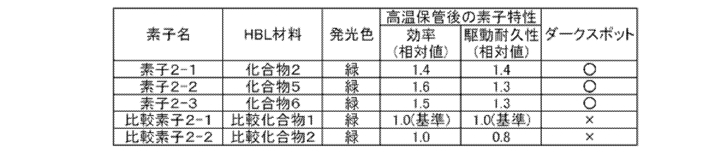
一方、比較例1、2の有機電界発光素子は、正孔ブロック層の材料として比較化合物1、2を用いたものであり、高温保管後の効率、駆動耐久性が悪く、ダークスポットの発生が顕著であった。
なお、実施例2で作製した有機電界発光素子の発光波長は503~507nmであった。
層構成を以下に示すものに変えた以外は実施例1と同様にして素子を作製し、実施例1と同様の評価を行った結果を表3に示す。
第1層:CuPc:膜厚10nm
第2層:NPD:膜厚30nm
第3層:表3中に記載のホスト材料及びRD-1(質量比95:5):膜厚30nm
第4層:ET-2:膜厚5nm
第5層:ET-3:膜厚50nm

一方、比較例1、2の有機電界発光素子は、発光層のホスト化合物として比較化合物1、2を用いたものであり、高温保管後の効率、駆動耐久性が悪く、ダークスポットの発生が顕著であった。
なお、実施例3で作製した有機電界発光素子の発光波長は618~622nmであった。
層構成を以下に示すものに変えた以外は実施例1と同様にして素子を作製し、実施例1と同様の評価を行った結果を表4に示す。
第1層:TCTA:膜厚35nm
第2層:HT-2:膜厚5nm
第3層:BAlq及びRD-2(質量比90:10):膜厚30nm
第4層:表4中に記載のHBL材料:膜厚5nm
第5層:ET-4:膜厚45nm
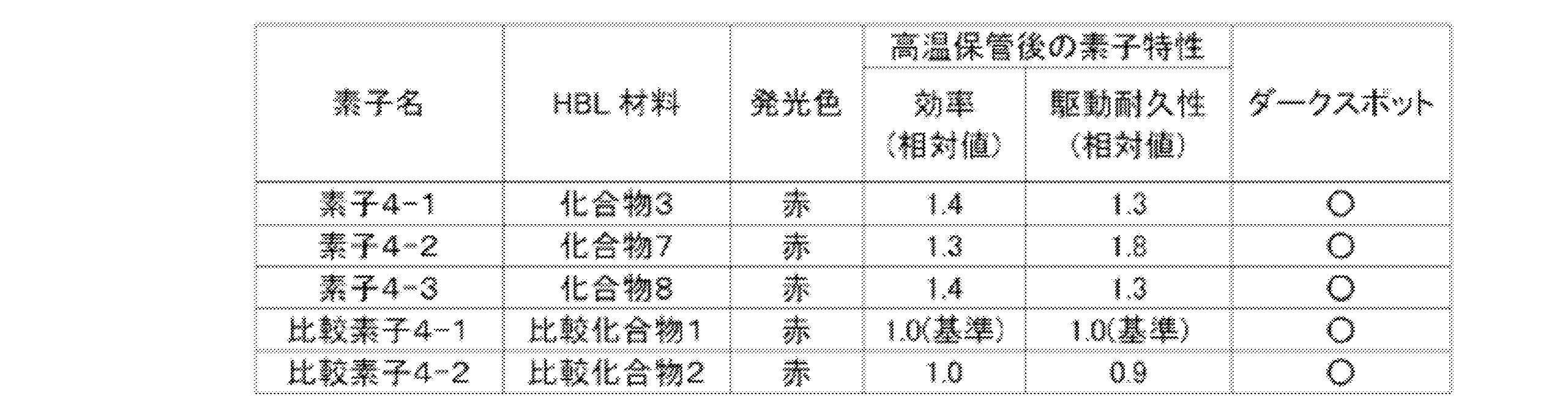
一方、比較例1、2の有機電界発光素子は、正孔ブロック層の材料として比較化合物1、2を用いたものであり、高温保管後の効率、駆動耐久性が悪かった。
なお、実施例4で作製した有機電界発光素子の発光波長は625~629nmであった。
層構成を以下に示すものに変えた以外は実施例1と同様にして素子を作製し、実施例1と同様の評価を行った結果を表5に示す。
第1層:HAT-CN:膜厚10nm
第2層:NPD:膜厚115nm
第3層:HT-3:膜厚5nm
第4層:H-2及びFirpic(質量比90:10):膜厚30nm
第5層:表5中に記載のHBL材料:膜厚5nm
第6層:ET-5:膜厚25nm
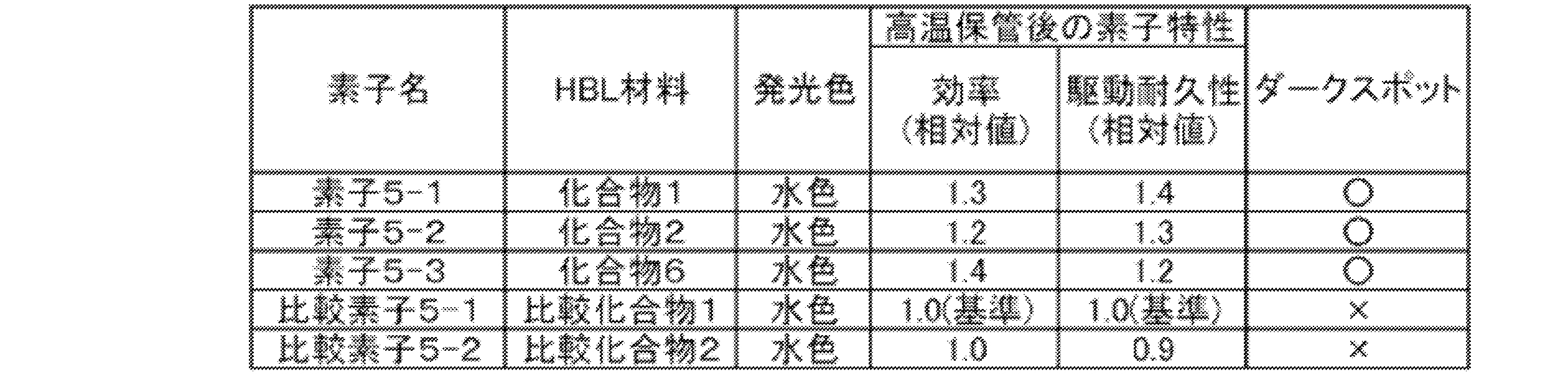
なお、実施例5で作製した有機電界発光素子の発光波長は472~476nmであった。
層構成を以下に示すものに変えた以外は実施例1と同様にして素子を作製し、実施例1と同様の評価を行った結果を表6に示す。
第1層:2-TNATA及びF4-TCNQ(質量比99.7:0.3) :膜厚120nm
第2層:NPD:膜厚7nm
第3層:HT-3:膜厚3nm
第4層:H-3及びBD-1(質量比85:15):膜厚30nm
第5層:表6中に記載のHBL材料:膜厚5nm
第6層:BAlq:膜厚25nm
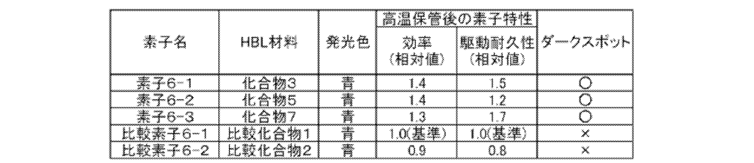
一方、比較例1、2の有機電界発光素子は、正孔ブロック層の材料として比較化合物1、2を用いたものであり、高温保管後の効率、駆動耐久性が悪く、ダークスポットの発生が認められた。
なお、実施例6で作製した有機電界発光素子の発光波長は455~460nmであった。
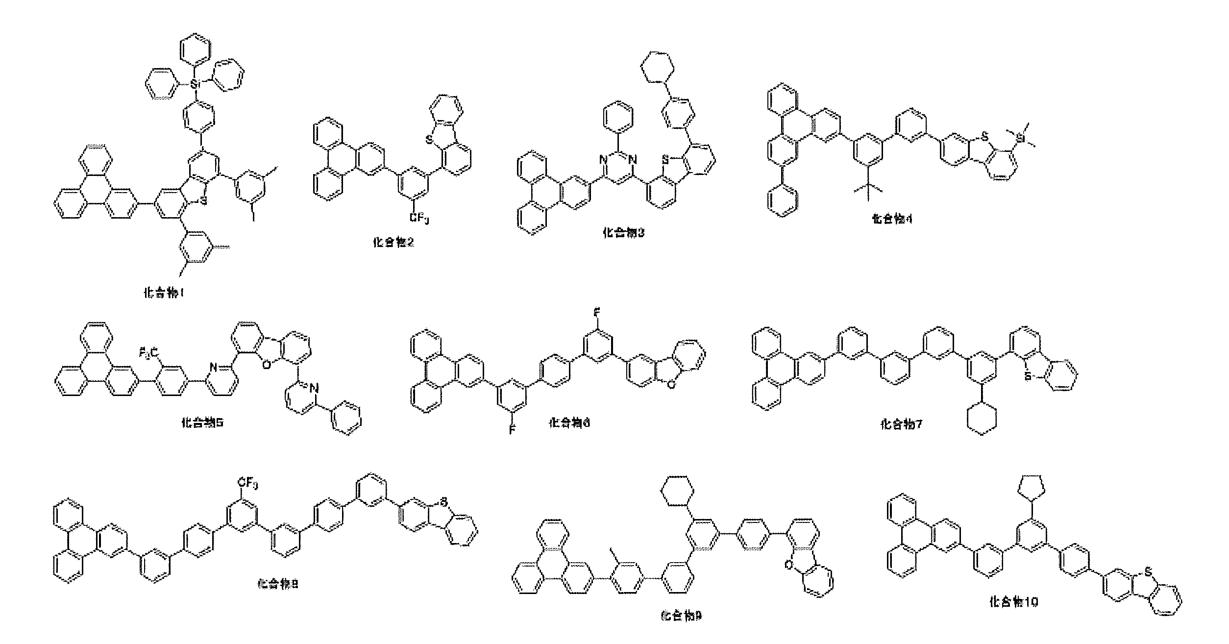
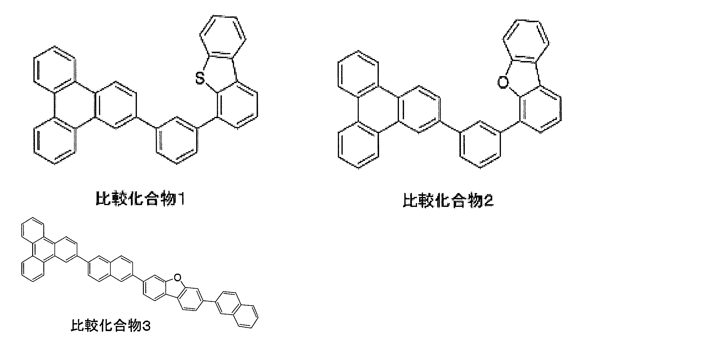

3・・・陽極
4・・・正孔注入層
5・・・正孔輸送層
6・・・発光層
7・・・正孔ブロック層
8・・・電子輸送層
9・・・陰極
10・・・有機電界発光素子
11・・・有機層
12・・・保護層
14・・・接着層
16・・・封止容器
20・・・発光装置
30・・・光散乱部材
31・・・透明基板
30A・・・光入射面
30B・・・光出射面
32・・・微粒子
40・・・照明装置
Claims (16)
- 下記一般式(1)で表される化合物からなることを特徴とする電荷輸送材料。

- 前記一般式(1)で表される化合物が、下記一般式(2)で表されることを特徴とする請求項1に記載の電荷輸送材料。

- 前記一般式(2)におけるm111が1~5であることを特徴とする請求項2に記載の電荷輸送材料。
- 前記一般式(1)で表される化合物が、下記一般式(3)で表されることを特徴とする請求項1~3のいずれか一項に記載の電荷輸送材料。
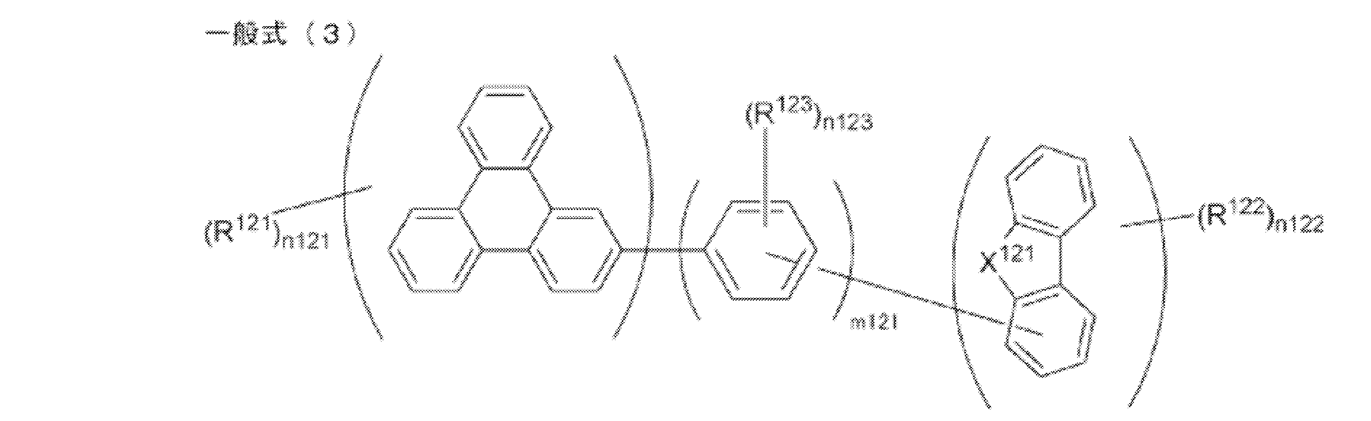
- 前記一般式(1)におけるn101が0であることを特徴とする請求項1~4のいずれか一項に記載の電荷輸送材料。
- 前記一般式(1)におけるn102が0~2の整数である、請求項1~5のいずれか一項に記載の電荷輸送材料。
- 前記一般式(1)で表される化合物が、ジベンゾチオフェン骨格およびジベンゾフラン骨格中の酸素原子および硫黄原子を除き、炭素原子および水素原子のみからなることを特徴とする請求項1~6のいずれか一項に記載の電荷輸送材料。
- 前記一般式(1)で表される化合物が、シクロアルキル基を含むことを特徴とする請求項1~7のいずれか一項に記載の電荷輸送材料。
- 一般式(1)で表される化合物の分子量が1200以下であることを特徴とする請求項1~8のいずれか一項に記載の電荷輸送材料。
- 基板と、
該基板上に配置され、陽極及び陰極を含む一対の電極と、
該電極間に配置された有機層とを有し、
前記有機層が、燐光発光材料と請求項1~9のいずれか一項に記載の電荷輸送材料を含有することを特徴とする有機電界発光素子。 - 前記燐光発光材料が下記一般式(E-1)で表されることを特徴とする請求項10に記載の有機電界発光素子。
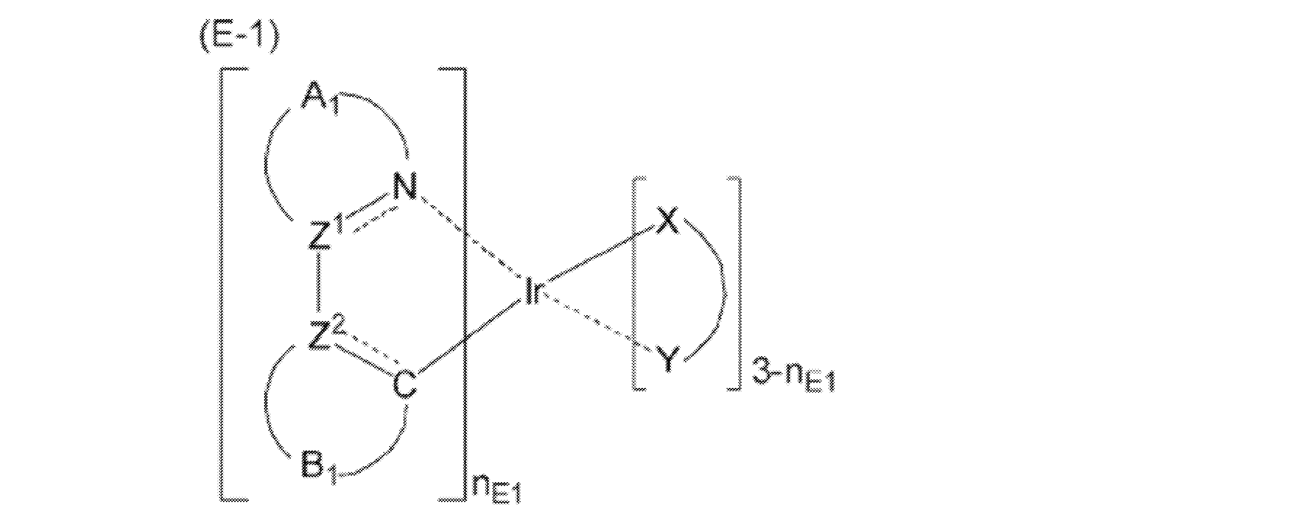
- 前記一般式(E-1)で表される燐光発光材料が下記一般式(E-2)で表されることを特徴とする請求項11に記載の有機電界発光素子。
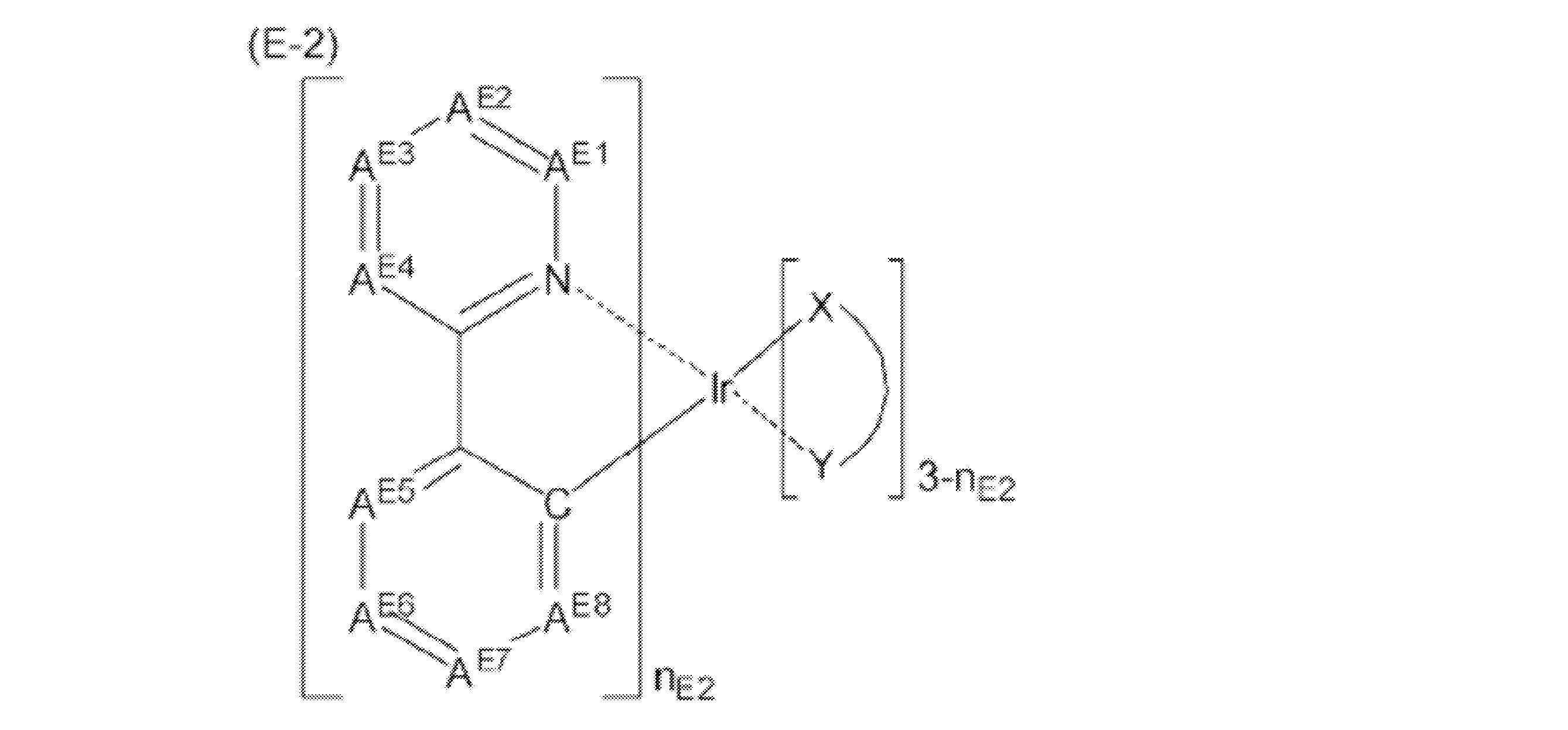
- 前記一般式(E-1)で表される燐光発光材料の極大発光波長が500nm~700nmであることを特徴とする請求項11または12に記載の有機電界発光素子。
- 前記有機層が、前記燐光発光材料を含む発光層とその他の有機層を有し、
前記発光層が前記一般式(1)で表される化合物を含有することを特徴とする請求項10~13のいずれか一項に記載の有機電界発光素子。 - 前記有機層が、前記燐光発光材料を含む発光層とその他の有機層を有し、
該その他の有機層が、前記発光層と前記陰極との間に配置されたホールブロック層を含み、且つ、該ホールブロック層が前記一般式(1)で表される化合物を含有することを特徴とする請求項10~14のいずれか一項に記載の有機電界発光素子。 - 請求項10~15のいずれか一項に記載の有機電界発光素子を用いたことを特徴とする発光装置、表示装置または照明装置。
Priority Applications (2)
| Application Number | Priority Date | Filing Date | Title |
|---|---|---|---|
| KR1020137025081A KR101900979B1 (ko) | 2011-03-31 | 2012-03-29 | 전하 수송 재료, 유기 전계 발광 소자 및 그 소자를 사용한 것을 특징으로 하는 발광 장치, 표시 장치 또는 조명 장치 |
| US14/008,347 US10804469B2 (en) | 2011-03-31 | 2012-03-29 | Charge transport material, organic electroluminescent element, and illumination device, display device, or light-emitting device characterized by using said element |
Applications Claiming Priority (4)
| Application Number | Priority Date | Filing Date | Title |
|---|---|---|---|
| JP2011-080216 | 2011-03-31 | ||
| JP2011080216 | 2011-03-31 | ||
| JP2012072477A JP5973762B2 (ja) | 2011-03-31 | 2012-03-27 | 電荷輸送材料、有機電界発光素子及び該素子を用いたことを特徴とする発光装置、表示装置または照明装置 |
| JP2012-072477 | 2012-03-27 |
Publications (1)
| Publication Number | Publication Date |
|---|---|
| WO2012133653A1 true WO2012133653A1 (ja) | 2012-10-04 |
Family
ID=46931355
Family Applications (1)
| Application Number | Title | Priority Date | Filing Date |
|---|---|---|---|
| PCT/JP2012/058362 Ceased WO2012133653A1 (ja) | 2011-03-31 | 2012-03-29 | 電荷輸送材料、有機電界発光素子及び該素子を用いたことを特徴とする発光装置、表示装置または照明装置 |
Country Status (4)
| Country | Link |
|---|---|
| US (1) | US10804469B2 (ja) |
| JP (1) | JP5973762B2 (ja) |
| KR (1) | KR101900979B1 (ja) |
| WO (1) | WO2012133653A1 (ja) |
Cited By (3)
| Publication number | Priority date | Publication date | Assignee | Title |
|---|---|---|---|---|
| US20160126475A1 (en) * | 2014-11-05 | 2016-05-05 | Samsung Display Co., Ltd. | Organic light-emitting device |
| CN108084081A (zh) * | 2016-11-14 | 2018-05-29 | 环球展览公司 | 有机电致发光材料和装置 |
| WO2023238629A1 (ja) * | 2022-06-06 | 2023-12-14 | キヤノン株式会社 | 有機化合物および有機発光素子 |
Families Citing this family (5)
| Publication number | Priority date | Publication date | Assignee | Title |
|---|---|---|---|---|
| JP5847420B2 (ja) * | 2010-09-08 | 2016-01-20 | ユー・ディー・シー アイルランド リミテッド | 有機電界発光素子及び化合物 |
| JP6350518B2 (ja) * | 2013-03-29 | 2018-07-04 | コニカミノルタ株式会社 | 有機エレクトロルミネッセンス素子、それを具備した照明装置及び表示装置 |
| KR102291487B1 (ko) | 2014-12-10 | 2021-08-20 | 삼성디스플레이 주식회사 | 축합환 화합물 및 이를 포함한 유기 발광 소자 |
| JP6704189B2 (ja) * | 2015-08-03 | 2020-06-03 | パナソニックIpマネジメント株式会社 | Ledモジュール |
| KR102202765B1 (ko) * | 2018-06-05 | 2021-01-14 | 주식회사 엘지화학 | 화합물 및 이를 포함한 유기 발광 소자 |
Citations (4)
| Publication number | Priority date | Publication date | Assignee | Title |
|---|---|---|---|---|
| WO2007142083A1 (ja) * | 2006-06-02 | 2007-12-13 | Idemitsu Kosan Co., Ltd. | 有機エレクトロルミネッセンス素子用材料及びそれを用いた有機エレクトロルミネッセンス素子 |
| WO2010074087A1 (ja) * | 2008-12-26 | 2010-07-01 | 出光興産株式会社 | 有機エレクトロルミネッセンス素子用材料及び有機エレクトロルミネッセンス素子 |
| JP2010535809A (ja) * | 2007-08-08 | 2010-11-25 | ユニバーサル ディスプレイ コーポレイション | トリフェニレン基を含むベンゾ縮合チオフェンまたはベンゾ縮合フラン化合物 |
| WO2012005361A1 (ja) * | 2010-07-09 | 2012-01-12 | 富士フイルム株式会社 | 有機電界発光素子 |
Family Cites Families (8)
| Publication number | Priority date | Publication date | Assignee | Title |
|---|---|---|---|---|
| US7279232B2 (en) * | 2004-01-26 | 2007-10-09 | Universal Display Corporation | Electroluminescent stability |
| US7279704B2 (en) * | 2004-05-18 | 2007-10-09 | The University Of Southern California | Complexes with tridentate ligands |
| WO2006130598A2 (en) | 2005-05-31 | 2006-12-07 | Universal Display Corporation | Triphenylene hosts in phosphorescent light emitting diodes |
| US7651791B2 (en) * | 2005-12-15 | 2010-01-26 | Idemitsu Kosan Co., Ltd. | Material for organic electroluminescence device and electroluminescence device employing the same |
| US8080658B2 (en) * | 2007-07-10 | 2011-12-20 | Idemitsu Kosan Co., Ltd. | Material for organic electroluminescent element and organic electroluminescent element employing the same |
| KR102189768B1 (ko) | 2007-08-08 | 2020-12-14 | 유니버셜 디스플레이 코포레이션 | 인광성 발광 다이오드의 단일 트리페닐렌 발색단 |
| JP5185591B2 (ja) | 2007-10-17 | 2013-04-17 | 出光興産株式会社 | 有機el素子 |
| US8623520B2 (en) * | 2007-11-21 | 2014-01-07 | Idemitsu Kosan Co., Ltd. | Fused aromatic derivative and organic electroluminescence device using the same |
-
2012
- 2012-03-27 JP JP2012072477A patent/JP5973762B2/ja active Active
- 2012-03-29 KR KR1020137025081A patent/KR101900979B1/ko active Active
- 2012-03-29 WO PCT/JP2012/058362 patent/WO2012133653A1/ja not_active Ceased
- 2012-03-29 US US14/008,347 patent/US10804469B2/en active Active
Patent Citations (4)
| Publication number | Priority date | Publication date | Assignee | Title |
|---|---|---|---|---|
| WO2007142083A1 (ja) * | 2006-06-02 | 2007-12-13 | Idemitsu Kosan Co., Ltd. | 有機エレクトロルミネッセンス素子用材料及びそれを用いた有機エレクトロルミネッセンス素子 |
| JP2010535809A (ja) * | 2007-08-08 | 2010-11-25 | ユニバーサル ディスプレイ コーポレイション | トリフェニレン基を含むベンゾ縮合チオフェンまたはベンゾ縮合フラン化合物 |
| WO2010074087A1 (ja) * | 2008-12-26 | 2010-07-01 | 出光興産株式会社 | 有機エレクトロルミネッセンス素子用材料及び有機エレクトロルミネッセンス素子 |
| WO2012005361A1 (ja) * | 2010-07-09 | 2012-01-12 | 富士フイルム株式会社 | 有機電界発光素子 |
Cited By (6)
| Publication number | Priority date | Publication date | Assignee | Title |
|---|---|---|---|---|
| US20160126475A1 (en) * | 2014-11-05 | 2016-05-05 | Samsung Display Co., Ltd. | Organic light-emitting device |
| US10727418B2 (en) * | 2014-11-05 | 2020-07-28 | Samsung Display Co., Ltd. | Organic light-emitting device |
| US11217758B2 (en) | 2014-11-05 | 2022-01-04 | Samsung Display Co., Ltd. | Organic light-emitting device |
| CN108084081A (zh) * | 2016-11-14 | 2018-05-29 | 环球展览公司 | 有机电致发光材料和装置 |
| WO2023238629A1 (ja) * | 2022-06-06 | 2023-12-14 | キヤノン株式会社 | 有機化合物および有機発光素子 |
| JP2023178685A (ja) * | 2022-06-06 | 2023-12-18 | キヤノン株式会社 | 有機化合物および有機発光素子 |
Also Published As
| Publication number | Publication date |
|---|---|
| KR101900979B1 (ko) | 2018-09-21 |
| US10804469B2 (en) | 2020-10-13 |
| KR20140020278A (ko) | 2014-02-18 |
| US20150069332A1 (en) | 2015-03-12 |
| JP2012216818A (ja) | 2012-11-08 |
| JP5973762B2 (ja) | 2016-08-23 |
Similar Documents
| Publication | Publication Date | Title |
|---|---|---|
| JP5906114B2 (ja) | 電荷輸送材料、有機電界発光素子、発光装置、表示装置および照明装置 | |
| JP5984450B2 (ja) | 有機電界発光素子、並びに、該素子を用いた発光装置、表示装置、照明装置及び該素子用の化合物 | |
| JP6132470B2 (ja) | 有機電界発光素子、該素子に用いる化合物および有機電界発光素子用材料、並びに該素子を用いた発光装置、表示装置及び照明装置 | |
| JP5735241B2 (ja) | 有機電界発光素子及び電荷輸送材料 | |
| JP5872944B2 (ja) | 電荷輸送材料、有機電界発光素子及び該素子を用いたことを特徴とする発光装置、表示装置または照明装置 | |
| JP2013232521A (ja) | 有機電界発光素子、有機電界発光素子用材料並びに該有機電界発光素子を用いた発光装置、表示装置及び照明装置 | |
| JP5973762B2 (ja) | 電荷輸送材料、有機電界発光素子及び該素子を用いたことを特徴とする発光装置、表示装置または照明装置 | |
| WO2012015017A1 (ja) | 有機電界発光素子、及びジベンゾチオフェン構造又はジベンゾフラン構造を有する有機電界発光素子用材料 | |
| JP5872930B2 (ja) | 有機電界発光素子及び電荷輸送材料 | |
| JP2013103918A (ja) | 電荷輸送材料、有機電界発光素子及び該素子を用いたことを特徴とする発光装置、表示装置または照明装置 | |
| WO2011086867A1 (ja) | 有機電界発光素子 | |
| JP2013093541A (ja) | 有機電界発光素子とそれに用いることができる化合物および有機電界発光素子用材料、並びに該素子を用いた発光装置、表示装置及び照明装置 | |
| JP6118034B2 (ja) | 有機電界発光素子とそれに用いることができる化合物および有機電界発光素子用材料、並びに該素子を用いた発光装置、表示装置及び照明装置 | |
| WO2011132575A1 (ja) | 有機電界発光素子、並びにm-キンクフェニル構造を有する電荷輸送材料及び化合物 | |
| WO2012014779A1 (ja) | 有機電界発光素子及び化合物 | |
| JP5979947B2 (ja) | 有機電界発光素子、該素子に用いる化合物、並びに該素子を用いた発光装置、表示装置及び照明装置 | |
| WO2012173013A1 (ja) | 有機電界発光素子、該素子用材料、並びに該素子を用いた発光装置、表示装置及び照明装置 | |
| WO2012014752A1 (ja) | 有機電界発光素子及び化合物 | |
| WO2012014696A1 (ja) | 有機電界発光素子及びp-ジシアノベンゼン構造を有する化合物 | |
| JP5591066B2 (ja) | 有機電界発光素子及び電荷輸送材料 | |
| WO2011086864A1 (ja) | 有機電界発光素子 | |
| JP2013183010A (ja) | 化合物、有機電界発光素子用材料、電荷輸送材料、有機電界発光素子 | |
| JP6012148B2 (ja) | 有機電界発光素子、化合物、並びに該素子を用いた発光装置、表示装置及び照明装置 | |
| WO2012014822A1 (ja) | 有機電界発光素子及び電荷輸送材料 | |
| JP6109231B2 (ja) | 有機電界発光素子及び電荷輸送材料 |
Legal Events
| Date | Code | Title | Description |
|---|---|---|---|
| 121 | Ep: the epo has been informed by wipo that ep was designated in this application |
Ref document number: 12763786 Country of ref document: EP Kind code of ref document: A1 |
|
| ENP | Entry into the national phase |
Ref document number: 20137025081 Country of ref document: KR Kind code of ref document: A |
|
| NENP | Non-entry into the national phase |
Ref country code: DE |
|
| WWE | Wipo information: entry into national phase |
Ref document number: 14008347 Country of ref document: US |
|
| 122 | Ep: pct application non-entry in european phase |
Ref document number: 12763786 Country of ref document: EP Kind code of ref document: A1 |