WO2012133649A1 - Matériau de transport de charges, élément électroluminescent organique, dispositif émetteur de lumière, appareil d'affichage, et appareil d'éclairage - Google Patents
Matériau de transport de charges, élément électroluminescent organique, dispositif émetteur de lumière, appareil d'affichage, et appareil d'éclairage Download PDFInfo
- Publication number
- WO2012133649A1 WO2012133649A1 PCT/JP2012/058355 JP2012058355W WO2012133649A1 WO 2012133649 A1 WO2012133649 A1 WO 2012133649A1 JP 2012058355 W JP2012058355 W JP 2012058355W WO 2012133649 A1 WO2012133649 A1 WO 2012133649A1
- Authority
- WO
- WIPO (PCT)
- Prior art keywords
- group
- general formula
- light emitting
- layer
- compound
- Prior art date
Links
Images

Classifications
-
- C—CHEMISTRY; METALLURGY
- C07—ORGANIC CHEMISTRY
- C07C—ACYCLIC OR CARBOCYCLIC COMPOUNDS
- C07C255/00—Carboxylic acid nitriles
- C07C255/49—Carboxylic acid nitriles having cyano groups bound to carbon atoms of six-membered aromatic rings of a carbon skeleton
- C07C255/50—Carboxylic acid nitriles having cyano groups bound to carbon atoms of six-membered aromatic rings of a carbon skeleton to carbon atoms of non-condensed six-membered aromatic rings
- C07C255/51—Carboxylic acid nitriles having cyano groups bound to carbon atoms of six-membered aromatic rings of a carbon skeleton to carbon atoms of non-condensed six-membered aromatic rings containing at least two cyano groups bound to the carbon skeleton
-
- C—CHEMISTRY; METALLURGY
- C07—ORGANIC CHEMISTRY
- C07F—ACYCLIC, CARBOCYCLIC OR HETEROCYCLIC COMPOUNDS CONTAINING ELEMENTS OTHER THAN CARBON, HYDROGEN, HALOGEN, OXYGEN, NITROGEN, SULFUR, SELENIUM OR TELLURIUM
- C07F15/00—Compounds containing elements of Groups 8, 9, 10 or 18 of the Periodic System
- C07F15/0006—Compounds containing elements of Groups 8, 9, 10 or 18 of the Periodic System compounds of the platinum group
- C07F15/0033—Iridium compounds
-
- C—CHEMISTRY; METALLURGY
- C09—DYES; PAINTS; POLISHES; NATURAL RESINS; ADHESIVES; COMPOSITIONS NOT OTHERWISE PROVIDED FOR; APPLICATIONS OF MATERIALS NOT OTHERWISE PROVIDED FOR
- C09K—MATERIALS FOR MISCELLANEOUS APPLICATIONS, NOT PROVIDED FOR ELSEWHERE
- C09K11/00—Luminescent, e.g. electroluminescent, chemiluminescent materials
- C09K11/06—Luminescent, e.g. electroluminescent, chemiluminescent materials containing organic luminescent materials
-
- H—ELECTRICITY
- H05—ELECTRIC TECHNIQUES NOT OTHERWISE PROVIDED FOR
- H05B—ELECTRIC HEATING; ELECTRIC LIGHT SOURCES NOT OTHERWISE PROVIDED FOR; CIRCUIT ARRANGEMENTS FOR ELECTRIC LIGHT SOURCES, IN GENERAL
- H05B33/00—Electroluminescent light sources
- H05B33/12—Light sources with substantially two-dimensional radiating surfaces
- H05B33/14—Light sources with substantially two-dimensional radiating surfaces characterised by the chemical or physical composition or the arrangement of the electroluminescent material, or by the simultaneous addition of the electroluminescent material in or onto the light source
-
- H—ELECTRICITY
- H10—SEMICONDUCTOR DEVICES; ELECTRIC SOLID-STATE DEVICES NOT OTHERWISE PROVIDED FOR
- H10K—ORGANIC ELECTRIC SOLID-STATE DEVICES
- H10K85/00—Organic materials used in the body or electrodes of devices covered by this subclass
- H10K85/60—Organic compounds having low molecular weight
-
- C—CHEMISTRY; METALLURGY
- C09—DYES; PAINTS; POLISHES; NATURAL RESINS; ADHESIVES; COMPOSITIONS NOT OTHERWISE PROVIDED FOR; APPLICATIONS OF MATERIALS NOT OTHERWISE PROVIDED FOR
- C09K—MATERIALS FOR MISCELLANEOUS APPLICATIONS, NOT PROVIDED FOR ELSEWHERE
- C09K2211/00—Chemical nature of organic luminescent or tenebrescent compounds
- C09K2211/10—Non-macromolecular compounds
- C09K2211/1003—Carbocyclic compounds
- C09K2211/1007—Non-condensed systems
-
- H—ELECTRICITY
- H10—SEMICONDUCTOR DEVICES; ELECTRIC SOLID-STATE DEVICES NOT OTHERWISE PROVIDED FOR
- H10K—ORGANIC ELECTRIC SOLID-STATE DEVICES
- H10K85/00—Organic materials used in the body or electrodes of devices covered by this subclass
- H10K85/60—Organic compounds having low molecular weight
- H10K85/649—Aromatic compounds comprising a hetero atom
- H10K85/657—Polycyclic condensed heteroaromatic hydrocarbons
- H10K85/6572—Polycyclic condensed heteroaromatic hydrocarbons comprising only nitrogen in the heteroaromatic polycondensed ring system, e.g. phenanthroline or carbazole
Definitions
- the present invention relates to a charge transport material, an organic electroluminescent element, a light emitting device, a display device, and a lighting device.
- Organic electroluminescent elements (hereinafter also referred to as “elements” and “organic EL elements”) are actively researched and developed because they can emit light with high luminance when driven at a low voltage.
- An organic electroluminescent element has an organic layer between a pair of electrodes, and electrons injected from the cathode and holes injected from the anode recombine in the organic layer, and the generated exciton energy is used for light emission. To do.
- Patent Document 1 discloses the use of a benzonitrile-based charge transport material having a substituent at the ortho position for further improving the light emission efficiency of the device and reducing the driving voltage.
- an object of the present invention is to provide a charge transport material having a low driving voltage and good durability. Another object of the present invention is to provide an organic electroluminescent device using the charge transport material. Furthermore, another object of the present invention is to provide a light emitting device, a display device, and a lighting device including the organic electroluminescent element of the present invention.
- General formula (1) (In the general formula (1), R 111 to R 128 each represent a hydrogen atom or a substituent. At least one of R 111 to R 122 is a cyano group, provided that each of the three consecutive benzene rings has a cyano group. The benzene ring having a cyano group is not substituted with three or more benzene rings.
- a substrate A pair of electrodes disposed on the substrate, including an anode and a cathode; An organic layer disposed between the electrodes, An organic electroluminescence device, wherein the organic layer contains a phosphorescent material and the charge transport material according to any one of [1] to [3].
- the organic layer has a light emitting layer containing the phosphorescent material, and the light emitting layer contains a compound having a structure represented by the general formula (1).
- Organic electroluminescent element Organic electroluminescent element.
- the light emitting layer includes a partial structure represented by the partial structure represented by the following general formula (3-A) as the compound having the structure represented by the general formula (1).
- R 230 and R 231 are each independently substituted with a hydrogen atom or an aryl group (however, an alkyl group, a halogen atom, a cyano group, or an aryl group may be substituted.
- R 230 and R 231 represents an aryl group, and one or two of R 211 to R 218 represent a cyano group, provided that not to have each a cyano group three consecutive benzene rings, among .R 211 ⁇ R 218 does not benzene ring is substituted with three or more benzene rings having cyano group, a cyano group In the case of two, there is no two cyano groups in one benzene ring.) [7]
- the light emitting layer contains a compound having a partial structure represented by the following partial structure group (1A) as a compound having a structure represented by the general formula (1) [5] Or the organic electroluminescent element as described in [6].
- the organic layer has a light emitting layer containing the phosphorescent material and another organic layer, Any one of [5] to [7], wherein the other organic layer disposed between the light emitting layer and the cathode contains a compound having a structure represented by the general formula (1).
- the organic electroluminescent element according to one item.
- the compound having a partial structure represented by the partial structure group (1A) is a chain structure in which three or more benzene rings are not substituted on one benzene ring
- the compound having the structure represented by the general formula (1) is represented by any one of the partial structure groups (1A-1), (1A-2), (1A-3), and (1A-7).
- the light emitting layer contains at least one compound represented by the general formula (1)
- an iridium (Ir) complex represented by the following general formula (E-1) is used for the phosphorescent material as the phosphorescent material.
- the organic electroluminescent element as described.
- Formula (E-1) In general formula (E-1), Z 1 and Z 2 each independently represents a carbon atom or a nitrogen atom.
- a 1 represents an atomic group that forms a 5- or 6-membered heterocycle with Z 1 and a nitrogen atom.
- B 1 represents an atomic group that forms a 5- or 6-membered ring with Z 2 and a carbon atom.
- Z 1 and Z 2 each independently represents a carbon atom or a nitrogen atom.
- (XY) represents a monoanionic bidentate ligand.
- n E1 represents an integer of 1 to 3.
- a light-emitting device, a display device, or a lighting device comprising the organic electroluminescent element according to any one of [8] to [14].
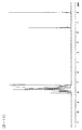
- FIG. 1 is a 1 H-NMR spectrum diagram of a compound 2-11 of the present invention.
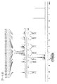
- FIG. 1 is a 1 H-NMR spectrum of a compound (7-13) of the present invention.
- the charge transport material of the present invention has a structure represented by the following general formula (1), and has 6 to 19 monocyclic aromatic rings (the aromatic ring is a carbon atom or a nitrogen atom) , Having a ring member of 6) (hereinafter, also referred to as a compound represented by the general formula (1)).
- General formula (1) Although the charge transport material of the present invention has such a structure, it is not bound by any theory, but by introducing an electron withdrawing group, the electron affinity is increased and a low driving voltage of the device can be achieved. Estimated. Further, by having such a configuration, the durability of the element is improved, although it is not limited to any theory. Therefore, the organic electroluminescent element using the charge transport material of the present invention is excellent in driving voltage and durability.
- the charge transport material represented by the general formula (1) can be preferably used for organic electronic elements such as electrophotography, organic transistors, organic photoelectric conversion elements (for energy conversion, sensor applications, etc.), and organic electroluminescence elements.
- the organic electroluminescence device is particularly preferably used.
- the charge transport material of the present invention can also be used for a thin film containing the compound represented by the general formula (1).
- the thin film can be formed using the composition by a dry film forming method such as a vapor deposition method or a sputtering method, or a wet film forming method such as a transfer method or a printing method.
- the thickness of the thin film may be any thickness depending on the application, but is preferably 0.1 nm to 1 mm, more preferably 0.5 nm to 1 ⁇ m, still more preferably 1 nm to 200 nm, and particularly preferably 1 nm to 100 nm. is there.
- the hydrogen atom in the description of the general formula (1) includes an isotope (deuterium atom and the like), and the atoms constituting the substituent further include the isotope.
- the substituent when referred to as “substituent”, the substituent may be substituted.
- the term “alkyl group” in the present invention includes an alkyl group substituted with a fluorine atom (for example, trifluoromethyl group) and an alkyl group substituted with an aryl group (for example, triphenylmethyl group).
- alkyl group having 1 to 6 carbon atoms it means that all groups including substituted ones have 1 to 6 carbon atoms.
- the charge transport material of the present invention relates to a structure represented by the general formula (1).
- R 111 to R 128 represent a hydrogen atom or a substituent. At least one of R 111 to R 122 is a cyano group.
- Examples of the substituent include a cyano group, an alkyl group having 1 to 10 carbon atoms, a halogen atom, and an aryl group having 6 to 30 carbon atoms.
- a methyl group, an ethyl group, an isopropyl group, an n-propyl group, a t-butyl group, a s-butyl group, and an n-butyl group are preferable, and a methyl group, an ethyl group, an isopropyl group, and a t-butyl group are preferable. More preferred are a methyl group and a t-butyl group, and a methyl group is particularly preferred.
- the halogen atom a fluorine atom is preferable.
- the aryl group having 6 to 30 carbon atoms is preferably an aryl group that is unsubstituted or substituted with a cyano group, and as a further condition, a chain aryl group (one benzene ring is substituted with 3 or more benzene rings). More preferred).
- the substituent is preferably a cyano group, an alkyl group or an aryl group, more preferably a cyano group or an aryl group.
- the T 1 energy in the film state of the compound represented by the general formula (1) is preferably 56 kcal / mol or more and 80 kcal / mol or less, more preferably 57 kcal / mol or more and 70 kcal / mol or less, More preferably, it is 58 kcal / mol or more and 66 kcal / mol or less.
- the T 1 energy is preferably in the above range.
- the T 1 energy can be determined from the short wavelength end of a phosphorescence emission spectrum of a thin film of material. For example, a material is deposited on a cleaned quartz glass substrate to a thickness of about 50 nm by vacuum deposition, and the phosphorescence emission spectrum of the thin film is measured at F-7000 Hitachi Spectrofluorimeter (Hitachi High Technologies) under liquid nitrogen temperature. Use to measure. T 1 energy can be obtained by converting the rising wavelength on the short wavelength side of the obtained emission spectrum into energy units.
- the molecular weight of the compound represented by the general formula (1) is preferably 1000 or less, more preferably 500 to 1000, and particularly preferably 600 to 900. . By setting the molecular weight within this range, a material having good film quality and excellent sublimation purification / deposition suitability can be obtained.
- the molecular weight of the compound represented by the general formula (1) is preferably 600 to 1000 from the viewpoint of deposition suitability.
- the glass transition temperature (Tg) of the compound represented by the general formula (1) is 80 ° C. or higher and 400 ° C. or lower (from the viewpoint of stably operating the organic electroluminescence device against heat generated during high temperature driving or driving the device) Or not detected), more preferably 100 ° C. or higher and 400 ° C. or lower (or not detected), and even more preferably 110 ° C. or higher and 400 ° C. or lower (or not detected).
- the purity of the compound represented by the general formula (1) is high.
- the purity can be measured by, for example, high performance liquid chromatography (HPLC), and the area ratio of the compound represented by the general formula (1) when detected with a light absorption intensity of 254 nm is preferably 99.00% or more, and more It is preferably 99.50% or more, particularly preferably 99.90% or more, and most preferably 99.9% or more.
- a material in which part or all of the hydrogen atoms of the compound represented by the general formula (1) are substituted with deuterium atoms is also preferably charged. It can be used as a transport material.
- the compound represented by the general formula (1) may belong to two or more of the following general formulas (1A-1) to (1A-20).
- the compound represented by the general formula (1) can be synthesized by combining the method described in JP-A-2007-266598 and other known reactions. After synthesis, it is preferable to purify by sublimation purification after purification by column chromatography, recrystallization or the like. By sublimation purification, not only can organic impurities be separated, but inorganic salts and residual solvents can be effectively removed.
- the organic electroluminescent element of the present invention has a substrate, a pair of electrodes including an anode and a cathode disposed on the substrate, and an organic layer disposed between the electrodes, and the organic layer emits phosphorescence. It contains the material and the charge transport material of the present invention, that is, the compound represented by the general formula (1).
- R 111 to R 128 each represent a hydrogen atom or a substituent. At least one of R 111 to R 122 is a cyano group, provided that each of the three consecutive benzene rings has a cyano group. The benzene ring having a cyano group is not substituted with three or more benzene rings.
- the structure of the organic electroluminescent element of the present invention is not particularly limited.
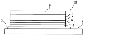
- FIG. 1 an example of a structure of the organic electroluminescent element of this invention is shown. 1 has an organic layer on a substrate 2 between a pair of electrodes (anode 3 and cathode 9).
- the element configuration, the substrate, the cathode, and the anode of the organic electroluminescence element are described in detail in, for example, Japanese Patent Application Laid-Open No. 2008-270736, and the matters described in the publication can be applied to the present invention.
- the preferable aspect of the organic electroluminescent element of this invention is demonstrated in detail in order of a board
- the organic electroluminescent element of the present invention has a substrate.
- the substrate used in the present invention is preferably a substrate that does not scatter or attenuate light emitted from the organic layer.
- the organic electroluminescent element of the present invention is disposed on the substrate and has a pair of electrodes including an anode and a cathode.
- a pair of electrodes including an anode and a cathode.
- at least one of the pair of electrodes, the anode and the cathode is preferably transparent or translucent.
- the anode usually only needs to have a function as an electrode for supplying holes to the organic layer, and there is no particular limitation on the shape, structure, size, etc., depending on the use and purpose of the light-emitting element, It can select suitably from well-known electrode materials.
- the anode is usually provided as a transparent anode.
- the cathode usually has a function as an electrode for injecting electrons into the organic layer, and there is no particular limitation on the shape, structure, size, etc., and it is known depending on the use and purpose of the light-emitting element.
- the electrode material can be selected as appropriate.
- the organic electroluminescent element of the present invention has an organic layer disposed between the electrodes, and the organic layer includes a phosphorescent material and a compound represented by the general formula (1).
- the organic layer includes a phosphorescent material and a compound represented by the general formula (1).
- the organic layer is formed on the entire surface or one surface of the transparent electrode or the semitransparent electrode.
- the organic layer is formed on the entire surface or one surface of the transparent electrode or the semitransparent electrode.
- the configuration of the organic layer, the method for forming the organic layer, preferred embodiments of the layers constituting the organic layer, and materials used for the layers will be described in order.
- the organic layer preferably includes a charge transport layer.
- the charge transport layer is a layer in which charge transfer occurs when a voltage is applied to the organic electroluminescent element. Specific examples include a hole injection layer, a hole transport layer, an electron block layer, a light emitting layer, a hole block layer, an electron transport layer, and an electron injection layer. A hole injection layer, a hole transport layer, an electron blocking layer, or a light emitting layer is preferable. If the charge transport layer formed by the coating method is a hole injection layer, a hole transport layer, an electron blocking layer, or a light emitting layer, it is possible to manufacture an organic electroluminescent element with low cost and high efficiency.
- the charge transport layer is more preferably a hole injection layer, a hole transport layer, or an electron block layer.
- the organic electroluminescent element of the present invention preferably has a light emitting layer containing the phosphorescent material and another organic layer, and the light emitting layer contains the compound represented by the general formula (1). Furthermore, in the organic electroluminescent element of the present invention, it is more preferable that the organic layer has a light emitting layer containing the phosphorescent material and another organic layer. However, in the organic electroluminescent element of the present invention, even when the organic layer has a light emitting layer and other organic layers, the layers do not necessarily have to be clearly distinguished.
- the organic layer contains a phosphorescent material and a compound represented by the general formula (1).
- the said organic layer has the light emitting layer containing the said phosphorescence-emitting material, and another organic layer, and the said light emitting layer contains the compound represented by the said General formula (1).
- the compound represented by the general formula (1) is used as a host material of the light emitting layer (hereinafter also referred to as a host compound).
- the compound represented by the general formula (1) is not limited in its application, and may be contained in any layer in the organic layer between the cathode and the anode of the organic electroluminescence device.
- the introduction layer of the compound represented by the general formula (1) is preferably contained in one or more of the light emitting layer, the layer between the light emitting layer and the cathode, and the layer between the light emitting layer and the anode.
- the compound represented by the general formula (1) is added to the light emitting layer, the organic layer adjacent to the light emitting layer between the light emitting layer and the cathode (the cathode side layer adjacent to the light emitting layer), and the light emitting layer side.
- the compound represented by the general formula (1) may be contained in both the light emitting layer and the cathode side layer adjacent to the light emitting layer.
- the compound represented by the general formula (1) is contained in the light emitting layer as a host material of the light emitting layer.
- the compound represented by the general formula (1) is 0.1 to 99 mass with respect to the total mass of the light emitting layer. %, Preferably 1 to 97% by mass, more preferably 10 to 96% by mass.
- the LUMO level is preferably in the range of ⁇ 1.90 eV or more and less than ⁇ 1.20 eV from the viewpoint of lowering the voltage and light emission efficiency. More preferably, the range is from ⁇ 1.80 eV to less than ⁇ 1.30 eV, and even more preferably from ⁇ 1.70 eV to less than ⁇ 1.40 eV. This is because the electron injection property from the electron transport layer to the light emitting layer is improved and the driving voltage is lowered.
- the specific LUMO level (lowest orbital energy) of the compound represented by the general formula (1) described in this specification is B3LYP / 6-31G (d) // B3LYP / 6-31G (d ) Is the value obtained by performing quantum chemical calculations at the level. Even with the same electron-withdrawing group, the degree of increasing the LUMO level varies depending on the substitution position.
- the LUMO level described above includes that the light emitting layer includes a partial structure represented by the following general formula (1A) as a compound having the structure represented by the general formula (1) as a host material of the light emitting layer. It is more preferable from the viewpoint of realizing a range of -1.90 eV or more and less than -1.20 eV.
- partial structures represented by the general formula (1) partial structures represented by the following general formulas (1A-1) to (1A-20), which are more preferable partial structures, are shown below.
- the invention is not limited to the following specific examples.
- the partial structure represented by the following general formula (1A-1) is ⁇ 1.51 eV
- the partial structure represented by (1A-3) is -1.58 eV
- the partial structure represented by the following general formula (1A-5) is -1.56 eV
- the partial structure represented is ⁇ 1.54 eV
- the partial structure represented by the following general formula (1A-7) is ⁇ 1.76 eV.
- the partial structure represented by the following general formula (1A-11) is ⁇ 1.87 eV
- the partial structure represented by the following general formula (1A-12) is ⁇ 1.85 eV
- the following general formula (1A- The partial structure represented by 13) is -1.73 eV
- the partial structure represented by the following general formula (1A-14) is -1.75 eV
- the partial structure is -1.91 eV
- the partial structure represented by the following general formula (1A-18) is -1.79 eV
- the partial structure represented by the following general formula (1A-19) is -1.
- the partial structure represented by the following general formula (1A-20) is -2.01 eV.
- the maximum light emission wavelength (hereinafter also referred to as emission peak wavelength) of the light emitting material is preferably 400 to 700 nm, and 470 to 650 nm. Is more preferably 490 to 620 nm, and most preferably 500 to 610 nm.
- the organic layer includes a light emitting layer containing the phosphorescent material and another organic layer, and the other organic layer disposed between the light emitting layer and the cathode is represented by the general formula (1). It is also preferable to contain a compound having a structure. Among them, the organic layer has an electron transport layer or a hole blocking layer (more preferably, a hole blocking layer), and the electron transport layer or the hole blocking layer is represented by the general formula (1). It is more preferable to contain.
- the compound represented by the general formula (1) is contained in a layer other than the light emitting layer, it is preferably contained in an amount of 70 to 100% by mass, based on the total mass of the layer other than the light emitting layer, and 80 to 100% by mass. % Is more preferable.
- the LUMO level is preferably in the range of ⁇ 2.10 eV or more and less than ⁇ 1.50 eV, preferably ⁇ 2.00 eV or more and less than ⁇ 1.55 eV. Is more preferable, and a range of ⁇ 1.90 eV or more and less than ⁇ 1.60 eV is even more preferable. This is because the electron injecting property from the cathode to the electron transporting layer is improved and the electron injecting property to the light emitting layer is improved.
- the other organic layer disposed between the light emitting layer and the cathode includes a partial structure represented by the general formula (1A) as a compound having a structure represented by the general formula (1). Is preferable from the viewpoint of realizing the above-mentioned LUMO level of ⁇ 2.10 eV or more and less than ⁇ 1.50 eV.
- another organic layer disposed between the light emitting layer and the cathode is represented by the general formula (1).
- the present invention is not limited to the following specific examples.
- positioned between the said light emitting layer and the said cathode is represented by the said partial structure group (1A) as a compound of the structure represented by the said General formula (1). It is also preferable to contain a compound having a partial structure.
- These organic layers may be provided in a plurality of layers, and when a plurality of layers are provided, they may be formed of the same material or different materials for each layer.
- each organic layer is formed by a dry film forming method such as a vapor deposition method or a sputtering method, a wet film forming method such as a transfer method, a printing method, a spin coating method, or a bar coating method (solution coating method). Any of these can be suitably formed.
- the organic layer disposed between the pair of electrodes includes at least one layer formed by vapor deposition of a composition containing the compound represented by the general formula (1). Is preferred.
- the light emitting layer receives holes from the anode, hole injection layer or hole transport layer and receives electrons from the cathode, electron injection layer or electron transport layer when an electric field is applied, and provides a field for recombination of holes and electrons. And a layer having a function of emitting light.
- the light emitting layer in the present invention is not necessarily limited to light emission by such a mechanism.
- the light emitting layer in the organic electroluminescent element of the present invention preferably contains at least one phosphorescent material.
- the light emitting layer in the organic electroluminescent device of the present invention may be composed only of the light emitting material, or may be a mixed layer of a host material and the light emitting material.
- the kind of the light emitting material may be one kind or two kinds or more.
- the host material is preferably a charge transport material.
- the host material may be one kind or two or more kinds, and examples thereof include a configuration in which an electron transporting host material and a hole transporting host material are mixed.
- the light emitting layer may include a material that does not have charge transporting properties and does not emit light.
- the light emitting layer may be a single layer or a multilayer of two or more layers, and each layer may contain the same light emitting material or host material, or each layer may contain a different material. When there are a plurality of light emitting layers, each of the light emitting layers may emit light with different emission colors.
- the thickness of the light emitting layer is not particularly limited, but is usually preferably 2 nm to 500 nm, and more preferably 3 nm to 200 nm, and more preferably 5 nm to 100 nm from the viewpoint of external quantum efficiency. More preferably.
- the light emitting layer contains a compound represented by the general formula (1), and the host material of the light emitting layer is represented by the general formula (1). It is a more preferable embodiment to use a compound.
- the host material is a compound mainly responsible for charge injection and transport in the light emitting layer, and is a compound that itself does not substantially emit light.
- substantially does not emit light means that the amount of light emitted from the compound that does not substantially emit light is preferably 5% or less, more preferably 3% or less of the total amount of light emitted from the entire device. Preferably it says 1% or less.
- the host material other than the light emitting material and the compound represented by the general formula (1) will be described in order.
- the compound represented by the said General formula (1) may be used other than the said light emitting layer in the organic electroluminescent element of this invention.
- Luminescent material As the light emitting material in the present invention, any of phosphorescent light emitting materials, fluorescent light emitting materials and the like can be used.
- the light emitting layer in the present invention can contain two or more kinds of light emitting materials in order to improve the color purity and broaden the light emission wavelength region. At least one of the light emitting materials is preferably a phosphorescent light emitting material.
- a fluorescent light-emitting material or a phosphorescent light-emitting material different from the phosphorescent light-emitting material contained in the light-emitting layer can be used as the light-emitting material.
- Examples of phosphorescent light-emitting materials that can be used in the present invention include US Pat. / 19373A2, JP-A No. 2001-247859, JP-A No. 2002-302671, JP-A No. 2002-117978, JP-A No. 2003-133074, JP-A No. 2002-1235076, JP-A No. 2003-123684, JP-A No. 2002-170684, EP No. 121157, JP-A No.
- luminescent materials include iridium (Ir) complexes, platinum (Pt) complexes, Cu complexes, and Re complexes.
- iridium (Ir) complex W complexes, Rh complexes, Ru complexes, Pd complexes, Os complexes, Eu complexes, Tb complexes, Gd complexes, Dy complexes, and Ce complexes.
- an iridium (Ir) complex a platinum (Pt) complex, or a Re complex.
- at least one coordination mode of a metal-carbon bond, a metal-nitrogen bond, a metal-oxygen bond, or a metal-sulfur bond is used.
- An iridium (Ir) complex, a platinum (Pt) complex, or a Re complex is preferable.
- iridium (Ir) complex and platinum (Pt) complex are particularly preferable, and iridium (Ir) complex is most preferable from the viewpoint of luminous efficiency, driving durability, chromaticity and the like.
- Z 1 and Z 2 each independently represents a carbon atom or a nitrogen atom.
- a 1 represents an atomic group that forms a 5- or 6-membered heterocycle with Z 1 and a nitrogen atom.
- B 1 represents an atomic group that forms a 5- or 6-membered ring with Z 2 and a carbon atom.
- Z 1 and Z 2 each independently represents a carbon atom or a nitrogen atom.
- (XY) represents a monoanionic bidentate ligand.
- n E1 represents an integer of 1 to 3.
- Z 1 and Z 2 are preferably carbon atoms.
- n E1 is preferably 2 or 3, in which case there are two or three ligands containing Z 1 , Z 2 , A 1 , B 1, which are the same as each other May be different.
- Examples of the 5- or 6-membered heterocycle containing A 1 , Z 1 and a nitrogen atom include a pyridine ring, pyrimidine ring, pyrazine ring, triazine ring, imidazole ring, pyrazole ring, oxazole ring, thiazole ring, triazole ring, oxadiazole Ring, thiadiazole ring and the like.
- the 5- or 6-membered heterocycle formed by A 1 , Z 1 and a nitrogen atom may have a substituent.
- Examples of the 5- or 6-membered ring formed by B 1 , Z 2 and a carbon atom include a benzene ring, a pyridine ring, a pyrimidine ring, a pyrazine ring, a pyridazine ring, a triazine ring, an imidazole ring, a pyrazole ring, an oxazole ring, a thiazole ring, Examples include a triazole ring, an oxadiazole ring, a thiadiazole ring, a thiophene ring, a furan ring, and a pyrrole ring.
- the 5- or 6-membered ring formed by B 1 , Z 2 and a carbon atom may have a substituent.
- the substituents may be linked to form a ring.
- the ring formed include an unsaturated 4- to 7-membered ring, a benzene ring, a pyridine ring, a pyrazine ring, a pyridazine ring, a pyrimidine ring, an imidazole ring, Examples thereof include an oxazole ring, a thiazole ring, a pyrazole ring, a thiophene ring, and a furan ring.
- These formed rings may have a substituent, and may further form a ring via a substituent on the formed ring.
- a 5- or 6-membered heterocyclic substituent formed by A 1 , Z 1 and a nitrogen atom, and a 5- or 6-membered ring substituent formed by B 1 , Z 2 and a carbon atom may be linked to form a condensed ring similar to that described above.
- a ring may be further formed through a substituent on the formed ring.
- Substituent group A An alkyl group (preferably having 1 to 30 carbon atoms, more preferably 1 to 20 carbon atoms, particularly preferably 1 to 10 carbon atoms, such as methyl, ethyl, isopropyl, t-butyl, n-octyl, n-decyl, n-hexadecyl, cyclopropyl, cyclopentyl, cyclohexyl, etc.), alkenyl groups (preferably having 2 to 30 carbon atoms, more preferably 2 to 20 carbon atoms, particularly preferably 2 to 10 carbon atoms, such as vinyl , Allyl, 2-butenyl, 3-pentenyl, etc.), alkynyl group (preferably having 2 to 30 carbon atoms, more preferably 2 to 20 carbon atoms, particularly preferably 2 to 10 carbon atoms such as propargyl , 3-pentynyl, etc.), aryl groups (preferably having 6 to 30 carbon atom
- Particularly preferably 0 to 10 carbon atoms such as amino, methylamino, dimethylamino, diethylamino, dibenzylamino, diphenylamino, ditolylamino, etc.
- an alkoxy group preferably having 1 to 30 carbon atoms, Preferably it has 1 to 20 carbon atoms, particularly preferably 1 to 10 carbon atoms, and examples thereof include methoxy, ethoxy, butoxy, 2-ethylhexyloxy, etc.
- an aryloxy group preferably having 6 to 30 carbon atoms, More preferably, it has 6 to 20 carbon atoms, particularly preferably 6 to 12 carbon atoms.
- heterocyclic oxy group preferably having 1 to 30 carbon atoms, more preferably 1 to 20 carbon atoms, and particularly preferably 1 to 12 carbon atoms.
- a heterocyclic oxy group preferably having 1 to 30 carbon atoms, more preferably 1 to 20 carbon atoms, and particularly preferably 1 to 12 carbon atoms.
- an acyl group preferably having 2 to 30 carbon atoms, more preferably 2 to 20 carbon atoms, and particularly preferably 2 to 12 carbon atoms.
- Benzoyl, formyl, pivaloyl, etc. an alkoxycarbonyl group (preferably having 2 to 30 carbon atoms, more preferably 2 to 20 carbon atoms, particularly preferably 2 to 12 carbon atoms such as methoxycarbonyl, ethoxy Carbonyl, etc.), an aryloxycarbonyl group (preferably having a carbon number)
- the number of carbon atoms is 7 to 30, more preferably 7 to 20, and particularly preferably 7 to 12, and examples thereof include phenyloxycarbonyl.
- An acyloxy group (preferably having 2 to 30 carbon atoms, more preferably 2 to 20 carbon atoms, particularly preferably 2 to 10 carbon atoms, such as acetoxy, benzoyloxy, etc.), an acylamino group (preferably 2-30 carbon atoms, more preferably 2-20 carbon atoms, particularly preferably 2-10 carbon atoms, and examples thereof include acetylamino, benzoylamino and the like, and alkoxycarbonylamino groups (preferably having 2-2 carbon atoms).
- an aryloxycarbonylamino group preferably having 7 to 30 carbon atoms, more preferably 7 to 20 carbon atoms, particularly preferably 7 to 12 carbon atoms, for example phenyloxycarbonyl And sulfonylamino groups (preferably having 1 to 30 carbon atoms, more preferably 1 to 20 carbon atoms, particularly preferably 1 to 12 carbon atoms, such as methanesulfonylamino and benzenesulfonylamino).
- an aryloxycarbonylamino group preferably having 7 to 30 carbon atoms, more preferably 7 to 20 carbon atoms, particularly preferably 7 to 12 carbon atoms, for example phenyloxycarbonyl And sulfonylamino groups (preferably having 1 to 30 carbon atoms, more preferably 1 to 20 carbon atoms, particularly preferably 1 to 12 carbon atoms, such as methanesulfonylamino and benzenesulfonylamino).
- a sulfamoyl group (preferably having 0 to 30 carbon atoms, more preferably 0 to 20 carbon atoms, particularly preferably 0 to 12 carbon atoms, such as sulfamoyl, methylsulfamoyl, dimethylsulfamoyl, phenyl Sulfamoyl, etc.), carbamoyl groups (preferably having 1 to 30 carbon atoms, more preferably 1 to 20 carbon atoms, particularly preferably 1 to 12 carbon atoms, such as carbamoyl, methylcarbamoyl, diethylcarbamoyl, Phenylcarbamoyl etc.), alkylthio group ( Preferably, it has 1 to 30 carbon atoms, more preferably 1 to 20 carbon atoms, particularly preferably 1 to 12 carbon atoms, such as methylthio, ethylthio, etc.), an arylthio group (preferably 6 to 30 carbon atoms).
- Rufinyl group (preferably having 1 to 30 carbon atoms, more preferably 1 to 20 carbon atoms, particularly preferably 1 to 12 carbon atoms, and examples thereof include methanesulfinyl and benzenesulfinyl. ), A ureido group (preferably having 1 to 30 carbon atoms, more preferably 1 to 20 carbon atoms, particularly preferably 1 to 12 carbon atoms, such as ureido, methylureido, phenylureido, etc.), phosphoric acid An amide group (preferably having 1 to 30 carbon atoms, more preferably 1 to 20 carbon atoms, particularly preferably 1 to 12 carbon atoms, such as diethyl phosphoric acid amide and phenyl phosphoric acid amide), a hydroxy group , Mercapto group, halogen atom (eg fluorine atom, chlorine atom, bromine atom, iodine atom), cyano group, sulfo group, carb
- Is for example, a nitrogen atom, oxygen atom, sulfur atom, phosphorus atom, silicon atom, selenium atom, tellurium atom, specifically pyridyl, pyrazinyl, pyrimidyl, pyridazinyl, pyrrolyl, pyrazolyl, triazolyl, imidazolyl, oxazolyl, thiazolyl, And isoxazolyl, isothiazolyl, quinolyl, furyl, thienyl, selenophenyl, tellurophenyl, piperidyl, piperidino, morpholino, pyrrolidyl, pyrrolidino, benzoxazolyl, benzoimidazolyl, benzothiazolyl, carbazolyl group, azepinyl group, silolyl group and the like.
- a silyl group (preferably having 3 to 40 carbon atoms, more preferably 3 to 30 carbon atoms, particularly preferably 3 to 24 carbon atoms, and examples thereof include trimethylsilyl and triphenylsilyl).
- a aryloxy group (preferably having 3 to 40 carbon atoms, more preferably 3 to 30 carbon atoms, particularly preferably 3 to 24 carbon atoms, such as trimethylsilyloxy, triphenylsilyloxy, etc.), phosphoryl group (for example, A diphenylphosphoryl group, a dimethylphosphoryl group, etc.).
- These substituents may be further substituted, and examples of the further substituent include a group selected from the substituent group A described above.
- the substituent substituted by the substituent may be further substituted, and examples of the further substituent include a group selected from the substituent group A described above.
- the substituent substituted by the substituent substituted by the substituent may be further substituted, and examples of the further substituent include a group selected from the substituent group A described above.
- Rx, Ry and Rz each independently represents a hydrogen atom or a substituent.
- substituent include a substituent selected from the substituent group A.
- Rx and Rz are preferably each independently an alkyl group, a perfluoroalkyl group, or an aryl group.
- Ry is preferably any one of a hydrogen atom, an alkyl group, a perfluoroalkyl group, a fluorine atom, a cyano group, and an aryl group.
- a plurality of Rx and Ry existing in one ligand may be the same or different.
- Ry may be bonded to each other to form a ring.
- Rx are not bonded to each other.
- Ligands having these ligands can be synthesized in the same manner as in known synthesis examples by using corresponding ligand precursors.
- a preferred embodiment of the iridium (Ir) complex represented by the general formula (E-1) is an iridium (Ir) complex represented by the following general formula (E-2).
- a E1 to A E8 each independently represents a nitrogen atom or C—R E.
- R E represents a hydrogen atom or a substituent.
- substituent those exemplified as the substituent group A can be applied.
- R E may be connected to each other to form a ring. Examples of the ring formed include the same ring as the condensed ring described in the general formula (E-1).
- (X-Y) and n E2 is (X-Y) in Formula (E1) have the same meanings as and n E1, preferred ranges are also the same.
- n E2 is 2 or 3
- there are two or three ligands containing A E1 to A E8, and these ligands may be the same or different.
- a more preferred form of the compound represented by the general formula (E-2) is a compound represented by the following general formula (E-3).
- R T1 , R T2 , R T3 , R T4 , R T5 , R T6, and R T7 have the same meaning as R E.
- A represents CR ′′ ′′ or a nitrogen atom, and R ′′ ′′ has the same meaning as RE.
- R T1 to R T7 and R ′′ ′′ may be bonded to any two adjacent to each other to form a condensed 4- to 7-membered ring.
- a fused 4- to 7-membered ring may further have a substituent represented by the substituent group A.
- (XY) and n E3 have the same meanings as (XY) and n E1 in formula (E-1), and the preferred ranges are also the same.
- n E3 is 2 or 3
- the ligands may be the same as or different from each other.
- the preferable range of A and R T1 to R T7 varies depending on the emission color required according to the application. In the following, description will be given by dividing into three regions of blue to light blue, green to yellow, yellow orange to red as target emission colors. However, it is not limited to these descriptions.
- R T1 to R T4 , R T7 , A (CR ′′ ′′ or a nitrogen atom), (XY) and n E4 in the general formula (E-4) are R T1 to R T1 in the general formula (E-3). It is synonymous with R T4 , R T7 , A, (XY) and n E3 .
- R 1 ′ to R 4 ′ have the same meaning as R E.
- R T1 to R T4 , R T7 , R 1 ′ to R 4 ′ and R ′′ ′′ may be bonded to each other to form a condensed 4- to 7-membered ring.
- the 7-membered ring is cycloalkene, cyclocarbadiene, aryl, or heteroaryl, and the fused 4- to 7-membered ring may further have a substituent represented by Substituent Group A.
- n E4 is 2 or 3
- R 1 ′ to R 4 ′ are preferably a hydrogen atom, a fluorine atom, an alkyl group, or an aryl group. Further, it is preferable that A represents CR ′′ ′′, and 0 to 3 of R T1 to R T4 , R T7 and R ′′ ′′ are an alkyl group or a phenyl group, and the rest are all hydrogen atoms.
- R T2 to R T6 , A (CR ′′ ′′ or nitrogen atom), (XY) and n E5 in the general formula (E-5) are R T2 to R T6 in the general formula (E-3), Synonymous with A, (XY) and n E3 .
- R 5 ′ to R 8 ′ have the same meanings as R 1 ′ to R 4 ′ in formula (E-4).
- R T2 to R T6 , R 5 ′ to R 8 ′, and R ′′ ′′ may be bonded to each other to form a condensed 4- to 7-membered ring.
- the ring is a cycloalkene, cyclocarbadiene, aryl or heteroaryl, and the condensed 4- to 7-membered ring may further have a substituent represented by the substituent group A.
- n E5 is 2 or 3
- the preferred range for R 5 ′ to R 8 ′ is the same as the preferred range for R 1 ′ to R 4 ′ in formula (E-4).
- A represents CR ′′ ′′, and among R T2 to R T6 , R ′′ ′′, and R 5 ′ to R 8 ′, 0 to 3 are alkyl groups or phenyl groups, and the rest are all hydrogen atoms. Is preferred.
- R T1 to R T5 , A (CR ′′ ′′ or nitrogen atom), (XY) and n E6 in the general formula (E-6) are R T1 to R T5 in the general formula (E-3), Synonymous with A, (XY) and n E3 .
- R 9 ′ to R 12 ′ have the same meanings as R 1 ′ to R 4 ′ in formula (E-4).
- R T1 to R T5 , R 9 ′ to R 12 ′, and R ′′ ′′ may be bonded to each other to form a condensed 4- to 7-membered ring.
- the ring is a cycloalkene, cyclocarbadiene, aryl or heteroaryl, and the condensed 4- to 7-membered ring may further have a substituent represented by the substituent group A.
- n E6 is 2 or 3
- the preferred range for R 9 ′ to R 12 ′ is the same as the preferred range for R 1 ′ to R 4 ′ in formula (E-4).
- A represents CR ′′ ′′, and among R T1 to R T5 , R ′′ ′′, and R 9 ′ to R 12 ′, 0 to 3 are alkyl groups or phenyl groups, and the rest are all hydrogen atoms. Is preferred.
- R T1 , R T2 , R T3 , R T4 , R T5 , R T6 , R T7 , R ′′ ′′, (XY) and n E3 are represented by the general formula (E ⁇ It is synonymous with R T1 , R T2 , R T3 , R T4 , R T5 , R T6 , R T7 , R ′′ ′′, (XY) and n E3 in 3 ).
- R T1 to R T7 and R ′′ ′′ may be bonded to any two adjacent to each other to form a condensed 4- to 7-membered ring.
- a fused 4- to 7-membered ring may further have a substituent represented by the substituent group A.
- n E7 is 2 or 3
- the ligands may be the same or different from each other.
- R T1 , R T2 , R T3 , R T4 , R T5 , R T6 , R T7 , R ′′ ′′ may be a hydrogen atom, a fluorine atom, an alkyl group, an aryl group, a heteroaryl group, or a cyano group preferable.
- n E7 is preferably 3, and the general formula (E-7) is preferably a compound represented by the general formula (E-7-1).
- R T1 , R T2 , R T3 , R T4 , R T5 , R T6 , R T7 , R ′′ ′′ are R T1 in the general formula (E-7), R T2 , R T3 , R T4 , R T5 , R T6 , R T7 , R ′′ ′′ have the same meanings and preferred ranges.
- R T8 to R T15 are synonymous with R T1 , R T2 , R T3 , R T4 , R T5 , R T6 , R T7 , R ′′ ′′ and the preferred ranges are also the same, but R T1 , R T2 , A phenylpyridine ligand containing R T3 , R T4 , R T5 , R T6 , R T7 , R ′′ ′′ and a phenylpyridine ligand containing R T8 to R T15 are different from each other.
- R T1 , R T2 , R T3 , R T4 , R T5 , R T6 , R T7 , R ′′ ′′ are hydrogen atoms, A fluorine atom, an alkyl group, and a cyano group are more preferable, and 1 to 3 of R T1 , R T5 , R T4 , and R ′′ ′′ are more preferably an alkyl group.
- R T8 to R T11 are more preferably a hydrogen atom or an alkyl group.
- R T12 to R T15 are more preferably a hydrogen atom, an alkyl group, a cyano group, or an aryl group.
- the substitution position of the alkyl group, cyano group or aryl group is preferably R T13 or R T14 .
- the aryl group may further have a substituent, and may form a condensed ring through the substituent.
- R T1 , R T2 , R T3 , R T4 , R T5 , R T6 , R T7 , R ′′ ′′ are hydrogen atoms, It is more preferably an alkyl group, and more preferably 1 to 3 of R T1 , R T5 , R T4 and R ′′ ′′ are alkyl groups. It is more preferable that at least one of R T8 to R T11 is an aryl group, and it is more preferable that any one of R T9 and R T10 is an aryl group and the remaining is a hydrogen atom or an alkyl group.
- the aryl group may further have a substituent, and may form a condensed ring through the substituent.
- the general formula (E-7-1) preferably has a partial structure represented by the general formula (E-7-2) in the general formula (E-7-1).
- effects such as low voltage and high durability may be noticeable depending on the combination with the host material.
- any one of R T16 to R T28 is preferably bonded to a part of general formula (E-7-1) via a single bond or an aryl group,
- R T13 or R T14 When it is desired to obtain a light emission color close to, it is more preferable to bond with R T13 or R T14 , and further preferable to bond with R T13 .
- R T9 or R T10 When it is desired to obtain a light emission color close to yellow, it is more preferable to bond with R T9 or R T10 .
- X is preferably —O—, —S—, —NR T24 —, —CR T25 R T26 —, and more preferably —O—, —S—.
- X When X is —O— or —S—, it is preferably bonded to a part of formula (E-7-1) through a single bond at the position of R T16 , and X is —NR T24 — In this case, it is preferable to bond to a part of the general formula (E-7-1) through a single bond at the position of R T18 or R T24 , and when X is —CR T25 R T26 —, R T17 It is preferable to bond to a part of the general formula (E-7-1) through a single bond at the position.
- R T1 , R T2 , R T3 , R T4 , R T5 , R T6 , R T7 , A (CR ′′ ′′ or nitrogen atom), (XY), n E8 Is synonymous with R T1 , R T2 , R T3 , R T4 , R T5 , R T6 , R T7 , A, (XY), and n E3 in the general formula (E-3).
- R T1 and R T5 to R T7 are more preferably a hydrogen atom, an alkyl group, or an aryl group.
- R T2 to R T4 are preferably a hydrogen atom, a fluorine atom, or a cyano group.
- R ′′ ′′ of CR ′′ ′′ is preferably a fluorine atom or a cyano group, or a nitrogen atom.
- n E8 is preferably 2 or 3.
- (XY) has the same meaning as (XY) in formula (E-1), and the preferred range is also the same.
- R T29 to R T34 , (XY), and n E8 have the same meanings as R T1 to R T6 (XY) and n E3 in the general formula (E-3).
- R T35 represents a substituent, and examples of the substituent include the substituent group B.
- R T29 to R T35 may combine any two adjacent to each other to form a condensed 4- to 7-membered ring, and the fused 4- to 7-membered ring is a cycloalkene, cyclocarbadiene, aryl or heteroaryl
- the condensed 4- to 7-membered ring may further have a substituent represented by the substituent group A.
- n E7 is 2 or 3
- the ligands may be the same or different from each other.
- R T29 to R T34 are preferably a hydrogen atom, an alkyl group, an aryl group, or a cyano group.
- R T35 is preferably an alkyl group or an aryl group.
- R T35 is preferably linked to R T29 to form a ring, and R T35 and R T29 are more preferably bonded via an aryl group, resulting in the formation of a nitrogen-containing 6-membered ring.
- the aryl group linked to R T29 may further have a substituent, and is more preferably substituted with an alkyl group from the viewpoint of durability.
- the compounds exemplified as the compound represented by the general formula (E-1) can be synthesized by the method described in JP2009-99783A, various methods described in US Pat. No. 7,279,232 and the like. After synthesis, it is preferable to purify by sublimation purification after purification by column chromatography, recrystallization or the like. By sublimation purification, not only can organic impurities be separated, but inorganic salts and residual solvents can be effectively removed.
- the compound represented by the general formula (E-1) is preferably contained in the light emitting layer, but its use is not limited, and may be further contained in any layer in the organic layer. .
- the compound represented by the general formula (E-1) in the light emitting layer is generally contained in the light emitting layer in an amount of 0.1% by mass to 50% by mass with respect to the total mass of the compound forming the light emitting layer.
- the content is preferably 0.2% by mass to 50% by mass, more preferably 0.3% by mass to 40% by mass, and more preferably 0.4% by mass to 30%. More preferably, it is contained in an amount of 0.5% by mass to 20% by mass.
- platinum (Pt) complex examples include compounds described in [0143] to [0152], [0157] to [0158], and [0162] to [0168] of JP-A No. 2005-310733, Compounds described in [0065] to [0083] of 2006-256999, compounds described in [0065] to [0090] of JP-A-2006-93542, and [0063] to [0063] of JP-A-2007-73491 Compounds described in [0071], compounds described in [0079] to [0083] of JP-A-2007-324309, compounds described in [0065] to [0090] of JP-A-2006-93542, JP-A Compounds described in [0055] to [0071] of 2007-96255, [0043] of JP-A-2006-313796 [0046] and the like.
- the platinum (Pt) complex that can be used as the phosphorescent material is preferably a platinum (Pt) complex represented by the following general formula (C-1).
- Q 1 , Q 2 , Q 3 and Q 4 each independently represent a ligand coordinated to platinum (Pt).
- L 1 , L 2 and L 3 are each independently a single bond or a divalent group. Represents a linking group.
- Q 1 , Q 2 , Q 3 and Q 4 each independently represent a ligand coordinated to platinum (Pt).
- the bond between Q 1 , Q 2 , Q 3 and Q 4 and platinum (Pt) may be any of a covalent bond, an ionic bond, a coordinate bond, and the like.
- a carbon atom, a nitrogen atom, an oxygen atom, a sulfur atom, and a phosphorus atom are preferable, Q ⁇ 1 >, Q ⁇ 2 >, Q ⁇ 3 > Of the atoms bonded to platinum (Pt) in Q 4 , at least one is preferably a carbon atom, more preferably two are carbon atoms, two are carbon atoms, and two are nitrogen atoms. Is particularly preferred.
- Q 1 , Q 2 , Q 3, and Q 4 bonded to platinum (Pt) by a carbon atom may be an anionic ligand or a neutral ligand, and the anionic ligand is a vinyl group.
- Ligand, aromatic hydrocarbon ring ligand eg benzene ligand, naphthalene ligand, anthracene ligand, phenanthrene ligand, etc.
- heterocyclic ligand eg furan ligand, thiophene coordination
- the groups represented by Q 1 , Q 2 , Q 3 and Q 4 may have a substituent, and as the substituent, those exemplified as the substituent group A can be appropriately applied. Moreover, substituents may be connected to each other (when Q 3 and Q 4 are connected, a platinum (Pt) complex of a cyclic tetradentate ligand is formed).
- the group represented by Q 1 , Q 2 , Q 3 and Q 4 is preferably an aromatic hydrocarbon ring ligand bonded to platinum (Pt) by a carbon atom, and an aromatic bonded to platinum (Pt) by a carbon atom.
- L 1 , L 2 and L 3 represent a single bond or a divalent linking group.
- Divalent linking groups represented by L 1 , L 2 and L 3 include alkylene groups (methylene, ethylene, propylene, etc.), arylene groups (phenylene, naphthalenediyl), heteroarylene groups (pyridinediyl, thiophenediyl, etc.) ), Imino group (—NR—) (eg phenylimino group), oxy group (—O—), thio group (—S—), phosphinidene group (—PR—) (eg phenylphosphinidene group), silylene group (—SiRR′—) (dimethylsilylene group, diphenylsilylene group, etc.), or a combination thereof.
- alkylene groups methylene, ethylene, propylene, etc.
- arylene groups phenylene, naphthalenediyl
- heteroarylene groups pyridinedi
- R and R ′ each independently include an alkyl group, an aryl group, and the like. These linking groups may further have a substituent.
- a single bond as L 1, L 2 and L 3
- an alkylene group, an arylene group, heteroarylene group, an imino group, an oxy group, a thio group be a silylene group More preferably a single bond, an alkylene group, an arylene group or an imino group, still more preferably a single bond, an alkylene group or an arylene group, still more preferably a single bond, a methylene group or a phenylene group, still more preferably.
- Single bond, disubstituted methylene group more preferably single bond, dimethylmethylene group, diethylmethylene group, diisobutylmethylene group, dibenzylmethylene group, ethylmethylmethylene group, methylpropylmethylene group, isobutylmethylmethylene group, diphenyl Methylene group, methylphenylmethylene group, cyclohexanediyl group, cyclope An tandiyl group, a fluorenediyl group, and a fluoromethylmethylene group.
- L 1 is particularly preferably a dimethylmethylene group, a diphenylmethylene group, or a cyclohexanediyl group, and most preferably a dimethylmethylene group.
- L 2 and L 3 are most preferably a single bond.
- platinum (Pt) complexes represented by the general formula (C-1) a platinum (Pt) complex represented by the following general formula (C-2) is more preferable.
- L 21 represents a single bond or a divalent linking group.
- a 21 and A 22 each independently represents a carbon atom or a nitrogen atom.
- Z 21 and Z 22 each independently represent a nitrogen-containing aromatic heterocyclic ring.
- Z 23 and Z 24 each independently represents a benzene ring or an aromatic heterocycle.
- L 21 has the same meaning as L 1 in formula (C-1), and the preferred range is also the same.
- a 21 and A 22 each independently represent a carbon atom or a nitrogen atom. Of A 21, A 22, Preferably, at least one is a carbon atom, it A 21, A 22 are both carbon atoms are preferred from the standpoint of emission quantum yield stability aspects and complexes of the complex .
- Z 21 and Z 22 each independently represent a nitrogen-containing aromatic heterocycle.
- the nitrogen-containing aromatic heterocycle represented by Z 21 and Z 22 include a pyridine ring, pyrimidine ring, pyrazine ring, triazine ring, imidazole ring, pyrazole ring, oxazole ring, thiazole ring, triazole ring, oxadiazole ring, Examples include thiadiazole rings.
- the ring represented by Z 21 and Z 22 is preferably a pyridine ring, a pyrazine ring, an imidazole ring or a pyrazole ring, more preferably a pyridine ring.
- Z 23 and Z 24 each independently represent a benzene ring or an aromatic heterocycle.
- the nitrogen-containing aromatic heterocycle represented by Z 23 and Z 24 include pyridine ring, pyrimidine ring, pyrazine ring, pyridazine ring, triazine ring, imidazole ring, pyrazole ring, oxazole ring, thiazole ring, triazole ring, oxadi Examples include an azole ring, a thiadiazole ring, a thiophene ring, and a furan ring.
- the ring represented by Z 23 and Z 24 is preferably a benzene ring, a pyridine ring, a pyrazine ring, an imidazole ring, a pyrazole ring, or a thiophene ring. More preferred are a benzene ring, a pyridine ring and a pyrazole ring, and still more preferred are a benzene ring and a pyridine ring.
- platinum (Pt) complexes represented by the general formula (C-2) one of the more preferred embodiments is a platinum (Pt) complex represented by the following general formula (C-4).
- a 401 to A 414 each independently represents C—R or a nitrogen atom.
- R represents a hydrogen atom or a substituent.
- L 41 represents a single bond or a divalent linking group.
- a 401 to A 414 each independently represents C—R or a nitrogen atom.
- R represents a hydrogen atom or a substituent.
- substituent represented by R those exemplified as the substituent group A can be applied.
- a 401 to A 406 are preferably C—R, and Rs may be connected to each other to form a ring.
- R in A 402 and A 405 is preferably a hydrogen atom, an alkyl group, an aryl group, an amino group, an alkoxy group, an aryloxy group, a fluorine atom, or a cyano group.
- R in A 401 , A 403 , A 404 and A 406 is preferably a hydrogen atom, an alkyl group, an aryl group, an amino group, an alkoxy group, an aryloxy group, a fluorine atom or a cyano group, more preferably a hydrogen atom or amino Group, an alkoxy group, an aryloxy group and a fluorine atom, and particularly preferably a hydrogen atom.
- L 41 has the same meaning as L 1 in formula (C-1), and the preferred range is also the same.
- the number of N is preferably 0 to 2, and more preferably 0 to 1.
- either A 408 or A 412 is preferably a nitrogen atom, and more preferably both A 408 and A 412 are nitrogen atoms.
- platinum (Pt) complexes represented by the general formula (C-2) one of the more preferred embodiments is a platinum (Pt) complex represented by the following general formula (C-5).
- a 501 to A 512 each independently represents C—R or a nitrogen atom, R represents a hydrogen atom or a substituent, and L 51 represents a single bond or a divalent linkage. Represents a group.
- a 501 to A 506 and L 51 have the same meanings as A 401 to A 406 and L 41 in formula (C-4), and preferred ranges thereof are also the same.
- R represents a hydrogen atom or a substituent.
- substituent represented by R those exemplified as the substituent group A can be applied.
- platinum (Pt) complexes represented by the general formula (C-1) another more preferable embodiment is a platinum (Pt) complex represented by the following general formula (C-6).
- L 61 represents a single bond or a divalent linking group.
- a 61 independently represents a carbon atom or a nitrogen atom.
- Z 61 and Z 62 each independently represent a nitrogen-containing aromatic heterocycle.
- Z 63 independently represents a benzene ring or an aromatic heterocycle, and
- Y is an anionic acyclic ligand bonded to platinum (Pt).
- L 61 has the same meaning as L 1 in formula (C-1), and the preferred range is also the same.
- a 61 represents a carbon atom or a nitrogen atom. In view of the stability of the complex and the light emission quantum yield of the complex, A 61 is preferably a carbon atom.
- Z 61 and Z 62 are synonymous with Z 21 and Z 22 in the general formula (C-2), respectively, and preferred ranges thereof are also the same.
- Z 63 has the same meaning as Z 23 in formula (C-2), and the preferred range is also the same.
- Y is an anionic acyclic ligand that binds to platinum (Pt).
- An acyclic ligand is one in which atoms bonded to platinum (Pt) do not form a ring in the state of a ligand.
- a carbon atom, a nitrogen atom, an oxygen atom, and a sulfur atom are preferable, a nitrogen atom and an oxygen atom are more preferable, and an oxygen atom is the most preferable.
- a vinyl ligand is mentioned as Y couple
- Examples of Y bonded to platinum (Pt) with a nitrogen atom include an amino ligand and an imino ligand.
- Examples of Y bonded to platinum (Pt) with an oxygen atom include an alkoxy ligand, an aryloxy ligand, a heteroaryloxy ligand, an acyloxy ligand, a silyloxy ligand, a carboxyl ligand, and a phosphate group. Examples thereof include ligands and sulfonic acid ligands.
- Examples of Y bonded to platinum (Pt) with a sulfur atom include alkyl mercapto ligands, aryl mercapto ligands, heteroaryl mercapto ligands, and thiocarboxylic acid ligands.
- the ligand represented by Y may have a substituent, and those listed as the substituent group A can be appropriately applied as the substituent. Moreover, substituents may be connected to each other.
- the ligand represented by Y is preferably a ligand bonded to platinum (Pt) with an oxygen atom, and more preferably an acyloxy ligand, an alkyloxy ligand, an aryloxy ligand, a heteroaryloxy A ligand and a silyloxy ligand are preferable, and an acyloxy ligand is more preferable.
- platinum (Pt) complexes represented by the general formula (C-6) one of the more preferred embodiments is a platinum (Pt) complex represented by the following general formula (C-7).
- a 701 to A 710 each independently represents C—R or a nitrogen atom, R represents a hydrogen atom or a substituent, L 71 represents a single bond or a divalent linking group, Y represents (It is an anionic acyclic ligand that binds to platinum (Pt).)
- L 71 has the same meaning as L 61 in formula (C-6), and the preferred range is also the same.
- a 701 to A 710 have the same meanings as A 401 to A 410 in formula (C-4), and the preferred ranges are also the same.
- Y has the same meaning as Y in formula (C-6), and the preferred range is also the same.
- platinum (Pt) complex represented by the general formula (C-1) include [0143] to [0152], [0157] to [0158], and [0162] to JP-A-2005-310733.
- a Compounds described in [0090], compounds described in [0055] to [0071] of JP-A-2007-96255, JP-A-2006-31379 No. [0043] - [0046] can be mentioned publications, other include platinum (Pt) complex exemplified below.
- the platinum (Pt) complex compound represented by the general formula (C-1) is described in, for example, Journal of Organic Chemistry 53,786, (1988), G.A. R. Newkome et al. ), Page 789, method described in left column 53 to right column 7, line 790, method described in left column 18 to 38, method 790, method described in right column 19 to 30 and The combination, Chemische Berichte 113, 2749 (1980), H.C. Lexy et al.), Page 2752, lines 26 to 35, and the like.
- a ligand or a dissociated product thereof and a metal compound are mixed with a solvent (for example, a halogen solvent, an alcohol solvent, an ether solvent, an ester solvent, a ketone solvent, a nitrile solvent, an amide solvent, a sulfone solvent,
- a solvent for example, a halogen solvent, an alcohol solvent, an ether solvent, an ester solvent, a ketone solvent, a nitrile solvent, an amide solvent, a sulfone solvent
- a base inorganic and organic bases such as sodium methoxide, t-butoxypotassium, triethylamine, potassium carbonate, etc.
- a base inorganic and organic bases such as sodium methoxide, t-butoxypotassium, triethylamine, potassium carbonate, etc.
- the content of the compound represented by formula (C-1) in the light emitting layer of the present invention is preferably 1 to 30% by mass, more preferably 3 to 25% by mass in the light emitting layer. More preferably, it is 20 mass%.
- the type of the fluorescent material is not particularly limited.
- the thickness of the light emitting layer is not particularly limited, but is usually preferably 2 nm to 500 nm, and more preferably 5 nm to 200 nm, and more preferably 10 nm to 100 nm, from the viewpoint of external quantum efficiency. More preferably.
- the light emitting layer in the organic electroluminescent element of the present invention may be composed only of a light emitting material, or may be a mixed layer of a host material and a light emitting material.
- the kind of the light emitting material may be one kind or two or more kinds.
- the host material is preferably a charge transport material.
- the host material may be one kind or two or more kinds, and examples thereof include a configuration in which an electron transporting host material and a hole transporting host material are mixed.
- the light emitting layer may contain a material that does not have charge transporting properties and does not emit light.
- the light emitting layer may be a single layer or a multilayer of two or more layers, and each layer may contain the same light emitting material or host material, or each layer may contain a different material. When there are a plurality of light emitting layers, each of the light emitting layers may emit light with different emission colors.
- the host material is a compound mainly responsible for charge injection and transport in the light emitting layer, and itself is a compound that does not substantially emit light.
- “substantially does not emit light” means that the amount of light emitted from the compound that does not substantially emit light is preferably 5% or less, more preferably 3% or less of the total amount of light emitted from the entire device. Preferably it says 1% or less.
- a compound represented by the general formula (1) can be used as the host material.
- Examples of other host materials that can be used in the organic electroluminescence device of the present invention include the following compounds. Pyrrole, indole, carbazole, azaindole, azacarbazole, triazole, oxazole, oxadiazole, pyrazole, imidazole, thiophene, benzothiophene, dibenzothiophene, furan, benzofuran, dibenzofuran, polyarylalkane, pyrazoline, pyrazolone, phenylenediamine, aryl Amines, amino-substituted chalcones, styrylanthracenes, fluorenones, hydrazones, stilbenes, silazanes, aromatic tertiary amine compounds, styrylamine compounds, porphyrin compounds, condensed aromatic hydrocarbon compounds (fluorene, naphthalene, phenanthrene, triphenylene, etc.) , Polys
- the host material that can be used in combination in the light emitting layer of the organic electroluminescent device of the present invention may be a hole transporting host material or an electron transporting host material.
- the triplet lowest excitation energy (T 1 energy) in the film state of the host material is preferably higher than the T 1 energy of the phosphorescent light emitting material in terms of color purity, light emission efficiency, and driving durability. It is preferable T 1 is greater 0.1eV higher than the T 1 of the phosphorescent material of the host material, more preferably at least 0.2eV higher, and further preferably more than 0.3eV large. T 1 of the a film state of the host material is a large T 1 is obtained from the phosphorescent material to the host material for thereby quench T 1 is less than the light emission of the phosphorescent material.
- the content of the host compound in the light emitting layer in the organic electroluminescent device of the present invention is not particularly limited, but is 15 mass with respect to the total compound mass forming the light emitting layer from the viewpoint of light emission efficiency and driving voltage. % Or more and 95% by mass or less is preferable.
- the light emitting layer contains a plurality of types of host compounds including the compound represented by the general formula (1)
- the compound represented by the general formula (1) is 50% by mass or more and 99% by mass or less in all the host compounds. It is preferable.
- the organic electroluminescent element of the present invention may have other layers other than the light emitting layer.
- Other organic layers other than the light emitting layer that the organic layer may have include a hole injection layer, a hole transport layer, a block layer (hole block layer, exciton block layer, electron block layer, etc.), Examples thereof include an electron transport layer.
- Examples of the specific layer configuration include the following, but the present invention is not limited to these configurations.
- the organic electroluminescent element of the present invention preferably includes (A) at least one organic layer preferably disposed between the anode and the light emitting layer.
- Examples of the organic layer (A) preferably disposed between the anode and the light emitting layer include a hole injection layer, a hole transport layer, and an electron block layer from the anode side.
- the organic electroluminescent element of the present invention preferably includes (B) at least one organic layer preferably disposed between the cathode and the light emitting layer.
- Examples of the organic layer (B) preferably disposed between the cathode and the light emitting layer include an electron injection layer, an electron transport layer, and a hole blocking layer from the cathode side.
- an example of a preferred embodiment of the organic electroluminescent element of the present invention is the embodiment described in FIG. 1, and as the organic layer, a hole injection layer 4, a hole transport layer 5, In this embodiment, the light emitting layer 6, the hole blocking layer 7, and the electron transport layer 8 are laminated in this order.
- the organic layer a hole injection layer 4, a hole transport layer 5, In this embodiment, the light emitting layer 6, the hole blocking layer 7, and the electron transport layer 8 are laminated in this order.
- other layers other than the light emitting layer which may be included in the organic electroluminescent element of the present invention will be described.
- the hole injection layer and the hole transport layer are layers having a function of receiving holes from the anode or the anode side and transporting them to the cathode side.
- the matters described in paragraph numbers [0165] to [0167] of JP-A-2008-270736 can be applied to the present invention.
- the material preferably used for the hole injection layer and the hole transport layer will be described.
- the organic electroluminescent element of the present invention preferably contains the following compound in the organic layer between the light emitting layer and the anode, and more preferably in the hole injection layer. Specifically, a compound having the following structure is preferable.
- the organic electroluminescent element of the present invention preferably contains at least one compound represented by the following general formula (M-1) in the organic layer between the light emitting layer and the anode, and the hole transport layer contains It is more preferable to contain.
- Ar 1 and Ar 2 are each independently one or more selected from alkyl, aryl, heteroaryl, arylamino, alkylamino, morpholino, thiomorpholino, N, O, and S It represents a 5- or 6-membered heterocycloalkyl or cycloalkyl containing a hetero atom, and may further have a substituent Z.
- Ar 1 and Ar 2 may be bonded to each other by a single bond, alkylene, or alkenylene (with or without a condensed ring) to form a condensed 5- to 9-membered ring.
- Ar 3 represents alkyl, aryl, heteroaryl, or arylamino, and may further have a substituent Z.
- Z is independently a halogen atom, -R “, -OR", -N (R ") 2 , -SR", -C (O) R “, -C (O) OR", -C (O) N (R ") 2, -CN , -NO 2, -SO 2, -SOR", - SO 2 R “, or -SO 3 R” represents, R "are each independently a hydrogen atom, an alkyl group, A perhaloalkyl group, an alkenyl group, an alkynyl group, a heteroalkyl group, an aryl group or a heteroaryl group is represented.
- p is an integer of 1 to 4, and when p is 2 or more, Ar 1 and Ar 2 may be the same or different.
- Another preferred embodiment of the compound represented by the general formula (M-1) is a case represented by the following general formula (M-3).
- R S1 to R S5 are each independently an alkyl group, cycloalkyl group, alkenyl group, alkynyl group, —CN, perfluoroalkyl group, trifluorovinyl group, —CO 2 R, —C (O) R, —NR 2 , —NO 2 , —OR, a halogen atom, an aryl group or a heteroaryl group, which may further have a substituent Z.
- Each R independently represents a hydrogen atom, an alkyl group, a perhaloalkyl group, an alkenyl group, an alkynyl group, a heteroalkyl group, an aryl group or a heteroaryl group.
- R S1 to R S5 When a plurality of R S1 to R S5 are present, they may be bonded to each other to form a ring, and may further have a substituent Z.
- a represents an integer of 0 to 4, and when a plurality of R S1 are present, they may be the same or different and may be bonded to each other to form a ring.
- b to e each independently represent an integer of 0 to 5, and when there are a plurality of R S2 to R S5 , respectively, they may be the same or different, and any two may be bonded to form a ring.
- q is an integer of 1 to 5, and when q is 2 or more, a plurality of R S1 may be the same or different, and may be bonded to each other to form a ring.
- the alkyl group may have a substituent, may be saturated or unsaturated, and examples of the group that may be substituted include the above-described substituent Z.
- the alkyl group represented by R S1 to R S5 is preferably an alkyl group having 1 to 8 carbon atoms in total, more preferably an alkyl group having 1 to 6 carbon atoms in total, such as a methyl group or an ethyl group. , I-propyl group, cyclohexyl group, t-butyl group and the like.
- the cycloalkyl group may have a substituent, may be saturated or unsaturated, and examples of the group that may be substituted include the above-described substituent Z.
- the cycloalkyl group represented by R S1 to R S5 is preferably a cycloalkyl group having 4 to 7 ring members, more preferably a cycloalkyl group having 5 to 6 carbon atoms in total, such as a cyclopentyl group or cyclohexyl group. Groups and the like.
- the alkenyl group represented by R S1 to R S5 preferably has 2 to 30 carbon atoms, more preferably 2 to 20 carbon atoms, and particularly preferably 2 to 10 carbon atoms.
- vinyl, allyl, 1-propenyl Examples include 1-isopropenyl, 1-butenyl, 2-butenyl, 3-pentenyl and the like.
- the alkynyl group represented by R S1 to R S5 preferably has 2 to 30 carbon atoms, more preferably 2 to 20 carbon atoms, and particularly preferably 2 to 10 carbon atoms.
- Examples of the perfluoroalkyl group represented by R S1 to R S5 include those in which all the hydrogen atoms of the aforementioned alkyl group are replaced with fluorine atoms.
- the aryl group represented by R S1 to R S5 is preferably a substituted or unsubstituted aryl group having 6 to 30 carbon atoms, such as a phenyl group, a tolyl group, a biphenyl group, and a terphenyl group.
- the heteroaryl group represented by R S1 to R S5 is preferably a heteroaryl group having 5 to 8 carbon atoms, more preferably a 5- or 6-membered substituted or unsubstituted heteroaryl group,
- R S1 to R S5 are preferably a hydrogen atom, an alkyl group, a cyano group, a trifluoromethyl group, a perfluoroalkyl group, a dialkylamino group, a fluoro group, an aryl group, or a heteroaryl group, and more preferably a hydrogen atom, an alkyl group Group, cyano group, trifluoromethyl group, fluoro group and aryl group, more preferably a hydrogen atom, an alkyl group and an aryl group.
- substituent Z an alkyl group, an alkoxy group, a fluoro group, a cyano group, and a dialkylamino group are preferable, and a hydrogen atom and an alkyl group are more preferable.
- R S1 to R S5 may be bonded to each other to form a condensed 4- to 7-membered ring, and the condensed 4- to 7-membered ring is cycloalkyl, aryl, or heteroaryl;
- the 7-membered ring may further have a substituent Z.
- the definition and preferred range of cycloalkyl, aryl, and heteroaryl formed are the same as the cycloalkyl group, aryl group, and heteroaryl group defined by R S1 to R S5 .
- the compound represented by the general formula (M-1) is preferably contained in an amount of 50 to 100% by mass, The content is preferably 100% by mass, and particularly preferably 95 to 100% by mass.
- each layer contains the above-mentioned range.
- the compound represented by the general formula (M-1) may contain only one kind in any organic layer, and the compound represented by the plurality of general formulas (M-1) You may contain in combination.
- the thickness of the hole transport layer containing the compound represented by the general formula (M-1) is preferably 1 nm to 500 nm, more preferably 3 nm to 200 nm, and more preferably 5 nm to 100 nm. Further preferred.
- the hole transport layer is preferably provided in contact with the light emitting layer.
- the hole transport layer may have a single layer structure composed of one or more of the above-described materials, or may have a multilayer structure composed of a plurality of layers having the same composition or different compositions.
- the lowest excited triplet (T 1 ) energy in the film state of the compound represented by the general formula (M-1) is preferably 2.52 eV (58 kcal / mol) or more and 3.47 eV (80 kcal / mol) or less.
- EV (57 kcal / mol) or more and 3.25 eV (75 kcal / mol) or less, more preferably 2.52 eV (58 kcal / mol) or more and 3.04 eV (70 kcal / mol) or less.
- the hydrogen atom constituting the general formula (M-1) includes hydrogen isotopes (such as deuterium atoms). In this case, all hydrogen atoms in the compound may be replaced with hydrogen isotopes, or a mixture in which a part is a compound containing hydrogen isotopes may be used.
- the compound represented by the general formula (M-1) can be synthesized by combining various known synthesis methods.
- carbazole compounds are synthesized by dehydroaromatization after the Athercorp rearrangement reaction of a condensate of an aryl hydrazine and a cyclohexane derivative (LF Tieze, by Th. Eicher, translated by Takano, Ogasawara, Precision organic synthesis, page 339 (published by Nankodo).
- LF Tieze by Th. Eicher, translated by Takano, Ogasawara, Precision organic synthesis, page 339 (published by Nankodo).
- LF Tieze by Th. Eicher
- Takano, Ogasawara, Precision organic synthesis page 339 (published by Nankodo).
- Tetrahedron Letters 39: 617 (1998), 39: 2367 (1998) and 40: 6393 (1999) and the like Tetrahedron Letters 39: 617 (1998), 39: 2367 (1998) and 40
- the compound represented by the general formula (M-1) of the present invention is preferably formed into a thin layer by a vacuum deposition process, but a wet process such as solution coating can also be suitably used.
- the molecular weight of the compound is preferably 2000 or less, more preferably 1200 or less, and particularly preferably 800 or less from the viewpoints of deposition suitability and solubility. Also, from the viewpoint of vapor deposition suitability, if the molecular weight is too small, the vapor pressure becomes small, the change from the gas phase to the solid phase does not occur, and it is difficult to form an organic layer. Particularly preferred.
- the hole transport material among the compounds represented by the general formula (M-1), a compound having the following structure is preferable.
- the hole injection layer preferably contains an electron accepting dopant.
- an electron-accepting dopant may be any organic material or inorganic material as long as it can extract electrons from the doped material and generate radical cations.
- TCNQ tetracyanoquinodimethane
- F 4 -TCNQ tetrafluorotetracyanoquinodimethane
- molybdenum oxide and the like.
- the electron-accepting dopant in the hole injection layer is preferably contained in an amount of 0.01% by mass to 50% by mass, and preferably 0.1% by mass to 40% by mass with respect to the total mass of the compound forming the hole injection layer. %, More preferably 0.2% by mass to 30% by mass.
- the electron blocking layer is a layer having a function of preventing electrons transported from the cathode side to the light emitting layer from passing through to the anode side.
- an electron blocking layer can be provided as an organic layer adjacent to the light emitting layer on the anode side.
- the organic compound constituting the electron blocking layer for example, those mentioned as the hole transport material described above can be applied.
- the thickness of the electron blocking layer is preferably 1 nm to 500 nm, more preferably 3 nm to 100 nm, and even more preferably 5 nm to 50 nm.
- the electron blocking layer may have a single layer structure composed of one or more of the above-described materials, or may have a multilayer structure composed of a plurality of layers having the same composition or different compositions.
- the material used for the electron blocking layer is preferably higher than the T 1 energy of the phosphorescent material in terms of color purity, luminous efficiency, and driving durability. It is preferable T 1 is greater than 0.1eV than T 1 of the phosphorescent material in the film state of the material used for the electron blocking layer, it is more preferably at least 0.2eV higher, and further preferably more than 0.3eV large.
- the electron injection layer and the electron transport layer are layers having a function of receiving electrons from the cathode or the cathode side and transporting them to the anode side.
- the electron injection material and the electron transport material used for these layers may be a low molecular compound or a high molecular compound.
- the electron transport material the compound represented by the general formula (1) can be used, and a preferable embodiment thereof is a case where the compound represented by the general formula (1) is contained in a layer other than the light emitting layer. As explained.
- electron transport materials include pyridine derivatives, quinoline derivatives, pyrimidine derivatives, pyrazine derivatives, phthalazine derivatives, phenanthroline derivatives, triazine derivatives, triazole derivatives, oxazole derivatives, oxadiazole derivatives, imidazole derivatives, fluorenone derivatives, anthraquinodimethane.
- anthrone derivatives diphenylquinone derivatives, thiopyran dioxide derivatives, carbodiimide derivatives, fluorenylidenemethane derivatives, distyrylpyrazine derivatives, aromatic ring tetracarboxylic anhydrides such as naphthalene and perylene, phthalocyanine derivatives, 8-quinolinol derivatives Represented by metal complexes, metal phthalocyanines, various metal complexes represented by metal complexes with benzoxazole and benzothiazole ligands, and siloles Organosilane derivatives, a layer containing such is preferable.
- the thicknesses of the electron injection layer and the electron transport layer are each preferably 500 nm or less from the viewpoint of lowering the driving voltage.
- the thickness of the electron transport layer is preferably 1 nm to 500 nm, more preferably 5 nm to 200 nm, and even more preferably 10 nm to 100 nm.
- the thickness of the electron injection layer is preferably from 0.1 nm to 200 nm, more preferably from 0.2 nm to 100 nm, and even more preferably from 0.5 nm to 50 nm.
- the electron injection layer and the electron transport layer may have a single layer structure composed of one or more of the above-described materials, or may have a multilayer structure composed of a plurality of layers having the same composition or different compositions.
- the electron injection layer preferably contains an electron donating dopant.
- an electron donating dopant may be any organic material or inorganic material as long as it can give electrons to the doped material and generate radical anions.
- TTF tetrathiafulvalene
- TTT dithiaimidazole compounds
- TTT tetrathianaphthacene
- bis- [1,3 diethyl-2-methyl-1,2-dihydrobenzimidazolyl] lithium, cesium and the like.
- the electron donating dopant in the electron injection layer is preferably contained in an amount of 0.01% by mass to 50% by mass, and 0.1% by mass to 40% by mass with respect to the total mass of the compound forming the electron injection layer. More preferably, the content is 0.5 to 30% by mass.
- the hole blocking layer is a layer having a function of preventing holes transported from the anode side to the light emitting layer from passing through to the cathode side.
- a hole blocking layer can be provided as an organic layer adjacent to the light emitting layer on the cathode side.
- the T 1 energy in the film state of the organic compound constituting the hole blocking layer is higher than the T 1 energy of the light emitting material in order to prevent energy transfer of excitons generated in the light emitting layer and not to reduce the light emission efficiency. It is preferable.
- the organic compound constituting the hole blocking layer the compound represented by the general formula (1) can be used.
- Examples of other organic compounds constituting the hole blocking layer other than the compound represented by the general formula (1) include aluminum (III) bis (2-methyl-8-quinolinato) 4-phenylphenolate ( Aluminum complexes such as aluminum (III) bis (2-methyl-8-quinolinato) 4-phenylphenolate (abbreviated as Balq)), triazole derivatives, 2,9-dimethyl-4,7-diphenyl-1,10-phenanthroline ( And phenanthroline derivatives such as 2,9-Dimethyl-4,7-diphenyl-1,10-phenanthroline (abbreviated as BCP)) and the compounds of the present invention.
- Aluminum complexes such as aluminum (III) bis (2-methyl-8-quinolinato) 4-phenylphenolate (abbreviated as Balq)
- triazole derivatives 2,9-dimethyl-4,7-diphenyl-1,10-phenanthroline
- BCP 2,9-Dimethyl-4,7-diphenyl-1,10-phenanthroline
- the hole blocking layer is not limited to the function of actually blocking holes, and the exciton of the light emitting layer may not diffuse into the electron transport layer, or may have a function of blocking energy transfer quenching. .
- the compound of the present invention can also be preferably applied as a hole blocking layer.
- the thickness of the hole blocking layer is preferably 1 nm to 500 nm, more preferably 5 nm to 200 nm, and even more preferably 10 nm to 100 nm.
- the hole blocking layer may have a single layer structure made of one or more of the materials described above, or may have a multilayer structure made of a plurality of layers having the same composition or different compositions.
- the material used for the hole blocking layer is preferably higher than the T 1 energy of the phosphorescent light emitting material in terms of color purity, light emission efficiency, and driving durability.
- Holes T 1 of the at film state of the material used in the blocking layer is preferably greater 0.1eV higher than the T 1 of the phosphorescent material, more preferably at least 0.2eV higher, and further preferably more than 0.3eV greater .
- the organic electroluminescent element of the present invention is preferably disposed between the (B) cathode and the light emitting layer.
- a material that is particularly preferably used for the material of the organic layer a compound represented by the general formula (1) and a compound represented by the following general formula (O-1) can be given.
- the compound represented by the general formula (O-1) will be described.
- the organic electroluminescent device of the present invention preferably includes at least one organic layer between the light emitting layer and the cathode, and the organic layer contains at least one compound represented by the following general formula (O-1). It is preferable from the viewpoint of device efficiency and driving voltage.
- the general formula (O-1) will be described below.
- R O1 represents an alkyl group, an aryl group, or each independently .A O1 ⁇ A O4 representing the heteroaryl group, the C-R A or .R A representing the nitrogen atom Represents a hydrogen atom, an alkyl group, an aryl group, or a heteroaryl group, and a plurality of R A may be the same or different, L O1 represents a divalent to hexavalent linking group comprising an aryl ring or a heteroaryl ring; N O1 represents an integer of 2 to 6.
- R O1 represents an alkyl group (preferably having 1 to 8 carbon atoms), an aryl group (preferably having 6 to 30 carbon atoms), or a heteroaryl group (preferably having 4 to 12 carbon atoms). It may have a substituent selected from group A.
- R O1 is preferably an aryl group or a heteroaryl group, more preferably an aryl group.
- a preferable substituent when the aryl group of R O1 has a substituent includes an alkyl group, an aryl group or a cyano group, more preferably an alkyl group or an aryl group, and still more preferably an aryl group.
- the aryl group of R O1 When the aryl group of R O1 has a plurality of substituents, the plurality of substituents may be bonded to each other to form a 5- or 6-membered ring.
- the aryl group of R O1 is preferably a phenyl group which may have a substituent selected from the substituent group A, more preferably a phenyl group which may be substituted with an alkyl group or an aryl group, More preferred is an unsubstituted phenyl group or 2-phenylphenyl group.
- a O1 to A O4 each independently represent C—R A or a nitrogen atom.
- 0 to 2 are preferably nitrogen atoms, more preferably 0 or 1 is a nitrogen atom.
- all of A O1 ⁇ A O4 is C-R A, or A O1 be a nitrogen atom, is preferably A O2 ⁇ A O4 is C-R A, A O1 be a nitrogen atom, A O2 ⁇ More preferably, A O4 is C—R A , A O1 is a nitrogen atom, A O2 to A O4 are C—R A , and R A is all hydrogen atoms.
- R A represents a hydrogen atom, an alkyl group (preferably having a carbon number of 1 to 8), an aryl group (preferably having a carbon number of 6 to 30), or a heteroaryl group (preferably having a carbon number of 4 to 12). It may have a substituent selected from the substituent group A.
- the plurality of R A may be the same or different.
- R A is preferably a hydrogen atom or an alkyl group, more preferably a hydrogen atom.
- L O1 represents a divalent to hexavalent linking group consisting of an aryl ring (preferably having 6 to 30 carbon atoms) or a heteroaryl ring (preferably having 4 to 12 carbon atoms).
- L O1 is preferably an arylene group, heteroarylene group, aryltriyl group, or heteroaryltriyl group, more preferably a phenylene group, a biphenylene group, or a benzenetriyl group, still more preferably a biphenylene group, Or it is a benzenetriyl group.
- L O1 may have a substituent selected from the aforementioned substituent group A, and the alkyl group, aryl group, or cyano group is preferred as the substituent when it has a substituent. Specific examples of L O1 include the following.
- n O1 represents an integer of 2 to 6, preferably an integer of 2 to 4, more preferably 2 or 3. n O1 is most preferably 3 in terms of device efficiency, and most preferably 2 in terms of device durability.
- the compound represented by the general formula (O-1) is more preferably a compound represented by the following general formula (O-2).
- R O1 represents an alkyl group, an aryl group, or a heteroaryl group.
- R O2 to R O4 each independently represents a hydrogen atom, an alkyl group, an aryl group, or a heteroaryl group.
- a O1 to A O4 each independently represent C—R A or a nitrogen atom, R A represents a hydrogen atom, an alkyl group, an aryl group, or a heteroaryl group, and a plurality of R A are the same or different. May be.
- R O1 and A O1 ⁇ A O4 the general formula (O1) in the same meaning as R O1 and A O1 ⁇ A O4 of, also the same preferable ranges thereof.
- R 02 to R 04 are each independently a hydrogen atom, an alkyl group (preferably having 1 to 8 carbon atoms), an aryl group (preferably having 6 to 30 carbon atoms), or a heteroaryl group (preferably having 4 to 12 carbon atoms). These may have a substituent selected from the aforementioned substituent group A.
- R 02 to R 04 are preferably a hydrogen atom, an alkyl group, or an aryl group, more preferably a hydrogen atom or an aryl group, and most preferably a hydrogen atom.
- the compound represented by the general formula (O-1) has a glass transition temperature (Tg) of 100 ° C. from the viewpoint of stable operation at high temperature storage, stable operation against high temperature driving, and heat generation during driving. It is preferably from ⁇ 300 ° C., more preferably from 120 ° C. to 300 ° C., further preferably from 120 ° C. to 300 ° C., and still more preferably from 140 ° C. to 300 ° C.
- the compound represented by the general formula (O-1) can be synthesized by the method described in JP-A No. 2001-335776. After synthesis, purification by column chromatography, recrystallization, reprecipitation, etc., followed by purification by sublimation is preferred. Not only can organic impurities be separated by sublimation purification, but inorganic salts, residual solvents, moisture, and the like can be effectively removed.
- the compound represented by the general formula (O-1) is preferably contained in the organic layer between the light emitting layer and the cathode, but the cathode side layer adjacent to the light emitting layer is used. It is more preferable that it is contained.
- the compound represented by the general formula (O-1) is preferably contained in an amount of 70 to 100% by mass, and more preferably 85 to 100% by mass with respect to the total mass of the organic layer to be added.
- the entire organic electroluminescent element may be protected by a protective layer.
- the protective layer the matters described in JP-A-2008-270736, paragraphs [0169] to [0170] can be applied to the present invention.
- the material for the protective layer may be inorganic or organic.
- the organic electroluminescent element of the present invention may be sealed entirely using a sealing container.
- the sealing container the matters described in paragraph [0171] of JP-A-2008-270736 can be applied to the present invention.
- the organic electroluminescence device of the present invention emits light by applying a direct current (which may include an alternating current component as necessary) voltage (usually 2 to 15 volts) or a direct current between the anode and the cathode. Obtainable.
- the driving method of the organic electroluminescence device of the present invention is described in JP-A-2-148687, JP-A-6-301355, JP-A-5-290080, JP-A-7-134558, JP-A-8-234585, and JP-A-8-2441047.
- the driving methods described in each publication, Japanese Patent No. 2784615, US Pat. Nos. 5,828,429 and 6,023,308 can be applied.
- the external quantum efficiency of the organic electroluminescent element of the present invention is preferably 7% or more, more preferably 10% or more, and further preferably 12% or more.
- the value of the external quantum efficiency should be the maximum value of the external quantum efficiency when the device is driven at 20 ° C., or the value of the external quantum efficiency in the vicinity of 300 to 400 cd / m 2 when the device is driven at 20 ° C. Can do.
- the internal quantum efficiency of the organic electroluminescence device of the present invention is preferably 30% or more, more preferably 50% or more, and further preferably 70% or more.
- the internal quantum efficiency of the device is calculated by dividing the external quantum efficiency by the light extraction efficiency. In a normal organic EL element, the light extraction efficiency is about 20%.
- the organic electroluminescent element of the present invention has no limitation on the emission peak wavelength.
- the organic electroluminescence device of the present invention preferably has an emission peak wavelength of 500 to 700 nm from the viewpoint of the lowest excited triplet (T 1 ) energy of the compound represented by the general formula (1).
- the emission peak wavelength is preferably 500 to 700 nm. It is more preferably from ⁇ 650 nm, particularly preferably from 520 to 550 nm.
- the emission peak wavelength is preferably 400 to 700 nm, It is more preferably from ⁇ 650 nm, particularly preferably from 500 to 650 nm.
- the organic electroluminescent element of the present invention can be suitably used for a display element, a display, a backlight, an electrophotography, an illumination light source, a recording light source, an exposure light source, a reading light source, a sign, a signboard, an interior, or optical communication.
- a device that is driven in a region where light emission luminance is high such as a light emitting device, a lighting device, and a display device.
- the light emitting device of the present invention includes the organic electroluminescent element of the present invention. Next, the light emitting device of the present invention will be described with reference to FIG.
- the light emitting device of the present invention uses the organic electroluminescent element.
- FIG. 2 is a cross-sectional view schematically showing an example of the light emitting device of the present invention.
- the light-emitting device 20 of FIG. 2 is comprised by the board
- the organic electroluminescent device 10 is configured by sequentially laminating an anode (first electrode) 3, an organic layer 11, and a cathode (second electrode) 9 on a substrate 2.
- a protective layer 12 is laminated on the cathode 9, and a sealing container 16 is provided on the protective layer 12 with an adhesive layer 14 interposed therebetween.
- a part of each electrode 3 and 9, a partition, an insulating layer, etc. are abbreviate
- the adhesive layer 14 a photocurable adhesive such as an epoxy resin or a thermosetting adhesive can be used, and for example, a thermosetting adhesive sheet can also be used.
- the use of the light-emitting device of the present invention is not particularly limited, and for example, it can be a display device such as a television, a personal computer, a mobile phone, and electronic paper in addition to a lighting device.
- FIG. 3 is a cross-sectional view schematically showing an example of the illumination device of the present invention.
- the illumination device 40 of the present invention includes the organic EL element 10 and the light scattering member 30 described above. More specifically, the lighting device 40 is configured such that the substrate 2 of the organic EL element 10 and the light scattering member 30 are in contact with each other.
- the light scattering member 30 is not particularly limited as long as it can scatter light.
- the light scattering member 30 is a member in which fine particles 32 are dispersed on a transparent substrate 31.
- a glass substrate can be preferably cited.
- the fine particles 32 transparent resin fine particles can be preferably exemplified.
- the glass substrate and the transparent resin fine particles known ones can be used. In such an illuminating device 40, when light emitted from the organic electroluminescent element 10 is incident on the light incident surface 30A of the scattering member 30, the incident light is scattered by the light scattering member 30, and the scattered light is emitted from the light emitting surface 30B. It is emitted as illumination light.
- the display device of the present invention includes the organic electroluminescent element of the present invention.
- Examples of the display device of the present invention include a display device such as a television, a personal computer, a mobile phone, and electronic paper.
- Synthesis Example 1 The compound represented by the general formula (1) can be synthesized by combining known reactions. (Synthesis Example 1) Synthesis of compound (2-11)
- FIG. 5 shows the 1 H-NMR spectrum of the compound (7-13).
- Example 1 A glass substrate having a thickness of 0.5 mm and a 2.5 cm square ITO film (manufactured by Geomat Co., Ltd., surface resistance 10 ⁇ / ⁇ ) is placed in a cleaning container, subjected to ultrasonic cleaning in 2-propanol, and then subjected to UV-ozone treatment for 30 minutes. Went. The following organic layers were sequentially deposited on the transparent anode (ITO film) by vacuum deposition.
- ITO film transparent anode
- First layer Compound (A) below: Film thickness 10 nm
- Second layer HTL-1: film thickness 25 nm
- Third layer Compound (1-1) and GD-1 (mass ratio 90:10): film thickness 40 nm
- Fourth layer ETL-1: film thickness 40 nm
- 0.1 nm of lithium fluoride and 100 nm of metallic aluminum were vapor-deposited in this order to form a cathode.
- This laminated body is put in a glove box substituted with nitrogen gas without being exposed to the atmosphere, and sealed with a glass sealing can and an ultraviolet curable adhesive (XNR5516HV, manufactured by Nagase Ciba Co., Ltd.). The device 1 was obtained.
- Examples 2 to 11, Comparative Examples 1 to 5 In the preparation of the element 1, the compound (1-1) in the third layer was replaced with the compound represented by the general formula (1) shown in the following Table 1 and the above-mentioned comparative compounds (1) to (5). In the same manner as in the element 1, elements of the examples and comparative examples were obtained.
- Table 1 shows the results of evaluating these elements from the viewpoint of efficiency, durability, and driving voltage by the following method.
- Drive voltage Each element is caused to emit light by applying a DC voltage so that the luminance becomes 1000 cd / m 2 .
- the applied voltage at this time was used as an index for driving voltage evaluation.
- Table 1 below shows the case where the driving voltage is less than 6V, ⁇ , the case where it is 6V or more and less than 7V, ⁇ , the case where it is 7V or more and less than 8V, and the case where it is 8V or more.
- Example 12 to 14, Comparative Examples 6 to 10 In the preparation of device 1, device 9 was obtained by substituting the compounds described below. Further, the third layer compound (1-1) was the same as the device 9 except that the compound represented by the general formula (1) shown in Table 2 below and the above-mentioned comparative compounds (1) to (5) were replaced. Thus, elements of the examples and comparative examples were obtained.
- Example 15 Comparative Examples 11 to 15
- the element 15 was obtained by replacing the compound (ETL-1) in the fourth layer with the compound (1-3) of the present invention.
- each example was performed in the same manner as in the element 1 except that the compound (1-3) in the fourth layer was replaced with the compound represented by the general formula (1) shown in Table 3 below and the above-described comparative compound (5).
- the element of the comparative example was obtained.
- the light-emitting element of the present invention is designed to increase the light emission efficiency in such a case. Therefore, it can be used advantageously.
- the element of the present invention is excellent in durability and is suitable for a light emitting device, a display device, and a lighting device.
Abstract
L'invention concerne un matériau de transport de charges qui possède une faible tension d'excitation et une excellente durabilité, qui a une structure répondant à la formule suivante, et qui comprend un composé contenant 6-19 noyaux aromatiques monocycliques. Les éléments desdits noyaux aromatiques sont des atomes de carbone ou d'azote, et le nombre d'éléments par noyau est de 6. Dans la formule, les R111-R128 représentent des atomes d'hydrogène ou leurs substituants. L'un au moins des R111-R122 est un groupe cyano. Cependant, trois noyaux benzène continus ne portent pas tous un groupe cyano, et un noyau benzénique portant un groupe cyano n'est pas substitué par trois noyaux benzène ou plus.
Applications Claiming Priority (4)
| Application Number | Priority Date | Filing Date | Title |
|---|---|---|---|
| JP2011-080214 | 2011-03-31 | ||
| JP2011080214 | 2011-03-31 | ||
| JP2012-072479 | 2012-03-27 | ||
| JP2012072479A JP5906114B2 (ja) | 2011-03-31 | 2012-03-27 | 電荷輸送材料、有機電界発光素子、発光装置、表示装置および照明装置 |
Publications (1)
| Publication Number | Publication Date |
|---|---|
| WO2012133649A1 true WO2012133649A1 (fr) | 2012-10-04 |
Family
ID=46931351
Family Applications (1)
| Application Number | Title | Priority Date | Filing Date |
|---|---|---|---|
| PCT/JP2012/058355 WO2012133649A1 (fr) | 2011-03-31 | 2012-03-29 | Matériau de transport de charges, élément électroluminescent organique, dispositif émetteur de lumière, appareil d'affichage, et appareil d'éclairage |
Country Status (2)
| Country | Link |
|---|---|
| JP (1) | JP5906114B2 (fr) |
| WO (1) | WO2012133649A1 (fr) |
Cited By (63)
| Publication number | Priority date | Publication date | Assignee | Title |
|---|---|---|---|---|
| EP3056504A1 (fr) | 2015-02-16 | 2016-08-17 | Universal Display Corporation | Matériaux et dispositifs électroluminescents organiques |
| EP3061763A1 (fr) | 2015-02-27 | 2016-08-31 | Universal Display Corporation | Matériaux et dispositifs électroluminescents organiques |
| EP3098229A1 (fr) | 2015-05-15 | 2016-11-30 | Universal Display Corporation | Matériaux et dispositifs électroluminescents organiques |
| EP3101021A1 (fr) | 2015-06-01 | 2016-12-07 | Universal Display Corporation | Materiaux electroluminescents organiques et dispositfs |
| EP3124488A1 (fr) | 2015-07-29 | 2017-02-01 | Universal Display Corporation | Matériaux électroluminescents organiques et dispositifs |
| EP3159350A1 (fr) | 2015-09-03 | 2017-04-26 | Universal Display Corporation | Matériaux et dispositifs électroluminescents organiques |
| EP3205658A1 (fr) | 2016-02-09 | 2017-08-16 | Universal Display Corporation | Matériaux et dispositifs électroluminescents organiques |
| EP3231809A2 (fr) | 2016-04-11 | 2017-10-18 | Universal Display Corporation | Matériaux et dispositifs électroluminescents organiques |
| EP3261147A1 (fr) | 2016-06-20 | 2017-12-27 | Universal Display Corporation | Matériaux et dispositifs électroluminescents organiques |
| EP3261146A2 (fr) | 2016-06-20 | 2017-12-27 | Universal Display Corporation | Matériaux et dispositifs électroluminescents organiques |
| EP3270435A2 (fr) | 2016-06-20 | 2018-01-17 | Universal Display Corporation | Matériaux et dispositifs électroluminescents organiques |
| EP3297051A1 (fr) | 2016-09-14 | 2018-03-21 | Universal Display Corporation | Matériaux et dispositifs électroluminescents organiques |
| EP3301088A1 (fr) | 2016-10-03 | 2018-04-04 | Universal Display Corporation | Pyridines condensées et tant que matériaux et dispositifs électroluminescents organiques |
| EP3305796A1 (fr) | 2016-10-07 | 2018-04-11 | Universal Display Corporation | Matériaux et dispositifs électroluminescents organiques |
| EP3321258A1 (fr) | 2016-11-09 | 2018-05-16 | Universal Display Corporation | Complexes d'iridium avec 4-phénylbenzo[g]quinazoline ou 4-(3,5-dimethylphenylbenzo[g]quinazoline à être utilisés en tant que matériaux émetteurs dans le proche infrarouge or infrarouge de lumière dans des oleds |
| EP3323822A1 (fr) | 2016-09-23 | 2018-05-23 | Universal Display Corporation | Matériaux et dispositifs électroluminescents organiques |
| EP3345914A1 (fr) | 2017-01-09 | 2018-07-11 | Universal Display Corporation | Matériaux et dispositifs électroluminescents organiques |
| EP3354654A2 (fr) | 2016-11-11 | 2018-08-01 | Universal Display Corporation | Matériaux et dispositifs électroluminescents organiques |
| EP3381927A1 (fr) | 2017-03-29 | 2018-10-03 | Universal Display Corporation | Matériaux et dispositifs électroluminescents organiques |
| EP3401318A1 (fr) | 2017-05-11 | 2018-11-14 | Universal Display Corporation | Matériaux et dispositifs électroluminescents organiques |
| EP3418286A1 (fr) | 2017-06-23 | 2018-12-26 | Universal Display Corporation | Matériaux et dispositifs électroluminescents organiques |
| EP3444258A2 (fr) | 2017-08-10 | 2019-02-20 | Universal Display Corporation | Matériaux et dispositifs électroluminescents organiques |
| EP3489243A1 (fr) | 2017-11-28 | 2019-05-29 | University of Southern California | Composés de carbène et dispositifs électroluminescents organiques |
| EP3492480A2 (fr) | 2017-11-29 | 2019-06-05 | Universal Display Corporation | Matériaux et dispositifs électroluminescents organiques |
| EP3492528A1 (fr) | 2017-11-30 | 2019-06-05 | Universal Display Corporation | Matériaux et dispositifs électroluminescents organiques |
| EP3613751A1 (fr) | 2018-08-22 | 2020-02-26 | Universal Display Corporation | Matériaux et dispositifs électroluminescents organiques |
| EP3689889A1 (fr) | 2019-02-01 | 2020-08-05 | Universal Display Corporation | Matériaux et dispositifs électroluminescents organiques |
| EP3690973A1 (fr) | 2019-01-30 | 2020-08-05 | University Of Southern California | Matériaux et dispositifs électroluminescents organiques |
| EP3709376A1 (fr) | 2019-03-12 | 2020-09-16 | Universal Display Corporation | Dispositif d'affichage delo avec triplet émetteur et durée de vie à l'état excité inférieure à 200 ns |
| EP3715353A1 (fr) | 2019-03-26 | 2020-09-30 | Universal Display Corporation | Matériaux et dispositifs électroluminescents organiques |
| EP3750897A1 (fr) | 2019-06-10 | 2020-12-16 | Universal Display Corporation | Matériaux et dispositifs électroluminescents organiques |
| EP3771717A1 (fr) | 2019-07-30 | 2021-02-03 | Universal Display Corporation | Matériaux et dispositifs électroluminescents organiques |
| EP3778614A1 (fr) | 2019-08-16 | 2021-02-17 | Universal Display Corporation | Matériaux et dispositifs électroluminescents organiques |
| EP3816175A1 (fr) | 2019-11-04 | 2021-05-05 | Universal Display Corporation | Matériaux et dispositifs électroluminescents organiques |
| EP3823055A1 (fr) | 2019-11-14 | 2021-05-19 | Universal Display Corporation | Matériaux et dispositifs électroluminescents organiques |
| EP3845545A1 (fr) | 2020-01-06 | 2021-07-07 | Universal Display Corporation | Matériaux et dispositifs électroluminescents organiques |
| EP3858945A1 (fr) | 2020-01-28 | 2021-08-04 | Universal Display Corporation | Matériaux et dispositifs électroluminescents organiques |
| EP3937268A1 (fr) | 2020-07-10 | 2022-01-12 | Universal Display Corporation | Delo plasmoniques et émetteurs à dipôle vertical |
| EP4001287A1 (fr) | 2020-11-24 | 2022-05-25 | Universal Display Corporation | Matériaux et dispositifs électroluminescents organiques |
| EP4001286A1 (fr) | 2020-11-24 | 2022-05-25 | Universal Display Corporation | Matériaux et dispositifs électroluminescents organiques |
| EP4016659A1 (fr) | 2020-11-16 | 2022-06-22 | Universal Display Corporation | Matériaux et dispositifs électroluminescents organiques |
| EP4019526A1 (fr) | 2018-01-26 | 2022-06-29 | Universal Display Corporation | Matériaux et dispositifs électroluminescents organiques |
| EP4039692A1 (fr) | 2021-02-03 | 2022-08-10 | Universal Display Corporation | Matériaux et dispositifs électroluminescents organiques |
| EP4053137A1 (fr) | 2021-03-05 | 2022-09-07 | Universal Display Corporation | Matériaux et dispositifs électroluminescents organiques |
| EP4056578A1 (fr) | 2021-03-12 | 2022-09-14 | Universal Display Corporation | Matériaux et dispositifs électroluminescents organiques |
| EP4059941A1 (fr) | 2021-03-15 | 2022-09-21 | Universal Display Corporation | Matériaux et dispositifs électroluminescents organiques |
| EP4059915A2 (fr) | 2021-02-26 | 2022-09-21 | Universal Display Corporation | Matériaux et dispositifs électroluminescents organiques |
| EP4060758A2 (fr) | 2021-02-26 | 2022-09-21 | Universal Display Corporation | Matériaux et dispositifs électroluminescents organiques |
| EP4075530A1 (fr) | 2021-04-14 | 2022-10-19 | Universal Display Corporation | Matériaux et dispositifs électroluminescents organiques |
| EP4075531A1 (fr) | 2021-04-13 | 2022-10-19 | Universal Display Corporation | Delo plasmoniques et émetteurs à dipôle vertical |
| EP4074723A1 (fr) | 2021-04-05 | 2022-10-19 | Universal Display Corporation | Matériaux et dispositifs électroluminescents organiques |
| EP4079743A1 (fr) | 2021-04-23 | 2022-10-26 | Universal Display Corporation | Matériaux et dispositifs électroluminescents organiques |
| EP4086266A1 (fr) | 2021-04-23 | 2022-11-09 | Universal Display Corporation | Matériaux et dispositifs électroluminescents organiques |
| EP4112701A2 (fr) | 2021-06-08 | 2023-01-04 | University of Southern California | Alignement moléculaire de phosphores homoleptiques d'iridium |
| EP4151699A1 (fr) | 2021-09-17 | 2023-03-22 | Universal Display Corporation | Matériaux et dispositifs électroluminescents organiques |
| EP4185086A1 (fr) | 2017-07-26 | 2023-05-24 | Universal Display Corporation | Matériaux électroluminescents organiques et dispositifs |
| EP4212539A1 (fr) | 2021-12-16 | 2023-07-19 | Universal Display Corporation | Matériaux électroluminescents organiques et dispositifs |
| EP4242285A1 (fr) | 2022-03-09 | 2023-09-13 | Universal Display Corporation | Matériaux électroluminescents organiques et dispositifs |
| EP4265626A2 (fr) | 2022-04-18 | 2023-10-25 | Universal Display Corporation | Matériaux électroluminescents organiques et dispositifs |
| EP4282863A1 (fr) | 2022-05-24 | 2023-11-29 | Universal Display Corporation | Matériaux électroluminescents organiques et dispositifs |
| EP4293001A1 (fr) | 2022-06-08 | 2023-12-20 | Universal Display Corporation | Matériaux électroluminescents organiques et dispositifs |
| EP4299693A1 (fr) | 2022-06-28 | 2024-01-03 | Universal Display Corporation | Matériaux électroluminescents organiques et dispositifs |
| EP4326030A1 (fr) | 2022-08-17 | 2024-02-21 | Universal Display Corporation | Matériaux électroluminescents organiques et dispositifs |
Families Citing this family (1)
| Publication number | Priority date | Publication date | Assignee | Title |
|---|---|---|---|---|
| KR102477729B1 (ko) | 2014-07-07 | 2022-12-14 | 미쯔비시 케미컬 주식회사 | 탄소재, 탄소재의 제조 방법 및 탄소재를 사용한 비수계 2 차 전지 |
Citations (3)
| Publication number | Priority date | Publication date | Assignee | Title |
|---|---|---|---|---|
| KR20110049554A (ko) * | 2009-11-05 | 2011-05-12 | 엘지디스플레이 주식회사 | 청색 형광 화합물 및 이를 포함하는 유기전계발광소자 |
| WO2012015017A1 (fr) * | 2010-07-30 | 2012-02-02 | 富士フイルム株式会社 | Élément électroluminescent organique et matériau d'élément électroluminescent organique ayant une structure de dibenzothiophène ou de dibenzofuranne |
| WO2012014696A1 (fr) * | 2010-07-29 | 2012-02-02 | 富士フイルム株式会社 | ÉLÉMENT ÉLECTROLUMINESCENT ORGANIQUE ET COMPOSÉ AYANT UNE STRUCTURE p-DICYANOBENZÈNE |
-
2012
- 2012-03-27 JP JP2012072479A patent/JP5906114B2/ja active Active
- 2012-03-29 WO PCT/JP2012/058355 patent/WO2012133649A1/fr active Application Filing
Patent Citations (3)
| Publication number | Priority date | Publication date | Assignee | Title |
|---|---|---|---|---|
| KR20110049554A (ko) * | 2009-11-05 | 2011-05-12 | 엘지디스플레이 주식회사 | 청색 형광 화합물 및 이를 포함하는 유기전계발광소자 |
| WO2012014696A1 (fr) * | 2010-07-29 | 2012-02-02 | 富士フイルム株式会社 | ÉLÉMENT ÉLECTROLUMINESCENT ORGANIQUE ET COMPOSÉ AYANT UNE STRUCTURE p-DICYANOBENZÈNE |
| WO2012015017A1 (fr) * | 2010-07-30 | 2012-02-02 | 富士フイルム株式会社 | Élément électroluminescent organique et matériau d'élément électroluminescent organique ayant une structure de dibenzothiophène ou de dibenzofuranne |
Non-Patent Citations (2)
| Title |
|---|
| DIPTESH SIL ET AL.: "An efficient cotrolled synthesis of bent-core oligoarenes and heteroarenes through ring transformation of 2H-Pyran", TETRAHEDRON LETTERS, vol. 44, 2003, pages 3363 - 3365, XP004417087, DOI: doi:10.1016/S0040-4039(03)00575-6 * |
| JIANPING LU ET AL.: "Pure Deep Blue Light- Emitting Diodes from Alternating Fluonene/ Carbazole Copolymers by Using Suitable Hole- Blocking Materials", MACROMOLECULES, vol. 37, 2004, pages 2442 - 2449 * |
Cited By (87)
| Publication number | Priority date | Publication date | Assignee | Title |
|---|---|---|---|---|
| EP3056504A1 (fr) | 2015-02-16 | 2016-08-17 | Universal Display Corporation | Matériaux et dispositifs électroluminescents organiques |
| EP3061763A1 (fr) | 2015-02-27 | 2016-08-31 | Universal Display Corporation | Matériaux et dispositifs électroluminescents organiques |
| EP3098229A1 (fr) | 2015-05-15 | 2016-11-30 | Universal Display Corporation | Matériaux et dispositifs électroluminescents organiques |
| EP3101021A1 (fr) | 2015-06-01 | 2016-12-07 | Universal Display Corporation | Materiaux electroluminescents organiques et dispositfs |
| EP3124488A1 (fr) | 2015-07-29 | 2017-02-01 | Universal Display Corporation | Matériaux électroluminescents organiques et dispositifs |
| EP3159350A1 (fr) | 2015-09-03 | 2017-04-26 | Universal Display Corporation | Matériaux et dispositifs électroluminescents organiques |
| EP3760635A1 (fr) | 2015-09-03 | 2021-01-06 | Universal Display Corporation | Matériaux et dispositifs électroluminescents organiques |
| EP3205658A1 (fr) | 2016-02-09 | 2017-08-16 | Universal Display Corporation | Matériaux et dispositifs électroluminescents organiques |
| EP3858842A1 (fr) | 2016-02-09 | 2021-08-04 | Universal Display Corporation | Matériaux et dispositifs électroluminescents organiques |
| EP4122941A1 (fr) | 2016-04-11 | 2023-01-25 | Universal Display Corporation | Matériaux et dispositifs électroluminescents organiques |
| EP3231809A2 (fr) | 2016-04-11 | 2017-10-18 | Universal Display Corporation | Matériaux et dispositifs électroluminescents organiques |
| EP3270435A2 (fr) | 2016-06-20 | 2018-01-17 | Universal Display Corporation | Matériaux et dispositifs électroluminescents organiques |
| EP3920254A1 (fr) | 2016-06-20 | 2021-12-08 | Universal Display Corporation | Matériaux et dispositifs électroluminescents organiques |
| EP3758084A1 (fr) | 2016-06-20 | 2020-12-30 | Universal Display Corporation | Matériaux et dispositifs électroluminescents organiques |
| EP3843171A1 (fr) | 2016-06-20 | 2021-06-30 | Universal Display Corporation | Matériaux et dispositifs électroluminescents organiques |
| EP4349935A2 (fr) | 2016-06-20 | 2024-04-10 | Universal Display Corporation | Matériaux électroluminescents organiques et dispositifs |
| EP3261146A2 (fr) | 2016-06-20 | 2017-12-27 | Universal Display Corporation | Matériaux et dispositifs électroluminescents organiques |
| EP3261147A1 (fr) | 2016-06-20 | 2017-12-27 | Universal Display Corporation | Matériaux et dispositifs électroluminescents organiques |
| EP3297051A1 (fr) | 2016-09-14 | 2018-03-21 | Universal Display Corporation | Matériaux et dispositifs électroluminescents organiques |
| EP3323822A1 (fr) | 2016-09-23 | 2018-05-23 | Universal Display Corporation | Matériaux et dispositifs électroluminescents organiques |
| EP3301088A1 (fr) | 2016-10-03 | 2018-04-04 | Universal Display Corporation | Pyridines condensées et tant que matériaux et dispositifs électroluminescents organiques |
| EP3858844A1 (fr) | 2016-10-07 | 2021-08-04 | Universal Display Corporation | Matériaux et dispositifs électroluminescents organiques |
| EP3305796A1 (fr) | 2016-10-07 | 2018-04-11 | Universal Display Corporation | Matériaux et dispositifs électroluminescents organiques |
| EP3321258A1 (fr) | 2016-11-09 | 2018-05-16 | Universal Display Corporation | Complexes d'iridium avec 4-phénylbenzo[g]quinazoline ou 4-(3,5-dimethylphenylbenzo[g]quinazoline à être utilisés en tant que matériaux émetteurs dans le proche infrarouge or infrarouge de lumière dans des oleds |
| EP3789379A1 (fr) | 2016-11-09 | 2021-03-10 | Universal Display Corporation | Complexes d'iridium avec 4-phénylbenzo[g]quinazoline ou 4-(3,5-dimethylphenylbenzo[g]quinazoline à être utilisés en tant que matériaux émetteurs dans le proche infrarouge or infrarouge de lumière dans des oleds |
| EP3354654A2 (fr) | 2016-11-11 | 2018-08-01 | Universal Display Corporation | Matériaux et dispositifs électroluminescents organiques |
| EP4092036A1 (fr) | 2016-11-11 | 2022-11-23 | Universal Display Corporation | Matériaux et dispositifs électroluminescents organiques |
| EP3689890A1 (fr) | 2017-01-09 | 2020-08-05 | Universal Display Corporation | Matériaux et dispositifs électroluminescents organiques |
| EP4212540A1 (fr) | 2017-01-09 | 2023-07-19 | Universal Display Corporation | Matériaux électroluminescents organiques et dispositifs |
| EP3345914A1 (fr) | 2017-01-09 | 2018-07-11 | Universal Display Corporation | Matériaux et dispositifs électroluminescents organiques |
| EP3985012A1 (fr) | 2017-03-29 | 2022-04-20 | Universal Display Corporation | Matériaux et dispositifs électroluminescents organiques |
| EP3730506A1 (fr) | 2017-03-29 | 2020-10-28 | Universal Display Corporation | Matériaux et dispositifs électroluminescents organiques |
| EP3381927A1 (fr) | 2017-03-29 | 2018-10-03 | Universal Display Corporation | Matériaux et dispositifs électroluminescents organiques |
| EP4141010A1 (fr) | 2017-05-11 | 2023-03-01 | Universal Display Corporation | Matériaux électroluminescents organiques et dispositifs |
| EP3401318A1 (fr) | 2017-05-11 | 2018-11-14 | Universal Display Corporation | Matériaux et dispositifs électroluminescents organiques |
| EP3418286A1 (fr) | 2017-06-23 | 2018-12-26 | Universal Display Corporation | Matériaux et dispositifs électroluminescents organiques |
| EP4185086A1 (fr) | 2017-07-26 | 2023-05-24 | Universal Display Corporation | Matériaux électroluminescents organiques et dispositifs |
| EP3444258A2 (fr) | 2017-08-10 | 2019-02-20 | Universal Display Corporation | Matériaux et dispositifs électroluminescents organiques |
| EP3783006A1 (fr) | 2017-08-10 | 2021-02-24 | Universal Display Corporation | Matériaux et dispositifs électroluminescents organiques |
| EP3878855A1 (fr) | 2017-11-28 | 2021-09-15 | University of Southern California | Composés de carbène et dispositifs électroluminescents organiques |
| EP3489243A1 (fr) | 2017-11-28 | 2019-05-29 | University of Southern California | Composés de carbène et dispositifs électroluminescents organiques |
| EP3492480A2 (fr) | 2017-11-29 | 2019-06-05 | Universal Display Corporation | Matériaux et dispositifs électroluminescents organiques |
| EP3492528A1 (fr) | 2017-11-30 | 2019-06-05 | Universal Display Corporation | Matériaux et dispositifs électroluminescents organiques |
| EP4019526A1 (fr) | 2018-01-26 | 2022-06-29 | Universal Display Corporation | Matériaux et dispositifs électroluminescents organiques |
| EP4206210A1 (fr) | 2018-08-22 | 2023-07-05 | Universal Display Corporation | Matériaux électroluminescents organiques et dispositifs |
| EP3613751A1 (fr) | 2018-08-22 | 2020-02-26 | Universal Display Corporation | Matériaux et dispositifs électroluminescents organiques |
| EP3690973A1 (fr) | 2019-01-30 | 2020-08-05 | University Of Southern California | Matériaux et dispositifs électroluminescents organiques |
| EP4301117A2 (fr) | 2019-02-01 | 2024-01-03 | Universal Display Corporation | Matériaux et dispositifs électroluminescents organiques |
| EP3689889A1 (fr) | 2019-02-01 | 2020-08-05 | Universal Display Corporation | Matériaux et dispositifs électroluminescents organiques |
| EP3709376A1 (fr) | 2019-03-12 | 2020-09-16 | Universal Display Corporation | Dispositif d'affichage delo avec triplet émetteur et durée de vie à l'état excité inférieure à 200 ns |
| EP3715353A1 (fr) | 2019-03-26 | 2020-09-30 | Universal Display Corporation | Matériaux et dispositifs électroluminescents organiques |
| EP4134371A2 (fr) | 2019-03-26 | 2023-02-15 | Universal Display Corporation | Matériaux et dispositifs électroluminescents organiques |
| EP3750897A1 (fr) | 2019-06-10 | 2020-12-16 | Universal Display Corporation | Matériaux et dispositifs électroluminescents organiques |
| EP4219515A1 (fr) | 2019-07-30 | 2023-08-02 | Universal Display Corporation | Matériaux électroluminescents organiques et dispositifs |
| EP3771717A1 (fr) | 2019-07-30 | 2021-02-03 | Universal Display Corporation | Matériaux et dispositifs électroluminescents organiques |
| EP3778614A1 (fr) | 2019-08-16 | 2021-02-17 | Universal Display Corporation | Matériaux et dispositifs électroluminescents organiques |
| EP3816175A1 (fr) | 2019-11-04 | 2021-05-05 | Universal Display Corporation | Matériaux et dispositifs électroluminescents organiques |
| EP3823055A1 (fr) | 2019-11-14 | 2021-05-19 | Universal Display Corporation | Matériaux et dispositifs électroluminescents organiques |
| EP4151644A1 (fr) | 2020-01-06 | 2023-03-22 | Universal Display Corporation | Matériaux électroluminescents organiques et dispositifs |
| EP3845545A1 (fr) | 2020-01-06 | 2021-07-07 | Universal Display Corporation | Matériaux et dispositifs électroluminescents organiques |
| EP4294157A2 (fr) | 2020-01-28 | 2023-12-20 | Universal Display Corporation | Matériaux et dispositifs électroluminescents organiques |
| EP3858945A1 (fr) | 2020-01-28 | 2021-08-04 | Universal Display Corporation | Matériaux et dispositifs électroluminescents organiques |
| EP3937268A1 (fr) | 2020-07-10 | 2022-01-12 | Universal Display Corporation | Delo plasmoniques et émetteurs à dipôle vertical |
| EP4016659A1 (fr) | 2020-11-16 | 2022-06-22 | Universal Display Corporation | Matériaux et dispositifs électroluminescents organiques |
| EP4329463A2 (fr) | 2020-11-24 | 2024-02-28 | Universal Display Corporation | Matériaux électroluminescents organiques et dispositifs |
| EP4001286A1 (fr) | 2020-11-24 | 2022-05-25 | Universal Display Corporation | Matériaux et dispositifs électroluminescents organiques |
| EP4001287A1 (fr) | 2020-11-24 | 2022-05-25 | Universal Display Corporation | Matériaux et dispositifs électroluminescents organiques |
| EP4039692A1 (fr) | 2021-02-03 | 2022-08-10 | Universal Display Corporation | Matériaux et dispositifs électroluminescents organiques |
| EP4060758A2 (fr) | 2021-02-26 | 2022-09-21 | Universal Display Corporation | Matériaux et dispositifs électroluminescents organiques |
| EP4059915A2 (fr) | 2021-02-26 | 2022-09-21 | Universal Display Corporation | Matériaux et dispositifs électroluminescents organiques |
| EP4053137A1 (fr) | 2021-03-05 | 2022-09-07 | Universal Display Corporation | Matériaux et dispositifs électroluminescents organiques |
| EP4056578A1 (fr) | 2021-03-12 | 2022-09-14 | Universal Display Corporation | Matériaux et dispositifs électroluminescents organiques |
| EP4059941A1 (fr) | 2021-03-15 | 2022-09-21 | Universal Display Corporation | Matériaux et dispositifs électroluminescents organiques |
| EP4074723A1 (fr) | 2021-04-05 | 2022-10-19 | Universal Display Corporation | Matériaux et dispositifs électroluminescents organiques |
| EP4075531A1 (fr) | 2021-04-13 | 2022-10-19 | Universal Display Corporation | Delo plasmoniques et émetteurs à dipôle vertical |
| EP4075530A1 (fr) | 2021-04-14 | 2022-10-19 | Universal Display Corporation | Matériaux et dispositifs électroluminescents organiques |
| EP4086266A1 (fr) | 2021-04-23 | 2022-11-09 | Universal Display Corporation | Matériaux et dispositifs électroluminescents organiques |
| EP4079743A1 (fr) | 2021-04-23 | 2022-10-26 | Universal Display Corporation | Matériaux et dispositifs électroluminescents organiques |
| EP4112701A2 (fr) | 2021-06-08 | 2023-01-04 | University of Southern California | Alignement moléculaire de phosphores homoleptiques d'iridium |
| EP4151699A1 (fr) | 2021-09-17 | 2023-03-22 | Universal Display Corporation | Matériaux et dispositifs électroluminescents organiques |
| EP4212539A1 (fr) | 2021-12-16 | 2023-07-19 | Universal Display Corporation | Matériaux électroluminescents organiques et dispositifs |
| EP4242285A1 (fr) | 2022-03-09 | 2023-09-13 | Universal Display Corporation | Matériaux électroluminescents organiques et dispositifs |
| EP4265626A2 (fr) | 2022-04-18 | 2023-10-25 | Universal Display Corporation | Matériaux électroluminescents organiques et dispositifs |
| EP4282863A1 (fr) | 2022-05-24 | 2023-11-29 | Universal Display Corporation | Matériaux électroluminescents organiques et dispositifs |
| EP4293001A1 (fr) | 2022-06-08 | 2023-12-20 | Universal Display Corporation | Matériaux électroluminescents organiques et dispositifs |
| EP4299693A1 (fr) | 2022-06-28 | 2024-01-03 | Universal Display Corporation | Matériaux électroluminescents organiques et dispositifs |
| EP4326030A1 (fr) | 2022-08-17 | 2024-02-21 | Universal Display Corporation | Matériaux électroluminescents organiques et dispositifs |
Also Published As
| Publication number | Publication date |
|---|---|
| JP2012216820A (ja) | 2012-11-08 |
| JP5906114B2 (ja) | 2016-04-20 |
Similar Documents
| Publication | Publication Date | Title |
|---|---|---|
| JP5906114B2 (ja) | 電荷輸送材料、有機電界発光素子、発光装置、表示装置および照明装置 | |
| JP5735241B2 (ja) | 有機電界発光素子及び電荷輸送材料 | |
| JP6132470B2 (ja) | 有機電界発光素子、該素子に用いる化合物および有機電界発光素子用材料、並びに該素子を用いた発光装置、表示装置及び照明装置 | |
| JP6009817B2 (ja) | 電荷輸送材料、有機電界発光素子、発光装置、表示装置および照明装置 | |
| WO2012005360A1 (fr) | Elément électroluminescent organique | |
| JP5872944B2 (ja) | 電荷輸送材料、有機電界発光素子及び該素子を用いたことを特徴とする発光装置、表示装置または照明装置 | |
| JP2013175698A (ja) | 有機電界発光素子、有機電界発光素子用電荷輸送材料、並びに、該素子を用いた発光装置、表示装置及び照明装置 | |
| JP5872930B2 (ja) | 有機電界発光素子及び電荷輸送材料 | |
| JP5973762B2 (ja) | 電荷輸送材料、有機電界発光素子及び該素子を用いたことを特徴とする発光装置、表示装置または照明装置 | |
| WO2011086867A1 (fr) | Élément électroluminescent organique | |
| WO2012005269A1 (fr) | Elément électroluminescent organique | |
| JP6009816B2 (ja) | 電荷輸送材料、有機電界発光素子、発光装置、表示装置および照明装置 | |
| JP2013093541A (ja) | 有機電界発光素子とそれに用いることができる化合物および有機電界発光素子用材料、並びに該素子を用いた発光装置、表示装置及び照明装置 | |
| WO2012014752A1 (fr) | Elément électroluminescent organique et composé associé | |
| WO2011132575A1 (fr) | Élément électroluminescent organique, et matériau de transport de charges et composé ayant une structure de m-quinquéphényle | |
| JP5979947B2 (ja) | 有機電界発光素子、該素子に用いる化合物、並びに該素子を用いた発光装置、表示装置及び照明装置 | |
| JP5624518B2 (ja) | 有機電界発光素子、該素子用材料、並びに該素子を用いた発光装置、表示装置及び照明装置 | |
| JP5563399B2 (ja) | 有機電界発光素子及びp−ジシアノベンゼン構造を有する化合物 | |
| JP5591066B2 (ja) | 有機電界発光素子及び電荷輸送材料 | |
| JP5990385B2 (ja) | 化合物、有機電界発光素子用材料、電荷輸送材料、有機電界発光素子 | |
| JP5778407B2 (ja) | 有機電界発光素子及び電荷輸送材料 | |
| WO2011086865A1 (fr) | Élément électroluminescent organique | |
| JP6109231B2 (ja) | 有機電界発光素子及び電荷輸送材料 |
Legal Events
| Date | Code | Title | Description |
|---|---|---|---|
| 121 | Ep: the epo has been informed by wipo that ep was designated in this application |
Ref document number: 12764917 Country of ref document: EP Kind code of ref document: A1 |
|
| NENP | Non-entry into the national phase |
Ref country code: DE |
|
| 32PN | Ep: public notification in the ep bulletin as address of the adressee cannot be established |
Free format text: NOTING OF LOSS OF RIGHTS PURSUANT TO RULE 112(1) EPC - FORM 1205A (13.12.2013) |
|
| 122 | Ep: pct application non-entry in european phase |
Ref document number: 12764917 Country of ref document: EP Kind code of ref document: A1 |