WO2012133649A1 - Charge transport material, organic electroluminescence element, light-emitting device, display apparatus, and illumination apparatus - Google Patents
Charge transport material, organic electroluminescence element, light-emitting device, display apparatus, and illumination apparatus Download PDFInfo
- Publication number
- WO2012133649A1 WO2012133649A1 PCT/JP2012/058355 JP2012058355W WO2012133649A1 WO 2012133649 A1 WO2012133649 A1 WO 2012133649A1 JP 2012058355 W JP2012058355 W JP 2012058355W WO 2012133649 A1 WO2012133649 A1 WO 2012133649A1
- Authority
- WO
- WIPO (PCT)
- Prior art keywords
- group
- general formula
- light emitting
- layer
- compound
- Prior art date
Links
Images

Classifications
-
- C—CHEMISTRY; METALLURGY
- C07—ORGANIC CHEMISTRY
- C07C—ACYCLIC OR CARBOCYCLIC COMPOUNDS
- C07C255/00—Carboxylic acid nitriles
- C07C255/49—Carboxylic acid nitriles having cyano groups bound to carbon atoms of six-membered aromatic rings of a carbon skeleton
- C07C255/50—Carboxylic acid nitriles having cyano groups bound to carbon atoms of six-membered aromatic rings of a carbon skeleton to carbon atoms of non-condensed six-membered aromatic rings
- C07C255/51—Carboxylic acid nitriles having cyano groups bound to carbon atoms of six-membered aromatic rings of a carbon skeleton to carbon atoms of non-condensed six-membered aromatic rings containing at least two cyano groups bound to the carbon skeleton
-
- C—CHEMISTRY; METALLURGY
- C07—ORGANIC CHEMISTRY
- C07F—ACYCLIC, CARBOCYCLIC OR HETEROCYCLIC COMPOUNDS CONTAINING ELEMENTS OTHER THAN CARBON, HYDROGEN, HALOGEN, OXYGEN, NITROGEN, SULFUR, SELENIUM OR TELLURIUM
- C07F15/00—Compounds containing elements of Groups 8, 9, 10 or 18 of the Periodic System
- C07F15/0006—Compounds containing elements of Groups 8, 9, 10 or 18 of the Periodic System compounds of the platinum group
- C07F15/0033—Iridium compounds
-
- C—CHEMISTRY; METALLURGY
- C09—DYES; PAINTS; POLISHES; NATURAL RESINS; ADHESIVES; COMPOSITIONS NOT OTHERWISE PROVIDED FOR; APPLICATIONS OF MATERIALS NOT OTHERWISE PROVIDED FOR
- C09K—MATERIALS FOR MISCELLANEOUS APPLICATIONS, NOT PROVIDED FOR ELSEWHERE
- C09K11/00—Luminescent, e.g. electroluminescent, chemiluminescent materials
- C09K11/06—Luminescent, e.g. electroluminescent, chemiluminescent materials containing organic luminescent materials
-
- H—ELECTRICITY
- H05—ELECTRIC TECHNIQUES NOT OTHERWISE PROVIDED FOR
- H05B—ELECTRIC HEATING; ELECTRIC LIGHT SOURCES NOT OTHERWISE PROVIDED FOR; CIRCUIT ARRANGEMENTS FOR ELECTRIC LIGHT SOURCES, IN GENERAL
- H05B33/00—Electroluminescent light sources
- H05B33/12—Light sources with substantially two-dimensional radiating surfaces
- H05B33/14—Light sources with substantially two-dimensional radiating surfaces characterised by the chemical or physical composition or the arrangement of the electroluminescent material, or by the simultaneous addition of the electroluminescent material in or onto the light source
-
- H—ELECTRICITY
- H10—SEMICONDUCTOR DEVICES; ELECTRIC SOLID-STATE DEVICES NOT OTHERWISE PROVIDED FOR
- H10K—ORGANIC ELECTRIC SOLID-STATE DEVICES
- H10K85/00—Organic materials used in the body or electrodes of devices covered by this subclass
- H10K85/60—Organic compounds having low molecular weight
-
- C—CHEMISTRY; METALLURGY
- C09—DYES; PAINTS; POLISHES; NATURAL RESINS; ADHESIVES; COMPOSITIONS NOT OTHERWISE PROVIDED FOR; APPLICATIONS OF MATERIALS NOT OTHERWISE PROVIDED FOR
- C09K—MATERIALS FOR MISCELLANEOUS APPLICATIONS, NOT PROVIDED FOR ELSEWHERE
- C09K2211/00—Chemical nature of organic luminescent or tenebrescent compounds
- C09K2211/10—Non-macromolecular compounds
- C09K2211/1003—Carbocyclic compounds
- C09K2211/1007—Non-condensed systems
-
- H—ELECTRICITY
- H10—SEMICONDUCTOR DEVICES; ELECTRIC SOLID-STATE DEVICES NOT OTHERWISE PROVIDED FOR
- H10K—ORGANIC ELECTRIC SOLID-STATE DEVICES
- H10K85/00—Organic materials used in the body or electrodes of devices covered by this subclass
- H10K85/60—Organic compounds having low molecular weight
- H10K85/649—Aromatic compounds comprising a hetero atom
- H10K85/657—Polycyclic condensed heteroaromatic hydrocarbons
- H10K85/6572—Polycyclic condensed heteroaromatic hydrocarbons comprising only nitrogen in the heteroaromatic polycondensed ring system, e.g. phenanthroline or carbazole
Definitions
- the present invention relates to a charge transport material, an organic electroluminescent element, a light emitting device, a display device, and a lighting device.
- Organic electroluminescent elements (hereinafter also referred to as “elements” and “organic EL elements”) are actively researched and developed because they can emit light with high luminance when driven at a low voltage.
- An organic electroluminescent element has an organic layer between a pair of electrodes, and electrons injected from the cathode and holes injected from the anode recombine in the organic layer, and the generated exciton energy is used for light emission. To do.
- Patent Document 1 discloses the use of a benzonitrile-based charge transport material having a substituent at the ortho position for further improving the light emission efficiency of the device and reducing the driving voltage.
- an object of the present invention is to provide a charge transport material having a low driving voltage and good durability. Another object of the present invention is to provide an organic electroluminescent device using the charge transport material. Furthermore, another object of the present invention is to provide a light emitting device, a display device, and a lighting device including the organic electroluminescent element of the present invention.
- General formula (1) (In the general formula (1), R 111 to R 128 each represent a hydrogen atom or a substituent. At least one of R 111 to R 122 is a cyano group, provided that each of the three consecutive benzene rings has a cyano group. The benzene ring having a cyano group is not substituted with three or more benzene rings.
- a substrate A pair of electrodes disposed on the substrate, including an anode and a cathode; An organic layer disposed between the electrodes, An organic electroluminescence device, wherein the organic layer contains a phosphorescent material and the charge transport material according to any one of [1] to [3].
- the organic layer has a light emitting layer containing the phosphorescent material, and the light emitting layer contains a compound having a structure represented by the general formula (1).
- Organic electroluminescent element Organic electroluminescent element.
- the light emitting layer includes a partial structure represented by the partial structure represented by the following general formula (3-A) as the compound having the structure represented by the general formula (1).
- R 230 and R 231 are each independently substituted with a hydrogen atom or an aryl group (however, an alkyl group, a halogen atom, a cyano group, or an aryl group may be substituted.
- R 230 and R 231 represents an aryl group, and one or two of R 211 to R 218 represent a cyano group, provided that not to have each a cyano group three consecutive benzene rings, among .R 211 ⁇ R 218 does not benzene ring is substituted with three or more benzene rings having cyano group, a cyano group In the case of two, there is no two cyano groups in one benzene ring.) [7]
- the light emitting layer contains a compound having a partial structure represented by the following partial structure group (1A) as a compound having a structure represented by the general formula (1) [5] Or the organic electroluminescent element as described in [6].
- the organic layer has a light emitting layer containing the phosphorescent material and another organic layer, Any one of [5] to [7], wherein the other organic layer disposed between the light emitting layer and the cathode contains a compound having a structure represented by the general formula (1).
- the organic electroluminescent element according to one item.
- the compound having a partial structure represented by the partial structure group (1A) is a chain structure in which three or more benzene rings are not substituted on one benzene ring
- the compound having the structure represented by the general formula (1) is represented by any one of the partial structure groups (1A-1), (1A-2), (1A-3), and (1A-7).
- the light emitting layer contains at least one compound represented by the general formula (1)
- an iridium (Ir) complex represented by the following general formula (E-1) is used for the phosphorescent material as the phosphorescent material.
- the organic electroluminescent element as described.
- Formula (E-1) In general formula (E-1), Z 1 and Z 2 each independently represents a carbon atom or a nitrogen atom.
- a 1 represents an atomic group that forms a 5- or 6-membered heterocycle with Z 1 and a nitrogen atom.
- B 1 represents an atomic group that forms a 5- or 6-membered ring with Z 2 and a carbon atom.
- Z 1 and Z 2 each independently represents a carbon atom or a nitrogen atom.
- (XY) represents a monoanionic bidentate ligand.
- n E1 represents an integer of 1 to 3.
- a light-emitting device, a display device, or a lighting device comprising the organic electroluminescent element according to any one of [8] to [14].
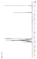
- FIG. 1 is a 1 H-NMR spectrum diagram of a compound 2-11 of the present invention.
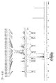
- FIG. 1 is a 1 H-NMR spectrum of a compound (7-13) of the present invention.
- the charge transport material of the present invention has a structure represented by the following general formula (1), and has 6 to 19 monocyclic aromatic rings (the aromatic ring is a carbon atom or a nitrogen atom) , Having a ring member of 6) (hereinafter, also referred to as a compound represented by the general formula (1)).
- General formula (1) Although the charge transport material of the present invention has such a structure, it is not bound by any theory, but by introducing an electron withdrawing group, the electron affinity is increased and a low driving voltage of the device can be achieved. Estimated. Further, by having such a configuration, the durability of the element is improved, although it is not limited to any theory. Therefore, the organic electroluminescent element using the charge transport material of the present invention is excellent in driving voltage and durability.
- the charge transport material represented by the general formula (1) can be preferably used for organic electronic elements such as electrophotography, organic transistors, organic photoelectric conversion elements (for energy conversion, sensor applications, etc.), and organic electroluminescence elements.
- the organic electroluminescence device is particularly preferably used.
- the charge transport material of the present invention can also be used for a thin film containing the compound represented by the general formula (1).
- the thin film can be formed using the composition by a dry film forming method such as a vapor deposition method or a sputtering method, or a wet film forming method such as a transfer method or a printing method.
- the thickness of the thin film may be any thickness depending on the application, but is preferably 0.1 nm to 1 mm, more preferably 0.5 nm to 1 ⁇ m, still more preferably 1 nm to 200 nm, and particularly preferably 1 nm to 100 nm. is there.
- the hydrogen atom in the description of the general formula (1) includes an isotope (deuterium atom and the like), and the atoms constituting the substituent further include the isotope.
- the substituent when referred to as “substituent”, the substituent may be substituted.
- the term “alkyl group” in the present invention includes an alkyl group substituted with a fluorine atom (for example, trifluoromethyl group) and an alkyl group substituted with an aryl group (for example, triphenylmethyl group).
- alkyl group having 1 to 6 carbon atoms it means that all groups including substituted ones have 1 to 6 carbon atoms.
- the charge transport material of the present invention relates to a structure represented by the general formula (1).
- R 111 to R 128 represent a hydrogen atom or a substituent. At least one of R 111 to R 122 is a cyano group.
- Examples of the substituent include a cyano group, an alkyl group having 1 to 10 carbon atoms, a halogen atom, and an aryl group having 6 to 30 carbon atoms.
- a methyl group, an ethyl group, an isopropyl group, an n-propyl group, a t-butyl group, a s-butyl group, and an n-butyl group are preferable, and a methyl group, an ethyl group, an isopropyl group, and a t-butyl group are preferable. More preferred are a methyl group and a t-butyl group, and a methyl group is particularly preferred.
- the halogen atom a fluorine atom is preferable.
- the aryl group having 6 to 30 carbon atoms is preferably an aryl group that is unsubstituted or substituted with a cyano group, and as a further condition, a chain aryl group (one benzene ring is substituted with 3 or more benzene rings). More preferred).
- the substituent is preferably a cyano group, an alkyl group or an aryl group, more preferably a cyano group or an aryl group.
- the T 1 energy in the film state of the compound represented by the general formula (1) is preferably 56 kcal / mol or more and 80 kcal / mol or less, more preferably 57 kcal / mol or more and 70 kcal / mol or less, More preferably, it is 58 kcal / mol or more and 66 kcal / mol or less.
- the T 1 energy is preferably in the above range.
- the T 1 energy can be determined from the short wavelength end of a phosphorescence emission spectrum of a thin film of material. For example, a material is deposited on a cleaned quartz glass substrate to a thickness of about 50 nm by vacuum deposition, and the phosphorescence emission spectrum of the thin film is measured at F-7000 Hitachi Spectrofluorimeter (Hitachi High Technologies) under liquid nitrogen temperature. Use to measure. T 1 energy can be obtained by converting the rising wavelength on the short wavelength side of the obtained emission spectrum into energy units.
- the molecular weight of the compound represented by the general formula (1) is preferably 1000 or less, more preferably 500 to 1000, and particularly preferably 600 to 900. . By setting the molecular weight within this range, a material having good film quality and excellent sublimation purification / deposition suitability can be obtained.
- the molecular weight of the compound represented by the general formula (1) is preferably 600 to 1000 from the viewpoint of deposition suitability.
- the glass transition temperature (Tg) of the compound represented by the general formula (1) is 80 ° C. or higher and 400 ° C. or lower (from the viewpoint of stably operating the organic electroluminescence device against heat generated during high temperature driving or driving the device) Or not detected), more preferably 100 ° C. or higher and 400 ° C. or lower (or not detected), and even more preferably 110 ° C. or higher and 400 ° C. or lower (or not detected).
- the purity of the compound represented by the general formula (1) is high.
- the purity can be measured by, for example, high performance liquid chromatography (HPLC), and the area ratio of the compound represented by the general formula (1) when detected with a light absorption intensity of 254 nm is preferably 99.00% or more, and more It is preferably 99.50% or more, particularly preferably 99.90% or more, and most preferably 99.9% or more.
- a material in which part or all of the hydrogen atoms of the compound represented by the general formula (1) are substituted with deuterium atoms is also preferably charged. It can be used as a transport material.
- the compound represented by the general formula (1) may belong to two or more of the following general formulas (1A-1) to (1A-20).
- the compound represented by the general formula (1) can be synthesized by combining the method described in JP-A-2007-266598 and other known reactions. After synthesis, it is preferable to purify by sublimation purification after purification by column chromatography, recrystallization or the like. By sublimation purification, not only can organic impurities be separated, but inorganic salts and residual solvents can be effectively removed.
- the organic electroluminescent element of the present invention has a substrate, a pair of electrodes including an anode and a cathode disposed on the substrate, and an organic layer disposed between the electrodes, and the organic layer emits phosphorescence. It contains the material and the charge transport material of the present invention, that is, the compound represented by the general formula (1).
- R 111 to R 128 each represent a hydrogen atom or a substituent. At least one of R 111 to R 122 is a cyano group, provided that each of the three consecutive benzene rings has a cyano group. The benzene ring having a cyano group is not substituted with three or more benzene rings.
- the structure of the organic electroluminescent element of the present invention is not particularly limited.
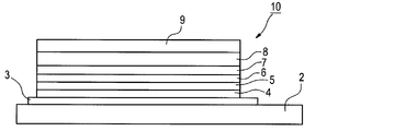
- FIG. 1 an example of a structure of the organic electroluminescent element of this invention is shown. 1 has an organic layer on a substrate 2 between a pair of electrodes (anode 3 and cathode 9).
- the element configuration, the substrate, the cathode, and the anode of the organic electroluminescence element are described in detail in, for example, Japanese Patent Application Laid-Open No. 2008-270736, and the matters described in the publication can be applied to the present invention.
- the preferable aspect of the organic electroluminescent element of this invention is demonstrated in detail in order of a board
- the organic electroluminescent element of the present invention has a substrate.
- the substrate used in the present invention is preferably a substrate that does not scatter or attenuate light emitted from the organic layer.
- the organic electroluminescent element of the present invention is disposed on the substrate and has a pair of electrodes including an anode and a cathode.
- a pair of electrodes including an anode and a cathode.
- at least one of the pair of electrodes, the anode and the cathode is preferably transparent or translucent.
- the anode usually only needs to have a function as an electrode for supplying holes to the organic layer, and there is no particular limitation on the shape, structure, size, etc., depending on the use and purpose of the light-emitting element, It can select suitably from well-known electrode materials.
- the anode is usually provided as a transparent anode.
- the cathode usually has a function as an electrode for injecting electrons into the organic layer, and there is no particular limitation on the shape, structure, size, etc., and it is known depending on the use and purpose of the light-emitting element.
- the electrode material can be selected as appropriate.
- the organic electroluminescent element of the present invention has an organic layer disposed between the electrodes, and the organic layer includes a phosphorescent material and a compound represented by the general formula (1).
- the organic layer includes a phosphorescent material and a compound represented by the general formula (1).
- the organic layer is formed on the entire surface or one surface of the transparent electrode or the semitransparent electrode.
- the organic layer is formed on the entire surface or one surface of the transparent electrode or the semitransparent electrode.
- the configuration of the organic layer, the method for forming the organic layer, preferred embodiments of the layers constituting the organic layer, and materials used for the layers will be described in order.
- the organic layer preferably includes a charge transport layer.
- the charge transport layer is a layer in which charge transfer occurs when a voltage is applied to the organic electroluminescent element. Specific examples include a hole injection layer, a hole transport layer, an electron block layer, a light emitting layer, a hole block layer, an electron transport layer, and an electron injection layer. A hole injection layer, a hole transport layer, an electron blocking layer, or a light emitting layer is preferable. If the charge transport layer formed by the coating method is a hole injection layer, a hole transport layer, an electron blocking layer, or a light emitting layer, it is possible to manufacture an organic electroluminescent element with low cost and high efficiency.
- the charge transport layer is more preferably a hole injection layer, a hole transport layer, or an electron block layer.
- the organic electroluminescent element of the present invention preferably has a light emitting layer containing the phosphorescent material and another organic layer, and the light emitting layer contains the compound represented by the general formula (1). Furthermore, in the organic electroluminescent element of the present invention, it is more preferable that the organic layer has a light emitting layer containing the phosphorescent material and another organic layer. However, in the organic electroluminescent element of the present invention, even when the organic layer has a light emitting layer and other organic layers, the layers do not necessarily have to be clearly distinguished.
- the organic layer contains a phosphorescent material and a compound represented by the general formula (1).
- the said organic layer has the light emitting layer containing the said phosphorescence-emitting material, and another organic layer, and the said light emitting layer contains the compound represented by the said General formula (1).
- the compound represented by the general formula (1) is used as a host material of the light emitting layer (hereinafter also referred to as a host compound).
- the compound represented by the general formula (1) is not limited in its application, and may be contained in any layer in the organic layer between the cathode and the anode of the organic electroluminescence device.
- the introduction layer of the compound represented by the general formula (1) is preferably contained in one or more of the light emitting layer, the layer between the light emitting layer and the cathode, and the layer between the light emitting layer and the anode.
- the compound represented by the general formula (1) is added to the light emitting layer, the organic layer adjacent to the light emitting layer between the light emitting layer and the cathode (the cathode side layer adjacent to the light emitting layer), and the light emitting layer side.
- the compound represented by the general formula (1) may be contained in both the light emitting layer and the cathode side layer adjacent to the light emitting layer.
- the compound represented by the general formula (1) is contained in the light emitting layer as a host material of the light emitting layer.
- the compound represented by the general formula (1) is 0.1 to 99 mass with respect to the total mass of the light emitting layer. %, Preferably 1 to 97% by mass, more preferably 10 to 96% by mass.
- the LUMO level is preferably in the range of ⁇ 1.90 eV or more and less than ⁇ 1.20 eV from the viewpoint of lowering the voltage and light emission efficiency. More preferably, the range is from ⁇ 1.80 eV to less than ⁇ 1.30 eV, and even more preferably from ⁇ 1.70 eV to less than ⁇ 1.40 eV. This is because the electron injection property from the electron transport layer to the light emitting layer is improved and the driving voltage is lowered.
- the specific LUMO level (lowest orbital energy) of the compound represented by the general formula (1) described in this specification is B3LYP / 6-31G (d) // B3LYP / 6-31G (d ) Is the value obtained by performing quantum chemical calculations at the level. Even with the same electron-withdrawing group, the degree of increasing the LUMO level varies depending on the substitution position.
- the LUMO level described above includes that the light emitting layer includes a partial structure represented by the following general formula (1A) as a compound having the structure represented by the general formula (1) as a host material of the light emitting layer. It is more preferable from the viewpoint of realizing a range of -1.90 eV or more and less than -1.20 eV.
- partial structures represented by the general formula (1) partial structures represented by the following general formulas (1A-1) to (1A-20), which are more preferable partial structures, are shown below.
- the invention is not limited to the following specific examples.
- the partial structure represented by the following general formula (1A-1) is ⁇ 1.51 eV
- the partial structure represented by (1A-3) is -1.58 eV
- the partial structure represented by the following general formula (1A-5) is -1.56 eV
- the partial structure represented is ⁇ 1.54 eV
- the partial structure represented by the following general formula (1A-7) is ⁇ 1.76 eV.
- the partial structure represented by the following general formula (1A-11) is ⁇ 1.87 eV
- the partial structure represented by the following general formula (1A-12) is ⁇ 1.85 eV
- the following general formula (1A- The partial structure represented by 13) is -1.73 eV
- the partial structure represented by the following general formula (1A-14) is -1.75 eV
- the partial structure is -1.91 eV
- the partial structure represented by the following general formula (1A-18) is -1.79 eV
- the partial structure represented by the following general formula (1A-19) is -1.
- the partial structure represented by the following general formula (1A-20) is -2.01 eV.
- the maximum light emission wavelength (hereinafter also referred to as emission peak wavelength) of the light emitting material is preferably 400 to 700 nm, and 470 to 650 nm. Is more preferably 490 to 620 nm, and most preferably 500 to 610 nm.
- the organic layer includes a light emitting layer containing the phosphorescent material and another organic layer, and the other organic layer disposed between the light emitting layer and the cathode is represented by the general formula (1). It is also preferable to contain a compound having a structure. Among them, the organic layer has an electron transport layer or a hole blocking layer (more preferably, a hole blocking layer), and the electron transport layer or the hole blocking layer is represented by the general formula (1). It is more preferable to contain.
- the compound represented by the general formula (1) is contained in a layer other than the light emitting layer, it is preferably contained in an amount of 70 to 100% by mass, based on the total mass of the layer other than the light emitting layer, and 80 to 100% by mass. % Is more preferable.
- the LUMO level is preferably in the range of ⁇ 2.10 eV or more and less than ⁇ 1.50 eV, preferably ⁇ 2.00 eV or more and less than ⁇ 1.55 eV. Is more preferable, and a range of ⁇ 1.90 eV or more and less than ⁇ 1.60 eV is even more preferable. This is because the electron injecting property from the cathode to the electron transporting layer is improved and the electron injecting property to the light emitting layer is improved.
- the other organic layer disposed between the light emitting layer and the cathode includes a partial structure represented by the general formula (1A) as a compound having a structure represented by the general formula (1). Is preferable from the viewpoint of realizing the above-mentioned LUMO level of ⁇ 2.10 eV or more and less than ⁇ 1.50 eV.
- another organic layer disposed between the light emitting layer and the cathode is represented by the general formula (1).
- the present invention is not limited to the following specific examples.
- positioned between the said light emitting layer and the said cathode is represented by the said partial structure group (1A) as a compound of the structure represented by the said General formula (1). It is also preferable to contain a compound having a partial structure.
- These organic layers may be provided in a plurality of layers, and when a plurality of layers are provided, they may be formed of the same material or different materials for each layer.
- each organic layer is formed by a dry film forming method such as a vapor deposition method or a sputtering method, a wet film forming method such as a transfer method, a printing method, a spin coating method, or a bar coating method (solution coating method). Any of these can be suitably formed.
- the organic layer disposed between the pair of electrodes includes at least one layer formed by vapor deposition of a composition containing the compound represented by the general formula (1). Is preferred.
- the light emitting layer receives holes from the anode, hole injection layer or hole transport layer and receives electrons from the cathode, electron injection layer or electron transport layer when an electric field is applied, and provides a field for recombination of holes and electrons. And a layer having a function of emitting light.
- the light emitting layer in the present invention is not necessarily limited to light emission by such a mechanism.
- the light emitting layer in the organic electroluminescent element of the present invention preferably contains at least one phosphorescent material.
- the light emitting layer in the organic electroluminescent device of the present invention may be composed only of the light emitting material, or may be a mixed layer of a host material and the light emitting material.
- the kind of the light emitting material may be one kind or two kinds or more.
- the host material is preferably a charge transport material.
- the host material may be one kind or two or more kinds, and examples thereof include a configuration in which an electron transporting host material and a hole transporting host material are mixed.
- the light emitting layer may include a material that does not have charge transporting properties and does not emit light.
- the light emitting layer may be a single layer or a multilayer of two or more layers, and each layer may contain the same light emitting material or host material, or each layer may contain a different material. When there are a plurality of light emitting layers, each of the light emitting layers may emit light with different emission colors.
- the thickness of the light emitting layer is not particularly limited, but is usually preferably 2 nm to 500 nm, and more preferably 3 nm to 200 nm, and more preferably 5 nm to 100 nm from the viewpoint of external quantum efficiency. More preferably.
- the light emitting layer contains a compound represented by the general formula (1), and the host material of the light emitting layer is represented by the general formula (1). It is a more preferable embodiment to use a compound.
- the host material is a compound mainly responsible for charge injection and transport in the light emitting layer, and is a compound that itself does not substantially emit light.
- substantially does not emit light means that the amount of light emitted from the compound that does not substantially emit light is preferably 5% or less, more preferably 3% or less of the total amount of light emitted from the entire device. Preferably it says 1% or less.
- the host material other than the light emitting material and the compound represented by the general formula (1) will be described in order.
- the compound represented by the said General formula (1) may be used other than the said light emitting layer in the organic electroluminescent element of this invention.
- Luminescent material As the light emitting material in the present invention, any of phosphorescent light emitting materials, fluorescent light emitting materials and the like can be used.
- the light emitting layer in the present invention can contain two or more kinds of light emitting materials in order to improve the color purity and broaden the light emission wavelength region. At least one of the light emitting materials is preferably a phosphorescent light emitting material.
- a fluorescent light-emitting material or a phosphorescent light-emitting material different from the phosphorescent light-emitting material contained in the light-emitting layer can be used as the light-emitting material.
- Examples of phosphorescent light-emitting materials that can be used in the present invention include US Pat. / 19373A2, JP-A No. 2001-247859, JP-A No. 2002-302671, JP-A No. 2002-117978, JP-A No. 2003-133074, JP-A No. 2002-1235076, JP-A No. 2003-123684, JP-A No. 2002-170684, EP No. 121157, JP-A No.
- luminescent materials include iridium (Ir) complexes, platinum (Pt) complexes, Cu complexes, and Re complexes.
- iridium (Ir) complex W complexes, Rh complexes, Ru complexes, Pd complexes, Os complexes, Eu complexes, Tb complexes, Gd complexes, Dy complexes, and Ce complexes.
- an iridium (Ir) complex a platinum (Pt) complex, or a Re complex.
- at least one coordination mode of a metal-carbon bond, a metal-nitrogen bond, a metal-oxygen bond, or a metal-sulfur bond is used.
- An iridium (Ir) complex, a platinum (Pt) complex, or a Re complex is preferable.
- iridium (Ir) complex and platinum (Pt) complex are particularly preferable, and iridium (Ir) complex is most preferable from the viewpoint of luminous efficiency, driving durability, chromaticity and the like.
- Z 1 and Z 2 each independently represents a carbon atom or a nitrogen atom.
- a 1 represents an atomic group that forms a 5- or 6-membered heterocycle with Z 1 and a nitrogen atom.
- B 1 represents an atomic group that forms a 5- or 6-membered ring with Z 2 and a carbon atom.
- Z 1 and Z 2 each independently represents a carbon atom or a nitrogen atom.
- (XY) represents a monoanionic bidentate ligand.
- n E1 represents an integer of 1 to 3.
- Z 1 and Z 2 are preferably carbon atoms.
- n E1 is preferably 2 or 3, in which case there are two or three ligands containing Z 1 , Z 2 , A 1 , B 1, which are the same as each other May be different.
- Examples of the 5- or 6-membered heterocycle containing A 1 , Z 1 and a nitrogen atom include a pyridine ring, pyrimidine ring, pyrazine ring, triazine ring, imidazole ring, pyrazole ring, oxazole ring, thiazole ring, triazole ring, oxadiazole Ring, thiadiazole ring and the like.
- the 5- or 6-membered heterocycle formed by A 1 , Z 1 and a nitrogen atom may have a substituent.
- Examples of the 5- or 6-membered ring formed by B 1 , Z 2 and a carbon atom include a benzene ring, a pyridine ring, a pyrimidine ring, a pyrazine ring, a pyridazine ring, a triazine ring, an imidazole ring, a pyrazole ring, an oxazole ring, a thiazole ring, Examples include a triazole ring, an oxadiazole ring, a thiadiazole ring, a thiophene ring, a furan ring, and a pyrrole ring.
- the 5- or 6-membered ring formed by B 1 , Z 2 and a carbon atom may have a substituent.
- the substituents may be linked to form a ring.
- the ring formed include an unsaturated 4- to 7-membered ring, a benzene ring, a pyridine ring, a pyrazine ring, a pyridazine ring, a pyrimidine ring, an imidazole ring, Examples thereof include an oxazole ring, a thiazole ring, a pyrazole ring, a thiophene ring, and a furan ring.
- These formed rings may have a substituent, and may further form a ring via a substituent on the formed ring.
- a 5- or 6-membered heterocyclic substituent formed by A 1 , Z 1 and a nitrogen atom, and a 5- or 6-membered ring substituent formed by B 1 , Z 2 and a carbon atom may be linked to form a condensed ring similar to that described above.
- a ring may be further formed through a substituent on the formed ring.
- Substituent group A An alkyl group (preferably having 1 to 30 carbon atoms, more preferably 1 to 20 carbon atoms, particularly preferably 1 to 10 carbon atoms, such as methyl, ethyl, isopropyl, t-butyl, n-octyl, n-decyl, n-hexadecyl, cyclopropyl, cyclopentyl, cyclohexyl, etc.), alkenyl groups (preferably having 2 to 30 carbon atoms, more preferably 2 to 20 carbon atoms, particularly preferably 2 to 10 carbon atoms, such as vinyl , Allyl, 2-butenyl, 3-pentenyl, etc.), alkynyl group (preferably having 2 to 30 carbon atoms, more preferably 2 to 20 carbon atoms, particularly preferably 2 to 10 carbon atoms such as propargyl , 3-pentynyl, etc.), aryl groups (preferably having 6 to 30 carbon atom
- Particularly preferably 0 to 10 carbon atoms such as amino, methylamino, dimethylamino, diethylamino, dibenzylamino, diphenylamino, ditolylamino, etc.
- an alkoxy group preferably having 1 to 30 carbon atoms, Preferably it has 1 to 20 carbon atoms, particularly preferably 1 to 10 carbon atoms, and examples thereof include methoxy, ethoxy, butoxy, 2-ethylhexyloxy, etc.
- an aryloxy group preferably having 6 to 30 carbon atoms, More preferably, it has 6 to 20 carbon atoms, particularly preferably 6 to 12 carbon atoms.
- heterocyclic oxy group preferably having 1 to 30 carbon atoms, more preferably 1 to 20 carbon atoms, and particularly preferably 1 to 12 carbon atoms.
- a heterocyclic oxy group preferably having 1 to 30 carbon atoms, more preferably 1 to 20 carbon atoms, and particularly preferably 1 to 12 carbon atoms.
- an acyl group preferably having 2 to 30 carbon atoms, more preferably 2 to 20 carbon atoms, and particularly preferably 2 to 12 carbon atoms.
- Benzoyl, formyl, pivaloyl, etc. an alkoxycarbonyl group (preferably having 2 to 30 carbon atoms, more preferably 2 to 20 carbon atoms, particularly preferably 2 to 12 carbon atoms such as methoxycarbonyl, ethoxy Carbonyl, etc.), an aryloxycarbonyl group (preferably having a carbon number)
- the number of carbon atoms is 7 to 30, more preferably 7 to 20, and particularly preferably 7 to 12, and examples thereof include phenyloxycarbonyl.
- An acyloxy group (preferably having 2 to 30 carbon atoms, more preferably 2 to 20 carbon atoms, particularly preferably 2 to 10 carbon atoms, such as acetoxy, benzoyloxy, etc.), an acylamino group (preferably 2-30 carbon atoms, more preferably 2-20 carbon atoms, particularly preferably 2-10 carbon atoms, and examples thereof include acetylamino, benzoylamino and the like, and alkoxycarbonylamino groups (preferably having 2-2 carbon atoms).
- an aryloxycarbonylamino group preferably having 7 to 30 carbon atoms, more preferably 7 to 20 carbon atoms, particularly preferably 7 to 12 carbon atoms, for example phenyloxycarbonyl And sulfonylamino groups (preferably having 1 to 30 carbon atoms, more preferably 1 to 20 carbon atoms, particularly preferably 1 to 12 carbon atoms, such as methanesulfonylamino and benzenesulfonylamino).
- an aryloxycarbonylamino group preferably having 7 to 30 carbon atoms, more preferably 7 to 20 carbon atoms, particularly preferably 7 to 12 carbon atoms, for example phenyloxycarbonyl And sulfonylamino groups (preferably having 1 to 30 carbon atoms, more preferably 1 to 20 carbon atoms, particularly preferably 1 to 12 carbon atoms, such as methanesulfonylamino and benzenesulfonylamino).
- a sulfamoyl group (preferably having 0 to 30 carbon atoms, more preferably 0 to 20 carbon atoms, particularly preferably 0 to 12 carbon atoms, such as sulfamoyl, methylsulfamoyl, dimethylsulfamoyl, phenyl Sulfamoyl, etc.), carbamoyl groups (preferably having 1 to 30 carbon atoms, more preferably 1 to 20 carbon atoms, particularly preferably 1 to 12 carbon atoms, such as carbamoyl, methylcarbamoyl, diethylcarbamoyl, Phenylcarbamoyl etc.), alkylthio group ( Preferably, it has 1 to 30 carbon atoms, more preferably 1 to 20 carbon atoms, particularly preferably 1 to 12 carbon atoms, such as methylthio, ethylthio, etc.), an arylthio group (preferably 6 to 30 carbon atoms).
- Rufinyl group (preferably having 1 to 30 carbon atoms, more preferably 1 to 20 carbon atoms, particularly preferably 1 to 12 carbon atoms, and examples thereof include methanesulfinyl and benzenesulfinyl. ), A ureido group (preferably having 1 to 30 carbon atoms, more preferably 1 to 20 carbon atoms, particularly preferably 1 to 12 carbon atoms, such as ureido, methylureido, phenylureido, etc.), phosphoric acid An amide group (preferably having 1 to 30 carbon atoms, more preferably 1 to 20 carbon atoms, particularly preferably 1 to 12 carbon atoms, such as diethyl phosphoric acid amide and phenyl phosphoric acid amide), a hydroxy group , Mercapto group, halogen atom (eg fluorine atom, chlorine atom, bromine atom, iodine atom), cyano group, sulfo group, carb
- Is for example, a nitrogen atom, oxygen atom, sulfur atom, phosphorus atom, silicon atom, selenium atom, tellurium atom, specifically pyridyl, pyrazinyl, pyrimidyl, pyridazinyl, pyrrolyl, pyrazolyl, triazolyl, imidazolyl, oxazolyl, thiazolyl, And isoxazolyl, isothiazolyl, quinolyl, furyl, thienyl, selenophenyl, tellurophenyl, piperidyl, piperidino, morpholino, pyrrolidyl, pyrrolidino, benzoxazolyl, benzoimidazolyl, benzothiazolyl, carbazolyl group, azepinyl group, silolyl group and the like.
- a silyl group (preferably having 3 to 40 carbon atoms, more preferably 3 to 30 carbon atoms, particularly preferably 3 to 24 carbon atoms, and examples thereof include trimethylsilyl and triphenylsilyl).
- a aryloxy group (preferably having 3 to 40 carbon atoms, more preferably 3 to 30 carbon atoms, particularly preferably 3 to 24 carbon atoms, such as trimethylsilyloxy, triphenylsilyloxy, etc.), phosphoryl group (for example, A diphenylphosphoryl group, a dimethylphosphoryl group, etc.).
- These substituents may be further substituted, and examples of the further substituent include a group selected from the substituent group A described above.
- the substituent substituted by the substituent may be further substituted, and examples of the further substituent include a group selected from the substituent group A described above.
- the substituent substituted by the substituent substituted by the substituent may be further substituted, and examples of the further substituent include a group selected from the substituent group A described above.
- Rx, Ry and Rz each independently represents a hydrogen atom or a substituent.
- substituent include a substituent selected from the substituent group A.
- Rx and Rz are preferably each independently an alkyl group, a perfluoroalkyl group, or an aryl group.
- Ry is preferably any one of a hydrogen atom, an alkyl group, a perfluoroalkyl group, a fluorine atom, a cyano group, and an aryl group.
- a plurality of Rx and Ry existing in one ligand may be the same or different.
- Ry may be bonded to each other to form a ring.
- Rx are not bonded to each other.
- Ligands having these ligands can be synthesized in the same manner as in known synthesis examples by using corresponding ligand precursors.
- a preferred embodiment of the iridium (Ir) complex represented by the general formula (E-1) is an iridium (Ir) complex represented by the following general formula (E-2).
- a E1 to A E8 each independently represents a nitrogen atom or C—R E.
- R E represents a hydrogen atom or a substituent.
- substituent those exemplified as the substituent group A can be applied.
- R E may be connected to each other to form a ring. Examples of the ring formed include the same ring as the condensed ring described in the general formula (E-1).
- (X-Y) and n E2 is (X-Y) in Formula (E1) have the same meanings as and n E1, preferred ranges are also the same.
- n E2 is 2 or 3
- there are two or three ligands containing A E1 to A E8, and these ligands may be the same or different.
- a more preferred form of the compound represented by the general formula (E-2) is a compound represented by the following general formula (E-3).
- R T1 , R T2 , R T3 , R T4 , R T5 , R T6, and R T7 have the same meaning as R E.
- A represents CR ′′ ′′ or a nitrogen atom, and R ′′ ′′ has the same meaning as RE.
- R T1 to R T7 and R ′′ ′′ may be bonded to any two adjacent to each other to form a condensed 4- to 7-membered ring.
- a fused 4- to 7-membered ring may further have a substituent represented by the substituent group A.
- (XY) and n E3 have the same meanings as (XY) and n E1 in formula (E-1), and the preferred ranges are also the same.
- n E3 is 2 or 3
- the ligands may be the same as or different from each other.
- the preferable range of A and R T1 to R T7 varies depending on the emission color required according to the application. In the following, description will be given by dividing into three regions of blue to light blue, green to yellow, yellow orange to red as target emission colors. However, it is not limited to these descriptions.
- R T1 to R T4 , R T7 , A (CR ′′ ′′ or a nitrogen atom), (XY) and n E4 in the general formula (E-4) are R T1 to R T1 in the general formula (E-3). It is synonymous with R T4 , R T7 , A, (XY) and n E3 .
- R 1 ′ to R 4 ′ have the same meaning as R E.
- R T1 to R T4 , R T7 , R 1 ′ to R 4 ′ and R ′′ ′′ may be bonded to each other to form a condensed 4- to 7-membered ring.
- the 7-membered ring is cycloalkene, cyclocarbadiene, aryl, or heteroaryl, and the fused 4- to 7-membered ring may further have a substituent represented by Substituent Group A.
- n E4 is 2 or 3
- R 1 ′ to R 4 ′ are preferably a hydrogen atom, a fluorine atom, an alkyl group, or an aryl group. Further, it is preferable that A represents CR ′′ ′′, and 0 to 3 of R T1 to R T4 , R T7 and R ′′ ′′ are an alkyl group or a phenyl group, and the rest are all hydrogen atoms.
- R T2 to R T6 , A (CR ′′ ′′ or nitrogen atom), (XY) and n E5 in the general formula (E-5) are R T2 to R T6 in the general formula (E-3), Synonymous with A, (XY) and n E3 .
- R 5 ′ to R 8 ′ have the same meanings as R 1 ′ to R 4 ′ in formula (E-4).
- R T2 to R T6 , R 5 ′ to R 8 ′, and R ′′ ′′ may be bonded to each other to form a condensed 4- to 7-membered ring.
- the ring is a cycloalkene, cyclocarbadiene, aryl or heteroaryl, and the condensed 4- to 7-membered ring may further have a substituent represented by the substituent group A.
- n E5 is 2 or 3
- the preferred range for R 5 ′ to R 8 ′ is the same as the preferred range for R 1 ′ to R 4 ′ in formula (E-4).
- A represents CR ′′ ′′, and among R T2 to R T6 , R ′′ ′′, and R 5 ′ to R 8 ′, 0 to 3 are alkyl groups or phenyl groups, and the rest are all hydrogen atoms. Is preferred.
- R T1 to R T5 , A (CR ′′ ′′ or nitrogen atom), (XY) and n E6 in the general formula (E-6) are R T1 to R T5 in the general formula (E-3), Synonymous with A, (XY) and n E3 .
- R 9 ′ to R 12 ′ have the same meanings as R 1 ′ to R 4 ′ in formula (E-4).
- R T1 to R T5 , R 9 ′ to R 12 ′, and R ′′ ′′ may be bonded to each other to form a condensed 4- to 7-membered ring.
- the ring is a cycloalkene, cyclocarbadiene, aryl or heteroaryl, and the condensed 4- to 7-membered ring may further have a substituent represented by the substituent group A.
- n E6 is 2 or 3
- the preferred range for R 9 ′ to R 12 ′ is the same as the preferred range for R 1 ′ to R 4 ′ in formula (E-4).
- A represents CR ′′ ′′, and among R T1 to R T5 , R ′′ ′′, and R 9 ′ to R 12 ′, 0 to 3 are alkyl groups or phenyl groups, and the rest are all hydrogen atoms. Is preferred.
- R T1 , R T2 , R T3 , R T4 , R T5 , R T6 , R T7 , R ′′ ′′, (XY) and n E3 are represented by the general formula (E ⁇ It is synonymous with R T1 , R T2 , R T3 , R T4 , R T5 , R T6 , R T7 , R ′′ ′′, (XY) and n E3 in 3 ).
- R T1 to R T7 and R ′′ ′′ may be bonded to any two adjacent to each other to form a condensed 4- to 7-membered ring.
- a fused 4- to 7-membered ring may further have a substituent represented by the substituent group A.
- n E7 is 2 or 3
- the ligands may be the same or different from each other.
- R T1 , R T2 , R T3 , R T4 , R T5 , R T6 , R T7 , R ′′ ′′ may be a hydrogen atom, a fluorine atom, an alkyl group, an aryl group, a heteroaryl group, or a cyano group preferable.
- n E7 is preferably 3, and the general formula (E-7) is preferably a compound represented by the general formula (E-7-1).
- R T1 , R T2 , R T3 , R T4 , R T5 , R T6 , R T7 , R ′′ ′′ are R T1 in the general formula (E-7), R T2 , R T3 , R T4 , R T5 , R T6 , R T7 , R ′′ ′′ have the same meanings and preferred ranges.
- R T8 to R T15 are synonymous with R T1 , R T2 , R T3 , R T4 , R T5 , R T6 , R T7 , R ′′ ′′ and the preferred ranges are also the same, but R T1 , R T2 , A phenylpyridine ligand containing R T3 , R T4 , R T5 , R T6 , R T7 , R ′′ ′′ and a phenylpyridine ligand containing R T8 to R T15 are different from each other.
- R T1 , R T2 , R T3 , R T4 , R T5 , R T6 , R T7 , R ′′ ′′ are hydrogen atoms, A fluorine atom, an alkyl group, and a cyano group are more preferable, and 1 to 3 of R T1 , R T5 , R T4 , and R ′′ ′′ are more preferably an alkyl group.
- R T8 to R T11 are more preferably a hydrogen atom or an alkyl group.
- R T12 to R T15 are more preferably a hydrogen atom, an alkyl group, a cyano group, or an aryl group.
- the substitution position of the alkyl group, cyano group or aryl group is preferably R T13 or R T14 .
- the aryl group may further have a substituent, and may form a condensed ring through the substituent.
- R T1 , R T2 , R T3 , R T4 , R T5 , R T6 , R T7 , R ′′ ′′ are hydrogen atoms, It is more preferably an alkyl group, and more preferably 1 to 3 of R T1 , R T5 , R T4 and R ′′ ′′ are alkyl groups. It is more preferable that at least one of R T8 to R T11 is an aryl group, and it is more preferable that any one of R T9 and R T10 is an aryl group and the remaining is a hydrogen atom or an alkyl group.
- the aryl group may further have a substituent, and may form a condensed ring through the substituent.
- the general formula (E-7-1) preferably has a partial structure represented by the general formula (E-7-2) in the general formula (E-7-1).
- effects such as low voltage and high durability may be noticeable depending on the combination with the host material.
- any one of R T16 to R T28 is preferably bonded to a part of general formula (E-7-1) via a single bond or an aryl group,
- R T13 or R T14 When it is desired to obtain a light emission color close to, it is more preferable to bond with R T13 or R T14 , and further preferable to bond with R T13 .
- R T9 or R T10 When it is desired to obtain a light emission color close to yellow, it is more preferable to bond with R T9 or R T10 .
- X is preferably —O—, —S—, —NR T24 —, —CR T25 R T26 —, and more preferably —O—, —S—.
- X When X is —O— or —S—, it is preferably bonded to a part of formula (E-7-1) through a single bond at the position of R T16 , and X is —NR T24 — In this case, it is preferable to bond to a part of the general formula (E-7-1) through a single bond at the position of R T18 or R T24 , and when X is —CR T25 R T26 —, R T17 It is preferable to bond to a part of the general formula (E-7-1) through a single bond at the position.
- R T1 , R T2 , R T3 , R T4 , R T5 , R T6 , R T7 , A (CR ′′ ′′ or nitrogen atom), (XY), n E8 Is synonymous with R T1 , R T2 , R T3 , R T4 , R T5 , R T6 , R T7 , A, (XY), and n E3 in the general formula (E-3).
- R T1 and R T5 to R T7 are more preferably a hydrogen atom, an alkyl group, or an aryl group.
- R T2 to R T4 are preferably a hydrogen atom, a fluorine atom, or a cyano group.
- R ′′ ′′ of CR ′′ ′′ is preferably a fluorine atom or a cyano group, or a nitrogen atom.
- n E8 is preferably 2 or 3.
- (XY) has the same meaning as (XY) in formula (E-1), and the preferred range is also the same.
- R T29 to R T34 , (XY), and n E8 have the same meanings as R T1 to R T6 (XY) and n E3 in the general formula (E-3).
- R T35 represents a substituent, and examples of the substituent include the substituent group B.
- R T29 to R T35 may combine any two adjacent to each other to form a condensed 4- to 7-membered ring, and the fused 4- to 7-membered ring is a cycloalkene, cyclocarbadiene, aryl or heteroaryl
- the condensed 4- to 7-membered ring may further have a substituent represented by the substituent group A.
- n E7 is 2 or 3
- the ligands may be the same or different from each other.
- R T29 to R T34 are preferably a hydrogen atom, an alkyl group, an aryl group, or a cyano group.
- R T35 is preferably an alkyl group or an aryl group.
- R T35 is preferably linked to R T29 to form a ring, and R T35 and R T29 are more preferably bonded via an aryl group, resulting in the formation of a nitrogen-containing 6-membered ring.
- the aryl group linked to R T29 may further have a substituent, and is more preferably substituted with an alkyl group from the viewpoint of durability.
- the compounds exemplified as the compound represented by the general formula (E-1) can be synthesized by the method described in JP2009-99783A, various methods described in US Pat. No. 7,279,232 and the like. After synthesis, it is preferable to purify by sublimation purification after purification by column chromatography, recrystallization or the like. By sublimation purification, not only can organic impurities be separated, but inorganic salts and residual solvents can be effectively removed.
- the compound represented by the general formula (E-1) is preferably contained in the light emitting layer, but its use is not limited, and may be further contained in any layer in the organic layer. .
- the compound represented by the general formula (E-1) in the light emitting layer is generally contained in the light emitting layer in an amount of 0.1% by mass to 50% by mass with respect to the total mass of the compound forming the light emitting layer.
- the content is preferably 0.2% by mass to 50% by mass, more preferably 0.3% by mass to 40% by mass, and more preferably 0.4% by mass to 30%. More preferably, it is contained in an amount of 0.5% by mass to 20% by mass.
- platinum (Pt) complex examples include compounds described in [0143] to [0152], [0157] to [0158], and [0162] to [0168] of JP-A No. 2005-310733, Compounds described in [0065] to [0083] of 2006-256999, compounds described in [0065] to [0090] of JP-A-2006-93542, and [0063] to [0063] of JP-A-2007-73491 Compounds described in [0071], compounds described in [0079] to [0083] of JP-A-2007-324309, compounds described in [0065] to [0090] of JP-A-2006-93542, JP-A Compounds described in [0055] to [0071] of 2007-96255, [0043] of JP-A-2006-313796 [0046] and the like.
- the platinum (Pt) complex that can be used as the phosphorescent material is preferably a platinum (Pt) complex represented by the following general formula (C-1).
- Q 1 , Q 2 , Q 3 and Q 4 each independently represent a ligand coordinated to platinum (Pt).
- L 1 , L 2 and L 3 are each independently a single bond or a divalent group. Represents a linking group.
- Q 1 , Q 2 , Q 3 and Q 4 each independently represent a ligand coordinated to platinum (Pt).
- the bond between Q 1 , Q 2 , Q 3 and Q 4 and platinum (Pt) may be any of a covalent bond, an ionic bond, a coordinate bond, and the like.
- a carbon atom, a nitrogen atom, an oxygen atom, a sulfur atom, and a phosphorus atom are preferable, Q ⁇ 1 >, Q ⁇ 2 >, Q ⁇ 3 > Of the atoms bonded to platinum (Pt) in Q 4 , at least one is preferably a carbon atom, more preferably two are carbon atoms, two are carbon atoms, and two are nitrogen atoms. Is particularly preferred.
- Q 1 , Q 2 , Q 3, and Q 4 bonded to platinum (Pt) by a carbon atom may be an anionic ligand or a neutral ligand, and the anionic ligand is a vinyl group.
- Ligand, aromatic hydrocarbon ring ligand eg benzene ligand, naphthalene ligand, anthracene ligand, phenanthrene ligand, etc.
- heterocyclic ligand eg furan ligand, thiophene coordination
- the groups represented by Q 1 , Q 2 , Q 3 and Q 4 may have a substituent, and as the substituent, those exemplified as the substituent group A can be appropriately applied. Moreover, substituents may be connected to each other (when Q 3 and Q 4 are connected, a platinum (Pt) complex of a cyclic tetradentate ligand is formed).
- the group represented by Q 1 , Q 2 , Q 3 and Q 4 is preferably an aromatic hydrocarbon ring ligand bonded to platinum (Pt) by a carbon atom, and an aromatic bonded to platinum (Pt) by a carbon atom.
- L 1 , L 2 and L 3 represent a single bond or a divalent linking group.
- Divalent linking groups represented by L 1 , L 2 and L 3 include alkylene groups (methylene, ethylene, propylene, etc.), arylene groups (phenylene, naphthalenediyl), heteroarylene groups (pyridinediyl, thiophenediyl, etc.) ), Imino group (—NR—) (eg phenylimino group), oxy group (—O—), thio group (—S—), phosphinidene group (—PR—) (eg phenylphosphinidene group), silylene group (—SiRR′—) (dimethylsilylene group, diphenylsilylene group, etc.), or a combination thereof.
- alkylene groups methylene, ethylene, propylene, etc.
- arylene groups phenylene, naphthalenediyl
- heteroarylene groups pyridinedi
- R and R ′ each independently include an alkyl group, an aryl group, and the like. These linking groups may further have a substituent.
- a single bond as L 1, L 2 and L 3
- an alkylene group, an arylene group, heteroarylene group, an imino group, an oxy group, a thio group be a silylene group More preferably a single bond, an alkylene group, an arylene group or an imino group, still more preferably a single bond, an alkylene group or an arylene group, still more preferably a single bond, a methylene group or a phenylene group, still more preferably.
- Single bond, disubstituted methylene group more preferably single bond, dimethylmethylene group, diethylmethylene group, diisobutylmethylene group, dibenzylmethylene group, ethylmethylmethylene group, methylpropylmethylene group, isobutylmethylmethylene group, diphenyl Methylene group, methylphenylmethylene group, cyclohexanediyl group, cyclope An tandiyl group, a fluorenediyl group, and a fluoromethylmethylene group.
- L 1 is particularly preferably a dimethylmethylene group, a diphenylmethylene group, or a cyclohexanediyl group, and most preferably a dimethylmethylene group.
- L 2 and L 3 are most preferably a single bond.
- platinum (Pt) complexes represented by the general formula (C-1) a platinum (Pt) complex represented by the following general formula (C-2) is more preferable.
- L 21 represents a single bond or a divalent linking group.
- a 21 and A 22 each independently represents a carbon atom or a nitrogen atom.
- Z 21 and Z 22 each independently represent a nitrogen-containing aromatic heterocyclic ring.
- Z 23 and Z 24 each independently represents a benzene ring or an aromatic heterocycle.
- L 21 has the same meaning as L 1 in formula (C-1), and the preferred range is also the same.
- a 21 and A 22 each independently represent a carbon atom or a nitrogen atom. Of A 21, A 22, Preferably, at least one is a carbon atom, it A 21, A 22 are both carbon atoms are preferred from the standpoint of emission quantum yield stability aspects and complexes of the complex .
- Z 21 and Z 22 each independently represent a nitrogen-containing aromatic heterocycle.
- the nitrogen-containing aromatic heterocycle represented by Z 21 and Z 22 include a pyridine ring, pyrimidine ring, pyrazine ring, triazine ring, imidazole ring, pyrazole ring, oxazole ring, thiazole ring, triazole ring, oxadiazole ring, Examples include thiadiazole rings.
- the ring represented by Z 21 and Z 22 is preferably a pyridine ring, a pyrazine ring, an imidazole ring or a pyrazole ring, more preferably a pyridine ring.
- Z 23 and Z 24 each independently represent a benzene ring or an aromatic heterocycle.
- the nitrogen-containing aromatic heterocycle represented by Z 23 and Z 24 include pyridine ring, pyrimidine ring, pyrazine ring, pyridazine ring, triazine ring, imidazole ring, pyrazole ring, oxazole ring, thiazole ring, triazole ring, oxadi Examples include an azole ring, a thiadiazole ring, a thiophene ring, and a furan ring.
- the ring represented by Z 23 and Z 24 is preferably a benzene ring, a pyridine ring, a pyrazine ring, an imidazole ring, a pyrazole ring, or a thiophene ring. More preferred are a benzene ring, a pyridine ring and a pyrazole ring, and still more preferred are a benzene ring and a pyridine ring.
- platinum (Pt) complexes represented by the general formula (C-2) one of the more preferred embodiments is a platinum (Pt) complex represented by the following general formula (C-4).
- a 401 to A 414 each independently represents C—R or a nitrogen atom.
- R represents a hydrogen atom or a substituent.
- L 41 represents a single bond or a divalent linking group.
- a 401 to A 414 each independently represents C—R or a nitrogen atom.
- R represents a hydrogen atom or a substituent.
- substituent represented by R those exemplified as the substituent group A can be applied.
- a 401 to A 406 are preferably C—R, and Rs may be connected to each other to form a ring.
- R in A 402 and A 405 is preferably a hydrogen atom, an alkyl group, an aryl group, an amino group, an alkoxy group, an aryloxy group, a fluorine atom, or a cyano group.
- R in A 401 , A 403 , A 404 and A 406 is preferably a hydrogen atom, an alkyl group, an aryl group, an amino group, an alkoxy group, an aryloxy group, a fluorine atom or a cyano group, more preferably a hydrogen atom or amino Group, an alkoxy group, an aryloxy group and a fluorine atom, and particularly preferably a hydrogen atom.
- L 41 has the same meaning as L 1 in formula (C-1), and the preferred range is also the same.
- the number of N is preferably 0 to 2, and more preferably 0 to 1.
- either A 408 or A 412 is preferably a nitrogen atom, and more preferably both A 408 and A 412 are nitrogen atoms.
- platinum (Pt) complexes represented by the general formula (C-2) one of the more preferred embodiments is a platinum (Pt) complex represented by the following general formula (C-5).
- a 501 to A 512 each independently represents C—R or a nitrogen atom, R represents a hydrogen atom or a substituent, and L 51 represents a single bond or a divalent linkage. Represents a group.
- a 501 to A 506 and L 51 have the same meanings as A 401 to A 406 and L 41 in formula (C-4), and preferred ranges thereof are also the same.
- R represents a hydrogen atom or a substituent.
- substituent represented by R those exemplified as the substituent group A can be applied.
- platinum (Pt) complexes represented by the general formula (C-1) another more preferable embodiment is a platinum (Pt) complex represented by the following general formula (C-6).
- L 61 represents a single bond or a divalent linking group.
- a 61 independently represents a carbon atom or a nitrogen atom.
- Z 61 and Z 62 each independently represent a nitrogen-containing aromatic heterocycle.
- Z 63 independently represents a benzene ring or an aromatic heterocycle, and
- Y is an anionic acyclic ligand bonded to platinum (Pt).
- L 61 has the same meaning as L 1 in formula (C-1), and the preferred range is also the same.
- a 61 represents a carbon atom or a nitrogen atom. In view of the stability of the complex and the light emission quantum yield of the complex, A 61 is preferably a carbon atom.
- Z 61 and Z 62 are synonymous with Z 21 and Z 22 in the general formula (C-2), respectively, and preferred ranges thereof are also the same.
- Z 63 has the same meaning as Z 23 in formula (C-2), and the preferred range is also the same.
- Y is an anionic acyclic ligand that binds to platinum (Pt).
- An acyclic ligand is one in which atoms bonded to platinum (Pt) do not form a ring in the state of a ligand.
- a carbon atom, a nitrogen atom, an oxygen atom, and a sulfur atom are preferable, a nitrogen atom and an oxygen atom are more preferable, and an oxygen atom is the most preferable.
- a vinyl ligand is mentioned as Y couple
- Examples of Y bonded to platinum (Pt) with a nitrogen atom include an amino ligand and an imino ligand.
- Examples of Y bonded to platinum (Pt) with an oxygen atom include an alkoxy ligand, an aryloxy ligand, a heteroaryloxy ligand, an acyloxy ligand, a silyloxy ligand, a carboxyl ligand, and a phosphate group. Examples thereof include ligands and sulfonic acid ligands.
- Examples of Y bonded to platinum (Pt) with a sulfur atom include alkyl mercapto ligands, aryl mercapto ligands, heteroaryl mercapto ligands, and thiocarboxylic acid ligands.
- the ligand represented by Y may have a substituent, and those listed as the substituent group A can be appropriately applied as the substituent. Moreover, substituents may be connected to each other.
- the ligand represented by Y is preferably a ligand bonded to platinum (Pt) with an oxygen atom, and more preferably an acyloxy ligand, an alkyloxy ligand, an aryloxy ligand, a heteroaryloxy A ligand and a silyloxy ligand are preferable, and an acyloxy ligand is more preferable.
- platinum (Pt) complexes represented by the general formula (C-6) one of the more preferred embodiments is a platinum (Pt) complex represented by the following general formula (C-7).
- a 701 to A 710 each independently represents C—R or a nitrogen atom, R represents a hydrogen atom or a substituent, L 71 represents a single bond or a divalent linking group, Y represents (It is an anionic acyclic ligand that binds to platinum (Pt).)
- L 71 has the same meaning as L 61 in formula (C-6), and the preferred range is also the same.
- a 701 to A 710 have the same meanings as A 401 to A 410 in formula (C-4), and the preferred ranges are also the same.
- Y has the same meaning as Y in formula (C-6), and the preferred range is also the same.
- platinum (Pt) complex represented by the general formula (C-1) include [0143] to [0152], [0157] to [0158], and [0162] to JP-A-2005-310733.
- a Compounds described in [0090], compounds described in [0055] to [0071] of JP-A-2007-96255, JP-A-2006-31379 No. [0043] - [0046] can be mentioned publications, other include platinum (Pt) complex exemplified below.
- the platinum (Pt) complex compound represented by the general formula (C-1) is described in, for example, Journal of Organic Chemistry 53,786, (1988), G.A. R. Newkome et al. ), Page 789, method described in left column 53 to right column 7, line 790, method described in left column 18 to 38, method 790, method described in right column 19 to 30 and The combination, Chemische Berichte 113, 2749 (1980), H.C. Lexy et al.), Page 2752, lines 26 to 35, and the like.
- a ligand or a dissociated product thereof and a metal compound are mixed with a solvent (for example, a halogen solvent, an alcohol solvent, an ether solvent, an ester solvent, a ketone solvent, a nitrile solvent, an amide solvent, a sulfone solvent,
- a solvent for example, a halogen solvent, an alcohol solvent, an ether solvent, an ester solvent, a ketone solvent, a nitrile solvent, an amide solvent, a sulfone solvent
- a base inorganic and organic bases such as sodium methoxide, t-butoxypotassium, triethylamine, potassium carbonate, etc.
- a base inorganic and organic bases such as sodium methoxide, t-butoxypotassium, triethylamine, potassium carbonate, etc.
- the content of the compound represented by formula (C-1) in the light emitting layer of the present invention is preferably 1 to 30% by mass, more preferably 3 to 25% by mass in the light emitting layer. More preferably, it is 20 mass%.
- the type of the fluorescent material is not particularly limited.
- the thickness of the light emitting layer is not particularly limited, but is usually preferably 2 nm to 500 nm, and more preferably 5 nm to 200 nm, and more preferably 10 nm to 100 nm, from the viewpoint of external quantum efficiency. More preferably.
- the light emitting layer in the organic electroluminescent element of the present invention may be composed only of a light emitting material, or may be a mixed layer of a host material and a light emitting material.
- the kind of the light emitting material may be one kind or two or more kinds.
- the host material is preferably a charge transport material.
- the host material may be one kind or two or more kinds, and examples thereof include a configuration in which an electron transporting host material and a hole transporting host material are mixed.
- the light emitting layer may contain a material that does not have charge transporting properties and does not emit light.
- the light emitting layer may be a single layer or a multilayer of two or more layers, and each layer may contain the same light emitting material or host material, or each layer may contain a different material. When there are a plurality of light emitting layers, each of the light emitting layers may emit light with different emission colors.
- the host material is a compound mainly responsible for charge injection and transport in the light emitting layer, and itself is a compound that does not substantially emit light.
- “substantially does not emit light” means that the amount of light emitted from the compound that does not substantially emit light is preferably 5% or less, more preferably 3% or less of the total amount of light emitted from the entire device. Preferably it says 1% or less.
- a compound represented by the general formula (1) can be used as the host material.
- Examples of other host materials that can be used in the organic electroluminescence device of the present invention include the following compounds. Pyrrole, indole, carbazole, azaindole, azacarbazole, triazole, oxazole, oxadiazole, pyrazole, imidazole, thiophene, benzothiophene, dibenzothiophene, furan, benzofuran, dibenzofuran, polyarylalkane, pyrazoline, pyrazolone, phenylenediamine, aryl Amines, amino-substituted chalcones, styrylanthracenes, fluorenones, hydrazones, stilbenes, silazanes, aromatic tertiary amine compounds, styrylamine compounds, porphyrin compounds, condensed aromatic hydrocarbon compounds (fluorene, naphthalene, phenanthrene, triphenylene, etc.) , Polys
- the host material that can be used in combination in the light emitting layer of the organic electroluminescent device of the present invention may be a hole transporting host material or an electron transporting host material.
- the triplet lowest excitation energy (T 1 energy) in the film state of the host material is preferably higher than the T 1 energy of the phosphorescent light emitting material in terms of color purity, light emission efficiency, and driving durability. It is preferable T 1 is greater 0.1eV higher than the T 1 of the phosphorescent material of the host material, more preferably at least 0.2eV higher, and further preferably more than 0.3eV large. T 1 of the a film state of the host material is a large T 1 is obtained from the phosphorescent material to the host material for thereby quench T 1 is less than the light emission of the phosphorescent material.
- the content of the host compound in the light emitting layer in the organic electroluminescent device of the present invention is not particularly limited, but is 15 mass with respect to the total compound mass forming the light emitting layer from the viewpoint of light emission efficiency and driving voltage. % Or more and 95% by mass or less is preferable.
- the light emitting layer contains a plurality of types of host compounds including the compound represented by the general formula (1)
- the compound represented by the general formula (1) is 50% by mass or more and 99% by mass or less in all the host compounds. It is preferable.
- the organic electroluminescent element of the present invention may have other layers other than the light emitting layer.
- Other organic layers other than the light emitting layer that the organic layer may have include a hole injection layer, a hole transport layer, a block layer (hole block layer, exciton block layer, electron block layer, etc.), Examples thereof include an electron transport layer.
- Examples of the specific layer configuration include the following, but the present invention is not limited to these configurations.
- the organic electroluminescent element of the present invention preferably includes (A) at least one organic layer preferably disposed between the anode and the light emitting layer.
- Examples of the organic layer (A) preferably disposed between the anode and the light emitting layer include a hole injection layer, a hole transport layer, and an electron block layer from the anode side.
- the organic electroluminescent element of the present invention preferably includes (B) at least one organic layer preferably disposed between the cathode and the light emitting layer.
- Examples of the organic layer (B) preferably disposed between the cathode and the light emitting layer include an electron injection layer, an electron transport layer, and a hole blocking layer from the cathode side.
- an example of a preferred embodiment of the organic electroluminescent element of the present invention is the embodiment described in FIG. 1, and as the organic layer, a hole injection layer 4, a hole transport layer 5, In this embodiment, the light emitting layer 6, the hole blocking layer 7, and the electron transport layer 8 are laminated in this order.
- the organic layer a hole injection layer 4, a hole transport layer 5, In this embodiment, the light emitting layer 6, the hole blocking layer 7, and the electron transport layer 8 are laminated in this order.
- other layers other than the light emitting layer which may be included in the organic electroluminescent element of the present invention will be described.
- the hole injection layer and the hole transport layer are layers having a function of receiving holes from the anode or the anode side and transporting them to the cathode side.
- the matters described in paragraph numbers [0165] to [0167] of JP-A-2008-270736 can be applied to the present invention.
- the material preferably used for the hole injection layer and the hole transport layer will be described.
- the organic electroluminescent element of the present invention preferably contains the following compound in the organic layer between the light emitting layer and the anode, and more preferably in the hole injection layer. Specifically, a compound having the following structure is preferable.
- the organic electroluminescent element of the present invention preferably contains at least one compound represented by the following general formula (M-1) in the organic layer between the light emitting layer and the anode, and the hole transport layer contains It is more preferable to contain.
- Ar 1 and Ar 2 are each independently one or more selected from alkyl, aryl, heteroaryl, arylamino, alkylamino, morpholino, thiomorpholino, N, O, and S It represents a 5- or 6-membered heterocycloalkyl or cycloalkyl containing a hetero atom, and may further have a substituent Z.
- Ar 1 and Ar 2 may be bonded to each other by a single bond, alkylene, or alkenylene (with or without a condensed ring) to form a condensed 5- to 9-membered ring.
- Ar 3 represents alkyl, aryl, heteroaryl, or arylamino, and may further have a substituent Z.
- Z is independently a halogen atom, -R “, -OR", -N (R ") 2 , -SR", -C (O) R “, -C (O) OR", -C (O) N (R ") 2, -CN , -NO 2, -SO 2, -SOR", - SO 2 R “, or -SO 3 R” represents, R "are each independently a hydrogen atom, an alkyl group, A perhaloalkyl group, an alkenyl group, an alkynyl group, a heteroalkyl group, an aryl group or a heteroaryl group is represented.
- p is an integer of 1 to 4, and when p is 2 or more, Ar 1 and Ar 2 may be the same or different.
- Another preferred embodiment of the compound represented by the general formula (M-1) is a case represented by the following general formula (M-3).
- R S1 to R S5 are each independently an alkyl group, cycloalkyl group, alkenyl group, alkynyl group, —CN, perfluoroalkyl group, trifluorovinyl group, —CO 2 R, —C (O) R, —NR 2 , —NO 2 , —OR, a halogen atom, an aryl group or a heteroaryl group, which may further have a substituent Z.
- Each R independently represents a hydrogen atom, an alkyl group, a perhaloalkyl group, an alkenyl group, an alkynyl group, a heteroalkyl group, an aryl group or a heteroaryl group.
- R S1 to R S5 When a plurality of R S1 to R S5 are present, they may be bonded to each other to form a ring, and may further have a substituent Z.
- a represents an integer of 0 to 4, and when a plurality of R S1 are present, they may be the same or different and may be bonded to each other to form a ring.
- b to e each independently represent an integer of 0 to 5, and when there are a plurality of R S2 to R S5 , respectively, they may be the same or different, and any two may be bonded to form a ring.
- q is an integer of 1 to 5, and when q is 2 or more, a plurality of R S1 may be the same or different, and may be bonded to each other to form a ring.
- the alkyl group may have a substituent, may be saturated or unsaturated, and examples of the group that may be substituted include the above-described substituent Z.
- the alkyl group represented by R S1 to R S5 is preferably an alkyl group having 1 to 8 carbon atoms in total, more preferably an alkyl group having 1 to 6 carbon atoms in total, such as a methyl group or an ethyl group. , I-propyl group, cyclohexyl group, t-butyl group and the like.
- the cycloalkyl group may have a substituent, may be saturated or unsaturated, and examples of the group that may be substituted include the above-described substituent Z.
- the cycloalkyl group represented by R S1 to R S5 is preferably a cycloalkyl group having 4 to 7 ring members, more preferably a cycloalkyl group having 5 to 6 carbon atoms in total, such as a cyclopentyl group or cyclohexyl group. Groups and the like.
- the alkenyl group represented by R S1 to R S5 preferably has 2 to 30 carbon atoms, more preferably 2 to 20 carbon atoms, and particularly preferably 2 to 10 carbon atoms.
- vinyl, allyl, 1-propenyl Examples include 1-isopropenyl, 1-butenyl, 2-butenyl, 3-pentenyl and the like.
- the alkynyl group represented by R S1 to R S5 preferably has 2 to 30 carbon atoms, more preferably 2 to 20 carbon atoms, and particularly preferably 2 to 10 carbon atoms.
- Examples of the perfluoroalkyl group represented by R S1 to R S5 include those in which all the hydrogen atoms of the aforementioned alkyl group are replaced with fluorine atoms.
- the aryl group represented by R S1 to R S5 is preferably a substituted or unsubstituted aryl group having 6 to 30 carbon atoms, such as a phenyl group, a tolyl group, a biphenyl group, and a terphenyl group.
- the heteroaryl group represented by R S1 to R S5 is preferably a heteroaryl group having 5 to 8 carbon atoms, more preferably a 5- or 6-membered substituted or unsubstituted heteroaryl group,
- R S1 to R S5 are preferably a hydrogen atom, an alkyl group, a cyano group, a trifluoromethyl group, a perfluoroalkyl group, a dialkylamino group, a fluoro group, an aryl group, or a heteroaryl group, and more preferably a hydrogen atom, an alkyl group Group, cyano group, trifluoromethyl group, fluoro group and aryl group, more preferably a hydrogen atom, an alkyl group and an aryl group.
- substituent Z an alkyl group, an alkoxy group, a fluoro group, a cyano group, and a dialkylamino group are preferable, and a hydrogen atom and an alkyl group are more preferable.
- R S1 to R S5 may be bonded to each other to form a condensed 4- to 7-membered ring, and the condensed 4- to 7-membered ring is cycloalkyl, aryl, or heteroaryl;
- the 7-membered ring may further have a substituent Z.
- the definition and preferred range of cycloalkyl, aryl, and heteroaryl formed are the same as the cycloalkyl group, aryl group, and heteroaryl group defined by R S1 to R S5 .
- the compound represented by the general formula (M-1) is preferably contained in an amount of 50 to 100% by mass, The content is preferably 100% by mass, and particularly preferably 95 to 100% by mass.
- each layer contains the above-mentioned range.
- the compound represented by the general formula (M-1) may contain only one kind in any organic layer, and the compound represented by the plurality of general formulas (M-1) You may contain in combination.
- the thickness of the hole transport layer containing the compound represented by the general formula (M-1) is preferably 1 nm to 500 nm, more preferably 3 nm to 200 nm, and more preferably 5 nm to 100 nm. Further preferred.
- the hole transport layer is preferably provided in contact with the light emitting layer.
- the hole transport layer may have a single layer structure composed of one or more of the above-described materials, or may have a multilayer structure composed of a plurality of layers having the same composition or different compositions.
- the lowest excited triplet (T 1 ) energy in the film state of the compound represented by the general formula (M-1) is preferably 2.52 eV (58 kcal / mol) or more and 3.47 eV (80 kcal / mol) or less.
- EV (57 kcal / mol) or more and 3.25 eV (75 kcal / mol) or less, more preferably 2.52 eV (58 kcal / mol) or more and 3.04 eV (70 kcal / mol) or less.
- the hydrogen atom constituting the general formula (M-1) includes hydrogen isotopes (such as deuterium atoms). In this case, all hydrogen atoms in the compound may be replaced with hydrogen isotopes, or a mixture in which a part is a compound containing hydrogen isotopes may be used.
- the compound represented by the general formula (M-1) can be synthesized by combining various known synthesis methods.
- carbazole compounds are synthesized by dehydroaromatization after the Athercorp rearrangement reaction of a condensate of an aryl hydrazine and a cyclohexane derivative (LF Tieze, by Th. Eicher, translated by Takano, Ogasawara, Precision organic synthesis, page 339 (published by Nankodo).
- LF Tieze by Th. Eicher, translated by Takano, Ogasawara, Precision organic synthesis, page 339 (published by Nankodo).
- LF Tieze by Th. Eicher
- Takano, Ogasawara, Precision organic synthesis page 339 (published by Nankodo).
- Tetrahedron Letters 39: 617 (1998), 39: 2367 (1998) and 40: 6393 (1999) and the like Tetrahedron Letters 39: 617 (1998), 39: 2367 (1998) and 40
- the compound represented by the general formula (M-1) of the present invention is preferably formed into a thin layer by a vacuum deposition process, but a wet process such as solution coating can also be suitably used.
- the molecular weight of the compound is preferably 2000 or less, more preferably 1200 or less, and particularly preferably 800 or less from the viewpoints of deposition suitability and solubility. Also, from the viewpoint of vapor deposition suitability, if the molecular weight is too small, the vapor pressure becomes small, the change from the gas phase to the solid phase does not occur, and it is difficult to form an organic layer. Particularly preferred.
- the hole transport material among the compounds represented by the general formula (M-1), a compound having the following structure is preferable.
- the hole injection layer preferably contains an electron accepting dopant.
- an electron-accepting dopant may be any organic material or inorganic material as long as it can extract electrons from the doped material and generate radical cations.
- TCNQ tetracyanoquinodimethane
- F 4 -TCNQ tetrafluorotetracyanoquinodimethane
- molybdenum oxide and the like.
- the electron-accepting dopant in the hole injection layer is preferably contained in an amount of 0.01% by mass to 50% by mass, and preferably 0.1% by mass to 40% by mass with respect to the total mass of the compound forming the hole injection layer. %, More preferably 0.2% by mass to 30% by mass.
- the electron blocking layer is a layer having a function of preventing electrons transported from the cathode side to the light emitting layer from passing through to the anode side.
- an electron blocking layer can be provided as an organic layer adjacent to the light emitting layer on the anode side.
- the organic compound constituting the electron blocking layer for example, those mentioned as the hole transport material described above can be applied.
- the thickness of the electron blocking layer is preferably 1 nm to 500 nm, more preferably 3 nm to 100 nm, and even more preferably 5 nm to 50 nm.
- the electron blocking layer may have a single layer structure composed of one or more of the above-described materials, or may have a multilayer structure composed of a plurality of layers having the same composition or different compositions.
- the material used for the electron blocking layer is preferably higher than the T 1 energy of the phosphorescent material in terms of color purity, luminous efficiency, and driving durability. It is preferable T 1 is greater than 0.1eV than T 1 of the phosphorescent material in the film state of the material used for the electron blocking layer, it is more preferably at least 0.2eV higher, and further preferably more than 0.3eV large.
- the electron injection layer and the electron transport layer are layers having a function of receiving electrons from the cathode or the cathode side and transporting them to the anode side.
- the electron injection material and the electron transport material used for these layers may be a low molecular compound or a high molecular compound.
- the electron transport material the compound represented by the general formula (1) can be used, and a preferable embodiment thereof is a case where the compound represented by the general formula (1) is contained in a layer other than the light emitting layer. As explained.
- electron transport materials include pyridine derivatives, quinoline derivatives, pyrimidine derivatives, pyrazine derivatives, phthalazine derivatives, phenanthroline derivatives, triazine derivatives, triazole derivatives, oxazole derivatives, oxadiazole derivatives, imidazole derivatives, fluorenone derivatives, anthraquinodimethane.
- anthrone derivatives diphenylquinone derivatives, thiopyran dioxide derivatives, carbodiimide derivatives, fluorenylidenemethane derivatives, distyrylpyrazine derivatives, aromatic ring tetracarboxylic anhydrides such as naphthalene and perylene, phthalocyanine derivatives, 8-quinolinol derivatives Represented by metal complexes, metal phthalocyanines, various metal complexes represented by metal complexes with benzoxazole and benzothiazole ligands, and siloles Organosilane derivatives, a layer containing such is preferable.
- the thicknesses of the electron injection layer and the electron transport layer are each preferably 500 nm or less from the viewpoint of lowering the driving voltage.
- the thickness of the electron transport layer is preferably 1 nm to 500 nm, more preferably 5 nm to 200 nm, and even more preferably 10 nm to 100 nm.
- the thickness of the electron injection layer is preferably from 0.1 nm to 200 nm, more preferably from 0.2 nm to 100 nm, and even more preferably from 0.5 nm to 50 nm.
- the electron injection layer and the electron transport layer may have a single layer structure composed of one or more of the above-described materials, or may have a multilayer structure composed of a plurality of layers having the same composition or different compositions.
- the electron injection layer preferably contains an electron donating dopant.
- an electron donating dopant may be any organic material or inorganic material as long as it can give electrons to the doped material and generate radical anions.
- TTF tetrathiafulvalene
- TTT dithiaimidazole compounds
- TTT tetrathianaphthacene
- bis- [1,3 diethyl-2-methyl-1,2-dihydrobenzimidazolyl] lithium, cesium and the like.
- the electron donating dopant in the electron injection layer is preferably contained in an amount of 0.01% by mass to 50% by mass, and 0.1% by mass to 40% by mass with respect to the total mass of the compound forming the electron injection layer. More preferably, the content is 0.5 to 30% by mass.
- the hole blocking layer is a layer having a function of preventing holes transported from the anode side to the light emitting layer from passing through to the cathode side.
- a hole blocking layer can be provided as an organic layer adjacent to the light emitting layer on the cathode side.
- the T 1 energy in the film state of the organic compound constituting the hole blocking layer is higher than the T 1 energy of the light emitting material in order to prevent energy transfer of excitons generated in the light emitting layer and not to reduce the light emission efficiency. It is preferable.
- the organic compound constituting the hole blocking layer the compound represented by the general formula (1) can be used.
- Examples of other organic compounds constituting the hole blocking layer other than the compound represented by the general formula (1) include aluminum (III) bis (2-methyl-8-quinolinato) 4-phenylphenolate ( Aluminum complexes such as aluminum (III) bis (2-methyl-8-quinolinato) 4-phenylphenolate (abbreviated as Balq)), triazole derivatives, 2,9-dimethyl-4,7-diphenyl-1,10-phenanthroline ( And phenanthroline derivatives such as 2,9-Dimethyl-4,7-diphenyl-1,10-phenanthroline (abbreviated as BCP)) and the compounds of the present invention.
- Aluminum complexes such as aluminum (III) bis (2-methyl-8-quinolinato) 4-phenylphenolate (abbreviated as Balq)
- triazole derivatives 2,9-dimethyl-4,7-diphenyl-1,10-phenanthroline
- BCP 2,9-Dimethyl-4,7-diphenyl-1,10-phenanthroline
- the hole blocking layer is not limited to the function of actually blocking holes, and the exciton of the light emitting layer may not diffuse into the electron transport layer, or may have a function of blocking energy transfer quenching. .
- the compound of the present invention can also be preferably applied as a hole blocking layer.
- the thickness of the hole blocking layer is preferably 1 nm to 500 nm, more preferably 5 nm to 200 nm, and even more preferably 10 nm to 100 nm.
- the hole blocking layer may have a single layer structure made of one or more of the materials described above, or may have a multilayer structure made of a plurality of layers having the same composition or different compositions.
- the material used for the hole blocking layer is preferably higher than the T 1 energy of the phosphorescent light emitting material in terms of color purity, light emission efficiency, and driving durability.
- Holes T 1 of the at film state of the material used in the blocking layer is preferably greater 0.1eV higher than the T 1 of the phosphorescent material, more preferably at least 0.2eV higher, and further preferably more than 0.3eV greater .
- the organic electroluminescent element of the present invention is preferably disposed between the (B) cathode and the light emitting layer.
- a material that is particularly preferably used for the material of the organic layer a compound represented by the general formula (1) and a compound represented by the following general formula (O-1) can be given.
- the compound represented by the general formula (O-1) will be described.
- the organic electroluminescent device of the present invention preferably includes at least one organic layer between the light emitting layer and the cathode, and the organic layer contains at least one compound represented by the following general formula (O-1). It is preferable from the viewpoint of device efficiency and driving voltage.
- the general formula (O-1) will be described below.
- R O1 represents an alkyl group, an aryl group, or each independently .A O1 ⁇ A O4 representing the heteroaryl group, the C-R A or .R A representing the nitrogen atom Represents a hydrogen atom, an alkyl group, an aryl group, or a heteroaryl group, and a plurality of R A may be the same or different, L O1 represents a divalent to hexavalent linking group comprising an aryl ring or a heteroaryl ring; N O1 represents an integer of 2 to 6.
- R O1 represents an alkyl group (preferably having 1 to 8 carbon atoms), an aryl group (preferably having 6 to 30 carbon atoms), or a heteroaryl group (preferably having 4 to 12 carbon atoms). It may have a substituent selected from group A.
- R O1 is preferably an aryl group or a heteroaryl group, more preferably an aryl group.
- a preferable substituent when the aryl group of R O1 has a substituent includes an alkyl group, an aryl group or a cyano group, more preferably an alkyl group or an aryl group, and still more preferably an aryl group.
- the aryl group of R O1 When the aryl group of R O1 has a plurality of substituents, the plurality of substituents may be bonded to each other to form a 5- or 6-membered ring.
- the aryl group of R O1 is preferably a phenyl group which may have a substituent selected from the substituent group A, more preferably a phenyl group which may be substituted with an alkyl group or an aryl group, More preferred is an unsubstituted phenyl group or 2-phenylphenyl group.
- a O1 to A O4 each independently represent C—R A or a nitrogen atom.
- 0 to 2 are preferably nitrogen atoms, more preferably 0 or 1 is a nitrogen atom.
- all of A O1 ⁇ A O4 is C-R A, or A O1 be a nitrogen atom, is preferably A O2 ⁇ A O4 is C-R A, A O1 be a nitrogen atom, A O2 ⁇ More preferably, A O4 is C—R A , A O1 is a nitrogen atom, A O2 to A O4 are C—R A , and R A is all hydrogen atoms.
- R A represents a hydrogen atom, an alkyl group (preferably having a carbon number of 1 to 8), an aryl group (preferably having a carbon number of 6 to 30), or a heteroaryl group (preferably having a carbon number of 4 to 12). It may have a substituent selected from the substituent group A.
- the plurality of R A may be the same or different.
- R A is preferably a hydrogen atom or an alkyl group, more preferably a hydrogen atom.
- L O1 represents a divalent to hexavalent linking group consisting of an aryl ring (preferably having 6 to 30 carbon atoms) or a heteroaryl ring (preferably having 4 to 12 carbon atoms).
- L O1 is preferably an arylene group, heteroarylene group, aryltriyl group, or heteroaryltriyl group, more preferably a phenylene group, a biphenylene group, or a benzenetriyl group, still more preferably a biphenylene group, Or it is a benzenetriyl group.
- L O1 may have a substituent selected from the aforementioned substituent group A, and the alkyl group, aryl group, or cyano group is preferred as the substituent when it has a substituent. Specific examples of L O1 include the following.
- n O1 represents an integer of 2 to 6, preferably an integer of 2 to 4, more preferably 2 or 3. n O1 is most preferably 3 in terms of device efficiency, and most preferably 2 in terms of device durability.
- the compound represented by the general formula (O-1) is more preferably a compound represented by the following general formula (O-2).
- R O1 represents an alkyl group, an aryl group, or a heteroaryl group.
- R O2 to R O4 each independently represents a hydrogen atom, an alkyl group, an aryl group, or a heteroaryl group.
- a O1 to A O4 each independently represent C—R A or a nitrogen atom, R A represents a hydrogen atom, an alkyl group, an aryl group, or a heteroaryl group, and a plurality of R A are the same or different. May be.
- R O1 and A O1 ⁇ A O4 the general formula (O1) in the same meaning as R O1 and A O1 ⁇ A O4 of, also the same preferable ranges thereof.
- R 02 to R 04 are each independently a hydrogen atom, an alkyl group (preferably having 1 to 8 carbon atoms), an aryl group (preferably having 6 to 30 carbon atoms), or a heteroaryl group (preferably having 4 to 12 carbon atoms). These may have a substituent selected from the aforementioned substituent group A.
- R 02 to R 04 are preferably a hydrogen atom, an alkyl group, or an aryl group, more preferably a hydrogen atom or an aryl group, and most preferably a hydrogen atom.
- the compound represented by the general formula (O-1) has a glass transition temperature (Tg) of 100 ° C. from the viewpoint of stable operation at high temperature storage, stable operation against high temperature driving, and heat generation during driving. It is preferably from ⁇ 300 ° C., more preferably from 120 ° C. to 300 ° C., further preferably from 120 ° C. to 300 ° C., and still more preferably from 140 ° C. to 300 ° C.
- the compound represented by the general formula (O-1) can be synthesized by the method described in JP-A No. 2001-335776. After synthesis, purification by column chromatography, recrystallization, reprecipitation, etc., followed by purification by sublimation is preferred. Not only can organic impurities be separated by sublimation purification, but inorganic salts, residual solvents, moisture, and the like can be effectively removed.
- the compound represented by the general formula (O-1) is preferably contained in the organic layer between the light emitting layer and the cathode, but the cathode side layer adjacent to the light emitting layer is used. It is more preferable that it is contained.
- the compound represented by the general formula (O-1) is preferably contained in an amount of 70 to 100% by mass, and more preferably 85 to 100% by mass with respect to the total mass of the organic layer to be added.
- the entire organic electroluminescent element may be protected by a protective layer.
- the protective layer the matters described in JP-A-2008-270736, paragraphs [0169] to [0170] can be applied to the present invention.
- the material for the protective layer may be inorganic or organic.
- the organic electroluminescent element of the present invention may be sealed entirely using a sealing container.
- the sealing container the matters described in paragraph [0171] of JP-A-2008-270736 can be applied to the present invention.
- the organic electroluminescence device of the present invention emits light by applying a direct current (which may include an alternating current component as necessary) voltage (usually 2 to 15 volts) or a direct current between the anode and the cathode. Obtainable.
- the driving method of the organic electroluminescence device of the present invention is described in JP-A-2-148687, JP-A-6-301355, JP-A-5-290080, JP-A-7-134558, JP-A-8-234585, and JP-A-8-2441047.
- the driving methods described in each publication, Japanese Patent No. 2784615, US Pat. Nos. 5,828,429 and 6,023,308 can be applied.
- the external quantum efficiency of the organic electroluminescent element of the present invention is preferably 7% or more, more preferably 10% or more, and further preferably 12% or more.
- the value of the external quantum efficiency should be the maximum value of the external quantum efficiency when the device is driven at 20 ° C., or the value of the external quantum efficiency in the vicinity of 300 to 400 cd / m 2 when the device is driven at 20 ° C. Can do.
- the internal quantum efficiency of the organic electroluminescence device of the present invention is preferably 30% or more, more preferably 50% or more, and further preferably 70% or more.
- the internal quantum efficiency of the device is calculated by dividing the external quantum efficiency by the light extraction efficiency. In a normal organic EL element, the light extraction efficiency is about 20%.
- the organic electroluminescent element of the present invention has no limitation on the emission peak wavelength.
- the organic electroluminescence device of the present invention preferably has an emission peak wavelength of 500 to 700 nm from the viewpoint of the lowest excited triplet (T 1 ) energy of the compound represented by the general formula (1).
- the emission peak wavelength is preferably 500 to 700 nm. It is more preferably from ⁇ 650 nm, particularly preferably from 520 to 550 nm.
- the emission peak wavelength is preferably 400 to 700 nm, It is more preferably from ⁇ 650 nm, particularly preferably from 500 to 650 nm.
- the organic electroluminescent element of the present invention can be suitably used for a display element, a display, a backlight, an electrophotography, an illumination light source, a recording light source, an exposure light source, a reading light source, a sign, a signboard, an interior, or optical communication.
- a device that is driven in a region where light emission luminance is high such as a light emitting device, a lighting device, and a display device.
- the light emitting device of the present invention includes the organic electroluminescent element of the present invention. Next, the light emitting device of the present invention will be described with reference to FIG.
- the light emitting device of the present invention uses the organic electroluminescent element.
- FIG. 2 is a cross-sectional view schematically showing an example of the light emitting device of the present invention.
- the light-emitting device 20 of FIG. 2 is comprised by the board
- the organic electroluminescent device 10 is configured by sequentially laminating an anode (first electrode) 3, an organic layer 11, and a cathode (second electrode) 9 on a substrate 2.
- a protective layer 12 is laminated on the cathode 9, and a sealing container 16 is provided on the protective layer 12 with an adhesive layer 14 interposed therebetween.
- a part of each electrode 3 and 9, a partition, an insulating layer, etc. are abbreviate
- the adhesive layer 14 a photocurable adhesive such as an epoxy resin or a thermosetting adhesive can be used, and for example, a thermosetting adhesive sheet can also be used.
- the use of the light-emitting device of the present invention is not particularly limited, and for example, it can be a display device such as a television, a personal computer, a mobile phone, and electronic paper in addition to a lighting device.
- FIG. 3 is a cross-sectional view schematically showing an example of the illumination device of the present invention.
- the illumination device 40 of the present invention includes the organic EL element 10 and the light scattering member 30 described above. More specifically, the lighting device 40 is configured such that the substrate 2 of the organic EL element 10 and the light scattering member 30 are in contact with each other.
- the light scattering member 30 is not particularly limited as long as it can scatter light.
- the light scattering member 30 is a member in which fine particles 32 are dispersed on a transparent substrate 31.
- a glass substrate can be preferably cited.
- the fine particles 32 transparent resin fine particles can be preferably exemplified.
- the glass substrate and the transparent resin fine particles known ones can be used. In such an illuminating device 40, when light emitted from the organic electroluminescent element 10 is incident on the light incident surface 30A of the scattering member 30, the incident light is scattered by the light scattering member 30, and the scattered light is emitted from the light emitting surface 30B. It is emitted as illumination light.
- the display device of the present invention includes the organic electroluminescent element of the present invention.
- Examples of the display device of the present invention include a display device such as a television, a personal computer, a mobile phone, and electronic paper.
- Synthesis Example 1 The compound represented by the general formula (1) can be synthesized by combining known reactions. (Synthesis Example 1) Synthesis of compound (2-11)
- FIG. 5 shows the 1 H-NMR spectrum of the compound (7-13).
- Example 1 A glass substrate having a thickness of 0.5 mm and a 2.5 cm square ITO film (manufactured by Geomat Co., Ltd., surface resistance 10 ⁇ / ⁇ ) is placed in a cleaning container, subjected to ultrasonic cleaning in 2-propanol, and then subjected to UV-ozone treatment for 30 minutes. Went. The following organic layers were sequentially deposited on the transparent anode (ITO film) by vacuum deposition.
- ITO film transparent anode
- First layer Compound (A) below: Film thickness 10 nm
- Second layer HTL-1: film thickness 25 nm
- Third layer Compound (1-1) and GD-1 (mass ratio 90:10): film thickness 40 nm
- Fourth layer ETL-1: film thickness 40 nm
- 0.1 nm of lithium fluoride and 100 nm of metallic aluminum were vapor-deposited in this order to form a cathode.
- This laminated body is put in a glove box substituted with nitrogen gas without being exposed to the atmosphere, and sealed with a glass sealing can and an ultraviolet curable adhesive (XNR5516HV, manufactured by Nagase Ciba Co., Ltd.). The device 1 was obtained.
- Examples 2 to 11, Comparative Examples 1 to 5 In the preparation of the element 1, the compound (1-1) in the third layer was replaced with the compound represented by the general formula (1) shown in the following Table 1 and the above-mentioned comparative compounds (1) to (5). In the same manner as in the element 1, elements of the examples and comparative examples were obtained.
- Table 1 shows the results of evaluating these elements from the viewpoint of efficiency, durability, and driving voltage by the following method.
- Drive voltage Each element is caused to emit light by applying a DC voltage so that the luminance becomes 1000 cd / m 2 .
- the applied voltage at this time was used as an index for driving voltage evaluation.
- Table 1 below shows the case where the driving voltage is less than 6V, ⁇ , the case where it is 6V or more and less than 7V, ⁇ , the case where it is 7V or more and less than 8V, and the case where it is 8V or more.
- Example 12 to 14, Comparative Examples 6 to 10 In the preparation of device 1, device 9 was obtained by substituting the compounds described below. Further, the third layer compound (1-1) was the same as the device 9 except that the compound represented by the general formula (1) shown in Table 2 below and the above-mentioned comparative compounds (1) to (5) were replaced. Thus, elements of the examples and comparative examples were obtained.
- Example 15 Comparative Examples 11 to 15
- the element 15 was obtained by replacing the compound (ETL-1) in the fourth layer with the compound (1-3) of the present invention.
- each example was performed in the same manner as in the element 1 except that the compound (1-3) in the fourth layer was replaced with the compound represented by the general formula (1) shown in Table 3 below and the above-described comparative compound (5).
- the element of the comparative example was obtained.
- the light-emitting element of the present invention is designed to increase the light emission efficiency in such a case. Therefore, it can be used advantageously.
- the element of the present invention is excellent in durability and is suitable for a light emitting device, a display device, and a lighting device.
Abstract
A charge transport material, which has a structure indicated by the following formula, and which comprises a compound containing 6-19 monocyclic aromatic rings (the members of the aromatic ring are carbon atoms or nitrogen atoms, and the number of ring members is 6), has a low driving voltage and excellent durability (R111-R128 indicate hydrogen atoms or substituents thereof. At least one of R111-R122 is a cyano group. However, not all of three continuous benzene rings will each have a cyano group, and a benzene ring having a cyano group will not be substituted by three or more benzene rings).
Description
本発明は電荷輸送材料、有機電界発光素子、発光装置、表示装置および照明装置に関する。
The present invention relates to a charge transport material, an organic electroluminescent element, a light emitting device, a display device, and a lighting device.
有機電界発光素子(以下、「素子」、「有機EL素子」ともいう)は、低電圧駆動で高輝度の発光が得られることから活発に研究開発が行われている。有機電界発光素子は、一対の電極間に有機層を有し、陰極から注入された電子と陽極から注入された正孔とが有機層において再結合し、生成した励起子のエネルギーを発光に利用するものである。
Organic electroluminescent elements (hereinafter also referred to as “elements” and “organic EL elements”) are actively researched and developed because they can emit light with high luminance when driven at a low voltage. An organic electroluminescent element has an organic layer between a pair of electrodes, and electrons injected from the cathode and holes injected from the anode recombine in the organic layer, and the generated exciton energy is used for light emission. To do.
近年、燐光発光材料を用いることにより、素子の高効率化が進んでいる。更なる素子の発光効率の向上及び駆動電圧の低減のため、オルト位に置換基を有するベンゾニトリル系電荷輸送材料の使用が特許文献1に記載されている。
In recent years, the use of phosphorescent light-emitting materials has advanced the efficiency of devices. Patent Document 1 discloses the use of a benzonitrile-based charge transport material having a substituent at the ortho position for further improving the light emission efficiency of the device and reducing the driving voltage.
本発明者らが検討したところ、特許文献1に記載の従来の素子では、駆動電圧が高過ぎであり、耐久性にも問題があることが明らかになった。特に、これまでに報告されている化合物である、後述の実施例で示される比較化合物1~5などを使用した素子は、いずれも駆動電圧が高過ぎ、また耐久性が低い等の問題点があった。
As a result of studies by the present inventors, it has been clarified that in the conventional element described in Patent Document 1, the driving voltage is too high and there is a problem in durability. In particular, the devices using comparative compounds 1 to 5 shown in Examples described later, which have been reported so far, all have problems such as excessive driving voltage and low durability. there were.
すなわち、本発明の目的は、低駆動電圧であり、耐久性が良好である電荷輸送材料を提供することである。
また、本発明の別の目的は、上記電荷輸送材料を用いた有機電界発光素子を提供することである。更に、本発明の別の目的は、本発明の有機電界発光素子を含む発光装置、表示装置及び照明装置を提供することである。 That is, an object of the present invention is to provide a charge transport material having a low driving voltage and good durability.
Another object of the present invention is to provide an organic electroluminescent device using the charge transport material. Furthermore, another object of the present invention is to provide a light emitting device, a display device, and a lighting device including the organic electroluminescent element of the present invention.
本発明者らの検討によると、特定のp-ターフェニル構造を有し、単環の芳香環の個数が特許文献1に記載の化合物よりも多い化合物を電荷輸送材料として用いることで、低駆動電圧であり、耐久性が良好である有機電界発光素子が提供されることを見出した。
According to the study by the present inventors, the use of a compound having a specific p-terphenyl structure and a larger number of monocyclic aromatic rings than the compound described in Patent Document 1 as a charge transporting material enables low driving. It has been found that an organic electroluminescent device having a good voltage and durability is provided.
すなわち、本発明は下記の手段により達成することができる。
[1] 下記一般式(1)で表される構造であり、かつ、6~19個の単環のベンゼン環を含む化合物からなる電荷輸送材料。
一般式(1)

(一般式(1)中、R111~R128は水素原子または置換基を表す。R111~R122の少なくとも1個はシアノ基である。但し、連続する3個のベンゼン環のそれぞれにシアノ基を有することはなく、シアノ基を有するベンゼン環が3個以上のベンゼン環で置換されることはない。)
[2] 前記一般式(1)におけるR111~R128のうち、1または2個がシアノ基であることを特徴とする[1]に記載の電荷輸送材料。
[3] 前記一般式(1)で表される構造を有する化合物の分子量が500~1000であることを特徴とする[1]または[2]に記載の電荷輸送材料。
[4] 基板と、
該基板上に配置され、陽極及び陰極を含む一対の電極と、
該電極間に配置された有機層とを有し、
前記有機層が、燐光発光材料と[1]~[3]のいずれか一項に記載の電荷輸送材料を含有することを特徴とする有機電界発光素子。
[5] 前記有機層が、前記燐光発光材料を含む発光層を有し、該発光層が前記一般式(1)で表される構造の化合物を含有することを特徴とする[4]に記載の有機電界発光素子。
[6] 前記発光層が、前記一般式(1)で表される構造の化合物として、下記一般式(3-A)で表される部分構造で表される部分構造を含むことを特徴とする[5]に記載の有機電界発光素子。
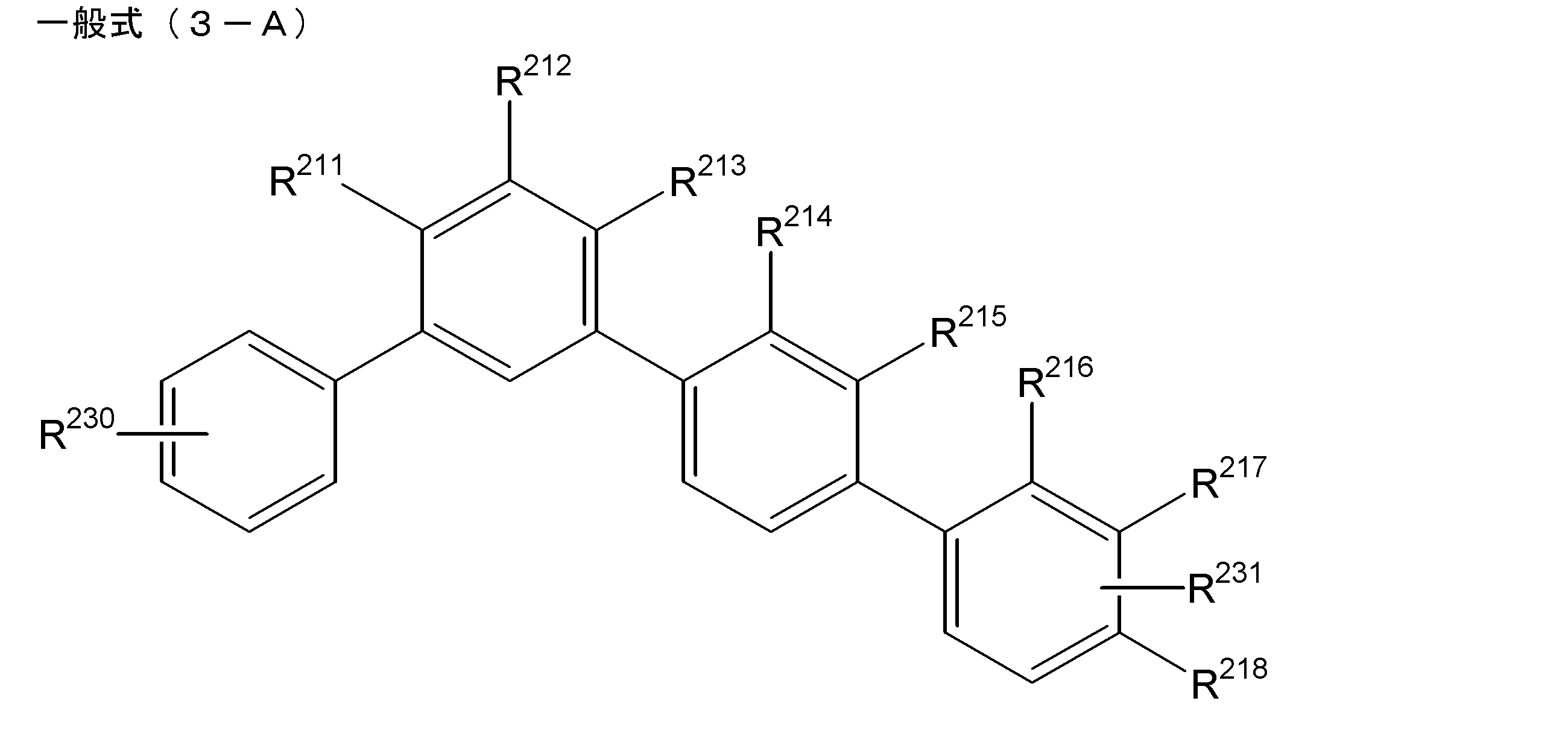
(一般式(3-A)中、R230およびR231はそれぞれ独立に水素原子またはアリール基(但し、アルキル基、ハロゲン原子、シアノ基、あるいはアリール基で置換されていてもよい。但し、置換基を含めて縮合多環構造を有さない)を表す。R230およびR231の少なくとも1個はアリール基を表す。R211~R218のうち1または2個がシアノ基を表す。但し、連続する3個のベンゼン環のそれぞれにシアノ基を有することはなく、シアノ基を有するベンゼン環が3個以上のベンゼン環で置換されることはない。R211~R218のうち、シアノ基が2個である場合は1つのベンゼン環に2個のシアノ基を有することは無い。)
[7] 前記発光層が、前記一般式(1)で表される構造の化合物として、下記部分構造群(1A)で表される部分構造を有する化合物を含有することを特徴とする[5]または[6]に記載の有機電界発光素子。

[8] 前記有機層が、前記燐光発光材料を含む発光層とその他の有機層を有し、
前記発光層と前記陰極との間に配置されたその他の有機層が、前記一般式(1)で表される構造の化合物を含有することを特徴とする[5]~[7]のいずれか一項に記載の有機電界発光素子。
[9] 前記発光層と前記陰極との間に配置されたその他の有機層が、前記一般式(1)で表される構造の化合物として、下記部分構造群(1A)で表される部分構造を有する化合物を含有することを特徴とする[8]に記載の有機電界発光素子。

[10] 前記部分構造群(1A)で表される部分構造を有する化合物において、1つのベンゼン環に3つ以上のベンゼン環が置換されていない鎖状構造であることを特徴とする[9]に記載の有機電界発光素子。
[11] 前記一般式(1)で表される構造の化合物として、部分構造群(1A-1)、(1A-2)、(1A-3)、(1A-7)のいずれかで表される部分構造を有する化合物を含有することを特徴とする[9]または[10]に記載の有機電界発光素子。
[12] 前記発光層に前記一般式(1)で表される化合物を少なくとも一種含有し、かつ、
前記発光層と陰極との間に配置されたその他の有機層に前記一般式(1)で表される化合物を少なくとも一種含有することを特徴とする[11]に記載の有機電界発光素子。
[13] 前記発光層に、前記燐光発光材料としてイリジウム(Ir)錯体を用いることを特徴とする[8]~[12]のいずれか一項に記載の有機電界発光素子。
[14] 前記発光層に、前記燐光発光材料として下記一般式(E-1)で表されるイリジウム(Ir)錯体を用いることを特徴とする[8]~[12]のいずれか一項に記載の有機電界発光素子。
一般式(E-1)
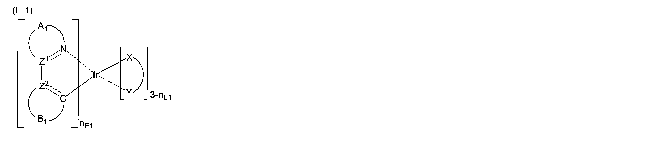
一般式(E-1)中、Z1及びZ2はそれぞれ独立に、炭素原子又は窒素原子を表す。A1はZ1と窒素原子と共に5又は6員のヘテロ環を形成する原子群を表す。B1はZ2と炭素原子と共に5又は6員環を形成する原子群を表す。Z1及びZ2はそれぞれ独立に、炭素原子又は窒素原子を表す。(X-Y)はモノアニオン性の二座配位子を表す。nE1は1~3の整数を表す。
[15] [8]~[14]のいずれか一項に記載の有機電界発光素子を含むことを特徴とする発光装置、表示装置または照明装置。 That is, the present invention can be achieved by the following means.
[1] A charge transport material having a structure represented by the following general formula (1) and comprising a compound containing 6 to 19 monocyclic benzene rings.
General formula (1)
(In the general formula (1), R 111 to R 128 each represent a hydrogen atom or a substituent. At least one of R 111 to R 122 is a cyano group, provided that each of the three consecutive benzene rings has a cyano group. The benzene ring having a cyano group is not substituted with three or more benzene rings.
[2] The charge transport material according to [1], wherein one or two of R 111 to R 128 in the general formula (1) are cyano groups.
[3] The charge transport material according to [1] or [2], wherein the compound having the structure represented by the general formula (1) has a molecular weight of 500 to 1,000.
[4] a substrate;
A pair of electrodes disposed on the substrate, including an anode and a cathode;
An organic layer disposed between the electrodes,
An organic electroluminescence device, wherein the organic layer contains a phosphorescent material and the charge transport material according to any one of [1] to [3].
[5] The organic layer has a light emitting layer containing the phosphorescent material, and the light emitting layer contains a compound having a structure represented by the general formula (1). Organic electroluminescent element.
[6] The light emitting layer includes a partial structure represented by the partial structure represented by the following general formula (3-A) as the compound having the structure represented by the general formula (1). The organic electroluminescent element as described in [5].
(In the general formula (3-A), R 230 and R 231 are each independently substituted with a hydrogen atom or an aryl group (however, an alkyl group, a halogen atom, a cyano group, or an aryl group may be substituted. And at least one of R 230 and R 231 represents an aryl group, and one or two of R 211 to R 218 represent a cyano group, provided that not to have each a cyano group three consecutive benzene rings, among .R 211 ~ R 218 does not benzene ring is substituted with three or more benzene rings having cyano group, a cyano group In the case of two, there is no two cyano groups in one benzene ring.)
[7] The light emitting layer contains a compound having a partial structure represented by the following partial structure group (1A) as a compound having a structure represented by the general formula (1) [5] Or the organic electroluminescent element as described in [6].
[8] The organic layer has a light emitting layer containing the phosphorescent material and another organic layer,
Any one of [5] to [7], wherein the other organic layer disposed between the light emitting layer and the cathode contains a compound having a structure represented by the general formula (1). The organic electroluminescent element according to one item.
[9] The partial structure represented by the following partial structure group (1A) as the compound having the structure represented by the general formula (1) as the other organic layer disposed between the light emitting layer and the cathode The organic electroluminescent element as described in [8], comprising a compound having
[10] The compound having a partial structure represented by the partial structure group (1A) is a chain structure in which three or more benzene rings are not substituted on one benzene ring [9] The organic electroluminescent element of description.
[11] The compound having the structure represented by the general formula (1) is represented by any one of the partial structure groups (1A-1), (1A-2), (1A-3), and (1A-7). The organic electroluminescent element as described in [9] or [10], comprising a compound having a partial structure.
[12] The light emitting layer contains at least one compound represented by the general formula (1), and
[11] The organic electroluminescent device as described in [11], wherein the other organic layer disposed between the light emitting layer and the cathode contains at least one compound represented by the general formula (1).
[13] The organic electroluminescent element as described in any one of [8] to [12], wherein an iridium (Ir) complex is used as the phosphorescent material in the light emitting layer.
[14] In any one of [8] to [12], an iridium (Ir) complex represented by the following general formula (E-1) is used for the phosphorescent material as the phosphorescent material. The organic electroluminescent element as described.
Formula (E-1)
In general formula (E-1), Z 1 and Z 2 each independently represents a carbon atom or a nitrogen atom. A 1 represents an atomic group that forms a 5- or 6-membered heterocycle with Z 1 and a nitrogen atom. B 1 represents an atomic group that forms a 5- or 6-membered ring with Z 2 and a carbon atom. Z 1 and Z 2 each independently represents a carbon atom or a nitrogen atom. (XY) represents a monoanionic bidentate ligand. n E1 represents an integer of 1 to 3.
[15] A light-emitting device, a display device, or a lighting device comprising the organic electroluminescent element according to any one of [8] to [14].
[1] 下記一般式(1)で表される構造であり、かつ、6~19個の単環のベンゼン環を含む化合物からなる電荷輸送材料。
一般式(1)
[2] 前記一般式(1)におけるR111~R128のうち、1または2個がシアノ基であることを特徴とする[1]に記載の電荷輸送材料。
[3] 前記一般式(1)で表される構造を有する化合物の分子量が500~1000であることを特徴とする[1]または[2]に記載の電荷輸送材料。
[4] 基板と、
該基板上に配置され、陽極及び陰極を含む一対の電極と、
該電極間に配置された有機層とを有し、
前記有機層が、燐光発光材料と[1]~[3]のいずれか一項に記載の電荷輸送材料を含有することを特徴とする有機電界発光素子。
[5] 前記有機層が、前記燐光発光材料を含む発光層を有し、該発光層が前記一般式(1)で表される構造の化合物を含有することを特徴とする[4]に記載の有機電界発光素子。
[6] 前記発光層が、前記一般式(1)で表される構造の化合物として、下記一般式(3-A)で表される部分構造で表される部分構造を含むことを特徴とする[5]に記載の有機電界発光素子。
[7] 前記発光層が、前記一般式(1)で表される構造の化合物として、下記部分構造群(1A)で表される部分構造を有する化合物を含有することを特徴とする[5]または[6]に記載の有機電界発光素子。
前記発光層と前記陰極との間に配置されたその他の有機層が、前記一般式(1)で表される構造の化合物を含有することを特徴とする[5]~[7]のいずれか一項に記載の有機電界発光素子。
[9] 前記発光層と前記陰極との間に配置されたその他の有機層が、前記一般式(1)で表される構造の化合物として、下記部分構造群(1A)で表される部分構造を有する化合物を含有することを特徴とする[8]に記載の有機電界発光素子。
[11] 前記一般式(1)で表される構造の化合物として、部分構造群(1A-1)、(1A-2)、(1A-3)、(1A-7)のいずれかで表される部分構造を有する化合物を含有することを特徴とする[9]または[10]に記載の有機電界発光素子。
[12] 前記発光層に前記一般式(1)で表される化合物を少なくとも一種含有し、かつ、
前記発光層と陰極との間に配置されたその他の有機層に前記一般式(1)で表される化合物を少なくとも一種含有することを特徴とする[11]に記載の有機電界発光素子。
[13] 前記発光層に、前記燐光発光材料としてイリジウム(Ir)錯体を用いることを特徴とする[8]~[12]のいずれか一項に記載の有機電界発光素子。
[14] 前記発光層に、前記燐光発光材料として下記一般式(E-1)で表されるイリジウム(Ir)錯体を用いることを特徴とする[8]~[12]のいずれか一項に記載の有機電界発光素子。
一般式(E-1)
[15] [8]~[14]のいずれか一項に記載の有機電界発光素子を含むことを特徴とする発光装置、表示装置または照明装置。 That is, the present invention can be achieved by the following means.
[1] A charge transport material having a structure represented by the following general formula (1) and comprising a compound containing 6 to 19 monocyclic benzene rings.
General formula (1)
[2] The charge transport material according to [1], wherein one or two of R 111 to R 128 in the general formula (1) are cyano groups.
[3] The charge transport material according to [1] or [2], wherein the compound having the structure represented by the general formula (1) has a molecular weight of 500 to 1,000.
[4] a substrate;
A pair of electrodes disposed on the substrate, including an anode and a cathode;
An organic layer disposed between the electrodes,
An organic electroluminescence device, wherein the organic layer contains a phosphorescent material and the charge transport material according to any one of [1] to [3].
[5] The organic layer has a light emitting layer containing the phosphorescent material, and the light emitting layer contains a compound having a structure represented by the general formula (1). Organic electroluminescent element.
[6] The light emitting layer includes a partial structure represented by the partial structure represented by the following general formula (3-A) as the compound having the structure represented by the general formula (1). The organic electroluminescent element as described in [5].
[7] The light emitting layer contains a compound having a partial structure represented by the following partial structure group (1A) as a compound having a structure represented by the general formula (1) [5] Or the organic electroluminescent element as described in [6].
Any one of [5] to [7], wherein the other organic layer disposed between the light emitting layer and the cathode contains a compound having a structure represented by the general formula (1). The organic electroluminescent element according to one item.
[9] The partial structure represented by the following partial structure group (1A) as the compound having the structure represented by the general formula (1) as the other organic layer disposed between the light emitting layer and the cathode The organic electroluminescent element as described in [8], comprising a compound having
[11] The compound having the structure represented by the general formula (1) is represented by any one of the partial structure groups (1A-1), (1A-2), (1A-3), and (1A-7). The organic electroluminescent element as described in [9] or [10], comprising a compound having a partial structure.
[12] The light emitting layer contains at least one compound represented by the general formula (1), and
[11] The organic electroluminescent device as described in [11], wherein the other organic layer disposed between the light emitting layer and the cathode contains at least one compound represented by the general formula (1).
[13] The organic electroluminescent element as described in any one of [8] to [12], wherein an iridium (Ir) complex is used as the phosphorescent material in the light emitting layer.
[14] In any one of [8] to [12], an iridium (Ir) complex represented by the following general formula (E-1) is used for the phosphorescent material as the phosphorescent material. The organic electroluminescent element as described.
Formula (E-1)
[15] A light-emitting device, a display device, or a lighting device comprising the organic electroluminescent element according to any one of [8] to [14].
本発明によれば、低駆動電圧であり、耐久性が良好である電荷輸送材料を提供することができる。
According to the present invention, it is possible to provide a charge transport material having a low driving voltage and good durability.
以下において、本発明の内容について詳細に説明する。以下に記載する構成要件の説明は、本発明の代表的な実施態様に基づいてなされることがあるが、本発明はそのような実施態様に限定されるものではない。尚、本願明細書において「~」とはその前後に記載される数値を下限値および上限値として含む意味で使用される。
Hereinafter, the contents of the present invention will be described in detail. The description of the constituent elements described below may be made based on typical embodiments of the present invention, but the present invention is not limited to such embodiments. In the present specification, “to” is used to mean that the numerical values described before and after it are included as a lower limit value and an upper limit value.
[電荷輸送材料]
本発明の電荷輸送材料は、下記一般式(1)で表される構造であり、かつ、6~19個の単環の芳香環(該芳香環は、環員が炭素原子または窒素原子であり、環員数が6である)を含む化合物(以下、一般式(1)で表される化合物とも言う)からなることを特徴とする。
一般式(1)
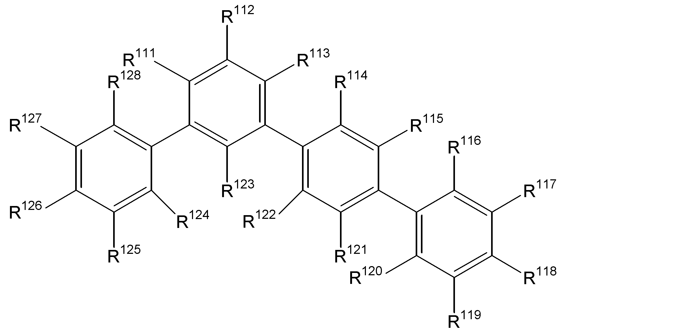
本発明の電荷輸送材料はこのような構成を有することで、いかなる理論に拘泥するものでもないが、電子求引基を導入することによって電子親和力が増大し、素子の低駆動電圧化を達成できるものと推定される。また、このような構成を有することで、いかなる理論に拘泥するものでもないが、素子の耐久性が向上する。そのため、本発明の電荷輸送材料を用いた有機電界発光素子は、駆動電圧や耐久性に優れる。
[Charge transport material]
The charge transport material of the present invention has a structure represented by the following general formula (1), and has 6 to 19 monocyclic aromatic rings (the aromatic ring is a carbon atom or a nitrogen atom) , Having a ring member of 6) (hereinafter, also referred to as a compound represented by the general formula (1)).
General formula (1)
Although the charge transport material of the present invention has such a structure, it is not bound by any theory, but by introducing an electron withdrawing group, the electron affinity is increased and a low driving voltage of the device can be achieved. Estimated. Further, by having such a configuration, the durability of the element is improved, although it is not limited to any theory. Therefore, the organic electroluminescent element using the charge transport material of the present invention is excellent in driving voltage and durability.
本発明の電荷輸送材料は、下記一般式(1)で表される構造であり、かつ、6~19個の単環の芳香環(該芳香環は、環員が炭素原子または窒素原子であり、環員数が6である)を含む化合物(以下、一般式(1)で表される化合物とも言う)からなることを特徴とする。
一般式(1)
The charge transport material of the present invention has a structure represented by the following general formula (1), and has 6 to 19 monocyclic aromatic rings (the aromatic ring is a carbon atom or a nitrogen atom) , Having a ring member of 6) (hereinafter, also referred to as a compound represented by the general formula (1)).
General formula (1)
前記一般式(1)で表される電荷輸送材料は、電子写真、有機トランジスタ、有機光電変換素子(エネルギー変換用途、センサー用途等)、有機電界発光素子等の有機エレクトロニクス素子に好ましく用いることができ、有機電界発光素子に用いるのが特に好ましい。
本発明の電荷輸送材料は、前記一般式(1)で表される化合物を含有する薄膜にも用いることができる。該薄膜は、前記組成物を用いて蒸着法やスパッタ法等の乾式製膜法、転写法、印刷法等の湿式製膜法により形成することができる。薄膜の膜厚は用途によっていかなる厚みでもよいが、好ましくは0.1nm~1mmであり、より好ましくは0.5nm~1μmであり、更に好ましくは1nm~200nmであり、特に好ましくは1nm~100nmである。 The charge transport material represented by the general formula (1) can be preferably used for organic electronic elements such as electrophotography, organic transistors, organic photoelectric conversion elements (for energy conversion, sensor applications, etc.), and organic electroluminescence elements. The organic electroluminescence device is particularly preferably used.
The charge transport material of the present invention can also be used for a thin film containing the compound represented by the general formula (1). The thin film can be formed using the composition by a dry film forming method such as a vapor deposition method or a sputtering method, or a wet film forming method such as a transfer method or a printing method. The thickness of the thin film may be any thickness depending on the application, but is preferably 0.1 nm to 1 mm, more preferably 0.5 nm to 1 μm, still more preferably 1 nm to 200 nm, and particularly preferably 1 nm to 100 nm. is there.
以下、前記一般式(1)で表される化合物からなる電荷輸送材料の好ましい範囲について説明する。
なお、本発明において、前記一般式(1)の説明における水素原子は同位体(重水素原子等)も含み、また更に置換基を構成する原子は、その同位体も含んでいることを表す。
本発明において、「置換基」というとき、その置換基は置換されていてもよい。例えば、本発明で「アルキル基」と言う時、フッ素原子で置換されたアルキル基(例えばトリフルオロメチル基)やアリール基で置換されたアルキル基(例えばトリフェニルメチル基)なども含むが、「炭素数1~6のアルキル基」と言うとき、置換されたものも含めた全ての基として炭素数が1~6であることを示す。 Hereinafter, the preferable range of the charge transport material comprising the compound represented by the general formula (1) will be described.
In the present invention, the hydrogen atom in the description of the general formula (1) includes an isotope (deuterium atom and the like), and the atoms constituting the substituent further include the isotope.
In the present invention, when referred to as “substituent”, the substituent may be substituted. For example, the term “alkyl group” in the present invention includes an alkyl group substituted with a fluorine atom (for example, trifluoromethyl group) and an alkyl group substituted with an aryl group (for example, triphenylmethyl group). When the term “alkyl group having 1 to 6 carbon atoms” is used, it means that all groups including substituted ones have 1 to 6 carbon atoms.
本発明の電荷輸送材料は、一般式(1)で表される構造に関する。
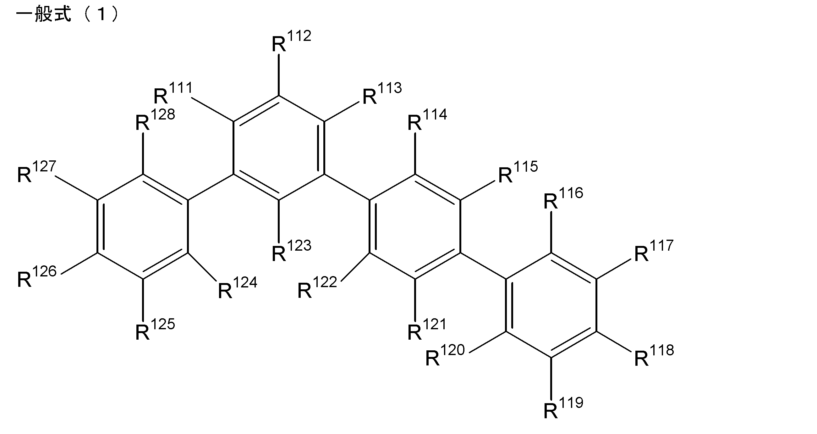
(一般式(1)中、R111~R128は水素原子または置換基を表す。R111~R122の少なくとも一つはシアノ基である。)
The charge transport material of the present invention relates to a structure represented by the general formula (1).
(In the general formula (1), R 111 to R 128 represent a hydrogen atom or a substituent. At least one of R 111 to R 122 is a cyano group.)
置換基としては、シアノ基、炭素数1~10のアルキル基、ハロゲン原子、炭素数6~30のアリール基が挙げられる。
アルキル基としては、メチル基、エチル基、イソプロピル基、n-プロピル基、t-ブチル基、s-ブチル基、n-ブチル基が好ましく、メチル基、エチル基、イソプロピル基、t-ブチル基がより好ましく、メチル基、t-ブチル基がさらに好ましく、メチル基が特に好ましい。
ハロゲン原子としては、フッ素原子が好ましい。
炭素数6~30のアリール基としては、無置換またはシアノ基で置換されたアリール基が好ましく、さらなる条件として鎖状のアリール基(1個のベンゼン環に3個以上のベンゼン環が置換されていない)であることがより好ましい。
置換基は、シアノ基、アルキル基またはアリール基が好ましく、シアノ基、アリール基がより好ましい。 Examples of the substituent include a cyano group, an alkyl group having 1 to 10 carbon atoms, a halogen atom, and an aryl group having 6 to 30 carbon atoms.
As the alkyl group, a methyl group, an ethyl group, an isopropyl group, an n-propyl group, a t-butyl group, a s-butyl group, and an n-butyl group are preferable, and a methyl group, an ethyl group, an isopropyl group, and a t-butyl group are preferable. More preferred are a methyl group and a t-butyl group, and a methyl group is particularly preferred.
As the halogen atom, a fluorine atom is preferable.
The aryl group having 6 to 30 carbon atoms is preferably an aryl group that is unsubstituted or substituted with a cyano group, and as a further condition, a chain aryl group (one benzene ring is substituted with 3 or more benzene rings). More preferred).
The substituent is preferably a cyano group, an alkyl group or an aryl group, more preferably a cyano group or an aryl group.
前記一般式(1)で表される化合物は、さらに有機電界発光素子の有機層に用いる場合において、その有機層のどの機能層に用いるかによってさらに好ましい構造が異なる。前記一般式(1)で表される化合物のさらに好ましい構造については、本発明の有機電界発光素子の説明において後述する。
In the case where the compound represented by the general formula (1) is further used in an organic layer of an organic electroluminescent element, a more preferable structure varies depending on which functional layer of the organic layer is used. A more preferable structure of the compound represented by the general formula (1) will be described later in the description of the organic electroluminescence device of the present invention.
前記一般式(1)で表される化合物の膜状態でのT1エネルギーは、56kcal/mol以上80kcal/mol以下であることが好ましく、57kcal/mol以上70kcal/mol以下であることがより好ましく、58kcal/mol以上66kcal/mol以下であることが更に好ましい。特に、発光材料として燐光発光材料を用いる場合には、T1エネルギーが上記範囲となることが好ましい。
The T 1 energy in the film state of the compound represented by the general formula (1) is preferably 56 kcal / mol or more and 80 kcal / mol or less, more preferably 57 kcal / mol or more and 70 kcal / mol or less, More preferably, it is 58 kcal / mol or more and 66 kcal / mol or less. In particular, when a phosphorescent light emitting material is used as the light emitting material, the T 1 energy is preferably in the above range.
T1エネルギーは、材料の薄膜の燐光発光スペクトルを測定し、その短波長端から求めることができる。例えば、洗浄した石英ガラス基板上に、材料を真空蒸着法により約50nmの膜厚に成膜し、薄膜の燐光発光スペクトルを液体窒素温度下でF-7000日立分光蛍光光度計(日立ハイテクノロジーズ)を用いて測定する。得られた発光スペクトルの短波長側の立ち上がり波長をエネルギー単位に換算することによりT1エネルギーを求めることができる。
The T 1 energy can be determined from the short wavelength end of a phosphorescence emission spectrum of a thin film of material. For example, a material is deposited on a cleaned quartz glass substrate to a thickness of about 50 nm by vacuum deposition, and the phosphorescence emission spectrum of the thin film is measured at F-7000 Hitachi Spectrofluorimeter (Hitachi High Technologies) under liquid nitrogen temperature. Use to measure. T 1 energy can be obtained by converting the rising wavelength on the short wavelength side of the obtained emission spectrum into energy units.
本発明の電荷輸送材料では、前記一般式(1)で表される化合物の分子量は、1000以下であることが好ましく、500~1000であることがより好ましく、600~900であることが特に好ましい。分子量をこの範囲とすることで、膜質が良好で、昇華精製・蒸着適性に優れた材料が得られる。特に、前記一般式(1)で表される化合物の分子量が600~1000であることが、蒸着適性の観点から好ましい。
In the charge transport material of the present invention, the molecular weight of the compound represented by the general formula (1) is preferably 1000 or less, more preferably 500 to 1000, and particularly preferably 600 to 900. . By setting the molecular weight within this range, a material having good film quality and excellent sublimation purification / deposition suitability can be obtained. In particular, the molecular weight of the compound represented by the general formula (1) is preferably 600 to 1000 from the viewpoint of deposition suitability.
有機電界発光素子を高温駆動時や素子駆動中の発熱に対して安定して動作させる観点から、一般式(1)で表される化合物のガラス転移温度(Tg)は80℃以上400℃以下(もしくは検出されない)であることが好ましく、100℃以上400℃以下(もしくは検出されない)であることがより好ましく、110℃以上400℃以下(もしくは検出されない)であることが更に好ましい。
The glass transition temperature (Tg) of the compound represented by the general formula (1) is 80 ° C. or higher and 400 ° C. or lower (from the viewpoint of stably operating the organic electroluminescence device against heat generated during high temperature driving or driving the device) Or not detected), more preferably 100 ° C. or higher and 400 ° C. or lower (or not detected), and even more preferably 110 ° C. or higher and 400 ° C. or lower (or not detected).
一般式(1)で表される化合物の純度が低いと、不純物が電荷輸送のトラップとして働いたり、素子の劣化を促進させたりするため、一般式(1)で表される化合物の純度は高いほど好ましい。純度は例えば高速液体クロマトグラフィー(HPLC)により測定でき、254nmの光吸収強度で検出したときの一般式(1)で表される化合物の面積比は、好ましくは99.00%以上であり、より好ましくは99.50%以上であり、特に好ましくは99.90%以上であり、最も好ましくは99.9%以上である。
When the purity of the compound represented by the general formula (1) is low, impurities work as charge transport traps or promote the deterioration of the device. Therefore, the purity of the compound represented by the general formula (1) is high. The more preferable. The purity can be measured by, for example, high performance liquid chromatography (HPLC), and the area ratio of the compound represented by the general formula (1) when detected with a light absorption intensity of 254 nm is preferably 99.00% or more, and more It is preferably 99.50% or more, particularly preferably 99.90% or more, and most preferably 99.9% or more.
国際公開第2008/117889号に記載のカルバゾール系材料で知られているように、一般式(1)で表される化合物の水素原子の一部又は全部を重水素原子で置換した材料も好ましく電荷輸送材料として用いることができる。
As known for the carbazole-based material described in WO2008 / 117889, a material in which part or all of the hydrogen atoms of the compound represented by the general formula (1) are substituted with deuterium atoms is also preferably charged. It can be used as a transport material.
一般式(1)で表される化合物の具体例を以下に示すが、本発明はこれらに限定されない。但し、前記一般式(1)で表される化合物は下記一般式(1A-1)~(1A-20)の2以上に属していてもよい。
Specific examples of the compound represented by the general formula (1) are shown below, but the present invention is not limited thereto. However, the compound represented by the general formula (1) may belong to two or more of the following general formulas (1A-1) to (1A-20).
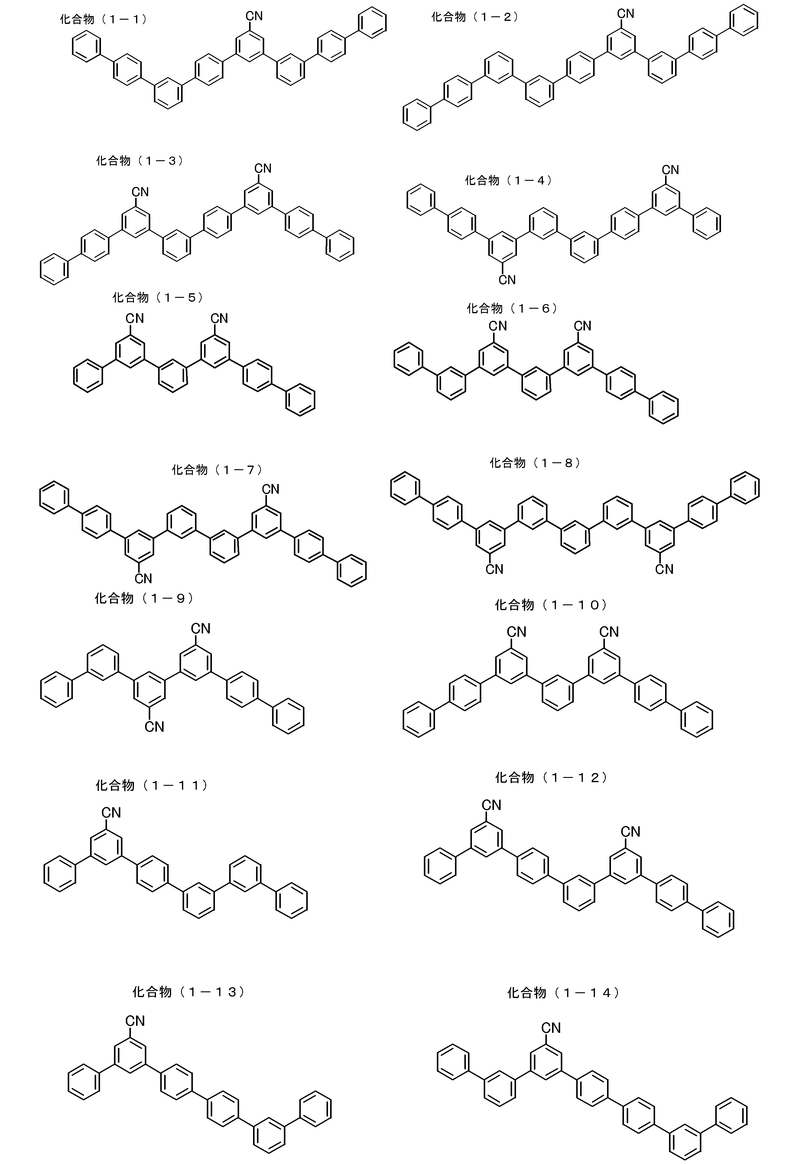

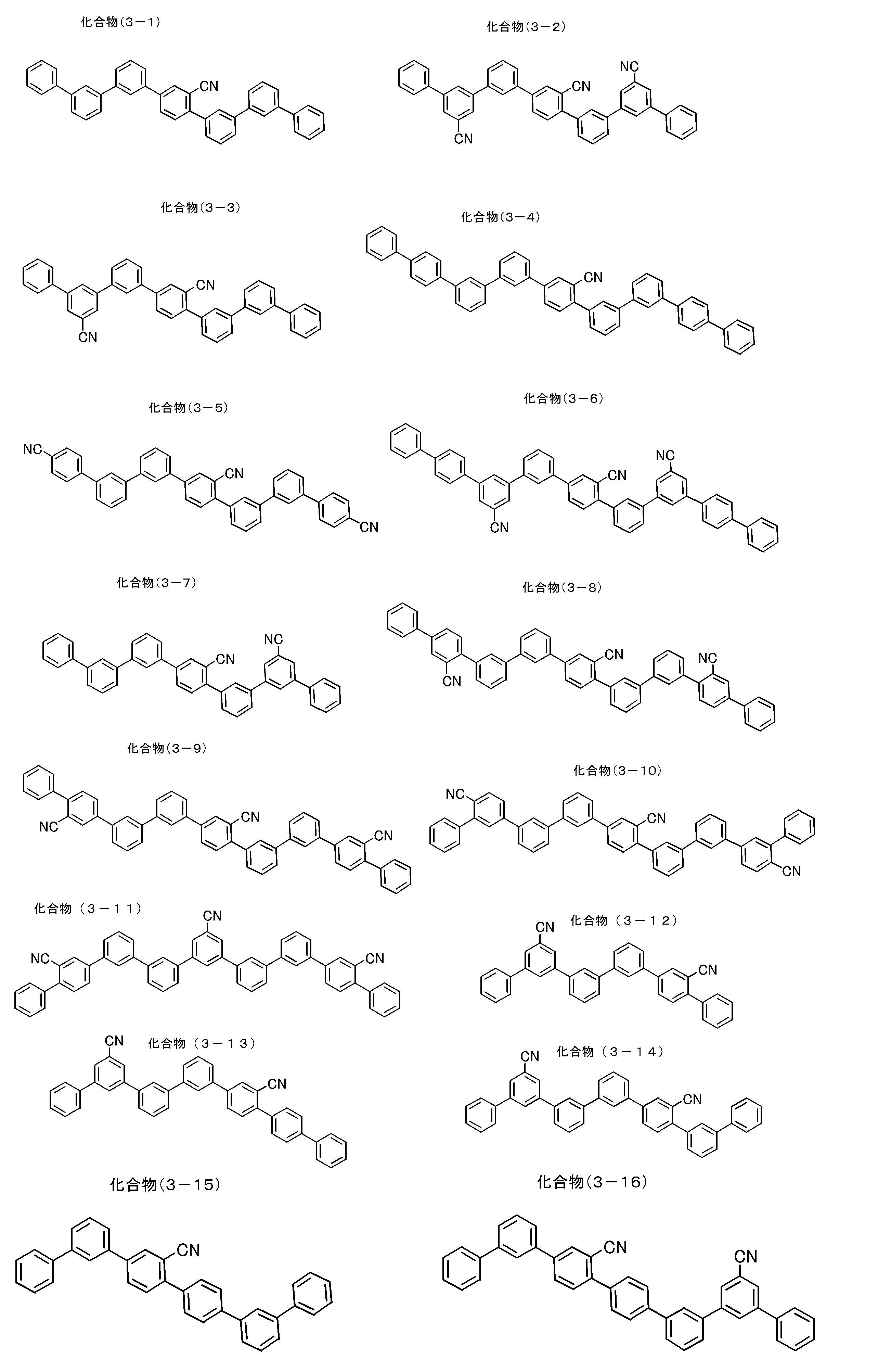
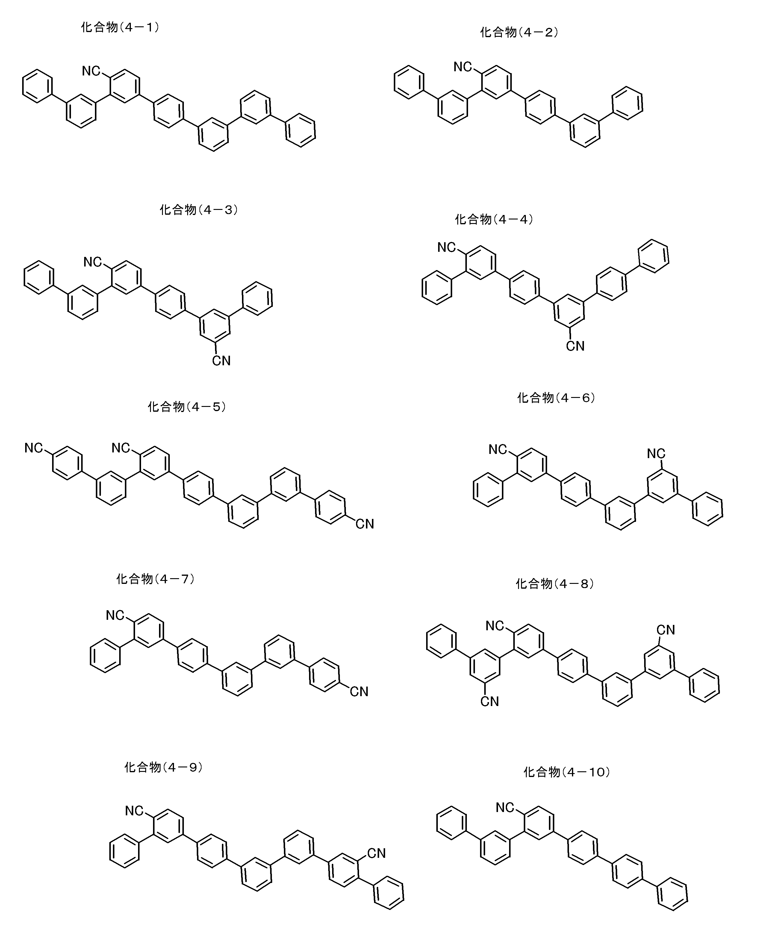
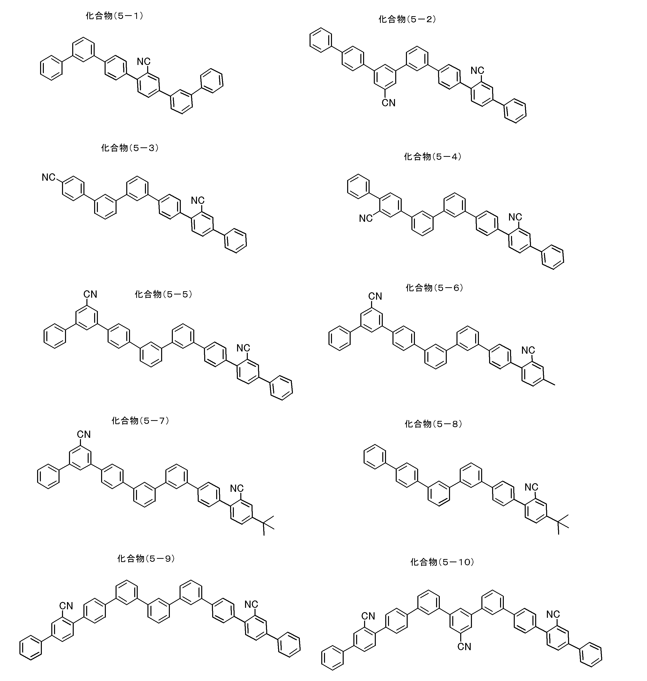
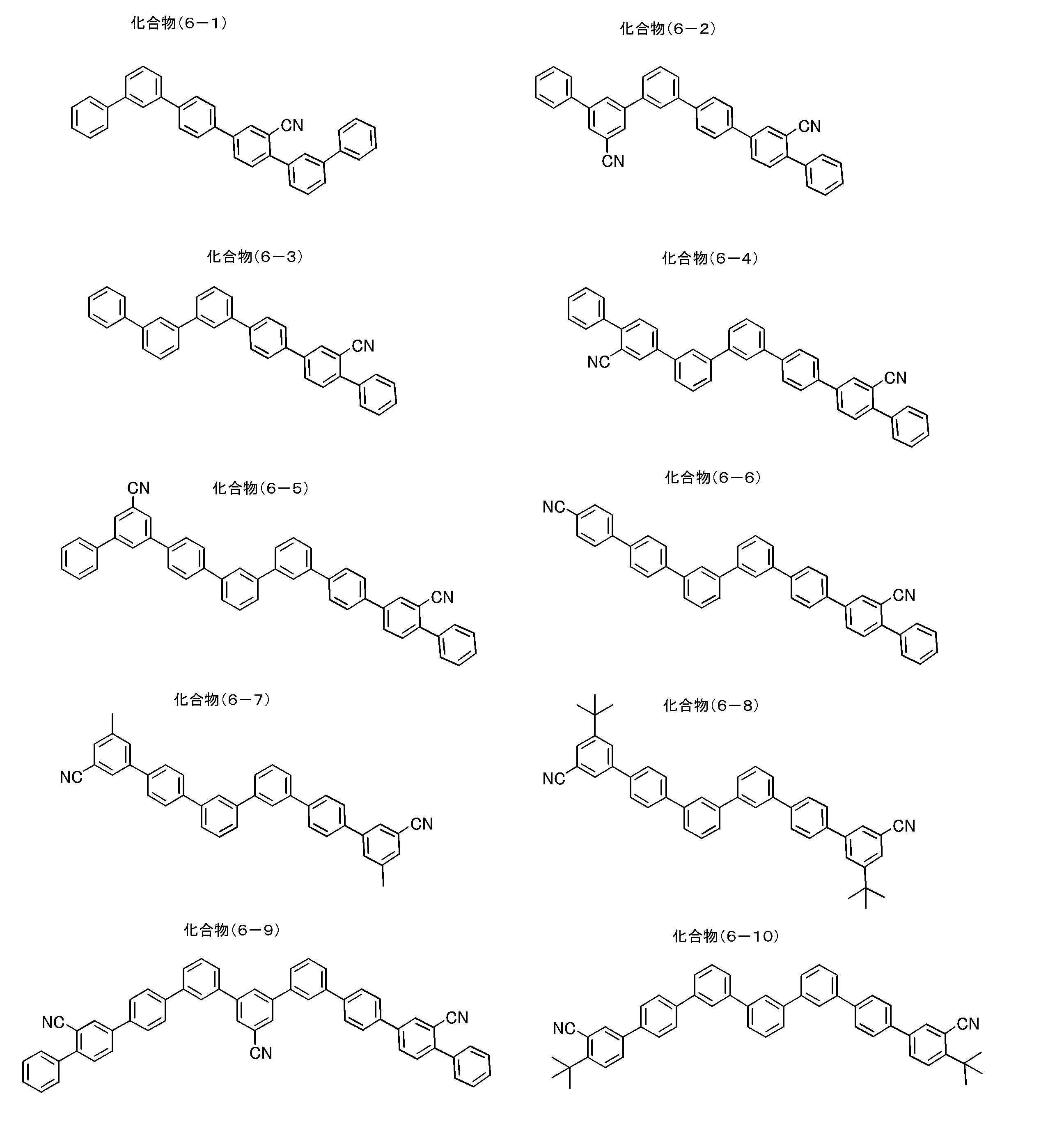
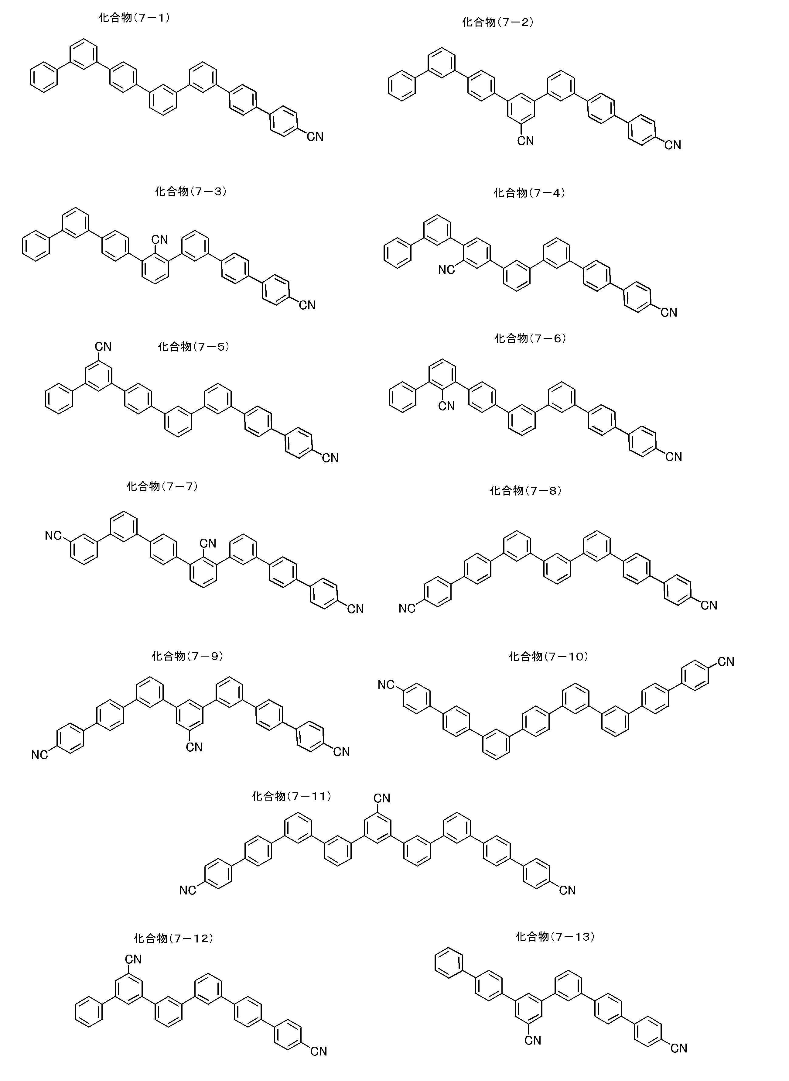
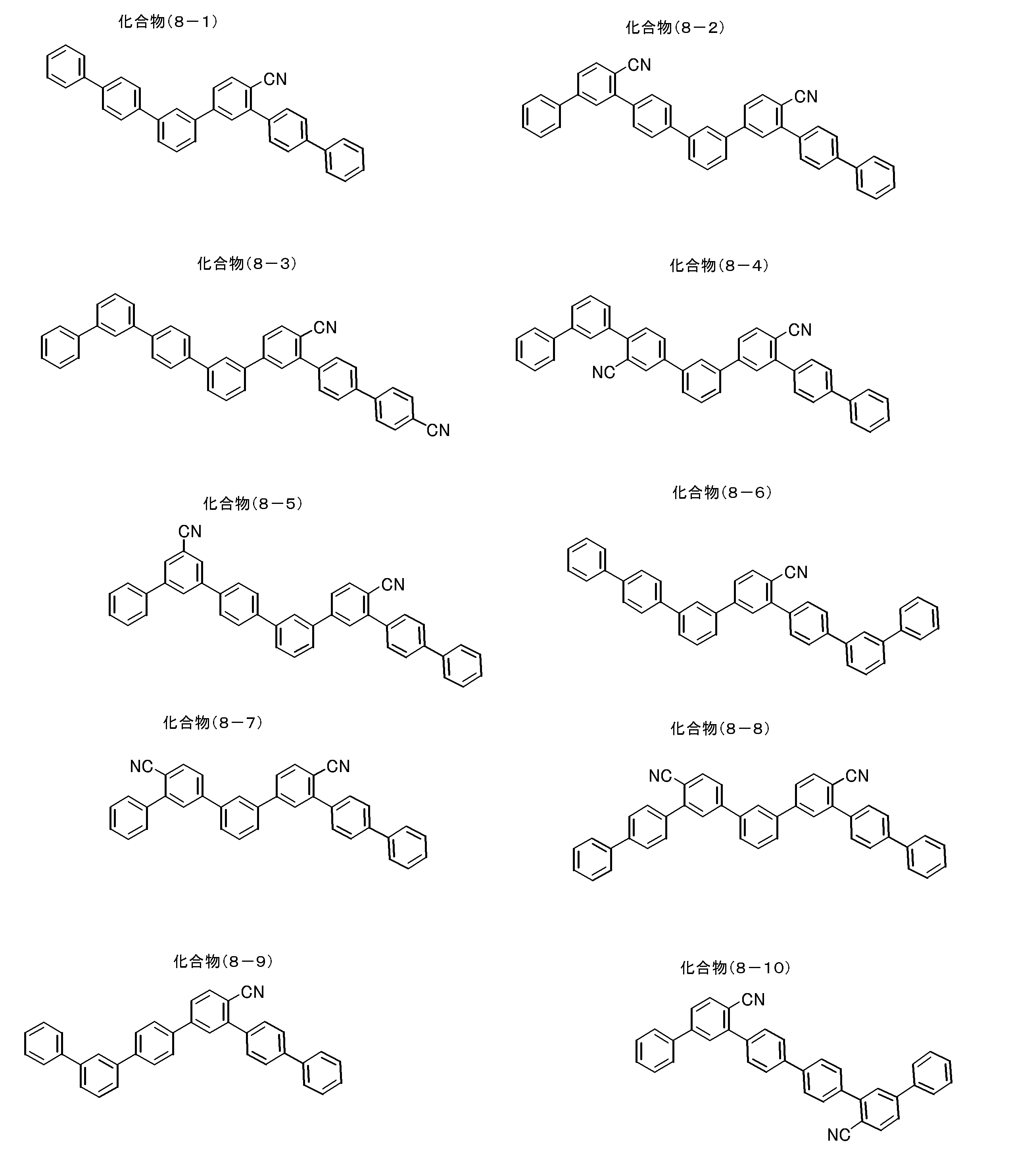

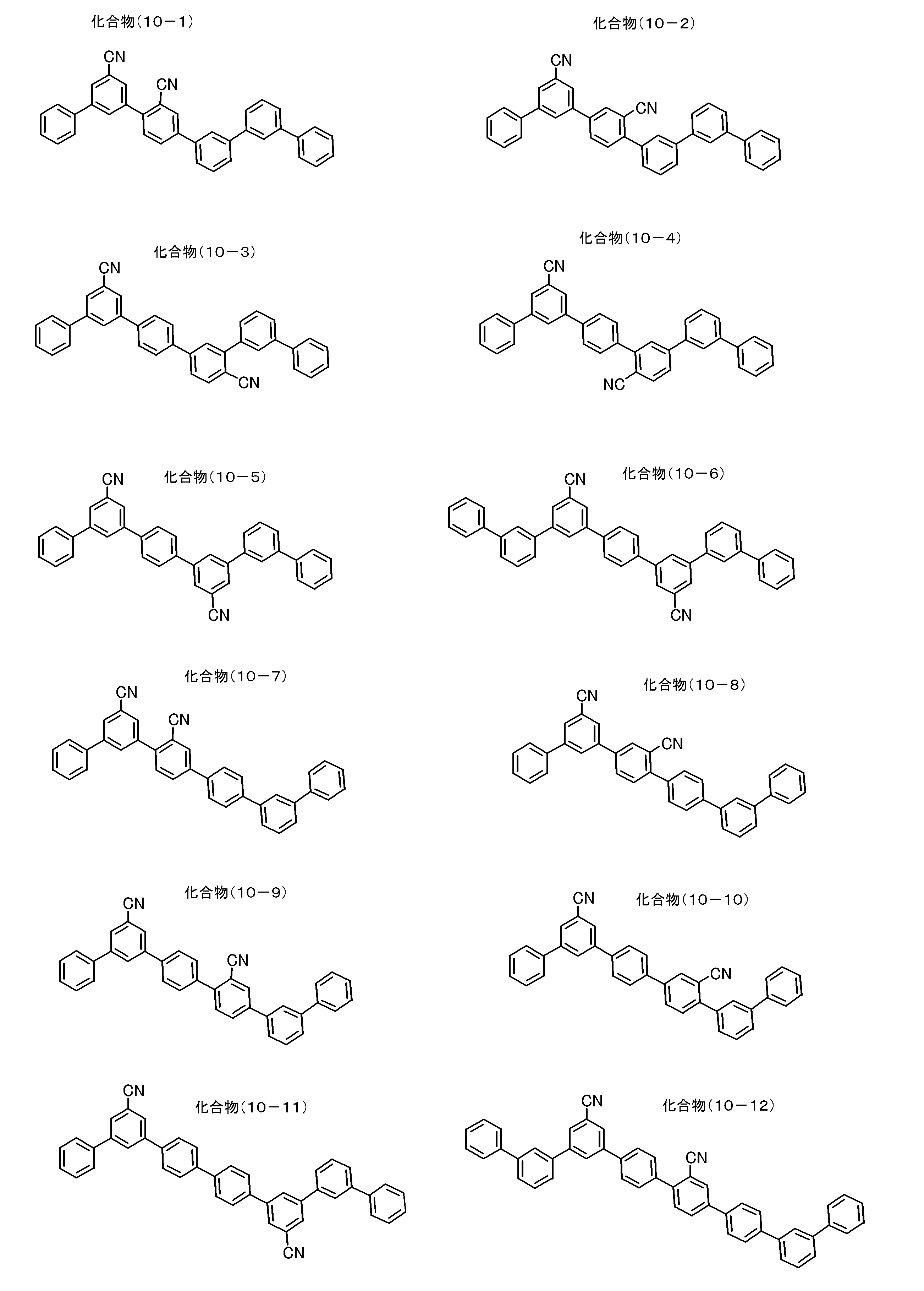
上記一般式(1)で表される化合物は、特開2007-266598等に記載の方法や、その他公知の反応を組み合わせて合成できる。
合成後、カラムクロマトグラフィー、再結晶等による精製を行った後、昇華精製により精製することが好ましい。昇華精製により、有機不純物を分離できるだけでなく、無機塩や残留溶媒等を効果的に取り除くことができる。 The compound represented by the general formula (1) can be synthesized by combining the method described in JP-A-2007-266598 and other known reactions.
After synthesis, it is preferable to purify by sublimation purification after purification by column chromatography, recrystallization or the like. By sublimation purification, not only can organic impurities be separated, but inorganic salts and residual solvents can be effectively removed.
[有機電界発光素子]
本発明の有機電界発光素子は、基板と、該基板上に配置され、陽極及び陰極を含む一対の電極と、該電極間に配置された有機層とを有し、前記有機層が、燐光発光材料と本発明の電荷輸送材料、すなわち前記一般式(1)で表される化合物を含むことを特徴とする。
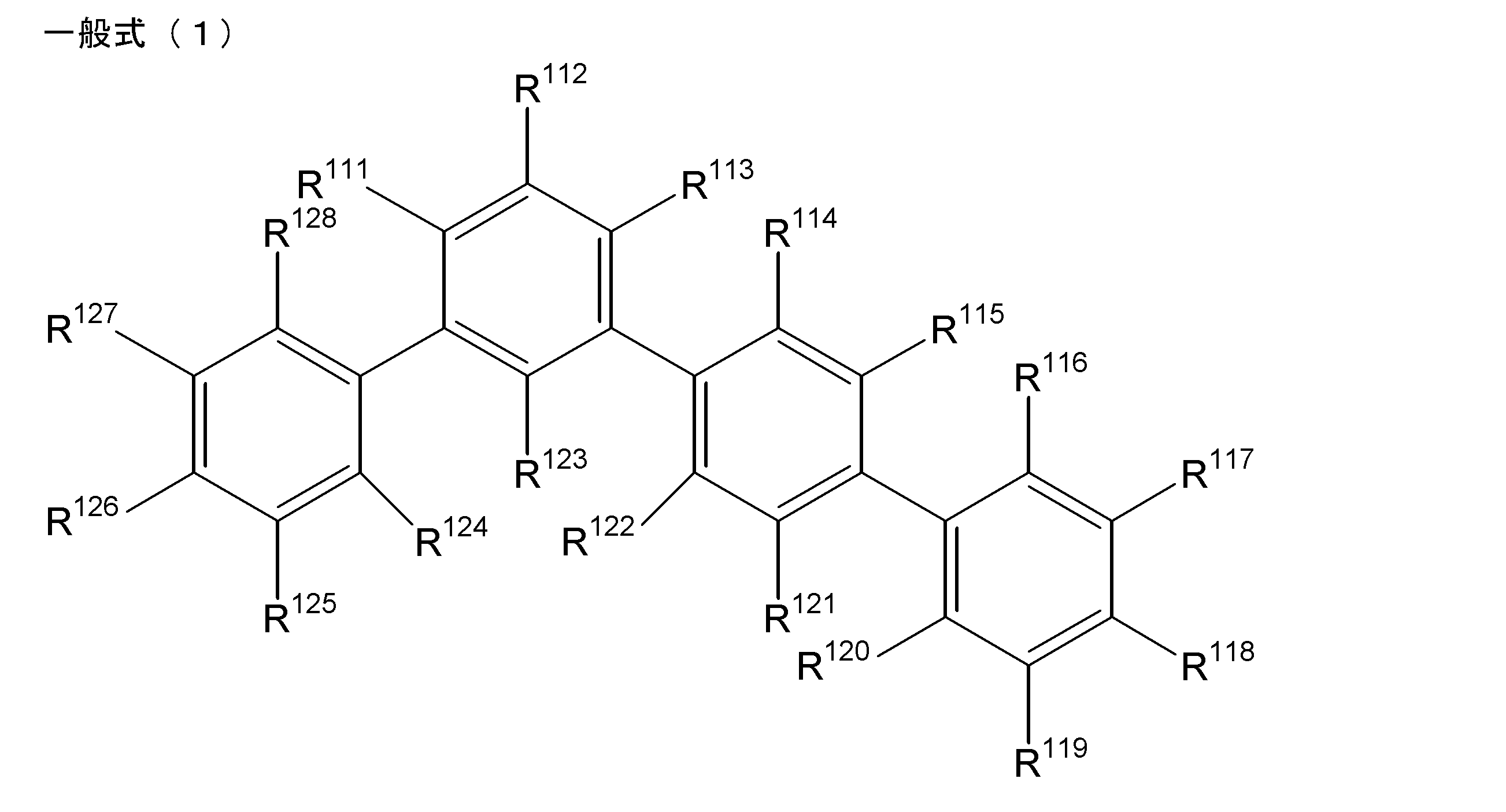
(一般式(1)中、R111~R128は水素原子または置換基を表す。R111~R122の少なくとも1個はシアノ基である。但し、連続する3個のベンゼン環のそれぞれにシアノ基を有することはなく、シアノ基を有するベンゼン環が3個以上のベンゼン環で置換されることはない。)
[Organic electroluminescence device]
The organic electroluminescent element of the present invention has a substrate, a pair of electrodes including an anode and a cathode disposed on the substrate, and an organic layer disposed between the electrodes, and the organic layer emits phosphorescence. It contains the material and the charge transport material of the present invention, that is, the compound represented by the general formula (1).
(In the general formula (1), R 111 to R 128 each represent a hydrogen atom or a substituent. At least one of R 111 to R 122 is a cyano group, provided that each of the three consecutive benzene rings has a cyano group. The benzene ring having a cyano group is not substituted with three or more benzene rings.
本発明の有機電界発光素子は、基板と、該基板上に配置され、陽極及び陰極を含む一対の電極と、該電極間に配置された有機層とを有し、前記有機層が、燐光発光材料と本発明の電荷輸送材料、すなわち前記一般式(1)で表される化合物を含むことを特徴とする。
The organic electroluminescent element of the present invention has a substrate, a pair of electrodes including an anode and a cathode disposed on the substrate, and an organic layer disposed between the electrodes, and the organic layer emits phosphorescence. It contains the material and the charge transport material of the present invention, that is, the compound represented by the general formula (1).
本発明の有機電界発光素子の構成は、特に制限されることはない。図1に、本発明の有機電界発光素子の構成の一例を示す。図1の有機電界発光素子10は、基板2上に、一対の電極(陽極3と陰極9)の間に有機層を有する。
有機電界発光素子の素子構成、基板、陰極及び陽極については、例えば、特開2008-270736号公報に詳述されており、該公報に記載の事項を本発明に適用することができる。
以下、本発明の有機電界発光素子の好ましい態様について、基板、電極、有機層、保護層、封止容器、駆動方法、発光ピーク波長、用途の順で詳細に説明する。 The structure of the organic electroluminescent element of the present invention is not particularly limited. In FIG. 1, an example of a structure of the organic electroluminescent element of this invention is shown. 1 has an organic layer on asubstrate 2 between a pair of electrodes (anode 3 and cathode 9).
The element configuration, the substrate, the cathode, and the anode of the organic electroluminescence element are described in detail in, for example, Japanese Patent Application Laid-Open No. 2008-270736, and the matters described in the publication can be applied to the present invention.
Hereinafter, the preferable aspect of the organic electroluminescent element of this invention is demonstrated in detail in order of a board | substrate, an electrode, an organic layer, a protective layer, a sealing container, a drive method, an emission peak wavelength, and a use.
有機電界発光素子の素子構成、基板、陰極及び陽極については、例えば、特開2008-270736号公報に詳述されており、該公報に記載の事項を本発明に適用することができる。
以下、本発明の有機電界発光素子の好ましい態様について、基板、電極、有機層、保護層、封止容器、駆動方法、発光ピーク波長、用途の順で詳細に説明する。 The structure of the organic electroluminescent element of the present invention is not particularly limited. In FIG. 1, an example of a structure of the organic electroluminescent element of this invention is shown. 1 has an organic layer on a
The element configuration, the substrate, the cathode, and the anode of the organic electroluminescence element are described in detail in, for example, Japanese Patent Application Laid-Open No. 2008-270736, and the matters described in the publication can be applied to the present invention.
Hereinafter, the preferable aspect of the organic electroluminescent element of this invention is demonstrated in detail in order of a board | substrate, an electrode, an organic layer, a protective layer, a sealing container, a drive method, an emission peak wavelength, and a use.
<基板>
本発明の有機電界発光素子は、基板を有する。
本発明で使用する基板としては、有機層から発せられる光を散乱又は減衰させない基板であることが好ましい。有機材料の場合には、耐熱性、寸法安定性、耐溶剤性、電気絶縁性、及び加工性に優れていることが好ましい。 <Board>
The organic electroluminescent element of the present invention has a substrate.
The substrate used in the present invention is preferably a substrate that does not scatter or attenuate light emitted from the organic layer. In the case of an organic material, it is preferable that it is excellent in heat resistance, dimensional stability, solvent resistance, electrical insulation, and workability.
<電極>
本発明の有機電界発光素子は、前記基板上に配置され、陽極及び陰極を含む一対の電極を有する。
発光素子の性質上、一対の電極である陽極及び陰極のうち少なくとも一方の電極は、透明若しくは半透明であることが好ましい。 <Electrode>
The organic electroluminescent element of the present invention is disposed on the substrate and has a pair of electrodes including an anode and a cathode.
In view of the properties of the light-emitting element, at least one of the pair of electrodes, the anode and the cathode, is preferably transparent or translucent.
(陽極)
陽極は、通常、有機層に正孔を供給する電極としての機能を有していればよく、その形状、構造、大きさ等については特に制限はなく、発光素子の用途、目的に応じて、公知の電極材料の中から適宜選択することができる。前述のごとく、陽極は、通常透明陽極として設けられる。 (anode)
The anode usually only needs to have a function as an electrode for supplying holes to the organic layer, and there is no particular limitation on the shape, structure, size, etc., depending on the use and purpose of the light-emitting element, It can select suitably from well-known electrode materials. As described above, the anode is usually provided as a transparent anode.
(陰極)
陰極は、通常、有機層に電子を注入する電極としての機能を有していればよく、その形状、構造、大きさ等については特に制限はなく、発光素子の用途、目的に応じて、公知の電極材料の中から適宜選択することができる。 (cathode)
The cathode usually has a function as an electrode for injecting electrons into the organic layer, and there is no particular limitation on the shape, structure, size, etc., and it is known depending on the use and purpose of the light-emitting element. The electrode material can be selected as appropriate.
<有機層>
本発明の有機電界発光素子は、前記電極間に配置された有機層を有し、前記有機層が、燐光発光材料と前記一般式(1)で表される化合物を含むことを特徴とする。
前記有機層は、特に制限はなく、有機電界発光素子の用途、目的に応じて適宜選択することができるが、前記透明電極上に又は前記半透明電極上に形成されるのが好ましい。この場合、有機層は、前記透明電極又は前記半透明電極上の全面又は一面に形成される。
有機層の形状、大きさ、及び厚み等については、特に制限はなく、目的に応じて適宜選択することができる。
以下、本発明の有機電界発光素子における、有機層の構成、有機層の形成方法、有機層を構成する各層の好ましい態様および各層に使用される材料について順に説明する。 <Organic layer>
The organic electroluminescent element of the present invention has an organic layer disposed between the electrodes, and the organic layer includes a phosphorescent material and a compound represented by the general formula (1).
There is no restriction | limiting in particular in the said organic layer, Although it can select suitably according to the use and objective of an organic electroluminescent element, It is preferable to form on the said transparent electrode or the said semi-transparent electrode. In this case, the organic layer is formed on the entire surface or one surface of the transparent electrode or the semitransparent electrode.
There is no restriction | limiting in particular about the shape of a organic layer, a magnitude | size, thickness, etc., According to the objective, it can select suitably.
Hereinafter, in the organic electroluminescent element of the present invention, the configuration of the organic layer, the method for forming the organic layer, preferred embodiments of the layers constituting the organic layer, and materials used for the layers will be described in order.
(有機層の構成)
本発明の有機電界発光素子では、前記有機層が、電荷輸送層を含むことが好ましい。
電荷輸送層とは、有機電界発光素子に電圧を印加した際に電荷移動が起こる層をいう。
具体的には正孔注入層、正孔輸送層、電子ブロック層、発光層、正孔ブロック層、電子輸送層又は電子注入層が挙げられる。好ましくは、正孔注入層、正孔輸送層、電子ブロック層又は発光層である。塗布法により形成される電荷輸送層が正孔注入層、正孔輸送層、電子ブロック層又は発光層であれば、低コストかつ高効率な有機電界発光素子の製造が可能となる。また、電荷輸送層として、より好ましくは、正孔注入層、正孔輸送層又は電子ブロック層である。
本発明の有機電界発光素子では、前記燐光発光材料を含む発光層とその他の有機層を有し、前記発光層が前記一般式(1)で表される化合物を含有することが好ましい。さらに、本発明の有機電界発光素子では、前記有機層が、前記燐光発光材料を含む発光層とその他の有機層を有すことがより好ましい。但し、本発明の有機電界発光素子は、前記有機層が発光層とその他の有機層を有する場合であっても、必ずしも明確に層間が区別されなくてもよい。 (Organic layer structure)
In the organic electroluminescent element of the present invention, the organic layer preferably includes a charge transport layer.
The charge transport layer is a layer in which charge transfer occurs when a voltage is applied to the organic electroluminescent element.
Specific examples include a hole injection layer, a hole transport layer, an electron block layer, a light emitting layer, a hole block layer, an electron transport layer, and an electron injection layer. A hole injection layer, a hole transport layer, an electron blocking layer, or a light emitting layer is preferable. If the charge transport layer formed by the coating method is a hole injection layer, a hole transport layer, an electron blocking layer, or a light emitting layer, it is possible to manufacture an organic electroluminescent element with low cost and high efficiency. The charge transport layer is more preferably a hole injection layer, a hole transport layer, or an electron block layer.
The organic electroluminescent element of the present invention preferably has a light emitting layer containing the phosphorescent material and another organic layer, and the light emitting layer contains the compound represented by the general formula (1). Furthermore, in the organic electroluminescent element of the present invention, it is more preferable that the organic layer has a light emitting layer containing the phosphorescent material and another organic layer. However, in the organic electroluminescent element of the present invention, even when the organic layer has a light emitting layer and other organic layers, the layers do not necessarily have to be clearly distinguished.
本発明の有機電界発光素子は、前記有機層が燐光発光材料と前記一般式(1)で表される化合物を含む。このとき、前記燐光発光材料と前記一般式(1)で表される化合物が含まれる場所に特に制限はない。本発明では、前記有機層が、前記燐光発光材料を含む発光層とその他の有機層を有し、前記発光層が前記一般式(1)で表される化合物を含有することがより好ましい。このとき、前記一般式(1)で表される化合物が、発光層のホスト材料(以下、ホスト化合物とも言う)として用いられることが好ましい。
In the organic electroluminescent element of the present invention, the organic layer contains a phosphorescent material and a compound represented by the general formula (1). At this time, there is no particular limitation on the place where the phosphorescent material and the compound represented by the general formula (1) are included. In this invention, it is more preferable that the said organic layer has the light emitting layer containing the said phosphorescence-emitting material, and another organic layer, and the said light emitting layer contains the compound represented by the said General formula (1). At this time, it is preferable that the compound represented by the general formula (1) is used as a host material of the light emitting layer (hereinafter also referred to as a host compound).
本発明において、一般式(1)で表される化合物は、その用途が限定されることはなく、有機電界発光素子の陰極と陽極の間の有機層内のいずれの層に含有されてもよい。一般式(1)で表される化合物の導入層としては、発光層、発光層と陰極との間の層、発光層と陽極との間の層のいずれかまたは複数に含有されるのが好ましく、発光層、正孔注入層、正孔輸送層、電子輸送層、電子注入層、励起子ブロック層、電荷ブロック層(正孔ブロック層、電子ブロック層など)のいずれか、または複数に含有されるのがより好ましく、発光層、励起子ブロック層、電荷ブロック層、電子輸送層、電子注入層のいずれかに含有されることが特に好ましく、発光層または正孔ブロック層のいずれかに含有されることがより特に好ましい。
本発明では、一般式(1)で表される化合物を発光層、発光層と陰極との間で発光層に隣接する有機層(発光層に隣接する陰極側の層)、及び発光層側で陰極に隣接する電子注入層のいずれかに含有されることが好ましく、発光層及び発光層に隣接する陰極側の層のいずれかに含有されることがより好ましく、発光層に含有されることが更に好ましい。また、一般式(1)で表される化合物を発光層及び発光層に隣接する陰極側の層の両層に含有させてもよい。 In the present invention, the compound represented by the general formula (1) is not limited in its application, and may be contained in any layer in the organic layer between the cathode and the anode of the organic electroluminescence device. . The introduction layer of the compound represented by the general formula (1) is preferably contained in one or more of the light emitting layer, the layer between the light emitting layer and the cathode, and the layer between the light emitting layer and the anode. , Light-emitting layer, hole injection layer, hole transport layer, electron transport layer, electron injection layer, exciton block layer, charge block layer (hole block layer, electron block layer, etc.) More preferably, it is contained in any one of the light emitting layer, exciton blocking layer, charge blocking layer, electron transporting layer, and electron injection layer, and contained in either the light emitting layer or the hole blocking layer. More particularly preferred.
In the present invention, the compound represented by the general formula (1) is added to the light emitting layer, the organic layer adjacent to the light emitting layer between the light emitting layer and the cathode (the cathode side layer adjacent to the light emitting layer), and the light emitting layer side. It is preferably contained in any of the electron injection layers adjacent to the cathode, more preferably contained in any of the light emitting layer and the cathode side layer adjacent to the light emitting layer, and contained in the light emitting layer. Further preferred. Further, the compound represented by the general formula (1) may be contained in both the light emitting layer and the cathode side layer adjacent to the light emitting layer.
《一般式(1)で表される化合物を発光層中に発光層のホスト材料として含有させる場合》
一般式(1)で表される化合物を発光層中に発光層のホスト材料として含有させる場合、一般式(1)で表される化合物は発光層の全質量に対して0.1~99質量%含ませることが好ましく、1~97質量%含ませることがより好ましく、10~96質量%含ませることが更に好ましい。 << When the compound represented by the general formula (1) is contained in the light emitting layer as a host material of the light emitting layer >>
When the compound represented by the general formula (1) is contained in the light emitting layer as a host material of the light emitting layer, the compound represented by the general formula (1) is 0.1 to 99 mass with respect to the total mass of the light emitting layer. %, Preferably 1 to 97% by mass, more preferably 10 to 96% by mass.
一般式(1)で表される化合物を発光層のホスト材料として用いる場合、低電圧化および発光効率の観点から、LUMOレベルが-1.90eV以上-1.20eV未満の範囲となることが好ましく、-1.80eV以上-1.30eV未満の範囲となることがより好ましく、-1.70eV以上-1.40eV未満の範囲となることが更に好ましい。この理由は、電子輸送層から発光層への電子注入性を向上させ駆動電圧を低下させるためである。
なお、本明細書中に記載した一般式(1)で表される化合物の具体的なLUMOレベル(最低空軌道エネルギー)は、B3LYP/6-31G(d)//B3LYP/6-31G(d)レベルでの量子化学計算を行い求めた値である。
同じ電子求引基であっても置換位置の違いにより、LUMOレベルを大きくする程度が異なる。傾向としては、前記一般式(2)におけるR111、R118が最も影響が大きく、次にR114、R115、R121、R122、その次にR113、R116およびR120、その次にR117およびR119その次にR112、最も影響が小さいのはR123およびR124~R128であるが、必ずしもこのような順になるとは限らない。
この場合、前記発光層が発光層のホスト材料として、前記一般式(1)で表される構造の化合物として、下記一般式(1A)で表される部分構造を含むことが、前述のLUMOレベル-1.90eV以上-1.20eV未満の範囲を実現する観点からより好ましい。 When the compound represented by the general formula (1) is used as the host material of the light emitting layer, the LUMO level is preferably in the range of −1.90 eV or more and less than −1.20 eV from the viewpoint of lowering the voltage and light emission efficiency. More preferably, the range is from −1.80 eV to less than −1.30 eV, and even more preferably from −1.70 eV to less than −1.40 eV. This is because the electron injection property from the electron transport layer to the light emitting layer is improved and the driving voltage is lowered.
The specific LUMO level (lowest orbital energy) of the compound represented by the general formula (1) described in this specification is B3LYP / 6-31G (d) // B3LYP / 6-31G (d ) Is the value obtained by performing quantum chemical calculations at the level.
Even with the same electron-withdrawing group, the degree of increasing the LUMO level varies depending on the substitution position. As the tendency, R 111 and R 118 in the general formula (2) have the largest influence, followed by R 114 , R 115 , R 121 , R 122 , then R 113 , R 116 and R 120 , and then R 117 and R 119 and then R 112 , and R 123 and R 124 to R 128 have the least influence, but they are not always in this order.
In this case, the LUMO level described above includes that the light emitting layer includes a partial structure represented by the following general formula (1A) as a compound having the structure represented by the general formula (1) as a host material of the light emitting layer. It is more preferable from the viewpoint of realizing a range of -1.90 eV or more and less than -1.20 eV.
まず、前記一般式(1)で表される構造の化合物が一般式(1A)で表される部分構造である態様について説明する。
First, an embodiment in which the compound having the structure represented by the general formula (1) is a partial structure represented by the general formula (1A) will be described.
一方、前記一般式(1)で表される部分構造の中でも、より好ましい部分構造である下記一般式(1A-1)~(1A-20)で表される部分構造を以下に示すが、本発明は以下の具体例に限定されるものではない。なお、下記具体例の代表的な部分構造のLUMOレベルとしては、下記一般式(1A-1)で表される部分構造は-1.51eVであり、下記一般式(1A-2)、一般式(1A-3)で表される部分構造は-1.58eVであり、下記一般式(1A-5)で表される部分構造は-1.56eVであり、下記一般式(1A-6)で表される部分構造は-1.54eVであり、下記一般式(1A-7)で表される部分構造は-1.76eVである。
下記一般式(1A-11)で表される部分構造は-1.87eVであり、下記一般式(1A-12)で表される部分構造は-1.85eVであり、下記一般式(1A-13)で表される部分構造は-1.73eVであり、下記一般式(1A-14)で表される部分構造は-1.75eVであり、下記一般式(1A-17)で表される部分構造は-1.91eVであり、下記一般式(1A-18)で表される部分構造は-1.79eVであり、下記一般式(1A-19)で表される部分構造は-1.82eVであり、下記一般式(1A-20)で表される部分構造は-2.01eVである。 On the other hand, among the partial structures represented by the general formula (1), partial structures represented by the following general formulas (1A-1) to (1A-20), which are more preferable partial structures, are shown below. The invention is not limited to the following specific examples. As the LUMO level of the representative partial structure of the specific examples below, the partial structure represented by the following general formula (1A-1) is −1.51 eV, and the following general formula (1A-2), The partial structure represented by (1A-3) is -1.58 eV, the partial structure represented by the following general formula (1A-5) is -1.56 eV, and the following general formula (1A-6) The partial structure represented is −1.54 eV, and the partial structure represented by the following general formula (1A-7) is −1.76 eV.
The partial structure represented by the following general formula (1A-11) is −1.87 eV, the partial structure represented by the following general formula (1A-12) is −1.85 eV, and the following general formula (1A- The partial structure represented by 13) is -1.73 eV, the partial structure represented by the following general formula (1A-14) is -1.75 eV, and is represented by the following general formula (1A-17) The partial structure is -1.91 eV, the partial structure represented by the following general formula (1A-18) is -1.79 eV, and the partial structure represented by the following general formula (1A-19) is -1. The partial structure represented by the following general formula (1A-20) is -2.01 eV.
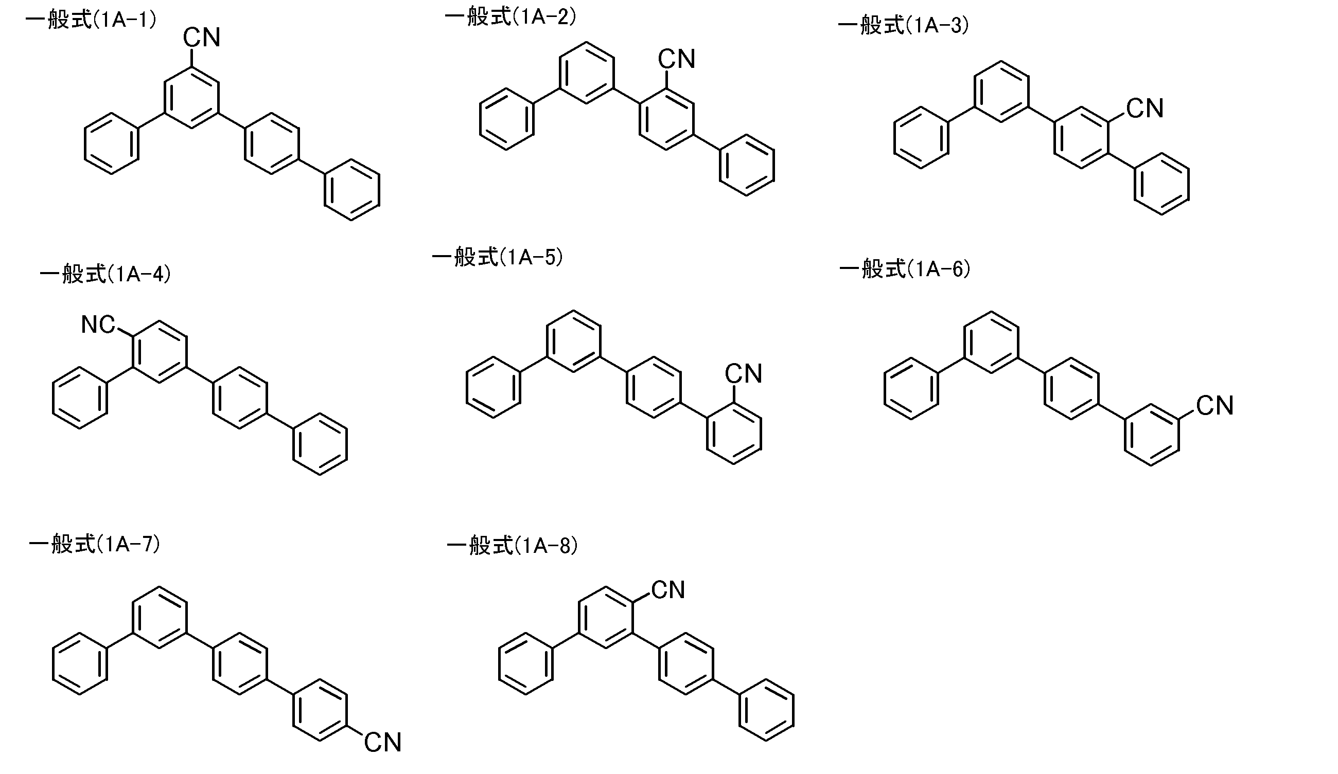
前記一般式(1)で表される化合物を発光層のホスト材料として用いる場合、発光材料の極大発光波長(以下、発光ピーク波長とも言う)は、400~700nmであることが好ましく、470~650nmであることがより好ましく、490~620nmであることがさらに好ましく、500~610nmであることが最も好ましい。
When the compound represented by the general formula (1) is used as the host material of the light emitting layer, the maximum light emission wavelength (hereinafter also referred to as emission peak wavelength) of the light emitting material is preferably 400 to 700 nm, and 470 to 650 nm. Is more preferably 490 to 620 nm, and most preferably 500 to 610 nm.
《一般式(1)で表される化合物を発光層以外の層に含有させる場合》
前記有機層が、前記燐光発光材料を含む発光層とその他の有機層を有し、前記発光層と前記陰極との間に配置されたその他の有機層が、前記一般式(1)で表される構造の化合物を含有することも好ましい。その中でも、前記有機層が電子輸送層または正孔ブロック層(より好ましくは正孔ブロック層)を有し、前記電子輸送層または前記正孔ブロック層が前記一般式(1)で表される化合物を含有することがより好ましい。前記一般式(1)で表される化合物を発光層以外の層に含有させる場合は、該発光層以外の層の全質量に対して70~100質量%含まれることが好ましく、80~100質量%含まれることがより好ましい。 << When the compound represented by General formula (1) is contained in layers other than a light emitting layer >>
The organic layer includes a light emitting layer containing the phosphorescent material and another organic layer, and the other organic layer disposed between the light emitting layer and the cathode is represented by the general formula (1). It is also preferable to contain a compound having a structure. Among them, the organic layer has an electron transport layer or a hole blocking layer (more preferably, a hole blocking layer), and the electron transport layer or the hole blocking layer is represented by the general formula (1). It is more preferable to contain. When the compound represented by the general formula (1) is contained in a layer other than the light emitting layer, it is preferably contained in an amount of 70 to 100% by mass, based on the total mass of the layer other than the light emitting layer, and 80 to 100% by mass. % Is more preferable.
本発明の化合物を電子輸送層に用いる場合、低電圧化の観点から、LUMOレベルが-2.10eV以上-1.50eV未満の範囲となることが好ましく、-2.00eV以上-1.55eV未満の範囲となることがより好ましく、-1.90eV以上-1.60eV未満の範囲となることが更に好ましい。この理由は、陰極から電子輸送層への電子注入性を向上させ、かつ、発光層への電子注入性を向上させるためである。
この場合、前記発光層と前記陰極との間に配置されたその他の有機層が前記一般式(1)で表される構造の化合物として、前記一般式(1A)で表される部分構造を含むことが前述のLUMOレベル-2.10eV以上-1.50eV未満の範囲を実現する観点から好ましい。 When the compound of the present invention is used in the electron transport layer, from the viewpoint of lowering the voltage, the LUMO level is preferably in the range of −2.10 eV or more and less than −1.50 eV, preferably −2.00 eV or more and less than −1.55 eV. Is more preferable, and a range of −1.90 eV or more and less than −1.60 eV is even more preferable. This is because the electron injecting property from the cathode to the electron transporting layer is improved and the electron injecting property to the light emitting layer is improved.
In this case, the other organic layer disposed between the light emitting layer and the cathode includes a partial structure represented by the general formula (1A) as a compound having a structure represented by the general formula (1). Is preferable from the viewpoint of realizing the above-mentioned LUMO level of −2.10 eV or more and less than −1.50 eV.
前記一般式(4-A)で表される部分構造の中でも、本発明では、前記発光層と前記陰極との間に配置されたその他の有機層が、前記一般式(1)で表される構造の化合物として、下記部分構造群A'で表される部分構造を有する化合物を含有することがより好ましいが、本発明は以下の具体例に限定されるものではない。
Among the partial structures represented by the general formula (4-A), in the present invention, another organic layer disposed between the light emitting layer and the cathode is represented by the general formula (1). Although it is more preferable to contain a compound having a partial structure represented by the following partial structure group A ′ as a structural compound, the present invention is not limited to the following specific examples.
一方、本発明では、前記発光層と前記陰極との間に配置されたその他の有機層が、前記一般式(1)で表される構造の化合物として、前記部分構造群(1A)で表される部分構造を有する化合物を含有することも好ましい。
On the other hand, in this invention, the other organic layer arrange | positioned between the said light emitting layer and the said cathode is represented by the said partial structure group (1A) as a compound of the structure represented by the said General formula (1). It is also preferable to contain a compound having a partial structure.
これらの有機層は、それぞれ複数層設けてもよく、複数層設ける場合には同一の材料で形成してもよいし、層毎に異なる材料で形成してもよい。
These organic layers may be provided in a plurality of layers, and when a plurality of layers are provided, they may be formed of the same material or different materials for each layer.
(有機層の形成方法)
本発明の有機電界発光素子において、各有機層は、蒸着法やスパッタ法等の乾式製膜法、転写法、印刷法、スピンコート法、バーコート法等の湿式製膜法(溶液塗布法)のいずれによっても好適に形成することができる。
本発明の有機電界発光素子は、前記一対の電極間に配置された有機層が、少なくとも一層の前記一般式(1)で表される化合物を含む組成物の蒸着により形成された層を含むことが好ましい。 (Formation method of organic layer)
In the organic electroluminescence device of the present invention, each organic layer is formed by a dry film forming method such as a vapor deposition method or a sputtering method, a wet film forming method such as a transfer method, a printing method, a spin coating method, or a bar coating method (solution coating method). Any of these can be suitably formed.
In the organic electroluminescent element of the present invention, the organic layer disposed between the pair of electrodes includes at least one layer formed by vapor deposition of a composition containing the compound represented by the general formula (1). Is preferred.
(発光層)
発光層は、電界印加時に、陽極、正孔注入層又は正孔輸送層から正孔を受け取り、陰極、電子注入層又は電子輸送層から電子を受け取り、正孔と電子の再結合の場を提供して発光させる機能を有する層である。但し、本発明における前記発光層は、このようなメカニズムによる発光に必ずしも限定されるものではない。本発明の有機電界発光素子における発光層は、少なくとも一種の燐光発光材料を含有することが好ましい。 (Light emitting layer)
The light emitting layer receives holes from the anode, hole injection layer or hole transport layer and receives electrons from the cathode, electron injection layer or electron transport layer when an electric field is applied, and provides a field for recombination of holes and electrons. And a layer having a function of emitting light. However, the light emitting layer in the present invention is not necessarily limited to light emission by such a mechanism. The light emitting layer in the organic electroluminescent element of the present invention preferably contains at least one phosphorescent material.
本発明の有機電界発光素子における前記発光層は、前記発光材料のみで構成されていてもよく、ホスト材料と前記発光材料の混合層とした構成でもよい。前記発光材料の種類は一種であっても二種以上であってもよい。前記ホスト材料は電荷輸送材料であることが好ましい。前記ホスト材料は一種であっても二種以上であってもよく、例えば、電子輸送性のホスト材料とホール輸送性のホスト材料を混合した構成が挙げられる。更に、前記発光層は、電荷輸送性を有さず、発光しない材料を含んでいてもよい。
The light emitting layer in the organic electroluminescent device of the present invention may be composed only of the light emitting material, or may be a mixed layer of a host material and the light emitting material. The kind of the light emitting material may be one kind or two kinds or more. The host material is preferably a charge transport material. The host material may be one kind or two or more kinds, and examples thereof include a configuration in which an electron transporting host material and a hole transporting host material are mixed. Furthermore, the light emitting layer may include a material that does not have charge transporting properties and does not emit light.
また、発光層は一層であっても二層以上の多層であってもよく、それぞれの層に同じ発光材料やホスト材料を含んでもよいし、層毎に異なる材料を含んでもよい。発光層が複数の場合、それぞれの発光層が異なる発光色で発光してもよい。
Further, the light emitting layer may be a single layer or a multilayer of two or more layers, and each layer may contain the same light emitting material or host material, or each layer may contain a different material. When there are a plurality of light emitting layers, each of the light emitting layers may emit light with different emission colors.
発光層の厚さは、特に限定されるものではないが、通常、2nm~500nmであるのが好ましく、中でも、外部量子効率の観点で、3nm~200nmであるのがより好ましく、5nm~100nmであるのが更に好ましい。
The thickness of the light emitting layer is not particularly limited, but is usually preferably 2 nm to 500 nm, and more preferably 3 nm to 200 nm, and more preferably 5 nm to 100 nm from the viewpoint of external quantum efficiency. More preferably.
本発明の有機電界発光素子は、前記発光層が前記一般式(1)で表される化合物を含有することが好ましい態様であり、前記発光層のホスト材料として前記一般式(1)で表される化合物を用いることがより好ましい態様である。ここで、本明細書中、ホスト材料とは、発光層において主に電荷の注入、輸送を担う化合物であり、また、それ自体は実質的に発光しない化合物のことである。ここで「実質的に発光しない」とは、該実質的に発光しない化合物からの発光量が好ましくは素子全体での全発光量の5%以下であり、より好ましくは3%以下であり、更に好ましくは1%以下であることを言う。
以下、前記発光層の材料として、前記発光材料、前記一般式(1)で表される化合物以外のその他のホスト材料について順に説明する。なお、前記一般式(1)で表される化合物は、本発明の有機電界発光素子において前記発光層以外に用いられてもよい。 In the organic electroluminescent element of the present invention, it is preferable that the light emitting layer contains a compound represented by the general formula (1), and the host material of the light emitting layer is represented by the general formula (1). It is a more preferable embodiment to use a compound. Here, in this specification, the host material is a compound mainly responsible for charge injection and transport in the light emitting layer, and is a compound that itself does not substantially emit light. Here, “substantially does not emit light” means that the amount of light emitted from the compound that does not substantially emit light is preferably 5% or less, more preferably 3% or less of the total amount of light emitted from the entire device. Preferably it says 1% or less.
Hereinafter, as the material of the light emitting layer, the host material other than the light emitting material and the compound represented by the general formula (1) will be described in order. In addition, the compound represented by the said General formula (1) may be used other than the said light emitting layer in the organic electroluminescent element of this invention.
(発光材料)
本発明における発光材料としては、燐光発光材料、蛍光発光材料等いずれも用いることができる。
本発明における発光層は、色純度を向上させるためや発光波長領域を広げるために2種類以上の発光材料を含有することができる。発光材料の少なくとも一種が燐光発光材料であることが好ましい。
本発明では、発光層に含有される少なくとも一種の燐光発光材料に加えて、発光材料として、蛍光発光材料や、発光層に含有される燐光発光材料とは異なる燐光発光材料を用いることができる。
これら蛍光発光材料や燐光発光材料については、例えば、特開2008-270736号公報の段落番号[0100]~[0164]、特開2007-266458号公報の段落番号[0088]~[0090]に詳述されており、これら公報の記載の事項を本発明に適用することができる。 (Luminescent material)
As the light emitting material in the present invention, any of phosphorescent light emitting materials, fluorescent light emitting materials and the like can be used.
The light emitting layer in the present invention can contain two or more kinds of light emitting materials in order to improve the color purity and broaden the light emission wavelength region. At least one of the light emitting materials is preferably a phosphorescent light emitting material.
In the present invention, in addition to at least one phosphorescent light-emitting material contained in the light-emitting layer, a fluorescent light-emitting material or a phosphorescent light-emitting material different from the phosphorescent light-emitting material contained in the light-emitting layer can be used as the light-emitting material.
Details of these fluorescent materials and phosphorescent materials are described in, for example, paragraph numbers [0100] to [0164] of JP-A-2008-270736 and paragraph numbers [0088] to [0090] of JP-A-2007-266458. The matters described in these publications can be applied to the present invention.
本発明に使用できる燐光発光材料としては、例えば、US6303238B1、US6097147、WO00/57676、WO00/70655、WO01/08230、WO01/39234A2、WO01/41512A1、WO02/02714A2、WO02/15645A1、WO02/44189A1、WO05/19373A2、特開2001-247859、特開2002-302671、特開2002-117978、特開2003-133074、特開2002-235076、特開2003-123982、特開2002-170684、EP1211257、特開2002-226495、特開2002-234894、特開2001-247859、特開2001-298470、特開2002-173674、特開2002-203678、特開2002-203679、特開2004-357791、特開2006-256999、特開2007-19462、特開2007-84635、特開2007-96259、WO07/095118、WO10/111175、WO10/027583、WO10/028151等の特許文献に記載の燐光発光化合物などが挙げられ、中でも、更に好ましい発光材料としては、イリジウム(Ir)錯体、白金(Pt)錯体、Cu錯体、Re錯体、W錯体、Rh錯体、Ru錯体、Pd錯体、Os錯体、Eu錯体、Tb錯体、Gd錯体、Dy錯体、及びCe錯体等の燐光発光性金属錯体化合物が挙げられる。特に好ましくは、イリジウム(Ir)錯体、白金(Pt)錯体、又はRe錯体であり、中でも金属-炭素結合、金属-窒素結合、金属-酸素結合、金属-硫黄結合の少なくとも一つの配位様式を含むイリジウム(Ir)錯体、白金(Pt)錯体、又はRe錯体が好ましい。更に、発光効率、駆動耐久性、色度等の観点で、イリジウム(Ir)錯体、白金(Pt)錯体が特に好ましく、イリジウム(Ir)錯体が最も好ましい。
Examples of phosphorescent light-emitting materials that can be used in the present invention include US Pat. / 19373A2, JP-A No. 2001-247859, JP-A No. 2002-302671, JP-A No. 2002-117978, JP-A No. 2003-133074, JP-A No. 2002-1235076, JP-A No. 2003-123684, JP-A No. 2002-170684, EP No. 121157, JP-A No. 2002 -226495, JP 2002-234894, JP 2001-247859, JP 2001-298470, JP 2002-1736 4, JP2002-203678, JP2002-203679, JP2004-357679, JP2006-256999, JP2007-19462, JP2007-84635, JP2007-96259, WO07 / 095118, WO10 / 111175, WO10 / 027583, WO10 / 028151, and the like, and phosphorescent compounds described in patent documents such as WO10 / 028151 are mentioned. Among them, more preferable luminescent materials include iridium (Ir) complexes, platinum (Pt) complexes, Cu complexes, and Re complexes. , W complexes, Rh complexes, Ru complexes, Pd complexes, Os complexes, Eu complexes, Tb complexes, Gd complexes, Dy complexes, and Ce complexes. Particularly preferred is an iridium (Ir) complex, a platinum (Pt) complex, or a Re complex. Among them, at least one coordination mode of a metal-carbon bond, a metal-nitrogen bond, a metal-oxygen bond, or a metal-sulfur bond is used. An iridium (Ir) complex, a platinum (Pt) complex, or a Re complex is preferable. Furthermore, iridium (Ir) complex and platinum (Pt) complex are particularly preferable, and iridium (Ir) complex is most preferable from the viewpoint of luminous efficiency, driving durability, chromaticity and the like.
本発明における発光層に含有される燐光発光材料としては、以下に示す一般式(E-1)で表されるイリジウム(Ir)錯体、又は以下の白金(Pt)錯体を用いることが好ましい。
As the phosphorescent material contained in the light emitting layer in the present invention, it is preferable to use an iridium (Ir) complex represented by the following general formula (E-1) or the following platinum (Pt) complex.
一般式(E-1)について説明する。
The general formula (E-1) will be described.

一般式(E-1)中、Z1及びZ2はそれぞれ独立に、炭素原子又は窒素原子を表す。A1はZ1と窒素原子と共に5又は6員のヘテロ環を形成する原子群を表す。B1はZ2と炭素原子と共に5又は6員環を形成する原子群を表す。Z1及びZ2はそれぞれ独立に、炭素原子又は窒素原子を表す。(X-Y)はモノアニオン性の二座配位子を表す。nE1は1~3の整数を表す。
In general formula (E-1), Z 1 and Z 2 each independently represents a carbon atom or a nitrogen atom. A 1 represents an atomic group that forms a 5- or 6-membered heterocycle with Z 1 and a nitrogen atom. B 1 represents an atomic group that forms a 5- or 6-membered ring with Z 2 and a carbon atom. Z 1 and Z 2 each independently represents a carbon atom or a nitrogen atom. (XY) represents a monoanionic bidentate ligand. n E1 represents an integer of 1 to 3.
Z1及びZ2として好ましくは炭素原子である。nE1は2又は3が好ましく、この場合Z1、Z2、A1、B1を含む配位子が2つまたは3つ存在することになるが、該配位子は互いに同じであっても異なっていても良い。
Z 1 and Z 2 are preferably carbon atoms. n E1 is preferably 2 or 3, in which case there are two or three ligands containing Z 1 , Z 2 , A 1 , B 1, which are the same as each other May be different.
A1、Z1及び窒素原子を含む5又は6員のヘテロ環としては、ピリジン環、ピリミジン環、ピラジン環、トリアジン環、イミダゾール環、ピラゾール環、オキサゾール環、チアゾール環、トリアゾール環、オキサジアゾール環、チアジアゾール環などが挙げられる。A1、Z1及び窒素原子で形成される5又は6員のヘテロ環は置換基を有していてもよい。
Examples of the 5- or 6-membered heterocycle containing A 1 , Z 1 and a nitrogen atom include a pyridine ring, pyrimidine ring, pyrazine ring, triazine ring, imidazole ring, pyrazole ring, oxazole ring, thiazole ring, triazole ring, oxadiazole Ring, thiadiazole ring and the like. The 5- or 6-membered heterocycle formed by A 1 , Z 1 and a nitrogen atom may have a substituent.
B1、Z2及び炭素原子で形成される5又は6員環としては、ベンゼン環、ピリジン環、ピリミジン環、ピラジン環、ピリダジン環、トリアジン環、イミダゾール環、ピラゾール環、オキサゾール環、チアゾール環、トリアゾール環、オキサジアゾール環、チアジアゾール環、チオフェン環、フラン環、ピロール環などが挙げられる。B1、Z2及び炭素原子で形成される5又は6員環は置換基を有していても良い。
Examples of the 5- or 6-membered ring formed by B 1 , Z 2 and a carbon atom include a benzene ring, a pyridine ring, a pyrimidine ring, a pyrazine ring, a pyridazine ring, a triazine ring, an imidazole ring, a pyrazole ring, an oxazole ring, a thiazole ring, Examples include a triazole ring, an oxadiazole ring, a thiadiazole ring, a thiophene ring, a furan ring, and a pyrrole ring. The 5- or 6-membered ring formed by B 1 , Z 2 and a carbon atom may have a substituent.
前記置換基としては下記置換基群Aが挙げられる。置換基同士は連結して環を形成していてもよく、形成される環としては、不飽和の4~7員環、ベンゼン環、ピリジン環、ピラジン環、ピリダジン環、ピリミジン環、イミダゾール環、オキサゾール環、チアゾール環、ピラゾール環、チオフェン環、フラン環などが挙げられる。これら形成される環は置換基を有していてもよく、形成される環上の置換基を介してさらに環を形成しても良い。また、前記A1、Z1及び窒素原子で形成される5又は6員のヘテロ環の置換基と、前記B1、Z2及び炭素原子で形成される5又は6員環の置換基とが連結して、前述と同様の縮合環を形成していてもよい。形成される環上の置換基を介してさらに環を形成しても良い。
The following substituent group A is mentioned as said substituent. The substituents may be linked to form a ring. Examples of the ring formed include an unsaturated 4- to 7-membered ring, a benzene ring, a pyridine ring, a pyrazine ring, a pyridazine ring, a pyrimidine ring, an imidazole ring, Examples thereof include an oxazole ring, a thiazole ring, a pyrazole ring, a thiophene ring, and a furan ring. These formed rings may have a substituent, and may further form a ring via a substituent on the formed ring. Further, a 5- or 6-membered heterocyclic substituent formed by A 1 , Z 1 and a nitrogen atom, and a 5- or 6-membered ring substituent formed by B 1 , Z 2 and a carbon atom, They may be linked to form a condensed ring similar to that described above. A ring may be further formed through a substituent on the formed ring.
《置換基群A》
アルキル基(好ましくは炭素数1~30、より好ましくは炭素数1~20、特に好ましくは炭素数1~10であり、例えばメチル、エチル、イソプロピル、t-ブチル、n-オクチル、n-デシル、n-ヘキサデシル、シクロプロピル、シクロペンチル、シクロヘキシルなどが挙げられる。)、アルケニル基(好ましくは炭素数2~30、より好ましくは炭素数2~20、特に好ましくは炭素数2~10であり、例えばビニル、アリル、2-ブテニル、3-ペンテニルなどが挙げられる。)、アルキニル基(好ましくは炭素数2~30、より好ましくは炭素数2~20、特に好ましくは炭素数2~10であり、例えばプロパルギル、3-ペンチニルなどが挙げられる。)、アリール基(好ましくは炭素数6~30、より好ましくは炭素数6~20、特に好ましくは炭素数6~12であり、例えばフェニル、p-メチルフェニル、ナフチル、アントラニルなどが挙げられる。)、アミノ基(好ましくは炭素数0~30、より好ましくは炭素数0~20、特に好ましくは炭素数0~10であり、例えばアミノ、メチルアミノ、ジメチルアミノ、ジエチルアミノ、ジベンジルアミノ、ジフェニルアミノ、ジトリルアミノなどが挙げられる。)、アルコキシ基(好ましくは炭素数1~30、より好ましくは炭素数1~20、特に好ましくは炭素数1~10であり、例えばメトキシ、エトキシ、ブトキシ、2-エチルヘキシロキシなどが挙げられる。)、アリールオキシ基(好ましくは炭素数6~30、より好ましくは炭素数6~20、特に好ましくは炭素数6~12であり、例えばフェニルオキシ、1-ナフチルオキシ、2-ナフチルオキシなどが挙げられる。)、ヘテロ環オキシ基(好ましくは炭素数1~30、より好ましくは炭素数1~20、特に好ましくは炭素数1~12であり、例えばピリジルオキシ、ピラジルオキシ、ピリミジルオキシ、キノリルオキシなどが挙げられる。)、アシル基(好ましくは炭素数2~30、より好ましくは炭素数2~20、特に好ましくは炭素数2~12であり、例えばアセチル、ベンゾイル、ホルミル、ピバロイルなどが挙げられる。)、アルコキシカルボニル基(好ましくは炭素数2~30、より好ましくは炭素数2~20、特に好ましくは炭素数2~12であり、例えばメトキシカルボニル、エトキシカルボニルなどが挙げられる。)、アリールオキシカルボニル基(好ましくは炭素数7~30、より好ましくは炭素数7~20、特に好ましくは炭素数7~12であり、例えばフェニルオキシカルボニルなどが挙げられる。)、アシルオキシ基(好ましくは炭素数2~30、より好ましくは炭素数2~20、特に好ましくは炭素数2~10であり、例えばアセトキシ、ベンゾイルオキシなどが挙げられる。)、アシルアミノ基(好ましくは炭素数2~30、より好ましくは炭素数2~20、特に好ましくは炭素数2~10であり、例えばアセチルアミノ、ベンゾイルアミノなどが挙げられる。)、アルコキシカルボニルアミノ基(好ましくは炭素数2~30、より好ましくは炭素数2~20、特に好ましくは炭素数2~12であり、例えばメトキシカルボニルアミノなどが挙げられる。)、アリールオキシカルボニルアミノ基(好ましくは炭素数7~30、より好ましくは炭素数7~20、特に好ましくは炭素数7~12であり、例えばフェニルオキシカルボニルアミノなどが挙げられる。)、スルホニルアミノ基(好ましくは炭素数1~30、より好ましくは炭素数1~20、特に好ましくは炭素数1~12であり、例えばメタンスルホニルアミノ、ベンゼンスルホニルアミノなどが挙げられる。)、スルファモイル基(好ましくは炭素数0~30、より好ましくは炭素数0~20、特に好ましくは炭素数0~12であり、例えばスルファモイル、メチルスルファモイル、ジメチルスルファモイル、フェニルスルファモイルなどが挙げられる。)、カルバモイル基(好ましくは炭素数1~30、より好ましくは炭素数1~20、特に好ましくは炭素数1~12であり、例えばカルバモイル、メチルカルバモイル、ジエチルカルバモイル、フェニルカルバモイルなどが挙げられる。)、アルキルチオ基(好ましくは炭素数1~30、より好ましくは炭素数1~20、特に好ましくは炭素数1~12であり、例えばメチルチオ、エチルチオなどが挙げられる。)、アリールチオ基(好ましくは炭素数6~30、より好ましくは炭素数6~20、特に好ましくは炭素数6~12であり、例えばフェニルチオなどが挙げられる。)、ヘテロ環チオ基(好ましくは炭素数1~30、より好ましくは炭素数1~20、特に好ましくは炭素数1~12であり、例えばピリジルチオ、2-ベンズイミゾリルチオ、2-ベンズオキサゾリルチオ、2-ベンズチアゾリルチオなどが挙げられる。)、スルホニル基(好ましくは炭素数1~30、より好ましくは炭素数1~20、特に好ましくは炭素数1~12であり、例えばメシル、トシルなどが挙げられる。)、スルフィニル基(好ましくは炭素数1~30、より好ましくは炭素数1~20、特に好ましくは炭素数1~12であり、例えばメタンスルフィニル、ベンゼンスルフィニルなどが挙げられる。)、ウレイド基(好ましくは炭素数1~30、より好ましくは炭素数1~20、特に好ましくは炭素数1~12であり、例えばウレイド、メチルウレイド、フェニルウレイドなどが挙げられる。)、リン酸アミド基(好ましくは炭素数1~30、より好ましくは炭素数1~20、特に好ましくは炭素数1~12であり、例えばジエチルリン酸アミド、フェニルリン酸アミドなどが挙げられる。)、ヒドロキシ基、メルカプト基、ハロゲン原子(例えばフッ素原子、塩素原子、臭素原子、ヨウ素原子)、シアノ基、スルホ基、カルボキシル基、ニトロ基、ヒドロキサム酸基、スルフィノ基、ヒドラジノ基、イミノ基、ヘテロ環基(芳香族ヘテロ環基も包含し、好ましくは炭素数1~30、より好ましくは炭素数1~12であり、ヘテロ原子としては、例えば窒素原子、酸素原子、硫黄原子、リン原子、ケイ素原子、セレン原子、テルル原子であり、具体的にはピリジル、ピラジニル、ピリミジル、ピリダジニル、ピロリル、ピラゾリル、トリアゾリル、イミダゾリル、オキサゾリル、チアゾリル、イソキサゾリル、イソチアゾリル、キノリル、フリル、チエニル、セレノフェニル、テルロフェニル、ピペリジル、ピペリジノ、モルホリノ、ピロリジル、ピロリジノ、ベンゾオキサゾリル、ベンゾイミダゾリル、ベンゾチアゾリル、カルバゾリル基、アゼピニル基、シロリル基などが挙げられる。)、シリル基(好ましくは炭素数3~40、より好ましくは炭素数3~30、特に好ましくは炭素数3~24であり、例えばトリメチルシリル、トリフェニルシリルなどが挙げられる。)、シリルオキシ基(好ましくは炭素数3~40、より好ましくは炭素数3~30、特に好ましくは炭素数3~24であり、例えばトリメチルシリルオキシ、トリフェニルシリルオキシなどが挙げられる。)、ホスホリル基(例えばジフェニルホスホリル基、ジメチルホスホリル基などが挙げられる。)が挙げられる。これらの置換基は更に置換されてもよく、更なる置換基としては、以上に説明した置換基群Aから選択される基を挙げることができる。また、置換基に置換した置換基は更に置換されてもよく、さらなる置換基としては、以上に説明した置換基群Aから選択される基を挙げることができる。また、置換基に置換した置換基に置換した置換基は更に置換されてもよく、さらなる置換基としては、以上に説明した置換基群Aから選択される基を挙げることができる。 << Substituent group A >>
An alkyl group (preferably having 1 to 30 carbon atoms, more preferably 1 to 20 carbon atoms, particularly preferably 1 to 10 carbon atoms, such as methyl, ethyl, isopropyl, t-butyl, n-octyl, n-decyl, n-hexadecyl, cyclopropyl, cyclopentyl, cyclohexyl, etc.), alkenyl groups (preferably having 2 to 30 carbon atoms, more preferably 2 to 20 carbon atoms, particularly preferably 2 to 10 carbon atoms, such as vinyl , Allyl, 2-butenyl, 3-pentenyl, etc.), alkynyl group (preferably having 2 to 30 carbon atoms, more preferably 2 to 20 carbon atoms, particularly preferably 2 to 10 carbon atoms such as propargyl , 3-pentynyl, etc.), aryl groups (preferably having 6 to 30 carbon atoms, more preferably 6 to 0, particularly preferably 6 to 12 carbon atoms, such as phenyl, p-methylphenyl, naphthyl, anthranyl, etc.), amino group (preferably 0 to 30 carbon atoms, more preferably 0 to 20 carbon atoms). Particularly preferably 0 to 10 carbon atoms, such as amino, methylamino, dimethylamino, diethylamino, dibenzylamino, diphenylamino, ditolylamino, etc.), an alkoxy group (preferably having 1 to 30 carbon atoms, Preferably it has 1 to 20 carbon atoms, particularly preferably 1 to 10 carbon atoms, and examples thereof include methoxy, ethoxy, butoxy, 2-ethylhexyloxy, etc.), an aryloxy group (preferably having 6 to 30 carbon atoms, More preferably, it has 6 to 20 carbon atoms, particularly preferably 6 to 12 carbon atoms. And a heterocyclic oxy group (preferably having 1 to 30 carbon atoms, more preferably 1 to 20 carbon atoms, and particularly preferably 1 to 12 carbon atoms). For example, pyridyloxy, pyrazyloxy, pyrimidyloxy, quinolyloxy, etc.), an acyl group (preferably having 2 to 30 carbon atoms, more preferably 2 to 20 carbon atoms, and particularly preferably 2 to 12 carbon atoms). , Benzoyl, formyl, pivaloyl, etc.), an alkoxycarbonyl group (preferably having 2 to 30 carbon atoms, more preferably 2 to 20 carbon atoms, particularly preferably 2 to 12 carbon atoms such as methoxycarbonyl, ethoxy Carbonyl, etc.), an aryloxycarbonyl group (preferably having a carbon number) The number of carbon atoms is 7 to 30, more preferably 7 to 20, and particularly preferably 7 to 12, and examples thereof include phenyloxycarbonyl. ), An acyloxy group (preferably having 2 to 30 carbon atoms, more preferably 2 to 20 carbon atoms, particularly preferably 2 to 10 carbon atoms, such as acetoxy, benzoyloxy, etc.), an acylamino group (preferably 2-30 carbon atoms, more preferably 2-20 carbon atoms, particularly preferably 2-10 carbon atoms, and examples thereof include acetylamino, benzoylamino and the like, and alkoxycarbonylamino groups (preferably having 2-2 carbon atoms). 30, more preferably 2 to 20 carbon atoms, particularly preferably 2 to 12 carbon atoms, such as methoxycarbonylamino, etc.), an aryloxycarbonylamino group (preferably having 7 to 30 carbon atoms, more preferably 7 to 20 carbon atoms, particularly preferably 7 to 12 carbon atoms, for example phenyloxycarbonyl And sulfonylamino groups (preferably having 1 to 30 carbon atoms, more preferably 1 to 20 carbon atoms, particularly preferably 1 to 12 carbon atoms, such as methanesulfonylamino and benzenesulfonylamino). ), A sulfamoyl group (preferably having 0 to 30 carbon atoms, more preferably 0 to 20 carbon atoms, particularly preferably 0 to 12 carbon atoms, such as sulfamoyl, methylsulfamoyl, dimethylsulfamoyl, phenyl Sulfamoyl, etc.), carbamoyl groups (preferably having 1 to 30 carbon atoms, more preferably 1 to 20 carbon atoms, particularly preferably 1 to 12 carbon atoms, such as carbamoyl, methylcarbamoyl, diethylcarbamoyl, Phenylcarbamoyl etc.), alkylthio group ( Preferably, it has 1 to 30 carbon atoms, more preferably 1 to 20 carbon atoms, particularly preferably 1 to 12 carbon atoms, such as methylthio, ethylthio, etc.), an arylthio group (preferably 6 to 30 carbon atoms). More preferably 6 to 20 carbon atoms, particularly preferably 6 to 12 carbon atoms, such as phenylthio, etc.), a heterocyclic thio group (preferably 1 to 30 carbon atoms, more preferably 1 to carbon atoms). 20, particularly preferably 1 to 12 carbon atoms, such as pyridylthio, 2-benzimidazolylthio, 2-benzoxazolylthio, 2-benzthiazolylthio and the like, and a sulfonyl group (preferably having a carbon number of 1 to 30, more preferably 1 to 20 carbon atoms, particularly preferably 1 to 12 carbon atoms, and examples thereof include mesyl and tosyl). Rufinyl group (preferably having 1 to 30 carbon atoms, more preferably 1 to 20 carbon atoms, particularly preferably 1 to 12 carbon atoms, and examples thereof include methanesulfinyl and benzenesulfinyl. ), A ureido group (preferably having 1 to 30 carbon atoms, more preferably 1 to 20 carbon atoms, particularly preferably 1 to 12 carbon atoms, such as ureido, methylureido, phenylureido, etc.), phosphoric acid An amide group (preferably having 1 to 30 carbon atoms, more preferably 1 to 20 carbon atoms, particularly preferably 1 to 12 carbon atoms, such as diethyl phosphoric acid amide and phenyl phosphoric acid amide), a hydroxy group , Mercapto group, halogen atom (eg fluorine atom, chlorine atom, bromine atom, iodine atom), cyano group, sulfo group, carboxyl group, nitro group, hydroxamic acid group, sulfino group, hydrazino group, imino group, heterocyclic group ( An aromatic heterocyclic group is also included, preferably having 1 to 30 carbon atoms, more preferably 1 to 12 carbon atoms. Is, for example, a nitrogen atom, oxygen atom, sulfur atom, phosphorus atom, silicon atom, selenium atom, tellurium atom, specifically pyridyl, pyrazinyl, pyrimidyl, pyridazinyl, pyrrolyl, pyrazolyl, triazolyl, imidazolyl, oxazolyl, thiazolyl, And isoxazolyl, isothiazolyl, quinolyl, furyl, thienyl, selenophenyl, tellurophenyl, piperidyl, piperidino, morpholino, pyrrolidyl, pyrrolidino, benzoxazolyl, benzoimidazolyl, benzothiazolyl, carbazolyl group, azepinyl group, silolyl group and the like. A silyl group (preferably having 3 to 40 carbon atoms, more preferably 3 to 30 carbon atoms, particularly preferably 3 to 24 carbon atoms, and examples thereof include trimethylsilyl and triphenylsilyl). A aryloxy group (preferably having 3 to 40 carbon atoms, more preferably 3 to 30 carbon atoms, particularly preferably 3 to 24 carbon atoms, such as trimethylsilyloxy, triphenylsilyloxy, etc.), phosphoryl group (for example, A diphenylphosphoryl group, a dimethylphosphoryl group, etc.). These substituents may be further substituted, and examples of the further substituent include a group selected from the substituent group A described above. Moreover, the substituent substituted by the substituent may be further substituted, and examples of the further substituent include a group selected from the substituent group A described above. Moreover, the substituent substituted by the substituent substituted by the substituent may be further substituted, and examples of the further substituent include a group selected from the substituent group A described above.
(X-Y)で表される配位子としては、従来公知の金属錯体に用いられる種々の公知の配位子があるが、例えば、「Photochemistry and Photophysics of Coordination Compounds」Springer-Verlag社 H.Yersin著 1987年発行、含窒素ヘテロアリール配位子、ジケトン配位子などが挙げられ、下記一般式(l-1)~(l-39)が好ましく、一般式(l-1)、(l-4)、(l-15)、(l-16)、(l-17)、(l-18)、(l-19)、(l-22)、(l-25)、(l-28)、(l-29)、(l-36)、(l-39)がより好ましい。ただし、本発明はこれらに限定されない。
As the ligand represented by (XY), there are various known ligands used in conventionally known metal complexes. For example, “Photochemistry and Photophysics of Coordination Compounds” Springer-Verlag H. Yersin, published in 1987, mention may be made of nitrogen-containing heteroaryl ligands, diketone ligands, etc., and the following general formulas (l-1) to (l-39) are preferred, and general formulas (l-1), (l -4), (1-15), (1-16), (1-17), (1-18), (1-19), (1-22), (1-25), (1-28) ), (L-29), (l-36), and (l-39) are more preferred. However, the present invention is not limited to these.

*は一般式(E-1)におけるイリジウム(Ir)への配位位置を表す。Rx、Ry及びRzはそれぞれ独立に水素原子又は置換基を表す。置換基としては前記置換基群Aから選ばれる置換基が挙げられる。Rx、Rzは好ましくは、それぞれ独立にアルキル基、ペルフルオロアルキル基、アリール基である。Ryは好ましくは水素原子、アルキル基、ペルフルオロアルキル基、フッ素原子、シアノ基、アリール基のいずれかである。一つの配位子内に複数存在するRx及びRyはそれぞれ同じであっても異なっていてもよい。
Ryは互いに結合して環を形成してもよい。Rx同士は互いに結合しない。 * Represents a coordination position to iridium (Ir) in the general formula (E-1). Rx, Ry and Rz each independently represents a hydrogen atom or a substituent. Examples of the substituent include a substituent selected from the substituent group A. Rx and Rz are preferably each independently an alkyl group, a perfluoroalkyl group, or an aryl group. Ry is preferably any one of a hydrogen atom, an alkyl group, a perfluoroalkyl group, a fluorine atom, a cyano group, and an aryl group. A plurality of Rx and Ry existing in one ligand may be the same or different.
Ry may be bonded to each other to form a ring. Rx are not bonded to each other.
これらの配位子を有する錯体は、対応する配位子前駆体を用いることで公知の合成例と同様に合成できる。
Complexes having these ligands can be synthesized in the same manner as in known synthesis examples by using corresponding ligand precursors.
一般式(E-1)で表されるイリジウム(Ir)錯体の好ましい態様は、下記一般式(E-2)で表されるイリジウム(Ir)錯体である。
A preferred embodiment of the iridium (Ir) complex represented by the general formula (E-1) is an iridium (Ir) complex represented by the following general formula (E-2).
一般式(E-2)
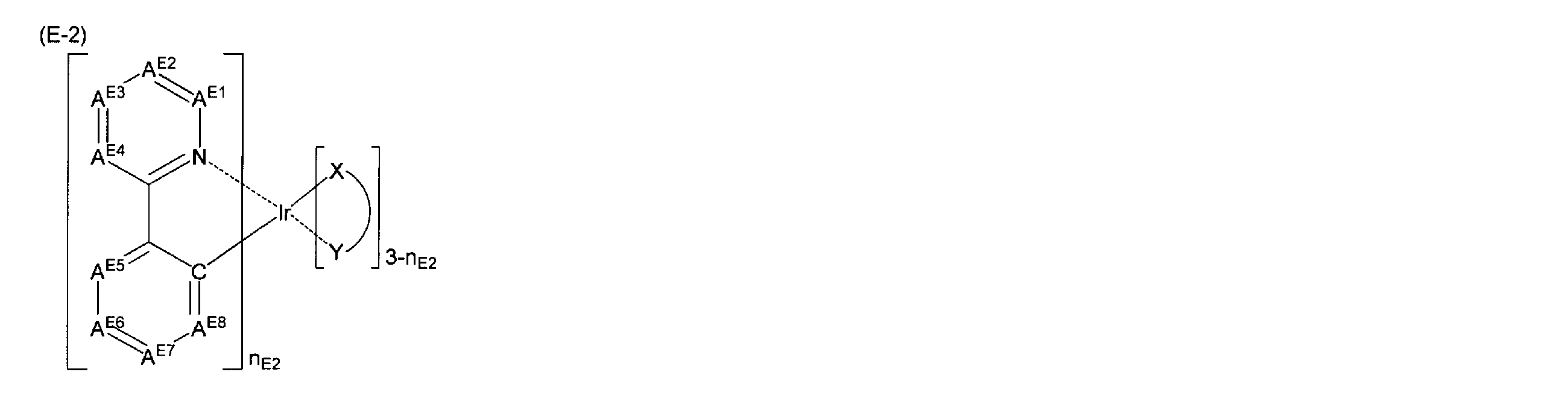
Formula (E-2)
一般式(E-2)中、AE1~AE8はそれぞれ独立に、窒素原子又はC-REを表す。REは水素原子又は置換基を表す。置換基としては、前記置換基群Aとして挙げたものが適用できる。RE同士が互いに連結して環を形成していてもよい。形成される環としては、前述の一般式(E-1)において述べた縮合環と同様のものが挙げられる。(X-Y)及びnE2は一般式(E-1)における(X-Y)及びnE1と同義であり、好ましい範囲も同様である。nE2が2又は3の場合、AE1~AE8を含む配位子が2つまたは3つ存在することになるが、該配位子は互いに同じであっても異なっていても良い。
In general formula (E-2), A E1 to A E8 each independently represents a nitrogen atom or C—R E. R E represents a hydrogen atom or a substituent. As the substituent, those exemplified as the substituent group A can be applied. R E may be connected to each other to form a ring. Examples of the ring formed include the same ring as the condensed ring described in the general formula (E-1). (X-Y) and n E2 is (X-Y) in Formula (E1) have the same meanings as and n E1, preferred ranges are also the same. When n E2 is 2 or 3, there are two or three ligands containing A E1 to A E8, and these ligands may be the same or different.
前記一般式(E-2)で表される化合物のより好ましい形態は、下記一般式(E-3)で表される化合物である。
A more preferred form of the compound represented by the general formula (E-2) is a compound represented by the following general formula (E-3).
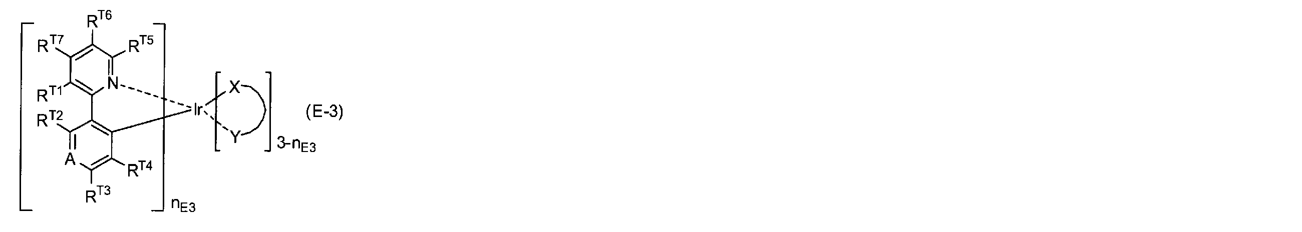
一般式(E-3)中、RT1、RT2、RT3、RT4、RT5、RT6及びRT7は、前記REと同義である。AはCR''''又は窒素原子を表し、R''''は前記REと同義である。RT1~RT7、及びR''''は、近接する任意の2つが互いに結合して縮合4~7員環を形成してもよく、該縮合4~7員環は、シクロアルケン、シクロカルカジエン、アリール又はヘテロアリールであり、該縮合4~7員環は更に置換基群Aで表される置換基を有していてもよい。(X-Y)及びnE3は、一般式(E-1)における(X-Y)及びnE1と同義であり好ましい範囲も同様である。nE3が2又は3の場合、RT1、RT2、RT3、RT4、RT5、RT6、RT7及びAを含む配位子が2つまたは3つ存在することになるが、該配位子は互いに同じであっても異なっていても良い。
In the general formula (E-3), R T1 , R T2 , R T3 , R T4 , R T5 , R T6, and R T7 have the same meaning as R E. A represents CR ″ ″ or a nitrogen atom, and R ″ ″ has the same meaning as RE. R T1 to R T7 and R ″ ″ may be bonded to any two adjacent to each other to form a condensed 4- to 7-membered ring. A fused 4- to 7-membered ring may further have a substituent represented by the substituent group A. (XY) and n E3 have the same meanings as (XY) and n E1 in formula (E-1), and the preferred ranges are also the same. When n E3 is 2 or 3, there are two or three ligands including R T1 , R T2 , R T3 , R T4 , R T5 , R T6 , R T7 and A. The ligands may be the same as or different from each other.
A、RT1~RT7の好ましい範囲は、用途に応じて求められる発光色によって異なる。以下に、目的とする発光色として青色~水色、緑色~黄色、黄橙色~赤色の3つの領域に分けて説明する。ただし、これらの記載に限定されるものではない。
The preferable range of A and R T1 to R T7 varies depending on the emission color required according to the application. In the following, description will be given by dividing into three regions of blue to light blue, green to yellow, yellow orange to red as target emission colors. However, it is not limited to these descriptions.
黄橙色~赤色の発光色を得るためには、下記一般式(E-4)、一般式(E-5)または一般式(E-6)で表される化合物であることが好ましい。
In order to obtain a yellow-orange to red emission color, a compound represented by the following general formula (E-4), general formula (E-5) or general formula (E-6) is preferable.
一般式(E-4)
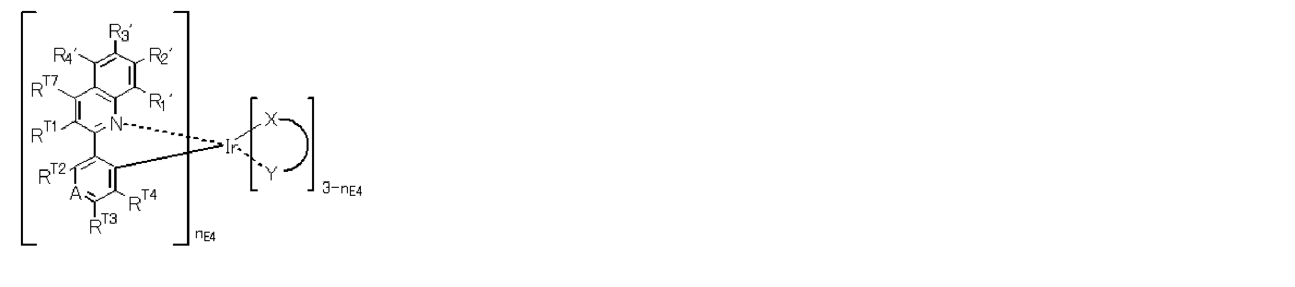
General formula (E-4)
一般式(E-4)におけるRT1~RT4、RT7、A(CR''''又は窒素原子)、(X-Y)及びnE4は、一般式(E-3)におけるRT1~RT4、RT7、A、(X-Y)及びnE3と同義である。R1'~R4'は前記REと同義である。
RT1~RT4、RT7、R1'~R4'、R''''は、近接する任意の2つが互いに結合して縮合4~7員環を形成してもよく、該縮合4~7員環は、シクロアルケン、シクロカルカジエン、アリール又はヘテロアリールであり、該縮合4~7員環は更に置換基群Aで表される置換基有していてもよい。
nE4が2又は3の場合、RT1~RT4、RT7、A及びR1'~R4'を含む配位子が2つまたは3つ存在することになるが、該配位子は互いに同じであっても異なっていても良い。 R T1 to R T4 , R T7 , A (CR ″ ″ or a nitrogen atom), (XY) and n E4 in the general formula (E-4) are R T1 to R T1 in the general formula (E-3). It is synonymous with R T4 , R T7 , A, (XY) and n E3 . R 1 ′ to R 4 ′ have the same meaning as R E.
R T1 to R T4 , R T7 , R 1 ′ to R 4 ′ and R ″ ″ may be bonded to each other to form a condensed 4- to 7-membered ring. The 7-membered ring is cycloalkene, cyclocarbadiene, aryl, or heteroaryl, and the fused 4- to 7-membered ring may further have a substituent represented by Substituent Group A.
When n E4 is 2 or 3, there are two or three ligands including R T1 to R T4 , R T7 , A and R 1 ′ to R 4 ′. They may be the same or different.
R1'~R4'は、水素原子、フッ素原子、アルキル基、アリール基であることが好ましい。また、AがCR''''を表すと共に、RT1~RT4、RT7、R''''のうち0~3つがアルキル基又はフェニル基で残りが全て水素原子である場合が好ましい。
R 1 ′ to R 4 ′ are preferably a hydrogen atom, a fluorine atom, an alkyl group, or an aryl group. Further, it is preferable that A represents CR ″ ″, and 0 to 3 of R T1 to R T4 , R T7 and R ″ ″ are an alkyl group or a phenyl group, and the rest are all hydrogen atoms.
一般式(E-4)で表される化合物の好ましい具体例を以下に列挙するが、以下に限定されるものではない。

Preferred specific examples of the compound represented by the general formula (E-4) are listed below, but are not limited thereto.
一般式(E-5)
General formula (E-5)

一般式(E-5)におけるRT2~RT6、A(CR''''又は窒素原子)、(X-Y)及びnE5は、一般式(E-3)におけるRT2~RT6、A、(X-Y)及びnE3と同義である。R5'~R8'は一般式(E-4)におけるR1'~R4'と同義である。 RT2~RT6、R5'~R8'、 R''''は、近接する任意の2つが互いに結合して縮合4~7員環を形成してもよく、該縮合4~7員環は、シクロアルケン、シクロカルカジエン、アリール又はヘテロアリールであり、該縮合4~7員環は更に置換基群Aで表される置換基を有していてもよい。
nE5が2又は3の場合、RT2~RT6、A及びR5'~R8'を含む配位子が2つまたは3つ存在することになるが、該配位子は互いに同じであっても異なっていても良い。
また、R5'~R8'における好ましい範囲は、一般式(E-4)におけるR1'~R4'の好ましい範囲と同じである。またAがCR''''を表すと共に、RT2~RT6、R''''、及びR5'~R8'のうち、0~3つがアルキル基又はフェニル基で残りが全て水素原子である場合が好ましい。 R T2 to R T6 , A (CR ″ ″ or nitrogen atom), (XY) and n E5 in the general formula (E-5) are R T2 to R T6 in the general formula (E-3), Synonymous with A, (XY) and n E3 . R 5 ′ to R 8 ′ have the same meanings as R 1 ′ to R 4 ′ in formula (E-4). R T2 to R T6 , R 5 ′ to R 8 ′, and R ″ ″ may be bonded to each other to form a condensed 4- to 7-membered ring. The ring is a cycloalkene, cyclocarbadiene, aryl or heteroaryl, and the condensed 4- to 7-membered ring may further have a substituent represented by the substituent group A.
When n E5 is 2 or 3, there are two or three ligands containing R T2 to R T6 , A and R 5 ′ to R 8 ′. It can be different.
The preferred range for R 5 ′ to R 8 ′ is the same as the preferred range for R 1 ′ to R 4 ′ in formula (E-4). A represents CR ″ ″, and among R T2 to R T6 , R ″ ″, and R 5 ′ to R 8 ′, 0 to 3 are alkyl groups or phenyl groups, and the rest are all hydrogen atoms. Is preferred.
一般式(E-5)で表される化合物の好ましい具体例を以下に列挙するが、以下に限定されるものではない。
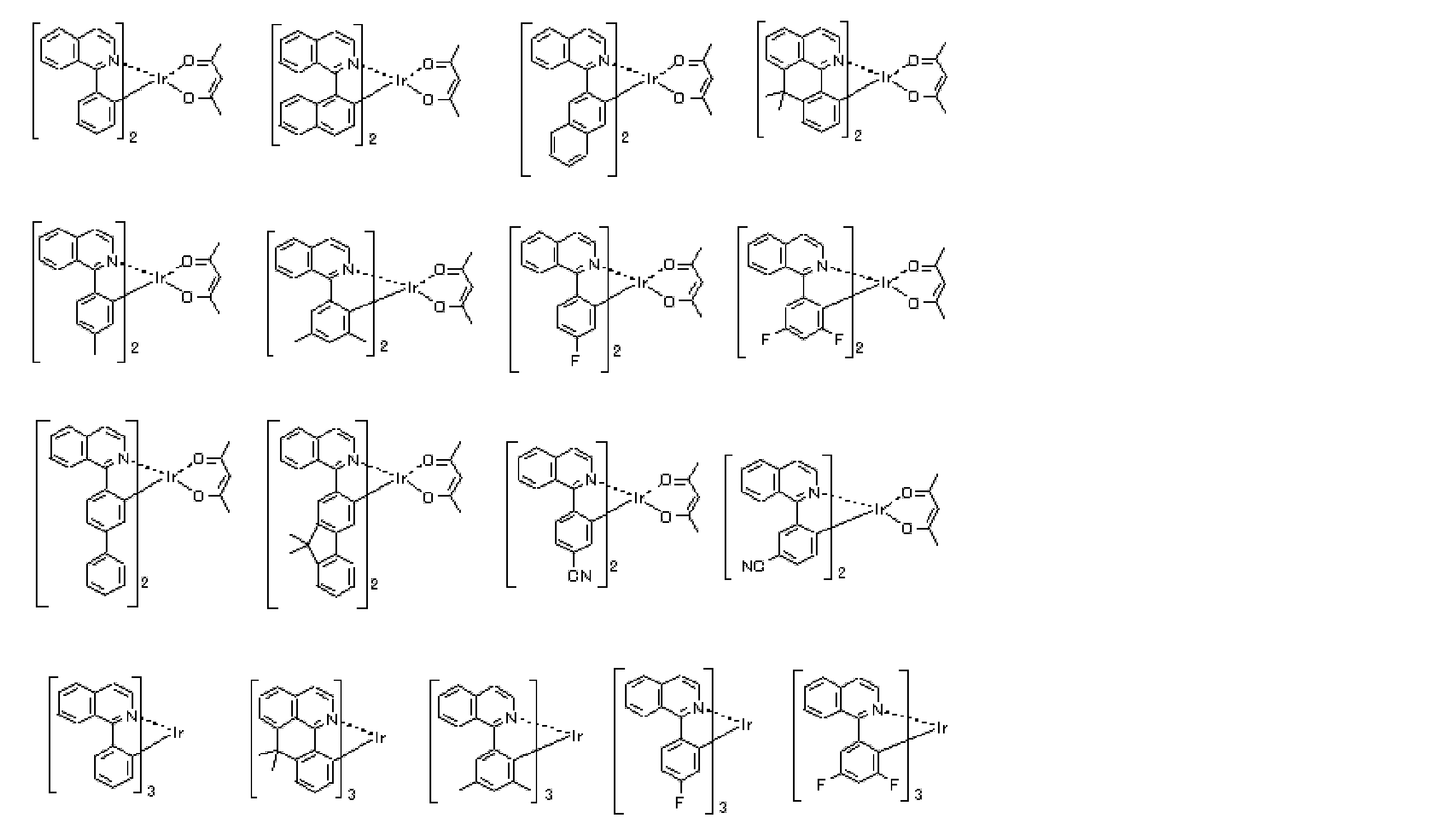
Preferred specific examples of the compound represented by formula (E-5) are listed below, but are not limited thereto.
一般式(E-6)
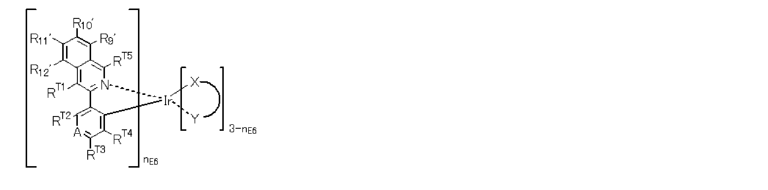
General formula (E-6)
一般式(E-6)におけるRT1~RT5、A(CR''''又は窒素原子)、(X-Y)及びnE6は、一般式(E-3)におけるRT1~RT5、A、(X-Y)及びnE3と同義である。R9'~R12'は一般式(E-4)におけるR1'~R4'と同義である。RT1~RT5、R9'~R12'、 R''''は、近接する任意の2つが互いに結合して縮合4~7員環を形成してもよく、該縮合4~7員環は、シクロアルケン、シクロカルカジエン、アリール又はヘテロアリールであり、該縮合4~7員環は更に置換基群Aで表される置換基を有していてもよい。
nE6が2又は3の場合、RT1~RT5、A及びR9'~R12'を含む配位子が2つまたは3つ存在することになるが、該配位子は互いに同じであっても異なっていても良い。
また、R9'~R12'における好ましい範囲は、一般式(E-4)におけるR1'~R4'の好ましい範囲と同じである。またAがCR''''を表すと共に、RT1~RT5、R''''、及びR9'~R12'のうち、0~3つがアルキル基又はフェニル基で残りが全て水素原子である場合が好ましい。 R T1 to R T5 , A (CR ″ ″ or nitrogen atom), (XY) and n E6 in the general formula (E-6) are R T1 to R T5 in the general formula (E-3), Synonymous with A, (XY) and n E3 . R 9 ′ to R 12 ′ have the same meanings as R 1 ′ to R 4 ′ in formula (E-4). R T1 to R T5 , R 9 ′ to R 12 ′, and R ″ ″ may be bonded to each other to form a condensed 4- to 7-membered ring. The ring is a cycloalkene, cyclocarbadiene, aryl or heteroaryl, and the condensed 4- to 7-membered ring may further have a substituent represented by the substituent group A.
When n E6 is 2 or 3, there are two or three ligands containing R T1 to R T5 , A and R 9 ′ to R 12 ′. It can be different.
The preferred range for R 9 ′ to R 12 ′ is the same as the preferred range for R 1 ′ to R 4 ′ in formula (E-4). A represents CR ″ ″, and among R T1 to R T5 , R ″ ″, and R 9 ′ to R 12 ′, 0 to 3 are alkyl groups or phenyl groups, and the rest are all hydrogen atoms. Is preferred.
一般式(E-6)で表される化合物の好ましい具体例を以下に列挙するが、以下に限定されるものではない。
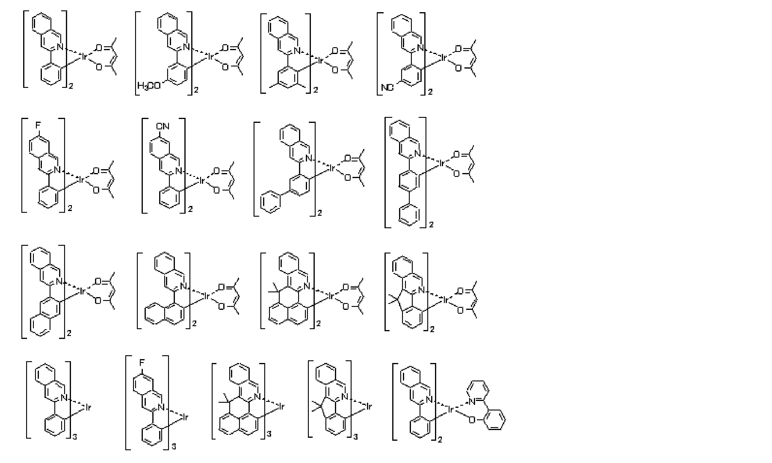
Preferred specific examples of the compound represented by formula (E-6) are listed below, but are not limited thereto.
緑色~黄色の発光色を得るためには、下記一般式(E-7)で表される化合物であることが好ましい。
In order to obtain a green to yellow emission color, a compound represented by the following general formula (E-7) is preferable.
一般式(E-7)
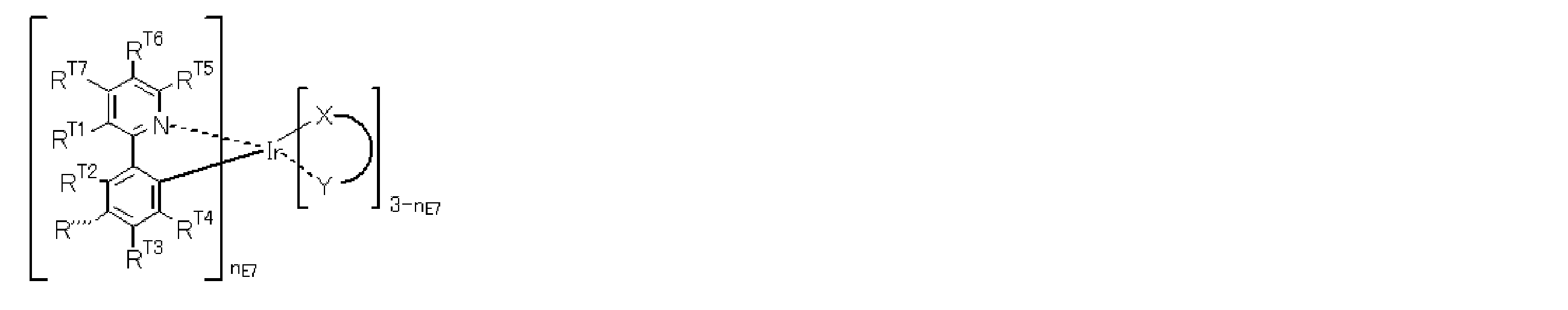
一般式(E-7)中、RT1、RT2、RT3、RT4、RT5、RT6、RT7、R''''、(X-Y)及びnE3は一般式(E-3)中のRT1、RT2、RT3、RT4、RT5、RT6、RT7、R''''、(X-Y)及びnE3と同義である。RT1~RT7、及びR''''は、近接する任意の2つが互いに結合して縮合4~7員環を形成してもよく、該縮合4~7員環は、シクロアルケン、シクロカルカジエン、アリール又はヘテロアリールであり、該縮合4~7員環は更に置換基群Aで表される置換基を有していてもよい。
nE7が2又は3の場合、RT1、RT2、RT3、RT4、RT5、RT6、RT7及びR''''を含む配位子が2つまたは3つ存在することになるが、該配位子は互いに同じであっても異なっていても良い。 General formula (E-7)
In the general formula (E-7), R T1 , R T2 , R T3 , R T4 , R T5 , R T6 , R T7 , R ″ ″, (XY) and n E3 are represented by the general formula (E− It is synonymous with R T1 , R T2 , R T3 , R T4 , R T5 , R T6 , R T7 , R ″ ″, (XY) and n E3 in 3 ). R T1 to R T7 and R ″ ″ may be bonded to any two adjacent to each other to form a condensed 4- to 7-membered ring. A fused 4- to 7-membered ring may further have a substituent represented by the substituent group A.
When n E7 is 2 or 3, there are two or three ligands including R T1 , R T2 , R T3 , R T4 , R T5 , R T6 , R T7 and R ″ ″. However, the ligands may be the same or different from each other.
nE7が2又は3の場合、RT1、RT2、RT3、RT4、RT5、RT6、RT7及びR''''を含む配位子が2つまたは3つ存在することになるが、該配位子は互いに同じであっても異なっていても良い。 General formula (E-7)
When n E7 is 2 or 3, there are two or three ligands including R T1 , R T2 , R T3 , R T4 , R T5 , R T6 , R T7 and R ″ ″. However, the ligands may be the same or different from each other.
RT1、RT2、RT3、RT4、RT5、RT6、RT7、R''''は、水素原子、フッ素原子、アルキル基、アリール基、ヘテロアリール基、シアノ基であることが好ましい。
R T1 , R T2 , R T3 , R T4 , R T5 , R T6 , R T7 , R ″ ″ may be a hydrogen atom, a fluorine atom, an alkyl group, an aryl group, a heteroaryl group, or a cyano group preferable.
nE7は3であることが好ましく、さらに、一般式(E-7)は一般式(E-7-1)で表される化合物であることが好ましい。
n E7 is preferably 3, and the general formula (E-7) is preferably a compound represented by the general formula (E-7-1).
一般式(E-7-1)
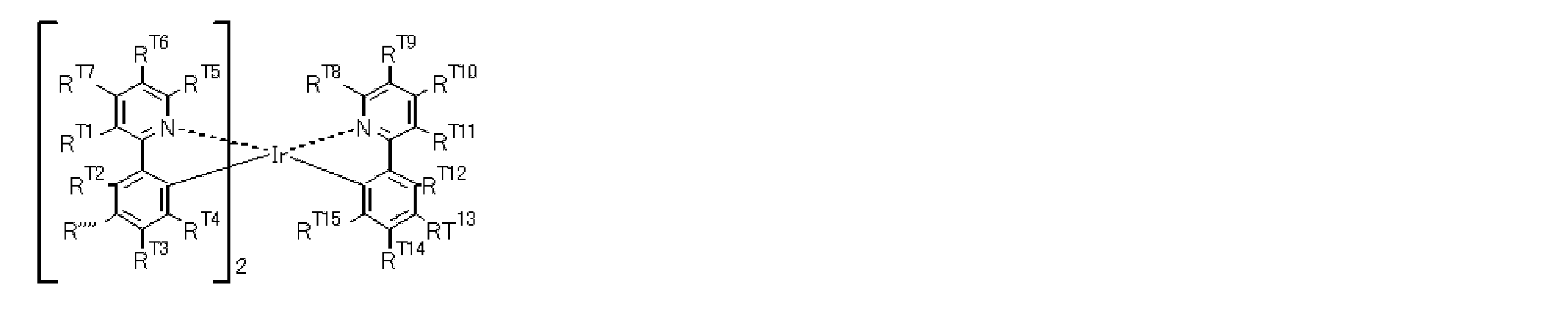
一般式(E-7-1)中、RT1、RT2、RT3、RT4、RT5、RT6、RT7、R''''は一般式(E-7)中のRT1、RT2、RT3、RT4、RT5、RT6、RT7、R''''と同義であり好ましい範囲も同じである。RT8~RT15はRT1、RT2、RT3、RT4、RT5、RT6、RT7、R''''と同義であり好ましい範囲も同じであるが、RT1、RT2、RT3、RT4、RT5、RT6、RT7、R''''を含むフェニルピリジン配位子とRT8~RT15を含むフェニルピリジン配位子は互いに異なる。
Formula (E-7-1)
In the general formula (E-7-1), R T1 , R T2 , R T3 , R T4 , R T5 , R T6 , R T7 , R ″ ″ are R T1 in the general formula (E-7), R T2 , R T3 , R T4 , R T5 , R T6 , R T7 , R ″ ″ have the same meanings and preferred ranges. R T8 to R T15 are synonymous with R T1 , R T2 , R T3 , R T4 , R T5 , R T6 , R T7 , R ″ ″ and the preferred ranges are also the same, but R T1 , R T2 , A phenylpyridine ligand containing R T3 , R T4 , R T5 , R T6 , R T7 , R ″ ″ and a phenylpyridine ligand containing R T8 to R T15 are different from each other.
緑色~黄色の発光色のうち、緑色に近い発光色を得るためには、RT1、RT2、RT3、RT4、RT5、RT6、RT7、R''''は水素原子、フッ素原子、アルキル基、シアノ基であることがより好ましく、RT1、RT5、RT4、R''''の1~3個がアルキル基であることがさらに好ましい。RT8~RT11は水素原子またはアルキル基であることがより好ましい。また、RT12~RT15は水素原子、アルキル基、シアノ基、アリール基であることがより好ましい。アルキル基、シアノ基、アリール基の置換位置としては、RT13またはRT14であることが好ましい。該アリール基は、さらに置換基を有していてもよく、置換基を介して縮合環を形成してもよい。
In order to obtain an emission color close to green among green to yellow emission colors, R T1 , R T2 , R T3 , R T4 , R T5 , R T6 , R T7 , R ″ ″ are hydrogen atoms, A fluorine atom, an alkyl group, and a cyano group are more preferable, and 1 to 3 of R T1 , R T5 , R T4 , and R ″ ″ are more preferably an alkyl group. R T8 to R T11 are more preferably a hydrogen atom or an alkyl group. R T12 to R T15 are more preferably a hydrogen atom, an alkyl group, a cyano group, or an aryl group. The substitution position of the alkyl group, cyano group or aryl group is preferably R T13 or R T14 . The aryl group may further have a substituent, and may form a condensed ring through the substituent.
緑色~黄色の発光色のうち、黄色に近い発光色を得るためには、RT1、RT2、RT3、RT4、RT5、RT6、RT7、R''''は水素原子、アルキル基であることがより好ましく、RT1、RT5、RT4、R''''の1~3個がアルキル基であることがさらに好ましい。RT8~RT11は少なくとも1つがアリール基であることがより好ましく、RT9、RT10のいずれか1つがアリール基で残りは水素原子またはアルキル基であることがさらに好ましい。該アリール基は、さらに置換基を有していてもよく、置換基を介して縮合環を形成してもよい。
In order to obtain an emission color close to yellow among green to yellow emission colors, R T1 , R T2 , R T3 , R T4 , R T5 , R T6 , R T7 , R ″ ″ are hydrogen atoms, It is more preferably an alkyl group, and more preferably 1 to 3 of R T1 , R T5 , R T4 and R ″ ″ are alkyl groups. It is more preferable that at least one of R T8 to R T11 is an aryl group, and it is more preferable that any one of R T9 and R T10 is an aryl group and the remaining is a hydrogen atom or an alkyl group. The aryl group may further have a substituent, and may form a condensed ring through the substituent.
一般式(E-7-1)は、一般式(E-7-1)中に一般式(E-7-2)で表される部分構造を有することも好ましい。一般式(E-7-2)を有することにより、ホスト材料との組み合わせによって低電圧化や高耐久化といった効果が顕著に現れる場合がある。
The general formula (E-7-1) preferably has a partial structure represented by the general formula (E-7-2) in the general formula (E-7-1). By having the general formula (E-7-2), effects such as low voltage and high durability may be noticeable depending on the combination with the host material.
一般式(E-7-2)
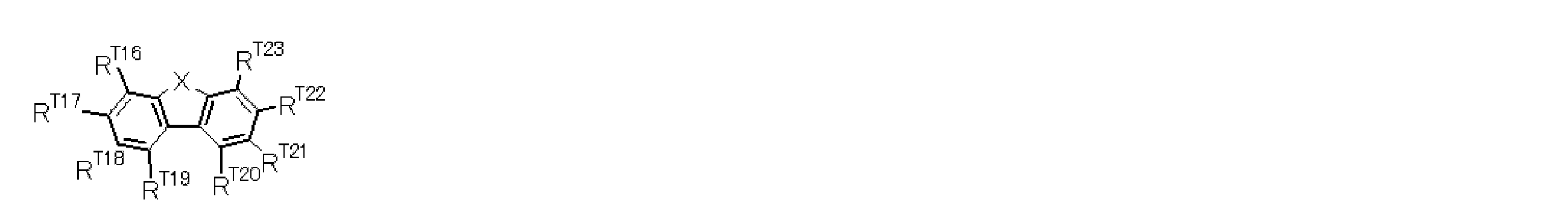
一般式(E-7-2)中、Xは-O-,-S-、-NRT24-、-CRT25RT26-、-SiRT27RT28-であり、RT16~RT28のいずれか一つが単結合または置換基を介して一般式(E-7-1)中の一部と結合する。
General formula (E-7-2)
In general formula (E-7-2), X represents —O—, —S—, —NR T24 —, —CR T25 R T26 —, —SiR T27 R T28 —, and any one of R T16 to R T28 One is bonded to part of the general formula (E-7-1) through a single bond or a substituent.
一般式(E-7-2)中、RT16~RT28のいずれか一つが単結合もしくはアリール基を介して一般式(E-7-1)中の一部と結合することが好ましく、緑色に近い発光色を得たい場合にはRT13またはRT14で結合することがより好ましく、RT13で結合することがさらに好ましい。黄色に近い発光色を得たい場合にはRT9またはRT10で結合することがより好ましい。
Xは-O-,-S-、-NRT24-、-CRT25RT26-であることが好ましく、-O-,-S-であることがより好ましい。
Xが-O-,-S-のときは、RT16の位置で単結合を介して一般式(E-7-1)中の一部と結合することが好ましく、Xが-NRT24-のときは、RT18またはRT24の位置で単結合を介して一般式(E-7-1)中の一部と結合することが好ましく、Xが-CRT25RT26-のときは、RT17の位置で単結合を介して一般式(E-7-1)中の一部と結合することが好ましい。 In general formula (E-7-2), any one of R T16 to R T28 is preferably bonded to a part of general formula (E-7-1) via a single bond or an aryl group, When it is desired to obtain a light emission color close to, it is more preferable to bond with R T13 or R T14 , and further preferable to bond with R T13 . When it is desired to obtain a light emission color close to yellow, it is more preferable to bond with R T9 or R T10 .
X is preferably —O—, —S—, —NR T24 —, —CR T25 R T26 —, and more preferably —O—, —S—.
When X is —O— or —S—, it is preferably bonded to a part of formula (E-7-1) through a single bond at the position of R T16 , and X is —NR T24 — In this case, it is preferable to bond to a part of the general formula (E-7-1) through a single bond at the position of R T18 or R T24 , and when X is —CR T25 R T26 —, R T17 It is preferable to bond to a part of the general formula (E-7-1) through a single bond at the position.
一般式(E-7)で表される化合物の好ましい具体例を以下に列挙するが、以下に限定されるものではない。
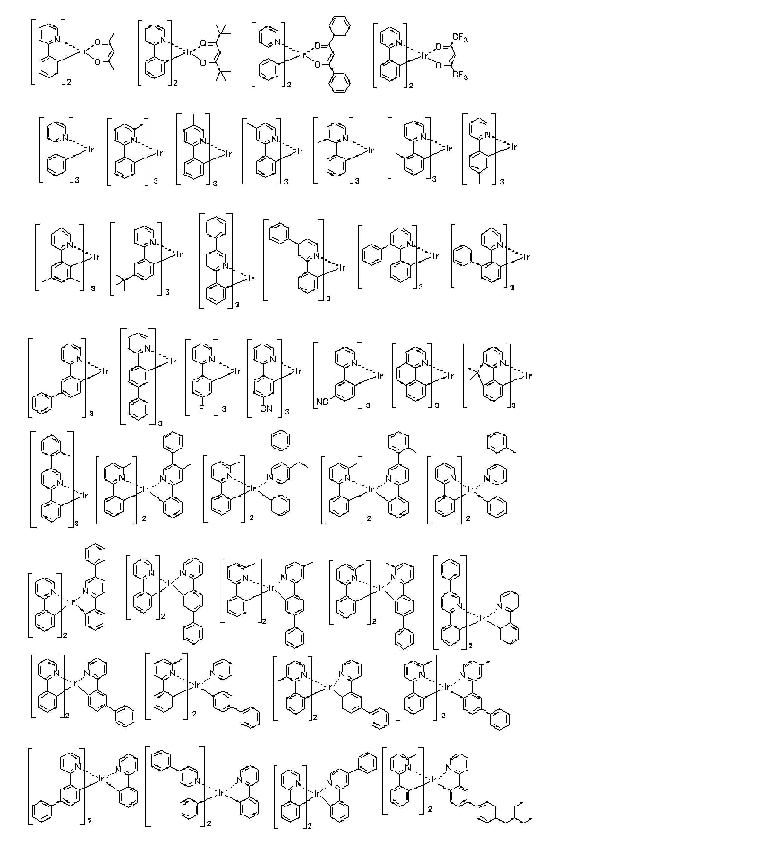
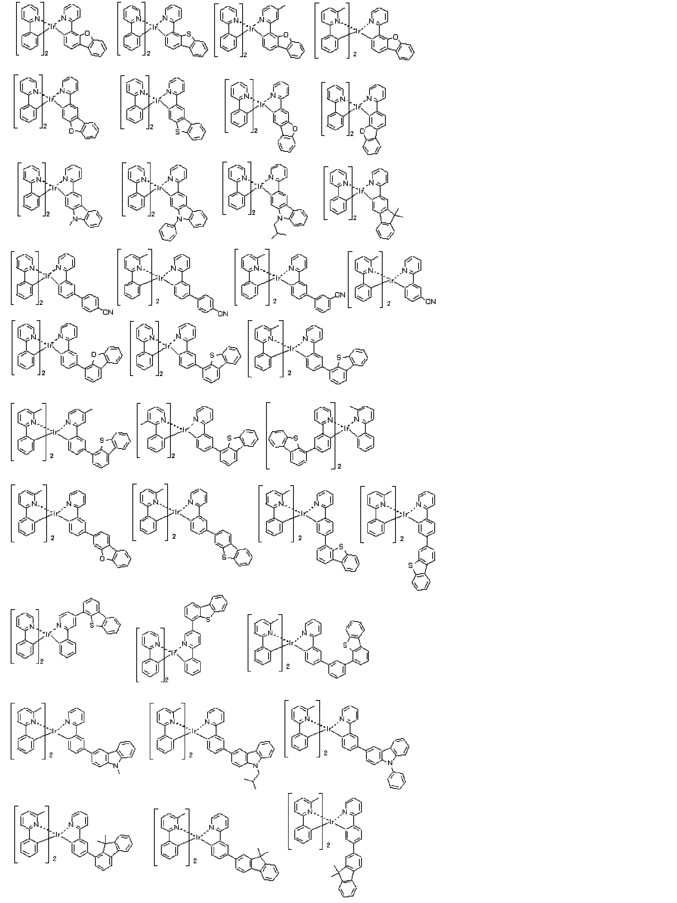
Preferred specific examples of the compound represented by formula (E-7) are listed below, but are not limited thereto.
青色~水色の発光色を得るためには、下記一般式(E-8)または一般式(E-9)で表される化合物であることが好ましい。
In order to obtain a blue to light blue luminescent color, a compound represented by the following general formula (E-8) or general formula (E-9) is preferable.
一般式(E-8)
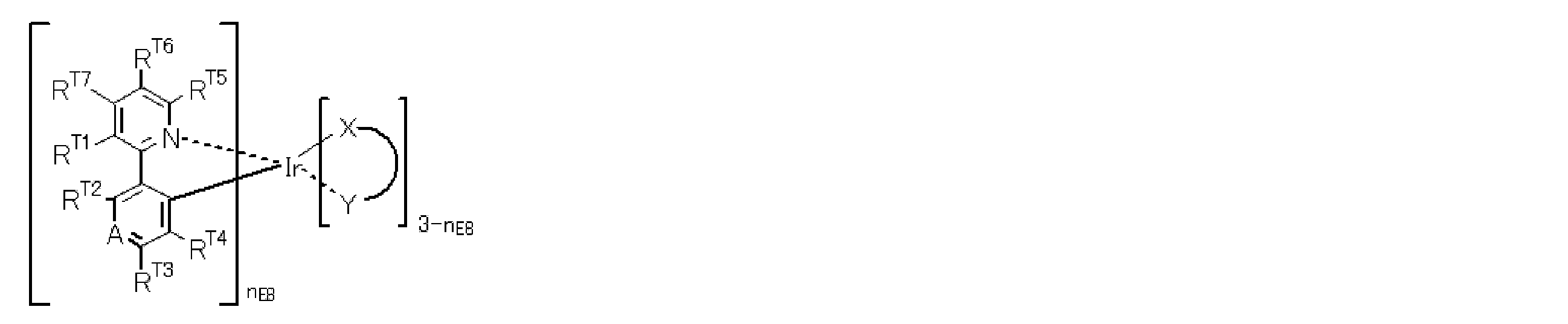
General formula (E-8)
一般式(E-8)中、RT1、RT2、RT3、RT4、RT5、RT6、RT7、A(CR''''又は窒素原子)、(X-Y)、nE8は一般式(E-3)中のRT1、RT2、RT3、RT4、RT5、RT6、RT7、A、(X-Y)、nE3と同義である。
In general formula (E-8), R T1 , R T2 , R T3 , R T4 , R T5 , R T6 , R T7 , A (CR ″ ″ or nitrogen atom), (XY), n E8 Is synonymous with R T1 , R T2 , R T3 , R T4 , R T5 , R T6 , R T7 , A, (XY), and n E3 in the general formula (E-3).
一般式(E-8)中のRT1、RT5~RT7は、水素原子、アルキル基、アリール基であることがより好ましい。RT2~RT4は、水素原子、フッ素原子、シアノ基であることが好ましい。Aは、CR''''のR''''がフッ素原子もしくはシアノ基であるか又は窒素原子であるかのいずれかが好ましい。nE8は2又は3であることが好ましくい。(X-Y)は、一般式(E-1)における(X-Y)と同義であり好ましい範囲も同様である。
In general formula (E-8), R T1 and R T5 to R T7 are more preferably a hydrogen atom, an alkyl group, or an aryl group. R T2 to R T4 are preferably a hydrogen atom, a fluorine atom, or a cyano group. In A, R ″ ″ of CR ″ ″ is preferably a fluorine atom or a cyano group, or a nitrogen atom. n E8 is preferably 2 or 3. (XY) has the same meaning as (XY) in formula (E-1), and the preferred range is also the same.
一般式(E-8)で表される化合物の好ましい具体例を以下に列挙するが、以下に限定されるものではない。
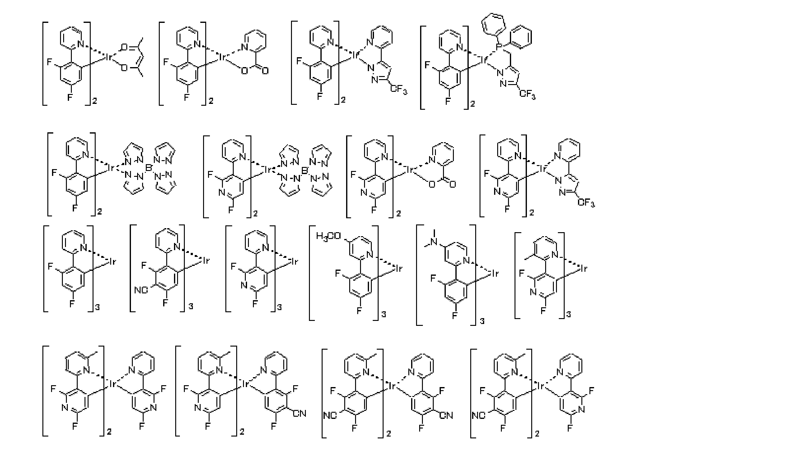
Preferred specific examples of the compound represented by formula (E-8) are listed below, but are not limited thereto.
一般式(E-9)
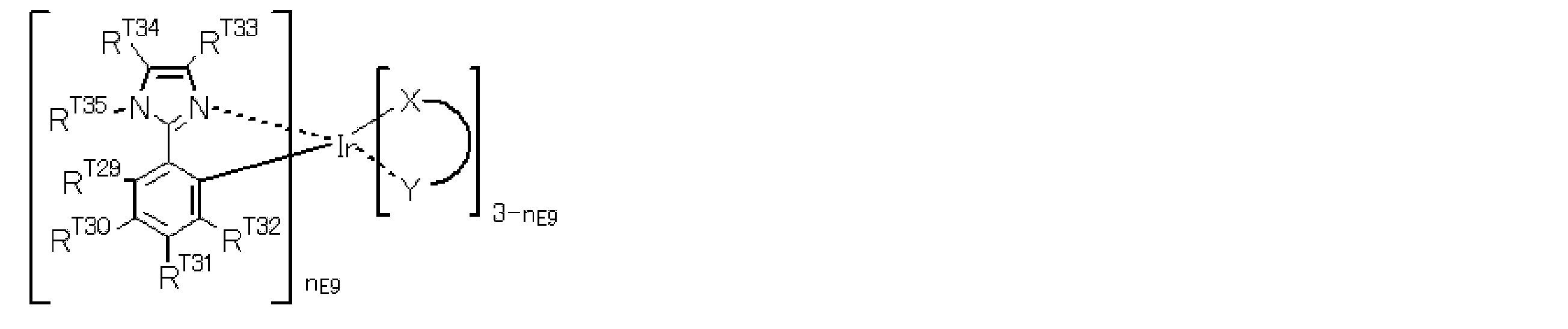
一般式(E-9)中、RT29~RT34、(X-Y)、nE8は一般式(E-3)中のRT1~RT6(X-Y)、nE3と同義である。RT35は置換基を表し、該置換基としては前記置換基群Bが挙げられる。RT29~RT35は、近接する任意の2つが互いに結合して縮合4~7員環を形成してもよく、該縮合4~7員環は、シクロアルケン、シクロカルカジエン、アリール又はヘテロアリールであり、該縮合4~7員環は更に置換基群Aで表される置換基を有していてもよい。
nE7が2又は3の場合、RT1、RT2、RT3、RT4、RT5、RT6、RT7及びR''''を含む配位子が2つまたは3つ存在することになるが、該配位子は互いに同じであっても異なっていても良い。 General formula (E-9)
In the general formula (E-9), R T29 to R T34 , (XY), and n E8 have the same meanings as R T1 to R T6 (XY) and n E3 in the general formula (E-3). . R T35 represents a substituent, and examples of the substituent include the substituent group B. R T29 to R T35 may combine any two adjacent to each other to form a condensed 4- to 7-membered ring, and the fused 4- to 7-membered ring is a cycloalkene, cyclocarbadiene, aryl or heteroaryl The condensed 4- to 7-membered ring may further have a substituent represented by the substituent group A.
When n E7 is 2 or 3, there are two or three ligands including R T1 , R T2 , R T3 , R T4 , R T5 , R T6 , R T7 and R ″ ″. However, the ligands may be the same or different from each other.
nE7が2又は3の場合、RT1、RT2、RT3、RT4、RT5、RT6、RT7及びR''''を含む配位子が2つまたは3つ存在することになるが、該配位子は互いに同じであっても異なっていても良い。 General formula (E-9)
When n E7 is 2 or 3, there are two or three ligands including R T1 , R T2 , R T3 , R T4 , R T5 , R T6 , R T7 and R ″ ″. However, the ligands may be the same or different from each other.
RT29~RT34は水素原子、アルキル基、アリール基、シアノ基であることが好ましい。RT35はアルキル基、アリール基であることが好ましい。RT35はRT29と連結して環を形成することが好ましく、RT35とRT29とがアリール基を介して結合し、その結果含窒素6員環が形成されることがより好ましい。RT35はRT29と連結した該アリール基はさらに置換基を有していてもよく、耐久性の観点からアルキル基によって置換されることがさらに好ましい。
R T29 to R T34 are preferably a hydrogen atom, an alkyl group, an aryl group, or a cyano group. R T35 is preferably an alkyl group or an aryl group. R T35 is preferably linked to R T29 to form a ring, and R T35 and R T29 are more preferably bonded via an aryl group, resulting in the formation of a nitrogen-containing 6-membered ring. In R T35, the aryl group linked to R T29 may further have a substituent, and is more preferably substituted with an alkyl group from the viewpoint of durability.
一般式(E-9)で表される化合物の好ましい具体例を以下に列挙するが、以下に限定されるものではない。
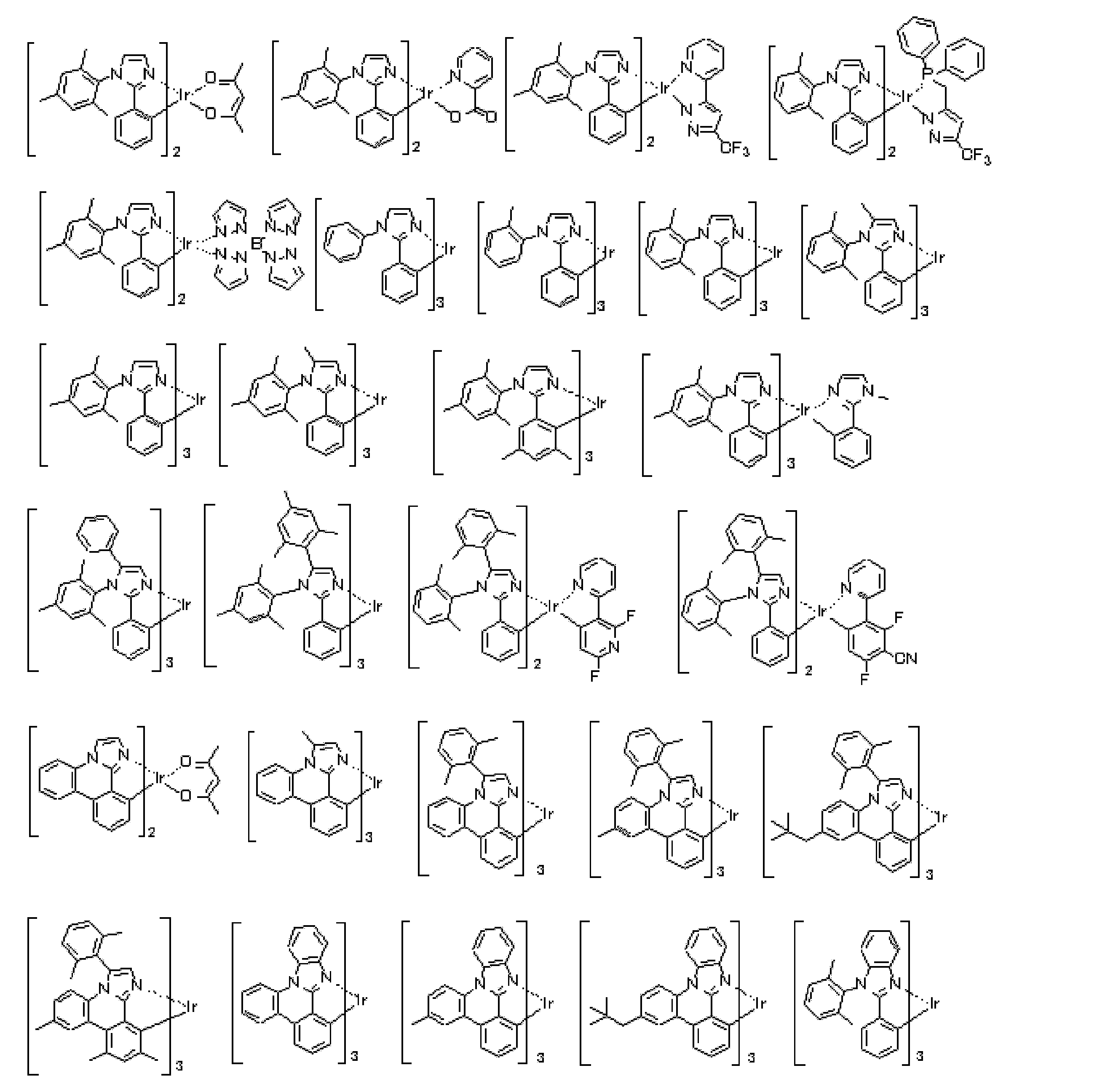
Preferred specific examples of the compound represented by formula (E-9) are listed below, but are not limited thereto.
一般式(E-1)で表される化合物の上記以外の好ましい具体例を以下に列挙するが、以下に限定されるものではない。
Preferred specific examples other than the above of the compound represented by the general formula (E-1) are listed below, but are not limited thereto.
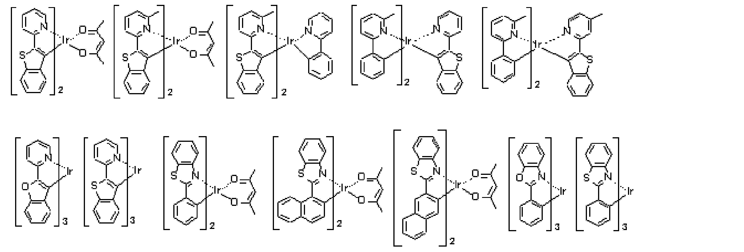
上記一般式(E-1)で表される化合物として例示した化合物は、特開2009-99783号公報に記載の方法や、米国特許7279232号等に記載の種々の方法で合成できる。合成後、カラムクロマトグラフィー、再結晶等による精製を行った後、昇華精製により精製することが好ましい。昇華精製により、有機不純物を分離できるだけでなく、無機塩や残留溶媒等を効果的に取り除くことができる。
The compounds exemplified as the compound represented by the general formula (E-1) can be synthesized by the method described in JP2009-99783A, various methods described in US Pat. No. 7,279,232 and the like. After synthesis, it is preferable to purify by sublimation purification after purification by column chromatography, recrystallization or the like. By sublimation purification, not only can organic impurities be separated, but inorganic salts and residual solvents can be effectively removed.
一般式(E-1)で表される化合物は、発光層に含有されることが好ましいが、その用途が限定されることはなく、更に有機層内のいずれの層に更に含有されてもよい。
The compound represented by the general formula (E-1) is preferably contained in the light emitting layer, but its use is not limited, and may be further contained in any layer in the organic layer. .
発光層中の一般式(E-1)で表される化合物は,発光層中に一般的に発光層を形成する全化合物質量に対して、0.1質量%~50質量%含有されるが、耐久性、外部量子効率の観点から0.2質量%~50質量%含有されることが好ましく、0.3質量%~40質量%含有されることがより好ましく、0.4質量%~30質量%含有されることがさらに好ましく、0.5質量%~20質量%含有されることが特に好ましい。
The compound represented by the general formula (E-1) in the light emitting layer is generally contained in the light emitting layer in an amount of 0.1% by mass to 50% by mass with respect to the total mass of the compound forming the light emitting layer. From the viewpoint of durability and external quantum efficiency, the content is preferably 0.2% by mass to 50% by mass, more preferably 0.3% by mass to 40% by mass, and more preferably 0.4% by mass to 30%. More preferably, it is contained in an amount of 0.5% by mass to 20% by mass.
一般式(1)で表される化合物、一般式(3-A)で表される部分構造、部分構造群(1A)と、一般式(E-1)~(E-9)のいずれかで表される化合物を発光層中で組み合わせて使用することが、本発明では特に好ましい。
A compound represented by the general formula (1), a partial structure represented by the general formula (3-A), a partial structure group (1A), and any one of the general formulas (E-1) to (E-9) It is particularly preferable in the present invention to use the compounds represented in combination in the light emitting layer.
前記白金(Pt)錯体として具体的には、特開2005-310733号公報の〔0143〕~〔0152〕、〔0157〕~〔0158〕、〔0162〕~〔0168〕に記載の化合物、特開2006-256999号公報の〔0065〕~〔0083〕に記載の化合物、特開2006-93542号公報の〔0065〕~〔0090〕に記載の化合物、特開2007-73891号公報の〔0063〕~〔0071〕に記載の化合物、特開2007-324309号公報の〔0079〕~〔0083〕に記載の化合物、特開2006-93542号公報の〔0065〕~〔0090〕に記載の化合物、特開2007-96255号公報の〔0055〕~〔0071〕に記載の化合物、特開2006-313796号公報の〔0043〕~〔0046〕が挙げられる。
Specific examples of the platinum (Pt) complex include compounds described in [0143] to [0152], [0157] to [0158], and [0162] to [0168] of JP-A No. 2005-310733, Compounds described in [0065] to [0083] of 2006-256999, compounds described in [0065] to [0090] of JP-A-2006-93542, and [0063] to [0063] of JP-A-2007-73491 Compounds described in [0071], compounds described in [0079] to [0083] of JP-A-2007-324309, compounds described in [0065] to [0090] of JP-A-2006-93542, JP-A Compounds described in [0055] to [0071] of 2007-96255, [0043] of JP-A-2006-313796 [0046] and the like.
燐光発光材料として用いることができる白金(Pt)錯体として好ましくは、下記一般式(C-1)で表される白金(Pt)錯体である。
The platinum (Pt) complex that can be used as the phosphorescent material is preferably a platinum (Pt) complex represented by the following general formula (C-1).

(式中、Q1、Q2、Q3及びQ4はそれぞれ独立に白金(Pt)に配位する配位子を表す。L1、L2及びL3はそれぞれ独立に単結合又は二価の連結基を表す。)
(In the formula, Q 1 , Q 2 , Q 3 and Q 4 each independently represent a ligand coordinated to platinum (Pt). L 1 , L 2 and L 3 are each independently a single bond or a divalent group. Represents a linking group.)
一般式(C-1)について説明する。Q1、Q2、Q3及びQ4はそれぞれ独立に白金(Pt)に配位する配位子を表す。この時、Q1、Q2、Q3及びQ4と白金(Pt)の結合は、共有結合、イオン結合、配位結合などいずれであっても良い。Q1、Q2、Q3及びQ4中の白金(Pt)に結合する原子としては、炭素原子、窒素原子、酸素原子、硫黄原子、リン原子が好ましく、Q1、Q2、Q3及びQ4中の白金(Pt)に結合する原子の内、少なくとも一つが炭素原子であることが好ましく、二つが炭素原子であることがより好ましく、二つが炭素原子で、二つが窒素原子であることが特に好ましい。
炭素原子で白金(Pt)に結合するQ1、Q2、Q3及びQ4としては、アニオン性の配位子でも中性の配位子でもよく、アニオン性の配位子としてはビニル配位子、芳香族炭化水素環配位子(例えばベンゼン配位子、ナフタレン配位子、アントラセン配位子、フェナントレン配位子など)、ヘテロ環配位子(例えばフラン配位子、チオフェン配位子、ピリジン配位子、ピラジン配位子、ピリミジン配位子、ピリダジン配位子、トリアジン配位子、チアゾール配位子、オキサゾール配位子、ピロール配位子、イミダゾール配位子、ピラゾール配位子、トリアゾール配位子及び、それらを含む縮環体(例えばキノリン配位子、ベンゾチアゾール配位子など))が挙げられる。中性の配位子としてはカルベン配位子が挙げられる。 The general formula (C-1) will be described. Q 1 , Q 2 , Q 3 and Q 4 each independently represent a ligand coordinated to platinum (Pt). At this time, the bond between Q 1 , Q 2 , Q 3 and Q 4 and platinum (Pt) may be any of a covalent bond, an ionic bond, a coordinate bond, and the like. As an atom couple | bonded with platinum (Pt) in Q < 1 >, Q < 2 >, Q < 3 > and Q < 4 >, a carbon atom, a nitrogen atom, an oxygen atom, a sulfur atom, and a phosphorus atom are preferable, Q < 1 >, Q < 2 >, Q < 3 > Of the atoms bonded to platinum (Pt) in Q 4 , at least one is preferably a carbon atom, more preferably two are carbon atoms, two are carbon atoms, and two are nitrogen atoms. Is particularly preferred.
Q 1 , Q 2 , Q 3, and Q 4 bonded to platinum (Pt) by a carbon atom may be an anionic ligand or a neutral ligand, and the anionic ligand is a vinyl group. Ligand, aromatic hydrocarbon ring ligand (eg benzene ligand, naphthalene ligand, anthracene ligand, phenanthrene ligand, etc.), heterocyclic ligand (eg furan ligand, thiophene coordination) Pyridine ligand, pyrazine ligand, pyrimidine ligand, pyridazine ligand, triazine ligand, thiazole ligand, oxazole ligand, pyrrole ligand, imidazole ligand, pyrazole coordination Child, a triazole ligand, and a condensed ring containing them (for example, quinoline ligand, benzothiazole ligand, etc.). A carbene ligand is mentioned as a neutral ligand.
Q1、Q2、Q3及びQ4で表される基は、置換基を有していてもよく、置換基としては前記置換基群Aとして挙げたものが適宜適用できる。また置換基同士が連結していても良い(Q3とQ4が連結した場合、環状四座配位子の白金(Pt)錯体になる)。
The groups represented by Q 1 , Q 2 , Q 3 and Q 4 may have a substituent, and as the substituent, those exemplified as the substituent group A can be appropriately applied. Moreover, substituents may be connected to each other (when Q 3 and Q 4 are connected, a platinum (Pt) complex of a cyclic tetradentate ligand is formed).
Q1、Q2、Q3及びQ4で表される基として好ましくは、炭素原子で白金(Pt)に結合する芳香族炭化水素環配位子、炭素原子で白金(Pt)に結合する芳香族ヘテロ環配位子、窒素原子で白金(Pt)に結合する含窒素芳香族ヘテロ環配位子、アシルオキシ配位子、アルキルオキシ配位子、アリールオキシ配位子、ヘテロアリールオキシ配位子、シリルオキシ配位子であり、より好ましくは、炭素原子で白金(Pt)に結合する芳香族炭化水素環配位子、炭素原子で白金(Pt)に結合する芳香族ヘテロ環配位子、窒素原子で白金(Pt)に結合する含窒素芳香族ヘテロ環配位子、アシルオキシ配位子、アリールオキシ配位子であり、更に好ましくは炭素原子で白金(Pt)に結合する芳香族炭化水素環配位子、炭素原子で白金(Pt)に結合する芳香族ヘテロ環配位子、窒素原子で白金(Pt)に結合する含窒素芳香族ヘテロ環配位子、アシルオキシ配位子である。
The group represented by Q 1 , Q 2 , Q 3 and Q 4 is preferably an aromatic hydrocarbon ring ligand bonded to platinum (Pt) by a carbon atom, and an aromatic bonded to platinum (Pt) by a carbon atom. Heterocyclic heterocyclic ligands, nitrogen-containing aromatic heterocyclic ligands bonded to platinum (Pt) with nitrogen atoms, acyloxy ligands, alkyloxy ligands, aryloxy ligands, heteroaryloxy ligands A silyloxy ligand, more preferably an aromatic hydrocarbon ring ligand bonded to platinum (Pt) at a carbon atom, an aromatic heterocyclic ligand bonded to platinum (Pt) at a carbon atom, nitrogen Nitrogen-containing aromatic heterocyclic ligands, acyloxy ligands, and aryloxy ligands bonded to platinum (Pt) with atoms, more preferably aromatic hydrocarbon rings bonded to platinum (Pt) with carbon atoms Ligand, carbon atom platinum (Pt) An aromatic heterocyclic ligand bonded to the nitrogen atom, a nitrogen-containing aromatic heterocyclic ligand bonded to platinum (Pt) with a nitrogen atom, and an acyloxy ligand.
L1、L2及びL3は、単結合又は二価の連結基を表す。L1、L2及びL3で表される二価の連結基としては、アルキレン基(メチレン、エチレン、プロピレンなど)、アリーレン基(フェニレン、ナフタレンジイル)、ヘテロアリーレン基(ピリジンジイル、チオフェンジイルなど)、イミノ基(-NR-)(フェニルイミノ基など)、オキシ基(-O-)、チオ基(-S-)、ホスフィニデン基(-PR-)(フェニルホスフィニデン基など)、シリレン基(-SiRR'-)(ジメチルシリレン基、ジフェニルシリレン基など)、又はこれらを組み合わせたものが挙げられる。ここで、R及びR'としては各々独立してアルキル基、アリール基等が挙げられる。これらの連結基は、更に置換基を有していてもよい。
錯体の安定性及び発光量子収率の観点から、L1、L2及びL3として好ましくは単結合、アルキレン基、アリーレン基、ヘテロアリーレン基、イミノ基、オキシ基、チオ基、シリレン基であり、より好ましくは単結合、アルキレン基、アリーレン基、イミノ基であり、更に好ましくは単結合、アルキレン基、アリーレン基であり、更に好ましくは、単結合、メチレン基、フェニレン基であり、更に好ましくは単結合、ジ置換のメチレン基であり、更に好ましくは単結合、ジメチルメチレン基、ジエチルメチレン基、ジイソブチルメチレン基、ジベンジルメチレン基、エチルメチルメチレン基、メチルプロピルメチレン基、イソブチルメチルメチレン基、ジフェニルメチレン基、メチルフェニルメチレン基、シクロヘキサンジイル基、シクロペンタンジイル基、フルオレンジイル基、フルオロメチルメチレン基である。
L1は特に好ましくはジメチルメチレン基、ジフェニルメチレン基、シクロヘキサンジイル基であり、最も好ましくはジメチルメチレン基である。
L2及びL3として最も好ましくは単結合である。 L 1 , L 2 and L 3 represent a single bond or a divalent linking group. Divalent linking groups represented by L 1 , L 2 and L 3 include alkylene groups (methylene, ethylene, propylene, etc.), arylene groups (phenylene, naphthalenediyl), heteroarylene groups (pyridinediyl, thiophenediyl, etc.) ), Imino group (—NR—) (eg phenylimino group), oxy group (—O—), thio group (—S—), phosphinidene group (—PR—) (eg phenylphosphinidene group), silylene group (—SiRR′—) (dimethylsilylene group, diphenylsilylene group, etc.), or a combination thereof. Here, R and R ′ each independently include an alkyl group, an aryl group, and the like. These linking groups may further have a substituent.
From the viewpoint of stability and emission quantum yield of the complex, preferably a single bond as L 1, L 2 and L 3, an alkylene group, an arylene group, heteroarylene group, an imino group, an oxy group, a thio group, be a silylene group More preferably a single bond, an alkylene group, an arylene group or an imino group, still more preferably a single bond, an alkylene group or an arylene group, still more preferably a single bond, a methylene group or a phenylene group, still more preferably. Single bond, disubstituted methylene group, more preferably single bond, dimethylmethylene group, diethylmethylene group, diisobutylmethylene group, dibenzylmethylene group, ethylmethylmethylene group, methylpropylmethylene group, isobutylmethylmethylene group, diphenyl Methylene group, methylphenylmethylene group, cyclohexanediyl group, cyclope An tandiyl group, a fluorenediyl group, and a fluoromethylmethylene group.
L 1 is particularly preferably a dimethylmethylene group, a diphenylmethylene group, or a cyclohexanediyl group, and most preferably a dimethylmethylene group.
L 2 and L 3 are most preferably a single bond.
一般式(C-1)で表される白金(Pt)錯体のうち、より好ましくは下記一般式(C-2)で表される白金(Pt)錯体である。
Of the platinum (Pt) complexes represented by the general formula (C-1), a platinum (Pt) complex represented by the following general formula (C-2) is more preferable.
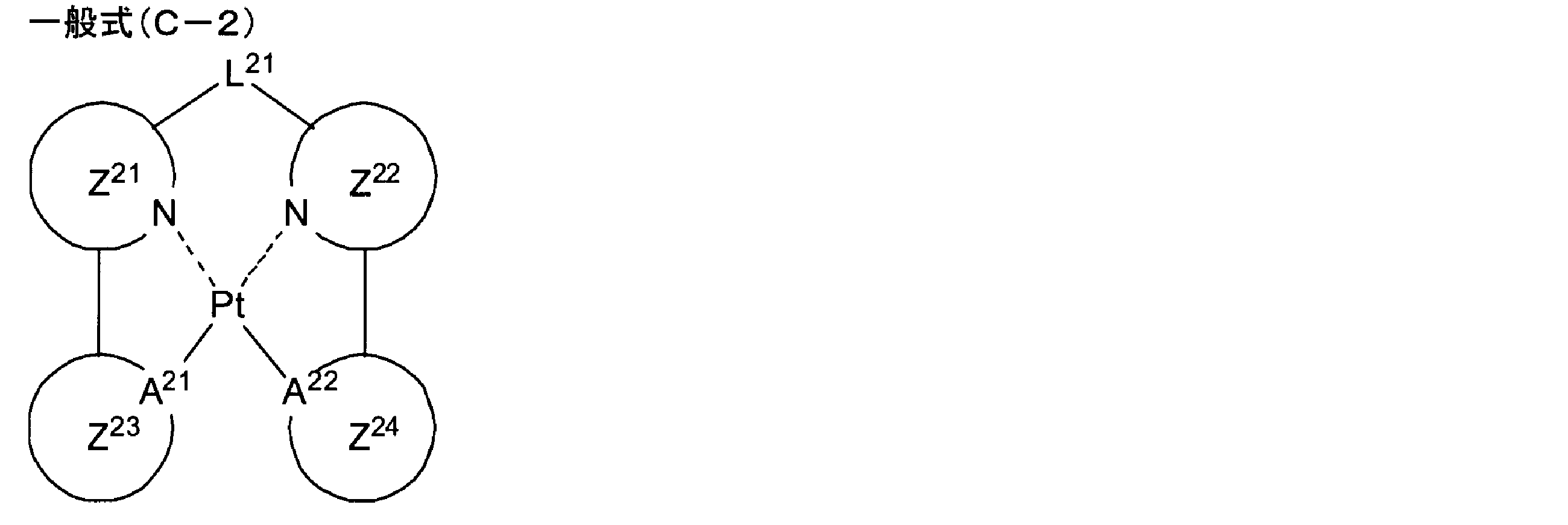
(式中、L21は単結合又は二価の連結基を表す。A21、A22はそれぞれ独立に炭素原子又は窒素原子を表す。Z21、Z22はそれぞれ独立に含窒素芳香族ヘテロ環を表す。Z23、Z24はそれぞれ独立にベンゼン環又は芳香族ヘテロ環を表す。)
(In the formula, L 21 represents a single bond or a divalent linking group. A 21 and A 22 each independently represents a carbon atom or a nitrogen atom. Z 21 and Z 22 each independently represent a nitrogen-containing aromatic heterocyclic ring. Z 23 and Z 24 each independently represents a benzene ring or an aromatic heterocycle.
一般式(C-2)について説明する。L21は、前記一般式(C-1)中のL1と同義であり、また好ましい範囲も同様である。
The general formula (C-2) will be described. L 21 has the same meaning as L 1 in formula (C-1), and the preferred range is also the same.
A21、A22はそれぞれ独立に炭素原子又は窒素原子を表す。A21、A22の内、少なくとも一方は炭素原子であることが好ましく、A21、A22が共に炭素原子であることが、錯体の安定性の観点及び錯体の発光量子収率の観点から好ましい。
A 21 and A 22 each independently represent a carbon atom or a nitrogen atom. Of A 21, A 22, Preferably, at least one is a carbon atom, it A 21, A 22 are both carbon atoms are preferred from the standpoint of emission quantum yield stability aspects and complexes of the complex .
Z21、Z22は、それぞれ独立に含窒素芳香族ヘテロ環を表す。Z21、Z22で表される含窒素芳香族ヘテロ環としては、ピリジン環、ピリミジン環、ピラジン環、トリアジン環、イミダゾール環、ピラゾール環、オキサゾール環、チアゾール環、トリアゾール環、オキサジアゾール環、チアジアゾール環などが挙げられる。錯体の安定性、発光波長制御及び発光量子収率の観点から、Z21、Z22で表される環として好ましくは、ピリジン環、ピラジン環、イミダゾール環、ピラゾール環であり、より好ましくはピリジン環、イミダゾール環、ピラゾール環であり、更に好ましくはピリジン環、ピラゾール環であり、特に好ましくはピリジン環である。
Z 21 and Z 22 each independently represent a nitrogen-containing aromatic heterocycle. Examples of the nitrogen-containing aromatic heterocycle represented by Z 21 and Z 22 include a pyridine ring, pyrimidine ring, pyrazine ring, triazine ring, imidazole ring, pyrazole ring, oxazole ring, thiazole ring, triazole ring, oxadiazole ring, Examples include thiadiazole rings. From the viewpoints of complex stability, emission wavelength control and emission quantum yield, the ring represented by Z 21 and Z 22 is preferably a pyridine ring, a pyrazine ring, an imidazole ring or a pyrazole ring, more preferably a pyridine ring. , An imidazole ring and a pyrazole ring, more preferably a pyridine ring and a pyrazole ring, and particularly preferably a pyridine ring.
Z23、Z24は、それぞれ独立にベンゼン環又は芳香族ヘテロ環を表す。Z23、Z24で表される含窒素芳香族ヘテロ環としては、ピリジン環、ピリミジン環、ピラジン環、ピリダジン環、トリアジン環、イミダゾール環、ピラゾール環、オキサゾール環、チアゾール環、トリアゾール環、オキサジアゾール環、チアジアゾール環、チオフェン環、フラン環などが挙げられる。錯体の安定性、発光波長制御及び発光量子収率の観点からZ23、Z24で表される環として好ましくは、ベンゼン環、ピリジン環、ピラジン環、イミダゾール環、ピラゾール環、チオフェン環であり、より好ましくはベンゼン環、ピリジン環、ピラゾール環であり、更に好ましくはベンゼン環、ピリジン環である。
Z 23 and Z 24 each independently represent a benzene ring or an aromatic heterocycle. Examples of the nitrogen-containing aromatic heterocycle represented by Z 23 and Z 24 include pyridine ring, pyrimidine ring, pyrazine ring, pyridazine ring, triazine ring, imidazole ring, pyrazole ring, oxazole ring, thiazole ring, triazole ring, oxadi Examples include an azole ring, a thiadiazole ring, a thiophene ring, and a furan ring. From the viewpoint of stability of the complex, emission wavelength control and emission quantum yield, the ring represented by Z 23 and Z 24 is preferably a benzene ring, a pyridine ring, a pyrazine ring, an imidazole ring, a pyrazole ring, or a thiophene ring. More preferred are a benzene ring, a pyridine ring and a pyrazole ring, and still more preferred are a benzene ring and a pyridine ring.
一般式(C-2)で表される白金(Pt)錯体のうち、より好ましい態様の一つは下記一般式(C-4)で表される白金(Pt)錯体である。
Of the platinum (Pt) complexes represented by the general formula (C-2), one of the more preferred embodiments is a platinum (Pt) complex represented by the following general formula (C-4).
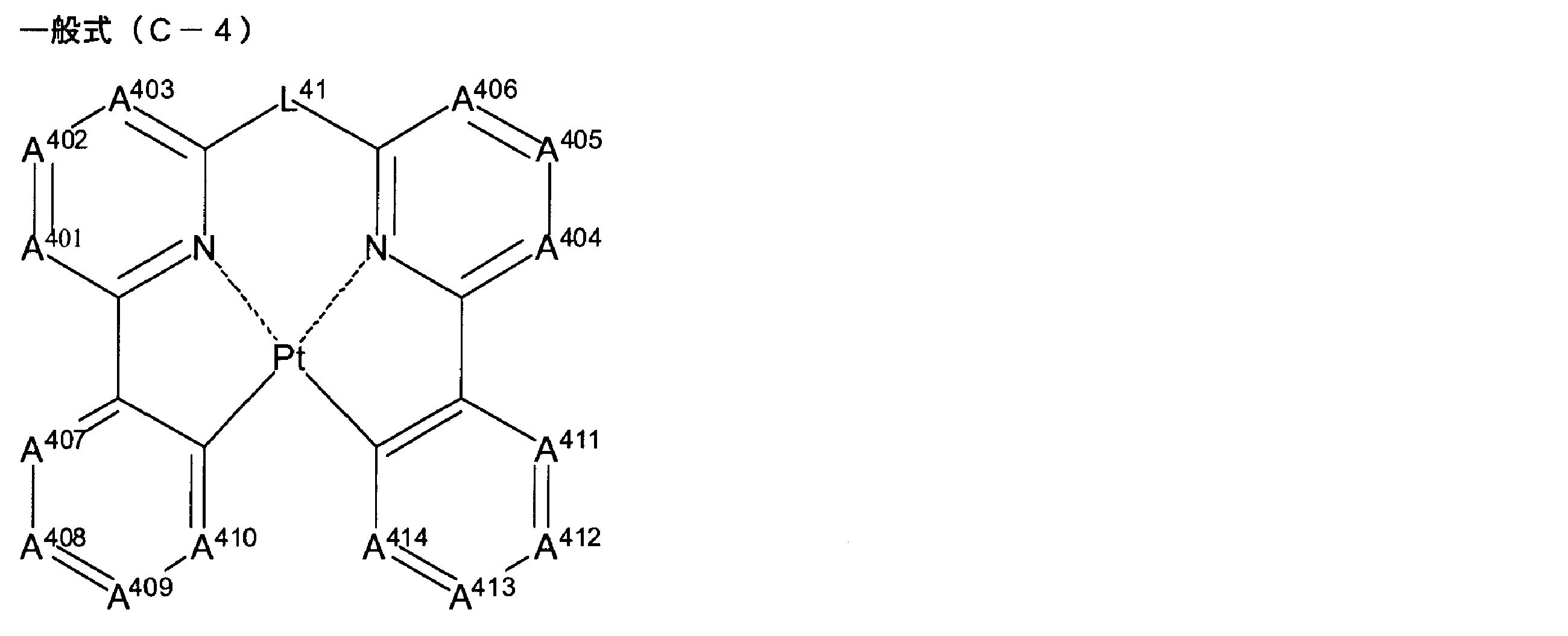
(一般式(C-4)中、A401~A414はそれぞれ独立にC-R又は窒素原子を表す。Rは水素原子又は置換基を表す。L41は単結合又は二価の連結基を表す。)
(In the general formula (C-4), A 401 to A 414 each independently represents C—R or a nitrogen atom. R represents a hydrogen atom or a substituent. L 41 represents a single bond or a divalent linking group. To express.)
一般式(C-4)について説明する。
A401~A414はそれぞれ独立にC-R又は窒素原子を表す。Rは水素原子又は置換基を表す。
Rで表される置換基としては、前記置換基群Aとして挙げたものが適用できる。
A401~A406として好ましくはC-Rであり、R同士が互いに連結して環を形成していても良い。A401~A406がC-Rである場合に、A402、A405のRとして好ましくは水素原子、アルキル基、アリール基、アミノ基、アルコキシ基、アリールオキシ基、フッ素原子、シアノ基であり、より好ましくは水素原子、アミノ基、アルコキシ基、アリールオキシ基、フッ素原子であり、特に好ましくは水素原子、フッ素原子である。A401、A403、A404、A406のRとして好ましくは水素原子、アルキル基、アリール基、アミノ基、アルコキシ基、アリールオキシ基、フッ素原子、シアノ基であり、より好ましくは水素原子、アミノ基、アルコキシ基、アリールオキシ基、フッ素原子であり、特に好ましく水素原子である。
L41は、前記一般式(C-1)中のL1と同義であり、また好ましい範囲も同様である。 The general formula (C-4) will be described.
A 401 to A 414 each independently represents C—R or a nitrogen atom. R represents a hydrogen atom or a substituent.
As the substituent represented by R, those exemplified as the substituent group A can be applied.
A 401 to A 406 are preferably C—R, and Rs may be connected to each other to form a ring. When A 401 to A 406 are C—R, R in A 402 and A 405 is preferably a hydrogen atom, an alkyl group, an aryl group, an amino group, an alkoxy group, an aryloxy group, a fluorine atom, or a cyano group. More preferred are a hydrogen atom, an amino group, an alkoxy group, an aryloxy group and a fluorine atom, and particularly preferred are a hydrogen atom and a fluorine atom. R in A 401 , A 403 , A 404 and A 406 is preferably a hydrogen atom, an alkyl group, an aryl group, an amino group, an alkoxy group, an aryloxy group, a fluorine atom or a cyano group, more preferably a hydrogen atom or amino Group, an alkoxy group, an aryloxy group and a fluorine atom, and particularly preferably a hydrogen atom.
L 41 has the same meaning as L 1 in formula (C-1), and the preferred range is also the same.
A407~A414としては、A407~A410とA411~A414のそれぞれにおいて、N(窒素原子)の数は、0~2が好ましく、0~1がより好ましい。発光波長を短波長側にシフトさせる場合、A408及びA412のいずれかが窒素原子であることが好ましく、A408とA412が共に窒素原子であることが更に好ましい。
As A 407 to A 414 , in each of A 407 to A 410 and A 411 to A 414 , the number of N (nitrogen atoms) is preferably 0 to 2, and more preferably 0 to 1. In the case of shifting the emission wavelength to the short wavelength side, either A 408 or A 412 is preferably a nitrogen atom, and more preferably both A 408 and A 412 are nitrogen atoms.
一般式(C-2)で表される白金(Pt)錯体のうち、より好ましい態様の一つは下記一般式(C-5)で表される白金(Pt)錯体である。
Of the platinum (Pt) complexes represented by the general formula (C-2), one of the more preferred embodiments is a platinum (Pt) complex represented by the following general formula (C-5).
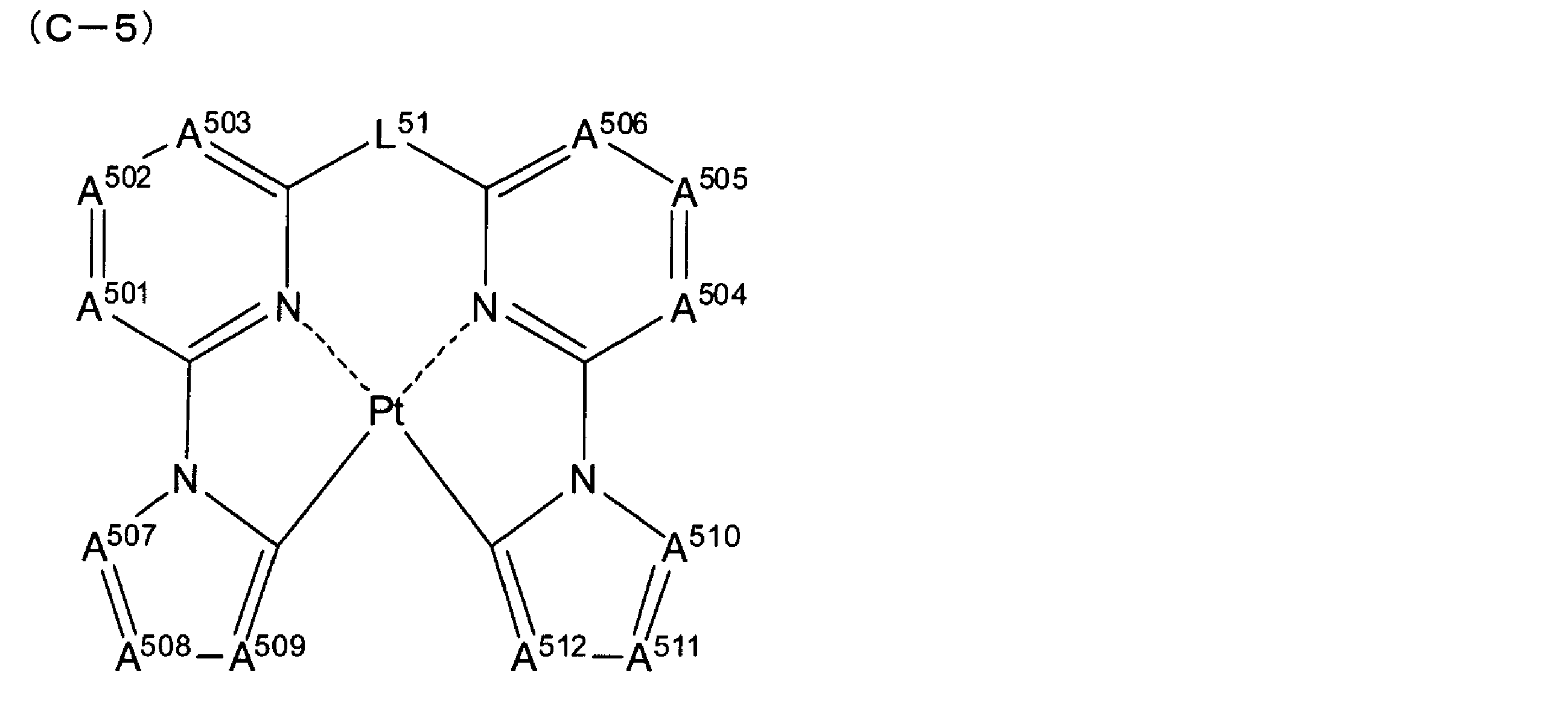
(一般式(C-5)中、A501~A512は、それぞれ独立に、C-R又は窒素原子を表す。Rは水素原子又は置換基を表す。L51は単結合又は二価の連結基を表す。)
(In the general formula (C-5), A 501 to A 512 each independently represents C—R or a nitrogen atom, R represents a hydrogen atom or a substituent, and L 51 represents a single bond or a divalent linkage. Represents a group.)
一般式(C-5)について説明する。A501~A506及びL51は、前記一般式(C-4)におけるA401~A406及びL41と同義であり、好ましい範囲も同様である。
The general formula (C-5) will be described. A 501 to A 506 and L 51 have the same meanings as A 401 to A 406 and L 41 in formula (C-4), and preferred ranges thereof are also the same.
A507、A508及びA509とA510、A511及びA512は、及びそれぞれ独立に、C-R又は窒素原子を表す。Rは水素原子又は置換基を表す。Rで表される置換基としては、前記置換基群Aとして挙げたものが適用できる。
A 507 , A 508 and A 509 and A 510 , A 511 and A 512 and each independently represent C—R or a nitrogen atom. R represents a hydrogen atom or a substituent. As the substituent represented by R, those exemplified as the substituent group A can be applied.
一般式(C-1)で表される白金(Pt)錯体のうち、より好ましい別の態様は下記一般式(C-6)で表される白金(Pt)錯体である。
Among the platinum (Pt) complexes represented by the general formula (C-1), another more preferable embodiment is a platinum (Pt) complex represented by the following general formula (C-6).
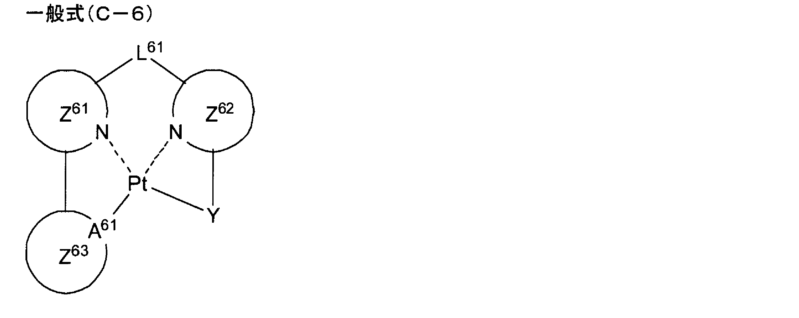
(式中、L61は単結合又は二価の連結基を表す。A61はそれぞれ独立に炭素原子又は窒素原子を表す。Z61、Z62はそれぞれ独立に含窒素芳香族ヘテロ環を表す。Z63はそれぞれ独立にベンゼン環又は芳香族ヘテロ環を表す。Yは白金(Pt)に結合するアニオン性の非環状配位子である。)
(In the formula, L 61 represents a single bond or a divalent linking group. A 61 independently represents a carbon atom or a nitrogen atom. Z 61 and Z 62 each independently represent a nitrogen-containing aromatic heterocycle. Z 63 independently represents a benzene ring or an aromatic heterocycle, and Y is an anionic acyclic ligand bonded to platinum (Pt).
一般式(C-6)について説明する。L61は、前記一般式(C-1)中のL1と同義であり、また好ましい範囲も同様である。
The general formula (C-6) will be described. L 61 has the same meaning as L 1 in formula (C-1), and the preferred range is also the same.
A61は炭素原子又は窒素原子を表す。錯体の安定性の観点及び錯体の発光量子収率の観点からA61は炭素原子であることが好ましい。
A 61 represents a carbon atom or a nitrogen atom. In view of the stability of the complex and the light emission quantum yield of the complex, A 61 is preferably a carbon atom.
Z61、Z62は、それぞれ前記一般式(C-2)におけるZ21、Z22と同義であり、また好ましい範囲も同様である。Z63は、前記一般式(C-2)におけるZ23と同義であり、また好ましい範囲も同様である。
Z 61 and Z 62 are synonymous with Z 21 and Z 22 in the general formula (C-2), respectively, and preferred ranges thereof are also the same. Z 63 has the same meaning as Z 23 in formula (C-2), and the preferred range is also the same.
Yは白金(Pt)に結合するアニオン性の非環状配位子である。非環状配位子とは白金(Pt)に結合する原子が配位子の状態で環を形成していないものである。Y中の白金(Pt)に結合する原子としては、炭素原子、窒素原子、酸素原子、硫黄原子が好ましく、窒素原子、酸素原子がより好ましく、酸素原子が最も好ましい。
炭素原子で白金(Pt)に結合するYとしてはビニル配位子が挙げられる。窒素原子で白金(Pt)に結合するYとしてはアミノ配位子、イミノ配位子が挙げられる。酸素原子で白金(Pt)に結合するYとしては、アルコキシ配位子、アリールオキシ配位子、ヘテロアリールオキシ配位子、アシルオキシ配位子、シリルオキシ配位子、カルボキシル配位子、リン酸配位子、スルホン酸配位子などが挙げられる。硫黄原子で白金(Pt)に結合するYとしては、アルキルメルカプト配位子、アリールメルカプト配位子、ヘテロアリールメルカプト配位子、チオカルボン酸配位子などが挙げられる。
Yで表される配位子は、置換基を有していてもよく、置換基としては前記置換基群Aとして挙げたものが適宜適用できる。また置換基同士が連結していても良い。 Y is an anionic acyclic ligand that binds to platinum (Pt). An acyclic ligand is one in which atoms bonded to platinum (Pt) do not form a ring in the state of a ligand. As an atom couple | bonded with platinum (Pt) in Y, a carbon atom, a nitrogen atom, an oxygen atom, and a sulfur atom are preferable, a nitrogen atom and an oxygen atom are more preferable, and an oxygen atom is the most preferable.
A vinyl ligand is mentioned as Y couple | bonded with platinum (Pt) by a carbon atom. Examples of Y bonded to platinum (Pt) with a nitrogen atom include an amino ligand and an imino ligand. Examples of Y bonded to platinum (Pt) with an oxygen atom include an alkoxy ligand, an aryloxy ligand, a heteroaryloxy ligand, an acyloxy ligand, a silyloxy ligand, a carboxyl ligand, and a phosphate group. Examples thereof include ligands and sulfonic acid ligands. Examples of Y bonded to platinum (Pt) with a sulfur atom include alkyl mercapto ligands, aryl mercapto ligands, heteroaryl mercapto ligands, and thiocarboxylic acid ligands.
The ligand represented by Y may have a substituent, and those listed as the substituent group A can be appropriately applied as the substituent. Moreover, substituents may be connected to each other.
Yで表される配位子として好ましくは酸素原子で白金(Pt)に結合する配位子であり、より好ましくはアシルオキシ配位子、アルキルオキシ配位子、アリールオキシ配位子、ヘテロアリールオキシ配位子、シリルオキシ配位子であり、更に好ましくはアシルオキシ配位子である。
The ligand represented by Y is preferably a ligand bonded to platinum (Pt) with an oxygen atom, and more preferably an acyloxy ligand, an alkyloxy ligand, an aryloxy ligand, a heteroaryloxy A ligand and a silyloxy ligand are preferable, and an acyloxy ligand is more preferable.
一般式(C-6)で表される白金(Pt)錯体のうち、より好ましい態様の一つは下記一般式(C-7)で表される白金(Pt)錯体である。
Of the platinum (Pt) complexes represented by the general formula (C-6), one of the more preferred embodiments is a platinum (Pt) complex represented by the following general formula (C-7).

(式中、A701~A710は、それぞれ独立に、C-R又は窒素原子を表す。Rは水素原子又は置換基を表す。L71は単結合又は二価の連結基を表す。Yは白金(Pt)に結合するアニオン性の非環状配位子である。)
(Wherein A 701 to A 710 each independently represents C—R or a nitrogen atom, R represents a hydrogen atom or a substituent, L 71 represents a single bond or a divalent linking group, Y represents (It is an anionic acyclic ligand that binds to platinum (Pt).)
一般式(C-7)について説明する。L71は、前記一般式(C-6)中のL61と同義であり、また好ましい範囲も同様である。A701~A710は一般式(C-4)におけるA401~A410と同義であり、また好ましい範囲も同様である。Yは一般式(C-6)におけるYと同義であり、また好ましい範囲も同様である。
The general formula (C-7) will be described. L 71 has the same meaning as L 61 in formula (C-6), and the preferred range is also the same. A 701 to A 710 have the same meanings as A 401 to A 410 in formula (C-4), and the preferred ranges are also the same. Y has the same meaning as Y in formula (C-6), and the preferred range is also the same.
一般式(C-1)で表される白金(Pt)錯体として具体的には、特開2005-310733号公報の〔0143〕~〔0152〕、〔0157〕~〔0158〕、〔0162〕~〔0168〕に記載の化合物、特開2006-256999号公報の〔0065〕~〔0083〕に記載の化合物、特開2006-93542号公報の〔0065〕~〔0090〕に記載の化合物、特開2007-73891号公報の〔0063〕~〔0071〕に記載の化合物、特開2007-324309号公報の〔0079〕~〔0083〕に記載の化合物、特開2006-93542号公報の〔0065〕~〔0090〕に記載の化合物、特開2007-96255号公報の〔0055〕~〔0071〕に記載の化合物、特開2006-313796号公報の〔0043〕~〔0046〕が挙げられ、その他以下に例示する白金(Pt)錯体が挙げられる。
Specific examples of the platinum (Pt) complex represented by the general formula (C-1) include [0143] to [0152], [0157] to [0158], and [0162] to JP-A-2005-310733. Compounds described in [0168], compounds described in JP-A-2006-256999, [0065]-[0083], compounds described in JP-A-2006-93542, [0065]-[0090], JP-A The compounds described in [0063] to [0071] of 2007-73491, the compounds described in [0079] to [0083] of JP 2007-324309, and [0065] to [0065] of JP 2006-93542 A Compounds described in [0090], compounds described in [0055] to [0071] of JP-A-2007-96255, JP-A-2006-31379 No. [0043] - [0046] can be mentioned publications, other include platinum (Pt) complex exemplified below.
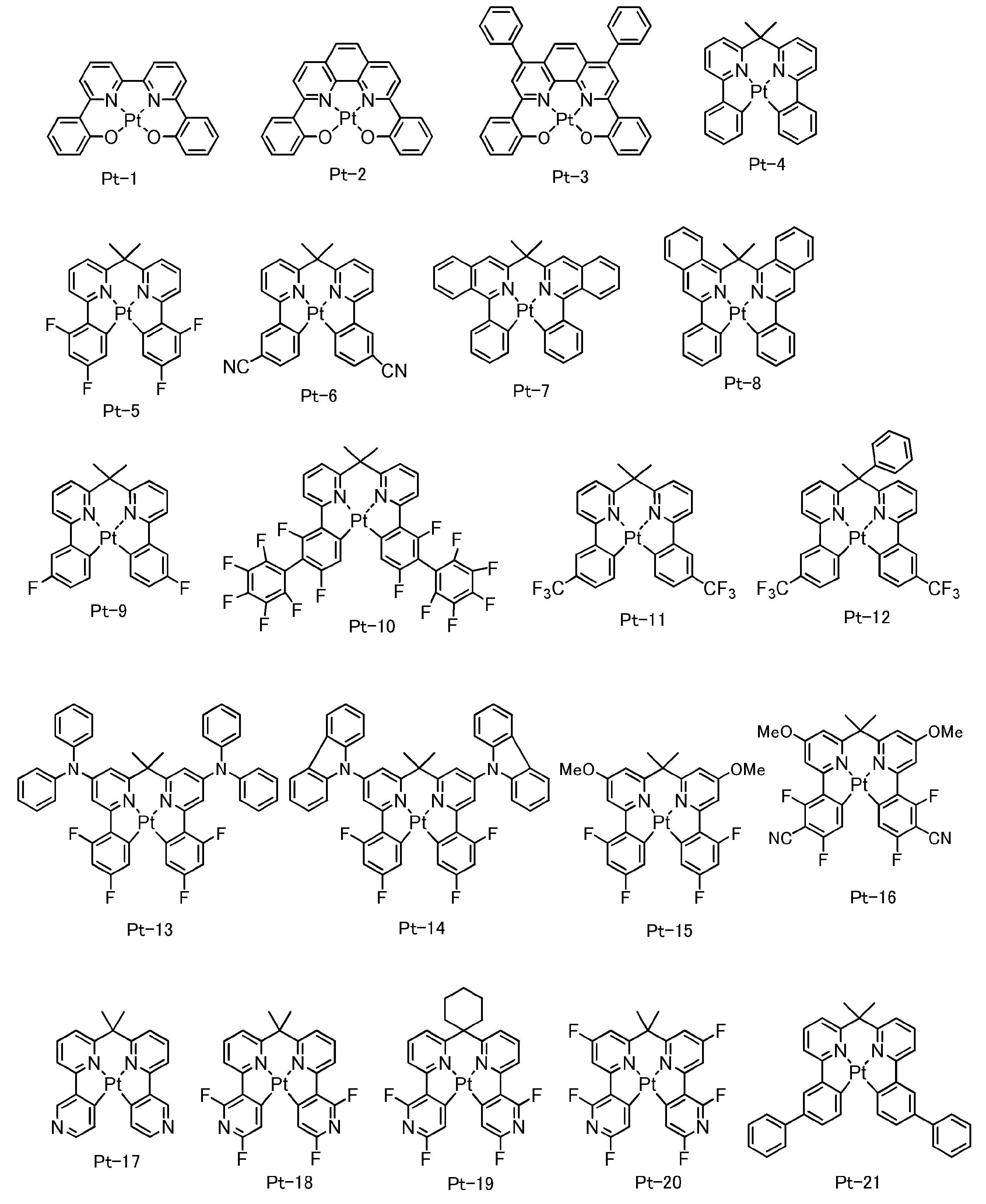
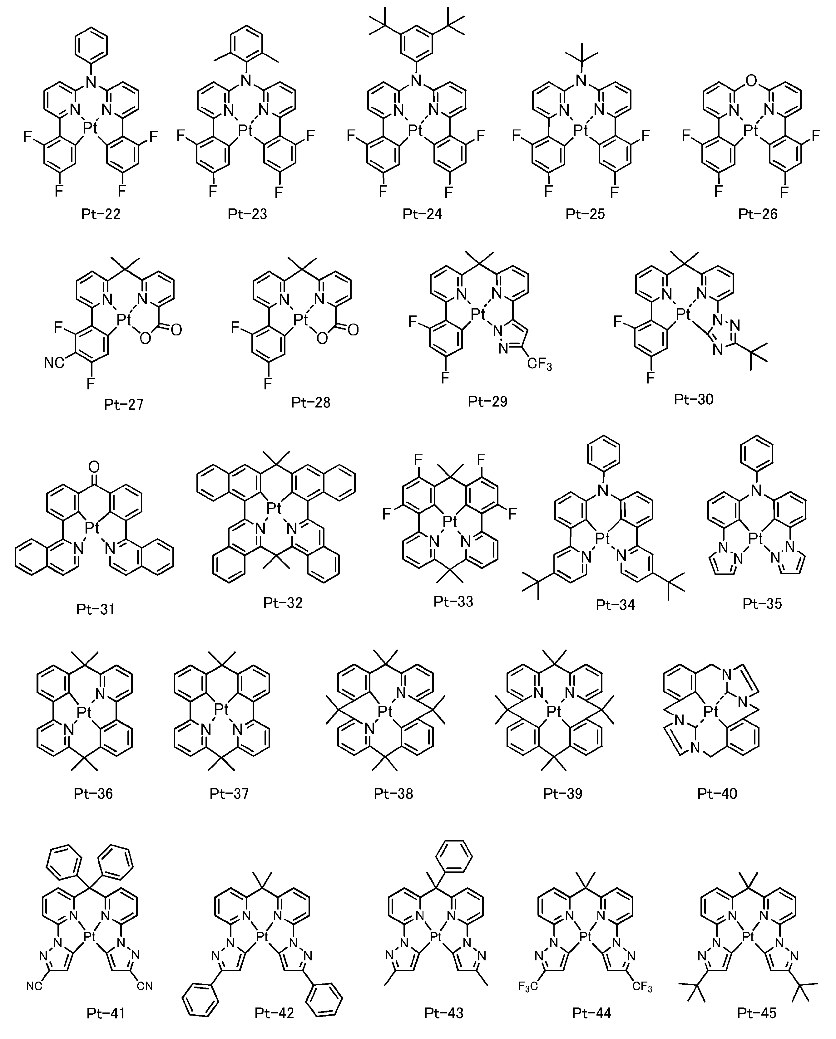
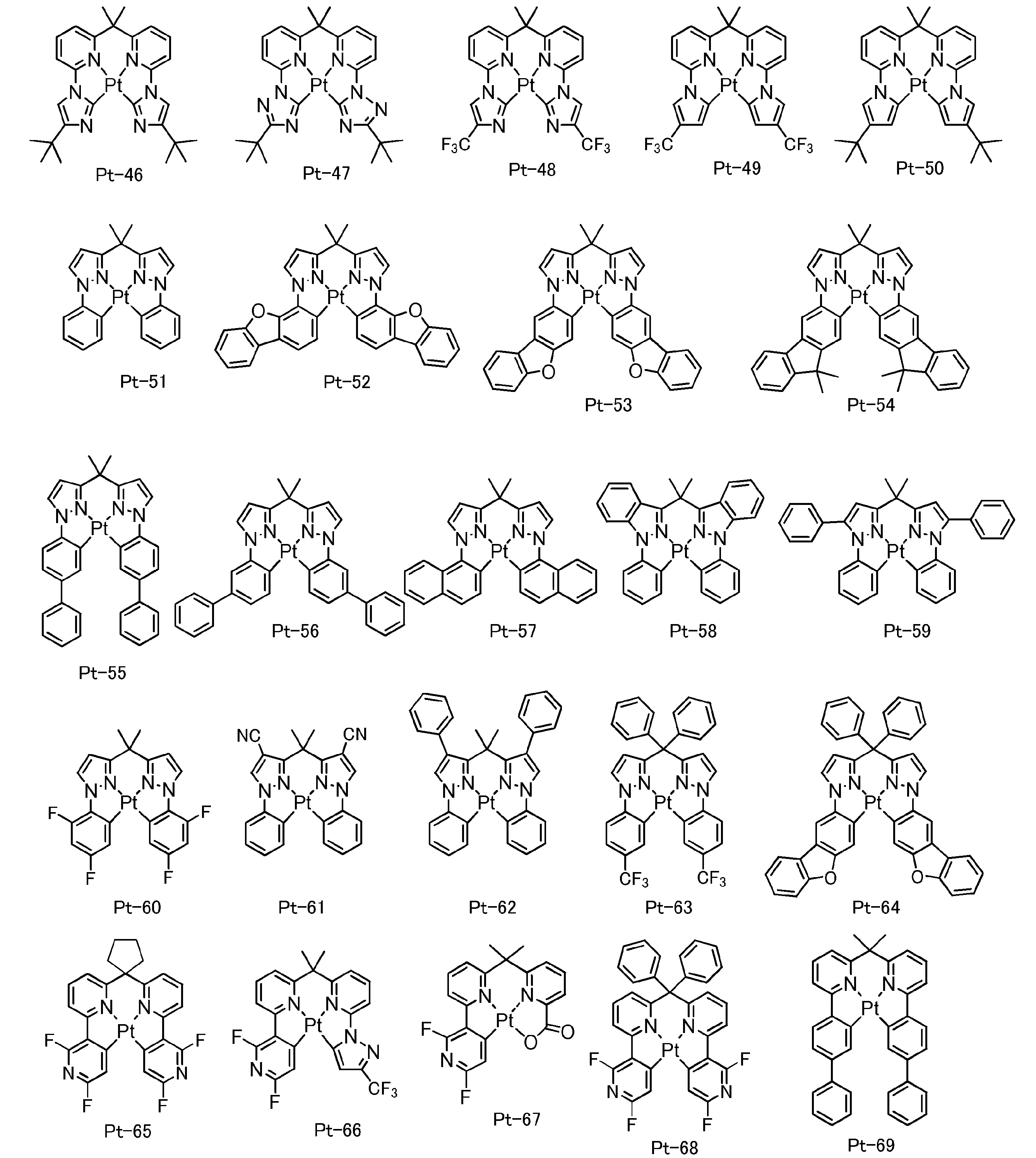
一般式(C-1)で表される白金(Pt)錯体化合物は、例えば、Journal of Organic Chemistry 53,786,(1988)、G.R.Newkome et al.)の、789頁、左段53行~右段7行に記載の方法、790頁、左段18行~38行に記載の方法、790頁、右段19行~30行に記載の方法及びその組み合わせ、Chemische Berichte 113,2749(1980)、H.Lexyほか)の、2752頁、26行~35行に記載の方法等、種々の手法で合成できる。
例えば、配位子、又はその解離体と金属化合物を溶媒(例えば、ハロゲン系溶媒、アルコール系溶媒、エーテル系溶媒、エステル系溶媒、ケトン系溶媒、ニトリル系溶媒、アミド系溶媒、スルホン系溶媒、スルホキサイド系溶媒、水などが挙げられる)の存在下、若しくは、溶媒非存在下、塩基の存在下(無機、有機の種々の塩基、例えば、ナトリウムメトキシド、t-ブトキシカリウム、トリエチルアミン、炭酸カリウムなどが挙げられる)、若しくは、塩基非存在下、室温以下、若しくは加熱し(通常の加熱以外にもマイクロウェーブで加熱する手法も有効である)得ることができる。 The platinum (Pt) complex compound represented by the general formula (C-1) is described in, for example, Journal of Organic Chemistry 53,786, (1988), G.A. R. Newkome et al. ), Page 789, method described in left column 53 toright column 7, line 790, method described in left column 18 to 38, method 790, method described in right column 19 to 30 and The combination, Chemische Berichte 113, 2749 (1980), H.C. Lexy et al.), Page 2752, lines 26 to 35, and the like.
For example, a ligand or a dissociated product thereof and a metal compound are mixed with a solvent (for example, a halogen solvent, an alcohol solvent, an ether solvent, an ester solvent, a ketone solvent, a nitrile solvent, an amide solvent, a sulfone solvent, In the presence of a sulfoxide solvent, water, etc., or in the absence of a solvent, in the presence of a base (inorganic and organic bases such as sodium methoxide, t-butoxypotassium, triethylamine, potassium carbonate, etc.) Or in the absence of a base, at room temperature or below, or by heating (in addition to normal heating, a method of heating with a microwave is also effective).
例えば、配位子、又はその解離体と金属化合物を溶媒(例えば、ハロゲン系溶媒、アルコール系溶媒、エーテル系溶媒、エステル系溶媒、ケトン系溶媒、ニトリル系溶媒、アミド系溶媒、スルホン系溶媒、スルホキサイド系溶媒、水などが挙げられる)の存在下、若しくは、溶媒非存在下、塩基の存在下(無機、有機の種々の塩基、例えば、ナトリウムメトキシド、t-ブトキシカリウム、トリエチルアミン、炭酸カリウムなどが挙げられる)、若しくは、塩基非存在下、室温以下、若しくは加熱し(通常の加熱以外にもマイクロウェーブで加熱する手法も有効である)得ることができる。 The platinum (Pt) complex compound represented by the general formula (C-1) is described in, for example, Journal of Organic Chemistry 53,786, (1988), G.A. R. Newkome et al. ), Page 789, method described in left column 53 to
For example, a ligand or a dissociated product thereof and a metal compound are mixed with a solvent (for example, a halogen solvent, an alcohol solvent, an ether solvent, an ester solvent, a ketone solvent, a nitrile solvent, an amide solvent, a sulfone solvent, In the presence of a sulfoxide solvent, water, etc., or in the absence of a solvent, in the presence of a base (inorganic and organic bases such as sodium methoxide, t-butoxypotassium, triethylamine, potassium carbonate, etc.) Or in the absence of a base, at room temperature or below, or by heating (in addition to normal heating, a method of heating with a microwave is also effective).
本発明の発光層における一般式(C-1)で表される化合物の含有量は発光層中1~30質量%であることが好ましく、3~25質量%であることがより好ましく、5~20質量%であることが更に好ましい。
The content of the compound represented by formula (C-1) in the light emitting layer of the present invention is preferably 1 to 30% by mass, more preferably 3 to 25% by mass in the light emitting layer. More preferably, it is 20 mass%.
前記蛍光発光材料の種類は特に限定されるものではないが、例えば、ベンゾオキサゾール、ベンゾイミダゾール、ベンゾチアゾール、スチリルベンゼン、ポリフェニル、ジフェニルブタジエン、テトラフェニルブタジエン、ナフタルイミド、クマリン、ピラン、ペリノン、オキサジアゾール、アルダジン、ピラリジン、シクロペンタジエン、ビススチリルアントラセン、キナクリドン、ピロロピリジン、チアジアゾロピリジン、シクロペンタジエン、スチリルアミン、縮合多環芳香族化合物(アントラセン、フェナントロリン、ピレン、フルオランテン、ペリレン、ルブレン、又はペンタセンなど)、8-キノリノールの金属錯体、ピロメテン錯体や希土類錯体に代表される各種金属錯体、ポリチオフェン、ポリフェニレン、ポリフェニレンビニレン等のポリマー化合物、有機シラン、及びこれらの誘導体などを挙げることができる。
The type of the fluorescent material is not particularly limited. For example, benzoxazole, benzimidazole, benzothiazole, styrylbenzene, polyphenyl, diphenylbutadiene, tetraphenylbutadiene, naphthalimide, coumarin, pyran, perinone, oxa Diazole, aldazine, pyralidine, cyclopentadiene, bisstyrylanthracene, quinacridone, pyrrolopyridine, thiadiazolopyridine, cyclopentadiene, styrylamine, condensed polycyclic aromatic compounds (anthracene, phenanthroline, pyrene, fluoranthene, perylene, rubrene, or Pentacene, etc.), metal complexes of 8-quinolinol, various metal complexes represented by pyromethene complexes and rare earth complexes, polythiophene, polyphenylene, polyphenyle Polymeric compounds such as vinylene, organic silane, and may be derivatives of these.
発光層の厚さは、特に限定されるものではないが、通常、2nm~500nmであるのが好ましく、中でも、外部量子効率の観点で、5nm~200nmであるのがより好ましく、10nm~100nmであるのが更に好ましい。
The thickness of the light emitting layer is not particularly limited, but is usually preferably 2 nm to 500 nm, and more preferably 5 nm to 200 nm, and more preferably 10 nm to 100 nm, from the viewpoint of external quantum efficiency. More preferably.
本発明の有機電界発光素子における発光層は、発光材料のみで構成されていてもよく、ホスト材料と発光材料の混合層とした構成でもよい。発光材料の種類は一種であっても二種以上であっても良い。ホスト材料は電荷輸送材料であることが好ましい。ホスト材料は一種であっても二種以上であってもよく、例えば、電子輸送性のホスト材料と正孔輸送性のホスト材料を混合した構成が挙げられる。更に、発光層中に電荷輸送性を有さず、発光しない材料を含んでいてもよい。
また、発光層は一層であっても二層以上の多層であってもよく、それぞれの層に同じ発光材料やホスト材料を含んでもよいし、層毎に異なる材料を含んでもよい。発光層が複数の場合、それぞれの発光層が異なる発光色で発光してもよい。 The light emitting layer in the organic electroluminescent element of the present invention may be composed only of a light emitting material, or may be a mixed layer of a host material and a light emitting material. The kind of the light emitting material may be one kind or two or more kinds. The host material is preferably a charge transport material. The host material may be one kind or two or more kinds, and examples thereof include a configuration in which an electron transporting host material and a hole transporting host material are mixed. Furthermore, the light emitting layer may contain a material that does not have charge transporting properties and does not emit light.
Further, the light emitting layer may be a single layer or a multilayer of two or more layers, and each layer may contain the same light emitting material or host material, or each layer may contain a different material. When there are a plurality of light emitting layers, each of the light emitting layers may emit light with different emission colors.
(ホスト材料)
ホスト材料とは、発光層において主に電荷の注入、輸送を担う化合物であり、また、それ自体は実質的に発光しない化合物のことである。ここで「実質的に発光しない」とは、該実質的に発光しない化合物からの発光量が好ましくは素子全体での全発光量の5%以下であり、より好ましくは3%以下であり、更に好ましくは1%以下であることを言う。
ホスト材料としては、一般式(1)で表される化合物を用いることができる。 (Host material)
The host material is a compound mainly responsible for charge injection and transport in the light emitting layer, and itself is a compound that does not substantially emit light. Here, “substantially does not emit light” means that the amount of light emitted from the compound that does not substantially emit light is preferably 5% or less, more preferably 3% or less of the total amount of light emitted from the entire device. Preferably it says 1% or less.
As the host material, a compound represented by the general formula (1) can be used.
その他の本発明有機電界発光素子に用いることのできるホスト材料としては、例えば、以下の化合物を挙げることができる。
ピロール、インドール、カルバゾール、アザインドール、アザカルバゾール、トリアゾール、オキサゾール、オキサジアゾール、ピラゾール、イミダゾール、チオフェン、ベンゾチオフェン、ジベンゾチオフェン、フラン、ベンゾフラン、ジベンゾフラン、ポリアリールアルカン、ピラゾリン、ピラゾロン、フェニレンジアミン、アリールアミン、アミノ置換カルコン、スチリルアントラセン、フルオレノン、ヒドラゾン、スチルベン、シラザン、芳香族第三級アミン化合物、スチリルアミン化合物、ポルフィリン系化合物、縮環芳香族炭化水素化合物(フルオレン、ナフタレン、フェナントレン、トリフェニレン等)、ポリシラン系化合物、ポリ(N-ビニルカルバゾール)、アニリン系共重合体、チオフェンオリゴマー、ポリチオフェン等の導電性高分子オリゴマー、有機シラン、カーボン膜、ピリジン、ピリミジン、トリアジン、イミダゾール、ピラゾール、トリアゾ-ル、オキサゾ-ル、オキサジアゾ-ル、フルオレノン、アントラキノジメタン、アントロン、ジフェニルキノン、チオピランジオキシド、カルボジイミド、フルオレニリデンメタン、ジスチリルピラジン、フッ素置換芳香族化合物、ナフタレンペリレン等の複素環テトラカルボン酸無水物、フタロシアニン、8-キノリノ-ル誘導体の金属錯体やメタルフタロシアニン、ベンゾオキサゾ-ルやベンゾチアゾ-ルを配位子とする金属錯体に代表される各種金属錯体及びそれらの誘導体(置換基や縮環を有していてもよい)等を挙げることができる。
これらのうち、カルバゾール、ジベンゾチオフェン、ジベンゾフラン、アリールアミン、縮環芳香族炭化水素化合物、金属錯体が特に好ましい。 Examples of other host materials that can be used in the organic electroluminescence device of the present invention include the following compounds.
Pyrrole, indole, carbazole, azaindole, azacarbazole, triazole, oxazole, oxadiazole, pyrazole, imidazole, thiophene, benzothiophene, dibenzothiophene, furan, benzofuran, dibenzofuran, polyarylalkane, pyrazoline, pyrazolone, phenylenediamine, aryl Amines, amino-substituted chalcones, styrylanthracenes, fluorenones, hydrazones, stilbenes, silazanes, aromatic tertiary amine compounds, styrylamine compounds, porphyrin compounds, condensed aromatic hydrocarbon compounds (fluorene, naphthalene, phenanthrene, triphenylene, etc.) , Polysilane compound, poly (N-vinylcarbazole), aniline copolymer, thiophene oligomer, polythiophene Conductive polymer oligomer, organic silane, carbon film, pyridine, pyrimidine, triazine, imidazole, pyrazole, triazole, oxazole, oxadiazol, fluorenone, anthraquinodimethane, anthrone, diphenylquinone, thiopyrandi Oxides, carbodiimides, fluorenylidenemethane, distyrylpyrazine, fluorine-substituted aromatic compounds, heterocyclic tetracarboxylic anhydrides such as naphthaleneperylene, metal complexes of phthalocyanines and 8-quinolinol derivatives, metal phthalocyanines, benzoxazoles, Examples thereof include various metal complexes represented by metal complexes having benzothiazol as a ligand and derivatives thereof (which may have a substituent or a condensed ring).
Of these, carbazole, dibenzothiophene, dibenzofuran, arylamine, fused aromatic hydrocarbon compounds, and metal complexes are particularly preferable.
本発明の有機電界発光素子における発光層において、併用することができるホスト材料としては、正孔輸送性ホスト材料であっても、電子輸送性ホスト材料であってもよい。
The host material that can be used in combination in the light emitting layer of the organic electroluminescent device of the present invention may be a hole transporting host material or an electron transporting host material.
発光層において、前記ホスト材料の膜状態での三重項最低励起エネルギー(T1エネルギー)が、前記燐光発光材料のT1エネルギーより高いことが色純度、発光効率、駆動耐久性の点で好ましい。ホスト材料のT1が燐光発光材料のT1より0.1eV以上大きいことが好ましく、0.2eV以上大きいことがより好ましく、0.3eV以上大きいことが更に好ましい。
ホスト材料の膜状態でのT1が燐光発光材料のT1より小さいと発光を消光してしまうためホスト材料には燐光発光材料より大きなT1が求められる。また、ホスト材料のT1が燐光発光材料より大きい場合でも、両者のT1差が小さい場合には一部、燐光発光材料からホスト材料への逆エネルギー移動が起こるため、効率低下や耐久性低下の原因となる。従って、T1が十分に大きく、化学的安定性及びキャリア注入・輸送性の高いホスト材料が求められている。 In the light emitting layer, the triplet lowest excitation energy (T 1 energy) in the film state of the host material is preferably higher than the T 1 energy of the phosphorescent light emitting material in terms of color purity, light emission efficiency, and driving durability. It is preferable T 1 is greater 0.1eV higher than the T 1 of the phosphorescent material of the host material, more preferably at least 0.2eV higher, and further preferably more than 0.3eV large.
T 1 of the a film state of the host material is a large T 1 is obtained from the phosphorescent material to the host material for thereby quench T 1 is less than the light emission of the phosphorescent material. Even if the T 1 of the host material is larger than the phosphorescent light emitting material, if the difference in T 1 between the two is small, the reverse energy transfer from the phosphorescent light emitting material to the host material occurs in part, resulting in a decrease in efficiency and durability. Cause. Therefore, there is a demand for a host material having a sufficiently large T 1 and high chemical stability and carrier injection / transport properties.
また、本発明有機電界発光素子における発光層におけるホスト化合物の含有量は、特に限定されるものではないが、発光効率、駆動電圧の観点から、発光層を形成する全化合物質量に対して15質量%以上95質量%以下であることが好ましい。発光層に、一般式(1)で表される化合物を含む複数種類のホスト化合物を含む場合、一般式(1)で表される化合物は全ホスト化合物中50質量%以上99質量%以下であることが好ましい。
In addition, the content of the host compound in the light emitting layer in the organic electroluminescent device of the present invention is not particularly limited, but is 15 mass with respect to the total compound mass forming the light emitting layer from the viewpoint of light emission efficiency and driving voltage. % Or more and 95% by mass or less is preferable. When the light emitting layer contains a plurality of types of host compounds including the compound represented by the general formula (1), the compound represented by the general formula (1) is 50% by mass or more and 99% by mass or less in all the host compounds. It is preferable.
(その他の層)
本発明の有機電界発光素子は、前記発光層以外のその他の層を有していてもよい。
前記有機層が有していてもよい前記発光層以外のその他の有機層として、正孔注入層、正孔輸送層、ブロック層(正孔ブロック層、励起子ブロック層、電子ブロック層など)、電子輸送層などが挙げられる。前記具体的な層構成として、下記が挙げられるが本発明はこれらの構成に限定されるものではない。
・陽極/正孔輸送層/発光層/電子輸送層/陰極、
・陽極/正孔輸送層/発光層/ブロック層/電子輸送層/陰極、
・陽極/正孔輸送層/発光層/ブロック層/電子輸送層/電子注入層/陰極、
・陽極/正孔注入層/正孔輸送層/発光層/ブロック層/電子輸送層/陰極、
・陽極/正孔注入層/正孔輸送層/発光層/電子輸送層/電子注入層/陰極、
・陽極/正孔注入層/正孔輸送層/発光層/ブロック層/電子輸送層/電子注入層/陰極、
・陽極/正孔注入層/正孔輸送層/ブロック層/発光層/ブロック層/電子輸送層/電子注入層/陰極。
本発明の有機電界発光素子は、(A)前記陽極と前記発光層との間に好ましく配置される有機層を少なくとも一層含むことが好ましい。前記(A)前記陽極と前記発光層との間に好ましく配置される有機層としては、陽極側から正孔注入層、正孔輸送層、電子ブロック層を挙げることができる。
本発明の有機電界発光素子は、(B)前記陰極と前記発光層との間に好ましく配置される有機層少なくとも一層含むことが好ましい。前記(B)前記陰極と前記発光層との間に好ましく配置される有機層としては、陰極側から電子注入層、電子輸送層、正孔ブロック層を挙げることができる。
具体的には、本発明の有機電界発光素子の好ましい態様の一例は、図1に記載される態様であり、前記有機層として、陽極側3から正孔注入層4、正孔輸送層5、発光層6、正孔ブロック層7及び電子輸送層8がこの順に積層されている態様である。
以下、これら本発明の有機電界発光素子が有していてもよい前記発光層以外のその他の層について、説明する。 (Other layers)
The organic electroluminescent element of the present invention may have other layers other than the light emitting layer.
Other organic layers other than the light emitting layer that the organic layer may have include a hole injection layer, a hole transport layer, a block layer (hole block layer, exciton block layer, electron block layer, etc.), Examples thereof include an electron transport layer. Examples of the specific layer configuration include the following, but the present invention is not limited to these configurations.
Anode / hole transport layer / light emitting layer / electron transport layer / cathode,
Anode / hole transport layer / light emitting layer / block layer / electron transport layer / cathode,
Anode / hole transport layer / light emitting layer / block layer / electron transport layer / electron injection layer / cathode,
Anode / hole injection layer / hole transport layer / light emitting layer / block layer / electron transport layer / cathode,
Anode / hole injection layer / hole transport layer / light emitting layer / electron transport layer / electron injection layer / cathode,
Anode / hole injection layer / hole transport layer / light emitting layer / block layer / electron transport layer / electron injection layer / cathode,
Anode / hole injection layer / hole transport layer / block layer / light emitting layer / block layer / electron transport layer / electron injection layer / cathode.
The organic electroluminescent element of the present invention preferably includes (A) at least one organic layer preferably disposed between the anode and the light emitting layer. Examples of the organic layer (A) preferably disposed between the anode and the light emitting layer include a hole injection layer, a hole transport layer, and an electron block layer from the anode side.
The organic electroluminescent element of the present invention preferably includes (B) at least one organic layer preferably disposed between the cathode and the light emitting layer. Examples of the organic layer (B) preferably disposed between the cathode and the light emitting layer include an electron injection layer, an electron transport layer, and a hole blocking layer from the cathode side.
Specifically, an example of a preferred embodiment of the organic electroluminescent element of the present invention is the embodiment described in FIG. 1, and as the organic layer, ahole injection layer 4, a hole transport layer 5, In this embodiment, the light emitting layer 6, the hole blocking layer 7, and the electron transport layer 8 are laminated in this order.
Hereinafter, other layers other than the light emitting layer which may be included in the organic electroluminescent element of the present invention will be described.
本発明の有機電界発光素子は、前記発光層以外のその他の層を有していてもよい。
前記有機層が有していてもよい前記発光層以外のその他の有機層として、正孔注入層、正孔輸送層、ブロック層(正孔ブロック層、励起子ブロック層、電子ブロック層など)、電子輸送層などが挙げられる。前記具体的な層構成として、下記が挙げられるが本発明はこれらの構成に限定されるものではない。
・陽極/正孔輸送層/発光層/電子輸送層/陰極、
・陽極/正孔輸送層/発光層/ブロック層/電子輸送層/陰極、
・陽極/正孔輸送層/発光層/ブロック層/電子輸送層/電子注入層/陰極、
・陽極/正孔注入層/正孔輸送層/発光層/ブロック層/電子輸送層/陰極、
・陽極/正孔注入層/正孔輸送層/発光層/電子輸送層/電子注入層/陰極、
・陽極/正孔注入層/正孔輸送層/発光層/ブロック層/電子輸送層/電子注入層/陰極、
・陽極/正孔注入層/正孔輸送層/ブロック層/発光層/ブロック層/電子輸送層/電子注入層/陰極。
本発明の有機電界発光素子は、(A)前記陽極と前記発光層との間に好ましく配置される有機層を少なくとも一層含むことが好ましい。前記(A)前記陽極と前記発光層との間に好ましく配置される有機層としては、陽極側から正孔注入層、正孔輸送層、電子ブロック層を挙げることができる。
本発明の有機電界発光素子は、(B)前記陰極と前記発光層との間に好ましく配置される有機層少なくとも一層含むことが好ましい。前記(B)前記陰極と前記発光層との間に好ましく配置される有機層としては、陰極側から電子注入層、電子輸送層、正孔ブロック層を挙げることができる。
具体的には、本発明の有機電界発光素子の好ましい態様の一例は、図1に記載される態様であり、前記有機層として、陽極側3から正孔注入層4、正孔輸送層5、発光層6、正孔ブロック層7及び電子輸送層8がこの順に積層されている態様である。
以下、これら本発明の有機電界発光素子が有していてもよい前記発光層以外のその他の層について、説明する。 (Other layers)
The organic electroluminescent element of the present invention may have other layers other than the light emitting layer.
Other organic layers other than the light emitting layer that the organic layer may have include a hole injection layer, a hole transport layer, a block layer (hole block layer, exciton block layer, electron block layer, etc.), Examples thereof include an electron transport layer. Examples of the specific layer configuration include the following, but the present invention is not limited to these configurations.
Anode / hole transport layer / light emitting layer / electron transport layer / cathode,
Anode / hole transport layer / light emitting layer / block layer / electron transport layer / cathode,
Anode / hole transport layer / light emitting layer / block layer / electron transport layer / electron injection layer / cathode,
Anode / hole injection layer / hole transport layer / light emitting layer / block layer / electron transport layer / cathode,
Anode / hole injection layer / hole transport layer / light emitting layer / electron transport layer / electron injection layer / cathode,
Anode / hole injection layer / hole transport layer / light emitting layer / block layer / electron transport layer / electron injection layer / cathode,
Anode / hole injection layer / hole transport layer / block layer / light emitting layer / block layer / electron transport layer / electron injection layer / cathode.
The organic electroluminescent element of the present invention preferably includes (A) at least one organic layer preferably disposed between the anode and the light emitting layer. Examples of the organic layer (A) preferably disposed between the anode and the light emitting layer include a hole injection layer, a hole transport layer, and an electron block layer from the anode side.
The organic electroluminescent element of the present invention preferably includes (B) at least one organic layer preferably disposed between the cathode and the light emitting layer. Examples of the organic layer (B) preferably disposed between the cathode and the light emitting layer include an electron injection layer, an electron transport layer, and a hole blocking layer from the cathode side.
Specifically, an example of a preferred embodiment of the organic electroluminescent element of the present invention is the embodiment described in FIG. 1, and as the organic layer, a
Hereinafter, other layers other than the light emitting layer which may be included in the organic electroluminescent element of the present invention will be described.
(A)陽極と前記発光層との間に好ましく配置される有機層
まず、(A)前記陽極と前記発光層との間に好ましく配置される有機層について説明する。 (A) Organic layer preferably disposed between the anode and the light emitting layer First, (A) the organic layer preferably disposed between the anode and the light emitting layer will be described.
まず、(A)前記陽極と前記発光層との間に好ましく配置される有機層について説明する。 (A) Organic layer preferably disposed between the anode and the light emitting layer First, (A) the organic layer preferably disposed between the anode and the light emitting layer will be described.
(A-1)正孔注入層、正孔輸送層
正孔注入層、正孔輸送層は、陽極又は陽極側から正孔を受け取り陰極側に輸送する機能を有する層である。
正孔注入層、正孔輸送層については、特開2008-270736号公報の段落番号〔0165〕~〔0167〕に記載の事項を本発明に適用することができる。その中でも、正孔注入層、正孔輸送層に好ましく用いられる材料について説明する。 (A-1) Hole injection layer, hole transport layer The hole injection layer and the hole transport layer are layers having a function of receiving holes from the anode or the anode side and transporting them to the cathode side.
For the hole injection layer and the hole transport layer, the matters described in paragraph numbers [0165] to [0167] of JP-A-2008-270736 can be applied to the present invention. Among these, the material preferably used for the hole injection layer and the hole transport layer will be described.
本発明の有機電界発光素子は、下記の化合物を前記発光層と前記陽極との間の有機層に含有することが好ましく、正孔注入層に含有することがより好ましい。
具体的には、以下の構造の化合物が好ましい。


The organic electroluminescent element of the present invention preferably contains the following compound in the organic layer between the light emitting layer and the anode, and more preferably in the hole injection layer.
Specifically, a compound having the following structure is preferable.
具体的には、以下の構造の化合物が好ましい。
Specifically, a compound having the following structure is preferable.
本発明の有機電界発光素子は、少なくとも一種の下記一般式(M-1)で表される化合物を前記発光層と前記陽極との間の有機層に含有することが好ましく、正孔輸送層に含有することがより好ましい。
The organic electroluminescent element of the present invention preferably contains at least one compound represented by the following general formula (M-1) in the organic layer between the light emitting layer and the anode, and the hole transport layer contains It is more preferable to contain.
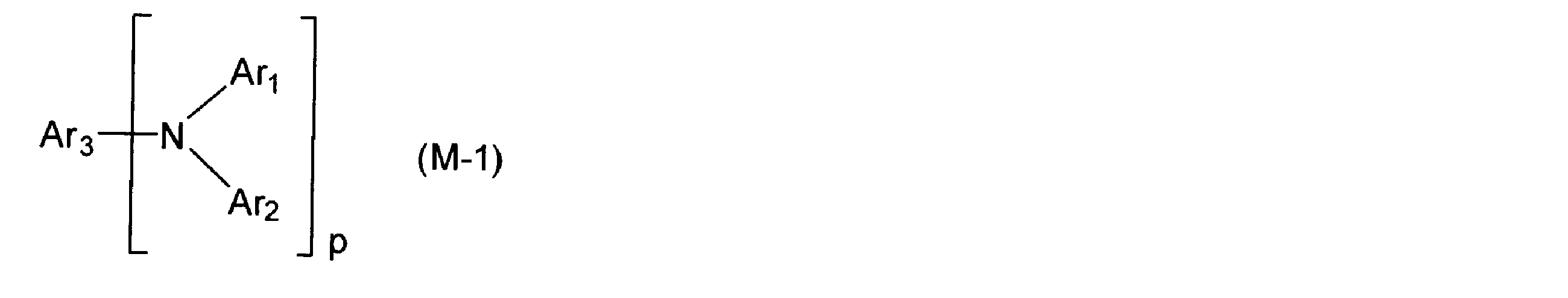
一般式(M-1)中、Ar1及びAr2はそれぞれ独立してアルキル、アリール、ヘテロアリール、アリールアミノ、アルキルアミノ、モルホリノ、チオモルホリノ、N、O、及びSから選択される1以上のヘテロ原子を含有する5若しくは6員へテロシクロアルキル又はシクロアルキルを表し、更に置換基Zを有していてもよい。またAr1及びAr2は、単結合、アルキレン、若しくはアルケニレン(縮合環の有無を問わない)により互いに結合して、縮合5~9員環を形成してもよい。
Ar3はアルキル、アリール、ヘテロアリール、アリールアミノを表し、更に置換基Zを有していてもよい。
Zはそれぞれ独立に、ハロゲン原子、-R"、-OR"、-N(R")2、-SR"、-C(O)R"、-C(O)OR"、-C(O)N(R")2、-CN、-NO2、-SO2、-SOR"、-SO2R"、又は-SO3R"を表し、R"はそれぞれ独立に、水素原子、アルキル基、ペルハロアルキル基、アルケニル基、アルキニル基、ヘテロアルキル基、アリール基又はヘテロアリール基を表す。
pは1~4の整数であり、pが2以上のときAr1及びAr2はそれぞれ同一でも異なっていてもよい。 In general formula (M-1), Ar 1 and Ar 2 are each independently one or more selected from alkyl, aryl, heteroaryl, arylamino, alkylamino, morpholino, thiomorpholino, N, O, and S It represents a 5- or 6-membered heterocycloalkyl or cycloalkyl containing a hetero atom, and may further have a substituent Z. Ar 1 and Ar 2 may be bonded to each other by a single bond, alkylene, or alkenylene (with or without a condensed ring) to form a condensed 5- to 9-membered ring.
Ar 3 represents alkyl, aryl, heteroaryl, or arylamino, and may further have a substituent Z.
Z is independently a halogen atom, -R ", -OR", -N (R ") 2 , -SR", -C (O) R ", -C (O) OR", -C (O) N (R ") 2, -CN , -NO 2, -SO 2, -SOR", - SO 2 R ", or -SO 3 R" represents, R "are each independently a hydrogen atom, an alkyl group, A perhaloalkyl group, an alkenyl group, an alkynyl group, a heteroalkyl group, an aryl group or a heteroaryl group is represented.
p is an integer of 1 to 4, and when p is 2 or more, Ar 1 and Ar 2 may be the same or different.
Ar3はアルキル、アリール、ヘテロアリール、アリールアミノを表し、更に置換基Zを有していてもよい。
Zはそれぞれ独立に、ハロゲン原子、-R"、-OR"、-N(R")2、-SR"、-C(O)R"、-C(O)OR"、-C(O)N(R")2、-CN、-NO2、-SO2、-SOR"、-SO2R"、又は-SO3R"を表し、R"はそれぞれ独立に、水素原子、アルキル基、ペルハロアルキル基、アルケニル基、アルキニル基、ヘテロアルキル基、アリール基又はヘテロアリール基を表す。
pは1~4の整数であり、pが2以上のときAr1及びAr2はそれぞれ同一でも異なっていてもよい。 In general formula (M-1), Ar 1 and Ar 2 are each independently one or more selected from alkyl, aryl, heteroaryl, arylamino, alkylamino, morpholino, thiomorpholino, N, O, and S It represents a 5- or 6-membered heterocycloalkyl or cycloalkyl containing a hetero atom, and may further have a substituent Z. Ar 1 and Ar 2 may be bonded to each other by a single bond, alkylene, or alkenylene (with or without a condensed ring) to form a condensed 5- to 9-membered ring.
Ar 3 represents alkyl, aryl, heteroaryl, or arylamino, and may further have a substituent Z.
Z is independently a halogen atom, -R ", -OR", -N (R ") 2 , -SR", -C (O) R ", -C (O) OR", -C (O) N (R ") 2, -CN , -NO 2, -
p is an integer of 1 to 4, and when p is 2 or more, Ar 1 and Ar 2 may be the same or different.
一般式(M-1)で表される化合物の好ましい別の形態は、下記一般式(M-3)で表される場合である。
Another preferred embodiment of the compound represented by the general formula (M-1) is a case represented by the following general formula (M-3).

一般式(M-3)中、RS1~RS5はそれぞれ独立にアルキル基、シクロアルキル基、アルケニル基、アルキニル基、-CN、ペルフルオロアルキル基、トリフルオロビニル基、-CO2R、-C(O)R、-NR2、-NO2、-OR、ハロゲン原子、アリール基又はヘテロアリール基を表し、更に置換基Zを有していてもよい。Rはそれぞれ独立に、水素原子、アルキル基、ペルハロアルキル基、アルケニル基、アルキニル基、ヘテロアルキル基、アリール基又はヘテロアリール基を表す。複数のRS1~RS5が存在するとき、それらは互いに結合して環を形成してもよく、更に置換基Zを有していてもよい。
aは0~4の整数を表し、複数のRS1が存在するとき、それらは同一でも異なっていてもよく、互いに結合して環を形成してもよい。b~eはそれぞれ独立に0~5の整数を表し、それぞれ複数のRS2~RS5が存在するとき、それらは同一でも異なっていてもよく、任意の2つが結合し環を形成してもよい。
qは1~5の整数であり、qが2以上のとき複数のRS1は同一でも異なっていてもよく、互いに結合して環を形成していてもよい。 In the general formula (M-3), R S1 to R S5 are each independently an alkyl group, cycloalkyl group, alkenyl group, alkynyl group, —CN, perfluoroalkyl group, trifluorovinyl group, —CO 2 R, —C (O) R, —NR 2 , —NO 2 , —OR, a halogen atom, an aryl group or a heteroaryl group, which may further have a substituent Z. Each R independently represents a hydrogen atom, an alkyl group, a perhaloalkyl group, an alkenyl group, an alkynyl group, a heteroalkyl group, an aryl group or a heteroaryl group. When a plurality of R S1 to R S5 are present, they may be bonded to each other to form a ring, and may further have a substituent Z.
a represents an integer of 0 to 4, and when a plurality of R S1 are present, they may be the same or different and may be bonded to each other to form a ring. b to e each independently represent an integer of 0 to 5, and when there are a plurality of R S2 to R S5 , respectively, they may be the same or different, and any two may be bonded to form a ring. Good.
q is an integer of 1 to 5, and when q is 2 or more, a plurality of R S1 may be the same or different, and may be bonded to each other to form a ring.
アルキル基としては、置換基を有していてもよく、飽和であっても不飽和であってもよく、置換してもよい基としては、前述の置換基Zを挙げることができる。RS1~RS5で表されるアルキル基として、好ましくは総炭素原子数1~8のアルキル基であり、より好ましくは総炭素原子数1~6のアルキル基であり、例えばメチル基、エチル基、i-プロピル基、シクロヘキシル基、t-ブチル基等が挙げられる。
シクロアルキル基としては、置換基を有していてもよく、飽和であっても不飽和であってもよく、置換してもよい基としては、前述の置換基Zを挙げることができる。RS1~RS5で表されるシクロアルキル基として、好ましくは環員数4~7のシクロアルキル基であり、より好ましくは総炭素原子数5~6のシクロアルキル基であり、例えばシクロペンチル基、シクロヘキシル基等が挙げられる。
RS1~RS5で表されるアルケニル基としては好ましくは炭素数2~30、より好ましくは炭素数2~20、特に好ましくは炭素数2~10であり、例えばビニル、アリル、1-プロペニル、1-イソプロペニル、1-ブテニル、2-ブテニル、3-ペンテニルなどが挙げられる。
RS1~RS5で表されるアルキニル基としては、好ましくは炭素数2~30、より好ましくは炭素数2~20、特に好ましくは炭素数2~10であり、例えばエチニル、プロパルギル、1-プロピニル、3-ペンチニルなどが挙げられる。 The alkyl group may have a substituent, may be saturated or unsaturated, and examples of the group that may be substituted include the above-described substituent Z. The alkyl group represented by R S1 to R S5 is preferably an alkyl group having 1 to 8 carbon atoms in total, more preferably an alkyl group having 1 to 6 carbon atoms in total, such as a methyl group or an ethyl group. , I-propyl group, cyclohexyl group, t-butyl group and the like.
The cycloalkyl group may have a substituent, may be saturated or unsaturated, and examples of the group that may be substituted include the above-described substituent Z. The cycloalkyl group represented by R S1 to R S5 is preferably a cycloalkyl group having 4 to 7 ring members, more preferably a cycloalkyl group having 5 to 6 carbon atoms in total, such as a cyclopentyl group or cyclohexyl group. Groups and the like.
The alkenyl group represented by R S1 to R S5 preferably has 2 to 30 carbon atoms, more preferably 2 to 20 carbon atoms, and particularly preferably 2 to 10 carbon atoms. For example, vinyl, allyl, 1-propenyl, Examples include 1-isopropenyl, 1-butenyl, 2-butenyl, 3-pentenyl and the like.
The alkynyl group represented by R S1 to R S5 preferably has 2 to 30 carbon atoms, more preferably 2 to 20 carbon atoms, and particularly preferably 2 to 10 carbon atoms. For example, ethynyl, propargyl, 1-propynyl , 3-pentynyl and the like.
RS1~RS5で表されるペルフルオロアルキル基は、前述のアルキル基の全ての水素原子がフッ素原子に置き換えられたものが挙げられる。
Examples of the perfluoroalkyl group represented by R S1 to R S5 include those in which all the hydrogen atoms of the aforementioned alkyl group are replaced with fluorine atoms.
RS1~RS5で表されるアリール基としては、好ましくは、炭素数6から30の置換若しくは無置換のアリール基、例えば、フェニル基、トリル基、ビフェニル基、ターフェニル基等が挙げられる。
The aryl group represented by R S1 to R S5 is preferably a substituted or unsubstituted aryl group having 6 to 30 carbon atoms, such as a phenyl group, a tolyl group, a biphenyl group, and a terphenyl group.
RS1~RS5で表されるヘテロアリール基としては、好ましくは、炭素数5~8のヘテロアリール基であり、より好ましくは、5又は6員の置換若しくは無置換のヘテロアリール基であり、例えば、ピリジル基、ピラジニル基、ピリダジニル基、ピリミジニル基、トリアジニル基、キノリニル基、イソキノリニル基、キナゾリニル基、シンノリニル基、フタラジニル基、キノキサリニル基、ピロリル基、インドリル基、フリル基、ベンゾフリル基、チエニル基、ベンゾチエニル基、ピラゾリル基、イミダゾリル基、ベンズイミダゾリル基、トリアゾリル基、オキサゾリル基、ベンズオキサゾリル基、チアゾリル基、ベンゾチアゾリル基、イソチアゾリル基、ベンズイソチアゾリル基、チアジアゾリル基、イソオキサゾリル基、ベンズイソオキサゾリル基、ピロリジニル基、ピペリジニル基、ピペラジニル基、イミダゾリジニル基、チアゾリニル基、スルホラニル基、カルバゾリル基、ジベンゾフリル基、ジベンゾチエニル基、ピリドインドリル基などが挙げられる。好ましい例としては、ピリジル基、ピリミジニル基、イミダゾリル基、チエニル基であり、より好ましくは、ピリジル基、ピリミジニル基である。
The heteroaryl group represented by R S1 to R S5 is preferably a heteroaryl group having 5 to 8 carbon atoms, more preferably a 5- or 6-membered substituted or unsubstituted heteroaryl group, For example, pyridyl group, pyrazinyl group, pyridazinyl group, pyrimidinyl group, triazinyl group, quinolinyl group, isoquinolinyl group, quinazolinyl group, cinnolinyl group, phthalazinyl group, quinoxalinyl group, pyrrolyl group, indolyl group, furyl group, benzofuryl group, thienyl group, Benzothienyl, pyrazolyl, imidazolyl, benzimidazolyl, triazolyl, oxazolyl, benzoxazolyl, thiazolyl, benzothiazolyl, isothiazolyl, benzisothiazolyl, thiadiazolyl, isoxazolyl, benzisoxa Examples include zolyl group, pyrrolidinyl group, piperidinyl group, piperazinyl group, imidazolidinyl group, thiazolinyl group, sulfolanyl group, carbazolyl group, dibenzofuryl group, dibenzothienyl group, pyridoindolyl group and the like. Preferred examples include pyridyl group, pyrimidinyl group, imidazolyl group, and thienyl group, and more preferred are pyridyl group and pyrimidinyl group.
RS1~RS5として好ましくは、水素原子、アルキル基、シアノ基、トリフルオロメチル基、ペルフルオロアルキル基、ジアルキルアミノ基、フルオロ基、アリール基、ヘテロアリール基であり、より好ましくは水素原子、アルキル基、シアノ基、トリフルオロメチル基、フルオロ基、アリール基であり、更に好ましくは、水素原子、アルキル基、アリール基である。置換基Zとしては、アルキル基、アルコキシ基、フルオロ基、シアノ基、ジアルキルアミノ基が好ましく、水素原子、アルキル基がより好ましい。
R S1 to R S5 are preferably a hydrogen atom, an alkyl group, a cyano group, a trifluoromethyl group, a perfluoroalkyl group, a dialkylamino group, a fluoro group, an aryl group, or a heteroaryl group, and more preferably a hydrogen atom, an alkyl group Group, cyano group, trifluoromethyl group, fluoro group and aryl group, more preferably a hydrogen atom, an alkyl group and an aryl group. As the substituent Z, an alkyl group, an alkoxy group, a fluoro group, a cyano group, and a dialkylamino group are preferable, and a hydrogen atom and an alkyl group are more preferable.
RS1~RS5は任意の2つが互いに結合して縮合4~7員環を形成してもよく、該縮合4~7員環は、シクロアルキル、アリール又はヘテロアリールであり、該縮合4~7員環は更に置換基Zを有していてもよい。形成されるシクロアルキル、アリール、ヘテロアリールの定義及び好ましい範囲はRS1~RS5で定義したシクロアルキル基、アリール基、ヘテロアリール基と同じである。
Any two of R S1 to R S5 may be bonded to each other to form a condensed 4- to 7-membered ring, and the condensed 4- to 7-membered ring is cycloalkyl, aryl, or heteroaryl; The 7-membered ring may further have a substituent Z. The definition and preferred range of cycloalkyl, aryl, and heteroaryl formed are the same as the cycloalkyl group, aryl group, and heteroaryl group defined by R S1 to R S5 .
一般式(M-1)で表される化合物を、正孔輸送層中で用いる場合は、一般式(M-1)で表される化合物は50~100質量%含まれることが好ましく、80~100質量%含まれることが好ましく、95~100質量%含まれることが特に好ましい。
また、一般式(M-1)で表される化合物を、複数の有機層に用いる場合はそれぞれの層において、上記の範囲で含有することが好ましい。 When the compound represented by the general formula (M-1) is used in the hole transport layer, the compound represented by the general formula (M-1) is preferably contained in an amount of 50 to 100% by mass, The content is preferably 100% by mass, and particularly preferably 95 to 100% by mass.
In addition, when the compound represented by the general formula (M-1) is used in a plurality of organic layers, it is preferable that each layer contains the above-mentioned range.
一般式(M-1)で表される化合物は、いずれかの有機層に、一種類のみを含有していてもよく、複数の一般式(M-1)で表される化合物を任意の割合で組み合わせて含有していてもよい。
The compound represented by the general formula (M-1) may contain only one kind in any organic layer, and the compound represented by the plurality of general formulas (M-1) You may contain in combination.
一般式(M-1)で表される化合物を含む正孔輸送層の厚さとしては、1nm~500nmであるのが好ましく、3nm~200nmであるのがより好ましく、5nm~100nmであるのが更に好ましい。また、該正孔輸送層は発光層に接して設けられている事が好ましい。
該正孔輸送層は、上述した材料の一種又は二種以上からなる単層構造であってもよいし、同一組成又は異種組成の複数層からなる多層構造であってもよい。 The thickness of the hole transport layer containing the compound represented by the general formula (M-1) is preferably 1 nm to 500 nm, more preferably 3 nm to 200 nm, and more preferably 5 nm to 100 nm. Further preferred. The hole transport layer is preferably provided in contact with the light emitting layer.
The hole transport layer may have a single layer structure composed of one or more of the above-described materials, or may have a multilayer structure composed of a plurality of layers having the same composition or different compositions.
一般式(M-1)で表される化合物の膜状態での最低励起三重項(T1)エネルギーは2.52eV(58kcal/mol)以上3.47eV(80kcal/mol)以下であることが好ましく、eV(57kcal/mol)以上3.25eV(75kcal/mol)以下であることがより好ましく、2.52eV(58kcal/mol)以上3.04eV(70kcal/mol)以下であることが更に好ましい
The lowest excited triplet (T 1 ) energy in the film state of the compound represented by the general formula (M-1) is preferably 2.52 eV (58 kcal / mol) or more and 3.47 eV (80 kcal / mol) or less. EV (57 kcal / mol) or more and 3.25 eV (75 kcal / mol) or less, more preferably 2.52 eV (58 kcal / mol) or more and 3.04 eV (70 kcal / mol) or less.
一般式(M-1)を構成する水素原子は、水素の同位体(重水素原子等)も含む。この場合化合物中の全ての水素原子が水素同位体に置き換わっていてもよく、また一部が水素同位体を含む化合物である混合物でもよい。
The hydrogen atom constituting the general formula (M-1) includes hydrogen isotopes (such as deuterium atoms). In this case, all hydrogen atoms in the compound may be replaced with hydrogen isotopes, or a mixture in which a part is a compound containing hydrogen isotopes may be used.
一般式(M-1)で表される化合物は、種々の公知の合成法を組み合わせて合成することが可能である。最も一般的には、カルバゾール化合物に関してはアリールヒドラジンとシクロヘキサン誘導体との縮合体のアザーコープ転位反応の後、脱水素芳香族化による合成(L.F.Tieze,Th.Eicher著、高野、小笠原訳、精密有機合成、339頁(南江堂刊))が挙げられる。また、得られたカルバゾール化合物とハロゲン化アリール化合物のパラジウム触媒を用いるカップリング反応に関してはテトラヘドロン・レターズ39巻617頁(1998年)、同39巻2367頁(1998年)及び同40巻6393頁(1999年)等に記載の方法が挙げられる。反応温度、反応時間については特に限定されることはなく、前記文献に記載の条件が適用できる。
The compound represented by the general formula (M-1) can be synthesized by combining various known synthesis methods. Most commonly, carbazole compounds are synthesized by dehydroaromatization after the Athercorp rearrangement reaction of a condensate of an aryl hydrazine and a cyclohexane derivative (LF Tieze, by Th. Eicher, translated by Takano, Ogasawara, Precision organic synthesis, page 339 (published by Nankodo). Regarding the coupling reaction of the obtained carbazole compound and halogenated aryl compound using a palladium catalyst, Tetrahedron Letters 39: 617 (1998), 39: 2367 (1998) and 40: 6393 (1999) and the like. The reaction temperature and reaction time are not particularly limited, and the conditions described in the above literature can be applied.
本発明の一般式(M-1)で表される化合物は、真空蒸着プロセスで薄層を形成することが好ましいが、溶液塗布などのウェットプロセスも好適に用いることが出来る。化合物の分子量は、蒸着適性や溶解性の観点から2000以下であることが好ましく、1200以下であることがより好ましく、800以下であることが特に好ましい。また蒸着適性の観点では、分子量が小さすぎると蒸気圧が小さくなり、気相から固相への変化がおきず、有機層を形成することが困難となるので、250以上が好ましく、300以上が特に好ましい。
The compound represented by the general formula (M-1) of the present invention is preferably formed into a thin layer by a vacuum deposition process, but a wet process such as solution coating can also be suitably used. The molecular weight of the compound is preferably 2000 or less, more preferably 1200 or less, and particularly preferably 800 or less from the viewpoints of deposition suitability and solubility. Also, from the viewpoint of vapor deposition suitability, if the molecular weight is too small, the vapor pressure becomes small, the change from the gas phase to the solid phase does not occur, and it is difficult to form an organic layer. Particularly preferred.
前記正孔輸送材料としては、前記一般式(M-1)で表される化合物の中でも、下記の構造の化合物が好ましい。
As the hole transport material, among the compounds represented by the general formula (M-1), a compound having the following structure is preferable.
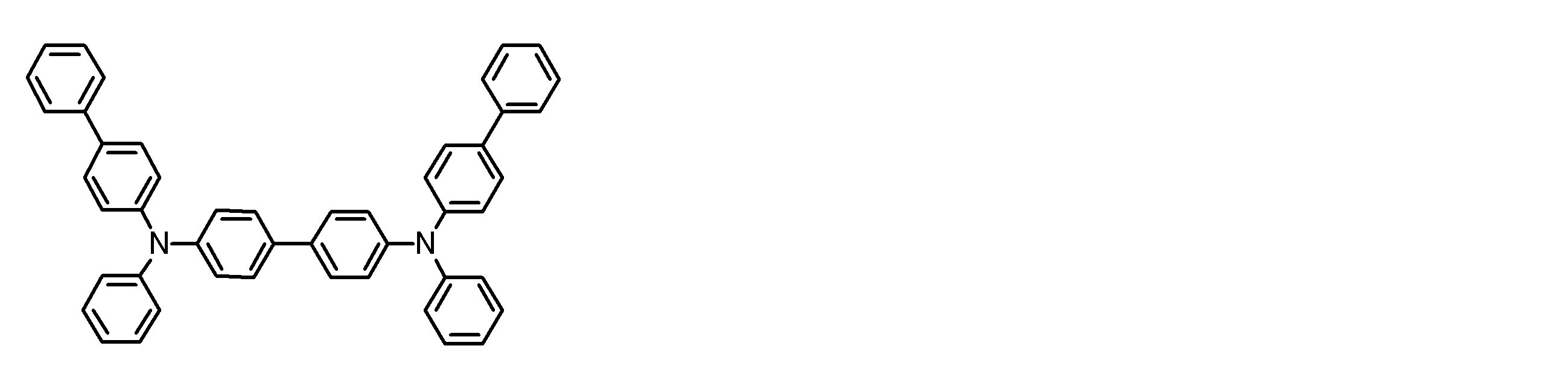
正孔注入層には電子受容性ドーパントを含有することが好ましい。正孔注入層に電子受容性ドーパントを含有することにより、正孔注入性が向上し、駆動電圧が低下する、効率が向上するなどの効果がある。電子受容性ドーパントとは、ドープされる材料から電子を引き抜き、ラジカルカチオンを発生させることが可能な材料であれば有機材料、無機材料のうちいかなるものでもよいが、例えば、テトラシアノキノジメタン(TCNQ)、テトラフルオロテトラシアノキノジメタン(F4-TCNQ)、酸化モリブデンなどが挙げられる。
The hole injection layer preferably contains an electron accepting dopant. By containing an electron-accepting dopant in the hole injection layer, hole injection properties are improved, driving voltage is lowered, and efficiency is improved. The electron-accepting dopant may be any organic material or inorganic material as long as it can extract electrons from the doped material and generate radical cations. For example, tetracyanoquinodimethane ( TCNQ), tetrafluorotetracyanoquinodimethane (F 4 -TCNQ), molybdenum oxide and the like.
正孔注入層中の電子受容性ドーパントは、正孔注入層を形成する全化合物質量に対して、0.01質量%~50質量%含有されることが好ましく、0.1質量%~40質量%含有されることがより好ましく、0.2質量%~30質量%含有されることがより好ましい。
The electron-accepting dopant in the hole injection layer is preferably contained in an amount of 0.01% by mass to 50% by mass, and preferably 0.1% by mass to 40% by mass with respect to the total mass of the compound forming the hole injection layer. %, More preferably 0.2% by mass to 30% by mass.
(A-2)電子ブロック層
電子ブロック層は、陰極側から発光層に輸送された電子が、陽極側に通りぬけることを防止する機能を有する層である。本発明において、発光層と陽極側で隣接する有機層として、電子ブロック層を設けることができる。
電子ブロック層を構成する有機化合物の例としては、例えば前述の正孔輸送材料として挙げたものが適用できる。
電子ブロック層の厚さとしては、1nm~500nmであるのが好ましく、3nm~100nmであるのがより好ましく、5nm~50nmであるのが更に好ましい。
電子ブロック層は、上述した材料の一種又は二種以上からなる単層構造であってもよいし、同一組成又は異種組成の複数層からなる多層構造であってもよい。
電子ブロック層に用いる材料は、前記燐光発光材料のT1エネルギーより高いことが色純度、発光効率、駆動耐久性の点で好ましい。電子ブロック層に用いる材料の膜状態でのT1が燐光発光材料のT1より0.1eV以上大きいことが好ましく、0.2eV以上大きいことがより好ましく、0.3eV以上大きいことが更に好ましい。 (A-2) Electron Blocking Layer The electron blocking layer is a layer having a function of preventing electrons transported from the cathode side to the light emitting layer from passing through to the anode side. In the present invention, an electron blocking layer can be provided as an organic layer adjacent to the light emitting layer on the anode side.
As an example of the organic compound constituting the electron blocking layer, for example, those mentioned as the hole transport material described above can be applied.
The thickness of the electron blocking layer is preferably 1 nm to 500 nm, more preferably 3 nm to 100 nm, and even more preferably 5 nm to 50 nm.
The electron blocking layer may have a single layer structure composed of one or more of the above-described materials, or may have a multilayer structure composed of a plurality of layers having the same composition or different compositions.
The material used for the electron blocking layer is preferably higher than the T 1 energy of the phosphorescent material in terms of color purity, luminous efficiency, and driving durability. It is preferable T 1 is greater than 0.1eV than T 1 of the phosphorescent material in the film state of the material used for the electron blocking layer, it is more preferably at least 0.2eV higher, and further preferably more than 0.3eV large.
(B)陰極と前記発光層との間に好ましく配置される有機層
次に、前記(B)陰極と前記発光層との間に好ましく配置される有機層について説明する。 (B) Organic layer preferably disposed between the cathode and the light emitting layer Next, the (B) organic layer preferably disposed between the cathode and the light emitting layer will be described.
次に、前記(B)陰極と前記発光層との間に好ましく配置される有機層について説明する。 (B) Organic layer preferably disposed between the cathode and the light emitting layer Next, the (B) organic layer preferably disposed between the cathode and the light emitting layer will be described.
(B-1)電子注入層、電子輸送層
電子注入層、電子輸送層は、陰極又は陰極側から電子を受け取り陽極側に輸送する機能を有する層である。これらの層に用いる電子注入材料、電子輸送材料は低分子化合物であっても高分子化合物であってもよい。
電子輸送材料として、前記一般式(1)で表される化合物を用いることができ、その好ましい態様は、上述の一般式(1)で表される化合物を発光層以外の層に含有させる場合の説明のとおりである。その他の電子輸送材料としては、ピリジン誘導体、キノリン誘導体、ピリミジン誘導体、ピラジン誘導体、フタラジン誘導体、フェナントロリン誘導体、トリアジン誘導体、トリアゾール誘導体、オキサゾール誘導体、オキサジアゾール誘導体、イミダゾール誘導体、フルオレノン誘導体、アントラキノジメタン誘導体、アントロン誘導体、ジフェニルキノン誘導体、チオピランジオキシド誘導体、カルボジイミド誘導体、フルオレニリデンメタン誘導体、ジスチリルピラジン誘導体、ナフタレン、ペリレン等の芳香環テトラカルボン酸無水物、フタロシアニン誘導体、8-キノリノール誘導体の金属錯体やメタルフタロシアニン、ベンゾオキサゾールやベンゾチアゾールを配位子とする金属錯体に代表される各種金属錯体、シロールに代表される有機シラン誘導体、等を含有する層であることが好ましい。 (B-1) Electron Injection Layer, Electron Transport Layer The electron injection layer and the electron transport layer are layers having a function of receiving electrons from the cathode or the cathode side and transporting them to the anode side. The electron injection material and the electron transport material used for these layers may be a low molecular compound or a high molecular compound.
As the electron transport material, the compound represented by the general formula (1) can be used, and a preferable embodiment thereof is a case where the compound represented by the general formula (1) is contained in a layer other than the light emitting layer. As explained. Other electron transport materials include pyridine derivatives, quinoline derivatives, pyrimidine derivatives, pyrazine derivatives, phthalazine derivatives, phenanthroline derivatives, triazine derivatives, triazole derivatives, oxazole derivatives, oxadiazole derivatives, imidazole derivatives, fluorenone derivatives, anthraquinodimethane. Derivatives, anthrone derivatives, diphenylquinone derivatives, thiopyran dioxide derivatives, carbodiimide derivatives, fluorenylidenemethane derivatives, distyrylpyrazine derivatives, aromatic ring tetracarboxylic anhydrides such as naphthalene and perylene, phthalocyanine derivatives, 8-quinolinol derivatives Represented by metal complexes, metal phthalocyanines, various metal complexes represented by metal complexes with benzoxazole and benzothiazole ligands, and siloles Organosilane derivatives, a layer containing such is preferable.
電子注入層、電子輸送層の厚さは、駆動電圧を下げるという観点から、各々500nm以下であることが好ましい。
電子輸送層の厚さとしては、1nm~500nmであるのが好ましく、5nm~200nmであるのがより好ましく、10nm~100nmであるのが更に好ましい。また、電子注入層の厚さとしては、0.1nm~200nmであるのが好ましく、0.2nm~100nmであるのがより好ましく、0.5nm~50nmであるのが更に好ましい。
電子注入層、電子輸送層は、上述した材料の1種又は2種以上からなる単層構造であってもよいし、同一組成又は異種組成の複数層からなる多層構造であってもよい。 The thicknesses of the electron injection layer and the electron transport layer are each preferably 500 nm or less from the viewpoint of lowering the driving voltage.
The thickness of the electron transport layer is preferably 1 nm to 500 nm, more preferably 5 nm to 200 nm, and even more preferably 10 nm to 100 nm. The thickness of the electron injection layer is preferably from 0.1 nm to 200 nm, more preferably from 0.2 nm to 100 nm, and even more preferably from 0.5 nm to 50 nm.
The electron injection layer and the electron transport layer may have a single layer structure composed of one or more of the above-described materials, or may have a multilayer structure composed of a plurality of layers having the same composition or different compositions.
電子注入層には電子供与性ドーパントを含有することが好ましい。電子注入層に電子供与性ドーパントを含有させることにより、電子注入性が向上し、駆動電圧が低下する、効率が向上するなどの効果がある。電子供与性ドーパントとは、ドープされる材料に電子を与え、ラジカルアニオンを発生させることが可能な材料であれば有機材料、無機材料のうちいかなるものでもよいが、例えば、テトラチアフルバレン(TTF)、テトラチアナフタセン(TTT)、ビス-[1,3 ジエチル-2-メチル-1,2-ジヒドロベンズイミダゾリル]などのジヒドロイミダゾール化合物、リチウム、セシウムなどが挙げられる。
The electron injection layer preferably contains an electron donating dopant. By including an electron donating dopant in the electron injection layer, the electron injection property is improved, the driving voltage is lowered, and the efficiency is improved. The electron donating dopant may be any organic material or inorganic material as long as it can give electrons to the doped material and generate radical anions. For example, tetrathiafulvalene (TTF) And dithiaimidazole compounds such as tetrathianaphthacene (TTT) and bis- [1,3 diethyl-2-methyl-1,2-dihydrobenzimidazolyl], lithium, cesium and the like.
電子注入層中の電子供与性ドーパントは、電子注入層を形成する全化合物質量に対して、0.01質量%~50質量%含有されることが好ましく、0.1質量%~40質量%含有されることがより好ましく、0.5質量%~30質量%含有されることがより好ましい。
The electron donating dopant in the electron injection layer is preferably contained in an amount of 0.01% by mass to 50% by mass, and 0.1% by mass to 40% by mass with respect to the total mass of the compound forming the electron injection layer. More preferably, the content is 0.5 to 30% by mass.
(B-2)正孔ブロック層
正孔ブロック層は、陽極側から発光層に輸送された正孔が、陰極側に通りぬけることを防止する機能を有する層である。本発明において、発光層と陰極側で隣接する有機層として、正孔ブロック層を設けることができる。
正孔ブロック層を構成する有機化合物の膜状態でのT1エネルギーは、発光層で生成する励起子のエネルギー移動を防止し、発光効率を低下させないために、発光材料のT1エネルギーよりも高いことが好ましい。
正孔ブロック層を構成する有機化合物の例としては、前記一般式(1)で表される化合物を用いることができる。
前記一般式(1)で表される化合物以外の、正孔ブロック層を構成するその他の有機化合物の例としては、アルミニウム(III)ビス(2-メチル-8-キノリナト)4-フェニルフェノレート(Aluminum (III)bis(2-methyl-8-quinolinato)4-phenylphenolate(Balqと略記する))等のアルミニウム錯体、トリアゾール誘導体、2,9-ジメチル-4,7-ジフェニル-1,10-フェナントロリン(2,9-Dimethyl-4,7-diphenyl-1,10-phenanthroline(BCPと略記する))等のフェナントロリン誘導体、本発明の化合物等が挙げられる。本発明において、正孔ブロック層は実際に正孔をブロックする機能に限定せず、発光層の励起子が電子輸送層に拡散させない、若しくはエネルギー移動消光をブロックする機能を有していてもよい。本発明の化合物は正孔ブロック層としても好ましく適用できる。
正孔ブロック層の厚さとしては、1nm~500nmであるのが好ましく、5nm~200nmであるのがより好ましく、10nm~100nmであるのが更に好ましい。
正孔ブロック層は、上述した材料の一種又は二種以上からなる単層構造であってもよいし、同一組成又は異種組成の複数層からなる多層構造であってもよい。
正孔ブロック層に用いる材料は、前記燐光発光材料のT1エネルギーより高いことが色純度、発光効率、駆動耐久性の点で好ましい。正孔ブロック層に用いる材料の膜状態でのT1が燐光発光材料のT1より0.1eV以上大きいことが好ましく、0.2eV以上大きいことがより好ましく、0.3eV以上大きいことが更に好ましい。 (B-2) Hole blocking layer The hole blocking layer is a layer having a function of preventing holes transported from the anode side to the light emitting layer from passing through to the cathode side. In the present invention, a hole blocking layer can be provided as an organic layer adjacent to the light emitting layer on the cathode side.
The T 1 energy in the film state of the organic compound constituting the hole blocking layer is higher than the T 1 energy of the light emitting material in order to prevent energy transfer of excitons generated in the light emitting layer and not to reduce the light emission efficiency. It is preferable.
As an example of the organic compound constituting the hole blocking layer, the compound represented by the general formula (1) can be used.
Examples of other organic compounds constituting the hole blocking layer other than the compound represented by the general formula (1) include aluminum (III) bis (2-methyl-8-quinolinato) 4-phenylphenolate ( Aluminum complexes such as aluminum (III) bis (2-methyl-8-quinolinato) 4-phenylphenolate (abbreviated as Balq)), triazole derivatives, 2,9-dimethyl-4,7-diphenyl-1,10-phenanthroline ( And phenanthroline derivatives such as 2,9-Dimethyl-4,7-diphenyl-1,10-phenanthroline (abbreviated as BCP)) and the compounds of the present invention. In the present invention, the hole blocking layer is not limited to the function of actually blocking holes, and the exciton of the light emitting layer may not diffuse into the electron transport layer, or may have a function of blocking energy transfer quenching. . The compound of the present invention can also be preferably applied as a hole blocking layer.
The thickness of the hole blocking layer is preferably 1 nm to 500 nm, more preferably 5 nm to 200 nm, and even more preferably 10 nm to 100 nm.
The hole blocking layer may have a single layer structure made of one or more of the materials described above, or may have a multilayer structure made of a plurality of layers having the same composition or different compositions.
The material used for the hole blocking layer is preferably higher than the T 1 energy of the phosphorescent light emitting material in terms of color purity, light emission efficiency, and driving durability. Holes T 1 of the at film state of the material used in the blocking layer is preferably greater 0.1eV higher than the T 1 of the phosphorescent material, more preferably at least 0.2eV higher, and further preferably more than 0.3eV greater .
(B-3)陰極と前記発光層との間に好ましく配置される有機層に特に好ましく用いられる材料
本発明の有機電界発光素子は、前記(B)陰極と前記発光層との間に好ましく配置される有機層の材料に特に好ましく用いられる材料として、前記一般式(1)で表される化合物および下記一般式(O-1)で表される化合物を挙げることができる。
以下、前記一般式(O-1)で表される化合物について説明する。 (B-3) Material particularly preferably used for the organic layer preferably disposed between the cathode and the light emitting layer The organic electroluminescent element of the present invention is preferably disposed between the (B) cathode and the light emitting layer. As a material that is particularly preferably used for the material of the organic layer, a compound represented by the general formula (1) and a compound represented by the following general formula (O-1) can be given.
Hereinafter, the compound represented by the general formula (O-1) will be described.
本発明の有機電界発光素子は、発光層と陰極との間に少なくとも一層の有機層を含むことが好ましく、該有機層に少なくとも一種の下記一般式(O-1)で表される化合物を含有することが素子の効率や駆動電圧の観点から好ましい。以下に、一般式(O-1)について説明する。
The organic electroluminescent device of the present invention preferably includes at least one organic layer between the light emitting layer and the cathode, and the organic layer contains at least one compound represented by the following general formula (O-1). It is preferable from the viewpoint of device efficiency and driving voltage. The general formula (O-1) will be described below.

(一般式(O-1)中、RO1は、アルキル基、アリール基、又はヘテロアリール基を表す。AO1~AO4はそれぞれ独立に、C-RA又は窒素原子を表す。RAは水素原子、アルキル基、アリール基、又はヘテロアリール基を表し、複数のRAは同じでも異なっていても良い。LO1は、アリール環又はヘテロアリール環からなる二価~六価の連結基を表す。nO1は2~6の整数を表す。)
(In the general formula (O1), R O1 represents an alkyl group, an aryl group, or each independently .A O1 ~ A O4 representing the heteroaryl group, the C-R A or .R A representing the nitrogen atom Represents a hydrogen atom, an alkyl group, an aryl group, or a heteroaryl group, and a plurality of R A may be the same or different, L O1 represents a divalent to hexavalent linking group comprising an aryl ring or a heteroaryl ring; N O1 represents an integer of 2 to 6.)
RO1は、アルキル基(好ましくは炭素数1~8)、アリール基(好ましくは炭素数6~30)、又はヘテロアリール基(好ましくは炭素数4~12)を表し、これらは前述の置換基群Aから選ばれる置換基を有していても良い。RO1として好ましくはアリール基、又はヘテロアリール基であり、より好ましくはアリール基である。RO1のアリール基が置換基を有する場合の好ましい置換基としては、アルキル基、アリール基又はシアノ基が挙げられ、アルキル基又はアリール基がより好ましく、アリール基が更に好ましい。RO1のアリール基が複数の置換基を有する場合、該複数の置換基は互いに結合して5又は6員環を形成していても良い。RO1のアリール基は、好ましくは置換基群Aから選ばれる置換基を有していても良いフェニル基であり、より好ましくはアルキル基又はアリール基が置換していてもよいフェニル基であり、更に好ましくは無置換のフェニル基又は2-フェニルフェニル基である。
R O1 represents an alkyl group (preferably having 1 to 8 carbon atoms), an aryl group (preferably having 6 to 30 carbon atoms), or a heteroaryl group (preferably having 4 to 12 carbon atoms). It may have a substituent selected from group A. R O1 is preferably an aryl group or a heteroaryl group, more preferably an aryl group. A preferable substituent when the aryl group of R O1 has a substituent includes an alkyl group, an aryl group or a cyano group, more preferably an alkyl group or an aryl group, and still more preferably an aryl group. When the aryl group of R O1 has a plurality of substituents, the plurality of substituents may be bonded to each other to form a 5- or 6-membered ring. The aryl group of R O1 is preferably a phenyl group which may have a substituent selected from the substituent group A, more preferably a phenyl group which may be substituted with an alkyl group or an aryl group, More preferred is an unsubstituted phenyl group or 2-phenylphenyl group.
AO1~AO4はそれぞれ独立に、C-RA又は窒素原子を表す。AO1~AO4のうち、0~2つが窒素原子であるのが好ましく、0又は1つが窒素原子であるのがより好ましい。AO1~AO4の全てがC-RAであるか、又はAO1が窒素原子で、AO2~AO4がC-RAであるのが好ましく、AO1が窒素原子で、AO2~AO4がC-RAであるのがより好ましく、AO1が窒素原子で、AO2~AO4がC-RAであり、RAが全て水素原子であるのが更に好ましい。
A O1 to A O4 each independently represent C—R A or a nitrogen atom. Of A O1 to A O4 , 0 to 2 are preferably nitrogen atoms, more preferably 0 or 1 is a nitrogen atom. Or all of A O1 ~ A O4 is C-R A, or A O1 be a nitrogen atom, is preferably A O2 ~ A O4 is C-R A, A O1 be a nitrogen atom, A O2 ~ More preferably, A O4 is C—R A , A O1 is a nitrogen atom, A O2 to A O4 are C—R A , and R A is all hydrogen atoms.
RAは水素原子、アルキル基(好ましくは炭素数1~8)、アリール基(好ましくは炭素数6~30)、又はヘテロアリール基(好ましくは炭素数4~12)を表し、これらは前述の置換基群Aから選ばれる置換基を有していても良い。また複数のRAは同じでも異なっていても良い。RAとして好ましくは水素原子又はアルキル基であり、より好ましくは水素原子である。
R A represents a hydrogen atom, an alkyl group (preferably having a carbon number of 1 to 8), an aryl group (preferably having a carbon number of 6 to 30), or a heteroaryl group (preferably having a carbon number of 4 to 12). It may have a substituent selected from the substituent group A. The plurality of R A may be the same or different. R A is preferably a hydrogen atom or an alkyl group, more preferably a hydrogen atom.
LO1は、アリール環(好ましくは炭素数6~30)又はヘテロアリール環(好ましくは炭素数4~12)からなる二価~六価の連結基を表す。LO1として好ましくは、アリーレン基、ヘテロアリーレン基、アリールトリイル基、又はヘテロアリールトリイル基であり、より好ましくはフェニレン基、ビフェニレン基、又はベンゼントリイル基であり、更に好ましくはビフェニレン基、又はベンゼントリイル基である。LO1は前述の置換基群Aから選ばれる置換基を有していても良く、置換基を有する場合の置換基としてはアルキル基、アリール基、又はシアノ基が好ましい。LO1の具体例としては、以下のものが挙げられる。
L O1 represents a divalent to hexavalent linking group consisting of an aryl ring (preferably having 6 to 30 carbon atoms) or a heteroaryl ring (preferably having 4 to 12 carbon atoms). L O1 is preferably an arylene group, heteroarylene group, aryltriyl group, or heteroaryltriyl group, more preferably a phenylene group, a biphenylene group, or a benzenetriyl group, still more preferably a biphenylene group, Or it is a benzenetriyl group. L O1 may have a substituent selected from the aforementioned substituent group A, and the alkyl group, aryl group, or cyano group is preferred as the substituent when it has a substituent. Specific examples of L O1 include the following.
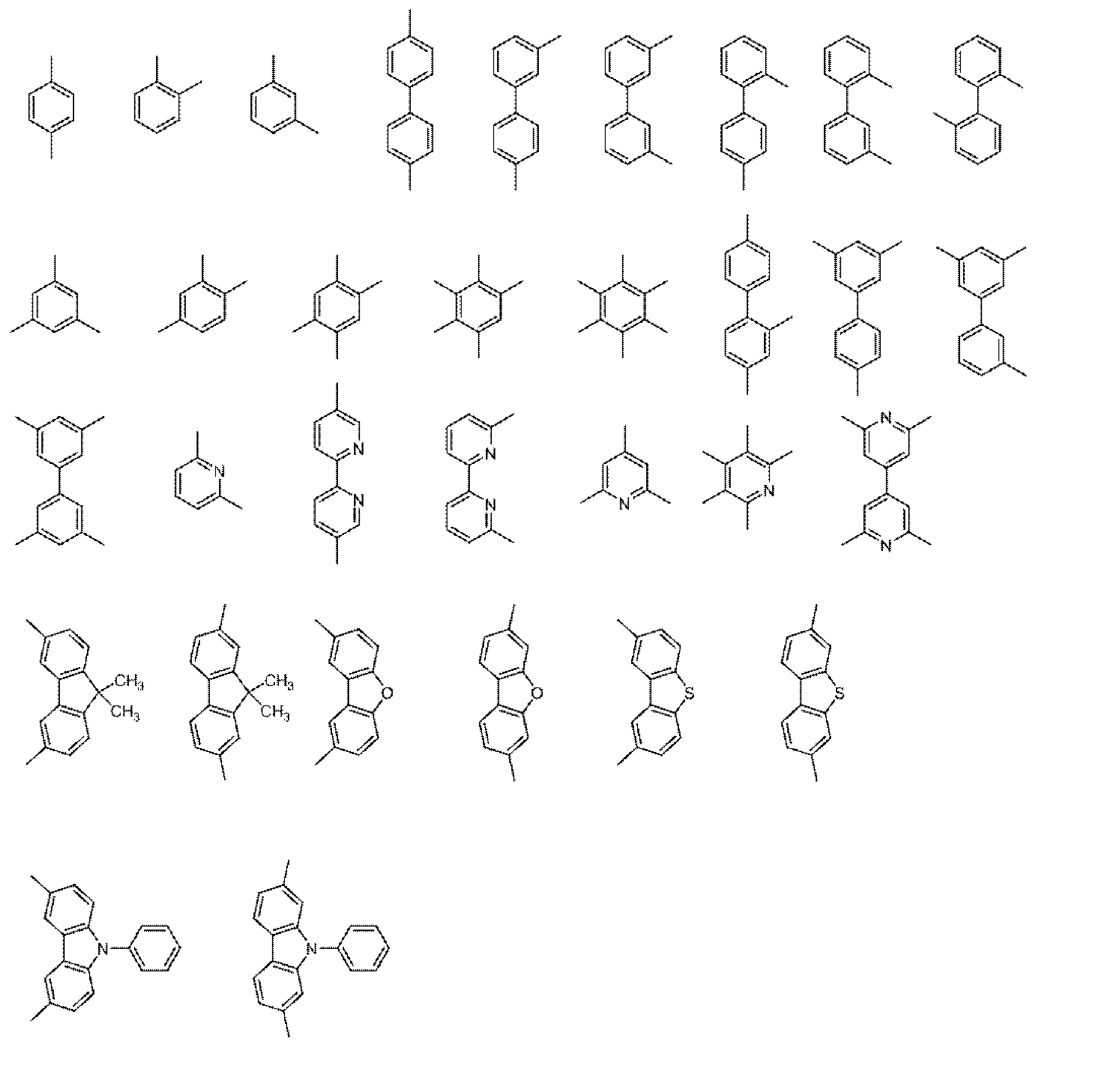
nO1は2~6の整数を表し、好ましくは2~4の整数であり、より好ましくは2又は3である。nO1は、素子効率の観点では最も好ましくは3であり、素子の耐久性の観点では最も好ましくは2である。
一般式(O-1)で表される化合物は、より好ましくは下記一般式(O-2)で表される化合物である。 n O1 represents an integer of 2 to 6, preferably an integer of 2 to 4, more preferably 2 or 3. n O1 is most preferably 3 in terms of device efficiency, and most preferably 2 in terms of device durability.
The compound represented by the general formula (O-1) is more preferably a compound represented by the following general formula (O-2).
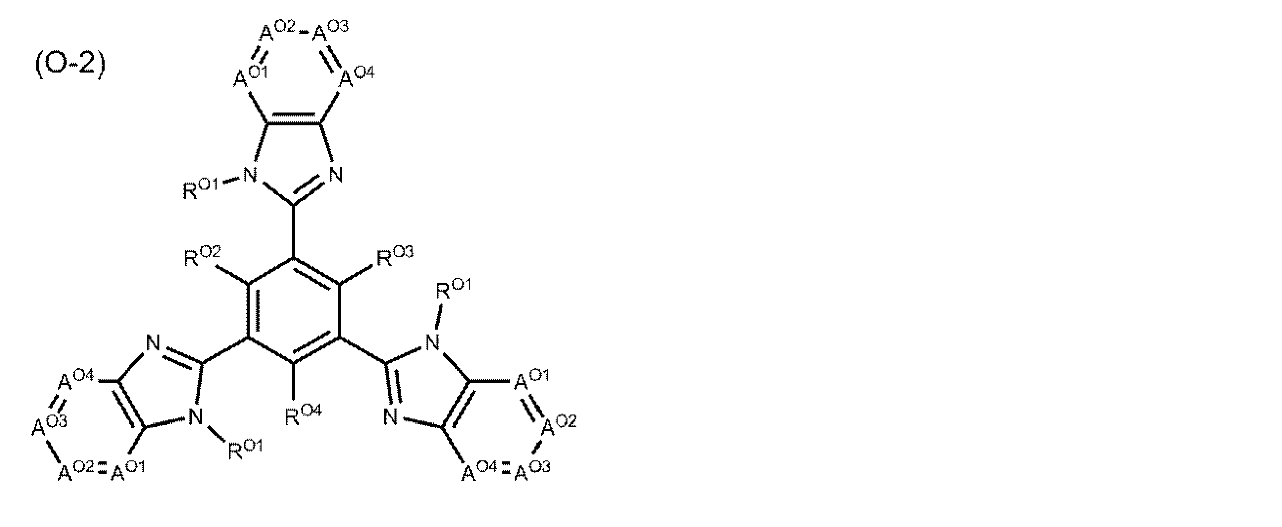
(一般式(O-2)中、RO1はアルキル基、アリール基、又はヘテロアリール基を表す。RO2~RO4はそれぞれ独立に、水素原子、アルキル基、アリール基、又はヘテロアリール基を表す。AO1~AO4はそれぞれ独立に、C-RA又は窒素原子を表す。RAは水素原子、アルキル基、アリール基、又はヘテロアリール基を表し、複数のRAは同じでも異なっていても良い。)
(In the general formula (O-2), R O1 represents an alkyl group, an aryl group, or a heteroaryl group. R O2 to R O4 each independently represents a hydrogen atom, an alkyl group, an aryl group, or a heteroaryl group. A O1 to A O4 each independently represent C—R A or a nitrogen atom, R A represents a hydrogen atom, an alkyl group, an aryl group, or a heteroaryl group, and a plurality of R A are the same or different. May be.)
RO1及びAO1~AO4は、前記一般式(O-1)中のRO1及びAO1~AO4と同義であり、またそれらの好ましい範囲も同様である。
R02~R04はそれぞれ独立に、水素原子、アルキル基(好ましくは炭素数1~8)、アリール基(好ましくは炭素数6~30)、又はヘテロアリール基(好ましくは炭素数4~12)を表し、これらは前述の置換基群Aから選ばれる置換基を有していても良い。R02~R04として好ましくは水素原子、アルキル基、又はアリール基であり、より好ましくは水素原子、又はアリール基であり、最も好ましくは水素原子である。 R O1 and A O1 ~ A O4, the general formula (O1) in the same meaning as R O1 and A O1 ~ A O4 of, also the same preferable ranges thereof.
R 02 to R 04 are each independently a hydrogen atom, an alkyl group (preferably having 1 to 8 carbon atoms), an aryl group (preferably having 6 to 30 carbon atoms), or a heteroaryl group (preferably having 4 to 12 carbon atoms). These may have a substituent selected from the aforementioned substituent group A. R 02 to R 04 are preferably a hydrogen atom, an alkyl group, or an aryl group, more preferably a hydrogen atom or an aryl group, and most preferably a hydrogen atom.
前記一般式(O-1)で表される化合物は、高温保存時の安定性、高温駆動時、駆動時の発熱に対して安定して動作させる観点から、ガラス転移温度(Tg)は100℃~300℃であることが好ましく、120℃~300℃であることがより好ましく、120℃~300℃であることが更に好ましく、140℃~300℃であることが更により好ましい。
The compound represented by the general formula (O-1) has a glass transition temperature (Tg) of 100 ° C. from the viewpoint of stable operation at high temperature storage, stable operation against high temperature driving, and heat generation during driving. It is preferably from ˜300 ° C., more preferably from 120 ° C. to 300 ° C., further preferably from 120 ° C. to 300 ° C., and still more preferably from 140 ° C. to 300 ° C.
一般式(O-1)で表される化合物の具体例を以下に示すが、本発明はこれらに限定されない。
Specific examples of the compound represented by the general formula (O-1) are shown below, but the present invention is not limited thereto.

前記一般式(O-1)で表される化合物は、特開2001-335776号に記載の方法で合成可能である。合成後、カラムクロマトグラフィー、再結晶、再沈殿などによる精製を行った後、昇華精製により精製することが好ましい。昇華精製により有機不純物を分離できるだけではなく、無機塩や残留溶媒、水分等を効果的に取り除くことが可能である。
The compound represented by the general formula (O-1) can be synthesized by the method described in JP-A No. 2001-335776. After synthesis, purification by column chromatography, recrystallization, reprecipitation, etc., followed by purification by sublimation is preferred. Not only can organic impurities be separated by sublimation purification, but inorganic salts, residual solvents, moisture, and the like can be effectively removed.
本発明の有機電界発光素子において、一般式(O-1)で表される化合物は発光層と陰極との間の有機層に含有されることが好ましいが、発光層に隣接する陰極側の層に含有されることがより好ましい。
一般式(O-1)で表される化合物は、添加する有機層の全質量に対して70~100質量%含まれることが好ましく、85~100質量%含まれることがより好ましい。 In the organic electroluminescent device of the present invention, the compound represented by the general formula (O-1) is preferably contained in the organic layer between the light emitting layer and the cathode, but the cathode side layer adjacent to the light emitting layer is used. It is more preferable that it is contained.
The compound represented by the general formula (O-1) is preferably contained in an amount of 70 to 100% by mass, and more preferably 85 to 100% by mass with respect to the total mass of the organic layer to be added.
<保護層>
本発明において、有機電界発光素子全体は、保護層によって保護されていてもよい。
保護層については、特開2008-270736号公報の段落番号〔0169〕~〔0170〕に記載の事項を本発明に適用することができる。なお、保護層の材料は無機物であっても、有機物であってもよい。 <Protective layer>
In the present invention, the entire organic electroluminescent element may be protected by a protective layer.
As for the protective layer, the matters described in JP-A-2008-270736, paragraphs [0169] to [0170] can be applied to the present invention. The material for the protective layer may be inorganic or organic.
<封止容器>
本発明の有機電界発光素子は、封止容器を用いて素子全体を封止してもよい。
封止容器については、特開2008-270736号公報の段落番号〔0171〕に記載の事項を本発明に適用することができる。 <Sealing container>
The organic electroluminescent element of the present invention may be sealed entirely using a sealing container.
Regarding the sealing container, the matters described in paragraph [0171] of JP-A-2008-270736 can be applied to the present invention.
(駆動方法)
本発明の有機電界発光素子は、陽極と陰極との間に直流(必要に応じて交流成分を含んでもよい)電圧(通常2ボルト~15ボルト)、又は直流電流を印加することにより、発光を得ることができる。
本発明の有機電界発光素子の駆動方法については、特開平2-148687号、同6-301355号、同5-29080号、同7-134558号、同8-234685号、同8-241047号の各公報、特許第2784615号、米国特許5828429号、同6023308号の各明細書等に記載の駆動方法を適用することができる。 (Driving method)
The organic electroluminescence device of the present invention emits light by applying a direct current (which may include an alternating current component as necessary) voltage (usually 2 to 15 volts) or a direct current between the anode and the cathode. Obtainable.
The driving method of the organic electroluminescence device of the present invention is described in JP-A-2-148687, JP-A-6-301355, JP-A-5-290080, JP-A-7-134558, JP-A-8-234585, and JP-A-8-2441047. The driving methods described in each publication, Japanese Patent No. 2784615, US Pat. Nos. 5,828,429 and 6,023,308 can be applied.
本発明の有機電界発光素子の外部量子効率としては、7%以上が好ましく、10%以上がより好ましく、12%以上が更に好ましい。外部量子効率の数値は20℃で素子を駆動したときの外部量子効率の最大値、若しくは、20℃で素子を駆動したときの300~400cd/m2付近での外部量子効率の値を用いることができる。
The external quantum efficiency of the organic electroluminescent element of the present invention is preferably 7% or more, more preferably 10% or more, and further preferably 12% or more. The value of the external quantum efficiency should be the maximum value of the external quantum efficiency when the device is driven at 20 ° C., or the value of the external quantum efficiency in the vicinity of 300 to 400 cd / m 2 when the device is driven at 20 ° C. Can do.
本発明の有機電界発光素子の内部量子効率は、30%以上であることが好ましく、50%以上が更に好ましく、70%以上が更に好ましい。素子の内部量子効率は、外部量子効率を光取り出し効率で除して算出される。通常の有機EL素子では光取り出し効率は約20%であるが、基板の形状、電極の形状、有機層の膜厚、無機層の膜厚、有機層の屈折率、無機層の屈折率等を工夫することにより、光取り出し効率を20%以上にすることが可能である。
The internal quantum efficiency of the organic electroluminescence device of the present invention is preferably 30% or more, more preferably 50% or more, and further preferably 70% or more. The internal quantum efficiency of the device is calculated by dividing the external quantum efficiency by the light extraction efficiency. In a normal organic EL element, the light extraction efficiency is about 20%. However, the shape of the substrate, the shape of the electrode, the thickness of the organic layer, the thickness of the inorganic layer, the refractive index of the organic layer, the refractive index of the inorganic layer, etc. By devising it, it is possible to increase the light extraction efficiency to 20% or more.
<発光ピーク波長>
本発明の有機電界発光素子は、その発光ピーク波長に制限はない。例えば、光の三原色のうち、赤色の発光に用いても、緑色の発光に用いても、青色の発光に用いてもよい。その中でも、本発明の有機電界発光素子は、発光ピーク波長が500~700nmであることが、前記一般式(1)で表される化合物の最低励起三重項(T1)エネルギーの観点から好ましい。
具体的には、本発明の有機電界発光素子において、前記一般式(1)で表される化合物を発光層のホスト材料として用いる場合は、発光ピーク波長が500~700nmであることが好ましく、520~650nmであることがより好ましく、520~550nmであることが特に好ましい。
一方、本発明の有機電界発光素子において、前記一般式(1)で表される化合物を正孔ブロック層の電荷輸送材料として用いる場合は、発光ピーク波長が400~700nmであることが好ましく、450~650nmであることがより好ましく、500~650nmであることが特に好ましい。 <Peak emission wavelength>
The organic electroluminescent element of the present invention has no limitation on the emission peak wavelength. For example, among the three primary colors of light, it may be used for red light emission, green light emission, or blue light emission. Among them, the organic electroluminescence device of the present invention preferably has an emission peak wavelength of 500 to 700 nm from the viewpoint of the lowest excited triplet (T 1 ) energy of the compound represented by the general formula (1).
Specifically, in the organic electroluminescent device of the present invention, when the compound represented by the general formula (1) is used as the host material of the light emitting layer, the emission peak wavelength is preferably 500 to 700 nm. It is more preferably from ˜650 nm, particularly preferably from 520 to 550 nm.
On the other hand, in the organic electroluminescence device of the present invention, when the compound represented by the general formula (1) is used as a charge transport material for the hole blocking layer, the emission peak wavelength is preferably 400 to 700 nm, It is more preferably from ˜650 nm, particularly preferably from 500 to 650 nm.
<本発明の有機電界発光素子の用途>
本発明の有機電界発光素子は、表示素子、ディスプレイ、バックライト、電子写真、照明光源、記録光源、露光光源、読み取り光源、標識、看板、インテリア、又は光通信等に好適に利用できる。特に、発光装置、照明装置、表示装置等の発光輝度が高い領域で駆動されるデバイスに好ましく用いられる。 <Use of the organic electroluminescent device of the present invention>
The organic electroluminescent element of the present invention can be suitably used for a display element, a display, a backlight, an electrophotography, an illumination light source, a recording light source, an exposure light source, a reading light source, a sign, a signboard, an interior, or optical communication. In particular, it is preferably used for a device that is driven in a region where light emission luminance is high, such as a light emitting device, a lighting device, and a display device.
[発光装置]
本発明の発光装置は、本発明の有機電界発光素子を含むことを特徴とする。
次に、図2を参照して本発明の発光装置について説明する。
本発明の発光装置は、前記有機電界発光素子を用いてなる。
図2は、本発明の発光装置の一例を概略的に示した断面図である。図2の発光装置20は、基板(支持基板)2、有機電界発光素子10、封止容器16等により構成されている。 [Light emitting device]
The light emitting device of the present invention includes the organic electroluminescent element of the present invention.
Next, the light emitting device of the present invention will be described with reference to FIG.
The light emitting device of the present invention uses the organic electroluminescent element.
FIG. 2 is a cross-sectional view schematically showing an example of the light emitting device of the present invention. The light-emittingdevice 20 of FIG. 2 is comprised by the board | substrate (support substrate) 2, the organic electroluminescent element 10, the sealing container 16, etc. FIG.
本発明の発光装置は、本発明の有機電界発光素子を含むことを特徴とする。
次に、図2を参照して本発明の発光装置について説明する。
本発明の発光装置は、前記有機電界発光素子を用いてなる。
図2は、本発明の発光装置の一例を概略的に示した断面図である。図2の発光装置20は、基板(支持基板)2、有機電界発光素子10、封止容器16等により構成されている。 [Light emitting device]
The light emitting device of the present invention includes the organic electroluminescent element of the present invention.
Next, the light emitting device of the present invention will be described with reference to FIG.
The light emitting device of the present invention uses the organic electroluminescent element.
FIG. 2 is a cross-sectional view schematically showing an example of the light emitting device of the present invention. The light-emitting
有機電界発光素子10は、基板2上に、陽極(第一電極)3、有機層11、陰極(第二電極)9が順次積層されて構成されている。また、陰極9上には、保護層12が積層されており、更に、保護層12上には接着層14を介して封止容器16が設けられている。なお、各電極3、9の一部、隔壁、絶縁層等は省略されている。
ここで、接着層14としては、エポキシ樹脂等の光硬化型接着剤や熱硬化型接着剤を用いることができ、例えば熱硬化性の接着シートを用いることもできる。 Theorganic electroluminescent device 10 is configured by sequentially laminating an anode (first electrode) 3, an organic layer 11, and a cathode (second electrode) 9 on a substrate 2. A protective layer 12 is laminated on the cathode 9, and a sealing container 16 is provided on the protective layer 12 with an adhesive layer 14 interposed therebetween. In addition, a part of each electrode 3 and 9, a partition, an insulating layer, etc. are abbreviate | omitted.
Here, as theadhesive layer 14, a photocurable adhesive such as an epoxy resin or a thermosetting adhesive can be used, and for example, a thermosetting adhesive sheet can also be used.
ここで、接着層14としては、エポキシ樹脂等の光硬化型接着剤や熱硬化型接着剤を用いることができ、例えば熱硬化性の接着シートを用いることもできる。 The
Here, as the
本発明の発光装置の用途は特に制限されるものではなく、例えば、照明装置のほか、テレビ、パーソナルコンピュータ、携帯電話、電子ペーパ等の表示装置とすることができる。
The use of the light-emitting device of the present invention is not particularly limited, and for example, it can be a display device such as a television, a personal computer, a mobile phone, and electronic paper in addition to a lighting device.
[照明装置]
本発明の照明装置は、本発明の有機電界発光素子を含むことを特徴とする。
次に、図3を参照して本発明の照明装置について説明する。
図3は、本発明の照明装置の一例を概略的に示した断面図である。本発明の照明装置40は、図3に示すように、前述した有機EL素子10と、光散乱部材30とを備えている。より具体的には、照明装置40は、有機EL素子10の基板2と光散乱部材30とが接触するように構成されている。
光散乱部材30は、光を散乱できるものであれば特に制限されないが、図3においては、透明基板31に微粒子32が分散した部材とされている。透明基板31としては、例えば、ガラス基板を好適に挙げることができる。微粒子32としては、透明樹脂微粒子を好適に挙げることができる。ガラス基板及び透明樹脂微粒子としては、いずれも、公知のものを使用できる。このような照明装置40は、有機電界発光素子10からの発光が散乱部材30の光入射面30Aに入射されると、入射光を光散乱部材30により散乱させ、散乱光を光出射面30Bから照明光として出射するものである。 [Lighting device]
The illuminating device of this invention is characterized by including the organic electroluminescent element of this invention.
Next, the illumination device of the present invention will be described with reference to FIG.
FIG. 3 is a cross-sectional view schematically showing an example of the illumination device of the present invention. As shown in FIG. 3, theillumination device 40 of the present invention includes the organic EL element 10 and the light scattering member 30 described above. More specifically, the lighting device 40 is configured such that the substrate 2 of the organic EL element 10 and the light scattering member 30 are in contact with each other.
Thelight scattering member 30 is not particularly limited as long as it can scatter light. In FIG. 3, the light scattering member 30 is a member in which fine particles 32 are dispersed on a transparent substrate 31. As the transparent substrate 31, for example, a glass substrate can be preferably cited. As the fine particles 32, transparent resin fine particles can be preferably exemplified. As the glass substrate and the transparent resin fine particles, known ones can be used. In such an illuminating device 40, when light emitted from the organic electroluminescent element 10 is incident on the light incident surface 30A of the scattering member 30, the incident light is scattered by the light scattering member 30, and the scattered light is emitted from the light emitting surface 30B. It is emitted as illumination light.
本発明の照明装置は、本発明の有機電界発光素子を含むことを特徴とする。
次に、図3を参照して本発明の照明装置について説明する。
図3は、本発明の照明装置の一例を概略的に示した断面図である。本発明の照明装置40は、図3に示すように、前述した有機EL素子10と、光散乱部材30とを備えている。より具体的には、照明装置40は、有機EL素子10の基板2と光散乱部材30とが接触するように構成されている。
光散乱部材30は、光を散乱できるものであれば特に制限されないが、図3においては、透明基板31に微粒子32が分散した部材とされている。透明基板31としては、例えば、ガラス基板を好適に挙げることができる。微粒子32としては、透明樹脂微粒子を好適に挙げることができる。ガラス基板及び透明樹脂微粒子としては、いずれも、公知のものを使用できる。このような照明装置40は、有機電界発光素子10からの発光が散乱部材30の光入射面30Aに入射されると、入射光を光散乱部材30により散乱させ、散乱光を光出射面30Bから照明光として出射するものである。 [Lighting device]
The illuminating device of this invention is characterized by including the organic electroluminescent element of this invention.
Next, the illumination device of the present invention will be described with reference to FIG.
FIG. 3 is a cross-sectional view schematically showing an example of the illumination device of the present invention. As shown in FIG. 3, the
The
[表示装置]
本発明の表示装置は、本発明の有機電界発光素子を含むことを特徴とする。
本発明の表示装置としては、例えば、テレビ、パーソナルコンピュータ、携帯電話、電子ペーパ等の表示装置とすることなどを挙げることができる。 [Display device]
The display device of the present invention includes the organic electroluminescent element of the present invention.
Examples of the display device of the present invention include a display device such as a television, a personal computer, a mobile phone, and electronic paper.
以下に実施例を挙げて本発明をさらに具体的に説明する。以下の実施例に示す材料、使用量、割合、処理内容、処理手順等は、本発明の趣旨を逸脱しない限り、適宜、変更することができる。従って、本発明の範囲は以下に示す具体例に限定されるものではない。
The present invention will be described more specifically with reference to the following examples. The materials, amounts used, ratios, processing details, processing procedures, and the like shown in the following examples can be changed as appropriate without departing from the spirit of the present invention. Therefore, the scope of the present invention is not limited to the specific examples shown below.
1.合成例
前記一般式(1)で表される化合物は、公知の反応を組み合わせて合成できる。
(合成例1)
化合物(2-11)の合成
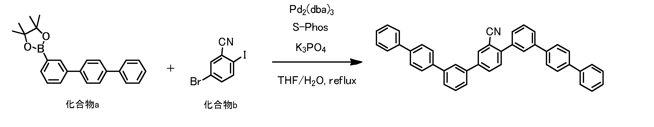
1. Synthesis Example The compound represented by the general formula (1) can be synthesized by combining known reactions.
(Synthesis Example 1)
Synthesis of compound (2-11)
前記一般式(1)で表される化合物は、公知の反応を組み合わせて合成できる。
(合成例1)
化合物(2-11)の合成
(Synthesis Example 1)
Synthesis of compound (2-11)
100ml三つ口フラスコに三りん酸カリウム7.44g、化合物b 0.61g、テトラヒドロフラン20ml、蒸留水10mlを加え、室温にて攪拌させた。次いでS-Phos 0.23g、化合物a 2g、Pd2(dba)3 0.13gを加え、7時間加熱還流させた。反応後、トルエン20mlを加え、沈殿物をろ過し、メタノール洗浄を施した。得られた固体をメタノールに分散させ、1時間加熱還流させた後、ろ過およびメタノール洗浄、乾燥を施し1.34gの灰色固体を得た。これを昇華精製し、化合物(2-11)を得た。得られた化合物は400MHzの1H-NMRにて同定した。
To a 100 ml three-necked flask, 7.44 g of potassium triphosphate, 0.61 g of compound b, 20 ml of tetrahydrofuran and 10 ml of distilled water were added and stirred at room temperature. Next, 0.23 g of S-Phos, 2 g of compound a, and 0.13 g of Pd 2 (dba) 3 were added and heated to reflux for 7 hours. After the reaction, 20 ml of toluene was added, and the precipitate was filtered and washed with methanol. The obtained solid was dispersed in methanol, heated to reflux for 1 hour, filtered, washed with methanol, and dried to obtain 1.34 g of a gray solid. This was purified by sublimation to obtain compound (2-11). The obtained compound was identified by 1 H-NMR at 400 MHz.
化合物(2-11)の1H-NMRスペクトルを図4に記載した。
図4から読み取られる化合物2-11の1H-NMRデータの詳細を下記に示す。 The 1 H-NMR spectrum of the compound (2-11) is shown in FIG.
Details of 1 H-NMR data of Compound 2-11 read from FIG. 4 are shown below.
図4から読み取られる化合物2-11の1H-NMRデータの詳細を下記に示す。 The 1 H-NMR spectrum of the compound (2-11) is shown in FIG.
Details of 1 H-NMR data of Compound 2-11 read from FIG. 4 are shown below.
化合物(2-11)と同様の方法で下記スキームに従って化合物(1-1)、(1-3)、(1-5)、(1-7)、(2-1)、(3-2)、(3-11)、(7-10)、(7-11)、(7-13)、(9-12)、(10-3)、(10-6)を合成した。
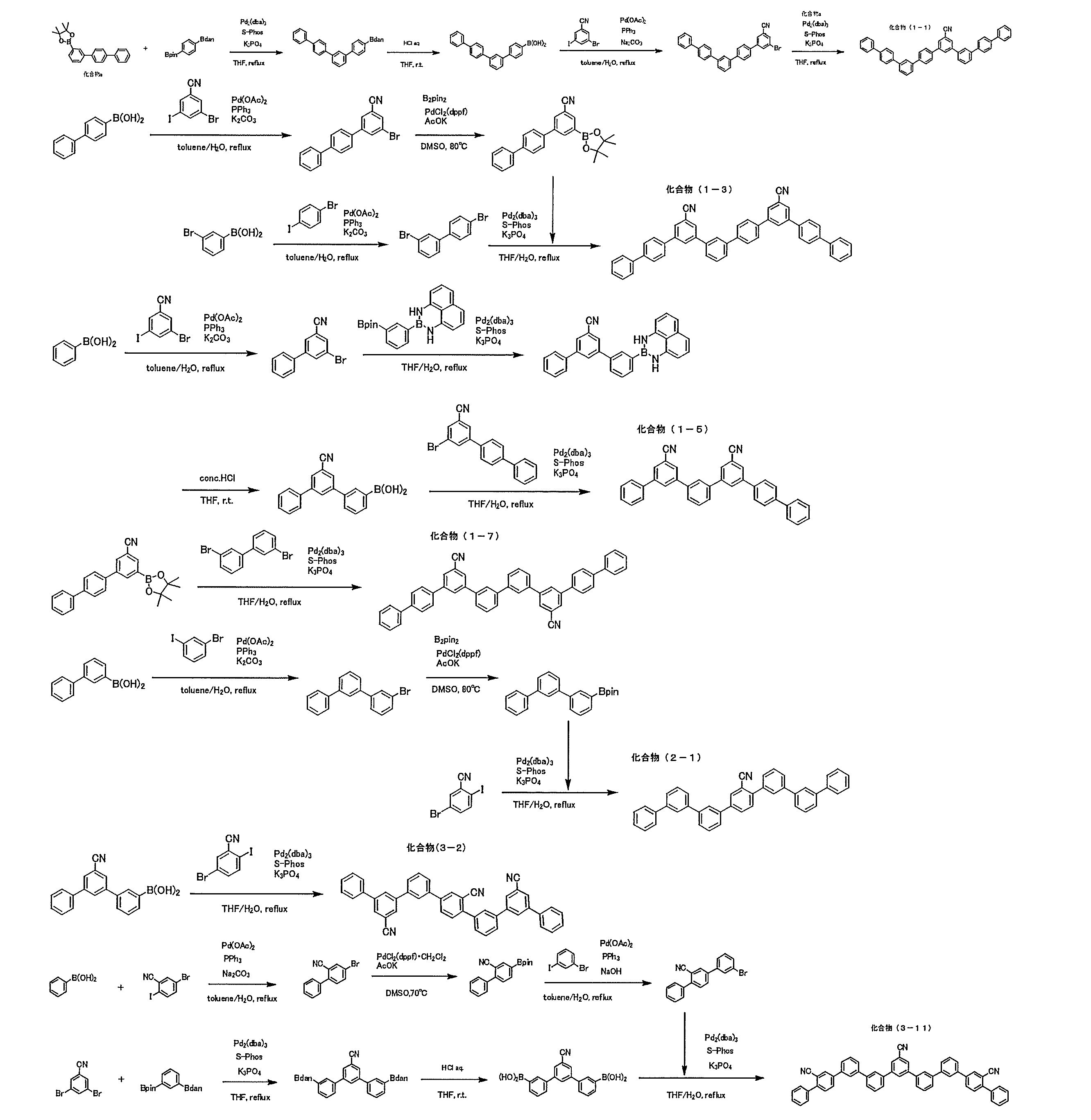
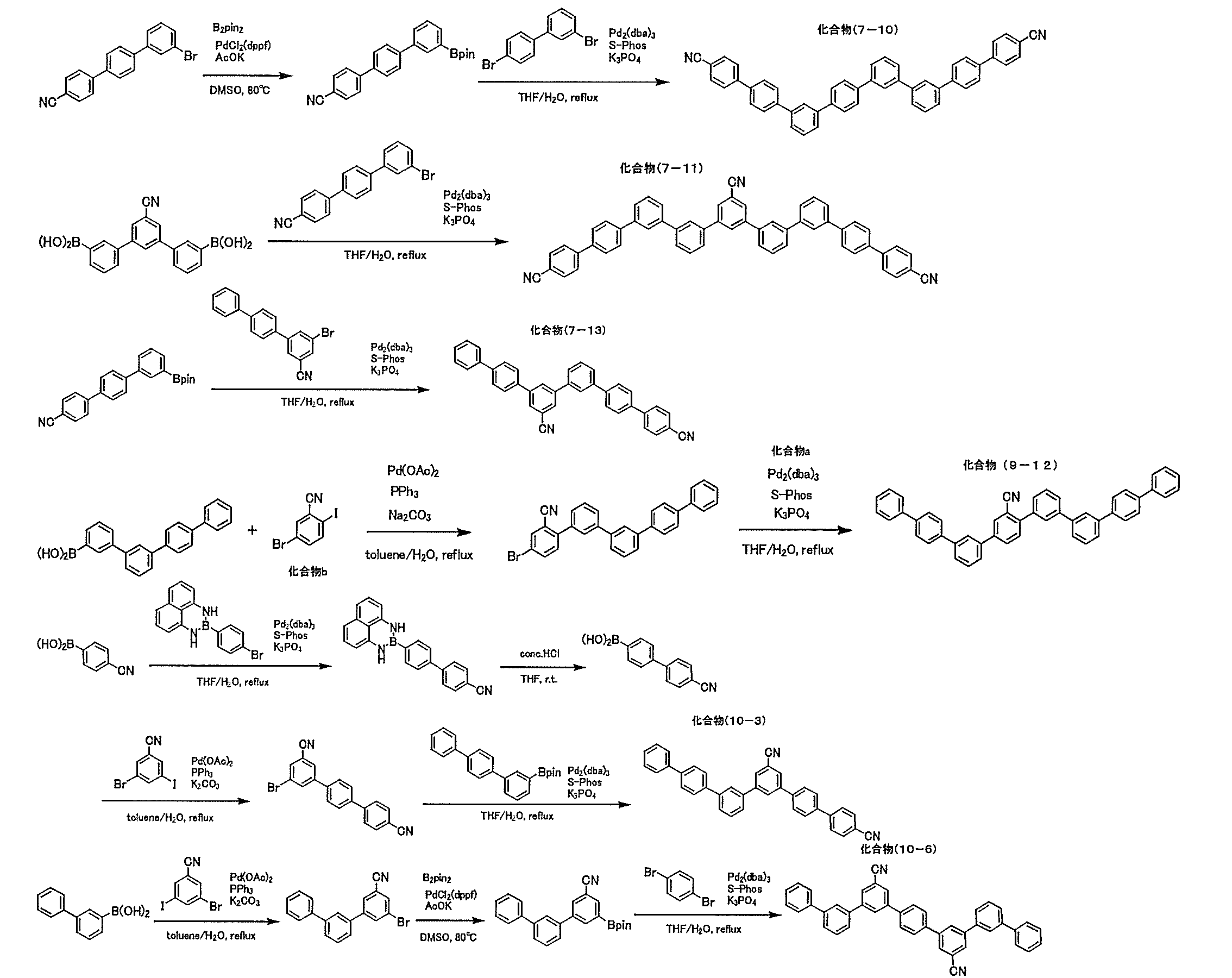
Compounds (1-1), (1-3), (1-5), (1-7), (2-1), (3-2) according to the following scheme in the same manner as for compound (2-11) , (3-11), (7-10), (7-11), (7-13), (9-12), (10-3), and (10-6) were synthesized.
得られた化合物(1-5)の1H-NMRデータの詳細を下記に示す。
化合物(1-5)1H-NMR(CDCl3)[ppm];8.092(1H,s),8.051(1H, s), 7.933(1H, s), 7.903(2H, s), 7.866(1H, s), 7.831(1H, s), 7.76-7.62(11H, m), 7.55-7.44(6H, m) Details of 1 H-NMR data of the obtained compound (1-5) are shown below.
Compound (1-5) 1 H-NMR (CDCl 3 ) [ppm]; 8.092 (1H, s), 8.051 (1H, s), 7.933 (1H, s), 7.903 (2H , s), 7.866 (1H, s), 7.831 (1H, s), 7.76-7.62 (11H, m), 7.55-7.44 (6H, m)
得られた化合物(2-1)の1H-NMRデータの詳細を下記に示す。
1H-NMR(CDCl3)[ppm];8.50(1H,s),8.26(1H, d), 8.19(1H, s), 8.06(2H, s), 8.04(1H, s), 7.94-7.88(9H, m), 7.767(1H, s), 7.73-7.58(7H, m), 7.53-7.47(4H, m), 7.43-7.38(2H, m) Details of 1 H-NMR data of the obtained compound (2-1) are shown below.
1 H-NMR (CDCl 3 ) [ppm]; 8.50 (1H, s), 8.26 (1H, d), 8.19 (1H, s), 8.06 (2H, s), 8. 04 (1H, s), 7.94-7.88 (9H, m), 7.767 (1H, s), 7.73-7.58 (7H, m), 7.53-7.47 ( 4H, m), 7.43-7.38 (2H, m)
化合物(7-13)の1H-NMRスペクトルを図5に記載した。
FIG. 5 shows the 1 H-NMR spectrum of the compound (7-13).
以上のように合成し、実施例で使用した化合物を、同じく実施例で使用した比較化合物と共に、以下に示す。
The compounds synthesized as described above and used in the examples are shown below together with the comparative compounds used in the examples.
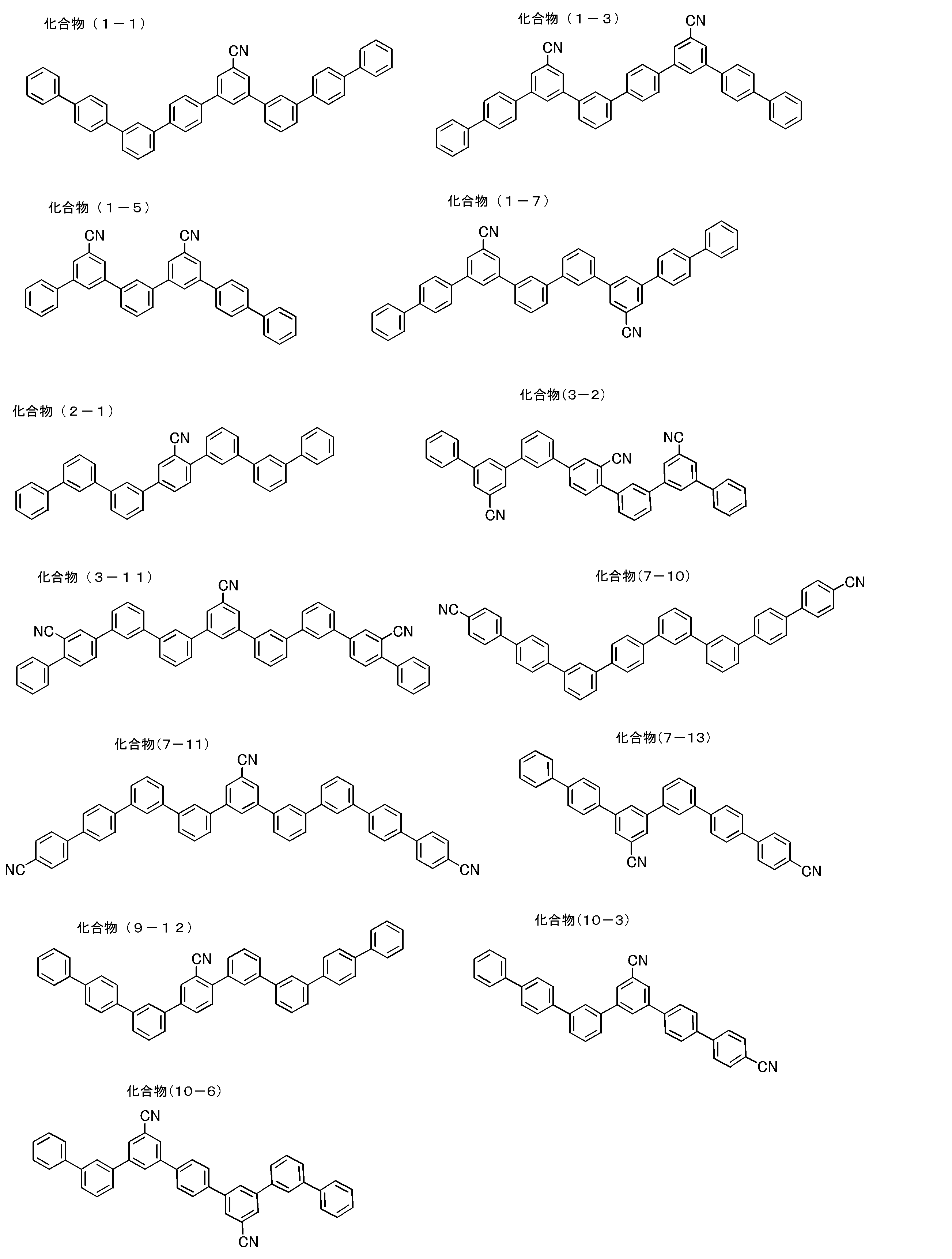
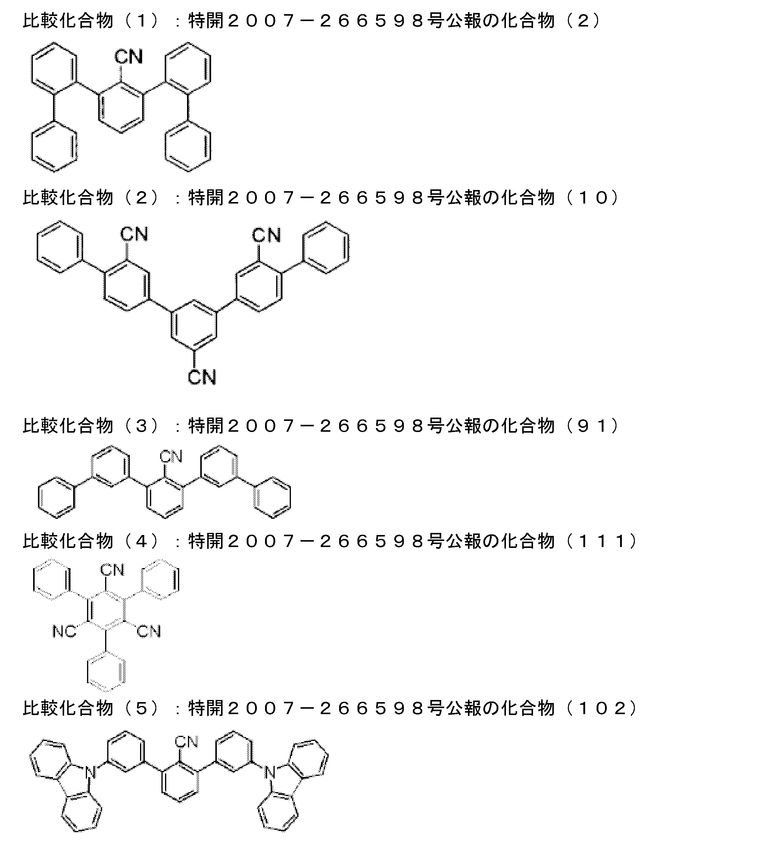
2.素子作製・評価
素子作製に用いた材料は全て昇華精製を行い、高速液体クロマトグラフィー(東ソーTSKgel ODS-100Z)により純度(254nmの吸収強度面積比)が99.1%以上であることを確認した。 2. Element fabrication / evaluation All materials used for element fabrication were purified by sublimation, and it was confirmed by high performance liquid chromatography (Tosoh TSKgel ODS-100Z) that the purity (254 nm absorption intensity area ratio) was 99.1% or more. .
素子作製に用いた材料は全て昇華精製を行い、高速液体クロマトグラフィー(東ソーTSKgel ODS-100Z)により純度(254nmの吸収強度面積比)が99.1%以上であることを確認した。 2. Element fabrication / evaluation All materials used for element fabrication were purified by sublimation, and it was confirmed by high performance liquid chromatography (Tosoh TSKgel ODS-100Z) that the purity (254 nm absorption intensity area ratio) was 99.1% or more. .
(実施例1)
厚み0.5mm、2.5cm角のITO膜を有するガラス基板(ジオマテック社製、表面抵抗10Ω/□)を洗浄容器に入れ、2-プロパノール中で超音波洗浄した後、30分間UV-オゾン処理を行った。この透明陽極(ITO膜)上に真空蒸着法にて以下の有機層を順次蒸着した。
第1層:下記化合物(A) :膜厚10nm
第2層:HTL-1 :膜厚25nm
第3層:化合物(1-1)及びGD-1(質量比90:10) :膜厚40nm
第4層:ETL-1 :膜厚40nm
この上に、フッ化リチウム0.1nm及び金属アルミニウム100nmをこの順に蒸着し陰極とした。
この積層体を、大気に触れさせることなく、窒素ガスで置換したグローブボックス内に入れ、ガラス製の封止缶及び紫外線硬化型の接着剤(XNR5516HV、長瀬チバ(株)製)を用いて封止し、素子1を得た。 Example 1
A glass substrate having a thickness of 0.5 mm and a 2.5 cm square ITO film (manufactured by Geomat Co., Ltd.,surface resistance 10 Ω / □) is placed in a cleaning container, subjected to ultrasonic cleaning in 2-propanol, and then subjected to UV-ozone treatment for 30 minutes. Went. The following organic layers were sequentially deposited on the transparent anode (ITO film) by vacuum deposition.
First layer: Compound (A) below:Film thickness 10 nm
Second layer: HTL-1: film thickness 25 nm
Third layer: Compound (1-1) and GD-1 (mass ratio 90:10):film thickness 40 nm
Fourth layer: ETL-1:film thickness 40 nm
On top of this, 0.1 nm of lithium fluoride and 100 nm of metallic aluminum were vapor-deposited in this order to form a cathode.
This laminated body is put in a glove box substituted with nitrogen gas without being exposed to the atmosphere, and sealed with a glass sealing can and an ultraviolet curable adhesive (XNR5516HV, manufactured by Nagase Ciba Co., Ltd.). Thedevice 1 was obtained.
厚み0.5mm、2.5cm角のITO膜を有するガラス基板(ジオマテック社製、表面抵抗10Ω/□)を洗浄容器に入れ、2-プロパノール中で超音波洗浄した後、30分間UV-オゾン処理を行った。この透明陽極(ITO膜)上に真空蒸着法にて以下の有機層を順次蒸着した。
第1層:下記化合物(A) :膜厚10nm
第2層:HTL-1 :膜厚25nm
第3層:化合物(1-1)及びGD-1(質量比90:10) :膜厚40nm
第4層:ETL-1 :膜厚40nm
この上に、フッ化リチウム0.1nm及び金属アルミニウム100nmをこの順に蒸着し陰極とした。
この積層体を、大気に触れさせることなく、窒素ガスで置換したグローブボックス内に入れ、ガラス製の封止缶及び紫外線硬化型の接着剤(XNR5516HV、長瀬チバ(株)製)を用いて封止し、素子1を得た。 Example 1
A glass substrate having a thickness of 0.5 mm and a 2.5 cm square ITO film (manufactured by Geomat Co., Ltd.,
First layer: Compound (A) below:
Second layer: HTL-1: film thickness 25 nm
Third layer: Compound (1-1) and GD-1 (mass ratio 90:10):
Fourth layer: ETL-1:
On top of this, 0.1 nm of lithium fluoride and 100 nm of metallic aluminum were vapor-deposited in this order to form a cathode.
This laminated body is put in a glove box substituted with nitrogen gas without being exposed to the atmosphere, and sealed with a glass sealing can and an ultraviolet curable adhesive (XNR5516HV, manufactured by Nagase Ciba Co., Ltd.). The
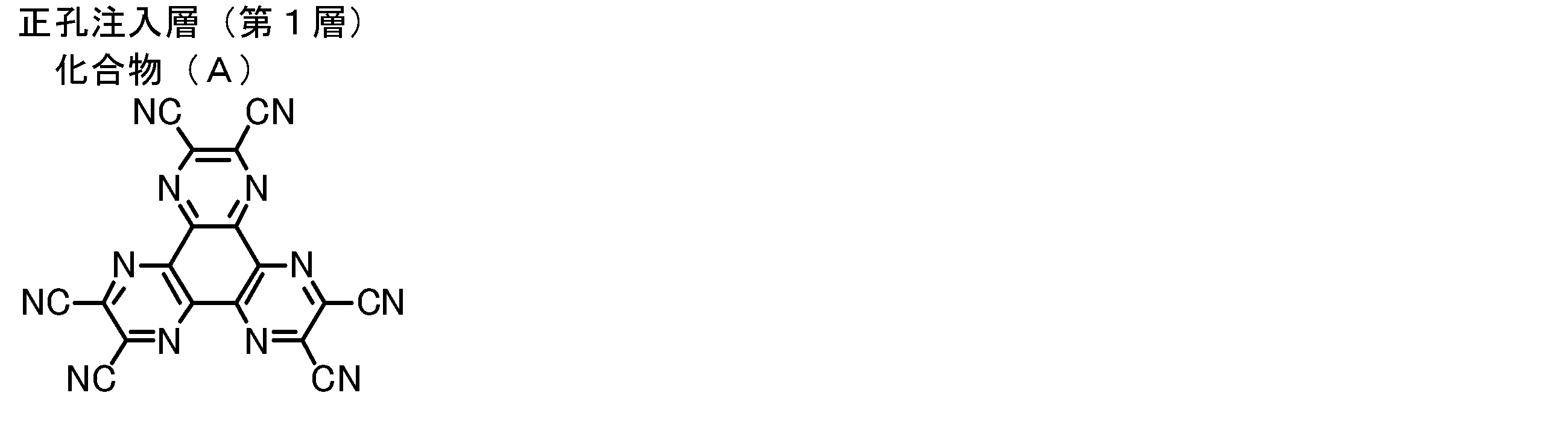
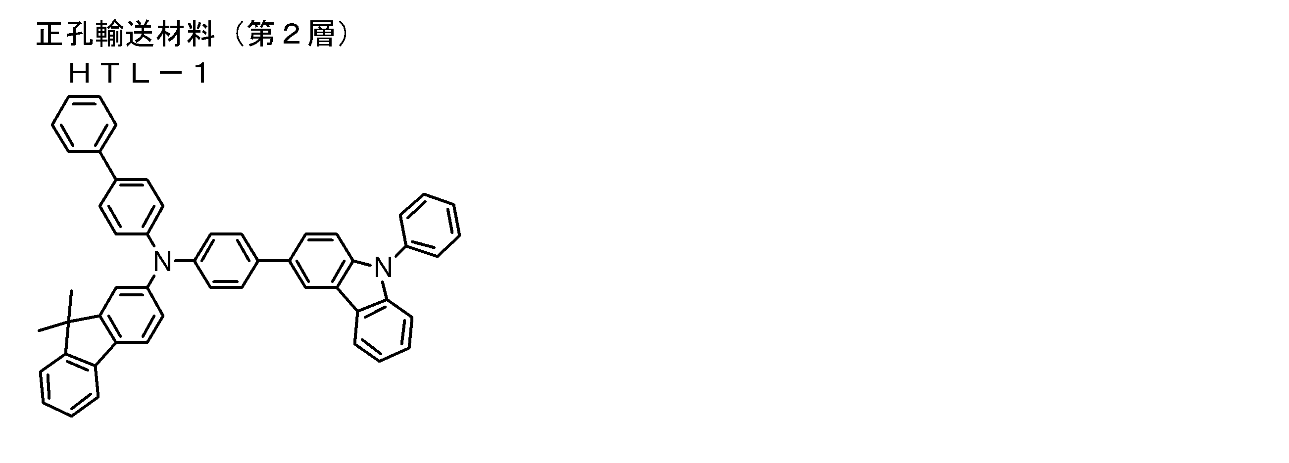
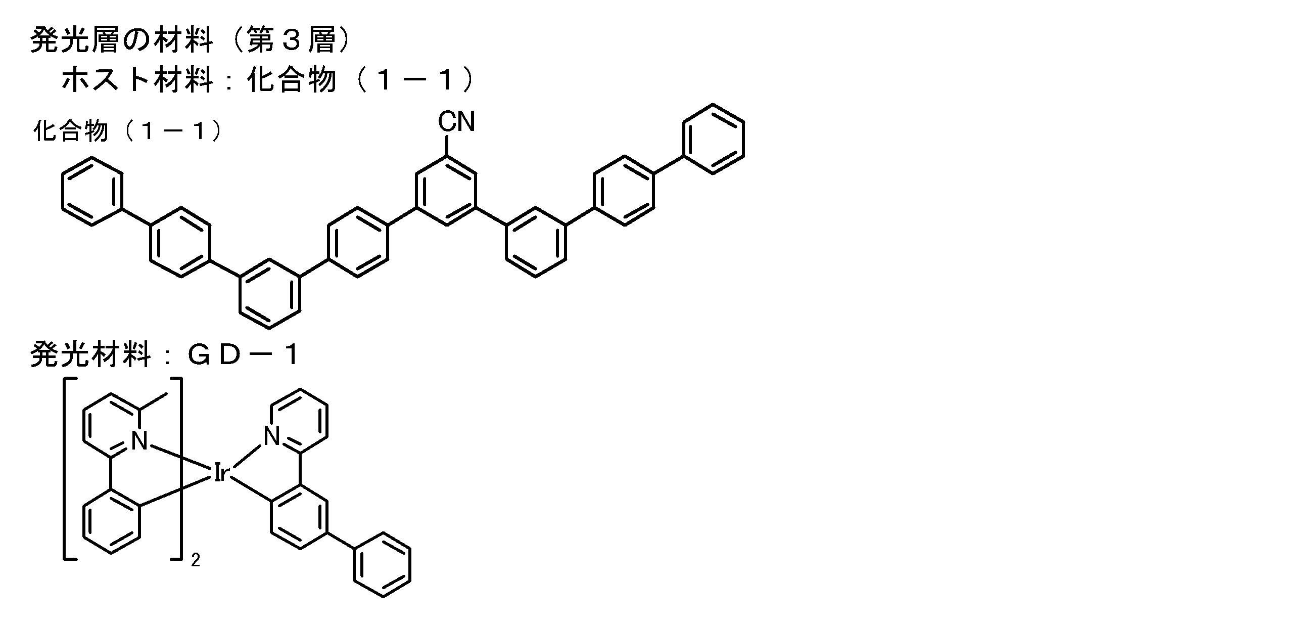
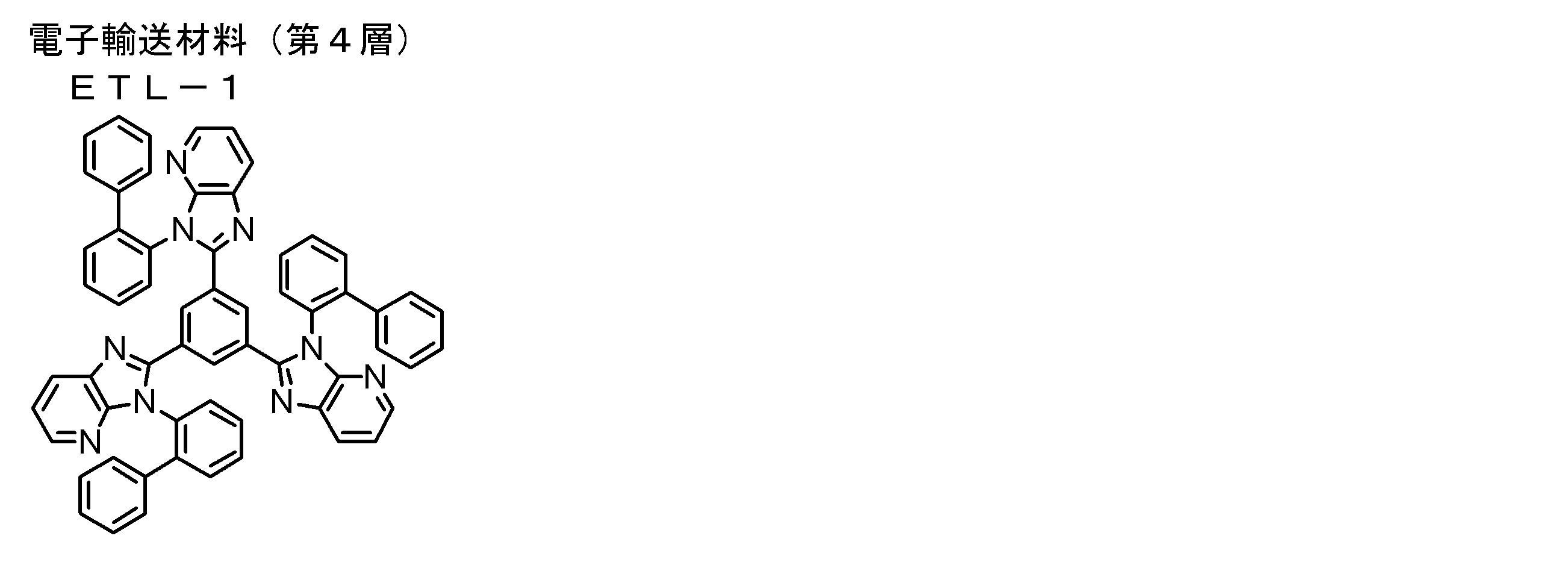
(実施例2~11、比較例1~5)
素子1の調製において、第3層の化合物(1-1)を、下記表1に示す一般式(1)で表される化合物及び上述の比較化合物(1)~比較化合物(5)に置き換える以外は素子1と同様にして、各実施例および比較例の素子を得た。 (Examples 2 to 11, Comparative Examples 1 to 5)
In the preparation of theelement 1, the compound (1-1) in the third layer was replaced with the compound represented by the general formula (1) shown in the following Table 1 and the above-mentioned comparative compounds (1) to (5). In the same manner as in the element 1, elements of the examples and comparative examples were obtained.
素子1の調製において、第3層の化合物(1-1)を、下記表1に示す一般式(1)で表される化合物及び上述の比較化合物(1)~比較化合物(5)に置き換える以外は素子1と同様にして、各実施例および比較例の素子を得た。 (Examples 2 to 11, Comparative Examples 1 to 5)
In the preparation of the
(実施例15~25、比較例6~10)
素子1の調製において、第3層の化合物(1-1)及び第4層のETL-1の両者を、下記表1に示す一般式(1)で表される化合物及び上述の比較化合物(1)~比較化合物(5)に置き換える以外は素子1と同様にして、素子15~25、比較素子6~10を得た。 (Examples 15 to 25, Comparative Examples 6 to 10)
In the preparation of theelement 1, both the compound (1-1) of the third layer and the ETL-1 of the fourth layer were converted into a compound represented by the general formula (1) shown in Table 1 below and the above-mentioned comparative compound (1 To Elements 15 to 25 and Comparative Elements 6 to 10 were obtained in the same manner as Element 1, except that the compound was replaced with Comparative Compound (5).
素子1の調製において、第3層の化合物(1-1)及び第4層のETL-1の両者を、下記表1に示す一般式(1)で表される化合物及び上述の比較化合物(1)~比較化合物(5)に置き換える以外は素子1と同様にして、素子15~25、比較素子6~10を得た。 (Examples 15 to 25, Comparative Examples 6 to 10)
In the preparation of the
これらの素子を以下の方法で、効率、耐久性、駆動電圧の観点で評価した結果を下記表1に示す。
Table 1 below shows the results of evaluating these elements from the viewpoint of efficiency, durability, and driving voltage by the following method.
(駆動電圧)
各素子を輝度が1000cd/m2になるように直流電圧を印加して発光させる。この時の印加電圧を駆動電圧評価の指標とした。駆動電圧が6V未満である場合を◎、6V以上7V未満である場合を○、7V以上8V未満である場合を△、8V以上である場合を×として、下記表1に示した。 (Drive voltage)
Each element is caused to emit light by applying a DC voltage so that the luminance becomes 1000 cd / m 2 . The applied voltage at this time was used as an index for driving voltage evaluation. Table 1 below shows the case where the driving voltage is less than 6V, ◯, the case where it is 6V or more and less than 7V, ◯, the case where it is 7V or more and less than 8V, and the case where it is 8V or more.
(外部量子効率)
東陽テクニカ製ソースメジャーユニット2400を用いて、直流電圧を各素子に印加し発光させ、その輝度をトプコン社製輝度計BM-8を用いて測定した。発光スペクトルと発光ピーク波長は浜松ホトニクス製スペクトルアナライザーPMA-11を用いて測定した。これらを元に輝度が1000cd/m2付近の外部量子効率を輝度換算法により算出した。
外部量子効率が15%以上である場合を◎、10%以上15%未満である場合を○、8%以上10%未満である場合を△、8%未満である場合を×として、下記表1に示した。 (External quantum efficiency)
Using a source measure unit 2400 manufactured by Toyo Technica, a DC voltage was applied to each element to emit light, and the luminance was measured using a luminance meter BM-8 manufactured by Topcon Corporation. The emission spectrum and emission peak wavelength were measured using a spectrum analyzer PMA-11 manufactured by Hamamatsu Photonics. Based on these, the external quantum efficiency with a luminance of around 1000 cd / m 2 was calculated by the luminance conversion method.
Table 1 below shows the case where the external quantum efficiency is 15% or more: ◎: 10% or more and less than 15%; ◯, 8% or more and less than 10%; It was shown to.
(耐久性)
各素子を、室温(20℃)で輝度が5000cd/m2になるように直流電圧を印加して発光させ続け、輝度が4000cd/m2になるまでに要した時間を耐久性の指標とした。700時間以上である場合を◎、500時間以上700時間未満である場合を○、300時間以上500時間未満である場合を△、300時間未満である場合を×として、下記表1に示した。 (durability)
Each element, luminance at room temperature (20 ° C.) to continue applying to emit light a DC voltage to be 5000 cd / m 2, luminance is used as an index of durability time taken until 4000 cd / m 2 . Table 1 below shows ◎ when 700 hours or more, ◯ when 500 hours or more and less than 700 hours, Δ when 300 hours or more and less than 500 hours, and × when less than 300 hours.
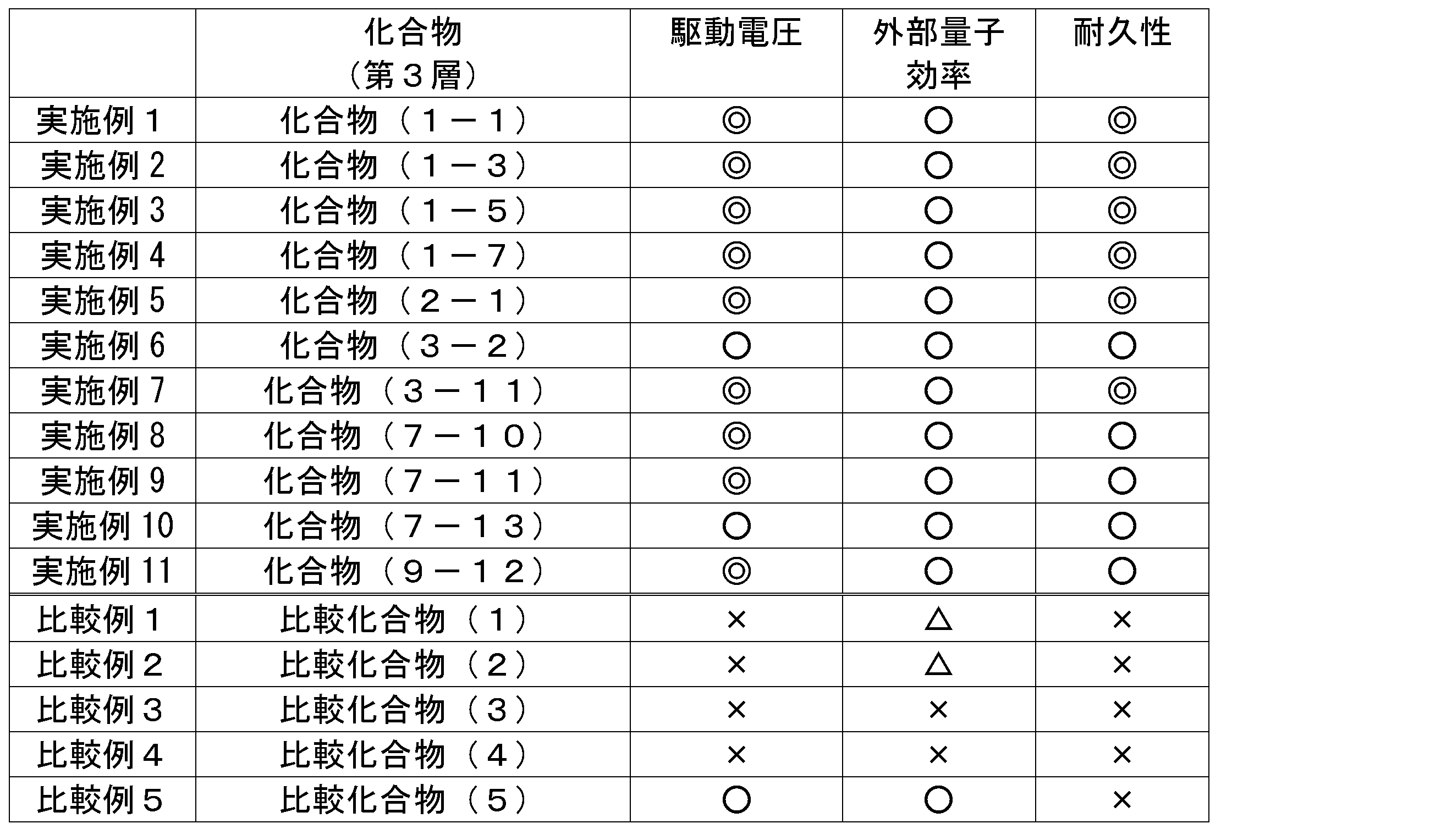
(実施例12~14、比較例6~10)
素子1の調製において、を下記に記載の化合物に置き換えることにより素子9を得た。また、第3層の化合物(1-1)を下記表2に示す一般式(1)で表される化合物及び上述の比較化合物(1)~比較化合物(5)に置き換える以外は素子9と同様にして、各実施例および比較例の素子を得た。
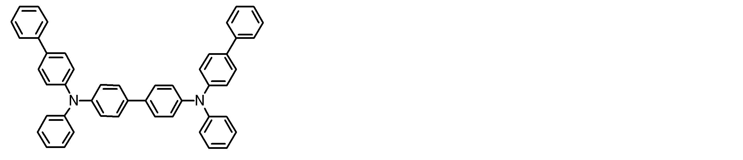
(Examples 12 to 14, Comparative Examples 6 to 10)
In the preparation ofdevice 1, device 9 was obtained by substituting the compounds described below. Further, the third layer compound (1-1) was the same as the device 9 except that the compound represented by the general formula (1) shown in Table 2 below and the above-mentioned comparative compounds (1) to (5) were replaced. Thus, elements of the examples and comparative examples were obtained.
素子1の調製において、を下記に記載の化合物に置き換えることにより素子9を得た。また、第3層の化合物(1-1)を下記表2に示す一般式(1)で表される化合物及び上述の比較化合物(1)~比較化合物(5)に置き換える以外は素子9と同様にして、各実施例および比較例の素子を得た。
In the preparation of
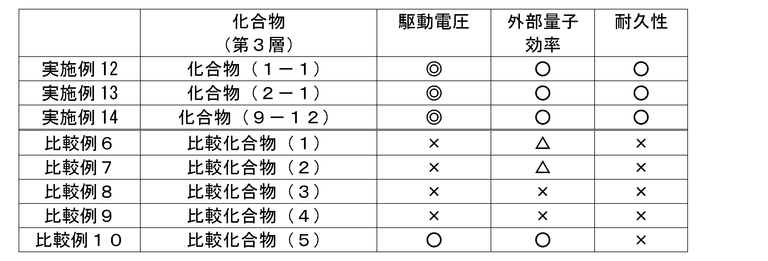
(実施例15~24、比較例11~15)
素子11の調製において、第4層の化合物(ETL-1)を本発明の化合物(1-3)に置き換えることにより素子15を得た。また、第4層の化合物(1-3)を下記表3に示す一般式(1)で表される化合物及び上述の比較化合物(5)に置き換える以外は素子1と同様にして、各実施例および比較例の素子を得た。 (Examples 15 to 24, Comparative Examples 11 to 15)
In the preparation of theelement 11, the element 15 was obtained by replacing the compound (ETL-1) in the fourth layer with the compound (1-3) of the present invention. In addition, each example was performed in the same manner as in the element 1 except that the compound (1-3) in the fourth layer was replaced with the compound represented by the general formula (1) shown in Table 3 below and the above-described comparative compound (5). And the element of the comparative example was obtained.
素子11の調製において、第4層の化合物(ETL-1)を本発明の化合物(1-3)に置き換えることにより素子15を得た。また、第4層の化合物(1-3)を下記表3に示す一般式(1)で表される化合物及び上述の比較化合物(5)に置き換える以外は素子1と同様にして、各実施例および比較例の素子を得た。 (Examples 15 to 24, Comparative Examples 11 to 15)
In the preparation of the
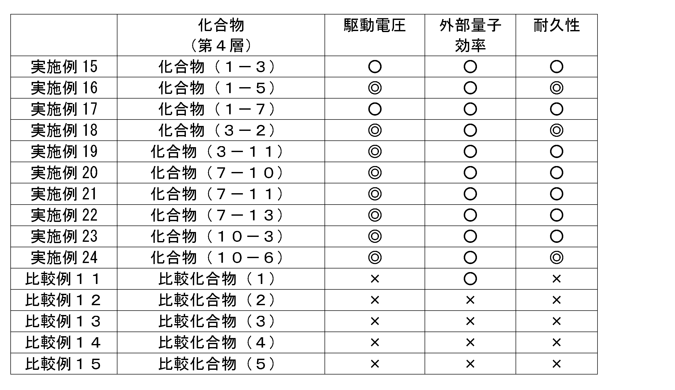
上記表1~表3より、本発明の電荷輸送材料を用いることで、低駆動電圧で、かつ、耐久性に優れた有機電界発光素子が得られることが分かった。
また、本発明の電荷輸送材料を用いた有機電界発光素子は、効率も高い傾向にあることがわかった。
なお、実施例1~24で作製した有機電界発光素子の発光ピーク波長は510~530nmであった。 From Tables 1 to 3, it was found that an organic electroluminescence device having a low driving voltage and excellent durability can be obtained by using the charge transport material of the present invention.
Moreover, it turned out that the organic electroluminescent element using the charge transport material of the present invention tends to have high efficiency.
Note that the emission peak wavelengths of the organic electroluminescent devices prepared in Examples 1 to 24 were 510 to 530 nm.
発光装置、表示装置、照明装置の場合、各画素部で高い電流密度を通じて瞬間的に高輝度発光させる必要があり、本発明の発光素子はそのような場合に発光効率が高くなるように設計されているため、有利に利用することができる。
また、本発明の素子は耐久性にも優れ、発光装置、表示装置、照明装置に好適である。 In the case of a light-emitting device, a display device, and a lighting device, it is necessary to emit light with high brightness instantaneously through a high current density in each pixel portion, and the light-emitting element of the present invention is designed to increase the light emission efficiency in such a case. Therefore, it can be used advantageously.
In addition, the element of the present invention is excellent in durability and is suitable for a light emitting device, a display device, and a lighting device.
2・・・基板
3・・・陽極
4・・・正孔注入層
5・・・正孔輸送層
6・・・発光層
7・・・正孔ブロック層
8・・・電子輸送層
9・・・陰極
10・・・有機電界発光素子(有機EL素子)
11・・・有機層
12・・・保護層
14・・・接着層
16・・・封止容器
20・・・発光装置
30・・・光散乱部材
30A・・・光入射面
30B・・・光出射面
31・・・透明基板
32・・・微粒子
40・・・照明装置 DESCRIPTION OFSYMBOLS 2 ... Substrate 3 ... Anode 4 ... Hole injection layer 5 ... Hole transport layer 6 ... Light emitting layer 7 ... Hole block layer 8 ... Electron transport layer 9 ...・ Cathode 10: Organic electroluminescent device (organic EL device)
DESCRIPTION OFSYMBOLS 11 ... Organic layer 12 ... Protective layer 14 ... Adhesive layer 16 ... Sealing container 20 ... Light-emitting device 30 ... Light scattering member 30A ... Light incident surface 30B ... Light Output surface 31 ... Transparent substrate 32 ... Fine particle 40 ... Illumination device
3・・・陽極
4・・・正孔注入層
5・・・正孔輸送層
6・・・発光層
7・・・正孔ブロック層
8・・・電子輸送層
9・・・陰極
10・・・有機電界発光素子(有機EL素子)
11・・・有機層
12・・・保護層
14・・・接着層
16・・・封止容器
20・・・発光装置
30・・・光散乱部材
30A・・・光入射面
30B・・・光出射面
31・・・透明基板
32・・・微粒子
40・・・照明装置 DESCRIPTION OF
DESCRIPTION OF
Claims (15)
- 下記一般式(1)で表される構造であり、かつ、6~19個の単環のベンゼン環を含む化合物からなる電荷輸送材料。
一般式(1)

General formula (1)
- 前記一般式(1)におけるR111~R128のうち、1または2個がシアノ基であることを特徴とする請求項1に記載の電荷輸送材料。 2. The charge transport material according to claim 1, wherein one or two of R 111 to R 128 in the general formula (1) are cyano groups.
- 前記一般式(1)で表される構造を有する化合物の分子量が500~1000であることを特徴とする請求項1または2に記載の電荷輸送材料。 3. The charge transport material according to claim 1, wherein the compound having the structure represented by the general formula (1) has a molecular weight of 500 to 1,000.
- 基板と、
該基板上に配置され、陽極及び陰極を含む一対の電極と、
該電極間に配置された有機層とを有し、
前記有機層が、燐光発光材料請求項1~3のいずれか一項に記載の電荷輸送材料を含有することを特徴とする有機電界発光素子。 A substrate,
A pair of electrodes disposed on the substrate, including an anode and a cathode;
An organic layer disposed between the electrodes,
An organic electroluminescent device, wherein the organic layer contains a phosphorescent material and the charge transport material according to any one of claims 1 to 3. - 前記有機層が、前記燐光発光材料を含む発光層を有し、該発光層が前記一般式(1)で表される構造の化合物を含有することを特徴とする請求項4に記載の有機電界発光素子。 5. The organic electric field according to claim 4, wherein the organic layer has a light emitting layer containing the phosphorescent light emitting material, and the light emitting layer contains a compound having a structure represented by the general formula (1). Light emitting element.
- 前記発光層が、前記一般式(1)で表される構造の化合物として、下記一般式(3-A)で表される部分構造で表される部分構造を含むことを特徴とする請求項5に記載の有機電界発光素子。
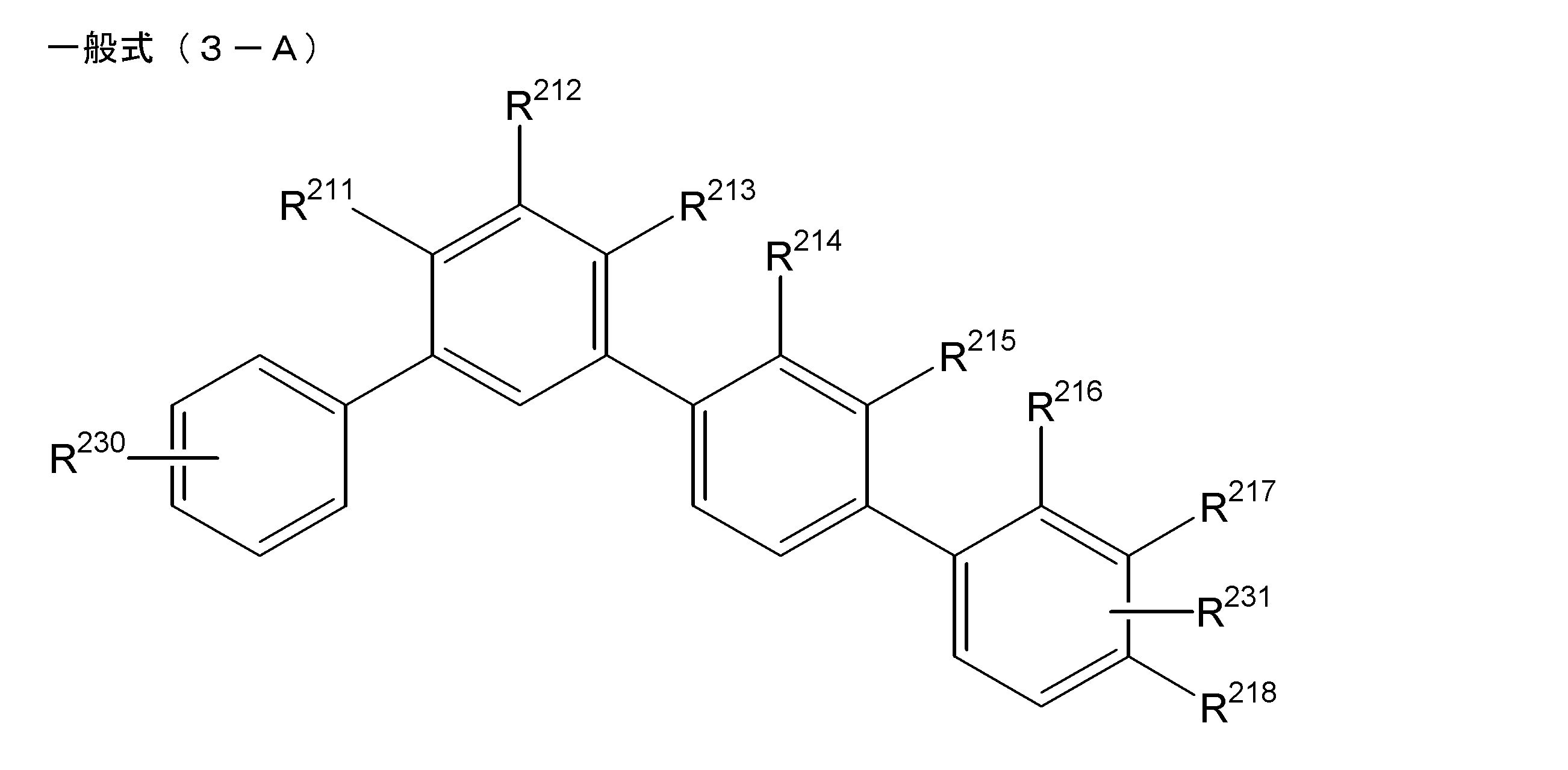
- 前記発光層が、前記一般式(1)で表される構造の化合物として、下記部分構造群(1A)で表される部分構造を有する化合物を含有することを特徴とする請求項5または6に記載の有機電界発光素子。
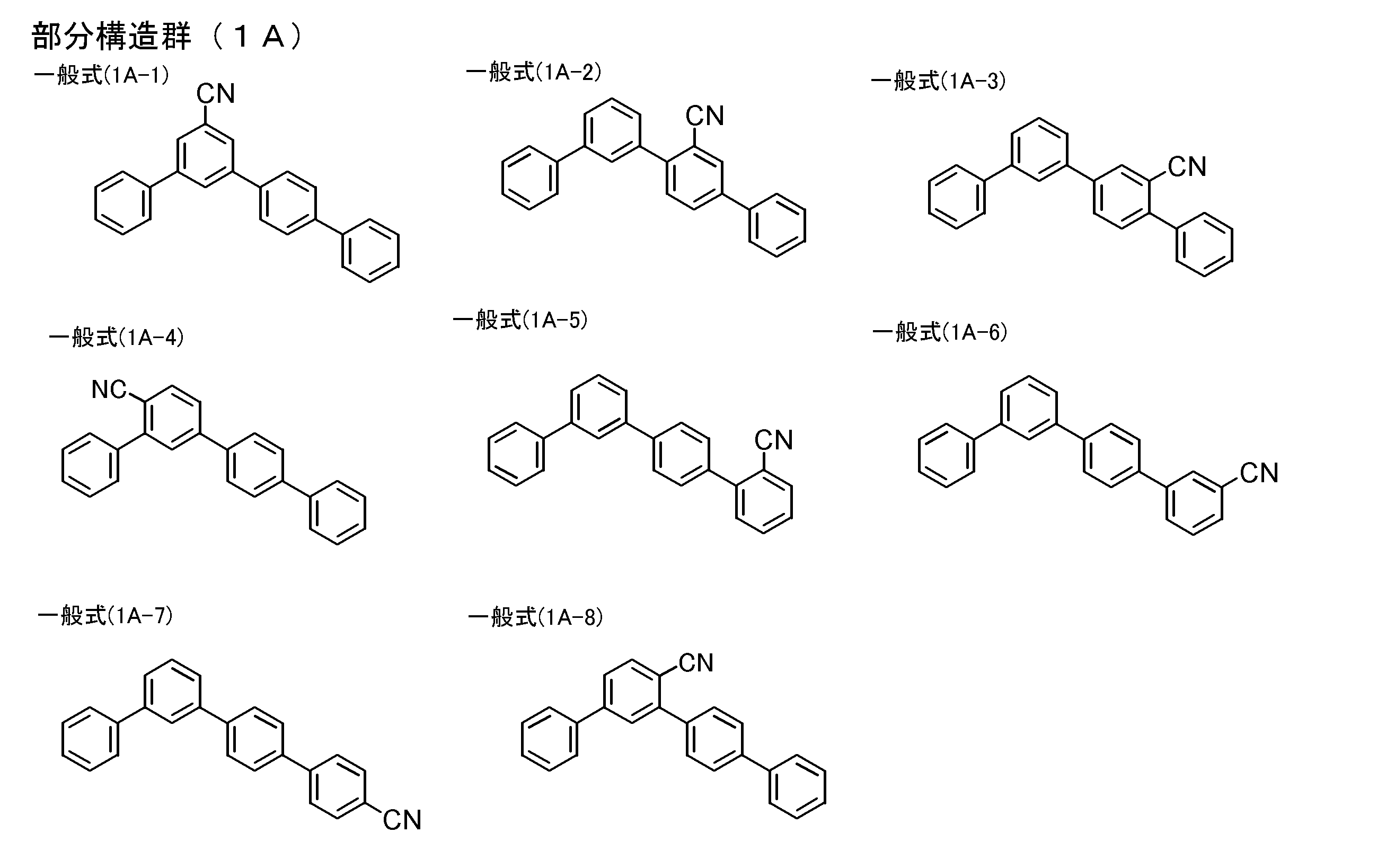
- 前記有機層が、前記燐光発光材料を含む発光層とその他の有機層を有し、
前記発光層と前記陰極との間に配置されたその他の有機層が、前記一般式(1)で表される構造の化合物を含有することを特徴とする請求項5~7のいずれか一項に記載の有機電界発光素子。 The organic layer has a light emitting layer containing the phosphorescent material and other organic layers,
The other organic layer disposed between the light emitting layer and the cathode contains a compound having a structure represented by the general formula (1). The organic electroluminescent element of description. - 前記発光層と前記陰極との間に配置されたその他の有機層が、前記一般式(1)で表される構造の化合物として、下記部分構造群(1A)で表される部分構造を有する化合物を含有することを特徴とする請求項8に記載の有機電界発光素子。
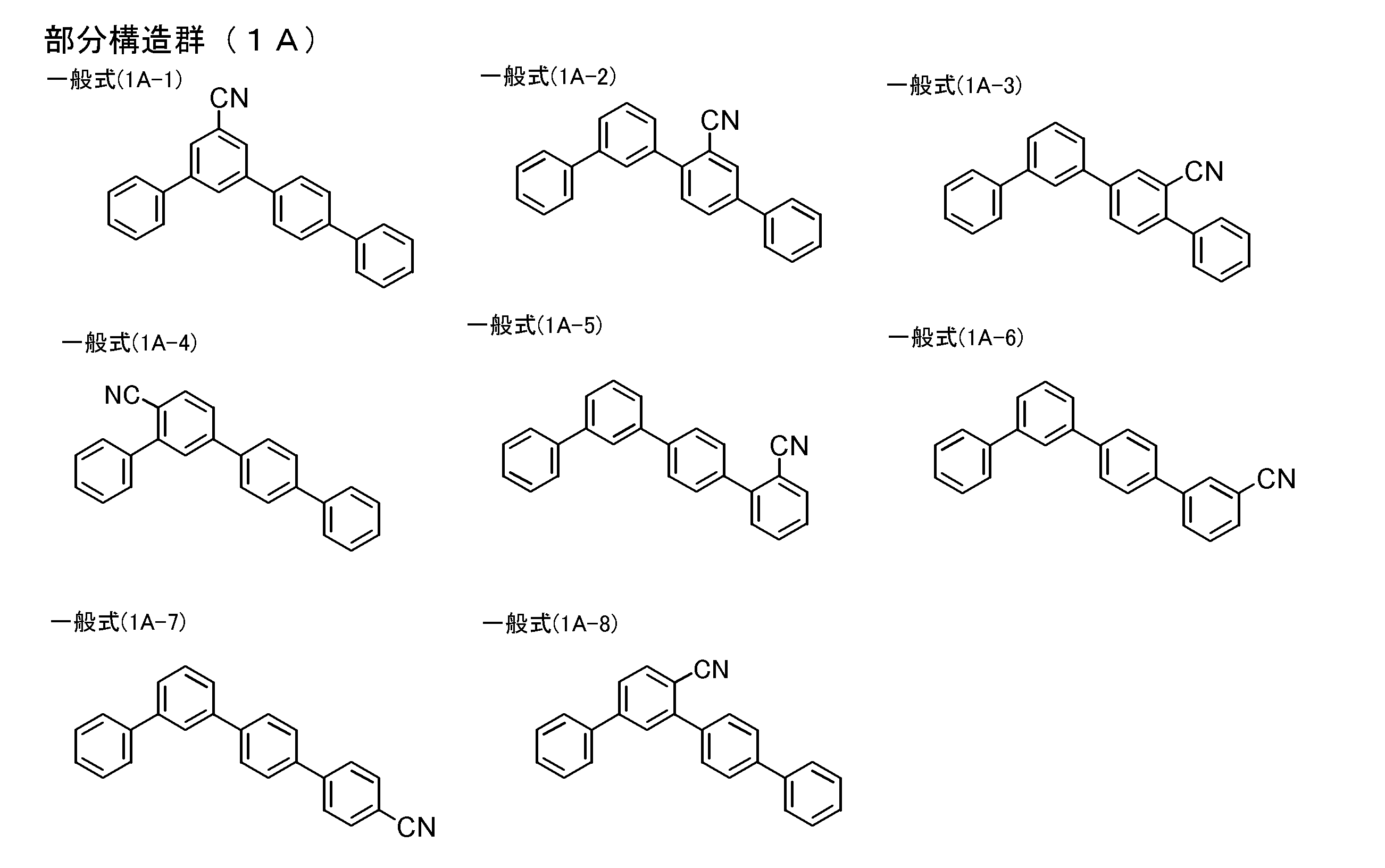
- 前記部分構造群(1A)で表される部分構造を有する化合物において、1つのベンゼン環に3つ以上のベンゼン環が置換されていない鎖状構造であることを特徴とする請求項9に記載の有機電界発光素子。 The compound having a partial structure represented by the partial structure group (1A) is a chain structure in which one or more benzene rings are not substituted on one benzene ring. Organic electroluminescent device.
- 前記一般式(1)で表される構造の化合物として、部分構造群(1A-1)、(1A-2)、(1A-3)、(1A-7)のいずれかで表される部分構造を有する化合物を含有することを特徴とする請求項9または10に記載の有機電界発光素子。 As the compound having the structure represented by the general formula (1), the partial structure represented by any one of the partial structure groups (1A-1), (1A-2), (1A-3), and (1A-7) The organic electroluminescent element according to claim 9 or 10, wherein the organic electroluminescent element comprises a compound having the following.
- 前記発光層に前記一般式(1)で表される化合物を少なくとも一種含有し、かつ、
前記発光層と陰極との間に配置されたその他の有機層に前記一般式(1)で表される化合物を少なくとも一種含有することを特徴とする請求項11に記載の有機電界発光素子。 Containing at least one compound represented by the general formula (1) in the light emitting layer, and
The organic electroluminescent element according to claim 11, wherein the other organic layer arranged between the light emitting layer and the cathode contains at least one compound represented by the general formula (1). - 前記発光層に、前記燐光発光材料としてイリジウム(Ir)錯体を用いることを特徴とする請求項8~12のいずれか一項に記載の有機電界発光素子。 13. The organic electroluminescent element according to claim 8, wherein an iridium (Ir) complex is used as the phosphorescent material in the light emitting layer.
- 前記発光層に、前記燐光発光材料として下記一般式(E-1)で表されるイリジウム(Ir)錯体を用いることを特徴とする請求項8~12のいずれか一項に記載の有機電界発光素子。
一般式(E-1)
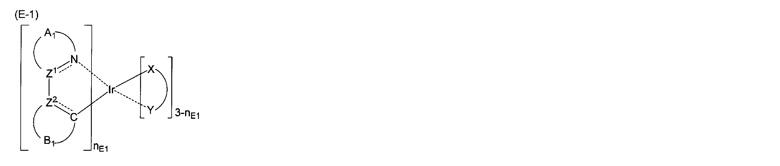
Formula (E-1)
- 請求項8~14のいずれか一項に記載の有機電界発光素子を含むことを特徴とする発光装置、表示装置または照明装置。 A light-emitting device, display device, or illumination device comprising the organic electroluminescent element according to any one of claims 8 to 14.
Applications Claiming Priority (4)
| Application Number | Priority Date | Filing Date | Title |
|---|---|---|---|
| JP2011080214 | 2011-03-31 | ||
| JP2011-080214 | 2011-03-31 | ||
| JP2012072479A JP5906114B2 (en) | 2011-03-31 | 2012-03-27 | Charge transport material, organic electroluminescent element, light emitting device, display device and lighting device |
| JP2012-072479 | 2012-03-27 |
Publications (1)
| Publication Number | Publication Date |
|---|---|
| WO2012133649A1 true WO2012133649A1 (en) | 2012-10-04 |
Family
ID=46931351
Family Applications (1)
| Application Number | Title | Priority Date | Filing Date |
|---|---|---|---|
| PCT/JP2012/058355 WO2012133649A1 (en) | 2011-03-31 | 2012-03-29 | Charge transport material, organic electroluminescence element, light-emitting device, display apparatus, and illumination apparatus |
Country Status (2)
| Country | Link |
|---|---|
| JP (1) | JP5906114B2 (en) |
| WO (1) | WO2012133649A1 (en) |
Cited By (63)
| Publication number | Priority date | Publication date | Assignee | Title |
|---|---|---|---|---|
| EP3056504A1 (en) | 2015-02-16 | 2016-08-17 | Universal Display Corporation | Organic electroluminescent materials and devices |
| EP3061763A1 (en) | 2015-02-27 | 2016-08-31 | Universal Display Corporation | Organic electroluminescent materials and devices |
| EP3098229A1 (en) | 2015-05-15 | 2016-11-30 | Universal Display Corporation | Organic electroluminescent materials and devices |
| EP3101021A1 (en) | 2015-06-01 | 2016-12-07 | Universal Display Corporation | Organic electroluminescent materials and devices |
| EP3124488A1 (en) | 2015-07-29 | 2017-02-01 | Universal Display Corporation | Organic electroluminescent materials and devices |
| EP3159350A1 (en) | 2015-09-03 | 2017-04-26 | Universal Display Corporation | Organic electroluminescent materials and devices |
| EP3205658A1 (en) | 2016-02-09 | 2017-08-16 | Universal Display Corporation | Organic electroluminescent materials and devices |
| EP3231809A2 (en) | 2016-04-11 | 2017-10-18 | Universal Display Corporation | Organic electroluminescent materials and devices |
| EP3261146A2 (en) | 2016-06-20 | 2017-12-27 | Universal Display Corporation | Organic electroluminescent materials and devices |
| EP3261147A1 (en) | 2016-06-20 | 2017-12-27 | Universal Display Corporation | Organic electroluminescent materials and devices |
| EP3270435A2 (en) | 2016-06-20 | 2018-01-17 | Universal Display Corporation | Organic electroluminescent materials and devices |
| EP3297051A1 (en) | 2016-09-14 | 2018-03-21 | Universal Display Corporation | Organic electroluminescent materials and devices |
| EP3301088A1 (en) | 2016-10-03 | 2018-04-04 | Universal Display Corporation | Condensed pyridines as organic electroluminescent materials and devices |
| EP3305796A1 (en) | 2016-10-07 | 2018-04-11 | Universal Display Corporation | Organic electroluminescent materials and devices |
| EP3321258A1 (en) | 2016-11-09 | 2018-05-16 | Universal Display Corporation | 4-phenylbenzo[g]quinazoline or 4-(3,5-dimethylphenylbenzo[g]quinazoline iridium complexes for use as near-infrared or infrared emitting materials in oleds |
| EP3323822A1 (en) | 2016-09-23 | 2018-05-23 | Universal Display Corporation | Organic electroluminescent materials and devices |
| EP3345914A1 (en) | 2017-01-09 | 2018-07-11 | Universal Display Corporation | Organic electroluminescent materials and devices |
| EP3354654A2 (en) | 2016-11-11 | 2018-08-01 | Universal Display Corporation | Organic electroluminescent materials and devices |
| EP3381927A1 (en) | 2017-03-29 | 2018-10-03 | Universal Display Corporation | Organic electroluminescent materials and devices |
| EP3401318A1 (en) | 2017-05-11 | 2018-11-14 | Universal Display Corporation | Organic electroluminescent materials and devices |
| EP3418286A1 (en) | 2017-06-23 | 2018-12-26 | Universal Display Corporation | Organic electroluminescent materials and devices |
| EP3444258A2 (en) | 2017-08-10 | 2019-02-20 | Universal Display Corporation | Organic electroluminescent materials and devices |
| EP3489243A1 (en) | 2017-11-28 | 2019-05-29 | University of Southern California | Carbene compounds and organic electroluminescent devices |
| EP3492480A2 (en) | 2017-11-29 | 2019-06-05 | Universal Display Corporation | Organic electroluminescent materials and devices |
| EP3492528A1 (en) | 2017-11-30 | 2019-06-05 | Universal Display Corporation | Organic electroluminescent materials and devices |
| EP3613751A1 (en) | 2018-08-22 | 2020-02-26 | Universal Display Corporation | Organic electroluminescent materials and devices |
| EP3689889A1 (en) | 2019-02-01 | 2020-08-05 | Universal Display Corporation | Organic electroluminescent materials and devices |
| EP3690973A1 (en) | 2019-01-30 | 2020-08-05 | University Of Southern California | Organic electroluminescent materials and devices |
| EP3709376A1 (en) | 2019-03-12 | 2020-09-16 | Universal Display Corporation | Oled with triplet emitter and excited state lifetime less than 200 ns |
| EP3715353A1 (en) | 2019-03-26 | 2020-09-30 | Universal Display Corporation | Organic electroluminescent materials and devices |
| EP3750897A1 (en) | 2019-06-10 | 2020-12-16 | Universal Display Corporation | Organic electroluminescent materials and devices |
| EP3771717A1 (en) | 2019-07-30 | 2021-02-03 | Universal Display Corporation | Organic electroluminescent materials and devices |
| EP3778614A1 (en) | 2019-08-16 | 2021-02-17 | Universal Display Corporation | Organic electroluminescent materials and devices |
| EP3816175A1 (en) | 2019-11-04 | 2021-05-05 | Universal Display Corporation | Organic electroluminescent materials and devices |
| EP3823055A1 (en) | 2019-11-14 | 2021-05-19 | Universal Display Corporation | Organic electroluminescent materials and devices |
| EP3845545A1 (en) | 2020-01-06 | 2021-07-07 | Universal Display Corporation | Organic electroluminescent materials and devices |
| EP3858945A1 (en) | 2020-01-28 | 2021-08-04 | Universal Display Corporation | Organic electroluminescent materials and devices |
| EP3937268A1 (en) | 2020-07-10 | 2022-01-12 | Universal Display Corporation | Plasmonic oleds and vertical dipole emitters |
| EP4001287A1 (en) | 2020-11-24 | 2022-05-25 | Universal Display Corporation | Organic electroluminescent materials and devices |
| EP4001286A1 (en) | 2020-11-24 | 2022-05-25 | Universal Display Corporation | Organic electroluminescent materials and devices |
| EP4016659A1 (en) | 2020-11-16 | 2022-06-22 | Universal Display Corporation | Organic electroluminescent materials and devices |
| EP4019526A1 (en) | 2018-01-26 | 2022-06-29 | Universal Display Corporation | Organic electroluminescent materials and devices |
| EP4039692A1 (en) | 2021-02-03 | 2022-08-10 | Universal Display Corporation | Organic electroluminescent materials and devices |
| EP4053137A1 (en) | 2021-03-05 | 2022-09-07 | Universal Display Corporation | Organic electroluminescent materials and devices |
| EP4056578A1 (en) | 2021-03-12 | 2022-09-14 | Universal Display Corporation | Organic electroluminescent materials and devices |
| EP4059941A1 (en) | 2021-03-15 | 2022-09-21 | Universal Display Corporation | Organic electroluminescent materials and devices |
| EP4059915A2 (en) | 2021-02-26 | 2022-09-21 | Universal Display Corporation | Organic electroluminescent materials and devices |
| EP4060758A2 (en) | 2021-02-26 | 2022-09-21 | Universal Display Corporation | Organic electroluminescent materials and devices |
| EP4075531A1 (en) | 2021-04-13 | 2022-10-19 | Universal Display Corporation | Plasmonic oleds and vertical dipole emitters |
| EP4074723A1 (en) | 2021-04-05 | 2022-10-19 | Universal Display Corporation | Organic electroluminescent materials and devices |
| EP4075530A1 (en) | 2021-04-14 | 2022-10-19 | Universal Display Corporation | Organic electroluminescent materials and devices |
| EP4079743A1 (en) | 2021-04-23 | 2022-10-26 | Universal Display Corporation | Organic electroluminescent materials and devices |
| EP4086266A1 (en) | 2021-04-23 | 2022-11-09 | Universal Display Corporation | Organic electroluminescent materials and devices |
| EP4112701A2 (en) | 2021-06-08 | 2023-01-04 | University of Southern California | Molecular alignment of homoleptic iridium phosphors |
| EP4151699A1 (en) | 2021-09-17 | 2023-03-22 | Universal Display Corporation | Organic electroluminescent materials and devices |
| EP4185086A1 (en) | 2017-07-26 | 2023-05-24 | Universal Display Corporation | Organic electroluminescent materials and devices |
| EP4212539A1 (en) | 2021-12-16 | 2023-07-19 | Universal Display Corporation | Organic electroluminescent materials and devices |
| EP4242285A1 (en) | 2022-03-09 | 2023-09-13 | Universal Display Corporation | Organic electroluminescent materials and devices |
| EP4265626A2 (en) | 2022-04-18 | 2023-10-25 | Universal Display Corporation | Organic electroluminescent materials and devices |
| EP4282863A1 (en) | 2022-05-24 | 2023-11-29 | Universal Display Corporation | Organic electroluminescent materials and devices |
| EP4293001A1 (en) | 2022-06-08 | 2023-12-20 | Universal Display Corporation | Organic electroluminescent materials and devices |
| EP4299693A1 (en) | 2022-06-28 | 2024-01-03 | Universal Display Corporation | Organic electroluminescent materials and devices |
| EP4326030A1 (en) | 2022-08-17 | 2024-02-21 | Universal Display Corporation | Organic electroluminescent materials and devices |
Families Citing this family (1)
| Publication number | Priority date | Publication date | Assignee | Title |
|---|---|---|---|---|
| KR20230134615A (en) | 2014-07-07 | 2023-09-21 | 미쯔비시 케미컬 주식회사 | Carbon material, method for producing carbon material, and non-aqueous secondary battery using carbon material |
Citations (3)
| Publication number | Priority date | Publication date | Assignee | Title |
|---|---|---|---|---|
| KR20110049554A (en) * | 2009-11-05 | 2011-05-12 | 엘지디스플레이 주식회사 | Blue color fluorescence compounds and organic light emitting diode comprising thereof |
| WO2012014696A1 (en) * | 2010-07-29 | 2012-02-02 | 富士フイルム株式会社 | ORGANIC ELECTROLUMINESCENT ELEMENT AND COMPOUND HAVING p-DICYANOBENZENE STRUCTURE |
| WO2012015017A1 (en) * | 2010-07-30 | 2012-02-02 | 富士フイルム株式会社 | Organic electroluminescent element and organic-electroluminescent-element material that has a dibenzothiophene or dibenzofuran structure |
-
2012
- 2012-03-27 JP JP2012072479A patent/JP5906114B2/en active Active
- 2012-03-29 WO PCT/JP2012/058355 patent/WO2012133649A1/en active Application Filing
Patent Citations (3)
| Publication number | Priority date | Publication date | Assignee | Title |
|---|---|---|---|---|
| KR20110049554A (en) * | 2009-11-05 | 2011-05-12 | 엘지디스플레이 주식회사 | Blue color fluorescence compounds and organic light emitting diode comprising thereof |
| WO2012014696A1 (en) * | 2010-07-29 | 2012-02-02 | 富士フイルム株式会社 | ORGANIC ELECTROLUMINESCENT ELEMENT AND COMPOUND HAVING p-DICYANOBENZENE STRUCTURE |
| WO2012015017A1 (en) * | 2010-07-30 | 2012-02-02 | 富士フイルム株式会社 | Organic electroluminescent element and organic-electroluminescent-element material that has a dibenzothiophene or dibenzofuran structure |
Non-Patent Citations (2)
| Title |
|---|
| DIPTESH SIL ET AL.: "An efficient cotrolled synthesis of bent-core oligoarenes and heteroarenes through ring transformation of 2H-Pyran", TETRAHEDRON LETTERS, vol. 44, 2003, pages 3363 - 3365, XP004417087, DOI: doi:10.1016/S0040-4039(03)00575-6 * |
| JIANPING LU ET AL.: "Pure Deep Blue Light- Emitting Diodes from Alternating Fluonene/ Carbazole Copolymers by Using Suitable Hole- Blocking Materials", MACROMOLECULES, vol. 37, 2004, pages 2442 - 2449 * |
Cited By (87)
| Publication number | Priority date | Publication date | Assignee | Title |
|---|---|---|---|---|
| EP3056504A1 (en) | 2015-02-16 | 2016-08-17 | Universal Display Corporation | Organic electroluminescent materials and devices |
| EP3061763A1 (en) | 2015-02-27 | 2016-08-31 | Universal Display Corporation | Organic electroluminescent materials and devices |
| EP3098229A1 (en) | 2015-05-15 | 2016-11-30 | Universal Display Corporation | Organic electroluminescent materials and devices |
| EP3101021A1 (en) | 2015-06-01 | 2016-12-07 | Universal Display Corporation | Organic electroluminescent materials and devices |
| EP3124488A1 (en) | 2015-07-29 | 2017-02-01 | Universal Display Corporation | Organic electroluminescent materials and devices |
| EP3760635A1 (en) | 2015-09-03 | 2021-01-06 | Universal Display Corporation | Organic electroluminescent materials and devices |
| EP3159350A1 (en) | 2015-09-03 | 2017-04-26 | Universal Display Corporation | Organic electroluminescent materials and devices |
| EP3205658A1 (en) | 2016-02-09 | 2017-08-16 | Universal Display Corporation | Organic electroluminescent materials and devices |
| EP3858842A1 (en) | 2016-02-09 | 2021-08-04 | Universal Display Corporation | Organic electroluminescent materials and devices |
| EP3231809A2 (en) | 2016-04-11 | 2017-10-18 | Universal Display Corporation | Organic electroluminescent materials and devices |
| EP4122941A1 (en) | 2016-04-11 | 2023-01-25 | Universal Display Corporation | Organic electroluminescent materials and devices |
| EP3843171A1 (en) | 2016-06-20 | 2021-06-30 | Universal Display Corporation | Organic electroluminescent materials and devices |
| EP3758084A1 (en) | 2016-06-20 | 2020-12-30 | Universal Display Corporation | Organic electroluminescent materials and devices |
| EP3920254A1 (en) | 2016-06-20 | 2021-12-08 | Universal Display Corporation | Organic electroluminescent materials and devices |
| EP4349935A2 (en) | 2016-06-20 | 2024-04-10 | Universal Display Corporation | Organic electroluminescent materials and devices |
| EP3261147A1 (en) | 2016-06-20 | 2017-12-27 | Universal Display Corporation | Organic electroluminescent materials and devices |
| EP3261146A2 (en) | 2016-06-20 | 2017-12-27 | Universal Display Corporation | Organic electroluminescent materials and devices |
| EP3270435A2 (en) | 2016-06-20 | 2018-01-17 | Universal Display Corporation | Organic electroluminescent materials and devices |
| EP3297051A1 (en) | 2016-09-14 | 2018-03-21 | Universal Display Corporation | Organic electroluminescent materials and devices |
| EP3323822A1 (en) | 2016-09-23 | 2018-05-23 | Universal Display Corporation | Organic electroluminescent materials and devices |
| EP3301088A1 (en) | 2016-10-03 | 2018-04-04 | Universal Display Corporation | Condensed pyridines as organic electroluminescent materials and devices |
| EP3858844A1 (en) | 2016-10-07 | 2021-08-04 | Universal Display Corporation | Organic electroluminescent materials and devices |
| EP3305796A1 (en) | 2016-10-07 | 2018-04-11 | Universal Display Corporation | Organic electroluminescent materials and devices |
| EP3321258A1 (en) | 2016-11-09 | 2018-05-16 | Universal Display Corporation | 4-phenylbenzo[g]quinazoline or 4-(3,5-dimethylphenylbenzo[g]quinazoline iridium complexes for use as near-infrared or infrared emitting materials in oleds |
| EP3789379A1 (en) | 2016-11-09 | 2021-03-10 | Universal Display Corporation | 4-phenylbenzo[g]quinazoline or 4-(3,5-dimethylphenylbenzo[g]quinazoline iridium complexes for use as near-infrared or infrared emitting materials in oleds |
| EP4092036A1 (en) | 2016-11-11 | 2022-11-23 | Universal Display Corporation | Organic electroluminescent materials and devices |
| EP3354654A2 (en) | 2016-11-11 | 2018-08-01 | Universal Display Corporation | Organic electroluminescent materials and devices |
| EP3689890A1 (en) | 2017-01-09 | 2020-08-05 | Universal Display Corporation | Organic electroluminescent materials and devices |
| EP4212540A1 (en) | 2017-01-09 | 2023-07-19 | Universal Display Corporation | Organic electroluminescent materials and devices |
| EP3345914A1 (en) | 2017-01-09 | 2018-07-11 | Universal Display Corporation | Organic electroluminescent materials and devices |
| EP3985012A1 (en) | 2017-03-29 | 2022-04-20 | Universal Display Corporation | Organic electroluminescent materials and devices |
| EP3730506A1 (en) | 2017-03-29 | 2020-10-28 | Universal Display Corporation | Organic electroluminescent materials and devices |
| EP3381927A1 (en) | 2017-03-29 | 2018-10-03 | Universal Display Corporation | Organic electroluminescent materials and devices |
| EP4141010A1 (en) | 2017-05-11 | 2023-03-01 | Universal Display Corporation | Organic electroluminescent materials and devices |
| EP3401318A1 (en) | 2017-05-11 | 2018-11-14 | Universal Display Corporation | Organic electroluminescent materials and devices |
| EP3418286A1 (en) | 2017-06-23 | 2018-12-26 | Universal Display Corporation | Organic electroluminescent materials and devices |
| EP4185086A1 (en) | 2017-07-26 | 2023-05-24 | Universal Display Corporation | Organic electroluminescent materials and devices |
| EP3444258A2 (en) | 2017-08-10 | 2019-02-20 | Universal Display Corporation | Organic electroluminescent materials and devices |
| EP3783006A1 (en) | 2017-08-10 | 2021-02-24 | Universal Display Corporation | Organic electroluminescent materials and devices |
| EP3489243A1 (en) | 2017-11-28 | 2019-05-29 | University of Southern California | Carbene compounds and organic electroluminescent devices |
| EP3878855A1 (en) | 2017-11-28 | 2021-09-15 | University of Southern California | Carbene compounds and organic electroluminescent devices |
| EP3492480A2 (en) | 2017-11-29 | 2019-06-05 | Universal Display Corporation | Organic electroluminescent materials and devices |
| EP3492528A1 (en) | 2017-11-30 | 2019-06-05 | Universal Display Corporation | Organic electroluminescent materials and devices |
| EP4019526A1 (en) | 2018-01-26 | 2022-06-29 | Universal Display Corporation | Organic electroluminescent materials and devices |
| EP3613751A1 (en) | 2018-08-22 | 2020-02-26 | Universal Display Corporation | Organic electroluminescent materials and devices |
| EP4206210A1 (en) | 2018-08-22 | 2023-07-05 | Universal Display Corporation | Organic electroluminescent materials and devices |
| EP3690973A1 (en) | 2019-01-30 | 2020-08-05 | University Of Southern California | Organic electroluminescent materials and devices |
| EP3689889A1 (en) | 2019-02-01 | 2020-08-05 | Universal Display Corporation | Organic electroluminescent materials and devices |
| EP4301117A2 (en) | 2019-02-01 | 2024-01-03 | Universal Display Corporation | Organic electroluminescent materials and devices |
| EP3709376A1 (en) | 2019-03-12 | 2020-09-16 | Universal Display Corporation | Oled with triplet emitter and excited state lifetime less than 200 ns |
| EP3715353A1 (en) | 2019-03-26 | 2020-09-30 | Universal Display Corporation | Organic electroluminescent materials and devices |
| EP4134371A2 (en) | 2019-03-26 | 2023-02-15 | Universal Display Corporation | Organic electroluminescent materials and devices |
| EP3750897A1 (en) | 2019-06-10 | 2020-12-16 | Universal Display Corporation | Organic electroluminescent materials and devices |
| EP4219515A1 (en) | 2019-07-30 | 2023-08-02 | Universal Display Corporation | Organic electroluminescent materials and devices |
| EP3771717A1 (en) | 2019-07-30 | 2021-02-03 | Universal Display Corporation | Organic electroluminescent materials and devices |
| EP3778614A1 (en) | 2019-08-16 | 2021-02-17 | Universal Display Corporation | Organic electroluminescent materials and devices |
| EP3816175A1 (en) | 2019-11-04 | 2021-05-05 | Universal Display Corporation | Organic electroluminescent materials and devices |
| EP3823055A1 (en) | 2019-11-14 | 2021-05-19 | Universal Display Corporation | Organic electroluminescent materials and devices |
| EP3845545A1 (en) | 2020-01-06 | 2021-07-07 | Universal Display Corporation | Organic electroluminescent materials and devices |
| EP4151644A1 (en) | 2020-01-06 | 2023-03-22 | Universal Display Corporation | Organic electroluminescent materials and devices |
| EP4294157A2 (en) | 2020-01-28 | 2023-12-20 | Universal Display Corporation | Organic electroluminescent materials and devices |
| EP3858945A1 (en) | 2020-01-28 | 2021-08-04 | Universal Display Corporation | Organic electroluminescent materials and devices |
| EP3937268A1 (en) | 2020-07-10 | 2022-01-12 | Universal Display Corporation | Plasmonic oleds and vertical dipole emitters |
| EP4016659A1 (en) | 2020-11-16 | 2022-06-22 | Universal Display Corporation | Organic electroluminescent materials and devices |
| EP4001287A1 (en) | 2020-11-24 | 2022-05-25 | Universal Display Corporation | Organic electroluminescent materials and devices |
| EP4001286A1 (en) | 2020-11-24 | 2022-05-25 | Universal Display Corporation | Organic electroluminescent materials and devices |
| EP4329463A2 (en) | 2020-11-24 | 2024-02-28 | Universal Display Corporation | Organic electroluminescent materials and devices |
| EP4039692A1 (en) | 2021-02-03 | 2022-08-10 | Universal Display Corporation | Organic electroluminescent materials and devices |
| EP4060758A2 (en) | 2021-02-26 | 2022-09-21 | Universal Display Corporation | Organic electroluminescent materials and devices |
| EP4059915A2 (en) | 2021-02-26 | 2022-09-21 | Universal Display Corporation | Organic electroluminescent materials and devices |
| EP4053137A1 (en) | 2021-03-05 | 2022-09-07 | Universal Display Corporation | Organic electroluminescent materials and devices |
| EP4056578A1 (en) | 2021-03-12 | 2022-09-14 | Universal Display Corporation | Organic electroluminescent materials and devices |
| EP4059941A1 (en) | 2021-03-15 | 2022-09-21 | Universal Display Corporation | Organic electroluminescent materials and devices |
| EP4074723A1 (en) | 2021-04-05 | 2022-10-19 | Universal Display Corporation | Organic electroluminescent materials and devices |
| EP4075531A1 (en) | 2021-04-13 | 2022-10-19 | Universal Display Corporation | Plasmonic oleds and vertical dipole emitters |
| EP4075530A1 (en) | 2021-04-14 | 2022-10-19 | Universal Display Corporation | Organic electroluminescent materials and devices |
| EP4086266A1 (en) | 2021-04-23 | 2022-11-09 | Universal Display Corporation | Organic electroluminescent materials and devices |
| EP4079743A1 (en) | 2021-04-23 | 2022-10-26 | Universal Display Corporation | Organic electroluminescent materials and devices |
| EP4112701A2 (en) | 2021-06-08 | 2023-01-04 | University of Southern California | Molecular alignment of homoleptic iridium phosphors |
| EP4151699A1 (en) | 2021-09-17 | 2023-03-22 | Universal Display Corporation | Organic electroluminescent materials and devices |
| EP4212539A1 (en) | 2021-12-16 | 2023-07-19 | Universal Display Corporation | Organic electroluminescent materials and devices |
| EP4242285A1 (en) | 2022-03-09 | 2023-09-13 | Universal Display Corporation | Organic electroluminescent materials and devices |
| EP4265626A2 (en) | 2022-04-18 | 2023-10-25 | Universal Display Corporation | Organic electroluminescent materials and devices |
| EP4282863A1 (en) | 2022-05-24 | 2023-11-29 | Universal Display Corporation | Organic electroluminescent materials and devices |
| EP4293001A1 (en) | 2022-06-08 | 2023-12-20 | Universal Display Corporation | Organic electroluminescent materials and devices |
| EP4299693A1 (en) | 2022-06-28 | 2024-01-03 | Universal Display Corporation | Organic electroluminescent materials and devices |
| EP4326030A1 (en) | 2022-08-17 | 2024-02-21 | Universal Display Corporation | Organic electroluminescent materials and devices |
Also Published As
| Publication number | Publication date |
|---|---|
| JP5906114B2 (en) | 2016-04-20 |
| JP2012216820A (en) | 2012-11-08 |
Similar Documents
| Publication | Publication Date | Title |
|---|---|---|
| JP5906114B2 (en) | Charge transport material, organic electroluminescent element, light emitting device, display device and lighting device | |
| JP5735241B2 (en) | Organic electroluminescent device and charge transport material | |
| JP6132470B2 (en) | ORGANIC ELECTROLUMINESCENT ELEMENT, COMPOUND USED FOR THE ELEMENT, ORGANIC ELECTROLUMINESCENT ELEMENT MATERIAL, AND LIGHT EMITTING DEVICE, DISPLAY DEVICE AND LIGHTING DEVICE USING THE ELEMENT | |
| JP6009817B2 (en) | Charge transport material, organic electroluminescent element, light emitting device, display device and lighting device | |
| WO2012005360A1 (en) | Organic electroluminescent element | |
| JP5872944B2 (en) | Charge transport material, organic electroluminescent element, and light emitting device, display device or illumination device using the element | |
| JP2013175698A (en) | Organic electroluminescent element, charge transport material for organic electroluminescent element, and light-emitting device, display device and lighting device which include said element | |
| JP5872930B2 (en) | Organic electroluminescent device and charge transport material | |
| JP5973762B2 (en) | Charge transport material, organic electroluminescent element, and light emitting device, display device or illumination device using the element | |
| WO2011086867A1 (en) | Organic electroluminescent element | |
| WO2012005269A1 (en) | Organic electroluminescent element | |
| JP6009816B2 (en) | Charge transport material, organic electroluminescent element, light emitting device, display device and lighting device | |
| JP2013093541A (en) | Organic electroluminescent element and compound and material for organic electroluminescent element usable therefor, and luminescent device, display device and lighting device using the element | |
| WO2012014752A1 (en) | Organic electroluminescent element and compound | |
| WO2011132575A1 (en) | Organic electroluminescent element, and charge transport material and compound having m-quinquephenyl structure | |
| JP5979947B2 (en) | ORGANIC ELECTROLUMINESCENT ELEMENT, COMPOUND USED FOR THE ELEMENT, LIGHT EMITTING DEVICE, DISPLAY DEVICE AND LIGHTING DEVICE USING THE ELEMENT | |
| JP5624518B2 (en) | ORGANIC ELECTROLUMINESCENT ELEMENT, ELEMENT MATERIAL, AND LIGHT EMITTING DEVICE, DISPLAY DEVICE AND LIGHTING DEVICE USING THE ELEMENT | |
| JP5563399B2 (en) | Organic electroluminescent device and compound having p-dicyanobenzene structure | |
| JP5591066B2 (en) | Organic electroluminescent device and charge transport material | |
| JP5778407B2 (en) | Organic electroluminescent device and charge transport material | |
| JP5990385B2 (en) | Compound, material for organic electroluminescence device, charge transport material, organic electroluminescence device | |
| WO2011086865A1 (en) | Organic electroluminescent element | |
| JP6109231B2 (en) | Organic electroluminescent device and charge transport material |
Legal Events
| Date | Code | Title | Description |
|---|---|---|---|
| 121 | Ep: the epo has been informed by wipo that ep was designated in this application |
Ref document number: 12764917 Country of ref document: EP Kind code of ref document: A1 |
|
| NENP | Non-entry into the national phase |
Ref country code: DE |
|
| 32PN | Ep: public notification in the ep bulletin as address of the adressee cannot be established |
Free format text: NOTING OF LOSS OF RIGHTS PURSUANT TO RULE 112(1) EPC - FORM 1205A (13.12.2013) |
|
| 122 | Ep: pct application non-entry in european phase |
Ref document number: 12764917 Country of ref document: EP Kind code of ref document: A1 |