WO2012133519A1 - 半導体処理装置および半導体処理システム - Google Patents
半導体処理装置および半導体処理システム Download PDFInfo
- Publication number
- WO2012133519A1 WO2012133519A1 PCT/JP2012/058110 JP2012058110W WO2012133519A1 WO 2012133519 A1 WO2012133519 A1 WO 2012133519A1 JP 2012058110 W JP2012058110 W JP 2012058110W WO 2012133519 A1 WO2012133519 A1 WO 2012133519A1
- Authority
- WO
- WIPO (PCT)
- Prior art keywords
- circuit
- output
- output port
- analog signal
- digital
- Prior art date
- Legal status (The legal status is an assumption and is not a legal conclusion. Google has not performed a legal analysis and makes no representation as to the accuracy of the status listed.)
- Ceased
Links
Images






Classifications
-
- H—ELECTRICITY
- H03—ELECTRONIC CIRCUITRY
- H03M—CODING; DECODING; CODE CONVERSION IN GENERAL
- H03M1/00—Analogue/digital conversion; Digital/analogue conversion
- H03M1/66—Digital/analogue converters
-
- G—PHYSICS
- G06—COMPUTING OR CALCULATING; COUNTING
- G06F—ELECTRIC DIGITAL DATA PROCESSING
- G06F1/00—Details not covered by groups G06F3/00 - G06F13/00 and G06F21/00
- G06F1/22—Means for limiting or controlling the pin/gate ratio
-
- H—ELECTRICITY
- H03—ELECTRONIC CIRCUITRY
- H03F—AMPLIFIERS
- H03F3/00—Amplifiers with only discharge tubes or only semiconductor devices as amplifying elements
- H03F3/20—Power amplifiers, e.g. Class B amplifiers, Class C amplifiers
- H03F3/21—Power amplifiers, e.g. Class B amplifiers, Class C amplifiers with semiconductor devices only
- H03F3/217—Class D power amplifiers; Switching amplifiers
- H03F3/2171—Class D power amplifiers; Switching amplifiers with field-effect devices
Definitions
- the present invention relates to a semiconductor processing apparatus and a semiconductor processing system, and more particularly to a semiconductor processing apparatus and a semiconductor processing system provided with a digital / analog conversion circuit.
- a semiconductor processing device disclosed in Japanese Patent Application Laid-Open No. 2010-45553 (Patent Document 1) includes a digital / analog conversion circuit that converts a digital signal output from a microprocessor into an analog signal, and a plurality of output port circuits. And a multiplexer for switching connection between the digital / analog conversion circuit and the plurality of output port circuits.
- the semiconductor processing device disclosed in Patent Document 1 outputs from the reference circuit and the output port circuit in order to determine whether or not the voltage of the analog signal output from the output port circuit is within an appropriate range.
- a comparator for comparing the voltage of the analog signal with the voltage of the analog signal output from the reference circuit is provided.
- Patent Document 1 since the semiconductor processing device disclosed in Patent Document 1 is provided with an output port circuit that outputs a digital signal and an output port circuit that outputs an analog signal, respectively, the number of output port circuits is small. There was a problem of increasing. In particular, to reduce the size of the semiconductor processing apparatus, it is necessary to reduce the number of output port circuits.
- An output port circuit that outputs an analog signal from an output port circuit that outputs a digital signal and outputs a digital signal, and an analog signal It is desired to share the output port circuit that outputs
- the conventional semiconductor processing apparatus has a problem that it is limited to a configuration having one output port circuit for one digital / analog conversion circuit.
- a conventional semiconductor processing apparatus outputs analog signals having different voltages from a plurality of output port circuits
- the conventional semiconductor processing apparatus is limited to a configuration including digital-analog conversion circuits corresponding to the number of different voltages, and there is a problem that it cannot be reduced in size. .
- An output port circuit that outputs an analog signal from an output port circuit that outputs a digital signal and outputs a digital signal; It is an object of the present invention to provide a semiconductor processing apparatus and a semiconductor processing system that can share an output port circuit for output.
- the present invention provides a semiconductor processing apparatus and a semiconductor processing system that are provided with a plurality of output port circuits for one digital-analog conversion circuit and can output analog signals of different voltages from the respective output port circuits. The purpose is to provide.
- the present invention has a digital-analog conversion circuit that generates a reference voltage, a reference voltage holding circuit for each output port circuit, and a comparison circuit that compares the output analog voltage with the reference voltage.
- the output port circuit is controlled so that the output analog voltage matches the reference voltage.
- the digital / analog conversion circuit for generating the reference voltage can be shared.
- the on-resistance of the transistor circuit of the output buffer that outputs the digital signal is controlled and the analog signal is output from the output buffer, so that the digital signal is output.
- An analog signal can be output from the output port circuit. Therefore, in the semiconductor processing apparatus, the output port circuit that outputs a digital signal and the output port circuit that outputs an analog signal can be made common, and the number of output port circuits can be reduced to reduce the size.
- the analog signal output from the digital-analog conversion circuit is output from the output port circuit using the output buffer, so that the impedance of the circuit connected to the output port circuit and the digital It is not necessary to match the impedance of the analog conversion circuit, and a configuration in which a plurality of output port circuits are provided for one digital-analog conversion circuit can be achieved.
- the analog signal is output by controlling the on-resistance of the transistor circuit of the output buffer for each output port circuit.
- a signal can be output.
- the semiconductor processing system of the present invention since the semiconductor processing apparatus is provided that can output analog signals of different voltages from the output buffers of the plurality of output port circuits, a plurality of digital / analog conversion circuits, A circuit driven by analog signals of different voltages can be connected to the semiconductor processing apparatus without providing a voltage conversion circuit or the like, and the semiconductor processing system can be downsized.
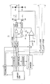
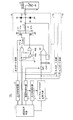
- FIG. 1 is a schematic diagram showing a configuration of a semiconductor processing apparatus according to Embodiment 1 of the present invention.
- a semiconductor processing device 10 shown in FIG. 1 includes an arithmetic processing circuit 1, a digital / analog conversion circuit 2, an output control circuit 3, a plurality of output port circuits 4, a connection control circuit 5, and an output switching circuit 6.
- the configuration is not limited to a configuration in which a plurality of output port circuits 4 are connected to one digital / analog conversion circuit 2, but one output port circuit 4 is connected to one digital / analog conversion circuit 2. It may be the configuration.
- the arithmetic processing circuit 1 is a CPU, MPU, or the like, performs desired arithmetic processing based on an input signal, and outputs a digital signal such as a control signal to circuits such as the digital / analog conversion circuit 2 and the output control circuit 3. Output.
- the digital / analog conversion circuit 2 converts the digital signal output from the arithmetic processing circuit 1 into an analog signal.
- the output control circuit 3 controls the output of the analog signal converted by the digital / analog conversion circuit 2. For example, the output control circuit 3 presets the voltage of the analog signal to be output from the digital / analog conversion circuit 2 and instructs the digital / analog conversion circuit 2 to output the analog signal converted by the digital / analog conversion circuit 2. To do.
- the output port circuit 4 outputs the digital signal output from the arithmetic processing circuit 1 or the analog signal output from the digital / analog conversion circuit 2 to the outside.
- the output port circuit 4 includes an output buffer 41, an output amplifier 42, a first switch element SW1, and second switch elements SW2 and SW3.
- FIG. 1 the configuration of one output port circuit 4 is illustrated in detail, but the configuration of the other output port circuits 4 is the same, and thus detailed illustration is omitted.
- the output buffer 41 is a CMOS circuit in which a P-channel MOS transistor 41a and an N-channel MOS transistor 41b are connected in series. One end of the P-channel MOS transistor 41a is connected to the power supply and the other end is connected to the N-channel MOS transistor 41b. One end of the N-channel MOS transistor 41b is grounded and the other end is connected to the P-channel MOS transistor 41a. . Since the output buffer 41 is composed of a CMOS circuit generally used for the output port circuit 4 that outputs a digital signal, it is not necessary to use a special circuit and can be manufactured at low cost.
- the output buffer 41 outputs a digital signal by switching the P channel MOS transistor 41a and the N channel MOS transistor 41b between the on state and the off state. Specifically, the output buffer 41 does not directly output the digital signal output from the arithmetic processing circuit 1 from the output port 43, but converts the digital signal output from the arithmetic processing circuit 1 into a control signal by the logic circuit 44. The output buffer 41 outputs a digital signal by switching the P channel MOS transistor 41a and the N channel MOS transistor 41b between the on state and the off state based on the converted control signal.
- the output buffer 41 outputs the H level digital signal. (2.8V-threshold voltage) is output.
- the output buffer 41 outputs an L level digital signal (0 V + threshold voltage).
- the logic circuit 44 is connected to one input terminal of the NAND circuit 44a connected to the gate terminal of the P-channel MOS transistor 41a, the NOR circuit 44b connected to the gate terminal of the N-channel MOS transistor 41b, and the NOR circuit 44b.
- a NOT circuit 44c is provided.
- the output buffer 41 is not limited to a CMOS circuit, and may be a transistor circuit that has at least one transistor and outputs a digital signal by switching between the on state and the off state of the transistor. Any circuit may be used, for example, an open-drain output circuit having an N-channel MOS transistor.
- the output amplifier 42 amplifies the analog signal output from the digital / analog conversion circuit 2.
- the first switch element SW1 is provided between the digital / analog conversion circuit 2 and the output amplifier 42, and based on the control signal output from the connection control circuit 5, the connection between the digital / analog conversion circuit 2 and the output amplifier 42, Switch between cutting.
- the second switch elements SW2 and SW3 are connected to the gate terminals of the P-channel MOS transistor 41a and the N-channel MOS transistor 41b, and are connected to the arithmetic processing circuit 1 side based on the switching signal output from the output switching circuit 6 or output The connection to the amplifier 42 side is switched.
- the output port circuit 4 when the first switch element SW1 is turned on, the digital / analog conversion circuit 2 and the output amplifier 42 are connected, and an analog signal output from the digital / analog conversion circuit 2 is input to the output amplifier 42. To do. Further, the output port circuit 4 has an analog amplified by the output amplifier 42 when the second switch elements SW2 and SW3 are connected to the output amplifier 42 side (when the output buffer 41 and the output amplifier 42 are connected). A signal is input to the gate terminals of P channel MOS transistor 41a and N channel MOS transistor 41b. Output port circuit 4 controls the on resistance of P channel MOS transistor 41a and N channel MOS transistor 41b.
- the output port circuit 4 takes into account the threshold voltage of each MOS transistor and supplies the voltage (2.8V) supplied as the power supply voltage. ) And the ground voltage (0 V), an analog signal within a voltage range can be output from the output buffer 41.
- the second switch elements SW2 and SW3 are connected to the arithmetic processing circuit 1 side (when the output buffer 41 and the logic circuit 44 are connected)
- the output port circuit 4 receives the digital signal from the output buffer 41. Can be output.
- the output port circuit 4 includes an output port 43 that outputs a digital signal or an analog signal output from the output buffer 41 to the outside.
- a protection diode 45 is connected between the output buffer 41 and the output port 43 in order to prevent the output port circuit 4 from being damaged by an external signal input to the output port 43.
- the output port circuit 4 comprises an output amplifier 42 as an operational amplifier, an analog signal output from the digital-analog conversion circuit 2 at the positive input terminal, and an analog signal output from the output buffer 41 at the negative input terminal. Enter each.
- the output amplifier 42 changes the amplification factor of the analog signal based on the result of comparing the voltage of the analog signal output from the output buffer 41 and the voltage of the analog signal output from the digital-analog conversion circuit 2.
- feedback control can be performed so that the analog signal output from the output buffer 41 matches the analog signal output from the digital / analog conversion circuit 2.
- the digital / analog conversion circuit 2 In order to output an analog signal from the digital signal, the digital / analog conversion circuit 2 does not need to convert the digital signal again to an analog signal, and the error of the digital / analog conversion circuit 2 generated in the analog signal output from the reference circuit can be reduced. It becomes possible. Therefore, the semiconductor processing apparatus 10 can perform highly accurate feedback control so that the analog signal output from the output buffer 41 matches the analog signal output from the digital / analog conversion circuit 2.
- the output port circuit 4 has a capacitor CAP that holds the voltage of the analog signal output from the digital / analog conversion circuit 2 when the digital / analog conversion circuit 2 and the output amplifier 42 are connected by the first switch element SW1. Prepare. Since the output port circuit 4 includes the capacitor CAP, when the output amplifier 42 compares the voltage of the analog signal output from the output buffer 41 with the voltage of the analog signal output from the digital / analog conversion circuit 2, There is no need to connect the digital / analog conversion circuit 2 and the output buffer 41. That is, the output amplifier 42 can perform feedback control by comparing the voltage of the analog signal output from the output buffer 41 with the voltage of the analog signal output from the digital-analog conversion circuit 2 held in the capacitor CAP. it can.
- the semiconductor processing apparatus 10 disconnects the digital / analog conversion circuit 2 and the output amplifier 42 and outputs an analog signal from the next output port circuit 4 before completing the feedback control of one output port circuit 4. can do.
- the output amplifier 42 is affected by the voltage fluctuation of the analog signal output from the digital / analog conversion circuit 2 because the digital / analog conversion circuit 2 and the output amplifier 42 are disconnected when performing feedback control. And feedback control can be performed. Note that the voltage of the analog signal held in the capacitor CAP fluctuates due to leakage current and other factors, so the analog signal voltage output from the digital / analog conversion circuit 2 may be held again at a predetermined cycle.
- the connection control circuit 5 controls the connection between the digital / analog conversion circuit 2 and the output port circuit 4. Specifically, the connection control circuit 5 controls the connection between the digital / analog conversion circuit 2 and the output port circuit 4 by switching between the ON state and the OFF state of the first switch element SW1 based on the output control signal. ing.
- the output switching circuit 6 switches whether to output a digital signal or an analog signal from the output port circuit 4 to the outside. Specifically, the output switching circuit 6 switches whether the second switch elements SW2 and SW3 are connected to the arithmetic processing circuit 1 side or the output amplifier 42 side based on the output switching signal, and outputs the output port.
- the circuit 4 switches whether to output a digital signal or an analog signal to the outside.
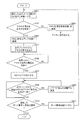
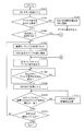
- FIG. 2 is a flowchart for explaining the operation of the semiconductor processing apparatus 10 according to the first embodiment of the present invention.
- the output control circuit 3 presets the voltage of an analog signal to be output from the digital / analog conversion circuit 2.
- the connection control circuit 5 turns on the first switch element SW1 (step S201).
- the output control circuit 3 instructs the digital / analog conversion circuit 2 to output the analog signal converted by the digital / analog conversion circuit 2.
- the output switching circuit 6 determines whether or not an instruction to output an analog signal from the output port circuit 4 has been issued from the arithmetic processing circuit 1 (step S202).
- the output switching circuit 6 calculates the second switch elements SW2 and SW3. Connect to the processing circuit 1 side (step S203).
- the semiconductor processing apparatus 10 outputs a digital signal from the output port circuit 4 by connecting the second switch elements SW2 and SW3 to the arithmetic processing circuit 1 side.
- the output switching circuit 6 determines that an instruction to output an analog signal from the output port circuit 4 is issued from the arithmetic processing circuit 1 (step S202: YES)
- the output switching circuit 6 outputs the second switch elements SW2 and SW3. Connect to the amplifier 42 side (step S204).
- the semiconductor processing apparatus 10 outputs an analog signal from the output buffer 41 of the output port circuit 4 (step S205).
- the output port circuit 4 determines whether or not the voltage of the analog signal output from the digital / analog conversion circuit 2 is held in the capacitor CAP (step S206). When the output port circuit 4 determines that the voltage of the analog signal output from the digital / analog conversion circuit 2 is not held in the capacitor CAP (step S206: NO), the output port circuit 4 repeats the process of step S206. .
- step S206 When the output port circuit 4 determines that the voltage of the analog signal output from the digital / analog conversion circuit 2 is held in the capacitor CAP (step S206: YES), the connection control circuit 5 turns off the first switch element SW1. (Step S207). The output control circuit 3 instructs the digital / analog conversion circuit 2 to stop outputting the analog signal converted by the digital / analog conversion circuit 2.
- the output amplifier 42 compares the voltage of the analog signal output from the output buffer 41 with the voltage of the analog signal held in the capacitor CAP (the voltage of the analog signal output from the digital / analog conversion circuit 2), and matches. It is determined whether or not it has been done (step S208).
- the output amplifier 42 determines that the voltage of the analog signal output from the output buffer 41 does not match the voltage of the analog signal held in the capacitor CAP (step S208: NO)
- the output amplifier 42 The amplification factor of the analog signal is changed based on the difference (comparison result) between the voltage of the analog signal output from 41 and the voltage of the analog signal held in the capacitor CAP (step S209).
- step S209 the output amplifier 42 returns to the process of step S208 and compares the voltage of the analog signal output from the output buffer 41 after changing the amplification factor of the analog signal with the voltage of the analog signal held in the capacitor CAP. Then, it is determined again whether or not they match.
- step S208: YES When the output amplifier 42 determines that the voltage of the analog signal output from the output buffer 41 matches the voltage of the analog signal held in the capacitor CAP (step S208: YES), the output amplifier 42 repeats feedback control. . By repeating such feedback control, the semiconductor processing apparatus 10 stably outputs an analog signal having a desired voltage from the output port circuit 4. Although the case where an analog signal is output from one output port circuit 4 has been described, analog signals can be output from a plurality of output port circuits 4 by repeating the same processing for other output port circuits 4. it can.
- the output control circuit 3 presets the voltage of the analog signal to be output from the digital-analog conversion circuit 2 for each output port circuit 4, so that the P-channel MOS transistor 41 a and the N-channel are set for each output port circuit 4.
- the on-resistance of the MOS transistor 41b can be controlled.
- the semiconductor processing apparatus 10 controls the on-resistance of the output buffer 41 that outputs a digital signal and outputs an analog signal from the output buffer 41.
- An analog signal can be output from the output port circuit 4 for output. Therefore, in the semiconductor processing apparatus 10, the output port circuit 4 that outputs a digital signal and the output port circuit 4 that outputs an analog signal can be shared, and the number of the output port circuits 4 can be reduced to reduce the size. Can do.
- the semiconductor processing apparatus 10 outputs the analog signal output from the digital / analog conversion circuit 2 from the output port circuit 4 using the output buffer 41, a circuit connected to the output port circuit 4 (for example, a memory circuit, The impedance of the sensor circuit and the like and the impedance of the digital / analog conversion circuit 2 do not need to be matched, and a plurality of output port circuits 4 can be provided for one digital / analog conversion circuit 2.
- the semiconductor processing apparatus 10 controls each on-resistance of the P-channel MOS transistor 41a and the N-channel MOS transistor 41b of the output buffer 41 for each output port circuit 4, the semiconductor processing apparatus 10 outputs an analog signal. An analog signal with a different voltage can be output from the output buffer 41.
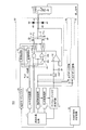
- FIG. 3 is a schematic diagram showing the configuration of the semiconductor processing apparatus according to the second embodiment of the present invention.
- the semiconductor processing apparatus 11 shown in FIG. 3 includes an arithmetic processing circuit 1, a digital / analog conversion circuit 2, an output control circuit 3, a plurality of output port circuits 4, a connection control circuit 5, and an output switching circuit 6.
- the semiconductor processing apparatus 11 has the same configuration as the semiconductor processing apparatus 10 according to the first embodiment of the present invention, except that it includes an output amplifier 48. Therefore, the same components are denoted by the same reference numerals and detailed description thereof is omitted.
- the output amplifier 42 shown in FIG. 1 outputs the same analog signal to each of the second switch elements SW2 and SW3. That is, the output amplifier 42 outputs the same analog signal to the gate terminals of the P channel MOS transistor 41a and the N channel MOS transistor 41b, so that the output buffer 41 uses the P channel MOS transistors 41a and N based on the same analog signal.
- the on-resistance of the channel MOS transistor 41b is controlled.
- the output amplifier 48 shown in FIG. 3 can output a positive level analog signal and an inverted level analog signal, and a positive level analog signal is output to the second switch element SW2. Invert level analog signals are respectively output to the second switch elements SW3. That is, the output amplifier 48 outputs different analog signals to the gate terminal of the P-channel MOS transistor 41a and the gate terminal of the N-channel MOS transistor 41b, so that the output buffer 41 can generate P based on the different analog signals.
- the on resistance of channel MOS transistor 41a and the on resistance of N channel MOS transistor 41b can be individually controlled.
- the semiconductor processing apparatus 11 is not limited to a configuration in which a plurality of output port circuits 4 are connected to one digital / analog conversion circuit 2.
- the output port circuit 4 may be connected.
- the semiconductor processing apparatus 11 may have a configuration in which the output port circuit 4 including the output amplifier 42 and the output port circuit 4 including the output amplifier 48 are mixed. Furthermore, since the operation of the semiconductor processing apparatus 11 is the same as the operation of the semiconductor processing apparatus 10 according to the first embodiment, detailed description thereof is omitted.
- the output amplifier 48 is different from the P-channel MOS transistor 41a of the output buffer 41 and the N-channel MOS transistor 41b of the output buffer 41. Since an analog signal is output, the on-resistance of the P-channel MOS transistor 41a and the on-resistance of the N-channel MOS transistor 41b can be individually controlled based on different analog signals, and the analog signal output from the output buffer 41 can be controlled. Can be controlled with high accuracy.
- control signals from the output amplifier 42 or the output amplifier 48 to the second switch elements SW2 and SW3 will be described as the configuration shown in the drawing corresponding to the first embodiment. However, the configuration shown in the drawing corresponding to the second embodiment is also included.
- FIG. 4 is a schematic diagram showing the configuration of the connection control circuit 50 of the semiconductor processing apparatus according to the third embodiment of the present invention. 4, in addition to the connection control circuit 50, the digital / analog conversion circuit 2, the output control circuit 3, and the first switch element SW1 of the output port circuit are illustrated.
- the constituent elements of the semiconductor processing apparatus according to the third embodiment not shown in FIG. 4 are the same as the constituent elements of the semiconductor processing apparatus 10 according to the first embodiment shown in FIG. This will be described below using the same reference numerals.
- the connection control circuit 50 shown in FIG. 4 includes a counter 51 and a register 52 that stores the port number of the output port circuit 4.
- the counter 51 sequentially selects the port numbers of the output port circuit 4 stored in the register 52 at regular intervals.
- the register 52 outputs a control signal corresponding to the port number of the output port circuit 4 selected by the counter 51 to the output control circuit 3 and the first switch element SW1 of the output port circuit 4.
- the output control circuit 3 and the first switch element SW1 of the output port circuit 4 include registers 31 and 49 that store processing information corresponding to the port numbers of the output port circuit 4, respectively. Therefore, the output control circuit 3 and the first switch element SW1 of the output port circuit 4 execute processing information corresponding to the port number of the output port circuit 4 based on the control signal output from the connection control circuit 50 (register 52). To do.
- the output control circuit 3 and the first switch element SW1 of the output port circuit 4 are connected to the port number of the output port circuit 4.
- the processing information stored in the registers 31 and 49 corresponding to P0 is executed.
- the output control circuit 3 executes the processing information stored in the register 31 to preset the voltage of the analog signal desired to be output from the digital / analog conversion circuit 2 and convert the analog signal converted by the digital / analog conversion circuit 2 Is output to the digital / analog conversion circuit 2.
- the first switch element SW1 of the output port circuit 4 is changed from the off state to the on state by executing the processing information stored in the register 49. Similar processing is performed for the port numbers P1 to P3 of the output port circuit 4 by the counter 51 sequentially selecting the port numbers of the output port circuit stored in the register 52 at regular intervals.
- the port number of the output port circuit 4 is not limited to P0 to P3.
- FIG. 5 is a flowchart for explaining the operation of the semiconductor processing apparatus according to the third embodiment of the present invention.
- the counter 51 selects one of the port numbers of the output port circuit 4 stored in the register 52.
- the output control circuit 3 executes processing information stored in the register 31 corresponding to the port number of the output port circuit 4 selected by the counter 51.
- the output control circuit 3 executes the processing information stored in the register 31 and presets the voltage of the analog signal desired to be output from the digital / analog conversion circuit 2.
- the connection control circuit 5 turns on the first switch element SW1 corresponding to the port number of the output port circuit 4 selected by the counter 51 (step S501).
- the output control circuit 3 executes the processing information stored in the register 31 and instructs the digital / analog conversion circuit 2 to output the analog signal converted by the digital / analog conversion circuit 2.
- the output switching circuit 6 determines whether or not an instruction to output an analog signal from the output port circuit 4 has been issued from the arithmetic processing circuit 1 (step S502).
- the output switching circuit 6 calculates the second switch elements SW2 and SW3. Connect to the processing circuit 1 side (step S503).
- the semiconductor processing apparatus outputs a digital signal from the output port circuit 4 by connecting the second switch elements SW2 and SW3 to the arithmetic processing circuit 1 side.
- step S502 When the output switching circuit 6 determines that an instruction to output an analog signal from the output port circuit 4 is from the arithmetic processing circuit 1 (step S502: YES), the output switching circuit 6 outputs the second switch elements SW2 and SW3. Connection is made to the amplifier 42 side (step S504).
- the semiconductor processing apparatus outputs an analog signal from the output port circuit 4 by connecting the second switch elements SW2 and SW3 to the output amplifier 42 side (step S505).
- the output port circuit 4 determines whether or not the voltage of the analog signal output from the digital / analog conversion circuit 2 is held in the capacitor CAP (step S506).
- the output port circuit 4 determines that the voltage of the analog signal output from the digital / analog conversion circuit 2 is not held in the capacitor CAP (step S506: NO)
- the output port circuit 4 repeats the process of step S506. .
- step S506 When the output port circuit 4 determines that the voltage of the analog signal output from the digital / analog conversion circuit 2 is held in the capacitor CAP (step S506: YES), the connection control circuit 5 selects the output port circuit selected by the counter 51. The first switch element SW1 corresponding to the port number 4 is turned off (step S507). The output control circuit 3 executes the processing information stored in the register 31 and instructs the digital / analog conversion circuit 2 to stop outputting the analog signal converted by the digital / analog conversion circuit 2.
- the output amplifier 42 compares the voltage of the analog signal output from the output buffer 41 with the voltage of the analog signal held in the capacitor CAP (the voltage of the analog signal output from the digital / analog conversion circuit 2), and matches. It is determined whether or not it has been done (step S508).
- the output amplifier 42 determines that the voltage of the analog signal output from the output buffer 41 does not match the voltage of the analog signal held in the capacitor CAP (step S508: NO)
- the output amplifier 42 The amplification factor of the analog signal is changed based on the difference (comparison result) between the voltage of the analog signal output from 41 and the voltage of the analog signal held in the capacitor CAP (step S509).
- step S509 the output amplifier 42 returns to the process of step S206, and compares the voltage of the analog signal output from the output buffer 41 after changing the amplification factor of the analog signal with the voltage of the analog signal held in the capacitor CAP. Then, it is determined again whether or not they match.
- step S508 determines that the voltage of the analog signal output from the output buffer 41 matches the voltage of the analog signal held in the capacitor CAP (step S508: YES)
- the counter 51 selects the selected output port circuit. It is determined whether the port number 4 exceeds a predetermined number (step S510).
- the semiconductor processing apparatus 10 repeats feedback control (step S508). )
- An analog signal having a desired voltage is stably output from the output port circuit 4.
- step S510: NO the counter 51 increments the port number of the selected output port circuit 4 by one (step S510: NO).
- Step S511 For example, the counter 51 increments the port number of the selected output port circuit 4 from P0 to P1. After the counter 51 increments the port number of the output port circuit 4 to be selected by one, the process returns to step S501.
- step S510: YES the semiconductor processing apparatus ends the process.
- the connection control circuit 5 sequentially selects the port number of the output port circuit 4 set corresponding to each of the plurality of output port circuits 4.
- Counter 51 is provided.
- the output control circuit 3 presets the voltage of the analog signal to be converted by the digital / analog conversion circuit 2 corresponding to the port number of the output port circuit 4 selected by the counter 51, and the connection control circuit 5 selects by the counter 51 Since the first switch element SW1 of the output port circuit 4 corresponding to the port number of the output port circuit 4 is turned on, it is not necessary for the arithmetic processing circuit 1 to perform processing for sequentially switching the plurality of output port circuits 4, and The burden of processing by the processing circuit 1 can be reduced.
- the semiconductor processing apparatus sequentially selects the port number of the output port circuit 4 by the counter 51.
- the voltage of the analog signal output from the digital / analog conversion circuit 2 held in the capacitor CAP can be sequentially supplied. Therefore, the semiconductor processing apparatus can stably hold the voltage of the analog signal output from the digital / analog conversion circuit 2 in the capacitor CAP, so that the voltage of the analog signal output from the output buffer 41 is controlled with high accuracy. be able to.
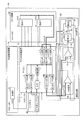
- FIG. 6 is a schematic diagram showing a configuration of a semiconductor processing system according to Embodiment 4 of the present invention.
- a semiconductor processing system 100 shown in FIG. 6 includes a semiconductor processing device 12, a memory circuit 60, an external connection circuit 70, a communication circuit 80, and an arithmetic circuit 90.
- the semiconductor processing apparatus 12 is the semiconductor processing apparatus described in the first to third embodiments, and can output a digital signal or an analog signal from the output port circuit 4. Further, the semiconductor processing device 12 supplies an analog signal from the output port circuit 4 to the memory circuit 60, the external connection circuit 70, the communication circuit 80, and the arithmetic circuit 90 to be connected, and functions as a power source. is doing.
- the semiconductor processing apparatus 12 is supplied with a voltage of 5.0 V from an external power source.
- the memory circuit 60 is a storage circuit such as a DRAM, for example, and includes two general-purpose ICs 61 driven at a voltage of 3.3V.
- the general-purpose IC 61 inputs an analog signal having a voltage of 3.3 V from the output port circuit 4 of the semiconductor processing apparatus 12 to the VCC terminal for driving.
- the general-purpose IC 61 requires a large current to drive a memory element (not shown), but the analog signal current output from the output port circuit 4 is smaller than the large current driving the memory element. Therefore, the semiconductor processing system 100 supplies a large current necessary for the general-purpose IC 61 by connecting the plurality of output port circuits 4 to the memory circuit 60.
- the three output port circuits 4 are connected to the memory circuit 60.
- a large current required for the general-purpose IC 61 is supplied.
- the memory circuit 60 and the semiconductor processing device 12 are connected to other than the output port circuit 4 in order to transmit and receive data between the memory circuit 60 and the semiconductor processing device 12.
- the external connection circuit 70 is an interface circuit for connecting to an external storage device, for example, and includes one general-purpose IC 71 driven at a voltage of 1.8V.
- the general-purpose IC 71 inputs an analog signal having a voltage of 1.8 V from the output port circuit 4 of the semiconductor processing apparatus 12 to the VCC terminal for driving.
- the communication circuit 80 is a communication port that performs data communication with an external device, for example, and is a circuit that can supply a voltage of 2.7 V to the connected external device.
- the communication circuit 80 inputs an analog signal having a voltage of 2.7 V from the output port circuit 4 of the semiconductor processing apparatus 12 in order to supply a voltage of 2.7 V to the external device.
- the communication circuit 80 is connected to a serial input / output port (SI / O) 7 of the semiconductor processing apparatus 12 in order to perform data communication between the semiconductor processing apparatus 12 and an external device.
- SI / O serial input / output port
- the arithmetic circuit 90 is an arithmetic circuit that arithmetically processes, for example, a digital signal output from the semiconductor processing device 12, and includes an arithmetic unit 93 having a first IC 91 and a second IC 92, and a first power supply detection circuit 94 that detects a rise in power supply of the first IC 91. , And a second power source detection circuit 95 for detecting the rise of the power source of the second IC 92. Each of the first IC 91 and the second IC 92 outputs a voltage corresponding to the supplied voltage level as an operation enable signal (EN signal).
- EN signal operation enable signal
- the arithmetic circuit 90 first inputs a voltage of 1.5 V from the output port circuit 4B, and inputs an analog signal of a voltage of 1.8 V from the output port circuit 4A to the first IC 91, thereby driving the first IC 91.
- the first IC 91 outputs an operation enable signal (EN signal) to the first power supply detection circuit 94.
- the first power supply detection circuit 94 compares the analog signal (reference voltage) of the voltage 1.5V output from the output port circuit 4B with the EN signal voltage of the first IC 91, and the EN signal voltage is higher than the reference voltage.
- the first detection signal that detects the rise of the power supply of the first IC 91 is output to the semiconductor processing device 12. In a certain period immediately after the power is turned on, the switch 96 is in an off state.
- the semiconductor processing device 12 changes the output port circuit 4B to the digital output operation state based on the first detection signal, and outputs an H voltage (eg, 2.2 V) for turning on the switch 96 of the arithmetic unit 93. Then, the switch 96 is turned on.
- the switch 96 is configured to have hysteresis characteristics, and configures a voltage that changes from the off state to the on state to 2.0V, and a voltage that changes from the on state to the off state to 1.0V. Thereafter, the output port circuit 4B is changed to the analog output operation state, and the output of the reference voltage 1.5V of the second power supply detection circuit 95 is started.
- the second IC 92 is driven by inputting an analog signal having a voltage of 1.8 V to the second IC 92 from the output port circuit 4A.
- the second IC 92 outputs an operation enable signal (EN2 signal) to the second power supply detection circuit 95.
- the second power supply detection circuit 95 compares the analog signal (reference voltage) of voltage 1.5V output from the output port circuit 4B with the voltage of the EN2 signal of the first IC 91, and the voltage of the EN2 signal is higher than the reference voltage.
- the second detection signal that detects the rise of the power supply of the second IC 92 is output to the semiconductor processing device 12.
- the semiconductor processing device 12 sequentially outputs a data transfer start signal (start signal) and a digital signal from the output port circuit 4B to the first IC 91 based on the second detection signal.
- the semiconductor processing device 12 controls the on-resistance of the P-channel MOS transistor 41a and the N-channel MOS transistor 41b for each output port circuit 4, and outputs an analog signal from the output buffer 41. Since the signals are output, analog signals having different voltages can be output from the output buffers 41 of the respective output port circuits 4. Therefore, the semiconductor processing apparatus 12 is driven with a memory circuit 60 driven with a voltage of 3.3 V, an external connection circuit 70 driven with a voltage of 1.8 V, a communication circuit 80 that supplies a voltage of 2.7 V, and a voltage of 1.8 V. An arithmetic circuit 90 that requires a reference voltage of 0.8 V can be connected to the output port circuit 4.
- the voltage at the time of analog signal output is set to 1.5V
- the H voltage at the time of digital signal output is set to 2.2V, so that 1.5V
- the semiconductor processing system 100 includes the semiconductor processing apparatus 12 that can output analog signals of different voltages from the output buffers 41 of the plurality of output port circuits 4. Therefore, it is possible to connect a circuit driven by analog signals of different voltages to the semiconductor processing device 12 without providing a plurality of digital / analog conversion circuits, voltage conversion circuits, and the like. By switching the output state, it becomes easy to output different voltages, and the semiconductor processing system 100 can be downsized. In addition, when the first IC 91 and the second IC 92 are started to operate simultaneously, power consumption increases and troubles such as noise generation occur.
- the semiconductor processing system 100 includes the first IC 91 and the second IC 92. An appropriate time difference can be easily set at the start of the operation.
- FIG. 7 is a schematic diagram showing the configuration of the semiconductor processing apparatus according to the fifth embodiment of the present invention.
- the semiconductor processing apparatus 13 shown in FIG. 7 has a configuration in which a peripheral function circuit 8 is added to the configuration of the semiconductor processing apparatus 10 shown in FIG.
- the peripheral function circuit 8 includes a timer circuit, a PWM (Pulse Width Modulation) circuit, and the like.
- the output port circuit 4 can switch the digital signal output from the arithmetic processing circuit 1, the analog signal output from the digital / analog conversion circuit 2, and the digital signal output from the peripheral function circuit 8.
- the output port circuit 4 includes a fourth switch element SW4 and a fifth switch element SW5 in order to switch between a digital signal output from the arithmetic processing circuit 1 and a digital signal output from the peripheral function circuit 8.
- the fourth switch element SW4 and the fifth switch element SW5 are switching elements for switching the connection between the arithmetic processing circuit 1 and the logic circuit 44 to the connection between the peripheral function circuit 8 and the logic circuit 44.
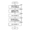
- FIG. 8 is a flowchart for explaining the operation of the semiconductor processing apparatus according to the fifth embodiment of the present invention.
- the arithmetic processing circuit 1 outputs a digital signal using the output port circuit 4 (step S801). Thereafter, the arithmetic processing circuit 1 ends the use of the output port circuit 4, and the arithmetic processing circuit 1 outputs a start signal for starting the peripheral function circuit 8 to the peripheral function circuit 8 (step S802).
- the peripheral function circuit 8 switches the fourth switch element SW4 and the fifth switch element SW5 in order to complete the activation and output the digital signal (step S803).
- the peripheral function circuit 8 outputs an output switching signal to each of the fourth switch element SW4 and the fifth switch element SW5, and connects the arithmetic processing circuit 1 and the logic circuit 44 to the peripheral function circuit 8. The connection to the logic circuit 44 is switched.
- the peripheral function circuit 8 needs to output the peripheral function output enable signal to the output switching circuit 6 and switch the second switch elements SW2 and SW3 so that the output buffer 41 and the logic circuit 44 are connected.
- the peripheral function circuit 8 switches the fourth switch element SW4 and the fifth switch element SW5, and then outputs a digital signal using the output port circuit 4 (step S804). After that, when the peripheral function circuit 8 terminates the use of the output port circuit 4 and the digital-analog conversion circuit 2 performs an analog signal output using the output port circuit 4, the peripheral function circuit 8 determines that the peripheral function output is valid. The signal is output to the output switching circuit 6, and the second switch elements SW2 and SW3 are switched so that the output buffer 41 and the digital / analog conversion circuit 2 are connected (step S805).
- the semiconductor processing apparatus 13 uses the output port circuit 4 by providing the output port circuit 4 with the fourth switch element SW4 and the fifth switch element SW5. Digital signal output from the arithmetic processing circuit 1 and digital signal output from the peripheral function circuit 8 can also be performed.
- a predetermined voltage is supplied by outputting an analog signal from the output port circuit 4 to the memory circuit 60, the external connection circuit 70, the communication circuit 80, and the arithmetic circuit 90. It functions as a power source.
- the semiconductor processing apparatus 12 that functions as a power source is roughly divided into a power source (reference power source) that supplies a reference voltage and a power source (current source) that supplies a current.
- the semiconductor processing device 12 outputs an analog signal with a voltage of 1.5 V output from the output port circuit 4B to the first power supply detection circuit 94 and the second power supply detection circuit 95 of the arithmetic circuit 90 as a reference voltage. is doing.
- the semiconductor processing device 12 outputs an analog signal of voltage 3.3V output from the output port circuit 4B as a power supply voltage to the memory circuit 60, the external connection circuit 70, and the like, and supplies a current to drive the memory element. Supply.
- FIG. 9 is a schematic diagram showing the configuration of the semiconductor processing apparatus according to the sixth embodiment of the present invention.
- the semiconductor processing apparatus 10a shown in FIG. 9 includes an arithmetic processing circuit 1, a digital / analog conversion circuit 2, an output control circuit 3, a plurality of output port circuits 4a, a connection control circuit 5, and an output switching circuit 6.
- the semiconductor processing apparatus 10a has the same configuration as the semiconductor processing apparatus 10 according to the first embodiment of the present invention, except for the configuration of the output port circuit 4a. Therefore, the same components are denoted by the same reference numerals and detailed description thereof is omitted.
- the output port circuit 4 shown in FIG. 1 has second switch elements SW2 and SW3 connected to the gate terminals of the P-channel MOS transistor 41a and the N-channel MOS transistor 41b. Based on the switching signal output from the output switching circuit 6, the second switch elements SW2 and SW3 switch whether to connect to the arithmetic processing circuit 1 side or to the output amplifier 42 side.
- the output port circuit 4 shown in FIG. 1 is amplified by the output amplifier 42 when the second switch elements SW2 and SW3 are connected to the output amplifier 42 side (when the output buffer 41 and the output amplifier 42 are connected).
- the analog signal is input to the gate terminals of the P-channel MOS transistor 41a and the N-channel MOS transistor 41b.
- Output port circuit 4 shown in FIG. 1 controls the on-resistances of P channel MOS transistor 41a and N channel MOS transistor 41b. By controlling the on-resistances of the P-channel MOS transistor 41a and the N-channel MOS transistor 41b, the output port circuit 4 shown in FIG. 1 takes into account the threshold voltage of each MOS transistor and is supplied as a power supply voltage.
- the output buffer 41 can output an analog signal within a voltage range between the voltage and the ground voltage.
- a general-purpose IC is connected to the output port circuit 4 shown in FIG. 1, and the semiconductor processing apparatus 10 is caused to function as a power source for supplying a current for driving the general-purpose IC.
- the semiconductor processing apparatus 10 in addition to the current I1 flowing from the power supply to the general-purpose IC via the P-channel MOS transistor 41a, a current I2 flowing from the power supply to the ground via the P-channel MOS transistor 41a and the N-channel MOS transistor 41b is always required. For this reason, the semiconductor processing apparatus 10 has a problem that the current consumed increases because it is necessary to pass the current I1 + I2 in order to drive the general-purpose IC.
- the output port circuit 4a is provided instead of the output port circuit 4 shown in FIG.
- the output port circuit 4a shown in FIG. 9 has a second switch element SW2 connected to the gate terminal of the P-channel MOS transistor 41a. That is, the second switch element SW3 is not connected to the gate terminal of the N-channel MOS transistor 41b, and the NOR circuit 44b of the logic circuit 44 is directly connected to the gate terminal of the N-channel MOS transistor 41b. Based on the switching signal output from the output switching circuit 6, the second switch element SW2 switches whether to connect to the arithmetic processing circuit 1 side or to the output amplifier 42 side.
- the output port circuit 4a converts the analog signal amplified by the output amplifier 42 to P Input to the gate terminal of the channel MOS transistor 41a.
- Output port circuit 4a controls the on-resistance of P-channel MOS transistor 41a.
- the output port circuit 4a When the general-purpose IC 9 is connected to the output port circuit 4a, the output port circuit 4a outputs an analog signal from the output buffer 41 by controlling the on-resistance of the P-channel MOS transistor 41a, and supplies a current to the general-purpose IC 9. Can be supplied.
- the voltage of the analog signal output from the output port circuit 4a is a value obtained by dividing the power supply voltage based on the ON resistance of the P-channel MOS transistor 41a and the ON resistance of the general-purpose IC 9.
- N channel MOS transistor 41b is turned off when NOR circuit 44b outputs logic L as an off signal. If the off-leakage channel current flowing through the N-channel MOS transistor 41b due to process variations is taken into account, the logic L output from the NOR circuit 44b may be a negative voltage. The same applies to the semiconductor processing apparatus according to the embodiment described below.
- the semiconductor processing device 10a When the general-purpose IC 9 is connected to the output port circuit 4a and the semiconductor processing device 10a functions as a power source for supplying a current for driving the general-purpose IC 9, the current flowing from the power source to the general-purpose IC 9 via the P-channel MOS transistor 41a Only I1 is required. That is, since N channel MOS transistor 41b is in an off state, current I2 flowing from the power supply to ground via P channel MOS transistor 41a and N channel MOS transistor 41b is not necessary. Therefore, since the semiconductor processing apparatus 10a can drive the general-purpose IC 9 only by flowing the current I1, the consumed current can be reduced.
- FIG. 10 is a flowchart for explaining the operation of the semiconductor processing apparatus 10a according to the sixth embodiment of the present invention.
- the output control circuit 3 presets the voltage of an analog signal to be output from the digital / analog conversion circuit 2.
- the connection control circuit 5 turns on the first switch element SW1 (step S201).
- the output control circuit 3 instructs the digital / analog conversion circuit 2 to output the analog signal converted by the digital / analog conversion circuit 2.
- the output switching circuit 6 determines whether or not there has been an instruction from the arithmetic processing circuit 1 to output an analog signal from the output port circuit 4a (step S202).
- the output switching circuit 6 determines that the instruction to output the analog signal from the output port circuit 4a is not received from the arithmetic processing circuit 1 (step S202: NO)
- the output switching circuit 6 sets the second switch element SW2 to the arithmetic processing circuit. 1 side is connected (step S203a).
- the semiconductor processing apparatus 10a outputs a digital signal from the output port circuit 4a by connecting the second switch element SW2 to the arithmetic processing circuit 1 side.
- the output switching circuit 6 determines that an instruction to output an analog signal from the output port circuit 4a is received from the arithmetic processing circuit 1 (step S202: YES)
- the output switching circuit 6 connects the second switch element SW2 to the output amplifier 42.
- Step S204a Note that when the output switching circuit 6 connects the second switch element SW2 to the output amplifier 42 side, the logic circuit 44 turns off the N-channel MOS transistor 41b.
- the semiconductor processing apparatus 10a outputs an analog signal from the output buffer 41 of the output port circuit 4a (step S205). At this time, the semiconductor processing apparatus 10a outputs an analog signal having a value obtained by dividing the power supply voltage based on the ON resistance of the P-channel MOS transistor 41a and the ON resistance of the general-purpose IC 9 from the output port circuit 4a.
- the output port circuit 4a determines whether or not the voltage of the analog signal output from the digital / analog conversion circuit 2 is held in the capacitor CAP (step S206). When the output port circuit 4a determines that the voltage of the analog signal output from the digital / analog conversion circuit 2 is not held in the capacitor CAP (step S206: NO), the output port circuit 4a repeats the process of step S206. .
- step S206 When the output port circuit 4a determines that the voltage of the analog signal output from the digital / analog conversion circuit 2 is held in the capacitor CAP (step S206: YES), the connection control circuit 5 turns off the first switch element SW1. (Step S207). The output control circuit 3 instructs the digital / analog conversion circuit 2 to stop outputting the analog signal converted by the digital / analog conversion circuit 2.
- the output amplifier 42 compares the voltage of the analog signal output from the output buffer 41 with the voltage of the analog signal held in the capacitor CAP (the voltage of the analog signal output from the digital / analog conversion circuit 2), and matches. It is determined whether or not it has been done (step S208).
- the output amplifier 42 determines that the voltage of the analog signal output from the output buffer 41 does not match the voltage of the analog signal held in the capacitor CAP (step S208: NO)
- the output amplifier 42 The amplification factor of the analog signal is changed based on the difference (comparison result) between the voltage of the analog signal output from 41 and the voltage of the analog signal held in the capacitor CAP (step S209).
- step S209 the output amplifier 42 returns to the process of step S208 and compares the voltage of the analog signal output from the output buffer 41 after changing the amplification factor of the analog signal with the voltage of the analog signal held in the capacitor CAP. Then, it is determined again whether or not they match.
- step S208: YES the output amplifier 42 repeats feedback control. .
- the semiconductor processing apparatus 10a stably outputs an analog signal having a desired voltage from the output port circuit 4a as a current source.
- the output control circuit 3 presets the voltage of the analog signal to be output from the digital-analog conversion circuit 2 for each output port circuit 4a, so that the on-resistance of the P-channel MOS transistor 41a is set for each output port circuit 4a. Can be controlled.
- the semiconductor processing apparatus 10a does not provide the second switch element SW3, and turns off the N-channel MOS transistor 41b that outputs a digital signal in the P-channel state.
- the on-resistance of the MOS transistor 41a is controlled to output an analog signal from the output buffer 41. Therefore, the semiconductor processing apparatus 10a can reduce the current consumed by the output buffer 41 when outputting an analog signal from the output port circuit 4a.
- the semiconductor processing apparatus 10a controls the on-resistance of the P-channel MOS transistor 41a for each output port circuit 4a and outputs an analog signal from the output buffer 41, it differs from the output buffer 41 of each output port circuit 4a. A voltage analog signal can be output.
- the semiconductor processing apparatus 10 a is not limited to the configuration in which a plurality of output port circuits 4 a are connected to one digital / analog conversion circuit 2.
- the output port circuit 4a may be connected.
- the semiconductor processing apparatus 10a may have a configuration in which the output port circuit 4a including the output amplifier 42 and the output port circuit 4a including the output amplifier 48 illustrated in FIG. 3 are mixed.
- FIG. 11 is a schematic diagram showing the configuration of the semiconductor processing apparatus according to the seventh embodiment of the present invention.
- a semiconductor processing device 10b shown in FIG. 11 includes an arithmetic processing circuit 1, a digital / analog conversion circuit 2, an output control circuit 3, a plurality of output port circuits 4b, a connection control circuit 5, an output switching circuit 6, and a power supply mode register 20. I have.
- the semiconductor processing apparatus 10b has the same configuration as the semiconductor processing apparatus 10 according to the first embodiment of the present invention except for the configuration of the output port circuit 4b and the power supply mode register 20. Therefore, the same components are denoted by the same reference numerals and detailed description thereof is omitted.
- the output port circuit 4b is provided instead of the output port circuit 4 shown in FIG. 1, and the power supply mode register 20 is further provided. Reduced.
- the output port circuit 4b shown in FIG. 11 has second switch elements SW2 and SW3 connected to the gate terminals of the P channel MOS transistor 41a and the N channel MOS transistor 41b. Based on the switching signal output from the output switching circuit 6, the second switch element SW2 switches whether to connect to the arithmetic processing circuit 1 side or to the output amplifier 42 side.
- the second switch element SW3 switches between connection to the arithmetic processing circuit 1 side and connection to the output amplifier 42 side based on the switching signal output from the logic circuit A21.
- the power mode register 20 outputs a setting signal for setting the output port circuit 4b to the output port circuit 4b in a power mode for supplying current to the general-purpose IC 9 connected to the output port circuit 4b.
- the setting signal output from the power supply mode register 20 is input to the logic circuit A21 of the output port circuit 4b.
- the logic circuit A21 supplies the second switch element SW3 connected to the gate terminal of the N-channel MOS transistor 41b to the arithmetic processing circuit 1 side. Connecting. Further, the logic circuit A21 controls to output an off signal from the NOR circuit 44b of the logic circuit 44 so that the N-channel MOS transistor 41b is turned off.
- the output port circuit 4b converts the analog signal amplified by the output amplifier 42 to P Input to the gate terminal of the channel MOS transistor 41a.
- Output port circuit 4b controls the on-resistance of P-channel MOS transistor 41a.
- the output port circuit 4b When the general-purpose IC 9 is connected to the output port circuit 4b, the output port circuit 4b outputs an analog signal from the output buffer 41 by controlling the on-resistance of the P-channel MOS transistor 41a, and supplies a current to the general-purpose IC 9. Can be supplied.
- the voltage of the analog signal output from the output port circuit 4b is a value obtained by dividing the power supply voltage based on the ON resistance of the P-channel MOS transistor 41a and the ON resistance of the general-purpose IC 9.
- the semiconductor processing apparatus 10b When the general-purpose IC 9 is connected to the output port circuit 4b and the semiconductor processing apparatus 10b functions as a power source for supplying a current for driving the general-purpose IC 9, the current flowing from the power source to the general-purpose IC 9 via the P-channel MOS transistor 41a Only I1 is required. That is, since N channel MOS transistor 41b is in an off state, current I2 flowing from the power supply to ground via P channel MOS transistor 41a and N channel MOS transistor 41b is not necessary. Therefore, since the semiconductor processing apparatus 10b can drive the general-purpose IC 9 only by flowing the current I1, the consumed current can be reduced.
- FIG. 12 is a flowchart for explaining the operation of the semiconductor processing apparatus 10b according to the seventh embodiment of the present invention.
- the output control circuit 3 presets the voltage of an analog signal to be output from the digital / analog conversion circuit 2.
- the connection control circuit 5 turns on the first switch element SW1 (step S1201).
- the output control circuit 3 instructs the digital / analog conversion circuit 2 to output the analog signal converted by the digital / analog conversion circuit 2.
- the output switching circuit 6 determines whether or not there is an instruction from the arithmetic processing circuit 1 to output an analog signal from the output port circuit 4b (step S1202).
- the output switching circuit 6 determines that the instruction to output the analog signal from the output port circuit 4b has not been received from the arithmetic processing circuit 1 (step S1202: NO)
- the output switching circuit 6 calculates the second switch elements SW2 and SW3. Connection is made to the processing circuit 1 side (step S1203).
- the semiconductor processing apparatus 10b outputs a digital signal from the output port circuit 4b by connecting the second switch elements SW2 and SW3 to the arithmetic processing circuit 1 side.
- the power supply mode register 20 is a general-purpose IC 9 connected to the output port circuit 4b. It is determined whether or not to use as a current source (step S1204).
- the output switching circuit 6 connects the second switch elements SW2 and SW3 to the output amplifier 42 side. (Step S1205). That is, the power supply mode register 20 determines that the power supply mode register 20 is used as a power supply for supplying a reference voltage to the general-purpose IC 9 connected to the output port circuit 4b.
- the semiconductor processing apparatus 10b By connecting the second switch elements SW2 and SW3 to the output amplifier 42 side (step S1205), the semiconductor processing apparatus 10b outputs an analog signal from the output buffer 41 of the output port circuit 4b (step S1206).
- the output port circuit 4b determines whether or not the voltage of the analog signal output from the digital / analog conversion circuit 2 is held in the capacitor CAP (step S1207).
- the output port circuit 4b determines that the voltage of the analog signal output from the digital / analog conversion circuit 2 is not held in the capacitor CAP (step S1207: NO)
- the output port circuit 4b repeats the process of step S1207. .
- the connection control circuit 5 turns off the first switch element SW1. (Step S1208).
- the output control circuit 3 instructs the digital / analog conversion circuit 2 to stop outputting the analog signal converted by the digital / analog conversion circuit 2.
- the output amplifier 42 compares the voltage of the analog signal output from the output buffer 41 with the voltage of the analog signal held in the capacitor CAP (the voltage of the analog signal output from the digital / analog conversion circuit 2), and matches. It is determined whether or not it has been done (step S1209).
- the output amplifier 42 determines that the voltage of the analog signal output from the output buffer 41 does not match the voltage of the analog signal held in the capacitor CAP (step S1209: NO)
- the output amplifier 42 The amplification factor of the analog signal is changed based on the difference (comparison result) between the voltage of the analog signal output from 41 and the voltage of the analog signal held in the capacitor CAP (step S1210).
- step S1210 the output amplifier 42 returns to the process of step S1209, and compares the voltage of the analog signal output from the output buffer 41 after changing the amplification factor of the analog signal with the voltage of the analog signal held in the capacitor CAP. Then, it is determined again whether or not they match.
- step S1209: YES the output amplifier 42 repeats feedback control. .
- the semiconductor processing apparatus 10b stably outputs an analog signal having a desired voltage from the output port circuit 4b as a current source.
- step S1204 if the power supply mode register 20 determines that the power supply mode register 20 is used as a current source of the general-purpose IC 9 connected to the output port circuit 4b (step S1204: YES), the semiconductor processing apparatus 10b proceeds to process A.
- FIG. 13 is a flowchart for explaining the operation of the process A of the semiconductor processing apparatus 10b according to the seventh embodiment of the present invention.
- the output switching circuit 6 connects the second switch element SW2 to the output amplifier 42 side (step S1302).
- the logic circuit A21 Based on the switching signal output from the output switching circuit 6 and the setting signal output from the logic circuit A21, the logic circuit A21 connects the second switch element SW3 connected to the gate terminal of the N-channel MOS transistor 41b to the arithmetic processing circuit 1 side. Then, the N channel MOS transistor 41b is turned off (step S1303).
- the semiconductor processing apparatus 10b returns the process to step S1206 after step S1303 (process B). That is, the semiconductor processing apparatus 10b controls the on-resistance of the P-channel MOS transistor 41a with the N-channel MOS transistor 41b turned off, and outputs an analog signal from the output buffer 41 of the output port circuit 4b.
- analog signals can be output from a plurality of output port circuits 4b by repeating the same processing for other output port circuits 4b. it can.
- the output control circuit 3 presets the voltage of the analog signal to be output from the digital-analog conversion circuit 2 for each output port circuit 4b, so that the on-resistance of the P-channel MOS transistor 41a is set for each output port circuit 4b. Can be controlled.
- the semiconductor processing apparatus 10b connects the second switch element SW3 to the arithmetic processing circuit 1 side and turns off the N-channel MOS transistor 41b that outputs a digital signal. In this state, the on-resistance of the P-channel MOS transistor 41a is controlled to output an analog signal from the output buffer 41. Therefore, the semiconductor processing apparatus 10b can reduce the current consumed by the output buffer 41 when outputting an analog signal from the output port circuit 4b.
- the semiconductor processing apparatus 10b controls the on-resistance of the P-channel MOS transistor 41a for each output port circuit 4b and outputs an analog signal from the output buffer 41, it differs from the output buffer 41 of each output port circuit 4b. A voltage analog signal can be output.
- the semiconductor processing apparatus 10b is not limited to the configuration in which a plurality of output port circuits 4b are connected to one digital / analog conversion circuit 2, but one digital / analog conversion circuit 2 has one.
- the output port circuit 4b may be connected.
- the semiconductor processing apparatus 10b may have a configuration in which the output port circuit 4b including the output amplifier 42 and the output port circuit 4b including the output amplifier 48 illustrated in FIG.
- FIG. 14 is a schematic diagram showing the configuration of the semiconductor processing apparatus according to the eighth embodiment of the present invention.
- a semiconductor processing device 10c shown in FIG. 14 includes an arithmetic processing circuit 1, a digital / analog conversion circuit 2, an output control circuit 3, a plurality of output port circuits 4b, a connection control circuit 5, an output switching circuit 6, a power supply mode register 20, and A general-purpose IC operation determination circuit 22 is provided.
- the semiconductor processing apparatus 10c has the same configuration as the semiconductor processing apparatus 10b according to the seventh embodiment of the present invention except for the configuration of the general-purpose IC operation determination circuit 22. Therefore, the same components are denoted by the same reference numerals and detailed description thereof is omitted.
- the operation state of the general-purpose IC 9 is determined by providing the general-purpose IC operation determination circuit 22. Specifically, when the general-purpose IC 9 transitions to a low power consumption state or stops, some signal (stop signal) indicating a change in state is output to the general-purpose IC operation determination circuit 22.
- the general-purpose IC operation determination circuit 22 determines that the general-purpose IC 9 has transitioned to a low power consumption state or stopped based on the stop signal output from the general-purpose IC 9 and resets the power-supply mode set in the power-supply mode register 20 The signal is output to the power supply mode register 20.
- the power mode register 20 outputs a setting signal to the logic circuit A21 when the power mode is set to supply current to the general-purpose IC 9 connected to the output port circuit 4b. Based on the switching signal output from the output switching circuit 6 and the setting signal output from the power supply mode register 20, the logic circuit A21 supplies the second switch element SW3 connected to the gate terminal of the N-channel MOS transistor 41b to the arithmetic processing circuit 1 side. Connecting. Further, the logic circuit A21 controls to output an off signal from the NOR circuit 44b of the logic circuit 44 so that the N-channel MOS transistor 41b is turned off.
- the output port circuit 4b converts the analog signal amplified by the output amplifier 42 to P Input to the gate terminal of the channel MOS transistor 41a.
- Output port circuit 4b controls the on-resistance of P-channel MOS transistor 41a.
- the output port circuit 4b can output an analog signal from the output buffer 41 and supply current to the general-purpose IC 9 by controlling the on-resistance of the P-channel MOS transistor 41a.
- the voltage of the analog signal output from the output port circuit 4b is a value obtained by dividing the power supply voltage based on the ON resistance of the P-channel MOS transistor 41a and the ON resistance of the general-purpose IC 9.
- the voltage of the analog signal output from the output port circuit 4b is set to the on-resistance of the P-channel MOS transistor 41a and the on-resistance of the general-purpose IC 9. Based on this, the power supply voltage cannot be divided, and the voltage value increases.
- the general-purpose IC 9 when the general-purpose IC 9 has transitioned to the low power consumption state or stopped, based on the reset signal output from the general-purpose IC operation determination circuit 22,
- the power mode set in the power mode register 20 is reset.
- the power supply mode register 20 resets the power supply mode and outputs a setting signal for setting the power supply mode for supplying the reference voltage to the logic circuit A21.
- the logic circuit A21 Based on the switching signal output from the output switching circuit 6 and the setting signal output from the power supply mode register 20, the logic circuit A21 connects the second switch element SW3 connected to the gate terminal of the N-channel MOS transistor 41b to the output amplifier 42 side. To do.
- the analog signal amplified by the output amplifier 42 is converted to the P-channel MOS transistor 41a. And input to the gate terminals of the N channel MOS transistor 41b to control the on-resistance of the P channel MOS transistor 41a and the N channel MOS transistor 41b.
- the output port circuit 4b controls the on-resistances of the P-channel MOS transistor 41a and the N-channel MOS transistor 41b to output an analog signal from the output buffer 41. Is output.
- the voltage of the analog signal output from the output port circuit 4b is a voltage value considering the threshold voltage of each MOS transistor. Therefore, the voltage value obtained when the general-purpose IC 9 has transitioned to a low power consumption state or stopped. Can be suppressed.
- FIG. 15 is a flowchart for explaining the operation of the semiconductor processing apparatus 10c according to the eighth embodiment of the present invention.
- the output control circuit 3 presets the voltage of an analog signal to be output from the digital / analog conversion circuit 2.
- the connection control circuit 5 turns on the first switch element SW1 (step S1501).
- the output control circuit 3 instructs the digital / analog conversion circuit 2 to output the analog signal converted by the digital / analog conversion circuit 2.
- the output switching circuit 6 determines whether or not there is an instruction from the arithmetic processing circuit 1 to output an analog signal from the output port circuit 4b (step S1502).
- the output switching circuit 6 determines that the instruction to output an analog signal from the output port circuit 4b has not been issued from the arithmetic processing circuit 1 (step S1502: NO)
- the output switching circuit 6 calculates the second switch elements SW2 and SW3. Connect to the processing circuit 1 side (step S1503).
- the semiconductor processing device 10c outputs a digital signal from the output port circuit 4b by connecting the second switch elements SW2 and SW3 to the arithmetic processing circuit 1 side.
- the power supply mode register 20 is a general-purpose IC 9 connected to the output port circuit 4b. It is determined whether or not to use as a current source (step S1504). When it is determined that the power mode register 20 is not used as a current source of the general-purpose IC 9 connected to the output port circuit 4b (step S1504: NO), the set power mode is reset (step S1505).
- the output switching circuit 6 connects the second switch elements SW2 and SW3 to the output amplifier 42 side (step S1506). That is, the power supply mode register 20 determines that the power supply mode register 20 is used as a power supply for supplying a reference voltage to the general-purpose IC 9 connected to the output port circuit 4b.
- the semiconductor processing apparatus 10c By connecting the second switch elements SW2 and SW3 to the output amplifier 42 side (step S1506), the semiconductor processing apparatus 10c outputs an analog signal from the output buffer 41 of the output port circuit 4b (step S1507).
- the output port circuit 4b determines whether or not the voltage of the analog signal output from the digital / analog conversion circuit 2 is held in the capacitor CAP (step S1508).
- the output port circuit 4b determines that the voltage of the analog signal output from the digital / analog conversion circuit 2 is not held in the capacitor CAP (step S1508: NO)
- the output port circuit 4b repeats the process of step S1508. .
- step S1508 determines that the voltage of the analog signal output from the digital / analog conversion circuit 2 is held in the capacitor CAP (step S1508: YES)
- the connection control circuit 5 turns off the first switch element SW1. (Step S1509).
- the output control circuit 3 instructs the digital / analog conversion circuit 2 to stop outputting the analog signal converted by the digital / analog conversion circuit 2.
- the output amplifier 42 compares the voltage of the analog signal output from the output buffer 41 with the voltage of the analog signal held in the capacitor CAP (the voltage of the analog signal output from the digital / analog conversion circuit 2), and matches. It is determined whether or not it has been done (step S1510).
- the output amplifier 42 determines that the voltage of the analog signal output from the output buffer 41 does not match the voltage of the analog signal held in the capacitor CAP (step S1510: NO)
- the output amplifier 42 The amplification factor of the analog signal is changed based on the difference (comparison result) between the voltage of the analog signal output from 41 and the voltage of the analog signal held in the capacitor CAP (step S1511).
- step S1511 the output amplifier 42 returns to the process of step S1510, and compares the voltage of the analog signal output from the output buffer 41 after changing the amplification factor of the analog signal with the voltage of the analog signal held in the capacitor CAP. Then, it is determined again whether or not they match.
- step S1510 When the output amplifier 42 determines that the voltage of the analog signal output from the output buffer 41 matches the voltage of the analog signal held in the capacitor CAP (step S1510: YES), the semiconductor processing apparatus 10c performs feedback control. Repeatedly (step S1510), an analog signal of a desired voltage is stably output from the output port circuit 4b as a current source.
- the general-purpose IC operation determination circuit 22 determines whether or not the general-purpose IC 9 is operating (step S1512). If the general-purpose IC operation determination circuit 22 determines that the general-purpose IC 9 is operating (step S1512: YES), the semiconductor processing apparatus 10c continues from the output port circuit 4b using an analog signal of a desired voltage as a current source. Output.
- the general-purpose IC operation determination circuit 22 determines that the general-purpose IC 9 has transitioned to a low power consumption state or has stopped (step S1512: NO)
- the general-purpose IC operation determination circuit 22 outputs a reset signal to the power-supply mode register 20 to The power supply mode set in the register 20 is reset (step S1505).
- the output port circuit 4b is set to a power supply mode for supplying a reference voltage, and connects the second switch elements SW2 and SW3 to the output amplifier 42 side.
- step S1504 when the power supply mode register 20 determines that the power supply mode register 20 is used as a current source of the general-purpose IC 9 connected to the output port circuit 4b (step S1504: YES), the semiconductor processing apparatus 10c proceeds to processing A. Since process A is the same as the process described with reference to FIG. 13 of the seventh embodiment, detailed description will not be repeated.
- the semiconductor processing apparatus 10c resets the power supply mode set in the power supply mode register 20 when the general-purpose IC 9 stops. Therefore, the voltage of the analog signal output from the output port circuit 4b becomes a voltage value considering the threshold voltage of each MOS transistor, and an increase in the voltage value due to the stop of the general-purpose IC 9 can be suppressed.
- the semiconductor processing apparatus 10c controls the on-resistance of the P-channel MOS transistor 41a for each output port circuit 4b and outputs an analog signal from the output buffer 41, it differs from the output buffer 41 of each output port circuit 4b. A voltage analog signal can be output.
- the semiconductor processing apparatus 10 c is not limited to the configuration in which a plurality of output port circuits 4 b are connected to one digital / analog conversion circuit 2.
- the output port circuit 4b may be connected.
- the semiconductor processing apparatus 10c may have a configuration in which the output port circuit 4b including the output amplifier 42 and the output port circuit 4b including the output amplifier 48 illustrated in FIG.
- FIG. 16 is a schematic diagram showing the configuration of the semiconductor processing apparatus according to the ninth embodiment of the present invention.
- a semiconductor processing device 10d shown in FIG. 16 includes an arithmetic processing circuit 1, a digital / analog conversion circuit 2, an output control circuit 3, a plurality of output port circuits 4d, a connection control circuit 5, an output switching circuit 6, a power supply mode register 20, and A general-purpose IC operation determination circuit 22 is provided.
- the semiconductor processing apparatus 10d has the same configuration as the semiconductor processing apparatus 10c according to the eighth embodiment of the present invention, except for the configuration of the output port circuit 4d. Therefore, the same components are denoted by the same reference numerals and detailed description thereof is omitted.
- the general-purpose IC operation determination circuit 22 is provided to determine the operation state of the general-purpose IC 9.
- the output port circuit 4d is different from the output port circuit 4b shown in FIG. 14 in that the second switch element SW2 is connected to the logic circuit B23 and the second switch element SW3 is connected to the logic circuit A21. Therefore, the power supply mode register 20 outputs a setting signal to the logic circuit B23 and the logic circuit A21 based on the reset signal output from the general-purpose IC operation determination circuit 22. Based on the setting signal, the logic circuit B23 and the logic circuit A21 switch whether the second switch elements SW2 and SW3 are connected to the arithmetic processing circuit 1 side or the output amplifier 42 side.
- the power supply mode register 20 is set to a power supply mode for supplying a current to the general-purpose IC 9 connected to the output port circuit 4d and the general-purpose IC 9 is operating will be described.
- the logic circuit B23 Based on the switching signal output from the output switching circuit 6 and the setting signal output from the power supply mode register 20, the logic circuit B23 connects the second switch element SW2 connected to the gate terminal of the P-channel MOS transistor 41a to the output amplifier 42 side. To do.
- the logic circuit A21 Based on the switching signal output from the output switching circuit 6 and the setting signal output from the power supply mode register 20, the logic circuit A21 supplies the second switch element SW3 connected to the gate terminal of the N-channel MOS transistor 41b to the arithmetic processing circuit 1 side. Connecting. Further, the logic circuit A21 controls to output an off signal from the NOR circuit 44b of the logic circuit 44 so that the N-channel MOS transistor 41b is turned off.
- the output port circuit 4d When the second switch element SW2 is connected to the output amplifier 42 side (when the output buffer 41 and the output amplifier 42 are connected), the output port circuit 4d outputs the analog signal amplified by the output amplifier 42 to P Input to the gate terminal of the channel MOS transistor 41a. Output port circuit 4d controls the on-resistance of P-channel MOS transistor 41a.
- the output port circuit 4d can output an analog signal from the output buffer 41 and supply a current to the general-purpose IC 9 by controlling the on-resistance of the P-channel MOS transistor 41a.
- the voltage of the analog signal output from the output port circuit 4d is a value obtained by dividing the power supply voltage based on the ON resistance of the P-channel MOS transistor 41a and the ON resistance of the general-purpose IC 9.
- the voltage of the analog signal output from the output port circuit 4d cannot divide the power supply voltage based on the on-resistance of the P-channel MOS transistor 41a and the on-resistance of the general-purpose IC 9. The voltage value will increase.
- the power mode set in the power mode register 20 is reset based on the reset signal output from the general-purpose IC operation determination circuit 22. Then, a setting signal for setting the power cutoff mode is output to the logic circuit B23 and the logic circuit A21.
- the logic circuit B23 Based on the switching signal output from the output switching circuit 6 and the setting signal output from the power supply mode register 20, the logic circuit B23 supplies the second switch element SW2 connected to the gate terminal of the P-channel MOS transistor 41a to the arithmetic processing circuit 1 side. Connecting. Further, the logic circuit B23 controls to output an off signal from the NAND circuit 44a of the logic circuit 44 so that the P-channel MOS transistor 41a is turned off.
- the logic circuit A21 Based on the switching signal output from the output switching circuit 6 and the setting signal output from the power supply mode register 20, the logic circuit A21 supplies the second switch element SW3 connected to the gate terminal of the N-channel MOS transistor 41b to the arithmetic processing circuit 1 side. Connecting. Further, the logic circuit A21 controls to output an ON signal from the NOR circuit 44b of the logic circuit 44 so that the N-channel MOS transistor 41b is turned on.
- the voltage value of the analog signal output from the output buffer 41 can be set to 0V, and the power cut-off state for the general-purpose IC 9 is realized. Can do.
- a current I3 flows from the general-purpose IC 9 to the ground potential via the N-channel MOS transistor 41b.
- FIG. 17 is a flowchart for explaining the operation of the semiconductor processing apparatus 10d according to the ninth embodiment of the present invention.
- the output control circuit 3 presets the voltage of an analog signal to be output from the digital / analog conversion circuit 2.
- the connection control circuit 5 turns on the first switch element SW1 (step S1701).
- the output control circuit 3 instructs the digital / analog conversion circuit 2 to output the analog signal converted by the digital / analog conversion circuit 2.
- the output switching circuit 6 determines whether or not there is an instruction from the arithmetic processing circuit 1 to output an analog signal from the output port circuit 4d (step S1702).
- the output switching circuit 6 calculates the second switch elements SW2 and SW3. Connection is made to the processing circuit 1 side (step S1703).
- the semiconductor processing apparatus 10d outputs a digital signal from the output port circuit 4b by connecting the second switch elements SW2 and SW3 to the arithmetic processing circuit 1 side.
- the power supply mode register 20 is a general-purpose IC 9 connected to the output port circuit 4d. It is determined whether or not to use as a current source (step S1704). When it is determined that the power mode register 20 is not used as a current source for the general-purpose IC 9 connected to the output port circuit 4d (step S1704: NO), the set power mode is reset (step S1705).
- the output switching circuit 6 connects the second switch elements SW2 and SW3 to the output amplifier 42 side (step S1706). That is, the power supply mode register 20 determines that the power supply mode register 20 is used as a power supply for supplying a reference voltage to the general-purpose IC 9 connected to the output port circuit 4d.
- the semiconductor processing apparatus 10d By connecting the second switch elements SW2 and SW3 to the output amplifier 42 side (step S1706), the semiconductor processing apparatus 10d outputs an analog signal from the output buffer 41 of the output port circuit 4d (step S1707).
- the output port circuit 4d determines whether or not the voltage of the analog signal output from the digital / analog conversion circuit 2 is held in the capacitor CAP (step S1708). When the output port circuit 4d determines that the voltage of the analog signal output from the digital / analog conversion circuit 2 is not held in the capacitor CAP (step S1708: NO), the output port circuit 4d repeats the process of step S1708. .
- step S1708 determines that the voltage of the analog signal output from the digital / analog conversion circuit 2 is held in the capacitor CAP (step S1708: YES)
- the connection control circuit 5 turns off the first switch element SW1. (Step S1709).
- the output control circuit 3 instructs the digital / analog conversion circuit 2 to stop outputting the analog signal converted by the digital / analog conversion circuit 2.
- the output amplifier 42 compares the voltage of the analog signal output from the output buffer 41 with the voltage of the analog signal held in the capacitor CAP (the voltage of the analog signal output from the digital / analog conversion circuit 2), and matches. It is determined whether or not it has been done (step S1710).
- the output amplifier 42 determines that the voltage of the analog signal output from the output buffer 41 does not match the voltage of the analog signal held in the capacitor CAP (step S1710: NO)
- the output amplifier 42 The amplification factor of the analog signal is changed based on the difference (comparison result) between the voltage of the analog signal output from 41 and the voltage of the analog signal held in the capacitor CAP (step S1711).
- step S1711 the output amplifier 42 returns to the process of step S1710, and compares the voltage of the analog signal output from the output buffer 41 after changing the amplification factor of the analog signal with the voltage of the analog signal held in the capacitor CAP. Then, it is determined again whether or not they match.
- step S1710 YES
- the semiconductor processing apparatus 10d performs feedback control. Repeatedly (step S1710), an analog signal having a desired voltage is stably output from the output port circuit 4d as a current source.
- the general-purpose IC operation determination circuit 22 determines whether or not the general-purpose IC 9 is operating (step S1712). If the general-purpose IC operation determination circuit 22 determines that the general-purpose IC 9 is operating (step S1712: YES), the semiconductor processing apparatus 10d continues from the output port circuit 4d using an analog signal of a desired voltage as a current source. Output.
- step S1712 NO
- the semiconductor processing apparatus 10d proceeds to the process C.
- FIG. 18 is a flowchart for explaining the operation of the process C of the semiconductor processing apparatus 10d according to the ninth embodiment of the present invention.
- the general-purpose IC operation determination circuit 22 determines that the general-purpose IC 9 is not operating (stopped) (step S1712: NO)
- the power mode register 20 resets the set power mode (step S1801).
- Step S1802 the logic circuit B23 and the logic circuit A21 connect the second switch elements SW2 and SW3 to the arithmetic processing circuit 1 side based on the switching signal output from the output switching circuit 6 and the setting signal output from the power supply mode register 20.
- logic circuit B23 and the logic circuit A21 are controlled via the logic circuit 44 so that the P channel MOS transistor 41a is turned off and the N channel MOS transistor 41b is turned on (step S1803).
- step S1704 if the power supply mode register 20 determines that the power supply mode register 20 is used as a current source of the general-purpose IC 9 connected to the output port circuit 4d (step S1704: YES), the semiconductor processing apparatus 10d proceeds to processing A. Since process A is the same as the process described with reference to FIG. 13 of the seventh embodiment, detailed description will not be repeated.
- the semiconductor processing apparatus 10d can set the power shut-off mode when the general-purpose IC 9 is stopped. Therefore, the leakage current from the output port circuit 4d to the general-purpose IC 9 can be reduced. The current consumed by the entire apparatus can be reduced.
- the semiconductor processing apparatus 10d is not limited to a configuration in which a plurality of output port circuits 4d are connected to one digital / analog conversion circuit 2, but one semiconductor / analog conversion circuit 2 is connected to one digital / analog conversion circuit 2.
- the output port circuit 4d may be connected.
- the semiconductor processing apparatus 10d may have a configuration in which the output port circuit 4d including the output amplifier 42 and the output port circuit 4d including the output amplifier 48 illustrated in FIG.
Landscapes
- Engineering & Computer Science (AREA)
- Theoretical Computer Science (AREA)
- Physics & Mathematics (AREA)
- General Engineering & Computer Science (AREA)
- General Physics & Mathematics (AREA)
- Power Engineering (AREA)
- Analogue/Digital Conversion (AREA)
- Semiconductor Integrated Circuits (AREA)
Abstract
Description
(実施の形態1)
図1は、本発明の実施の形態1に係る半導体処理装置の構成を示す概略図である。図1に示す半導体処理装置10は、演算処理回路1、デジタル・アナログ変換回路2、出力制御回路3、複数の出力ポート回路4、接続制御回路5、および出力切替回路6を備えている。なお、一つのデジタル・アナログ変換回路2に対して複数の出力ポート回路4を接続した構成に限定されるものではなく、一つのデジタル・アナログ変換回路2に対して一つの出力ポート回路4を接続した構成であってもよい。
図3は、本発明の実施の形態2に係る半導体処理装置の構成を示す概略図である。図3に示す半導体処理装置11は、演算処理回路1、デジタル・アナログ変換回路2、出力制御回路3、複数の出力ポート回路4、接続制御回路5、および出力切替回路6を備えている。なお、半導体処理装置11は、出力ポート回路4の出力アンプ42と異なり、出力アンプ48を備えている以外、本発明の実施の形態1に係る半導体処理装置10と同じ構成である。そのため、同じ構成要素については、同じ符号を付して詳細な説明を省略する。
本発明の実施の形態3に係る半導体処理装置は、接続制御回路にカウンタを設け、接続制御回路が、カウンタに従って複数の出力ポート回路の第1スイッチ素子SW1を順次制御する。図4は、本発明の実施の形態3に係る半導体処理装置の接続制御回路50の構成を示す概略図である。図4では、接続制御回路50以外に、デジタル・アナログ変換回路2、出力制御回路3、出力ポート回路の第1スイッチ素子SW1を図示している。なお、図4に示していない実施の形態3に係る半導体処理装置の構成要素は、図1に示した実施の形態1に係る半導体処理装置10の構成要素と同じであるため、図示しせず同じ符号を用いて以下に説明する。
図6は、本発明の実施の形態4に係る半導体処理システムの構成を示す概略図である。図6に示す半導体処理システム100は、半導体処理装置12、メモリ回路60、外部接続回路70、通信回路80、および演算回路90を備えている。
図7は、本発明の実施の形態5に係る半導体処理装置の構成を示す概略図である。図7に示す半導体処理装置13は、図1に示す半導体処理装置10の構成に周辺機能回路8を追加した構成である。なお、半導体処理装置13は、図1に示す半導体処理装置10の構成と同じ構成について、同じ符号を付して、詳細な説明は省略する。ここで、周辺機能回路8には、タイマ回路やPWM(Pulse Width Modulation)回路などが含まれている。
図6に示した半導体処理装置12では、メモリ回路60、外部接続回路70、通信回路80、および演算回路90に対して出力ポート回路4からアナログ信号を出力することで所定の電圧を供給し、電源として機能している。電源として機能する半導体処理装置12には、大きく分けて基準電圧を供給する電源(基準電源)と、電流を供給する電源(電流源)とがある。具体的に、半導体処理装置12は、演算回路90の第1電源検出回路94および第2電源検出回路95に対して、出力ポート回路4Bから出力した電圧1.5Vのアナログ信号を基準電圧として出力している。一方、半導体処理装置12は、メモリ回路60や外部接続回路70などに対して、出力ポート回路4Bから出力した電圧3.3Vのアナログ信号を電源電圧として出力し、メモリ素子を駆動するため電流を供給している。
本実施の形態7に係る半導体処理装置では、電流を供給する電源として機能する場合に、消費される電流を低減することができる別の構成について説明する。図11は、本発明の実施の形態7に係る半導体処理装置の構成を示す概略図である。
本実施の形態8に係る半導体処理装置では、電流を供給する汎用IC(負荷)がスタンバイモード等の低消費電力状態に遷移した、または停止した等の場合に、安定した電圧値のアナログ信号を出力することができる構成について説明する。図14は、本発明の実施の形態8に係る半導体処理装置の構成を示す概略図である。
本実施の形態9に係る半導体処理装置では、電流を供給する汎用IC(負荷)が停止した場合に、汎用IC(負荷)に対して電源遮断モードを設定することができる構成について説明する。図16は、本発明の実施の形態9に係る半導体処理装置の構成を示す概略図である。
Claims (12)
- 演算処理回路と、
前記演算処理回路から出力したデジタル信号をアナログ信号に変換するデジタル・アナログ変換回路と、
前記デジタル・アナログ変換回路で変換したアナログ信号の出力を制御する出力制御回路と、
前記演算処理回路から出力したデジタル信号、または前記デジタル・アナログ変換回路から出力したアナログ信号を外部へ出力する少なくとも一つの出力ポート回路と、
前記デジタル・アナログ変換回路と前記出力ポート回路との接続を制御する接続制御回路と、
前記出力ポート回路から外部にデジタル信号を出力するか、アナログ信号を出力するかを切替える出力切替回路と
を備え、
前記出力ポート回路は、
トランジスタ回路を有し、該トランジスタ回路のオン状態とオフ状態とを切替えることでデジタル信号を出力する出力バッファと、
前記デジタル・アナログ変換回路から出力したアナログ信号を増幅する出力アンプと、
前記デジタル・アナログ変換回路と前記出力アンプとの間に設け、前記接続制御回路から出力した制御信号に基づき、前記デジタル・アナログ変換回路と前記出力アンプとの接続と、切断とを切替える第1スイッチ素子と、
前記トランジスタ回路のゲート端子に接続され、前記出力切替回路から出力した切替信号に基づき、前記演算処理回路側に接続するか、前記出力アンプ側に接続するかを切替える第2スイッチ素子と
を備え、
前記出力ポート回路は、前記第2スイッチ素子を前記出力アンプ側に接続した場合、前記出力アンプで増幅した信号に基づいて前記トランジスタ回路のオン抵抗を制御して、前記出力バッファからアナログ信号を出力する、半導体処理装置。 - 前記出力アンプは、前記出力バッファから出力したアナログ信号の電圧と、前記デジタル・アナログ変換回路から出力したアナログ信号の電圧とを比較した結果に基づいて、アナログ信号の増幅率を変更する、請求項1に記載の半導体処理装置。
- 前記出力ポート回路は、前記第1スイッチ素子で前記デジタル・アナログ変換回路と前記出力アンプとを接続したときに、前記デジタル・アナログ変換回路から出力したアナログ信号の電圧を保持する容量を備える、請求項1に記載の半導体処理装置。
- 前記出力バッファの前記トランジスタ回路は、PチャネルMOSトランジスタと、NチャネルMOSトランジスタとを直列接続したCMOS回路で構成してある、請求項1に記載の半導体処理装置。
- 前記出力アンプは、前記出力バッファの前記PチャネルMOSトランジスタと、前記出力バッファの前記NチャネルMOSトランジスタとに対して異なるアナログ信号を出力する、請求項4に記載の半導体処理装置。
- 前記接続制御回路は、複数の前記出力ポート回路のそれぞれに対応して設定されたポート番号を順次選択するカウンタを備え、
前記出力制御回路は、前記カウンタで選択したポート番号に対応して前記デジタル・アナログ変換回路で変換するアナログ信号の電圧を予め設定し、
前記接続制御回路は、前記カウンタで選択したポート番号に対応した前記出力ポート回路の前記第1スイッチ素子をオン状態にする、請求項1に記載の半導体処理装置。 - 請求項1に記載の半導体処理装置と、
前記半導体処理装置の前記出力ポート回路に接続し、前記出力ポート回路から出力したアナログ信号で駆動する少なくとも一つの回路と
を備える半導体処理システム。 - 前記出力バッファの前記トランジスタ回路は、電源と接地との間に、PチャネルMOSトランジスタと、NチャネルMOSトランジスタとを直列接続したCMOS回路で構成してあり、
前記PチャネルMOSトランジスタのゲート端子にのみ、前記第2スイッチ素子を接続して、
前記出力ポート回路から外部にアナログ信号を出力し、当該アナログ信号で前記出力ポート回路に接続した負荷に電流を供給する場合、
前記NチャネルMOSトランジスタをオフ状態にして、
前記PチャネルMOSトランジスタを前記出力アンプで増幅した信号に基づいてオン抵抗を制御する、請求項1に記載の半導体処理装置。 - 前記出力バッファの前記トランジスタ回路は、電源と接地との間に、PチャネルMOSトランジスタと、NチャネルMOSトランジスタとを直列接続したCMOS回路で構成してあり、
前記PチャネルMOSトランジスタおよび前記NチャネルMOSトランジスタのゲート端子に、前記第2スイッチ素子をそれぞれ接続して、
前記出力ポート回路から外部にアナログ信号を出力し、当該アナログ信号で前記出力ポート回路に接続した負荷に電流を供給する場合、
前記NチャネルMOSトランジスタをオフ状態にして、
前記PチャネルMOSトランジスタを前記出力アンプで増幅した信号に基づいてオン抵抗を制御する、請求項1に記載の半導体処理装置。 - 前記出力ポート回路に接続した前記負荷に電流を供給する電源モードに、前記出力ポート回路を設定するための設定信号を、前記出力ポート回路に出力する電源モードレジスタをさらに備え、
前記出力ポート回路は、前記出力切替回路から出力した前記切替信号および前記電源モードレジスタから出力した前記設定信号に基づき、前記NチャネルMOSトランジスタのゲート端子に接続した前記第2スイッチ素子を前記演算処理回路側に接続して、前記NチャネルMOSトランジスタをオフ状態に制御する第1論理回路をさらに備える、請求項9に記載の半導体処理装置。 - 前記負荷から出力した信号に基づき、前記負荷の動作を判定する負荷判定回路をさらに備え、
前記負荷判定回路は、前記負荷の動作が停止している判定した場合、前記電源モードレジスタに設定した電源モードをリセットするリセット信号を、前記電源モードレジスタに出力する、請求項10に記載の半導体処理装置。 - 前記負荷から出力した信号に基づき、前記負荷の動作を判定する負荷判定回路をさらに備え、
前記負荷判定回路は、前記負荷の動作が停止している判定した場合、リセット信号を前記電源モードレジスタに出力して、前記電源モードレジスタを電源遮断モードに設定し、
前記出力ポート回路は、前記出力切替回路から出力した前記切替信号および前記電源モードレジスタから出力した前記設定信号に基づき、前記PチャネルMOSトランジスタのゲート端子に接続した前記第2スイッチ素子を前記演算処理回路側に接続して、前記PチャネルMOSトランジスタをオフ状態にする第2論理回路をさらに備える、請求項10に記載の半導体処理装置。
Priority Applications (2)
| Application Number | Priority Date | Filing Date | Title |
|---|---|---|---|
| JP2013507667A JPWO2012133519A1 (ja) | 2011-03-28 | 2012-03-28 | 半導体処理装置および半導体処理システム |
| US13/984,875 US20130314147A1 (en) | 2011-03-28 | 2012-03-28 | Semiconductor processing device and semiconductor processing system |
Applications Claiming Priority (2)
| Application Number | Priority Date | Filing Date | Title |
|---|---|---|---|
| JP2011-069785 | 2011-03-28 | ||
| JP2011069785 | 2011-03-28 |
Publications (1)
| Publication Number | Publication Date |
|---|---|
| WO2012133519A1 true WO2012133519A1 (ja) | 2012-10-04 |
Family
ID=46931228
Family Applications (1)
| Application Number | Title | Priority Date | Filing Date |
|---|---|---|---|
| PCT/JP2012/058110 Ceased WO2012133519A1 (ja) | 2011-03-28 | 2012-03-28 | 半導体処理装置および半導体処理システム |
Country Status (3)
| Country | Link |
|---|---|
| US (1) | US20130314147A1 (ja) |
| JP (1) | JPWO2012133519A1 (ja) |
| WO (1) | WO2012133519A1 (ja) |
Cited By (1)
| Publication number | Priority date | Publication date | Assignee | Title |
|---|---|---|---|---|
| WO2018194115A1 (ja) * | 2017-04-19 | 2018-10-25 | 日本電信電話株式会社 | 信号処理回路、それを用いた分散メモリ、romおよびdac |
Families Citing this family (1)
| Publication number | Priority date | Publication date | Assignee | Title |
|---|---|---|---|---|
| US10101470B2 (en) | 2013-09-18 | 2018-10-16 | Koninklijke Philips N.V. | Laser etched scintillation crystals for increased performance |
Citations (2)
| Publication number | Priority date | Publication date | Assignee | Title |
|---|---|---|---|---|
| JPH1079659A (ja) * | 1996-09-03 | 1998-03-24 | Fujitsu Ltd | 半導体集積回路装置 |
| JP2010045553A (ja) * | 2008-08-12 | 2010-02-25 | Yokogawa Electric Corp | デジタル・アナログ変換モジュール |
Family Cites Families (1)
| Publication number | Priority date | Publication date | Assignee | Title |
|---|---|---|---|---|
| JP2790215B2 (ja) * | 1988-10-31 | 1998-08-27 | 株式会社日立製作所 | 半導体集積回路装置 |
-
2012
- 2012-03-28 JP JP2013507667A patent/JPWO2012133519A1/ja active Pending
- 2012-03-28 WO PCT/JP2012/058110 patent/WO2012133519A1/ja not_active Ceased
- 2012-03-28 US US13/984,875 patent/US20130314147A1/en not_active Abandoned
Patent Citations (2)
| Publication number | Priority date | Publication date | Assignee | Title |
|---|---|---|---|---|
| JPH1079659A (ja) * | 1996-09-03 | 1998-03-24 | Fujitsu Ltd | 半導体集積回路装置 |
| JP2010045553A (ja) * | 2008-08-12 | 2010-02-25 | Yokogawa Electric Corp | デジタル・アナログ変換モジュール |
Cited By (3)
| Publication number | Priority date | Publication date | Assignee | Title |
|---|---|---|---|---|
| WO2018194115A1 (ja) * | 2017-04-19 | 2018-10-25 | 日本電信電話株式会社 | 信号処理回路、それを用いた分散メモリ、romおよびdac |
| JPWO2018194115A1 (ja) * | 2017-04-19 | 2019-11-07 | 日本電信電話株式会社 | 信号処理回路、それを用いた分散メモリ、romおよびdac |
| US10950293B2 (en) | 2017-04-19 | 2021-03-16 | Nippon Telegraph And Telephone Corporation | Signal processing circuit, distributed memory, ROM, and DAC which signal processing circuit is embedded |
Also Published As
| Publication number | Publication date |
|---|---|
| US20130314147A1 (en) | 2013-11-28 |
| JPWO2012133519A1 (ja) | 2014-07-28 |
Similar Documents
| Publication | Publication Date | Title |
|---|---|---|
| US8284581B2 (en) | Active rectifier and method for energy harvesting power management circuit | |
| US7358709B2 (en) | Constant voltage regulator for generating a low voltage output | |
| TWI546526B (zh) | 溫度感測器、組合電流產生器以及溫度感測器系統 | |
| CN100430855C (zh) | 恒压电源 | |
| US20170199537A1 (en) | Voltage regulator for suppressing overshoot and undershoot and devices including the same | |
| US20080224675A1 (en) | Voltage regulator and voltage regulation method | |
| US8044950B2 (en) | Driver circuit usable for display panel | |
| CN110726938B (zh) | 电流感测系统及其实现方法和集成电路 | |
| JP5685115B2 (ja) | 電源切換回路 | |
| JP2009261236A (ja) | ディスプレイドライバ用の複数の供給電圧ジェネレータの自律制御 | |
| KR20180063215A (ko) | 양방향 전류 감지 회로 | |
| US9705307B2 (en) | Self-sensing reverse current protection switch | |
| CN101578561A (zh) | 快速恢复电路 | |
| US10348200B2 (en) | Digital current sensor for on-die switching voltage regulator | |
| CN104467063B (zh) | 电池监视装置以及电池监视系统 | |
| WO2012133519A1 (ja) | 半導体処理装置および半導体処理システム | |
| US20110121886A1 (en) | Clock detector and bias current control circuit | |
| US9762225B2 (en) | Power supply apparatus and control method thereof | |
| US9343966B1 (en) | Voltage switching system for integrated circuit | |
| TWI470416B (zh) | 電源切換系統及其方法 | |
| JP5060940B2 (ja) | 電源装置 | |
| US20080119151A1 (en) | Configuration setting device of integrated circuit and the configuration setting method thereof | |
| US20130200866A1 (en) | Semiconductor integrated circuit | |
| JP2008244984A (ja) | カレントミラー回路 | |
| JP6657649B2 (ja) | 電圧検出回路 |
Legal Events
| Date | Code | Title | Description |
|---|---|---|---|
| 121 | Ep: the epo has been informed by wipo that ep was designated in this application |
Ref document number: 12764690 Country of ref document: EP Kind code of ref document: A1 |
|
| ENP | Entry into the national phase |
Ref document number: 2013507667 Country of ref document: JP Kind code of ref document: A |
|
| WWE | Wipo information: entry into national phase |
Ref document number: 13984875 Country of ref document: US |
|
| NENP | Non-entry into the national phase |
Ref country code: DE |
|
| 122 | Ep: pct application non-entry in european phase |
Ref document number: 12764690 Country of ref document: EP Kind code of ref document: A1 |