WO2012133508A1 - アンテナ装置及びその製造方法 - Google Patents
アンテナ装置及びその製造方法 Download PDFInfo
- Publication number
- WO2012133508A1 WO2012133508A1 PCT/JP2012/058095 JP2012058095W WO2012133508A1 WO 2012133508 A1 WO2012133508 A1 WO 2012133508A1 JP 2012058095 W JP2012058095 W JP 2012058095W WO 2012133508 A1 WO2012133508 A1 WO 2012133508A1
- Authority
- WO
- WIPO (PCT)
- Prior art keywords
- antenna device
- straight
- straight line
- radiating element
- antenna
- Prior art date
- Legal status (The legal status is an assumption and is not a legal conclusion. Google has not performed a legal analysis and makes no representation as to the accuracy of the status listed.)
- Ceased
Links
Images




Classifications
-
- H—ELECTRICITY
- H01—ELECTRIC ELEMENTS
- H01Q—ANTENNAS, i.e. RADIO AERIALS
- H01Q1/00—Details of, or arrangements associated with, antennas
- H01Q1/12—Supports; Mounting means
- H01Q1/22—Supports; Mounting means by structural association with other equipment or articles
- H01Q1/24—Supports; Mounting means by structural association with other equipment or articles with receiving set
- H01Q1/241—Supports; Mounting means by structural association with other equipment or articles with receiving set used in mobile communications, e.g. GSM
- H01Q1/242—Supports; Mounting means by structural association with other equipment or articles with receiving set used in mobile communications, e.g. GSM specially adapted for hand-held use
- H01Q1/243—Supports; Mounting means by structural association with other equipment or articles with receiving set used in mobile communications, e.g. GSM specially adapted for hand-held use with built-in antennas
-
- H—ELECTRICITY
- H01—ELECTRIC ELEMENTS
- H01Q—ANTENNAS, i.e. RADIO AERIALS
- H01Q1/00—Details of, or arrangements associated with, antennas
- H01Q1/40—Radiating elements coated with or embedded in protective material
-
- H—ELECTRICITY
- H01—ELECTRIC ELEMENTS
- H01Q—ANTENNAS, i.e. RADIO AERIALS
- H01Q5/00—Arrangements for simultaneous operation of antennas on two or more different wavebands, e.g. dual-band or multi-band arrangements
- H01Q5/30—Arrangements for providing operation on different wavebands
- H01Q5/307—Individual or coupled radiating elements, each element being fed in an unspecified way
- H01Q5/342—Individual or coupled radiating elements, each element being fed in an unspecified way for different propagation modes
- H01Q5/357—Individual or coupled radiating elements, each element being fed in an unspecified way for different propagation modes using a single feed point
- H01Q5/364—Creating multiple current paths
- H01Q5/371—Branching current paths
-
- H—ELECTRICITY
- H01—ELECTRIC ELEMENTS
- H01Q—ANTENNAS, i.e. RADIO AERIALS
- H01Q9/00—Electrically-short antennas having dimensions not more than twice the operating wavelength and consisting of conductive active radiating elements
- H01Q9/04—Resonant antennas
- H01Q9/30—Resonant antennas with feed to end of elongated active element, e.g. unipole
- H01Q9/42—Resonant antennas with feed to end of elongated active element, e.g. unipole with folded element, the folded parts being spaced apart a small fraction of the operating wavelength
Definitions
- the present invention relates to an antenna device having a thin-film radiating element.
- the present invention also relates to a method for manufacturing such an antenna device.
- antenna devices having thin-film radiating elements are widely used.
- Such an antenna device is becoming an indispensable device in a remarkably popular small wireless device such as a mobile phone terminal, a smartphone, a PDA, an electronic book reader, and the like.
- Such an antenna device usually has a structure in which a thin-film radiating element is sandwiched between two dielectric sheets. Further, as described in Patent Document 1, a structure in which a thin-film radiating element is attached to the surface of a substrate that is a dielectric is also known.
- Patent Document 1 when a structure in which a thin-film radiating element is pasted on the surface of a substrate that is a dielectric is employed, the thickness of the antenna device increases, and mounting on a small wireless device becomes difficult. There was a problem. Further, when manufacturing an antenna device adopting such a structure, a step of attaching a thin-film radiating element to the surface of the substrate is required. However, it is not easy to perform this process without physically damaging the thin-film radiating element, and as a result, there is a problem that an increase in manufacturing cost cannot be avoided.
- the present invention has been made in view of the above-described problems, and an object of the present invention is to realize an antenna device having a thin mounting area while being easy to manufacture in an antenna device having a thin-film radiation element.
- an antenna device includes a thin-film radiating element and two dielectric sheets sandwiching the radiating element, and one of the two dielectric sheets.
- the radiating element and the two dielectric sheets are folded so that surfaces opposite to the radiating element face each other.
- the mounting area of the antenna device can be reduced without reducing the length and width of the radiating element as a conductor.
- the antenna device when the antenna device is manufactured, unlike the case where the antenna device described in Patent Document 1 is manufactured, a process of attaching a thin-film radiating element to the surface of the substrate is not required. Further, since the radiating element is sandwiched between the two dielectric sheets, the radiation and the two dielectric sheets can be folded without physically damaging the thin-film radiating element. . That is, manufacture is easy.
- a method for manufacturing an antenna device includes a step of sandwiching a thin-film radiating element between two dielectric sheets, and one of the two dielectric sheets.
- the method includes a step of folding the radiating element and the two dielectric sheets so that surfaces opposite to the radiating element are opposed to each other.
- an antenna device having a small mounting area can be easily manufactured without reducing the length and width of the radiating element as a conductor.
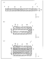
- (A) is a top view of the antenna device in a deployed state.
- (B) is a top view of the antenna device in a folded state.
- (A) is sectional drawing of the antenna apparatus of the unfolded state,
- (b) is sectional drawing of the antenna apparatus of the folded state,
- (c) is the antenna apparatus of the folded state It is other sectional drawing of.
- (A) is a perspective view of the 1st antenna of the folded state.
- (B) is a perspective view of the 2nd antenna of the folded state.
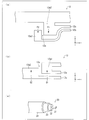
- (A) is a top view of the feeding portion of the first antenna.
- (B) is a top view of the feeding portion of the second antenna.
- (C) is a perspective view of the coaxial cable connected to these electric power feeding parts.
- FIG. 6 is a graph showing VSWR characteristics of the antenna device shown in FIG. 5.
- A is a graph which shows the efficiency (three-dimensional radiation efficiency) in the WWAN band (low frequency side band and intermediate band) of the antenna apparatus shown in FIG.
- B is a graph which shows the efficiency (three-dimensional radiation efficiency) in the WLAN band (high frequency side band) of the antenna apparatus shown in FIG.
- a thick line indicates the gain in the expanded state
- a thin line indicates the gain in the folded state.
- antenna device structure The structure of the antenna device 1 will be described with reference to FIG.
- FIG. 1A is a top view of the antenna device 1 in a deployed state
- FIG. 1B is a top view of the antenna device 1 in a folded state.
- the antenna device according to the present embodiment is the antenna device 1 in a folded state shown in FIG.
- the unfolded antenna device 1 shown in FIG. 1A is an intermediate product obtained in the process of manufacturing the antenna device according to this embodiment. Note that “folding along the straight line L” means “folding so that the straight line L becomes a ridgeline”.
- the antenna device 1 has three operation bands and includes two antennas 12 to 13.
- the first antenna 12 operates in two bands on the low frequency side among the three operating bands of the antenna device 1.
- the second antenna 13 operates in one band on the high frequency side among the three operating bands of the antenna device 1.
- the three operating bands of the antenna device 1 are (1) 824 MHz to 925 MHz (hereinafter referred to as “low frequency side band”), (2) 1920 to 2170 MHz (hereinafter referred to as “intermediate band”), (3) 2412 MHz to 2484 MHz (hereinafter referred to as “high frequency side band”) is assumed.
- the low frequency side band and the intermediate band are bands for WWAN (wireless access), and the high frequency side band is a band for WLAN (wireless LAN).
- the antenna device 1 further includes two dielectric sheets 14.
- Each of the first antenna 12 and the second antenna 13 is a thin-film conductor (specifically metal, more specifically copper or aluminum) formed by stamping, etching, pressing, or the like, It is sandwiched between these two dielectric sheets 14.
- the cross-sectional structure of the antenna device 1 will be described later with reference to another drawing.
- the first antenna 12 is an inverted F-type monopole antenna, and as shown in FIG. 1A, (1) a linear portion 12a1 extending in the positive y-axis direction from the feeding point P1, and (2) a linear portion 12a1.
- a linear portion 12b extending in the x-axis positive direction from the end opposite to the feeding point P1 side, and (3) a linear portion 12c extending in the x-axis negative direction from the end opposite to the feeding point P1 side of the linear portion 12a1.
- (4) a straight line portion 12a2 extending in the y-axis negative direction from the feeding point P2, and (5) a short-circuit portion 12d that short-circuits the straight line portion 12a1 and the straight line portion 12a2.
- the straight line portion 12a2 is disposed so as to face the straight line portion 12a1, and constitutes the power feeding portion 12a together with the straight line portion 12a1. The details of the structure of the power feeding unit 12a will be described later with reference to another drawing.
- the straight portion 12a1, the straight portion 12b, and the straight portion 12c function as radiating elements of the inverted F-type monopole antenna.
- the length Lb of the straight line portion 12b is set so that the sum La1 + Lb with the length La1 of the straight line portion 12a1 substantially matches c / (4fmid) so that resonance occurs in the intermediate band.
- c is the speed of light
- fmid is the center frequency of the intermediate band.
- the length Lc of the straight line portion 12c is set so that the sum La1 + Lc of the length with the straight line portion 12a1 substantially coincides with c / (4low) so that resonance occurs in the low frequency side band.
- c is the speed of light
- flow is the center frequency in the low frequency side band.
- the straight portion 12b and / or the straight portion 12c may be bent to form a mendder.
- the straight portion 12a2 functions as a part of the ground plane of the inverted F monopole antenna.
- an outer conductor of a coaxial cable is connected to the straight line portion 12a2.
- the coaxial cable is wired along with a metal part (for example, a metal frame of a display) mounted on a wireless device (for example, a portable information terminal) together with the antenna device 1.
- the metal component mounted on the wireless device together with the antenna device 1 also functions as a ground plane of the inverted F monopole antenna.
- the antenna device 1 can be significantly reduced in size.
- the short-circuit portion 12d short-circuits the two straight portions 12a1 to 12a2 constituting the power supply portion 12a, thereby connecting the coaxial cable connected to the power supply points P1 to P2 and the first antenna 12. It is the structure for aiming at impedance matching between.
- the coaxial cable is usually either 50 ⁇ series or 75 ⁇ series.
- the short-circuit portion 12d includes (1) a straight portion 12d1 extending in the positive x-axis direction from the end of the straight portion 12a2 opposite to the feeding point Q2, and (2) abbreviated.
- a bent portion 12d2 bent in an S-shape, one end of which is connected to the end of the straight portion 12d1 opposite to the straight portion 12a2 side; and (3) a straight portion of the bent portion 12d2.
- a linear portion 12d3 extending in the positive x-axis direction from the end opposite to the 12d1 side; and (4) a linear portion 12d4 extending in the positive y-axis direction from the end opposite to the bent portion 12d2 side of the linear portion 12d3.
- the linear portion 12d4 can be constituted by a linear portion 12d5 extending in the negative x-axis direction from the opposite end of the linear portion 12d3.
- the end of the straight portion 12d5 opposite to the straight portion 12d4 is connected to the end of the straight portion 12a1 on the feeding point P1 side, thereby short-circuiting the two straight portions 12a1 to 12a2 constituting the feeding portion 12a. A short circuit is formed.
- the short-circuit portion 12d is arranged on the linear portion 12b side from the straight portion 12a1. As a result, it is possible to avoid a decrease in gain and a narrowing of the operating band that may occur when the short-circuit portion 12d is arranged closer to the straight portion 12c than the straight portion 12a1.
- a rectangular notch 12b1 extending in the longitudinal direction (x-axis direction) of the linear portion 12b from the end opposite to the linear portion 12a side (the linear portion 12b). Is formed.
- a rectangular notch 12c1 extending in the longitudinal direction (x-axis direction) of the linear portion 12c from the end opposite to the linear portion 12a side (the linear portion 12c). Is formed.
- Such notches 12b1 to 12c1 can widen the bandwidth of the intermediate band and the low frequency side band.
- the depth of the notch 12b is 5 mm or less.
- the depth of the notch 12c1 is preferably 10 mm or less.
- a rectangular opening (slot) 12c2 extending in the longitudinal direction (the x-axis direction) of the linear portion 12c is formed in the linear portion 12c.
- the second antenna 13 is an inverted F-type monopole antenna, and as shown in FIG. 1A, (1) a linear portion 13a1 extending in the positive y-axis direction from the feeding point Q1, and (2) a linear portion 13a1.
- a straight portion 13b1 extending in the x-axis positive direction from the end opposite to the feeding point Q1 side, and (3) a straight portion 13b2 extending in the y-axis positive direction from the end opposite to the straight portion 13a1 side of the straight portion 13b1.
- a straight line portion 13b3 extending in the negative x-axis direction from the end of the straight line portion 13b2 opposite to the straight line portion 13b1, and (5) a straight line portion 13a2 extending in the negative y-axis direction from the feeding point Q2.
- the straight line portion 13a2 is disposed so as to face the straight line portion 13a1, and constitutes the power feeding portion 13a together with the straight line portion 13a1. Note that details of the structure of the power supply unit 13a will be described later with reference to another drawing.
- the straight portion 13a1 and the straight portions 13b1 to 13b3 function as radiating elements of the inverted F-type monopole antenna.
- the lengths L′ b1 to L′ b3 of the straight portions 13b1 to 13b3 are approximately equal to the sum L′ a1 + L′ b1 + L′ b2 + L′ b3 with the length L′ a1 of the straight portion 13a so that resonance occurs in the high frequency side band.
- / (4fhigh) is set to match.
- c is the speed of light
- fhigh is the center frequency of the high frequency side band.
- the straight portion 13a2 functions as a part of the ground plane of the inverted F-type monopole antenna.
- an outer conductor of a coaxial cable is connected to the straight line portion 13a2.
- the coaxial cable is wired along with a metal part (for example, a metal frame of a display) mounted on a wireless device (for example, a portable information terminal) together with the antenna device 1.
- the metal component mounted on the wireless device together with the antenna device 1 also functions as a ground plane of the inverted F monopole antenna.
- the antenna device 1 can be significantly reduced in size.
- the short-circuit portion 13 c short-circuits the two straight portions 13 a 1 to 13 a 2 constituting the power feeding portion 12, thereby connecting the coaxial cable connected to the power feeding points Q 1 to Q 2 and the second antenna 13. It is the structure for aiming at impedance matching between.
- the short-circuit portion 13c includes: (1) a straight portion 13c1 extending in the positive direction of the x-axis from the end opposite to the feeding point Q2 side of the straight portion 13a2, and (2) a straight line.
- a straight portion 13c2 extending in the positive y-axis direction from the end of the portion 13c1 opposite to the straight portion 13a2, and (3) a straight line extending in the negative x-axis direction from the end of the straight portion 13c2 opposite to the straight portion 13c1. It can comprise by the part 13c3.
- the end portion of the straight line portion 13c3 on the straight line portion 13c2 side is connected to the end portion of the straight line portion 13a1 on the power feeding point Q1 side, whereby a short circuit that short-circuits the two straight line portions 13a1 to 13a2 constituting the power feeding portion 13a. It is formed.
- a rectangular opening (slot) 13b4 extending in the longitudinal direction is formed in the straight line portion 13b3.
- the straight portions 12b to 12c in the first antenna 12 and the straight portion 13b3 in the second antenna 13 have a central axis extending in the longitudinal direction thereof (the straight portions 12b to 12c and the straight portion 13b3) as a straight line L. They are arranged to match. Therefore, when the antenna device 1 is folded along the straight line L, the straight portions 12b to 12c and the straight portion 13b3 are folded along the central axis extending in the longitudinal direction thereof. Thereby, the width (width in the folded state) of the mounted product can be halved while maintaining the width (width in the unfolded state) of the straight portions 12b to 12c and the straight portion 13b3 as the conductor. it can. That is, it is possible to reduce the size while maintaining a wide operating band.
- FIG. 2 (a) is a cross-sectional view taken along the line AA ′ (see FIG. 1 (a)) of the antenna device 1 in the unfolded state
- FIGS. 2 (b) to 2 (c) are respectively
- FIG. 2 is a cross-sectional view taken along the line AA ′ in the folded antenna device 1 (see FIG. 1B).
- FIG. 3A is a perspective view of a portion where the first antenna 12 is arranged in the antenna device 1 in a folded state
- FIG. 3B is an antenna device in a folded state.
- 1 is a perspective view of a portion in which a second antenna 13 is disposed.
- the deployed antenna device 1 has a cross-sectional structure in which the antenna 12 is sandwiched between two dielectric sheets 14a to 14b, as shown in FIG. 2 (a).
- the two dielectric sheets 14a to 14b and the antenna 12 are bonded to each other with an adhesive 15, for example.
- Each of the two dielectric sheets 14a to 14b may be made of a flexible material such as polyimide or polyethylene.
- the antenna device 1 in the folded state is folded in two. To obtain.
- FIG. 2 (b) a configuration in which the inward surfaces of the dielectric sheet 14b (the surface opposite to the surface on the side of the radiating element 12) are bonded together by the adhesive 16
- FIG. 2C a configuration may be adopted in which the dielectric substrate 17 is sandwiched between the dielectric sheets 14 b and the inward surface of the dielectric sheet 14 b is bonded to the dielectric substrate 17 with the adhesive 16.
- the characteristics of the antenna 12 can be adjusted by changing the dielectric constant of the adhesive 16.
- the characteristics of the antenna 12 can be adjusted by changing the dielectric constant of the dielectric substrate 17.
- the dielectric substrate 17 can prevent warping of the antenna device 1 and increase the strength of the antenna device 1.
- a portion covering the straight portions 12a1 to 12a2 constituting the power feeding portion 12 is peeled off, and solder 18 is injected into the portion.
- the portions in contact with the solder 18 serve as feeding points P 1 to P 2 for supplying a high frequency current to the antenna 12.
- 2 and 3 are schematic views for explaining the cross-sectional structure of the antenna device 1, and do not limit the dimensions of each part.
- 2 and 3 show a configuration in which the antenna device 1 in a deployed state is bent into a U shape with two straight lines parallel to the straight line L as ridge lines.
- the present invention is not limited to this. is not.
- the inward surfaces of the dielectric sheet 14b are in close contact with each other, and the thickness of the antenna device 1 in the folded state is approximately twice the thickness of the antenna device 1 in the unfolded state.
- the thickness of the dielectric sheets 14a to 14b is 0.025 mm and the thickness of the adhesive (layers) 15 to 16 is 0.03 mm
- the thickness of the folded antenna device 1 is 0.19 mm.
- the thickness of the dielectric sheets 14a to 14b is 0.025 mm
- the thickness of the adhesives (layers) 15 to 16 is 0.03 mm
- the dielectric When the thickness of the body substrate 17 is 0.3 mm, the thickness of the antenna device 1 in the folded state is 0.52 mm.
- the thickness of the antenna 12 (radiating element portion) is the same as the thickness of the adhesive (layer) 15, but the antenna 12 (radiating element portion).
- the actual thickness of the antenna 12 is as thin as 0.009 mm, and the antenna 12 (radiating element portion thereof) is embedded in the adhesive (layer) 15. Therefore, the thickness of the antenna 12 (radiating element portion thereof) does not contribute to the thickness of the antenna device 1 in the folded state.
- the antenna device 1 obtained by folding the antennas 12 to 13 sandwiched between the two dielectric sheets 14a to 14b in two is described.
- the present invention is not limited to this. That is, a multi-fold antenna device such as an antenna device obtained by folding an antenna sandwiched between two dielectric sheets in three or an antenna device obtained by folding in four is also included in the scope of the present invention.
- FIG. 4A is a top view of the power feeding unit 12a
- FIG. 4B is a top view of the power feeding unit 13a
- FIG. 4C is a perspective view of a coaxial cable connected to the power feeding unit 12a and the power feeding unit 13a.
- the feeding portion 12a of the first antenna 12 is composed of two linear portions 12a1 to 12a2 facing each other.
- the straight portion 12a1 is provided with a feeding point P1 to which the inner conductor 21 of the coaxial cable 20 is connected
- the straight portion 12a2 is provided with a feeding point P2 to which the outer conductor 23 of the coaxial cable 20 is connected.
- the coaxial cable 20 is drawn out from the feeding unit 12a in the negative x-axis direction. Since the short-circuit portion 12d is drawn from the power supply portion 12a in the positive x-axis direction, the coaxial cable 20 and the short-circuit portion 12d are drawn from the power supply portion 12a in opposite directions. Thereby, the influence which the routing (arrangement) of the coaxial cable 20 has on the antenna characteristics can be reduced. That is, even when the coaxial cable 20 is not fixed, the characteristics of the antenna 12 can be stabilized.
- the power feeding portion 13a of the second antenna 13 is composed of two linear portions 13a1 to 13a2 facing each other.
- the straight line portion 13a1 is provided with a feeding point Q1 to which the inner conductor 21 of the coaxial cable 20 (a coaxial cable different from the coaxial cable connected to the power feeding portion 12a) is connected, and the straight line portion 13a2 is provided with the coaxial cable 20 A feeding point Q2 to which the outer conductor 23 is connected is provided.
- the coaxial cable 20 is drawn out in the negative x-axis direction from the feeding portion 13a. Since the short-circuit portion 13c is drawn from the power supply portion 13a in the positive x-axis direction, the coaxial cable 20 and the short-circuit portion 13c are drawn from the power supply portion 13a in opposite directions. Thereby, the influence which the routing (arrangement) of the coaxial cable 20 has on the antenna characteristics can be reduced. That is, even when the coaxial cable 20 is not fixed, the characteristics of the antenna 13 can be stabilized.
- FIGS. 6 to 9 are characteristics of the antenna apparatus 1 shown in FIG. 5 folded.
- each part of the first antenna 12 included in the antenna device 1 shown in FIG. 5 are as follows.
- Short-circuit part 12d: Width Wd 0.5 mm
- Straight line portion 12d1: length Ld1 3.6 mm
- Straight line portion 12d3: length Ld3 14.1 mm
- Straight line portion 12d4: length Ld4 0.5 mm
- FIG. 6 is a graph showing the VSWR characteristics of the antenna device 1. From FIG. 6, the VSWR value in the low frequency side band is 3, the VSWR value in the intermediate band is less than 3, and the VSWR value in the high frequency side band is less than 2, indicating that the antenna device 1 has very good VSWR characteristics. I understand.
- FIG. 7A is a graph showing the efficiency (three-dimensional radiation efficiency) of the antenna device 1 in the WWAN band (low frequency side band and intermediate band). From FIG. 7 (a), the efficiency in the low frequency side band exceeds -2.3 dB, and the efficiency in the intermediate band exceeds -2.7 dB, satisfying the condition (-3.5 dB or more) defined in the standard. I understand that.
- FIG. 7B is a graph showing the efficiency (three-dimensional radiation efficiency) of the antenna device 1 in the WLAN band (high frequency side band). From FIG. 7B, it can be seen that the efficiency in the high frequency side band exceeds ⁇ 1.8 dB, which satisfies the condition ( ⁇ 2 dB or more) defined in the standard.
- FIG. 8 is a graph showing the gain of the antenna device 1 in the unfolded state and the folded state. As shown in FIG. 8, the gain of the antenna device 1 is lowered by folding the antenna device 1. However, even in the folded state, a gain of ⁇ 4 dB or more in all the operating bands ( ⁇ 4.5 dB or more in almost all the operating bands) is ensured, and the antenna device 1 is used even in the folded state. It turns out that it is possible.
- FIG. 9 is a graph showing the gain when the notches 12b1 and 12c2 are formed at the ends of the straight portion 12b and the straight portion 12c and the gain when the notches are not formed. From FIG. 9, by forming the notches 12b1 and 12c2 at the ends of the straight line portion 12b and the straight line portion 12c, the gain increases in the low frequency side band and the intermediate band, and in particular, the gain increases remarkably in the intermediate band. I understand.
- the antenna device includes the thin-film radiating element and the two dielectric sheets sandwiching the radiating element, and the radiation of one of the two dielectric sheets. It has a structure in which the radiating element and the two dielectric sheets are folded so that surfaces opposite to the element side face each other.
- the mounting area of the antenna device can be reduced without reducing the length and width of the radiating element as a conductor.
- the antenna device when the antenna device is manufactured, unlike the case where the antenna device described in Patent Document 1 is manufactured, a process of attaching a thin-film radiating element to the surface of the substrate is not required. Further, since the radiating element is sandwiched between the two dielectric sheets, the radiation and the two dielectric sheets can be folded without physically damaging the thin-film radiating element. . That is, manufacture is easy.
- the radiating element and the two dielectric sheets are folded along a straight line including a central axis of a linear portion constituting the radiating element.
- the size of the antenna device can be made more compact while maintaining the bandwidth of the antenna device.
- the radiating element and the two dielectric sheets include a central axis of a linear portion disposed at a position farthest from a feeding point among the linear portions constituting the radiating element. It is preferably folded in a straight line.
- the antenna device can be lowered in height by half the width of the straight line portion.
- the radiating element includes a first straight portion extending in the first direction from the feeding point, and a first linear portion from the end opposite to the feeding point side of the first straight portion.
- a second linear portion extending in a second direction orthogonal to the direction of the first linear portion, and a third linear portion extending in an opposite direction to the second direction from the end of the first linear portion on the opposite side to the power feeding portion side.
- the radiating element and the two dielectric sheets are folded along a straight line including a central axis of the second straight part and a central axis of the third straight line.
- the antenna device can be operated in at least two bands.
- the tip of the second radiating element has a notch extending from the tip in the direction opposite to the second direction, or the tip of the third radiating element. It is preferable that a notch extending from the tip in the second direction is formed.
- the bandwidth of at least one of the two bands can be expanded.
- the length of the third straight line portion is longer than the length of the second straight line portion, and the fourth straight line portion and the first straight line that form a feeding portion together with the first straight line portion. It is preferable that the short circuit part which short-circuits a part is arrange
- another radiating element in the form of a thin film is sandwiched between the two dielectric sheets, and the other radiating element extends in the first direction from the feeding point.
- a fifth straight portion extending, a sixth straight portion extending in the second direction from an end opposite to the feeding point side of the fifth straight portion, and the fifth straight portion side of the sixth straight portion.
- the radiating element and the two dielectric sheets include a straight line including a central axis of the second straight part, a central axis of the third straight part, and a central axis of the eighth straight part. It is preferable that it is folded by.
- the antenna device can be operated in at least three bands in total.
- the manufacturing method according to the present embodiment is a method for manufacturing an antenna device including a thin-film radiating element and two dielectric sheets sandwiching the radiating element, and one of the two dielectric sheets. A step of folding the radiating element and the two dielectric sheets so that surfaces opposite to the radiating element side face each other.
- an antenna device having a small mounting area can be easily manufactured without reducing the length and width of the radiating element as a conductor.
- the antenna device of the present invention can be suitably used as an antenna device mounted on a small wireless device.
- it can be suitably used as an antenna device mounted on a mobile phone terminal, a smartphone, a PDA, an electronic book reader, or the like.
Landscapes
- Engineering & Computer Science (AREA)
- Computer Networks & Wireless Communication (AREA)
- Details Of Aerials (AREA)
- Support Of Aerials (AREA)
Abstract
アンテナ装置(1)は、アンテナ(12)と、アンテナ(12)を挟み込む2枚の誘電体シート(14)とを備えている。アンテナ装置(1)は、一方の誘電体シート(14)のアンテナ(12)側と反対側の面同士が互いに対向するよう、直線Lでアンテナ(12)及び誘電体シート(14)を折畳んだ構造を有している。
Description
本発明は、薄膜状の放射素子を有するアンテナ装置に関する。また、そのようなアンテナ装置の製造方法に関する。
アンテナ装置を薄型化するために、薄膜状の放射素子を有するアンテナ装置が広く用いられている。このようなアンテナ装置は、普及の著しい小型無線装置、例えば携帯電話端末、スマートフォン、PDA、電子ブックリーダ等において、欠くことのできないデバイスになりつつある。
このようなアンテナ装置は、通常、2枚の誘電体シートの間に薄膜状の放射素子を挟み込んだ構造を有している。また、特許文献1に記載のように、誘電体である基体の表面に薄膜状の放射素子を貼付けた構造も知られている。
しかしながら、2枚の誘電体シートの間に薄膜状の放射素子を挟み込む構造を採用した場合、アンテナ装置の実装面積が大きくなり、小型無線装置への搭載が困難になるという問題があった。特に、広帯域化を実現するためには、放射素子の長さを長くしたり放射素子の幅を広くしたりする必要がある。しかしながら、放射素子の長さを長くしたり放射素子の幅を広くしたりするほど、この問題は深刻になる。
また、特許文献1に記載のように、誘電体である基体の表面に薄膜状の放射素子を貼付ける構造を採用した場合、アンテナ装置の厚み大きくなり、小型無線装置への実装が困難になるという問題があった。また、このような構造を採用したアンテナ装置を製造する場合、薄膜状の放射素子を基体の表面に貼付ける工程が必要となる。しかしながら、薄膜状の放射素子に物理的損傷を与えることなくこの工程を実行するのは容易ではなく、その結果、製造コストの上昇を免れないという問題があった。
本発明は上記の課題に鑑みてなされたものであり、薄膜状の放射素子を有するアンテナ装置において、製造が容易でありながら実装面積の小さいアンテナ装置を実現することにある。
上記課題を解決するために、本発明に係るアンテナ装置は、薄膜状の放射素子と、上記放射素子を挟み込む2枚の誘電体シートとを備え、上記2枚の誘電体シートの何れか一方の上記放射素子側と反対側の面同士が互いに対向するように、上記放射素子及び上記2枚の誘電体シートを折畳んだ構造を有している、ことを特徴とする。
上記の構成によれば、上記放射素子の導体としての長さ及び幅を小さくすることなく、上記アンテナ装置の実装面積を小さくすることができる。
また、上記アンテナ装置を製造する場合、特許文献1に記載のアンテナ装置を製造する場合のように、薄膜状の放射素子を基体の表面に貼り付ける工程を要さない。また、上記放射素子は上記2枚の誘電体シートに挟み込まれているため、薄膜状の放射素子に物理的損傷を与えることなく、上記放射及び上記2枚の誘電体シートを折畳むことができる。すなわち、製造が容易である。
また、上記課題を解決するために、本発明に係るアンテナ装置の製造方法は、薄膜状の放射素子を2枚の誘電体シートで挟み込む工程と、上記2枚の誘電体シートの何れか一方の上記放射素子側と反対側の面同士が互いに対向するように、上記放射素子及び上記2枚の誘電体シートを折畳む工程を含んでいる、ことを特徴とする。
上記の構成によれば、放射素子の導体としての長さ及び幅を小さくすることなく、実装面積を小さくしたアンテナ装置を、容易に製造することができる。
本発明によれば、製造が容易でありながら実装面積の小さいアンテナ装置を実現することができる。
本発明の一実施形態に係るアンテナ装置について、図面に基づいて説明すれば以下のとおりである。
〔アンテナ装置の構造〕
アンテナ装置1の構造について、図1を参照して説明する。
アンテナ装置1の構造について、図1を参照して説明する。
図1(a)は、展開された状態のアンテナ装置1の上面図であり、図1(b)は、折畳まれた状態のアンテナ装置1の上面図である。図1(a)に示すアンテナ装置1を直線Lで折畳むと、図1(b)に示すアンテナ装置1が得られる。本実施形態に係るアンテナ装置は、図1(b)に示す折畳まれた状態のアンテナ装置1である。図1(a)に示す展開された状態のアンテナ装置1は、本実施形態に係るアンテナ装置を製造する過程で得られる中間生成物である。なお、「直線Lで折畳む」とは、「直線Lが稜線となるように折畳む」ことを指す。
アンテナ装置1は、3つの動作帯域を有するものであり、2つのアンテナ12~13を備えている。第1のアンテナ12は、アンテナ装置1の3つの動作帯域のうち、低周波側の2つの帯域で動作する。一方、第2のアンテナ13は、アンテナ装置1の3つの動作帯域のうち、高周波側の1つの帯域で動作する。本実施形態においては、アンテナ装置1の3つの動作帯域として、(1)824MHz~925MHz(以下「低周波側帯域」と記載)、(2)1920~2170MHz(以下「中間帯域」と記載)、及び、(3)2412MHz~2484MHz(以下「高周波側帯域」と記載)を想定する。低周波側帯域及び中間帯域は、WWAN(無線アクセス)用の帯域であり、高周波側帯域は、WLAN(無線LAN)用の帯域である。
アンテナ装置1は、更に、2枚の誘電体シート14を備えている。第1のアンテナ12及び第2のアンテナ13は、それぞれ、打ち抜き、エッチング、又はプレス加工等により形成された薄膜状の導体(具体的には金属、より具体的には銅又はアルミニウム)であり、これら2枚の誘電体シート14の間に挟み込まれている。なお、アンテナ装置1の断面構造については、参照する図面を代えて後述する。
第1のアンテナ12は、逆F型モノポールアンテナであり、図1(a)に示すように、(1)給電点P1からy軸正方向に伸びる直線部12a1と、(2)直線部12a1の給電点P1側と反対側の端部からx軸正方向に伸びる直線部12bと、(3)直線部12a1の給電点P1側と反対側の端部からx軸負方向に伸びる直線部12cと、(4)給電点P2からy軸負方向に伸びる直線部12a2と、(5)直線部12a1と直線部12a2とを短絡する短絡部12dとにより構成される。直線部12a2は、直線部12a1と互いに対向するように配置され、直線部12a1と共に給電部12aを構成する。なお、給電部12aの構造の詳細については、参照する図面を代えて後述する。
第1のアンテナ12において、直線部12a1、直線部12b、及び直線部12cは、逆F型モノポールアンテナの放射素子として機能する。中間帯域において共振が生じるよう、直線部12bの長さLbは、直線部12a1の長さLa1との和La1+Lbが概ねc/(4fmid)に一致するように設定される。ここで、cは光速であり、fmidは中間帯域の中心周波数である。また、低周波側帯域において共振が生じるよう、直線部12cの長さLcは、直線部12a1との長さの和La1+Lcが概ねc/(4flow)に一致するように設定される。ここで、cは光速であり、flowは低周波側帯域内の中心周波数である。なお、動作帯域を変えずにアンテナ12のサイズ(特にx軸方向のサイズ)を小さくするために、直線部12b及び/又は直線部12cを折り曲げて、メンアダ化してもよい。
第1のアンテナ12において、直線部12a2は、逆F型モノポールアンテナの地板の一部として機能する。直線部12a2には、後述するように、同軸ケーブルの外側導体が接続される。この同軸ケーブルは、アンテナ装置1と共に無線機器(例えば携帯型情報端末)に搭載された金属部品(例えばディスプレイの金属フレーム)に沿って配線される。これにより、アンテナ装置1と共に無線機器に搭載された金属部品も、逆F型モノポールアンテナの地板として機能する。このように、アンテナ装置1と共に搭載された金属部品を直線部12a2と共に地板として利用することによって、アンテナ装置1の大幅な小型化が実現される。
第1のアンテナ12において、短絡部12dは、給電部12aを構成する2つの直線部12a1~12a2を短絡することによって、給電点P1~P2に接続される同軸ケーブルと第1のアンテナ12との間のインピーダンス整合を図るための構成である。なお、同軸ケーブルは、通常、50Ω系列か75Ω系列かの何れかである。
短絡部12dは、例えば、図1(a)に示すように、(1)直線部12a2の給電点Q2側と反対側の端部からx軸正方向に伸びる直線部12d1と、(2)略S字状に屈曲した屈曲部12d2であって、一方の端部が直線部12d1の直線部12a2側と反対側の端部に接続された屈曲部12d2と、(3)屈曲部12d2の直線部12d1側と反対側の端部からx軸正方向に伸びる直線部12d3と、(4)直線部12d3の屈曲部12d2側と反対側の端部からy軸正方向に伸びる直線部12d4と、(5)直線部12d4の直線部12d3側と反対側の端部からx軸負方向に伸びる直線部12d5とにより構成することができる。直線部12d5の直線部12d4側と反対側の端部は、直線部12a1の給電点P1側の端部に接続され、これにより、給電部12aを構成する2つの直線部12a1~12a2を短絡する短絡路が形成される。
なお、本実施形態に係るアンテナ装置1においては、短絡部12dを直線部12a1より直線部12b側に配置している。これにより、短絡部12dを直線部12a1より直線部12c側に配置した場合に生じ得る低周波側帯域における利得の低下及び動作帯域の狭小化を回避することができる。
また、本実施形態に係るアンテナ装置1においては、直線部12bに、直線部12a側と反対側の端辺からその(直線部12bの)長手方向(x軸方向)に伸びる矩形状の切欠12b1が形成されている。また、本実施形態に係るアンテナ装置1においては、直線部12cに、直線部12a側と反対側の端辺からその(直線部12cの)長手方向(x軸方向)に伸びる矩形状の切欠12c1が形成されている。このような切欠12b1~12c1によって、中間帯域及び低周波側帯域の帯域幅を広げることができる。なぜなら、直線部12b~12c内に長さの異なる複数の電流路が生じ、その結果、これら複数の電流路の各々に対応する共振周波数が生じるためである。また、これらの切欠12b1~12c1を形成することによって、中間帯域及び低周波側帯域における利得を上げることができる。この事実を実証する実験結果については後述する。
なお、切欠12b1を深くするほど、中間帯域の帯域幅は広がるが、同時に、中間帯域内にヌル点が現れたり、切欠12b1を起点とするクラックにより直線部12bが断裂し易くなったりする。このため、切欠12bの深さは、5mm以下であることが好ましい。同様の理由により、切欠12c1の深さは、10mm以下であることが好ましい。
また、本実施形態に係るアンテナ装置1においては、直線部12cに、その(直線部12cの)長手方向(x軸方向)に伸びる矩形状の開口(スロット)12c2が形成されている。このような開口12c2を形成することによって、直線部12cにクラックが発生することを防止できる。
第2のアンテナ13は、逆F型モノポールアンテナであり、図1(a)に示すように、(1)給電点Q1からy軸正方向に伸びる直線部13a1と、(2)直線部13a1の給電点Q1側と反対側の端部からx軸正方向に伸びる直線部13b1と、(3)直線部13b1の直線部13a1側と反対側の端部からy軸正方向に伸びる直線部13b2と、(4)直線部13b2の直線部13b1側と反対側の端部からx軸負方向に伸びる直線部13b3と、(5)給電点Q2からy軸負方向に伸びる直線部13a2と、(6)直線部13a1と直線部13a2とを短絡する短絡部13cとにより構成される。ここで、直線部13a2は、直線部13a1と互いに対向するように配置され、直線部13a1と共に給電部13aを構成する。なお、給電部13aの構造の詳細については、参照する図面を代えて後述する。
第2のアンテナ13において、直線部13a1及び直線部13b1~13b3は、逆F型モノポールアンテナの放射素子として機能する。高周波側帯域において共振が生じるよう、直線部13b1~13b3の長さL’b1~L’b3は、直線部13aの長さL’a1との和L’a1+L’b1+L’b2+L’b3が概ねc/(4fhigh)に一致するように設定される。ここで、cは光速であり、fhighは高周波側帯域の中心周波数である。
第2のアンテナ13において、直線部13a2は、逆F型モノポールアンテナの地板の一部として機能する。直線部13a2には、後述するように、同軸ケーブルの外側導体が接続される。この同軸ケーブルは、アンテナ装置1と共に無線機器(例えば携帯型情報端末)に搭載された金属部品(例えばディスプレイの金属フレーム)に沿って配線される。これにより、アンテナ装置1と共に無線機器に搭載された金属部品も、逆F型モノポールアンテナの地板として機能する。このように、アンテナ装置1と共に搭載された金属部品を直線部13a2と共に地板として利用することによって、アンテナ装置1の大幅な小型化が実現される。
第2のアンテナ13において、短絡部13cは、給電部12を構成する2つの直線部13a1~13a2を短絡することによって、給電点Q1~Q2に接続される同軸ケーブルと第2のアンテナ13との間のインピーダンス整合を図るための構成である。
短絡部13cは、例えば、図1(a)に示すように、(1)直線部13a2の給電点Q2側と反対側の端部からx軸正方向に伸びる直線部13c1と、(2)直線部13c1の直線部13a2側と反対側の端部からy軸正方向に伸びる直線部13c2と、(3)直線部13c2の直線部13c1側と反対側の端部からx軸負方向に伸びる直線部13c3とにより構成することができる。直線部13c3の直線部13c2側の端部は、直線部13a1の給電点Q1側の端部に接続され、これにより、給電部13aを構成する2つの直線部13a1~13a2を短絡する短絡路が形成される。
なお、本実施形態に係るアンテナ装置1においては、直線部13b3に、その長手方向に伸びる矩形状の開口(スロット)13b4が形成されている。このような開口13b4を形成することによって、直線部13b3にクラックが発生することを防止できる。
なお、第1のアンテナ12における直線部12b~12c、及び、第2のアンテナ13における直線部13b3は、それら(直線部12b~12c及び直線部13b3)の長手方向に伸びる中心軸が直線Lと一致するように配置されている。したがって、アンテナ装置1を直線Lで折畳むと、直線部12b~12c及び直線部13b3が、それらの長手方向に伸びる中心軸で折畳まれることになる。これにより、直線部12b~12c及び直線部13b3の導体としての幅(展開した状態での幅)を保ちながら、実装物としての幅(折畳まれた状態での幅)を半分にすることができる。すなわち、動作帯域の広さを保ちながら、コンパクト化を図ることができる。
〔アンテナ装置の断面構造〕
次に、アンテナ装置1の断面構造について、図2~図3を参照して説明する。
次に、アンテナ装置1の断面構造について、図2~図3を参照して説明する。
図2(a)は、展開された状態のアンテナ装置1におけるA-A’断面(図1(a)参照)の断面図であり、図2(b)~図2(c)は、それぞれ、折畳まれた状態のアンテナ装置1におけるA-A’断面(図1(b)参照)の断面図である。図3(a)は、折畳まれた状態のアンテナ装置1のうち、第1のアンテナ12が配置された部分の斜視図であり、図3(b)は、折畳まれた状態のアンテナ装置1のうち、第2のアンテナ13が配置された部分の斜視図である。
展開された状態のアンテナ装置1は、図2(a)に示すように、2枚の誘電体シート14a~14bの間にアンテナ12が挟みこまれた断面構造を有している。2枚の誘電体シート14a~14bとアンテナ12とは、例えば接着剤15によって互いに接着されている。2枚の誘電体シート14a~14bは、それぞれ、可撓性を有する材料、例えばポリイミドやポリエチレン等により構成するとよい。
折畳まれた状態のアンテナ装置1は、図2(b)及び図2(c)並びに図3(a)及び図3(b)に示すように、展開された状態のアンテナ装置1を2つ折にすることにより得られる。
この際、図2(b)に示すように、誘電体シート14bの内向面(放射素子12側の面と反対側の面)同士を接着剤16によって接着する構成を採用してもよいし、図2(c)に示すように、誘電体シート14bの間に誘電体基板17を挟み込み、誘電体シート14bの内向面を接着剤16によって誘電体基板17に接着する構成を採用してもよい。何れの構成においても、接着剤16の誘電率を変化させることによって、アンテナ12の特性を調整することができる。更に、後者の構成においては、誘電体基板17の誘電率を変化させることによっても、アンテナ12の特性を調整することができる。また、後者の構成においては、誘電体基板17によって、アンテナ装置1の反りを防止し、アンテナ装置1の強度を高めることができる。
また、誘電体シート14aにおいては、給電部12を構成する直線部12a1~12a2を覆う部分が剥ぎ取られ、当該部分に半田18が注入される。直線部12a1~12a2において、この半田18に接触する部分が、アンテナ12に高周波電流を供給するための給電点P1~P2となる。
なお、図2及び図3は、アンテナ装置1の断面構造を説明するための模式的なものであり、各部の寸法を限定するものではない。また、図2及び図3においては、展開された状態のアンテナ装置1を、直線Lに平行な2本の直線を稜線としてU字状に折り曲げる構成を示しているが、これに限定されるものではない。例えば、展開された状態のアンテナ装置1を、直線Lを稜線としてV字状に折り曲げる構成を採用してもよい。後者の構成の場合、誘電体シート14bの内向面同士が互いに密着し、折畳まれた状態のアンテナ装置1の厚みは、展開された状態のアンテナ装置1の厚みの約2倍になる。
前者の構成において、図2(b)に示す断面構造を採用した場合、誘電体シート14a~14bの厚みを0.025mm、接着剤(層)15~16の厚みを0.03mmとすると、折畳まれた状態のアンテナ装置1の厚みは、0.19mmとなる。また、前者の構成において、図2(c)に示す断面構造を採用した場合、誘電体シート14a~14bの厚みを0.025mm、接着剤(層)15~16の厚みを0.03mm、誘電体基板17の厚みを0.3mmとすると、折畳まれた状態のアンテナ装置1の厚みは、0.52mmとなる。なお、図2(b)及び図2(c)においては、アンテナ12(の放射素子部分)の厚みを接着剤(層)15の厚みと同じにしているが、アンテナ12(の放射素子部分)の実際の厚みは0.009mmと薄く、アンテナ12(の放射素子部分)は接着剤(層)15に埋設される。したがって、アンテナ12(の放射素子部分)の厚みは、折畳まれた状態のアンテナ装置1の厚みに寄与しない。
なお、本実施形態においては、2枚の誘電体シート14a~14bに挟まれたアンテナ12~13を2つ折にして得られるアンテナ装置1について説明したが、これに限定されるものではない。すなわち、2枚の誘電体シートに挟まれたアンテナを3つ折にして得られるアンテナ装置や4つ折にして得られるアンテナ装置など多重折のアンテナ装置も本発明の範疇に含まれる。
〔アンテナ装置の給電部の構造〕
次に、第1のアンテナ12の給電部12a及び第2のアンテナ13の給電部13aについて、図4を参照して説明する。図4(a)は、給電部12aの上面図であり、図4(b)は、給電部13aの上面図である。また、図4(c)は、給電部12a及び給電部13aに接続される同軸ケーブルの斜視図である。
次に、第1のアンテナ12の給電部12a及び第2のアンテナ13の給電部13aについて、図4を参照して説明する。図4(a)は、給電部12aの上面図であり、図4(b)は、給電部13aの上面図である。また、図4(c)は、給電部12a及び給電部13aに接続される同軸ケーブルの斜視図である。
図4(a)に示すように、第1のアンテナ12の給電部12aは、互いに対向する2つの直線部12a1~12a2により構成される。直線部12a1には、同軸ケーブル20の内部導体21が接続される給電点P1が設けられ、直線部12a2には、同軸ケーブル20の外部導体23が接続される給電点P2が設けられる。
これらの給電点P1~P2の配置から明らかなように、同軸ケーブル20は、給電部12aからx軸負方向に引き出される。短絡部12dは、給電部12aからx軸正方向に引き出されるので、同軸ケーブル20と短絡部12dとは、給電部12aから互いに反対向きに引き出されることになる。これにより、同軸ケーブル20の引き回し(配置)がアンテナ特性に与える影響を小さくすることができる。つまり、同軸ケーブル20が固定されていない場合でも、アンテナ12の特性を安定化させることができる。
図4(b)に示すように、第2のアンテナ13の給電部13aは、互いに対向する2つの直線部13a1~13a2により構成される。直線部13a1には、同軸ケーブル20(給電部12aに接続される同軸ケーブルとは別の同軸ケーブル)の内部導体21が接続される給電点Q1が設けられ、直線部13a2には、同軸ケーブル20の外部導体23が接続される給電点Q2が設けられる。
これらの給電点Q1~Q2の配置から明らかなように、同軸ケーブル20は、同軸ケーブル20は、給電部13aからx軸負方向に引き出される。短絡部13cは、給電部13aからx軸正方向に引き出されるので、同軸ケーブル20と短絡部13cとは、給電部13aから互いに反対方向に引き出されることになる。これにより、同軸ケーブル20の引き回し(配置)がアンテナ特性に与える影響を小さくすることができる。つまり、同軸ケーブル20が固定されていない場合でも、アンテナ13の特性を安定化させることができる。
〔アンテナ装置の特性〕
次に、アンテナ装置1の特性について、図5~図9を参照して説明する。図6~図9に示す特性は、図5に示すアンテナ装置1を折畳んだものの特性である。
次に、アンテナ装置1の特性について、図5~図9を参照して説明する。図6~図9に示す特性は、図5に示すアンテナ装置1を折畳んだものの特性である。
図5に示すアンテナ装置1が備える第1のアンテナ12の各部の寸法は以下のとおりである。
直線部12a1:幅Wa1= 2.0mm / 長さLa1= 6.5mm
直線部12a2:幅Wa2= 2.0mm / 長さLa2= 3.0mm
直線部12b :幅Wb = 3.0mm / 長さLb =18.0mm
直線部12c :幅Wc = 3.0mm / 長さLc =52.0mm
切欠12b1 :幅Wb1= 1.0mm / 長さLb1= 1.0mm
切欠12c1 :幅Wc1= 1.0mm / 長さLc1= 3.8mm
開口12c2 :幅Wc2= 1.0mm / 長さLc2=19.0mm
短絡部12d :幅Wd = 0.5mm
直線部12d1:長さLd1 = 3.6mm
直線部12d3:長さLd3 =14.1mm
直線部12d4:長さLd4 = 0.5mm
直線部12d5:長さLd5 =16.2mm
図5に示すアンテナ装置1が備える第2のアンテナ13の各部の寸法は以下のとおりである。
直線部12a2:幅Wa2= 2.0mm / 長さLa2= 3.0mm
直線部12b :幅Wb = 3.0mm / 長さLb =18.0mm
直線部12c :幅Wc = 3.0mm / 長さLc =52.0mm
切欠12b1 :幅Wb1= 1.0mm / 長さLb1= 1.0mm
切欠12c1 :幅Wc1= 1.0mm / 長さLc1= 3.8mm
開口12c2 :幅Wc2= 1.0mm / 長さLc2=19.0mm
短絡部12d :幅Wd = 0.5mm
直線部12d1:長さLd1 = 3.6mm
直線部12d3:長さLd3 =14.1mm
直線部12d4:長さLd4 = 0.5mm
直線部12d5:長さLd5 =16.2mm
図5に示すアンテナ装置1が備える第2のアンテナ13の各部の寸法は以下のとおりである。
直線部13a1:幅W’a1= 2.1mm / 長さL’a1=2.0mm
直線部13a2:幅W’a2= 3.3mm / 長さL’a2=2.1mm
直線部13b1:幅W’b1= 0.7mm / 長さL’b1=4.1mm
直線部13b2:幅W’b2= 2.0mm / 長さL’b2=3.2mm
直線部13b3:幅W’b3= 2.0mm / 長さL’b3=8.1mm
直線部13b4:幅W’b4= 1.0mm / 長さL’b4=6.7mm
短絡部13c :幅W’c = 0.5mm
直線部13c1:長さL’c1=6.7 mm
直線部13c2:長さL’c2=0.5 mm
直線部13c3:長さL’c3=4.1 mm
図6は、アンテナ装置1のVSWR特性を示すグラフである。図6から、低周波側帯域におけるVSWR値は3を、中間帯域におけるVSWR値は3を、高周波側帯域におけるVSWR値は2を下回っており、アンテナ装置1が極めて良好なVSWR特性を有することが分かる。
直線部13a2:幅W’a2= 3.3mm / 長さL’a2=2.1mm
直線部13b1:幅W’b1= 0.7mm / 長さL’b1=4.1mm
直線部13b2:幅W’b2= 2.0mm / 長さL’b2=3.2mm
直線部13b3:幅W’b3= 2.0mm / 長さL’b3=8.1mm
直線部13b4:幅W’b4= 1.0mm / 長さL’b4=6.7mm
短絡部13c :幅W’c = 0.5mm
直線部13c1:長さL’c1=6.7 mm
直線部13c2:長さL’c2=0.5 mm
直線部13c3:長さL’c3=4.1 mm
図6は、アンテナ装置1のVSWR特性を示すグラフである。図6から、低周波側帯域におけるVSWR値は3を、中間帯域におけるVSWR値は3を、高周波側帯域におけるVSWR値は2を下回っており、アンテナ装置1が極めて良好なVSWR特性を有することが分かる。
図7(a)は、WWAN帯域(低周波側帯域及び中間帯域)におけるアンテナ装置1の効率(3次元放射効率)を示すグラフである。図7(a)から、低周波側帯域における効率は-2.3dBを、中間帯域における効率は-2.7dBを上回っており、規格に定められた条件(-3.5dB以上)を充足することが分かる。
図7(b)は、WLAN帯域(高周波側帯域)におけるアンテナ装置1の効率(3次元放射効率)を示すグラフである。図7(b)から、高周波側帯域における効率は-1.8dBを上回っており、規格に定められた条件(-2dB以上)を充足することが分かる。
図8は、展開された状態及び折畳まれた状態におけるアンテナ装置1の利得を示すグラフである。図8に示すように、アンテナ装置1の利得は、アンテナ装置1を折畳むことによって低下する。ただし、折畳まれた状態においても、動作帯域の全てにおいて-4dB以上(動作帯域の殆ど全てにおいて-4.5dB以上)の利得が確保されており、アンテナ装置1が折畳まれた状態でも使用可能であることが分かる。
図9は、直線部12b及び直線部12cの先端に切欠12b1及び12c2を形成した場合の利得と、形成しなかった場合の利得を示すグラフである。図9から、直線部12b及び直線部12cの先端に切欠12b1及び12c2を形成することによって、低周波側帯域及び中間帯域において利得が上昇すること、特に、中間帯域において著しく利得が上昇することが分かる。
〔まとめ〕
以上のように、本実施形態に係るアンテナ装置は、薄膜状の放射素子と、上記放射素子を挟み込む2枚の誘電体シートとを備え、上記2枚の誘電体シートの何れか一方の上記放射素子側と反対側の面同士が互いに対向するように、上記放射素子及び上記2枚の誘電体シートを折畳んだ構造を有している、ことを特徴とする。
以上のように、本実施形態に係るアンテナ装置は、薄膜状の放射素子と、上記放射素子を挟み込む2枚の誘電体シートとを備え、上記2枚の誘電体シートの何れか一方の上記放射素子側と反対側の面同士が互いに対向するように、上記放射素子及び上記2枚の誘電体シートを折畳んだ構造を有している、ことを特徴とする。
上記の構成によれば、上記放射素子の導体としての長さ及び幅を小さくすることなく、上記アンテナ装置の実装面積を小さくすることができる。
また、上記アンテナ装置を製造する場合、特許文献1に記載のアンテナ装置を製造する場合のように、薄膜状の放射素子を基体の表面に貼り付ける工程を要さない。また、上記放射素子は上記2枚の誘電体シートに挟み込まれているため、薄膜状の放射素子に物理的損傷を与えることなく、上記放射及び上記2枚の誘電体シートを折畳むことができる。すなわち、製造が容易である。
本実施形態に係るアンテナ装置において、上記放射素子及び上記2枚の誘電体シートは、上記放射素子を構成する直線部の中心軸を含む直線で折畳まれている、ことが好ましい。
上記の構成によれば、上記直線部の導体としての幅を保ったまま、上記直線部の実装上の幅を半分にすることができる。したがって、上記アンテナ装置の帯域幅を保ったまま、上記アンテナ装置のサイズをよりコンパクトにすることができる。
本実施形態に係るアンテナ装置において、上記放射素子及び上記2枚の誘電体シートは、上記放射素子を構成する直線部のうち、給電点から最も遠い場所に配置された直線部の中心軸を含む直線で折畳まれている、ことが好ましい。
上記の構成によれば、給電点から最も遠い場所に配置された直線部の幅が半分になるので、当該直線部の幅の半分だけアンテナ装置を低姿勢化することができる。
本実施形態に係るアンテナ装置において、上記放射素子は、上記給電点から第1の方向に伸びる第1直線部と、上記第1直線部の上記給電点側と反対側の端部から上記第1の方向に直交する第2の方向に伸びる第2直線部と、上記第1直線部の上記給電部側と反対側の端部から上記第2の方向と反対方向に伸びる第3直線部とを含み、上記放射素子及び上記2枚の誘電体シートは、上記第2直線部の中心軸及び上記第3の直線の中心軸を含む直線で折畳まれている、ことが好ましい。
上記の構成によれば、少なくとも2つの帯域において、上記アンテナ装置を動作させることが可能になる。
本実施形態に係るアンテナ装置において、上記第2の放射素子の先端に、当該先端から上記第2の方向と反対方向に伸びる切欠が形成されているか、又は、上記第3の放射素子の先端に、当該先端から上記第2の方向に伸びる切欠が形成されている、ことが好ましい。
上記の構成によれば、上記2つの帯域の少なくとも何れかの帯域幅を拡大することができる。
本実施形態に係るアンテナ装置において、上記第3直線部の長さは、上記第2直線部の長さよりも長く、上記第1直線部と共に給電部を構成する第4直線部と上記第1直線部とを短絡する短絡部が、上記第1直線部よりも上記第2直線部側に配置されている、ことが好ましい。
上記の構成によれば、上記2つの帯域のうち、低周波側の帯域(上記第3の直線部の長さに対応する帯域)において生じえる利得の低下及び帯域の狭小化を回避することができる。
本実施形態に係るアンテナ装置において、上記2枚の誘電体シートの間には、薄膜状の他の放射素子が挟み込まれており、上記他の放射素子は、給電点から上記第1の方向に伸びる第5直線部と、上記第5直線部の上記給電点側と反対側の端部から上記第2の方向に伸びる第6直線部と、上記第6直線部の上記第5直線部側とは反対側の端部から上記第1の方向に伸びる第7直線部と、上記第7直線部の上記第6直線部側と反対側の端部から上記第2の方向の反対方向に伸びる第8直線部とを含み、上記放射素子及び上記2枚の誘電体シートは、上記第2直線部の中心軸、上記第3直線部の中心軸、及び上記第8直線部の中心軸を含む直線で折畳まれている、ことが好ましい。
上記の構成によれば、合計して少なくとも3つの帯域において、上記アンテナ装置を動作させること可能になる。
本実施形態に係る製造方法は、薄膜状の放射素子と上記放射素子を挟み込む2枚の誘電体シートとを備えたアンテナ装置の製造方法であって、上記2枚の誘電体シートの何れか一方の上記放射素子側と反対側の面同士が互いに対向するように、上記放射素子及び上記2枚の誘電体シートを折り畳む工程を含んでいる、ことを特徴とする。
上記の構成によれば、放射素子の導体としての長さ及び幅を小さくすることなく、実装面積を小さくしたアンテナ装置を、容易に製造することができる。
本発明のアンテナ装置は、小型無線機器に搭載するアンテナ装置として、好適に利用することができる。例えば、携帯電話端末、スマートフォン、PDA、電子ブックリーダ等に搭載するアンテナ装置として、好適に利用することができる。
1 アンテナ装置
12 第1のアンテナ
12a 給電部
P1,P2 給電点
12a1 直線部(第1直線部、放射素子)
12a2 直線部(第4直線部)
12b 直線部(第2直線部、放射素子)
12b1 切欠
12c 直線部(第3直線部、放射素子)
12c1 切欠
12c2 開口
12d 短絡部
13 第2のアンテナ
13a 給電部
Q1,Q2 給電点
13a1 直線部(第5の直線部、他の放射素子)
13a2 直線部
13b1 直線部(第6直線部、他の放射素子)
13b2 直線部(第7直線部、他の放射素子)
13b3 直線部(第8直線部、他の放射素子)
13b4 開口
13c 短絡部
14 2枚の誘電体シート
14a 誘電体シート
14b 誘電体シート
15、16 接着材
17 誘電体基板(誘電体層)
18 半田
12 第1のアンテナ
12a 給電部
P1,P2 給電点
12a1 直線部(第1直線部、放射素子)
12a2 直線部(第4直線部)
12b 直線部(第2直線部、放射素子)
12b1 切欠
12c 直線部(第3直線部、放射素子)
12c1 切欠
12c2 開口
12d 短絡部
13 第2のアンテナ
13a 給電部
Q1,Q2 給電点
13a1 直線部(第5の直線部、他の放射素子)
13a2 直線部
13b1 直線部(第6直線部、他の放射素子)
13b2 直線部(第7直線部、他の放射素子)
13b3 直線部(第8直線部、他の放射素子)
13b4 開口
13c 短絡部
14 2枚の誘電体シート
14a 誘電体シート
14b 誘電体シート
15、16 接着材
17 誘電体基板(誘電体層)
18 半田
Claims (8)
- 薄膜状の放射素子と、
上記放射素子を挟み込む2枚の誘電体シートとを備え、
上記2枚の誘電体シートの何れか一方の上記放射素子側と反対側の面同士が互いに対向するように、上記放射素子及び上記2枚の誘電体シートを折畳んだ構造を有している、ことを特徴とするアンテナ装置。 - 上記放射素子及び上記2枚の誘電体シートは、上記放射素子を構成する直線部の中心軸を含む直線で折畳まれている、ことを特徴とする請求項1に記載のアンテナ装置。
- 上記放射素子及び上記2枚の誘電体シートは、上記放射素子を構成する直線部のうち、給電点から最も遠い場所に配置された直線部の中心軸を含む直線で折畳まれている、ことを特徴とする請求項2に記載のアンテナ装置。
- 上記放射素子は、
上記給電点から第1の方向に伸びる第1直線部と、
上記第1直線部の上記給電点側と反対側の端部から上記第1の方向に直交する第2の方向に伸びる第2直線部と、
上記第1直線部の上記給電点側と反対側の端部から上記第2の方向と反対方向に伸びる第3直線部とを含み、
上記放射素子及び上記2枚の誘電体シートは、上記第2直線部の中心軸及び上記第3直線部の中心軸を含む直線で折畳まれている、ことを特徴とする請求項3に記載のアンテナ装置。 - 上記第2直線部の先端に上記第2の方向と反対方向に伸びる切欠が形成されているか、又は、上記第3直線部の先端に上記第2の方向に伸びる切欠が形成されている、ことを特徴とする請求項4に記載のアンテナ装置。
- 上記第3直線部の長さは、上記第2直線部の長さよりも長く、
上記第1直線部と共に給電部を構成する第4直線部と上記第1直線部とを短絡する短絡部が、上記第1直線部よりも上記第2直線部側に配置されている、ことを特徴とする請求項4又は5に記載のアンテナ装置。 - 上記2枚の誘電体シートの間には、薄膜状の他の放射素子が挟み込まれており、
上記他の放射素子は、
給電点から上記第1の方向に伸びる第5直線部と、
上記第5直線部の上記給電点側と反対側の端部から上記第2の方向に伸びる第6直線部と、
上記第6直線部の上記第5直線部側とは反対側の端部から上記第1の方向に伸びる第7直線部と、
上記第7直線部の上記第6直線部側と反対側の端部から上記第2の方向の反対方向に伸びる第8直線部とを含み、
上記放射素子及び上記2枚の誘電体シートは、上記第2直線部の中心軸、上記第3直線部の中心軸、及び上記第8直線部の中心軸を含む直線で折畳まれている、ことを特徴とする請求項4から6までの何れか一項に記載のアンテナ装置。 - 薄膜状の放射素子を2枚の誘電体シートで挟み込む工程と、
上記2枚の誘電体シートの何れか一方の上記放射素子側と反対側の面同士が互いに対向するように、上記放射素子及び上記2枚の誘電体シートを折り畳む工程を含んでいる、ことを特徴とするアンテナ装置の製造方法。
Priority Applications (1)
| Application Number | Priority Date | Filing Date | Title |
|---|---|---|---|
| JP2013507660A JPWO2012133508A1 (ja) | 2011-03-31 | 2012-03-28 | アンテナ装置及びその製造方法 |
Applications Claiming Priority (2)
| Application Number | Priority Date | Filing Date | Title |
|---|---|---|---|
| JP2011-080958 | 2011-03-31 | ||
| JP2011080958 | 2011-03-31 |
Publications (1)
| Publication Number | Publication Date |
|---|---|
| WO2012133508A1 true WO2012133508A1 (ja) | 2012-10-04 |
Family
ID=46931217
Family Applications (1)
| Application Number | Title | Priority Date | Filing Date |
|---|---|---|---|
| PCT/JP2012/058095 Ceased WO2012133508A1 (ja) | 2011-03-31 | 2012-03-28 | アンテナ装置及びその製造方法 |
Country Status (2)
| Country | Link |
|---|---|
| JP (1) | JPWO2012133508A1 (ja) |
| WO (1) | WO2012133508A1 (ja) |
Citations (3)
| Publication number | Priority date | Publication date | Assignee | Title |
|---|---|---|---|---|
| JP2007142895A (ja) * | 2005-11-18 | 2007-06-07 | Toshiba Corp | 無線装置および電子機器 |
| JP2007311935A (ja) * | 2006-05-16 | 2007-11-29 | Toshiba Corp | 平面アンテナ |
| JP2008167098A (ja) * | 2006-12-28 | 2008-07-17 | Nec Saitama Ltd | アンテナ装置及び該アンテナ装置を用いた携帯無線機 |
Family Cites Families (2)
| Publication number | Priority date | Publication date | Assignee | Title |
|---|---|---|---|---|
| TWI355610B (en) * | 2007-12-21 | 2012-01-01 | Ind Tech Res Inst | Anti-metal rf identification tag and the manufactu |
| JP5456598B2 (ja) * | 2010-06-25 | 2014-04-02 | 富士通株式会社 | 無線タグ、及びその製造方法 |
-
2012
- 2012-03-28 JP JP2013507660A patent/JPWO2012133508A1/ja active Pending
- 2012-03-28 WO PCT/JP2012/058095 patent/WO2012133508A1/ja not_active Ceased
Patent Citations (3)
| Publication number | Priority date | Publication date | Assignee | Title |
|---|---|---|---|---|
| JP2007142895A (ja) * | 2005-11-18 | 2007-06-07 | Toshiba Corp | 無線装置および電子機器 |
| JP2007311935A (ja) * | 2006-05-16 | 2007-11-29 | Toshiba Corp | 平面アンテナ |
| JP2008167098A (ja) * | 2006-12-28 | 2008-07-17 | Nec Saitama Ltd | アンテナ装置及び該アンテナ装置を用いた携帯無線機 |
Also Published As
| Publication number | Publication date |
|---|---|
| JPWO2012133508A1 (ja) | 2014-07-28 |
Similar Documents
| Publication | Publication Date | Title |
|---|---|---|
| JP6990833B2 (ja) | アンテナ装置 | |
| JP6077507B2 (ja) | アンテナ及び無線通信装置 | |
| CN105794043A (zh) | 贴片天线 | |
| JP2009171096A (ja) | 表面実装型アンテナおよびアンテナモジュール | |
| JP5375962B2 (ja) | アンテナモジュール | |
| TWI277241B (en) | Antenna with printed compensation capacitor and fabrication method | |
| JP2012142793A (ja) | アンテナ装置 | |
| CN108352621B (zh) | 天线装置 | |
| CN102280706A (zh) | 天线以及天线装置 | |
| US10211533B2 (en) | Dual band printed antenna | |
| WO2014035574A1 (en) | Broadband multi-strip patch antenna | |
| JPWO2010007823A1 (ja) | 複共振アンテナ | |
| JP2012191613A (ja) | アンテナ装置 | |
| JP2014103532A (ja) | マルチアンテナ装置および通信機器 | |
| JP2013530623A (ja) | 平面導電素子を有するアンテナ | |
| TW202249348A (zh) | 多頻帶天線 | |
| JP6059001B2 (ja) | アンテナ装置 | |
| JP2009194783A (ja) | パターンアンテナ及びパターンアンテナを親基板に実装したアンテナ装置 | |
| JP2004096314A (ja) | 誘電体アンテナ及びそれを内蔵する移動体通信機 | |
| JP6033106B2 (ja) | アンテナ装置 | |
| JPWO2012133508A1 (ja) | アンテナ装置及びその製造方法 | |
| CN100388561C (zh) | 双频带天线 | |
| JP6281578B2 (ja) | アンテナ装置および通信機器 | |
| JP5875871B2 (ja) | アンテナ装置および通信機器 | |
| US20100225545A1 (en) | Capacitive-feed antenna and wireless communication apparatus having the same |
Legal Events
| Date | Code | Title | Description |
|---|---|---|---|
| 121 | Ep: the epo has been informed by wipo that ep was designated in this application |
Ref document number: 12764874 Country of ref document: EP Kind code of ref document: A1 |
|
| ENP | Entry into the national phase |
Ref document number: 2013507660 Country of ref document: JP Kind code of ref document: A |
|
| NENP | Non-entry into the national phase |
Ref country code: DE |
|
| 122 | Ep: pct application non-entry in european phase |
Ref document number: 12764874 Country of ref document: EP Kind code of ref document: A1 |