WO2012133281A1 - 表示装置 - Google Patents
表示装置 Download PDFInfo
- Publication number
- WO2012133281A1 WO2012133281A1 PCT/JP2012/057712 JP2012057712W WO2012133281A1 WO 2012133281 A1 WO2012133281 A1 WO 2012133281A1 JP 2012057712 W JP2012057712 W JP 2012057712W WO 2012133281 A1 WO2012133281 A1 WO 2012133281A1
- Authority
- WO
- WIPO (PCT)
- Prior art keywords
- source
- data signal
- source signal
- signal
- signal line
- Prior art date
- Legal status (The legal status is an assumption and is not a legal conclusion. Google has not performed a legal analysis and makes no representation as to the accuracy of the status listed.)
- Ceased
Links
Images





Classifications
-
- G—PHYSICS
- G09—EDUCATION; CRYPTOGRAPHY; DISPLAY; ADVERTISING; SEALS
- G09G—ARRANGEMENTS OR CIRCUITS FOR CONTROL OF INDICATING DEVICES USING STATIC MEANS TO PRESENT VARIABLE INFORMATION
- G09G3/00—Control arrangements or circuits, of interest only in connection with visual indicators other than cathode-ray tubes
- G09G3/20—Control arrangements or circuits, of interest only in connection with visual indicators other than cathode-ray tubes for presentation of an assembly of a number of characters, e.g. a page, by composing the assembly by combination of individual elements arranged in a matrix no fixed position being assigned to or needed to be assigned to the individual characters or partial characters
- G09G3/34—Control arrangements or circuits, of interest only in connection with visual indicators other than cathode-ray tubes for presentation of an assembly of a number of characters, e.g. a page, by composing the assembly by combination of individual elements arranged in a matrix no fixed position being assigned to or needed to be assigned to the individual characters or partial characters by control of light from an independent source
- G09G3/36—Control arrangements or circuits, of interest only in connection with visual indicators other than cathode-ray tubes for presentation of an assembly of a number of characters, e.g. a page, by composing the assembly by combination of individual elements arranged in a matrix no fixed position being assigned to or needed to be assigned to the individual characters or partial characters by control of light from an independent source using liquid crystals
- G09G3/3611—Control of matrices with row and column drivers
- G09G3/3696—Generation of voltages supplied to electrode drivers
-
- G—PHYSICS
- G09—EDUCATION; CRYPTOGRAPHY; DISPLAY; ADVERTISING; SEALS
- G09G—ARRANGEMENTS OR CIRCUITS FOR CONTROL OF INDICATING DEVICES USING STATIC MEANS TO PRESENT VARIABLE INFORMATION
- G09G3/00—Control arrangements or circuits, of interest only in connection with visual indicators other than cathode-ray tubes
- G09G3/20—Control arrangements or circuits, of interest only in connection with visual indicators other than cathode-ray tubes for presentation of an assembly of a number of characters, e.g. a page, by composing the assembly by combination of individual elements arranged in a matrix no fixed position being assigned to or needed to be assigned to the individual characters or partial characters
- G09G3/34—Control arrangements or circuits, of interest only in connection with visual indicators other than cathode-ray tubes for presentation of an assembly of a number of characters, e.g. a page, by composing the assembly by combination of individual elements arranged in a matrix no fixed position being assigned to or needed to be assigned to the individual characters or partial characters by control of light from an independent source
- G09G3/36—Control arrangements or circuits, of interest only in connection with visual indicators other than cathode-ray tubes for presentation of an assembly of a number of characters, e.g. a page, by composing the assembly by combination of individual elements arranged in a matrix no fixed position being assigned to or needed to be assigned to the individual characters or partial characters by control of light from an independent source using liquid crystals
- G09G3/3611—Control of matrices with row and column drivers
- G09G3/3685—Details of drivers for data electrodes
- G09G3/3688—Details of drivers for data electrodes suitable for active matrices only
-
- G—PHYSICS
- G09—EDUCATION; CRYPTOGRAPHY; DISPLAY; ADVERTISING; SEALS
- G09G—ARRANGEMENTS OR CIRCUITS FOR CONTROL OF INDICATING DEVICES USING STATIC MEANS TO PRESENT VARIABLE INFORMATION
- G09G2310/00—Command of the display device
- G09G2310/02—Addressing, scanning or driving the display screen or processing steps related thereto
- G09G2310/0264—Details of driving circuits
- G09G2310/0291—Details of output amplifiers or buffers arranged for use in a driving circuit
-
- G—PHYSICS
- G09—EDUCATION; CRYPTOGRAPHY; DISPLAY; ADVERTISING; SEALS
- G09G—ARRANGEMENTS OR CIRCUITS FOR CONTROL OF INDICATING DEVICES USING STATIC MEANS TO PRESENT VARIABLE INFORMATION
- G09G2330/00—Aspects of power supply; Aspects of display protection and defect management
- G09G2330/02—Details of power systems and of start or stop of display operation
- G09G2330/021—Power management, e.g. power saving
-
- G—PHYSICS
- G09—EDUCATION; CRYPTOGRAPHY; DISPLAY; ADVERTISING; SEALS
- G09G—ARRANGEMENTS OR CIRCUITS FOR CONTROL OF INDICATING DEVICES USING STATIC MEANS TO PRESENT VARIABLE INFORMATION
- G09G3/00—Control arrangements or circuits, of interest only in connection with visual indicators other than cathode-ray tubes
- G09G3/20—Control arrangements or circuits, of interest only in connection with visual indicators other than cathode-ray tubes for presentation of an assembly of a number of characters, e.g. a page, by composing the assembly by combination of individual elements arranged in a matrix no fixed position being assigned to or needed to be assigned to the individual characters or partial characters
- G09G3/34—Control arrangements or circuits, of interest only in connection with visual indicators other than cathode-ray tubes for presentation of an assembly of a number of characters, e.g. a page, by composing the assembly by combination of individual elements arranged in a matrix no fixed position being assigned to or needed to be assigned to the individual characters or partial characters by control of light from an independent source
- G09G3/36—Control arrangements or circuits, of interest only in connection with visual indicators other than cathode-ray tubes for presentation of an assembly of a number of characters, e.g. a page, by composing the assembly by combination of individual elements arranged in a matrix no fixed position being assigned to or needed to be assigned to the individual characters or partial characters by control of light from an independent source using liquid crystals
- G09G3/3611—Control of matrices with row and column drivers
- G09G3/3614—Control of polarity reversal in general
Definitions
- the present invention relates to a display device.
- liquid crystal display devices In recent years, thin, lightweight, and low power consumption display devices typified by liquid crystal display devices have been actively used. Such a display device is remarkably mounted on, for example, a mobile phone, a smartphone, a PDA (portable information terminal), an electronic book, a laptop personal computer, and the like. In the future, electronic paper, which is a thinner display device, is expected to develop and spread rapidly.
- a screen of an active matrix display device includes a plurality of pixels arranged in a grid pattern.
- the display device includes a plurality of gate signal lines for sequentially selecting a plurality of pixel rows, and a plurality of source signals for supplying source signals to the respective pixels of the selected pixel rows.
- a data signal (hereinafter referred to as “source signal”) as image data is supplied to each of a plurality of source signal lines from an analog amplifier (hereinafter referred to as “source output amplifier”) included in the source driver. Is used to write the source signal to each pixel of the selected pixel row.
- a plurality of source output amplifiers for each source signal line are provided in the source driver.
- a source output amplifier to be used is provided in a pair with the source signal line every time the source signal line to be supplied with the source signal is switched.
- the configuration to switch to the source output amplifier that is used For example, when the resolution of the display device is 1366 ⁇ 768, the source driver includes 1366 source output amplifiers.
- the present invention has been made in view of the above problems, and an object thereof is to provide a display device capable of displaying an image more efficiently.
- a display device includes a display panel having a plurality of gate signal lines and a plurality of source signal lines, a gate driver that sequentially selects and scans the plurality of gate signal lines, A source driver that supplies data signals from the plurality of source signal lines to each of the plurality of pixels on the selected gate signal line, wherein the source driver is more than the number of the plurality of source signal lines.
- a small number of source output amplifiers and each time the source output amplifier outputs a data signal the data signal is supplied to the source signal line to which the data signal is to be supplied among the plurality of source signal lines.
- the switching means switches the supply destination of the second data signal whose data signal potential is negative with respect to the plurality of pixels on the gate signal line for each of the plurality of gate signal lines.
- the first data signal and the second data signal are alternately supplied, and for each of the plurality of source signal lines, a plurality of pixels on the source signal line are supplied with the first data signal.
- Each of the plurality of source signal lines is supplied to a plurality of pixels on the source signal line each time the frame period is switched.
- the data signal to be switched is switched between the first data signal and the second data signal.
- the display device according to the present invention has an effect that an image can be displayed more efficiently.
- FIG. 1 is a diagram illustrating an overall configuration of a display device according to Embodiment 1.
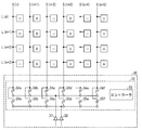
- FIG. 2 is a diagram illustrating a configuration example of a source driver according to Embodiment 1.
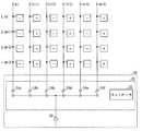
- FIG. 1st write-in period of the source driver which concerns on Embodiment 1 is shown.
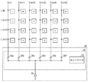
- the state in the 2nd write-in period of the source driver concerning Embodiment 1 is shown.
- the state in the 3rd write period of the source driver which concerns on Embodiment 1 is shown.
- the state in the 4th write-in period of the source driver concerning Embodiment 1 is shown.
- the state in the 5th writing period of the source driver which concerns on Embodiment 1 is shown.
- the state in the 6th write period of the source driver which concerns on Embodiment 1 is shown.
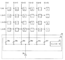
- FIG. 6 is a diagram illustrating a configuration example of a source driver according to Embodiment 2.
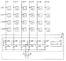
- FIG. The state in the 1st writing period of the source driver which concerns on Embodiment 2 is shown.
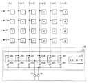
- the state in the 2nd writing period of the source driver which concerns on Embodiment 2 is shown.
- the state in the 3rd write period of the source driver which concerns on Embodiment 2 is shown.
- 6 is a diagram illustrating a configuration example of a display panel 2 according to Embodiment 3.
- FIG. FIG. 3 is a diagram illustrating a configuration of pixels included in the display panel 2. It is a figure which shows the characteristic of various TFT.
- FIG. 1 is a diagram illustrating an overall configuration of a display device 1 according to the first embodiment.
- a display device 1 includes a display panel 2, a gate driver (scanning line driving circuit) 4, a source driver (signal line driving circuit) 30, a common electrode driving circuit 8, a timing controller 10, and a power generation circuit. 13 is provided.
- an active matrix type liquid crystal display device is employed as the display device 1. Therefore, the display panel 2 of the first embodiment is an active matrix type liquid crystal display panel, and the other components described above are for driving the liquid crystal display panel.
- the display panel 2 includes a screen composed of a plurality of pixels arranged in a grid, M gate signal lines (scanning signal lines) G for selecting and scanning the screen in a line-sequential manner, and a selected gate.
- M gate signal lines (scanning signal lines) G for selecting and scanning the screen in a line-sequential manner
- a selected gate for selecting and scanning the screen in a line-sequential manner
- N source signal lines (data signal lines) S for supplying data signals to the pixels of one row included in the signal line are provided.
- the gate signal line G and the source signal line S are orthogonal to each other.
- the gate signal line G connecting the pixels in the m-th row (m is an arbitrary integer) is denoted as G (m).
- G (m) is a gate signal line G connecting pixels in the 10th row
- G (m + 1), G (m + 2), and G (m + 3) are in the 11th, 12th, and 13th rows, respectively.
- a gate signal line G connecting the eye pixels is shown.
- the source signal line S that connects the pixels in the n-th column (n is an arbitrary integer) is denoted as S (n).
- S (n) is a source signal line S connecting pixels in the tenth column
- S (n + 1), S (n + 2), S (n + 3), S (n + 4), and S (n + 5) are respectively
- S (n + 5) is a source signal line S connecting pixels in the 11th, 12th, 13th, 14th, and 15th columns.
- the gate driver 4 scans each gate signal line G line-sequentially from the top to the bottom of the screen.
- the gate driver 4 sequentially outputs to each gate signal line G a voltage for turning on a switching element (TFT) provided in each pixel on the gate signal line G. Accordingly, the gate driver 4 sequentially selects and scans each gate signal line G.
- TFT switching element
- the source driver 30 supplies a source signal from each source signal line S to each pixel on the selected gate signal line G. Specifically, the source driver 30 calculates the value of the voltage to be output to each pixel on the selected gate signal line G based on the input video signal (arrow A), and the voltage of that value Are output from the source output amplifier toward each source signal line S. As a result, a source signal is supplied to each pixel on the selected gate signal line G, and the source signal is written.
- the display device 1 includes a common electrode (not shown) provided for each pixel in the screen.
- the common electrode driving circuit 8 outputs a predetermined common voltage for driving the common electrode to the common electrode based on a signal (arrow B) input from the timing controller 10.
- Timing controller 10 outputs a reference signal for each circuit to operate in synchronization with each circuit. Specifically, the timing controller 10 supplies the gate driver 4 with a gate start pulse signal, a gate clock signal GCK, and a gate output control signal GOE (arrow E). The timing controller 10 outputs a source start pulse signal, a source latch strobe signal, and a source clock signal to the source driver 30 (arrow F).
- the gate driver 4 starts scanning the display panel 2 with the gate start pulse signal received from the timing controller 10 as a cue, and applies to each gate signal line G according to the gate clock signal GCK and the gate output control signal GOE received from the timing controller 10.
- the selection voltage is sequentially applied. Specifically, the gate driver 4 sequentially selects each gate signal line G according to the received gate clock GCK signal.
- the gate driver 4 applies a selection voltage to the selected gate signal line G at the timing when the falling edge of the received gate output control signal GOE is detected. As a result, the gate driver 4 scans the selected gate signal line G.
- the source driver 30 Based on the source start pulse signal received from the timing controller 10, the source driver 30 stores the input image data of each pixel in a register according to the source clock signal, and each source signal of the display panel 2 according to the next source latch strobe signal. Image data is written in line S.
- the power supply generation circuit 13 generates Vdd, Vdd2, Vcc, Vgh, and Vgl, which are voltages necessary for each circuit in the display device 1 to operate. Then, Vcc, Vgh, and Vgl are output to the gate driver 4, Vdd and Vcc are output to the source driver 30, Vcc is output to the timing controller 10, and Vdd 2 is output to the common electrode drive circuit 8.
- the source driver 30 For each of the plurality of gate signal lines G, when attention is paid to a plurality of pixels on the gate signal line G, the source driver 30 generates a source signal for each source signal line S (that is, for each pixel). The source signal is supplied to each source signal line S by inverting the sign (from the reference voltage) of the voltage supplied as.
- the source driver 30 does not invert the polarity (from the reference voltage) of the voltage supplied as the source signal for the plurality of pixels on the source signal line S.
- a source signal is supplied to each source signal line S.
- source signal (+) first data signal
- source signal (+) second data signal
- source signal ( ⁇ ) source signal
- the data signal supplied to the plurality of pixels on the source signal line is the source signal (+), the source signal ( ⁇ ), and the like. It can be switched with.
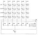
- FIG. 2 is a diagram illustrating a configuration example of the source driver 30 according to the first embodiment.
- the source signal lines S (n) to (n + 5) of the plurality of source signal lines provided in the display panel 2 and the pixel rows L (m) to (n) of the plurality of pixel rows are provided.
- a configuration example of the source driver 30 will be described using (m + 3). Further, illustration and description of other components such as a DA converter generally provided in the source driver 30 are omitted.
- FIG. 2 and subsequent figures show states in a certain frame period, and in FIG. 2 and subsequent pixels, a source signal (+) should be written in pixels indicated by “+” in this frame period. Indicates a pixel. In addition, a pixel indicated by “ ⁇ ” indicates a pixel to which a source signal ( ⁇ ) is to be written in this frame period.
- the frame inversion drive that is, the configuration in which the positive / negative of the source signal to be written to each pixel is inverted every frame period, the first frame period in which the operation described in FIG. The first frame period and the second frame period in which the sign of the source signal to be written in each pixel is inverted alternately exist.
- the source driver 30 includes the number of source output amplifiers 36 that is not the same as the number of source signal lines S as in the conventional display device, but smaller than the number of source signal lines S. ing. Specifically, the source driver 30 of the first embodiment includes one source output amplifier 36.
- the source driver 30 of the first embodiment is configured to supply source signals to the plurality of source signal lines S by this one source output amplifier 36.
- switching means 32 is provided for switching the source signal line S to which the source signal output from the source output amplifier 36 is supplied.
- the switching means 32 includes a plurality of switches 34a to 34f for each source signal line S. One end of each switch 34 is connected to the corresponding source signal line S. The other end of each switch 34 is connected to the output end of the source output amplifier 36. The operation (ie, on / off) of each switch 34 is controlled by the controller 33 provided in the switching unit 32.
- the controller 33 switches the switch to be turned on according to the source signal line S to which the source signal is supplied. As a result, a source signal is supplied to each of the plurality of source signal lines S.
- a first writing period for the source signal lines S (n) to (n + 5).
- the controller 33 switches the corresponding switch 34 to ON and switches the other switches 34 to OFF.
- the corresponding source signal line S is connected to the source output amplifier 36, and the source signal output from the source output amplifier 36 is supplied to the source signal line S. .
- FIG. 3 shows a state in the first write period of the source driver 30 according to the first embodiment.
- the source driver 30 writes a source signal to the source signal line S (n). Therefore, as shown in FIG. 3, the controller 33 turns on the switch 34a corresponding to the source signal line S (n) and turns off the other switches. Thereby, the source output amplifier 36 and the source signal line S (n) are electrically connected, and the source signal output from the source output amplifier 36 is supplied to the source signal line S (n).
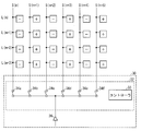
- FIG. 4 shows a state in the second writing period of the source driver 30 according to the first embodiment.
- the source driver 30 writes a source signal to the source signal line S (n + 1). Therefore, as shown in FIG. 4, the controller 33 turns on the switch 34b corresponding to the source signal line S (n + 1) and turns off the other switches. Thereby, the source output amplifier 36 and the source signal line S (n + 1) are electrically connected, and the source signal output from the source output amplifier 36 is supplied to the source signal line S (n + 1).
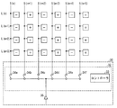
- FIG. 5 shows a state in the third writing period of the source driver 30 according to the first embodiment.
- the source driver 30 writes a source signal to the source signal line S (n + 2). Therefore, as shown in FIG. 5, the controller 33 turns on the switch 34c corresponding to the source signal line S (n + 2) and turns off the other switches.
- the source output amplifier 36 and the source signal line S (n + 2) are electrically connected, and the source signal output from the source output amplifier 36 is supplied to the source signal line S (n + 2).
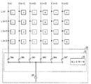
- FIG. 6 shows a state in the fourth writing period of the source driver 30 according to the first embodiment.
- the display device 1 writes a source signal to the source signal line S (n + 3). Therefore, as shown in FIG. 6, the controller 33 of the switching unit 32 turns on the switch 34d corresponding to the source signal line S (n + 3) and turns off the other switches. Thereby, the source output amplifier 36 and the source signal line S (n + 3) are electrically connected, and the source signal output from the source output amplifier 36 is supplied to the source signal line S (n + 3).
- FIG. 7 shows a state in the fifth writing period of the source driver 30 according to the first embodiment.
- the source driver 30 writes a source signal to the source signal line S (n + 4). Therefore, as shown in FIG. 7, the controller 33 of the switching unit 32 turns on the switch 34e corresponding to the source signal line S (n + 4) and turns off the other switches. Thereby, the source output amplifier 36 and the source signal line S (n + 4) are electrically connected, and the source signal output from the source output amplifier 36 is supplied to the source signal line S (n + 4).
- FIG. 8 shows a state in the sixth writing period of the source driver 30 according to the first embodiment.
- the display device 1 writes a source signal to the source signal line S (n + 5). Therefore, as shown in FIG. 8, the controller 33 of the switching unit 32 turns on the switch 34f corresponding to the source signal line S (n + 5) and turns off the other switches. Thereby, the source output amplifier 36 and the source signal line S (n + 5) are electrically connected, and the source signal output from the source output amplifier 36 is supplied to the source signal line S (n + 5).
- the source driver 30 of the first embodiment employs frame inversion driving.
- the source output amplifier 36 changes the source signal potential of the source signal to be supplied every time the target source signal line S is switched in the first to sixth writing periods (that is, every time the writing period is switched). Switch between positive and negative.
- the source output amplifier 36 outputs a source signal ( ⁇ ) having a negative source signal potential in each of the first, third, and fifth writing periods.
- the source signal ( ⁇ ) is supplied to each of the source signal lines S (n), (n + 2), and (n + 4).
- the source output amplifier 36 outputs a source signal (+) having a positive source signal potential.
- the source signal (+) is supplied to each of the source signal lines S (n + 1), (n + 3), and (n + 5).
- each pixel column of the display device 1 has only one of the pixel to which the source signal (+) is written and the pixel to which the source signal ( ⁇ ) is written. Will be.
- the display device 1 has a configuration in which only one source output amplifier is provided and a source signal is supplied from the source output amplifier to each of a plurality of source signal lines.
- the number of source output amplifiers for supplying source signals can be greatly reduced, and the cost associated with the source driver can be reduced. That is, an image can be displayed more efficiently.
- the display device 1 of Embodiment 1 can reduce the total amount of steady current required by the source output amplifier by reducing the number of source output amplifiers. Therefore, the display device 1 according to the first embodiment can reduce power consumption. That is, an image can be displayed more efficiently.
- Embodiment 2 Next, Embodiment 2 of the present invention will be described.
- the first embodiment only one source output amplifier is provided.
- the second embodiment an example in which two source output amplifiers are provided will be described.
- the display device 1 according to the second embodiment is the same as the display device 1 according to the first embodiment except for the points described below.
- FIG. 9 is a diagram illustrating a configuration example of the source driver 30 according to the second embodiment.
- the source signal lines S (n) to (n + 5) of the plurality of source signal lines provided in the display panel 2 and the pixel rows L (m) to A configuration example of the source driver 30 will be described using (m + 3).
- the source driver 30 of the second embodiment includes a number of source output amplifiers that are smaller than the number of source signal lines S. Specifically, the source driver 30 of the second embodiment includes two source output amplifiers 37 and 38.
- the source output amplifier 37 (first source output amplifier) is for supplying a source signal ( ⁇ ) having a negative source signal potential.
- the source output amplifier 38 (second source output amplifier) is for supplying a source signal (+) having a positive source signal potential.
- the source output amplifier 36 of the first embodiment supplies both the source signal (+) and the source signal ( ⁇ ), whereas the source output amplifiers 37 and 38 of the second embodiment have the source signal (+). Supply either +) or source signal (-).
- the source driver 30 of the present embodiment 2 supplies the source signal (+) from the source output amplifier 37 when supplying the source signal ( ⁇ ) to each of the plurality of source signal lines S.
- a source signal is supplied from the source output amplifier 38.
- switching means 32 for switching the source signal line S to which the source signals output from the source output amplifiers 37 and 38 are supplied is provided. Is provided.
- the switching means 32 includes a plurality of switches 34a to 34f for each source signal line S. Further, the switching unit 32 includes a plurality of switches 35a to 35f for each source signal line S.
- each switch 34 One end of each switch 34 is connected to the corresponding source signal line S, and the other end of each switch 34 is connected to the output terminal of the source output amplifier 37. That is, the switches 34a to 34f are for switching the source signal line S to which the source signal output from the source output amplifier 37 is supplied.
- each switch 35 is connected to the corresponding source signal line S, and the other end of each switch 35 is connected to the output terminal of the source output amplifier 38. That is, the switches 35a to 35f are for switching the source signal line S to which the source signal output from the source output amplifier 38 is supplied.
- each switch 34, 35 is controlled by the controller 33 provided in the switching means 32 (ie, on / off).
- the controller 33 turns on the switch 35 corresponding to the source signal line S. At this time, the other switches 34 and 35 are kept OFF. Thereby, the source output amplifier 38 and the source signal line S are electrically connected, and the source signal (+) output from the source output amplifier 38 is supplied to the target source signal line S.
- the controller 33 switches the switch to be turned on according to the source signal line S to which the source signal is output. As a result, a source signal is supplied to each of the plurality of source signal lines S.
- one horizontal period in the display device 1 of Embodiment 2 includes a first writing period, a second writing period, and a third writing period in order.
- the source driver 30 of the second embodiment simultaneously supplies the source signal ( ⁇ ) by the source output amplifier 37 and the source signal (+) by the source output amplifier 38 in each writing period.
- writing to each of the six source signal lines S (source signal lines S (n) to (n + 5)) by three writing periods (first to third writing periods) is realized.
- the controller 33 switches the corresponding switches 34 and 35 to ON, and switches the other switches 34 and 35 to OFF. Accordingly, in each writing period, the corresponding first source signal line S is connected to the source output amplifier 37, and the source signal ( ⁇ ) output from the source output amplifier 37 is connected to the source signal line S. Will be supplied. At the same time, the corresponding second source signal line S is connected to the source output amplifier 38, and the source signal (+) output from the source output amplifier 38 is supplied to the source signal line S.
- FIG. 10 shows a state in the first writing period of the source driver 30 according to the second embodiment.
- the source driver 30 writes a source signal to the source signal lines S (n) and (n + 1).
- the source signal ( ⁇ ) is written to the source signal line S (n) and at the same time the source signal (+) is written to the source signal line S (n + 1). I do.
- the controller 33 turns on the switch 34a corresponding to the source signal line S (n) and turns on the switch 35b corresponding to the source signal line S (n + 1). Set the switch to OFF.
- the source output amplifier 37 and the source signal line S (n) are electrically connected, and the source output amplifier 38 and the source signal line S (n + 1) are electrically connected.
- the source signal ( ⁇ ) output from the source output amplifier 37 is supplied to the source signal line S (n)
- the source signal (+) output from the source output amplifier 38 is supplied to the source signal line S (n + 1). To be supplied.
- FIG. 11 shows a state in the second writing period of the source driver 30 according to the second embodiment.
- the source driver 30 writes a source signal to the source signal lines S (n + 2) and (n + 3).
- the source signal ( ⁇ ) is written to the source signal line S (n + 2), and at the same time, the source signal (+) is written to the source signal line S (n + 3). I do.
- the controller 33 turns on the switch 34c corresponding to the source signal line S (n + 2) and turns on the switch 35d corresponding to the source signal line S (n + 3). Set the switch to OFF.
- the source output amplifier 37 and the source signal line S (n + 2) are electrically connected, and the source output amplifier 38 and the source signal line S (n + 3) are electrically connected.
- the source signal ( ⁇ ) output from the source output amplifier 37 is supplied to the source signal line S (n + 2), and the source signal (+) output from the source output amplifier 38 is the source signal line S (n + 3). To be supplied.
- FIG. 12 shows a state in the third writing period of the source driver 30 according to the second embodiment.
- the source driver 30 writes a source signal to the source signal lines S (n + 4) and (n + 5).
- the source signal ( ⁇ ) is written to the source signal line S (n + 4), and at the same time, the source signal (+) is written to the source signal line S (n + 5). I do.
- the controller 33 turns on the switch 34e corresponding to the source signal line S (n + 4) and turns on the switch 35f corresponding to the source signal line S (n + 5). Set the switch to OFF.
- the source output amplifier 37 and the source signal line S (n + 4) are electrically connected, and the source output amplifier 38 and the source signal line S (n + 5) are electrically connected.
- the source signal ( ⁇ ) output from the source output amplifier 37 is supplied to the source signal line S (n + 4), and the source signal (+) output from the source output amplifier 38 is the source signal line S (n + 5). To be supplied.
- each pixel column of the display device 1 has only one of the pixel to which the source signal (+) is written and the pixel to which the source signal ( ⁇ ) is written. Will be.
- the display device 1 according to the second embodiment has a configuration in which only two source output amplifiers are provided and a source signal is supplied from the source output amplifier to each of a plurality of source signal lines.
- the number of source output amplifiers for supplying source signals can be greatly reduced, and the cost associated with the source driver can be reduced. That is, an image can be displayed more efficiently.
- the display device 1 of Embodiment 2 can reduce the total amount of steady current required by the source output amplifier by reducing the number of source output amplifiers. Therefore, the display device 1 of Embodiment 2 can reduce power consumption. That is, an image can be displayed more efficiently.
- the display device 1 uses the source output amplifiers 37 and 38 that supply one of the source signal (+) and the source signal ( ⁇ ).
- the withstand voltage design range of each source output amplifier is kept on one of the positive side and the negative side. Since it can be narrowed, the power consumption of each source output amplifier can be reduced. Therefore, the display device 1 of the second embodiment can further reduce the power consumption. That is, an image can be displayed more efficiently.
- the display device 1 writes the source signal (+) and the source signal ( ⁇ ) in parallel.
- the source signal writing period can be shortened.
- the source signal writing period can be shortened.
- the display device 1 of Embodiment 2 can display more images within a predetermined unit time, and as a result, display image quality can be improved. That is, an image can be displayed more efficiently.
- FIG. 13 is a diagram illustrating a configuration example of the display panel 2 according to the third embodiment.
- the display device 1 of the first embodiment as illustrated in FIG. 2, one pixel column is connected to one source signal line and driven.
- the display device 1 of Embodiment 3 employs a configuration in which one pixel column is alternately connected to and driven by two source signal lines sandwiching the pixel column. That is, each source signal line adopts a configuration in which two pixel columns sandwiching the source signal line are alternately driven.
- the source driver 30 supplies the source signal to each source signal line S by inverting the polarity of the voltage supplied as the source signal for each source signal line S. However, focusing on the same frame period, only the source signal (+) or the source signal ( ⁇ ) is supplied to each source signal line S. That is, the source driver 30 performs so-called source inversion driving.
- the source driver 30 supplies only the source signal ( ⁇ ) to the source signal lines S (n), (n + 2), and (n + 4).
- only the source signal (+) is supplied to the source signal lines S (n + 1), (n + 3), and (n + 5).
- the source driver 30 performs so-called source inversion driving, but employs a configuration in which one source signal line S alternately drives two pixel columns.
- the pixel to which the source signal (+) is written and the pixel to which the source signal ( ⁇ ) is written are alternately arranged in both the pixel column direction and the pixel row direction. It will be. That is, although the source inversion driving is performed, the same effect as that obtained by performing the dot inversion driving can be obtained.
- the configuration of the switching means 32 shown in each embodiment is only an example.
- the switching means may have any configuration as long as it provides the same action as the switching means 32.
- the source signals are written in parallel to the plurality of source signal lines S by the source output amplifiers 37 and 38, but a configuration in which the source signals are sequentially written may be employed.
- the present invention is not limited to application to a display device that employs source inversion driving.
- so-called source inversion driving is employed in which each pixel column has only a pixel to which a source signal having a positive source signal potential is to be written or a pixel to which a source signal having a negative source signal potential is to be written.
- An example of application to a display device has been described.
- each of the pixel columns there are alternately pixels to which a source signal whose source signal potential is positive and pixels to which a source signal whose source signal potential is negative are written.
- the present invention may be applied to a display device that employs so-called dot inversion driving.
- Modification 4 In the embodiment, an example in which one or two source output amplifiers are provided has been described. However, at least the number of source output amplifiers that is smaller than the number of source signal lines may be provided, and three or more source output amplifiers may be provided. Otherwise.
- FIG. 14 is a diagram illustrating a configuration of pixels included in the display panel 2.
- FIG. 14 illustrates a configuration of two pixels (pixel (n, m) and pixel (n + 1, m)) among a plurality of pixels included in the display panel 2.
- Pixel (n, m) indicates a pixel connected to the source signal line S (n) and the gate signal line G (m).
- Pixel (n + 1, m) indicates a pixel connected to the source signal line S (n + 1) and the gate signal line G (m).
- the other pixels included in the display panel 2 have the same configuration as these pixels.
- the pixel includes a TFT 200 as a switching element.
- the gate electrode of the TFT 200 is connected to the corresponding gate signal line G.
- the source electrode of the TFT 200 is connected to the corresponding source signal line S.
- the drain electrode of the TFT 200 is connected to the liquid crystal capacitor Clc and the storage capacitor Ccs.
- the source signal is supplied from the drain electrode of the TFT 200 to the pixel electrode of the liquid crystal capacitor Clc and the storage capacitor Ccs.
- the arrangement direction of the liquid crystal sealed between the pixel electrode of the liquid crystal capacitor Clc and the common electrode is supplied to the pixel. It changes according to the difference between the voltage level of the source signal and the voltage level supplied to the common electrode, and an image corresponding to this difference is displayed.
- the pixel can maintain a state where an image is displayed for a certain period of time due to the electric charge stored in the storage capacitor Ccs.
- a TFT using a so-called oxide semiconductor is employed as the TFT 200, and in particular, indium (In), gallium (Ga), and zinc (Zn) are used as the oxide semiconductor.
- FIG. 15 shows the characteristics of various TFTs.
- FIG. 15 shows the characteristics of a TFT using an oxide semiconductor, a TFT using a-Si (amorphous silicon), and a TFT using LTPS (Low Temperature Poly Silicon).
- the horizontal axis (Vgh) indicates the voltage value of the ON voltage supplied to the gate in each TFT
- the vertical axis (Id) indicates the amount of current between the source and drain in each TFT.
- a period indicated as “TFT-on” in the figure indicates a period in which the transistor is on according to the voltage value of the on-voltage, and a period indicated as “TFT-off” in the figure. Indicates a period of OFF state according to the voltage value of the ON voltage.
- a TFT using an oxide semiconductor has higher electron mobility in the on state than a TFT using a-Si.
- a TFT using a-Si has an Id current of 1 uA at the time of TFT-on, whereas a TFT using an oxide semiconductor has its TFT-on.
- Id current at the time is about 20 to 50 uA.
- a TFT using an oxide semiconductor has an electron mobility about 20 to 50 times higher in an on state than a TFT using a-Si, and has an excellent on-characteristic. .
- the display device 1 of the present embodiment employs a TFT using such an oxide semiconductor for each pixel.
- the display device 1 of the present embodiment has excellent TFT on-characteristics, pixels can be driven by smaller TFTs, so that the area ratio occupied by TFTs in each pixel is reduced. can do. That is, the aperture ratio in each pixel can be increased, and the backlight transmittance can be increased. As a result, a backlight with low power consumption can be adopted or the luminance of the backlight can be suppressed, so that power consumption can be reduced.
- the writing time of the source signal to each pixel can be shortened, so that the refresh rate of the display panel 2 can be easily increased.
- the TFT using an oxide semiconductor has less leakage current in the off state than the TFT using a-Si.
- a TFT using a-Si has an Id current of 10 pA at the time of TFT-off, whereas a TFT using an oxide semiconductor is at the time of TFT-off.
- the Id current is about 0.1 pA.
- the TFT using an oxide semiconductor has a leakage current in an off state of about 1/100 of that of a TFT using a-Si, and no leakage current is generated. It turns out that it is excellent.
- the display device 1 of this embodiment has excellent TFT off characteristics, the state in which the source signals of each of the plurality of pixels of the display panel are written can be maintained for a long period of time.
- the refresh rate of the display panel 2 can be easily lowered.
- the display device includes a display panel having a plurality of gate signal lines and a plurality of source signal lines, a gate driver that sequentially selects and scans the plurality of gate signal lines, and the selected display device.
- a source driver for supplying a data signal from the plurality of source signal lines to each of the plurality of pixels on the gate signal line, wherein the source driver is smaller in number than the number of the plurality of source signal lines.
- the first data signal and the second data signal are alternately supplied, and for each of the plurality of source signal lines, the first data signal is supplied to a plurality of pixels on the source signal line.
- only one of the second data signals is supplied, and each time the frame period is switched, a data signal supplied to a plurality of pixels on the source signal line for each of the plurality of source signal lines. Are switched between the first data signal and the second data signal.
- the source driver includes one source output amplifier, and the switching unit changes the supply destination of the data signal each time the one source output amplifier outputs a data signal.
- the source signal line is switched to the source signal line to which the data signal is to be supplied.
- the cost associated with the source driver can be further reduced.
- the total amount of steady current required by the source output amplifier can be further reduced. Therefore, power consumption can be further reduced. That is, an image can be displayed more efficiently.
- the one source output amplifier alternately outputs a first data signal having a positive data signal potential and a second data signal having a negative data signal potential.
- the first data signal of the plurality of source signal lines is supplied as the supply destination of the first data signal.
- the supply destination of the second data signal is changed to the second source signal line of the plurality of source signal lines. It is preferable to switch to the source signal line to which the data signal is to be supplied.
- the source driver outputs a first source output amplifier that outputs a first data signal having a positive data signal potential and a second data signal that outputs a second data signal having a negative data signal potential.
- the switching means changes the supply destination of the first data signal to the plurality of sources.
- the second source output amplifier outputs the second data signal
- the supply of the second data signal is switched to the source signal line to which the first data signal of the signal line is to be supplied.
- the destination is switched to the source signal line to which the second data signal is to be supplied among the plurality of source signal lines.
- the cost associated with the source driver can be further reduced.
- the total amount of steady current required by the source output amplifier can be further reduced. Therefore, power consumption can be further reduced. That is, an image can be displayed more efficiently.
- the withstand voltage design range of each source output amplifier compared to a configuration using a source output amplifier that supplies both a first data signal having a positive data signal potential and a second data signal having a negative data signal potential. Can be narrowed by fitting it on one of the positive side and the negative side, so that the power consumption of each source output amplifier can be reduced. Therefore, power consumption can be further reduced. That is, an image can be displayed more efficiently.
- the output of the first data signal by the first source output amplifier and the output of the second data signal by the second source output amplifier are performed in parallel. It is preferable that the supply of the first data signal to the source signal line and the supply of the second data signal to the source signal line are performed in parallel.
- the source signal writing period can be shortened. That is, since the horizontal scanning period can be shortened, more images can be displayed within a predetermined unit time, and as a result, the display image quality can be improved. That is, an image can be displayed more efficiently.
- an oxide semiconductor is preferably used for a semiconductor layer of each TFT (switching element) of each of the plurality of pixels included in the display panel.
- the oxide semiconductor is preferably IGZO (InGaZnOx).
- a TFT using an oxide semiconductor (in particular, IGZO having better on characteristics and off characteristics) having excellent on characteristics and off characteristics is adopted for each pixel.
- the display panel can be driven with less power consumption. That is, an image can be displayed more efficiently.
- the display device according to the present invention can be used in various display devices employing an active matrix method, such as a liquid crystal display device, an organic EL display device, and electronic paper.
Landscapes
- Engineering & Computer Science (AREA)
- Chemical & Material Sciences (AREA)
- Crystallography & Structural Chemistry (AREA)
- Physics & Mathematics (AREA)
- Computer Hardware Design (AREA)
- General Physics & Mathematics (AREA)
- Theoretical Computer Science (AREA)
- Control Of Indicators Other Than Cathode Ray Tubes (AREA)
- Liquid Crystal Display Device Control (AREA)
Abstract
本発明の目的は、構成が簡素で、消費電力が小さい表示装置を提供することである。本発明の表示装置は、複数のソース信号ライン(S)の数よりも少ない数のソース出力アンプ(36)と、ソース出力アンプ(36)から出力されたデータ信号を複数のソース信号ライン(S)のいずれか1つに供給する切り替え手段(32)とを有し、ソース出力アンプ(36)は、隣り合うソース信号ライン(S)には極性の異なるデータ信号を出力し、それぞれのソース信号ライン(S)に供給するデータ信号の極性をフレーム期間ごとに切り替えて出力する。
Description
本発明は、表示装置に関する。
近年、液晶表示装置に代表される薄型、軽量、および低消費電力の表示装置が盛んに活用されている。こうした表示装置は、例えば携帯電話、スマートフォン、PDA(携帯型情報端末)、電子ブック、ラップトップ型パーソナルコンピュータ等への搭載が顕著である。また、今後はより薄型の表示装置である電子ペーパーの開発および普及も急速に進むことが期待されている。
このような表示装置の多くには、アクティブマトリクス方式が採用されている。一般的に、アクティブマトリクス型の表示装置の画面は、格子状に配置された複数の画素を備えて構成されている。これに対応して、表示装置は、複数の画素行を順次選択するための複数のゲート信号ラインと、選択された画素行の各々の画素に対してソース信号を供給するための複数のソース信号ラインとを備えている。そして、ソースドライバが備えるアナログアンプ(以下、「ソース出力アンプ」と示す。)から、複数のソース信号ラインの各々に対して、画像データとしてのデータ信号(以下、「ソース信号」と示す。)を供給することにより、選択された画素行の各々の画素に対して、ソース信号を書き込む構成を採用している。
このために、例えば、下記特許文献1(図6)に開示されているように、従来の表示装置においては、ソース信号ライン毎の複数のソース出力アンプがソースドライバに設けられている。そして、複数のソース信号ラインの各々に対してソース信号を供給する際には、ソース信号の供給対象のソース信号ラインが切り替わるごとに、使用するソース出力アンプを、このソース信号ラインと対に設けられているソース出力アンプに切り替える構成を採用している。例えば、表示装置の解像度が1366×768の場合、ソースドライバは、1366個のソース出力アンプを備えることとなる。
近年、表示装置の高精細化および高解像度化が進んでおり、これに伴い、表示装置においては、構成の簡素化や、消費電力の削減等、より効率的に画像を表示するよう要求されてきている。しかしながら、上記特許文献1に開示されている技術では、膨大な数のソース出力アンプを備えているため、構成が複雑化し、消費電力が増加する等、より効率的に画像を表示することができない。
本発明は、前記の問題に鑑みてなされたものであり、その目的は、より効率的に画像を表示することができる表示装置を提供することにある。
本発明に係る表示装置は、上述した課題を解決するため、複数のゲート信号ラインおよび複数のソース信号ラインを有する表示パネルと、前記複数のゲート信号ラインを順次選択して走査するゲートドライバと、選択されたゲート信号ライン上の複数の画素の各々に対し、前記複数のソース信号ラインからデータ信号を供給するソースドライバと、を備え、前記ソースドライバは、前記複数のソース信号ラインの数よりも少ない数のソース出力アンプと、前記ソース出力アンプがデータ信号を出力する毎に、当該データ信号の供給先を、前記複数のソース信号ラインのうちの当該データ信号が供給されるべきソース信号ラインへ切り替える切り替え手段とを有し、前記ソース出力アンプから出力された、データ信号電位が正となる第1のデータ信号、およびデータ信号電位が負となる第2のデータ信号の供給先を、前記切り替え手段によって切り替えることにより、前記複数のゲート信号ラインの各々について、当該ゲート信号ライン上の複数の画素に対しては、前記第1のデータ信号および前記第2のデータ信号を交互に供給するとともに、前記複数のソース信号ラインの各々について、当該ソース信号ライン上の複数の画素に対しては、前記第1のデータ信号または前記第2のデータ信号のいずれか一方のみを供給し、フレーム期間が切り替わるごとに、前記複数のソース信号ラインの各々について、当該ソース信号ライン上の複数の画素に対して供給されるデータ信号を、前記第1のデータ信号と前記第2のデータ信号とで切り替えることを特徴とする。
この構成によれば、従来の表示装置のように、ソース信号ライン毎にソース出力アンプを設ける構成を採用するよりも、ソース出力アンプの数を減らすことができるので、ソースドライバに係るコストを削減することができる。また、ソース出力アンプの数を減らすことにより、ソース出力アンプが必要とする定常電流の総量を削減することができる。したがって、消費電力を削減することができる。すなわち、より効率的に画像を表示することができる。
本発明に係る表示装置によれば、より効率的に画像を表示することができるという効果を奏する。
本発明に係る実施形態について、図面を参照して以下に説明する。
(実施形態1)
まず、本発明の実施形態1について説明する。実施形態1に係る表示装置1の構成について、図1を参照して説明する。図1は、実施形態1に係る表示装置1の全体構成を示す図である。この図に示すように、表示装置1は、表示パネル2、ゲートドライバ(走査線駆動回路)4、ソースドライバ(信号線駆動回路)30、共通電極駆動回路8、タイミングコントローラ10、および電源生成回路13を備えている。
まず、本発明の実施形態1について説明する。実施形態1に係る表示装置1の構成について、図1を参照して説明する。図1は、実施形態1に係る表示装置1の全体構成を示す図である。この図に示すように、表示装置1は、表示パネル2、ゲートドライバ(走査線駆動回路)4、ソースドライバ(信号線駆動回路)30、共通電極駆動回路8、タイミングコントローラ10、および電源生成回路13を備えている。
本実施形態1では、表示装置1としてアクティブマトリクス型の液晶表示装置を採用している。したがって、本実施形態1の表示パネル2は、アクティブマトリクス型の液晶表示パネルであり、上記したその他の構成要素は、液晶表示パネルを駆動するためのものである。
表示パネル2は、格子状に配置された複数の画素からなる画面と、前記画面を線順次に選択して走査するためのM本のゲート信号ライン(走査信号線)Gと、選択されたゲート信号ラインに含まれる一行分の画素のそれぞれにデータ信号を供給するためのN本のソース信号ライン(データ信号線)Sとを備えている。ゲート信号ラインGとソース信号ラインSとは互いに直交している。
以降の説明では、m行目(mは任意の整数)の画素を接続するゲート信号ラインGを、G(m)と示す。例えば、G(m)を10行目の画素を接続するゲート信号ラインGとした場合、G(m+1),G(m+2),G(m+3)は、それぞれ11行目,12行目,13行目の画素を接続するゲート信号ラインGを示す。
また、以降の説明では、n列目(nは任意の整数)の画素を接続するソース信号ラインSを、S(n)と示す。例えば、S(n)を10列目の画素を接続するソース信号ラインSとした場合、S(n+1),S(n+2),S(n+3),S(n+4),S(n+5)は、それぞれ11列目,12列目,13列目,14列目,15列目の画素を接続するソース信号ラインSを示す。
ゲートドライバ4は、各ゲート信号ラインGを画面の上から下に向かって線順次走査する。ゲートドライバ4は、各ゲート信号ラインGに対して、ゲート信号ラインG上の各画素に備えられたスイッチング素子(TFT)をオン状態にさせるための電圧を順次出力する。これにより、ゲートドライバ4は、各ゲート信号ラインGを順次選択して走査する。
ソースドライバ30は、選択されたゲート信号ラインG上の各画素に対して、各ソース信号ラインSからソース信号を供給する。具体的に説明すると、ソースドライバ30は、入力された映像信号(矢印A)に基づいて、選択されたゲート信号ラインG上の各画素に出力すべき電圧の値を算出し、その値の電圧をソース出力アンプから各ソース信号ラインSに向けて出力する。その結果、選択されたゲート信号ラインG上にある各画素に対してソース信号が供給され、ソース信号が書き込まれることとなる。
表示装置1は、画面内の各画素に対して設けられる共通電極(不図示)を備えている。共通電極駆動回路8は、タイミングコントローラ10から入力される信号(矢印B)に基づき、共通電極を駆動するための所定の共通電圧を共通電極に出力する。
タイミングコントローラ10は、各回路が同期して動作するための基準となる信号を各回路に対して出力する。具体的には、タイミングコントローラ10は、ゲートドライバ4に対して、ゲートスタートパルス信号、ゲートクロック信号GCK、およびゲート出力制御信号GOEを供給する(矢印E)。また、タイミングコントローラ10は、ソースドライバ30に対しては、ソーススタートパルス信号、ソースラッチストローブ信号、およびソースクロック信号を出力する(矢印F)。
ゲートドライバ4は、タイミングコントローラ10から受け取ったゲートスタートパルス信号を合図に表示パネル2の走査を開始し、タイミングコントローラ10から受け取ったゲートクロック信号GCKおよびゲート出力制御信号GOEに従って各ゲート信号ラインGに対して、順次選択電圧を印加していく。この点について具体的に説明すると、ゲートドライバ4は、受け取ったゲートクロックGCK信号に従って、各ゲート信号ラインGを順次選択する。そして、ゲートドライバ4は、受け取ったゲート出力制御信号GOEの立ち下りを検出したタイミングで、選択したゲート信号ラインGに対して、選択電圧を印加する。これにより、ゲートドライバ4は、選択したゲート信号ラインGを走査することとなる。
ソースドライバ30は、タイミングコントローラ10から受け取ったソーススタートパルス信号を基に、入力された各画素の画像データをソースクロック信号に従ってレジスタに蓄え、次のソースラッチストローブ信号に従って表示パネル2の各ソース信号ラインSに画像データを書き込む。
電源生成回路13は、表示装置1内の各回路が動作するために必要な電圧であるVdd、Vdd2、Vcc、Vgh、およびVglを生成する。そして、Vcc、Vgh、Vglをゲートドライバ4に出力し、VddおよびVccをソースドライバ30に出力し、Vccをタイミングコントローラ10に出力し、Vdd2を共通電極駆動回路8に出力する。
(書き込み動作)
ここで、複数のゲート信号ラインGの各々について、当該ゲート信号ラインG上の複数の画素に着目すると、ソースドライバ30は、1つのソース信号ラインS毎(すなわち、1画素毎)に、ソース信号として供給する電圧の(基準電圧からの)正負を反転させて、各ソース信号ラインSに対してソース信号を供給する。
ここで、複数のゲート信号ラインGの各々について、当該ゲート信号ラインG上の複数の画素に着目すると、ソースドライバ30は、1つのソース信号ラインS毎(すなわち、1画素毎)に、ソース信号として供給する電圧の(基準電圧からの)正負を反転させて、各ソース信号ラインSに対してソース信号を供給する。
一方、複数のソース信号ラインSの各々について、当該ソース信号ラインS上の複数の画素に対しては、ソースドライバ30は、ソース信号として供給する電圧の(基準電圧からの)正負を反転させずに、各ソース信号ラインSに対してソース信号を供給する。
これにより、表示パネル2上においては、同一のフレーム期間において、ソース信号電位が正となるソース信号(第1のデータ信号。以下、「ソース信号(+)」と示す。)のみが供給されるソース信号ラインSと、ソース信号電位が負となるソース信号(第2のデータ信号。以下、「ソース信号(-)」と示す。)のみが供給されるソース信号ラインSとが、交互に存在することとなる。
そして、図2~12に示すように、各画素行には、ソース信号(+)が書き込まれる画素と、ソース信号(-)が書き込まれる画素とが交互に存在することとなり、各画素列には、ソース信号(+)が書き込まれる画素、またはソース信号(-)が書き込まれる画素のいずれか一方のみが存在することとなる。
なお、フレーム期間が切り替わるごとに、複数のソース信号ラインSの各々について、当該ソース信号ライン上の複数の画素に対して供給されるデータ信号は、ソース信号(+)とソース信号(-)とで切り替えられる。
以上のようなディスプレイ駆動方式を、「フレーム反転駆動」と称する。
(ソースドライバ30の構成例)
ここで、ソースドライバ30の構成例について説明する。図2は、実施形態1に係るソースドライバ30の構成例を示す図である。ここでは、説明を分かり易くするため、表示パネル2が備える複数のソース信号ラインのうちのソース信号ラインS(n)~(n+5)、および複数の画素行のうちの画素行L(m)~(m+3)を用いて、ソースドライバ30の構成例を説明する。また、ソースドライバ30が一般的に備えるDAコンバータ等の他の構成部品について図示および説明を省略する。
ここで、ソースドライバ30の構成例について説明する。図2は、実施形態1に係るソースドライバ30の構成例を示す図である。ここでは、説明を分かり易くするため、表示パネル2が備える複数のソース信号ラインのうちのソース信号ラインS(n)~(n+5)、および複数の画素行のうちの画素行L(m)~(m+3)を用いて、ソースドライバ30の構成例を説明する。また、ソースドライバ30が一般的に備えるDAコンバータ等の他の構成部品について図示および説明を省略する。
なお、図2以降は、あるフレーム期間における状態を示したものであり、この図2以降において、「+」が示されている画素は、このフレーム期間において、ソース信号(+)が書き込まれるべき画素を示す。また、「-」が示されている画素は、このフレーム期間において、ソース信号(-)が書き込まれるべき画素を示す。
本実施形態では、フレーム反転駆動、すなわち、フレーム期間毎に各画素に書き込まれるべきソース信号の正負が反転する構成を採用しているので、図2以降で説明する動作を行う第1のフレーム期間と、この第1のフレーム期間とは各画素に書き込まれるべきソース信号の正負が反転する第2のフレーム期間とが交互に存在することなる。
図2に示すように、本実施形態1のソースドライバ30は、従来の表示装置のようにソース信号ラインSと同数ではなく、ソース信号ラインSの数よりも少ない数のソース出力アンプ36を備えている。具体的には、本実施形態1のソースドライバ30は、1つのソース出力アンプ36を備えている。
すなわち、本実施形態1のソースドライバ30は、この1つのソース出力アンプ36によって、複数のソース信号ラインSに対して、ソース信号を供給する構成となっている。
これを実現するために、ソース出力アンプ36の出力側には、ソース出力アンプ36から出力されたソース信号の供給先のソース信号ラインSを切り替えるための、切り替え手段32が設けられている。
図2に示す例では、切り替え手段32は、ソース信号ラインS毎の、複数のスイッチ34a~fを備えている。各スイッチ34の一端は、対応するソース信号ラインSに接続されている。各スイッチ34の他端は、ソース出力アンプ36の出力端に接続されている。各スイッチ34は、切り替え手段32が備えるコントローラ33によって、その動作(すなわちオン/オフ)が制御される。
(ソースドライバ30による書き込み動作)
あるソース信号ラインSに対するソース信号の供給が行われる際、コントローラ33は、このソース信号ラインSに対応するスイッチ34をONにする。この時、その他のスイッチ34についてはOFFのままとする。これにより、ソース出力アンプ36とこのソース信号ラインSとが電気的に接続され、ソース出力アンプ36から出力されたソース信号が、対象のソース信号ラインSへ供給されるようになる。
あるソース信号ラインSに対するソース信号の供給が行われる際、コントローラ33は、このソース信号ラインSに対応するスイッチ34をONにする。この時、その他のスイッチ34についてはOFFのままとする。これにより、ソース出力アンプ36とこのソース信号ラインSとが電気的に接続され、ソース出力アンプ36から出力されたソース信号が、対象のソース信号ラインSへ供給されるようになる。
コントローラ33は、ソース出力アンプ36からソース信号が出力される毎に、ONにする対象のスイッチを、ソース信号の供給先のソース信号ラインSに応じて切り替える。これにより、複数のソース信号ラインSの各々に対して、ソース信号が供給されることとなる。
例えば、本実施形態1の表示装置1における1水平期間には、順に、第1の書き込み期間、第2の書き込み期間、第3の書き込み期間、第4の書き込み期間、第5の書き込み期間、および第6の書き込み期間が含まれている。この第1~6の書き込み期間は、ソース信号ラインS(n)~(n+5)の各々に対する書き込み期間である。
コントローラ33は、上記書き込み期間が切り替わる毎に、対応するスイッチ34をONに切り替え、それ以外のスイッチ34をOFFに切り替える。これにより、各書き込み期間においては、対応するソース信号ラインSがソース出力アンプ36と接続され、このソース信号ラインSに対して、ソース出力アンプ36から出力されたソース信号が供給されることとなる。
以下、図3~8を参照して、本実施形態1のソースドライバ30によるソース信号の書き込み動作の具体例を説明する。
(第1の書き込み期間)
図3は、実施形態1に係るソースドライバ30の第1の書き込み期間における状態を示す。第1の書き込み期間においては、ソースドライバ30は、ソース信号ラインS(n)に対してソース信号の書き込みを行なう。このため、コントローラ33は、図3に示すように、このソース信号ラインS(n)に対応するスイッチ34aをONにし、それ以外のスイッチについてはOFFにする。これにより、ソース出力アンプ36とソース信号ラインS(n)とが電気的に接続され、ソース出力アンプ36から出力されたソース信号が、ソース信号ラインS(n)に供給される。
図3は、実施形態1に係るソースドライバ30の第1の書き込み期間における状態を示す。第1の書き込み期間においては、ソースドライバ30は、ソース信号ラインS(n)に対してソース信号の書き込みを行なう。このため、コントローラ33は、図3に示すように、このソース信号ラインS(n)に対応するスイッチ34aをONにし、それ以外のスイッチについてはOFFにする。これにより、ソース出力アンプ36とソース信号ラインS(n)とが電気的に接続され、ソース出力アンプ36から出力されたソース信号が、ソース信号ラインS(n)に供給される。
(第2の書き込み期間)
図4は、実施形態1に係るソースドライバ30の第2の書き込み期間における状態を示す。第2の書き込み期間においては、ソースドライバ30は、ソース信号ラインS(n+1)に対してソース信号の書き込みを行なう。このため、コントローラ33は、図4に示すように、このソース信号ラインS(n+1)に対応するスイッチ34bをONにし、それ以外のスイッチについてはOFFにする。これにより、ソース出力アンプ36とソース信号ラインS(n+1)とが電気的に接続され、ソース出力アンプ36から出力されたソース信号が、ソース信号ラインS(n+1)に供給される。
図4は、実施形態1に係るソースドライバ30の第2の書き込み期間における状態を示す。第2の書き込み期間においては、ソースドライバ30は、ソース信号ラインS(n+1)に対してソース信号の書き込みを行なう。このため、コントローラ33は、図4に示すように、このソース信号ラインS(n+1)に対応するスイッチ34bをONにし、それ以外のスイッチについてはOFFにする。これにより、ソース出力アンプ36とソース信号ラインS(n+1)とが電気的に接続され、ソース出力アンプ36から出力されたソース信号が、ソース信号ラインS(n+1)に供給される。
(第3の書き込み期間)
図5は、実施形態1に係るソースドライバ30の第3の書き込み期間における状態を示す。第3の書き込み期間においては、ソースドライバ30は、ソース信号ラインS(n+2)に対してソース信号の書き込みを行なう。このため、コントローラ33は、図5に示すように、このソース信号ラインS(n+2)に対応するスイッチ34cをONにし、それ以外のスイッチについてはOFFにする。これにより、ソース出力アンプ36とソース信号ラインS(n+2)とが電気的に接続され、ソース出力アンプ36から出力されたソース信号が、ソース信号ラインS(n+2)に供給される。
図5は、実施形態1に係るソースドライバ30の第3の書き込み期間における状態を示す。第3の書き込み期間においては、ソースドライバ30は、ソース信号ラインS(n+2)に対してソース信号の書き込みを行なう。このため、コントローラ33は、図5に示すように、このソース信号ラインS(n+2)に対応するスイッチ34cをONにし、それ以外のスイッチについてはOFFにする。これにより、ソース出力アンプ36とソース信号ラインS(n+2)とが電気的に接続され、ソース出力アンプ36から出力されたソース信号が、ソース信号ラインS(n+2)に供給される。
(第4の書き込み期間)
図6は、実施形態1に係るソースドライバ30の第4の書き込み期間における状態を示す。第4の書き込み期間においては、表示装置1は、ソース信号ラインS(n+3)に対してソース信号の書き込みを行なう。このため、切り替え手段32のコントローラ33は、図6に示すように、このソース信号ラインS(n+3)に対応するスイッチ34dをONにし、それ以外のスイッチについてはOFFにする。これにより、ソース出力アンプ36とソース信号ラインS(n+3)とが電気的に接続され、ソース出力アンプ36から出力されたソース信号が、ソース信号ラインS(n+3)に供給される。
図6は、実施形態1に係るソースドライバ30の第4の書き込み期間における状態を示す。第4の書き込み期間においては、表示装置1は、ソース信号ラインS(n+3)に対してソース信号の書き込みを行なう。このため、切り替え手段32のコントローラ33は、図6に示すように、このソース信号ラインS(n+3)に対応するスイッチ34dをONにし、それ以外のスイッチについてはOFFにする。これにより、ソース出力アンプ36とソース信号ラインS(n+3)とが電気的に接続され、ソース出力アンプ36から出力されたソース信号が、ソース信号ラインS(n+3)に供給される。
(第5の書き込み期間)
図7は、実施形態1に係るソースドライバ30の第5の書き込み期間における状態を示す。第5の書き込み期間においては、ソースドライバ30は、ソース信号ラインS(n+4)に対してソース信号の書き込みを行なう。このため、切り替え手段32のコントローラ33は、図7に示すように、このソース信号ラインS(n+4)に対応するスイッチ34eをONにし、それ以外のスイッチについてはOFFにする。これにより、ソース出力アンプ36とソース信号ラインS(n+4)とが電気的に接続され、ソース出力アンプ36から出力されたソース信号が、ソース信号ラインS(n+4)に供給される。
図7は、実施形態1に係るソースドライバ30の第5の書き込み期間における状態を示す。第5の書き込み期間においては、ソースドライバ30は、ソース信号ラインS(n+4)に対してソース信号の書き込みを行なう。このため、切り替え手段32のコントローラ33は、図7に示すように、このソース信号ラインS(n+4)に対応するスイッチ34eをONにし、それ以外のスイッチについてはOFFにする。これにより、ソース出力アンプ36とソース信号ラインS(n+4)とが電気的に接続され、ソース出力アンプ36から出力されたソース信号が、ソース信号ラインS(n+4)に供給される。
(第6の書き込み期間)
図8は、実施形態1に係るソースドライバ30の第6の書き込み期間における状態を示す。第6の書き込み期間においては、表示装置1は、ソース信号ラインS(n+5)に対してソース信号の書き込みを行なう。このため、切り替え手段32のコントローラ33は、図8に示すように、このソース信号ラインS(n+5)に対応するスイッチ34fをONにし、それ以外のスイッチについてはOFFにする。これにより、ソース出力アンプ36とソース信号ラインS(n+5)とが電気的に接続され、ソース出力アンプ36から出力されたソース信号が、ソース信号ラインS(n+5)に供給される。
図8は、実施形態1に係るソースドライバ30の第6の書き込み期間における状態を示す。第6の書き込み期間においては、表示装置1は、ソース信号ラインS(n+5)に対してソース信号の書き込みを行なう。このため、切り替え手段32のコントローラ33は、図8に示すように、このソース信号ラインS(n+5)に対応するスイッチ34fをONにし、それ以外のスイッチについてはOFFにする。これにより、ソース出力アンプ36とソース信号ラインS(n+5)とが電気的に接続され、ソース出力アンプ36から出力されたソース信号が、ソース信号ラインS(n+5)に供給される。
(ソース信号の正負の切り替え)
なお、既に説明したとおり、本実施形態1のソースドライバ30はフレーム反転駆動を採用している。これに応じて、ソース出力アンプ36は、上記第1~6の書き込み期間において、対象のソース信号ラインSが切り替わる毎(すなわち、書き込み期間が切り替わる毎)に、供給するソース信号のソース信号電位の正負を切り替える。
なお、既に説明したとおり、本実施形態1のソースドライバ30はフレーム反転駆動を採用している。これに応じて、ソース出力アンプ36は、上記第1~6の書き込み期間において、対象のソース信号ラインSが切り替わる毎(すなわち、書き込み期間が切り替わる毎)に、供給するソース信号のソース信号電位の正負を切り替える。
例えば、図2~8に示した各画素行に対し、ソース出力アンプ36は、第1,3,5の書き込み期間の各々において、ソース信号電位が負となるソース信号(-)を出力する。これにより、ソース信号ラインS(n),(n+2),(n+4)の各々に対して、ソース信号(-)が供給されることとなる。
一方、第2,4,6の書き込み期間の各々においては、ソース出力アンプ36は、ソース信号電位が正となるソース信号(+)を出力する。これにより、ソース信号ラインS(n+1),(n+3),(n+5)の各々に対して、ソース信号(+)が供給されることとなる。
これにより、表示装置1の各画素行の各々は、図2~8に示すように、ソース信号(+)が書き込まれた画素と、ソース信号(-)が書き込まれた画素とが、交互に存在することとなる。一方、表示装置1の各画素列の各々は、図2~8に示すように、ソース信号(+)が書き込まれた画素またはソース信号(-)が書き込まれた画素のいずれか一方のみが存在することとなる。
(効果)
このように、本実施形態1の表示装置1は、ソース出力アンプを1つだけ設け、このソース出力アンプから複数のソース信号ラインの各々に対してソース信号を供給する構成とした。これにより、ソース信号を供給するためのソース出力アンプの数を大幅に減らすことができるので、ソースドライバに係るコストを削減することができる。すなわち、より効率的に画像を表示することができる。
このように、本実施形態1の表示装置1は、ソース出力アンプを1つだけ設け、このソース出力アンプから複数のソース信号ラインの各々に対してソース信号を供給する構成とした。これにより、ソース信号を供給するためのソース出力アンプの数を大幅に減らすことができるので、ソースドライバに係るコストを削減することができる。すなわち、より効率的に画像を表示することができる。
また、本実施形態1の表示装置1は、ソース出力アンプの数を減らすことにより、ソース出力アンプが必要とする定常電流の総量を削減することができる。したがって、本実施形態1の表示装置1は、消費電力を削減することができる。すなわち、より効率的に画像を表示することができる。
(実施形態2)
次に、本発明の実施形態2について説明する。実施形態1では、ソース出力アンプを1つだけ設ける構成とした。この実施形態2では、2つのソース出力アンプを設ける例を説明する。なお、実施形態2の表示装置1において、以下に説明する以外の点は、実施形態1の表示装置1と同様であるため、説明を省略する。
次に、本発明の実施形態2について説明する。実施形態1では、ソース出力アンプを1つだけ設ける構成とした。この実施形態2では、2つのソース出力アンプを設ける例を説明する。なお、実施形態2の表示装置1において、以下に説明する以外の点は、実施形態1の表示装置1と同様であるため、説明を省略する。
(ソースドライバ30の構成例)
まず、ソースドライバ30の構成例について説明する。図9は、実施形態2に係るソースドライバ30の構成例を示す図である。ここでも、実施形態1と同様に、表示パネル2が備える複数のソース信号ラインのうちのソース信号ラインS(n)~(n+5)、および複数の画素行のうちの画素行L(m)~(m+3)を用いて、ソースドライバ30の構成例を説明する。
まず、ソースドライバ30の構成例について説明する。図9は、実施形態2に係るソースドライバ30の構成例を示す図である。ここでも、実施形態1と同様に、表示パネル2が備える複数のソース信号ラインのうちのソース信号ラインS(n)~(n+5)、および複数の画素行のうちの画素行L(m)~(m+3)を用いて、ソースドライバ30の構成例を説明する。
図9に示すように、本実施形態2のソースドライバ30は、ソース信号ラインSの数よりも少ない数のソース出力アンプを備えている。具体的には、本実施形態2のソースドライバ30は、2つのソース出力アンプ37,38を備えている。
ソース出力アンプ37(第1のソース出力アンプ)は、ソース信号電位が負となるソース信号(-)を供給するためのものである。一方、ソース出力アンプ38(第2のソース出力アンプ)は、ソース信号電位が正となるソース信号(+)を供給するためのものである。
すなわち、実施形態1のソース出力アンプ36が、ソース信号(+)およびソース信号(-)の双方を供給するものであったの対し、実施形態2のソース出力アンプ37,38は、ソース信号(+)またはソース信号(-)の一方を供給する。
本実施形態2のソースドライバ30は、複数のソース信号ラインSの各々に対して、ソース信号(-)を供給する場合にはソース出力アンプ37から、ソース信号(+)を供給する場合にはソース出力アンプ38から、ソース信号を供給する構成となっている。
これを実現するために、ソース出力アンプ37,38の各々の出力側には、ソース出力アンプ37,38から出力されたソース信号の供給先のソース信号ラインSを切り替えるための、切り替え手段32が設けられている。
例えば、図9に示す例では、切り替え手段32は、ソース信号ラインS毎の、複数のスイッチ34a~fを備えている。さらに、切り替え手段32は、ソース信号ラインS毎の、複数のスイッチ35a~fを備えている。
各スイッチ34の一端は、対応するソース信号ラインSに接続されており、各スイッチ34の他端は、ソース出力アンプ37の出力端に接続されている。すなわち、スイッチ34a~fは、ソース出力アンプ37から出力されたソース信号の供給先のソース信号ラインSを切り替えるためのものである。
一方、各スイッチ35の一端は、対応するソース信号ラインSに接続されており、各スイッチ35の他端は、ソース出力アンプ38の出力端に接続されている。すなわち、スイッチ35a~fは、ソース出力アンプ38から出力されたソース信号の供給先のソース信号ラインSを切り替えるためのものである。
各スイッチ34,35は、切り替え手段32が備えるコントローラ33によって、その動作(すなわちオン/オフ)が制御される。
(ソースドライバ30による書き込み動作)
あるソース信号ラインSに対するソース信号(-)の供給が行われる際、コントローラ33は、このソース信号ラインSに対応するスイッチ34をONにする。この時、その他のスイッチ34およびスイッチ35についてはOFFのままとする。これにより、ソース出力アンプ37とこのソース信号ラインSとが電気的に接続され、ソース出力アンプ37から出力されたソース信号(-)が、対象のソース信号ラインSへ供給されるようになる。
あるソース信号ラインSに対するソース信号(-)の供給が行われる際、コントローラ33は、このソース信号ラインSに対応するスイッチ34をONにする。この時、その他のスイッチ34およびスイッチ35についてはOFFのままとする。これにより、ソース出力アンプ37とこのソース信号ラインSとが電気的に接続され、ソース出力アンプ37から出力されたソース信号(-)が、対象のソース信号ラインSへ供給されるようになる。
一方、あるソース信号ラインSに対するソース信号(+)の供給が行われる際、コントローラ33は、このソース信号ラインSに対応するスイッチ35をONにする。この時、その他のスイッチ34およびスイッチ35についてはOFFのままとする。これにより、ソース出力アンプ38とこのソース信号ラインSとが電気的に接続され、ソース出力アンプ38から出力されたソース信号(+)が、対象のソース信号ラインSへ供給されるようになる。
コントローラ33は、ソース出力アンプ37,38からソース信号が出力される毎に、ONにする対象のスイッチを、ソース信号の出力先のソース信号ラインSに応じて切り替える。これにより、複数のソース信号ラインSの各々に対して、ソース信号が供給されることとなる。
例えば、本実施形態2の表示装置1における1水平期間には、順に、第1の書き込み期間、第2の書き込み期間、第3の書き込み期間が含まれている。
ここで、本実施形態2のソースドライバ30は、上記各書き込み期間において、ソース出力アンプ37によるソース信号(-)の供給と、ソース出力アンプ38によるソース信号(+)の供給とを並行して行うことにより、3つの書き込み期間(第1~3の書き込み期間)による、6つのソース信号ラインS(ソース信号ラインS(n)~(n+5))の各々に対する書き込みを実現している。
コントローラ33は、上記書き込み期間が切り替わる毎に、対応するスイッチ34,35をONに切り替え、それ以外のスイッチ34,35をOFFに切り替える。これにより、各書き込み期間においては、対応する第1のソース信号ラインSがソース出力アンプ37と接続され、このソース信号ラインSに対して、ソース出力アンプ37から出力されたソース信号(-)が供給されることとなる。同時に、対応する第2のソース信号ラインSがソース出力アンプ38と接続され、このソース信号ラインSに対して、ソース出力アンプ38から出力されたソース信号(+)が供給されることとなる。
以下、図10~12を参照して、本実施形態2のソースドライバ30によるソース信号の書き込み動作の具体例を説明する。
(第1の書き込み期間)
図10は、実施形態2に係るソースドライバ30の第1の書き込み期間における状態を示す。第1の書き込み期間においては、ソースドライバ30は、ソース信号ラインS(n),(n+1)に対してソース信号の書き込みを行う。
図10は、実施形態2に係るソースドライバ30の第1の書き込み期間における状態を示す。第1の書き込み期間においては、ソースドライバ30は、ソース信号ラインS(n),(n+1)に対してソース信号の書き込みを行う。
具体的には、画素行の各々について、ソース信号ラインS(n)に対してソース信号(-)の書き込みを行うと同時に、ソース信号ラインS(n+1)に対してソース信号(+)の書き込みを行う。
このため、コントローラ33は、図10に示すように、ソース信号ラインS(n)に対応するスイッチ34aをONにするとともに、ソース信号ラインS(n+1)に対応するスイッチ35bをONにし、それ以外のスイッチについてはOFFにする。
これにより、ソース出力アンプ37とソース信号ラインS(n)とが電気的に接続されるとともに、ソース出力アンプ38とソース信号ラインS(n+1)とが電気的に接続される。そして、ソース出力アンプ37から出力されたソース信号(-)がソース信号ラインS(n)に供給されるとともに、ソース出力アンプ38から出力されたソース信号(+)がソース信号ラインS(n+1)に供給される。
(第2の書き込み期間)
図11は、実施形態2に係るソースドライバ30の第2の書き込み期間における状態を示す。第2の書き込み期間においては、ソースドライバ30は、ソース信号ラインS(n+2),(n+3)に対してソース信号の書き込みを行う。
図11は、実施形態2に係るソースドライバ30の第2の書き込み期間における状態を示す。第2の書き込み期間においては、ソースドライバ30は、ソース信号ラインS(n+2),(n+3)に対してソース信号の書き込みを行う。
具体的には、画素行の各々について、ソース信号ラインS(n+2)に対してソース信号(-)の書き込みを行うと同時に、ソース信号ラインS(n+3)に対してソース信号(+)の書き込みを行う。
このため、コントローラ33は、図11に示すように、ソース信号ラインS(n+2)に対応するスイッチ34cをONにするとともに、ソース信号ラインS(n+3)に対応するスイッチ35dをONにし、それ以外のスイッチについてはOFFにする。
これにより、ソース出力アンプ37とソース信号ラインS(n+2)とが電気的に接続されるとともに、ソース出力アンプ38とソース信号ラインS(n+3)とが電気的に接続される。そして、ソース出力アンプ37から出力されたソース信号(-)がソース信号ラインS(n+2)に供給されるとともに、ソース出力アンプ38から出力されたソース信号(+)がソース信号ラインS(n+3)に供給される。
(第3の書き込み期間)
図12は、実施形態2に係るソースドライバ30の第3の書き込み期間における状態を示す。第3の書き込み期間においては、ソースドライバ30は、ソース信号ラインS(n+4),(n+5)に対してソース信号の書き込みを行う。
図12は、実施形態2に係るソースドライバ30の第3の書き込み期間における状態を示す。第3の書き込み期間においては、ソースドライバ30は、ソース信号ラインS(n+4),(n+5)に対してソース信号の書き込みを行う。
具体的には、画素行の各々について、ソース信号ラインS(n+4)に対してソース信号(-)の書き込みを行うと同時に、ソース信号ラインS(n+5)に対してソース信号(+)の書き込みを行う。
このため、コントローラ33は、図12に示すように、ソース信号ラインS(n+4)に対応するスイッチ34eをONにするとともに、ソース信号ラインS(n+5)に対応するスイッチ35fをONにし、それ以外のスイッチについてはOFFにする。
これにより、ソース出力アンプ37とソース信号ラインS(n+4)とが電気的に接続されるとともに、ソース出力アンプ38とソース信号ラインS(n+5)とが電気的に接続される。そして、ソース出力アンプ37から出力されたソース信号(-)がソース信号ラインS(n+4)に供給されるとともに、ソース出力アンプ38から出力されたソース信号(+)がソース信号ラインS(n+5)に供給される。
なお、図10~12は、あるフレーム期間における各スイッチの状態を示しているが、フレーム期間が切り替わると、各ソース信号ラインSに供給されるソース信号の正負が反転するように、コントローラ33は、上記の説明において、スイッチ34をONとするようにした部分については、対応するスイッチ35をONとするように制御し、また、スイッチ35をONとするようにした部分については、対応するスイッチ34をONとするように制御する。
これにより、表示装置1の各画素行の各々は、図10~12に示すように、ソース信号(+)が書き込まれた画素と、ソース信号(-)が書き込まれた画素とが、交互に存在することとなる。一方、表示装置1の各画素列の各々は、図10~12に示すように、ソース信号(+)が書き込まれた画素またはソース信号(-)が書き込まれた画素のいずれか一方のみが存在することとなる。
(効果)
このように、本実施形態2の表示装置1は、ソース出力アンプを2つだけ設け、このソース出力アンプから複数のソース信号ラインの各々に対してソース信号を供給する構成とした。これにより、ソース信号を供給するためのソース出力アンプの数を大幅に減らすことができるので、ソースドライバに係るコストを削減することができる。すなわち、より効率的に画像を表示することができる。
このように、本実施形態2の表示装置1は、ソース出力アンプを2つだけ設け、このソース出力アンプから複数のソース信号ラインの各々に対してソース信号を供給する構成とした。これにより、ソース信号を供給するためのソース出力アンプの数を大幅に減らすことができるので、ソースドライバに係るコストを削減することができる。すなわち、より効率的に画像を表示することができる。
また、本実施形態2の表示装置1は、ソース出力アンプの数を減らすことにより、ソース出力アンプが必要とする定常電流の総量を削減することができる。したがって、本実施形態2の表示装置1は、その消費電力を削減することができる。すなわち、より効率的に画像を表示することができる。
また、実施形態2の表示装置1は、ソース信号(+)またはソース信号(-)の一方を供給するソース出力アンプ37,38を用いた。これにより、ソース信号(+)およびソース信号(-)の双方を供給するソース出力アンプを用いる構成と比べて、各ソース出力アンプの耐圧設計範囲を、正側または負側の一方に収めることにより狭めることができるので、各ソース出力アンプの消費電力を削減することができる。したがって、本実施形態2の表示装置1は、その消費電力をより削減することができる。すなわち、より効率的に画像を表示することができる。
さらに、本実施形態2の表示装置1は、ソース信号(+)とソース信号(-)とを並列して書き込むこととした。これにより、ソース信号の書き込み期間を短縮することができる。例えば、実施形態1では、6つのソース信号ラインSに対するソース信号を行う場合、6つの書き込み期間を要していたのに対し、実施形態2では、6つのソース信号ラインSに対するソース信号を行う場合、3つの書き込み期間しか要しない。ソース信号の書き込み期間を短縮することができるということは、水平走査期間を短縮することができるということである。したがって、本実施形態2の表示装置1は、所定の単位時間内により多くの画像を表示することができ、結果的に表示画質を高めることができる。すなわち、より効率的に画像を表示することができる。
(実施形態3)
次に、本発明の実施形態3について説明する。実施形態3では、ソース信号ラインと画素列との接続を異ならせる例を説明する。なお、実施形態3の表示装置1において、以下に説明する以外の点は、実施形態1の表示装置1と同様であるため、説明を省略する。
次に、本発明の実施形態3について説明する。実施形態3では、ソース信号ラインと画素列との接続を異ならせる例を説明する。なお、実施形態3の表示装置1において、以下に説明する以外の点は、実施形態1の表示装置1と同様であるため、説明を省略する。
(表示パネル2の構成)
図13は、実施形態3に係る表示パネル2の構成例を示す図である。ここで、実施形態1の表示装置1では、図2に示したとおり、1つの画素列が1つのソース信号ラインに接続され、駆動される構成を採用していた。これに対し、この実施形態3の表示装置1は、図13に示すように、1つの画素列がこれを挟む2つのソース信号ラインに交互に接続され、駆動される構成を採用している。すなわち、各ソース信号ラインは、これを挟む2つの画素列を交互に駆動する構成を採用している。
図13は、実施形態3に係る表示パネル2の構成例を示す図である。ここで、実施形態1の表示装置1では、図2に示したとおり、1つの画素列が1つのソース信号ラインに接続され、駆動される構成を採用していた。これに対し、この実施形態3の表示装置1は、図13に示すように、1つの画素列がこれを挟む2つのソース信号ラインに交互に接続され、駆動される構成を採用している。すなわち、各ソース信号ラインは、これを挟む2つの画素列を交互に駆動する構成を採用している。
(書き込み動作)
本実施形態3のソースドライバ30は、1つのソース信号ラインS毎に、ソース信号として供給する電圧の正負を反転させて、各ソース信号ラインSに対してソース信号を供給する。但し、同一のフレーム期間に着目すると、各ソース信号ラインSには、ソース信号(+)またはソース信号(-)のみを供給する。すなわち、ソースドライバ30は、いわゆるソース反転駆動を行う。
本実施形態3のソースドライバ30は、1つのソース信号ラインS毎に、ソース信号として供給する電圧の正負を反転させて、各ソース信号ラインSに対してソース信号を供給する。但し、同一のフレーム期間に着目すると、各ソース信号ラインSには、ソース信号(+)またはソース信号(-)のみを供給する。すなわち、ソースドライバ30は、いわゆるソース反転駆動を行う。
例えば、図13に示す例では、このフレーム期間において、ソースドライバ30は、ソース信号ラインS(n)、(n+2)、(n+4)には、ソース信号(-)のみを供給する。一方、ソース信号ラインS(n+1)、(n+3)、(n+5)には、ソース信号(+)のみを供給する。
(効果)
上記したとおり、本実施形態3のソースドライバ30は、いわゆるソース反転駆動を行うが、1つソース信号ラインSが2つの画素列を交互に駆動する構成を採用しているため、図13に示すように、表示パネル2上においては、画素列方向および画素行方向のいずれにも、ソース信号(+)が書き込まれる画素と、ソース信号(-)が書き込まれる画素と、が交互に配置されることになる。すなわち、ソース反転駆動を行っているにも関わらず、ドット反転駆動を行ったのと同様の効果を得られることとなる。
上記したとおり、本実施形態3のソースドライバ30は、いわゆるソース反転駆動を行うが、1つソース信号ラインSが2つの画素列を交互に駆動する構成を採用しているため、図13に示すように、表示パネル2上においては、画素列方向および画素行方向のいずれにも、ソース信号(+)が書き込まれる画素と、ソース信号(-)が書き込まれる画素と、が交互に配置されることになる。すなわち、ソース反転駆動を行っているにも関わらず、ドット反転駆動を行ったのと同様の効果を得られることとなる。
(変形例)
本発明は上述した実施形態に限定されるものではなく、請求項に示した範囲で種々の変更が可能である。すなわち、請求項に示した範囲で適宜変更した技術的手段を組み合わせて得られる実施形態についても本発明の技術的範囲に含まれる。
本発明は上述した実施形態に限定されるものではなく、請求項に示した範囲で種々の変更が可能である。すなわち、請求項に示した範囲で適宜変更した技術的手段を組み合わせて得られる実施形態についても本発明の技術的範囲に含まれる。
(変形例1)
各実施形態で示した切り替え手段32の構成は単なる一例にしか過ぎない。本発明を実施する際に、この切り替え手段32と同様の作用をもたらすものであれば、切り替え手段はどのような構成のものを採用しても良い。
各実施形態で示した切り替え手段32の構成は単なる一例にしか過ぎない。本発明を実施する際に、この切り替え手段32と同様の作用をもたらすものであれば、切り替え手段はどのような構成のものを採用しても良い。
(変形例2)
実施形態2では、ソース出力アンプ37,38によって、複数のソース信号ラインSに対して、ソース信号を並列に書き込むこととしたが、ソース信号を順に書き込む構成を採用しても良い。
実施形態2では、ソース出力アンプ37,38によって、複数のソース信号ラインSに対して、ソース信号を並列に書き込むこととしたが、ソース信号を順に書き込む構成を採用しても良い。
(変形例3)
本発明は、ソース反転駆動を採用している表示装置への適用に限らない。本実施形態では、各画素列においてはソース信号電位が正となるソース信号が書き込まれるべき画素またはソース信号電位が負となるソース信号が書き込まれるべき画素のみが存在する、いわゆるソース反転駆動を採用している表示装置への適用例を説明した。
本発明は、ソース反転駆動を採用している表示装置への適用に限らない。本実施形態では、各画素列においてはソース信号電位が正となるソース信号が書き込まれるべき画素またはソース信号電位が負となるソース信号が書き込まれるべき画素のみが存在する、いわゆるソース反転駆動を採用している表示装置への適用例を説明した。
これに限らず、各画素列のいずれにおいても、ソース信号電位が正となるソース信号が書き込まれるべき画素と、ソース信号電位が負となるソース信号が書き込まれるべき画素とが交互に存在する、いわゆるドット反転駆動を採用している表示装置等に、本発明を適用しても良い。
(変形例4)
実施形態では、1つまたは2つのソース出力アンプを設ける例を説明したが、少なくともソース信号ラインの数よりも少ない数のソース出力アンプを設ければ良く、3つ以上のソース出力アンプを設けるようにしても良い。
実施形態では、1つまたは2つのソース出力アンプを設ける例を説明したが、少なくともソース信号ラインの数よりも少ない数のソース出力アンプを設ければ良く、3つ以上のソース出力アンプを設けるようにしても良い。
(画素の構成)
以下、表示パネル2が備える画素の構成について説明する。図14は、表示パネル2が備える画素の構成を示す図である。図14では、表示パネル2が備える複数の画素のうち、2つの画素(画素(n,m)および画素(n+1,m))の構成を示している。画素(n,m)は、ソース信号ラインS(n)およびゲート信号ラインG(m)に接続された画素を示す。画素(n+1,m)は、ソース信号ラインS(n+1)およびゲート信号ラインG(m)に接続された画素を示す。なお、表示パネル2が備えるその他の画素についても、これらの画素と同様の構成である。
以下、表示パネル2が備える画素の構成について説明する。図14は、表示パネル2が備える画素の構成を示す図である。図14では、表示パネル2が備える複数の画素のうち、2つの画素(画素(n,m)および画素(n+1,m))の構成を示している。画素(n,m)は、ソース信号ラインS(n)およびゲート信号ラインG(m)に接続された画素を示す。画素(n+1,m)は、ソース信号ラインS(n+1)およびゲート信号ラインG(m)に接続された画素を示す。なお、表示パネル2が備えるその他の画素についても、これらの画素と同様の構成である。
図14に示すように、画素は、スイッチング素子としてのTFT200を備えている。TFT200のゲート電極は、対応するゲート信号ラインGに接続されている。また、TFT200のソース電極は、対応するソース信号ラインSに接続されている。そして、TFT200のドレイン電極は、液晶容量Clcおよび保持容量Ccsに接続されている。
この画素に対して画素データが書き込まれる際には、まず、TFT200のゲート電極に対して、ゲート信号ラインGからオン電圧が供給される。これにより、TFT200はオン状態に切り替えられる。
そして、TFT200がオン状態のときに、対応するソース信号ラインSから、ソース信号が供給されると、このソース信号は、TFT200のドレイン電極から、液晶容量Clcの画素電極および保持容量Ccsへ供給される。
このように、液晶容量Clcの画素電極へソース信号が供給されることにより、当該画素においては、液晶容量Clcの画素電極と共通電極との間に封入されている液晶の配列方向が、供給されたソース信号の電圧レベルと共通電極に供給された電圧レベルの差分に応じて変化し、この差分に応じた画像が表示されることとなる。
また、保持容量Ccsへソース信号が供給されることにより、保持容量Ccsにはこのソース信号の電圧に応じた電荷が蓄えられる。そして、保持容量Ccsに蓄えられた電荷により、当該画素は、ある程度の期間、画像を表示した状態を維持することができる。
表示パネル2が備える各画素においては、TFT200として、いわゆる酸化物半導体を用いたTFTを採用しており、特に、上記酸化物半導体として、インジウム(In)、ガリウム(Ga)、および亜鉛(Zn)から構成される酸化物である、いわゆるIGZO(InGaZnOx)が用いられている。
(TFT特性)
図15は、各種TFTの特性を示す。この図15では、酸化物半導体を用いたTFT、a-Si(amorphous silicon)を用いたTFT、およびLTPS(Low Temperature Poly Silicon)を用いたTFTの各々の特性を示す。
図15は、各種TFTの特性を示す。この図15では、酸化物半導体を用いたTFT、a-Si(amorphous silicon)を用いたTFT、およびLTPS(Low Temperature Poly Silicon)を用いたTFTの各々の特性を示す。
図15において、横軸(Vgh)は、上記各TFTにおいてゲートに供給されるオン電圧の電圧値を示し、縦軸(Id)は、上記各TFTにおけるソース-ドレイン間の電流量を示す。
特に、図中において「TFT-on」と示されている期間は、オン電圧の電圧値に応じてオン状態となっている期間を示し、図中において「TFT-off」と示されている期間は、オン電圧の電圧値に応じてオフ状態となっている期間を示す。
図15に示すように、酸化物半導体を用いたTFTは、a-Siを用いたTFTよりも、オン状態の時の電子移動度が高い。
図示は省略するが、具体的には、a-Siを用いたTFTは、そのTFT-on時のId電流が1uAであるのに対し、、酸化物半導体を用いたTFTは、そのTFT-on時のId電流が20~50uA程度である。
このことから、酸化物半導体を用いたTFTは、a-Siを用いたTFTよりも、オン状態の時の電子移動度が20~50倍程度高く、オン特性が非常に優れていることが分かる。
既に説明したとおり、本実施形態の表示装置1は、このような酸化物半導体を用いたTFTを各画素に採用している。
これにより、本実施形態の表示装置1は、TFTのオン特性が優れているために、より小型のTFTで画素を駆動することができるので、各画素において、TFTが占める面積の割り合いを小さくすることができる。すなわち、各画素における開口率を高め、バックライト光の透過率を高めることができる。その結果、消費電力が少ないバックライトを採用したり、バックライトの輝度を抑制したりすることができるので、消費電力を低減することができる。
また、TFTのオン特性が優れているために、各画素に対するソース信号の書き込み時間をより短時間化することもできるので、表示パネル2のリフレッシュレートを容易に高くすることができる。
また、図15に示すように、酸化物半導体を用いたTFTは、オフ状態のときのリーク電流が、a-Siを用いたTFTよりも少ない。
図示は省略するが、具体的には、a-Siを用いたTFTは、そのTFT-off時のId電流が10pAであるのに対し、酸化物半導体を用いたTFTは、そのTFT-off時のId電流が0.1pA程度である。
このことから、酸化物半導体を用いたTFTは、オフ状態のときのリーク電流が、a-Siを用いたTFTの100分の1程度であり、リーク電流が殆ど生じない、オフ特性が非常に優れたものであることが分かる。
これにより、本実施形態の表示装置1は、TFTのオフ特性が優れているために、表示パネルの複数の画素の各々のソース信号が書き込まれている状態を長期間維持することができるので、表示パネル2のリフレッシュレートを容易に低くすることができるのである。
(まとめ)
以上のように、本発明に係る表示装置は、複数のゲート信号ラインおよび複数のソース信号ラインを有する表示パネルと、前記複数のゲート信号ラインを順次選択して走査するゲートドライバと、選択されたゲート信号ライン上の複数の画素の各々に対し、前記複数のソース信号ラインからデータ信号を供給するソースドライバと、を備え、前記ソースドライバは、前記複数のソース信号ラインの数よりも少ない数のソース出力アンプと、前記ソース出力アンプがデータ信号を出力する毎に、当該データ信号の供給先を、前記複数のソース信号ラインのうちの当該データ信号が供給されるべきソース信号ラインへ切り替える切り替え手段とを有し、前記ソース出力アンプから出力された、データ信号電位が正となる第1のデータ信号、およびデータ信号電位が負となる第2のデータ信号の供給先を、前記切り替え手段によって切り替えることにより、前記複数のゲート信号ラインの各々について、当該ゲート信号ライン上の複数の画素に対しては、前記第1のデータ信号および前記第2のデータ信号を交互に供給するとともに、前記複数のソース信号ラインの各々について、当該ソース信号ライン上の複数の画素に対しては、前記第1のデータ信号または前記第2のデータ信号のいずれか一方のみを供給し、フレーム期間が切り替わるごとに、前記複数のソース信号ラインの各々について、当該ソース信号ライン上の複数の画素に対して供給されるデータ信号を、前記第1のデータ信号と前記第2のデータ信号とで切り替えることを特徴とする。
以上のように、本発明に係る表示装置は、複数のゲート信号ラインおよび複数のソース信号ラインを有する表示パネルと、前記複数のゲート信号ラインを順次選択して走査するゲートドライバと、選択されたゲート信号ライン上の複数の画素の各々に対し、前記複数のソース信号ラインからデータ信号を供給するソースドライバと、を備え、前記ソースドライバは、前記複数のソース信号ラインの数よりも少ない数のソース出力アンプと、前記ソース出力アンプがデータ信号を出力する毎に、当該データ信号の供給先を、前記複数のソース信号ラインのうちの当該データ信号が供給されるべきソース信号ラインへ切り替える切り替え手段とを有し、前記ソース出力アンプから出力された、データ信号電位が正となる第1のデータ信号、およびデータ信号電位が負となる第2のデータ信号の供給先を、前記切り替え手段によって切り替えることにより、前記複数のゲート信号ラインの各々について、当該ゲート信号ライン上の複数の画素に対しては、前記第1のデータ信号および前記第2のデータ信号を交互に供給するとともに、前記複数のソース信号ラインの各々について、当該ソース信号ライン上の複数の画素に対しては、前記第1のデータ信号または前記第2のデータ信号のいずれか一方のみを供給し、フレーム期間が切り替わるごとに、前記複数のソース信号ラインの各々について、当該ソース信号ライン上の複数の画素に対して供給されるデータ信号を、前記第1のデータ信号と前記第2のデータ信号とで切り替えることを特徴とする。
この構成によれば、従来の表示装置のように、ソース信号ライン毎にソース出力アンプを設ける構成を採用するよりも、ソース出力アンプの数を減らすことができるので、ソースドライバに係るコストを削減することができる。また、ソース出力アンプの数を減らすことにより、ソース出力アンプが必要とする定常電流の総量を削減することができる。したがって、消費電力を削減することができる。すなわち、より効率的に画像を表示することができる。
上記表示装置において、前記ソースドライバは、1つのソース出力アンプを有し、前記切り替え手段は、前記1つのソース出力アンプがデータ信号を出力する毎に、当該データ信号の供給先を、前記複数のソース信号ラインのうちの当該データ信号が供給されるべきソース信号ラインへ切り替えることが好ましい。
この構成によれば、ソース出力アンプの数を大幅に減らすことができるので、ソースドライバに係るコストをより削減することができる。また、ソース出力アンプが必要とする定常電流の総量をより削減することができる。したがって、消費電力をより削減することができる。すなわち、より効率的に画像を表示することができる。
上記表示装置において、前記1つのソース出力アンプは、データ信号電位が正となる第1のデータ信号と、データ信号電位が負となる第2のデータ信号とを交互に出力し、前記切り替え手段は、前記1つのソース出力アンプが前記第1のデータ信号を出力する毎に、当該第1のデータ信号の供給先を、前記複数のソース信号ラインのうちの当該第1のデータ信号が供給されるべきソース信号ラインへ切り替え、前記1つのソース出力アンプが前記第2のデータ信号を出力する毎に、当該第2のデータ信号の供給先を、前記複数のソース信号ラインのうちの当該第2のデータ信号が供給されるべきソース信号ラインへ切り替えることが好ましい。
この構成によれば、ドット反転駆動等のように、ソース信号ラインによってデータ信号電位が異なるディスプレイ駆動方式を採用している場合であっても上記表示装置と同様の構成を適用し、上記表示装置と同様の効果を奏することができる。
上記表示装置において、前記ソースドライバは、データ信号電位が正となる第1のデータ信号を出力する第1のソース出力アンプと、データ信号電位が負となる第2のデータ信号を出力する第2のソース出力アンプと、を有し、前記切り替え手段は、前記第1のソース出力アンプが前記第1のデータ信号を出力する毎に、当該第1のデータ信号の供給先を、前記複数のソース信号ラインのうちの当該第1のデータ信号が供給されるべきソース信号ラインへ切り替え、前記第2のソース出力アンプが前記第2のデータ信号を出力する毎に、当該第2のデータ信号の供給先を、前記複数のソース信号ラインのうちの当該第2のデータ信号が供給されるべきソース信号ラインへ切り替えることが好ましい。
この構成によれば、ソース出力アンプの数を大幅に減らすことができるので、ソースドライバに係るコストをより削減することができる。また、ソース出力アンプが必要とする定常電流の総量をより削減することができる。したがって、消費電力をより削減することができる。すなわち、より効率的に画像を表示することができる。
また、データ信号電位が正となる第1のデータ信号およびデータ信号電位が負となる第2のデータ信号の双方を供給するソース出力アンプを用いる構成と比べて、各ソース出力アンプの耐圧設計範囲を、正側または負側の一方に収めることにより狭めることができるので、各ソース出力アンプの消費電力を削減することができる。したがって、消費電力をより削減することができる。すなわち、より効率的に画像を表示することができる。
上記表示装置において、前記第1のソース出力アンプによる前記第1のデータ信号の出力と、前記第2のソース出力アンプによる前記第2のデータ信号の出力とが、並行して行われ、前記第1のデータ信号のソース信号ラインへの供給と、前記第2のデータ信号のソース信号ラインへの供給とが、並行して行われることが好ましい。
この構成によれば、ソース信号の書き込み期間を短縮することができる。すなわち、水平走査期間を短縮することができるので、所定の単位時間内により多くの画像を表示することができ、結果的に表示画質を高めることができる。すなわち、より効率的に画像を表示することができる。
また、上記表示装置において、前記表示パネルが有する複数の画素の各々のTFT(スイッチング素子)の半導体層には、酸化物半導体が用いられていることが好ましい。特に、上記表示装置において、前記酸化物半導体は、IGZO(InGaZnOx)であることが好ましい。
この構成によれば、表示装置において、各々の画素に対してオン特性およびオフ特性に優れている酸化物半導体(特に、オン特性およびオフ特性により優れているIGZO)を用いたTFTを採用することで、より少ない消費電力で表示パネルを駆動することができる。すなわち、より効率的に画像を表示することができる。
本発明に係る表示装置は、液晶表示装置、有機EL表示装置、および電子ペーパー等、アクティブマトリクス方式を採用した各種表示装置において利用可能である。
1 表示装置
2 表示パネル
4 ゲートドライバ
8 共通電極駆動回路
10 タイミングコントローラ
13 電源生成回路
30 ソースドライバ
32 切り替え手段
33 コントローラ
34 スイッチ
35 スイッチ
36 ソース出力アンプ
37 ソース出力アンプ
38 ソース出力アンプ
2 表示パネル
4 ゲートドライバ
8 共通電極駆動回路
10 タイミングコントローラ
13 電源生成回路
30 ソースドライバ
32 切り替え手段
33 コントローラ
34 スイッチ
35 スイッチ
36 ソース出力アンプ
37 ソース出力アンプ
38 ソース出力アンプ
Claims (8)
- 複数のゲート信号ラインおよび複数のソース信号ラインを有する表示パネルと、
前記複数のゲート信号ラインを順次選択して走査するゲートドライバと、
選択されたゲート信号ライン上の複数の画素の各々に対し、前記複数のソース信号ラインからデータ信号を供給するソースドライバと
を備え、
前記ソースドライバは、
前記複数のソース信号ラインの数よりも少ない数のソース出力アンプと、
前記ソース出力アンプがデータ信号を出力する毎に、当該データ信号の供給先を、前記複数のソース信号ラインのうちの当該データ信号が供給されるべきソース信号ラインへ切り替える切り替え手段と
を有し、
前記ソース出力アンプから出力された、データ信号電位が正となる第1のデータ信号、およびデータ信号電位が負となる第2のデータ信号の供給先を、前記切り替え手段によって切り替えることにより、
前記複数のゲート信号ラインの各々について、当該ゲート信号ライン上の複数の画素に対しては、前記第1のデータ信号および前記第2のデータ信号を交互に供給するとともに、
前記複数のソース信号ラインの各々について、当該ソース信号ライン上の複数の画素に対しては、前記第1のデータ信号または前記第2のデータ信号のいずれか一方のみを供給し、
フレーム期間が切り替わるごとに、前記複数のソース信号ラインの各々について、当該ソース信号ライン上の複数の画素に対して供給されるデータ信号を、前記第1のデータ信号と前記第2のデータ信号とで切り替える
ことを特徴とする表示装置。 - 前記ソースドライバは、
1つのソース出力アンプを有し、
前記切り替え手段は、
前記1つのソース出力アンプがデータ信号を出力する毎に、当該データ信号の供給先を、前記複数のソース信号ラインのうちの当該データ信号が供給されるべきソース信号ラインへ切り替える
ことを特徴とする請求項1に記載の表示装置。 - 前記1つのソース出力アンプは、
データ信号電位が正となる第1のデータ信号と、データ信号電位が負となる第2のデータ信号とを交互に出力し、
前記切り替え手段は、
前記1つのソース出力アンプが前記第1のデータ信号を出力する毎に、当該第1のデータ信号の供給先を、前記複数のソース信号ラインのうちの当該第1のデータ信号が供給されるべきソース信号ラインへ切り替え、
前記1つのソース出力アンプが前記第2のデータ信号を出力する毎に、当該第2のデータ信号の供給先を、前記複数のソース信号ラインのうちの当該第2のデータ信号が供給されるべきソース信号ラインへ切り替える
ことを特徴とする請求項2に記載の表示装置。 - 前記ソースドライバは、
データ信号電位が正となる第1のデータ信号を出力する第1のソース出力アンプと、
データ信号電位が負となる第2のデータ信号を出力する第2のソース出力アンプと
を有し、
前記切り替え手段は、
前記第1のソース出力アンプが前記第1のデータ信号を出力する毎に、当該第1のデータ信号の供給先を、前記複数のソース信号ラインのうちの当該第1のデータ信号が供給されるべきソース信号ラインへ切り替え、
前記第2のソース出力アンプが前記第2のデータ信号を出力する毎に、当該第2のデータ信号の供給先を、前記複数のソース信号ラインのうちの当該第2のデータ信号が供給されるべきソース信号ラインへ切り替える
ことを特徴とする請求項1に記載の表示装置。 - 前記第1のソース出力アンプによる前記第1のデータ信号の出力と、前記第2のソース出力アンプによる前記第2のデータ信号の出力とが、並行して行われ、
前記第1のデータ信号のソース信号ラインへの供給と、前記第2のデータ信号のソース信号ラインへの供給とが、並行して行われる
ことを特徴とする請求項4に記載の表示装置。 - 前記切り替え手段は、
ソース信号ライン毎の複数のスイッチを備え、
前記ソース出力アンプがデータ信号を出力する毎に、当該データ信号が供給されるべきソース信号ラインに対応するスイッチをONすることにより、当該データ信号の供給先を、当該データ信号が供給されるべきソース信号ラインに切り替える
ことを特徴とする請求項1から5のいずれか一項に記載の表示装置。 - 前記表示パネルが有する複数の画素の各々のスイッチング素子の半導体層には、酸化物半導体が用いられている
ことを特徴とする請求項1から6のいずれか一項に記載の表示装置。 - 前記酸化物半導体は、IGZOである
ことを特徴とする請求項7に記載の表示装置。
Priority Applications (1)
| Application Number | Priority Date | Filing Date | Title |
|---|---|---|---|
| US14/006,066 US9147372B2 (en) | 2011-03-31 | 2012-03-26 | Display device |
Applications Claiming Priority (2)
| Application Number | Priority Date | Filing Date | Title |
|---|---|---|---|
| JP2011-081171 | 2011-03-31 | ||
| JP2011081171 | 2011-03-31 |
Publications (1)
| Publication Number | Publication Date |
|---|---|
| WO2012133281A1 true WO2012133281A1 (ja) | 2012-10-04 |
Family
ID=46930999
Family Applications (1)
| Application Number | Title | Priority Date | Filing Date |
|---|---|---|---|
| PCT/JP2012/057712 Ceased WO2012133281A1 (ja) | 2011-03-31 | 2012-03-26 | 表示装置 |
Country Status (2)
| Country | Link |
|---|---|
| US (1) | US9147372B2 (ja) |
| WO (1) | WO2012133281A1 (ja) |
Cited By (1)
| Publication number | Priority date | Publication date | Assignee | Title |
|---|---|---|---|---|
| WO2014199677A1 (ja) * | 2013-06-10 | 2014-12-18 | シャープ株式会社 | 表示装置 |
Families Citing this family (4)
| Publication number | Priority date | Publication date | Assignee | Title |
|---|---|---|---|---|
| JP5734951B2 (ja) * | 2010-03-03 | 2015-06-17 | シャープ株式会社 | 表示装置およびその駆動方法、ならびに液晶表示装置 |
| JP2014197120A (ja) | 2013-03-29 | 2014-10-16 | ソニー株式会社 | 表示装置、cmos演算増幅器及び表示装置の駆動方法 |
| TWI514363B (zh) * | 2014-03-27 | 2015-12-21 | Au Optronics Corp | 畫素結構 |
| CN106782376A (zh) * | 2016-12-27 | 2017-05-31 | 深圳市华星光电技术有限公司 | 选择电路以及包括其的显示面板 |
Citations (2)
| Publication number | Priority date | Publication date | Assignee | Title |
|---|---|---|---|---|
| JP2003208132A (ja) * | 2002-01-17 | 2003-07-25 | Seiko Epson Corp | 液晶駆動回路 |
| JP2007272203A (ja) * | 2006-03-06 | 2007-10-18 | Nec Corp | 表示装置 |
Family Cites Families (21)
| Publication number | Priority date | Publication date | Assignee | Title |
|---|---|---|---|---|
| JP2001343946A (ja) * | 2000-05-31 | 2001-12-14 | Alps Electric Co Ltd | 液晶表示装置およびその駆動方法 |
| KR100685942B1 (ko) * | 2000-08-30 | 2007-02-23 | 엘지.필립스 엘시디 주식회사 | 액정표시장치 및 그 구동방법 |
| US20040056852A1 (en) * | 2002-09-23 | 2004-03-25 | Jun-Ren Shih | Source driver for driver-on-panel systems |
| JP3875229B2 (ja) * | 2003-11-13 | 2007-01-31 | シャープ株式会社 | データラインの駆動方法およびそれを用いた表示装置並びに液晶表示装置 |
| JP4168339B2 (ja) * | 2003-12-26 | 2008-10-22 | カシオ計算機株式会社 | 表示駆動装置及びその駆動制御方法並びに表示装置 |
| JP2006235357A (ja) * | 2005-02-25 | 2006-09-07 | Koninkl Philips Electronics Nv | 列電極駆動回路及びこれを用いた表示装置 |
| TWI297484B (en) * | 2005-04-01 | 2008-06-01 | Au Optronics Corp | Time division driven display and method for driving same |
| JP2007065647A (ja) * | 2005-08-30 | 2007-03-15 | Samsung Electronics Co Ltd | 液晶表示装置ならびにその駆動装置及び駆動方法 |
| JP2007140256A (ja) | 2005-11-21 | 2007-06-07 | Mitsubishi Electric Corp | 駆動回路、ラッチ回路及びそれを用いたアレイ基板及び画像表示装置 |
| CN101331535A (zh) * | 2005-12-16 | 2008-12-24 | Nxp股份有限公司 | 用于显示器中色彩偏移补偿的设备和方法 |
| KR101196711B1 (ko) * | 2006-06-05 | 2012-11-07 | 삼성디스플레이 주식회사 | 레벨 쉬프트 회로 및 이를 탑재한 표시장치 |
| TWI343555B (en) * | 2006-06-22 | 2011-06-11 | Novatek Microelectronics Corp | Display driver apparatus and inversion driving method thereof |
| JP2008046485A (ja) * | 2006-08-18 | 2008-02-28 | Nec Electronics Corp | 表示装置、表示パネルの駆動装置、及び表示装置の駆動方法 |
| US20080180369A1 (en) * | 2007-01-26 | 2008-07-31 | Tpo Displays Corp. | Method for Driving a Display Panel and Related Apparatus |
| JP4367509B2 (ja) * | 2007-03-14 | 2009-11-18 | エプソンイメージングデバイス株式会社 | 電気光学装置、駆動回路および電子機器 |
| JP2009009019A (ja) * | 2007-06-29 | 2009-01-15 | Seiko Epson Corp | ソースドライバ、電気光学装置、投写型表示装置及び電子機器 |
| KR101357306B1 (ko) * | 2007-07-13 | 2014-01-29 | 삼성전자주식회사 | Lcd 드라이버 id에서 인버젼을 구현하기 위한 데이터매핑 방법 및 상기 데이터 매핑 방법을 구현하기에 적합한액정 표시 장치 |
| JP4674280B2 (ja) * | 2008-03-13 | 2011-04-20 | 奇美電子股▲ふん▼有限公司 | デマルチプレクサ、それを用いた電子装置、液晶表示装置 |
| KR101642849B1 (ko) * | 2009-06-02 | 2016-07-27 | 삼성디스플레이 주식회사 | 구동 장치의 동기화 방법 및 이를 수행하기 위한 표시 장치 |
| WO2011048945A1 (en) * | 2009-10-21 | 2011-04-28 | Semiconductor Energy Laboratory Co., Ltd. | Liquid crystal display device and electronic device including the same |
| US9245487B2 (en) * | 2012-03-14 | 2016-01-26 | Apple Inc. | Systems and methods for reducing loss of transmittance due to column inversion |
-
2012
- 2012-03-26 US US14/006,066 patent/US9147372B2/en not_active Expired - Fee Related
- 2012-03-26 WO PCT/JP2012/057712 patent/WO2012133281A1/ja not_active Ceased
Patent Citations (2)
| Publication number | Priority date | Publication date | Assignee | Title |
|---|---|---|---|---|
| JP2003208132A (ja) * | 2002-01-17 | 2003-07-25 | Seiko Epson Corp | 液晶駆動回路 |
| JP2007272203A (ja) * | 2006-03-06 | 2007-10-18 | Nec Corp | 表示装置 |
Cited By (2)
| Publication number | Priority date | Publication date | Assignee | Title |
|---|---|---|---|---|
| WO2014199677A1 (ja) * | 2013-06-10 | 2014-12-18 | シャープ株式会社 | 表示装置 |
| US9865621B2 (en) | 2013-06-10 | 2018-01-09 | Sharp Kabushiki Kaisha | Display device |
Also Published As
| Publication number | Publication date |
|---|---|
| US20140009459A1 (en) | 2014-01-09 |
| US9147372B2 (en) | 2015-09-29 |
Similar Documents
| Publication | Publication Date | Title |
|---|---|---|
| US9978323B2 (en) | Liquid crystal display panel and display device | |
| TWI544469B (zh) | 驅動裝置及顯示裝置 | |
| CN100549774C (zh) | 驱动电路、液晶装置、电子设备、和液晶装置的驱动方法 | |
| JP5801423B2 (ja) | 表示装置およびその駆動方法 | |
| WO2013018597A1 (ja) | 表示装置およびその駆動方法 | |
| JP2009036945A (ja) | 走査線駆動回路、電気光学装置及び電子機器 | |
| JP5805795B2 (ja) | 表示装置およびその駆動方法 | |
| US20140028646A1 (en) | Display device, and method for driving same | |
| WO2013047456A1 (ja) | 表示装置およびその駆動方法、ならびに該表示装置を備えた表示システム | |
| US9147372B2 (en) | Display device | |
| WO2014162791A1 (ja) | 駆動装置及び駆動方法並びに表示装置及び表示方法 | |
| WO2013118685A1 (ja) | 表示装置およびその駆動方法 | |
| TWI547929B (zh) | 顯示裝置及其驅動方法 | |
| JP5823603B2 (ja) | 駆動装置および表示装置 | |
| JP2008216893A (ja) | 平面表示装置及びその表示方法 | |
| JP5224735B2 (ja) | 液晶装置、および電子機器 | |
| JP2011013420A (ja) | 電気光学装置、その駆動方法および電子機器 | |
| JP2008033296A (ja) | 液晶装置、および電子機器 | |
| JP2006350287A (ja) | ディスプレイパネル | |
| CN104170002B (zh) | 驱动装置和显示装置 |
Legal Events
| Date | Code | Title | Description |
|---|---|---|---|
| 121 | Ep: the epo has been informed by wipo that ep was designated in this application |
Ref document number: 12762774 Country of ref document: EP Kind code of ref document: A1 |
|
| WWE | Wipo information: entry into national phase |
Ref document number: 14006066 Country of ref document: US |
|
| NENP | Non-entry into the national phase |
Ref country code: DE |
|
| 122 | Ep: pct application non-entry in european phase |
Ref document number: 12762774 Country of ref document: EP Kind code of ref document: A1 |
|
| NENP | Non-entry into the national phase |
Ref country code: JP |