WO2012128150A1 - 充電用電池タブ材に用いられる銅合金条 - Google Patents
充電用電池タブ材に用いられる銅合金条 Download PDFInfo
- Publication number
- WO2012128150A1 WO2012128150A1 PCT/JP2012/056566 JP2012056566W WO2012128150A1 WO 2012128150 A1 WO2012128150 A1 WO 2012128150A1 JP 2012056566 W JP2012056566 W JP 2012056566W WO 2012128150 A1 WO2012128150 A1 WO 2012128150A1
- Authority
- WO
- WIPO (PCT)
- Prior art keywords
- copper alloy
- plating
- thickness
- layer
- reflow
- Prior art date
- Legal status (The legal status is an assumption and is not a legal conclusion. Google has not performed a legal analysis and makes no representation as to the accuracy of the status listed.)
- Ceased
Links
Images


Classifications
-
- C—CHEMISTRY; METALLURGY
- C22—METALLURGY; FERROUS OR NON-FERROUS ALLOYS; TREATMENT OF ALLOYS OR NON-FERROUS METALS
- C22C—ALLOYS
- C22C9/00—Alloys based on copper
- C22C9/04—Alloys based on copper with zinc as the next major constituent
-
- C—CHEMISTRY; METALLURGY
- C22—METALLURGY; FERROUS OR NON-FERROUS ALLOYS; TREATMENT OF ALLOYS OR NON-FERROUS METALS
- C22C—ALLOYS
- C22C13/00—Alloys based on tin
-
- C—CHEMISTRY; METALLURGY
- C22—METALLURGY; FERROUS OR NON-FERROUS ALLOYS; TREATMENT OF ALLOYS OR NON-FERROUS METALS
- C22F—CHANGING THE PHYSICAL STRUCTURE OF NON-FERROUS METALS AND NON-FERROUS ALLOYS
- C22F1/00—Changing the physical structure of non-ferrous metals or alloys by heat treatment or by hot or cold working
- C22F1/008—Using a protective surface layer
-
- C—CHEMISTRY; METALLURGY
- C22—METALLURGY; FERROUS OR NON-FERROUS ALLOYS; TREATMENT OF ALLOYS OR NON-FERROUS METALS
- C22F—CHANGING THE PHYSICAL STRUCTURE OF NON-FERROUS METALS AND NON-FERROUS ALLOYS
- C22F1/00—Changing the physical structure of non-ferrous metals or alloys by heat treatment or by hot or cold working
- C22F1/08—Changing the physical structure of non-ferrous metals or alloys by heat treatment or by hot or cold working of copper or alloys based thereon
-
- C—CHEMISTRY; METALLURGY
- C25—ELECTROLYTIC OR ELECTROPHORETIC PROCESSES; APPARATUS THEREFOR
- C25D—PROCESSES FOR THE ELECTROLYTIC OR ELECTROPHORETIC PRODUCTION OF COATINGS; ELECTROFORMING; APPARATUS THEREFOR
- C25D5/00—Electroplating characterised by the process; Pretreatment or after-treatment of workpieces
- C25D5/10—Electroplating with more than one layer of the same or of different metals
-
- C—CHEMISTRY; METALLURGY
- C25—ELECTROLYTIC OR ELECTROPHORETIC PROCESSES; APPARATUS THEREFOR
- C25D—PROCESSES FOR THE ELECTROLYTIC OR ELECTROPHORETIC PRODUCTION OF COATINGS; ELECTROFORMING; APPARATUS THEREFOR
- C25D5/00—Electroplating characterised by the process; Pretreatment or after-treatment of workpieces
- C25D5/10—Electroplating with more than one layer of the same or of different metals
- C25D5/12—Electroplating with more than one layer of the same or of different metals at least one layer being of nickel or chromium
-
- C—CHEMISTRY; METALLURGY
- C25—ELECTROLYTIC OR ELECTROPHORETIC PROCESSES; APPARATUS THEREFOR
- C25D—PROCESSES FOR THE ELECTROLYTIC OR ELECTROPHORETIC PRODUCTION OF COATINGS; ELECTROFORMING; APPARATUS THEREFOR
- C25D5/00—Electroplating characterised by the process; Pretreatment or after-treatment of workpieces
- C25D5/48—After-treatment of electroplated surfaces
- C25D5/50—After-treatment of electroplated surfaces by heat-treatment
- C25D5/505—After-treatment of electroplated surfaces by heat-treatment of electroplated tin coatings, e.g. by melting
-
- H—ELECTRICITY
- H01—ELECTRIC ELEMENTS
- H01M—PROCESSES OR MEANS, e.g. BATTERIES, FOR THE DIRECT CONVERSION OF CHEMICAL ENERGY INTO ELECTRICAL ENERGY
- H01M50/00—Constructional details or processes of manufacture of the non-active parts of electrochemical cells other than fuel cells, e.g. hybrid cells
- H01M50/50—Current conducting connections for cells or batteries
-
- H—ELECTRICITY
- H01—ELECTRIC ELEMENTS
- H01M—PROCESSES OR MEANS, e.g. BATTERIES, FOR THE DIRECT CONVERSION OF CHEMICAL ENERGY INTO ELECTRICAL ENERGY
- H01M50/00—Constructional details or processes of manufacture of the non-active parts of electrochemical cells other than fuel cells, e.g. hybrid cells
- H01M50/50—Current conducting connections for cells or batteries
- H01M50/543—Terminals
- H01M50/552—Terminals characterised by their shape
-
- H—ELECTRICITY
- H01—ELECTRIC ELEMENTS
- H01M—PROCESSES OR MEANS, e.g. BATTERIES, FOR THE DIRECT CONVERSION OF CHEMICAL ENERGY INTO ELECTRICAL ENERGY
- H01M50/00—Constructional details or processes of manufacture of the non-active parts of electrochemical cells other than fuel cells, e.g. hybrid cells
- H01M50/50—Current conducting connections for cells or batteries
- H01M50/543—Terminals
- H01M50/562—Terminals characterised by the material
-
- Y—GENERAL TAGGING OF NEW TECHNOLOGICAL DEVELOPMENTS; GENERAL TAGGING OF CROSS-SECTIONAL TECHNOLOGIES SPANNING OVER SEVERAL SECTIONS OF THE IPC; TECHNICAL SUBJECTS COVERED BY FORMER USPC CROSS-REFERENCE ART COLLECTIONS [XRACs] AND DIGESTS
- Y02—TECHNOLOGIES OR APPLICATIONS FOR MITIGATION OR ADAPTATION AGAINST CLIMATE CHANGE
- Y02E—REDUCTION OF GREENHOUSE GAS [GHG] EMISSIONS, RELATED TO ENERGY GENERATION, TRANSMISSION OR DISTRIBUTION
- Y02E60/00—Enabling technologies; Technologies with a potential or indirect contribution to GHG emissions mitigation
- Y02E60/10—Energy storage using batteries
Definitions
- the present invention relates to a battery tab material for charging, and more particularly to a copper alloy strip used for a tab material for connecting a high-performance charging battery such as a Li-ion battery.
- Rechargeable batteries such as NiCd batteries and Li-ion batteries are used for portable electronic devices such as video cameras and laptop computers.
- These rechargeable batteries are used by electrically connecting a plurality of single-structure batteries in a state of being close to each other in order to ensure a necessary electric capacity.
- Metal lead materials used for battery connection are called current collecting tabs or tabs, and are often welded to battery electrodes by resistance welding using heat generated by electrical resistance to ensure connection.
- a plurality of batteries with tabs welded to the electrodes are housed in a compact case. However, when storage in a case that has been reduced in size or complexity is unsuccessful, the tabs should be inserted again when the battery is removed from the case.
- the material used for the tab is required to have not only good weldability with the electrode material but also repeated bendability.
- a nickel-plated stainless steel plate, a mild steel plate, or a nickel plate has usually been used.
- copper is too practical to be used because it has the disadvantage of excessive current flowing through the tab leading to melting damage.
- a nickel strip having a relatively good weld weldability has been used for the conventional tab material.
- nickel since nickel is a rare metal, its price is very high and there is a risk of unstable supply.
- IACS measured value
- the present invention is directed to a copper alloy strip suitable for a battery connection tab material having a good balance of good tensile strength, electrical conductivity, repeated bendability and weldability.
- the present invention has been made by discovering that a reflow Sn-plated Cu-Zn copper alloy is suitable for a battery tab material having good tensile strength, electrical conductivity, repeated bendability and weldability. Specifically, it is as follows. (1) A copper alloy strip containing 2 to 12% by mass of Zn and 0.1 to 1.5% by mass of Sn, with the balance being made of copper and unavoidable impurities, The aspect ratio of the crystal grains in the rolling parallel direction is 0.1 or more, the thickness of the Sn layer after reflow is 0.10 to 1.60 ⁇ m, and the thickness of the Cu—Sn compound is 0.10 to 1.90 ⁇ m.
- FIG. 1A is a schematic diagram of a photograph. It is a cross-sectional photograph after welding the copper alloy strip of FIG. 1A to a battery electrode (Ni-plated mild steel). Resistance welding is performed by pressing from the upper part of the center X with a welding electrode rod. It is a schematic diagram of the crystal grain observed in the sample cross section of the copper alloy strip of this invention.
- the present invention relates to a Cu—Zn—Sn alloy.
- a typical copper alloy as a copper alloy having high strength and high conductivity is a Cu—Zr alloy, Cu— listed as a preferred composition in paragraph “0021” of Patent Document 1.
- Examples include Cr-based, Cu-Be-Co-based alloys, other Cu-Ni-Si-based, Cu-Mg-P-based, Cu-Ni-Sn-based, and Cu-Fe-P-based alloys.
- Cr-based, Cu-Be-Co-based alloys other Cu-Ni-Si-based, Cu-Mg-P-based, Cu-Ni-Sn-based, and Cu-Fe-P-based alloys.
- the Cu—Zn—Sn alloy of the present invention has characteristics as a tab material other than high strength and high conductivity by controlling the aspect ratio of crystal grain size in addition to proper Zn and Sn contents. And found it to be optimal.
- the alloy of the present invention is a copper alloy containing 2 to 12% by mass (hereinafter expressed as%), preferably 2 to 9% Zn, with the balance being copper and inevitable impurities. If the Zn concentration is less than 2%, the strength required for the tab becomes insufficient, the conductivity becomes too high, the tab is melted during welding, or the amount of heat generated by the current passing through the copper alloy strip is reduced. Since the current hardly flows through the stainless steel plate or the mild steel plate on the battery electrode side, the weldability deteriorates.
- Zn concentration exceeds 12%, not only does Zn vaporize during welding, the material becomes brittle and weldability deteriorates, but also the conductivity becomes low and it is difficult to achieve high performance of the battery. Furthermore, since Zn is generally less than half the price of Cu, it can be said that it is an additive element effective for cost reduction.
- Sn concentration Sn has an effect of promoting work hardening during rolling and contributes to an increase in strength. Since the copper alloy strip of the present invention is Sn reflow-plated, the end material generated in the process after Sn plating necessarily contains a Sn component. However, since the copper alloy strip of the present invention contains Sn within the above range, there is an advantage that even the end material after Sn plating can be easily recycled as the copper alloy raw material of the present invention. On the other hand, when an additive element other than Sn is employed to increase the strength and the copper alloy composition does not contain Sn, a refining process is required to recycle the end material after Sn plating.
- the alloys of the present invention contain 0.1 to 1.5% Sn, preferably 0.1 to 0.8%, more preferably 0.2 to 0.6% Sn. If the Sn concentration is less than 0.1%, a desired effect cannot be obtained, and if the Sn concentration exceeds 1.5%, the electrical conductivity decreases.
- Mg, Fe, and Si are often added to the above existing high-strength and high-conductivity copper alloys in order to improve strength and other characteristics.
- caution is required when these elements are contained in the alloy of the present invention for the following reasons.
- Mg which is an active metal is contained in the copper alloy of the present invention, Mg is vaporized during welding, sparks are easily generated, and welding becomes difficult and the material becomes brittle. Therefore, the Mg concentration is preferably 0.3% or less, more preferably 0.1% or less.
- Fe is contained in the copper alloy of this invention, it reacts with the electrode material (welding rod) of a welding machine, and a welding rod will be corroded, and it is inferior to weldability and productivity.
- the Fe concentration is preferably 0.05% or less.
- the present invention is not limited by theory, it is considered that precipitates are solid-solutioned by Joule heat generated during welding, and the electrical conductivity is drastically lowered to make welding difficult.
- the electrical conductivity (JIS H 0505) of the alloy strip of the present invention is usually 31 to 70%, preferably 35 to 70% IACS, more preferably 40 to 60% IACS. If it exists, it can be used appropriately as a tab material. If it is less than 31% IACS, heat is likely to be generated when the rechargeable battery is used. On the other hand, if it exceeds 70% IACS, melting damage occurs during resistance welding, or sufficient current does not flow through the metal plate on the battery electrode side, resulting in poor weldability.
- the repeated bendability of the alloy strip of the present invention is such that the number of repeated bends until a sample having a width of at least 10 mm breaks when a single cycle is performed by bending back after 180 ° U-bending or contact bending. 2.5 times or more, preferably 3.0 times or more, more preferably 3.5 times or more. If it is less than 2.5 times, the battery is likely to be damaged during the operation of storing the battery in the case, and the production efficiency is lowered.
- the tensile strength (JIS Z 2241) of the alloy strip of the present invention is usually 300 to 610 MPa, preferably 390 to 600 MPa, and more preferably 390 to 540 MPa, which can be suitably used as a tab material. When it exceeds 610 MPa, it is usually inferior in repeated bendability. Moreover, if the tensile strength is less than 300 MPa, the vibration resistance standard normally required for a Li-ion battery tab is not satisfied.
- the thickness of the alloy strip of the present invention is not particularly limited, but is preferably 0.03 to 1.00 mm, more preferably 0.12 to 0.6 mm, for example, 0.15 mm. Satisfies strength and weldability as battery connection tab material.
- the copper alloy base material and the Cu undercoat layer react with the Sn plating layer to form a Cu—Sn compound layer (also referred to as a diffusion layer because Cu is formed by diffusing into the Sn plating layer),
- the plating layer structure is a pure Sn layer, a Cu—Sn compound layer, a Cu plating layer, and a base material layer from the surface side (see FIG. 1). Further, the Cu plating layer may be completely converted into a Cu—Sn compound after reflow or may remain.
- the thickness of the Cu base plating layer before the reflow treatment is not particularly limited, but is preferably 0.05 to 3.0 ⁇ m, more preferably Is 0.1 to 1.0 ⁇ m. Moreover, it is not necessary to perform Cu base plating.
- Ni plating may be performed before performing.
- a Ni plating layer, a Cu plating layer, and a Sn plating layer are sequentially formed on a base material by electroplating, and then a reflow process is performed.
- a reflow process Cu and Sn between the plating layers react to form a Cu—Sn compound layer.
- the Ni plating layer remains almost in the state (thickness) after electroplating.
- the structure of the plating layer after the reflow process is an Sn plating layer, a Cu—Sn compound layer, and a Ni plating layer from the surface side.
- the thickness of the Ni base plating layer is not particularly limited, but is preferably 0.1 to 0.8 ⁇ m, more preferably 0.1 to 0.3 ⁇ m.
- Other plating conditions are the same as (E-1).
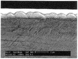
- FIG. 2 shows that a copper alloy strip according to the present invention having a configuration of a pure Sn layer, a Cu—Sn compound layer, and a copper alloy base material layer is disposed on a Fe plate having an Ni plating layer on the upper surface, and welded.
- FIG. 3 is a cross-sectional photograph (FE-SEM image) after being processed. In the welded portion (X in FIG. 2), the pure Sn layer remaining in the surrounding R (right) and L (left) is thinned or disappeared, and the Cu—Sn compound layer existing below the copper alloy strip It seems that the Ni plating on the surface of the battery electrode is directly welded (see FIG. 2).
- the welding mechanism of the copper alloy strip of the present invention is that the Sn-plated pure Sn layer that existed between the copper alloy surface of the tab and the Ni surface of the battery electrode surface first. (Melting point 230 ° C.) is melted by Joule heat generated by resistance welding, and molten Sn moves from the pressurizing part to the non-pressurizing part under pressure of the welding electrode rod. Then, the Cu—Sn compound layer (melting point: 800 ° C. or more) existing inside the pure Sn layer comes into contact with Ni as an active new surface, and is further heated and pressurized to each other (Cu—Sn compound). And Ni element) diffuse and are considered to be firmly joined.
- the Cu—Sn compound layer on the surface of the alloy strip and the Ni layer on the surface of the battery electrode are reacted and welded, and the presence of the Cu—Sn compound layer of reflow Sn plating provides excellent weldability. It is essential to achieve this. Further, considering the above mechanism and the effect of Zn addition, in order to protect the new surface of the Cu—Sn compound layer until just before the welding process, the surface pure Sn layer can be formed as much as possible without the diffusion layer growing up to the surface layer inside the Sn plating. It is desirable to exist for a long time. And since the copper alloy of this invention contains Zn, the diffusion rate of Cu is low and a pure Sn layer can exist for a long period of time.
- the copper alloy of the present invention is subjected to reflow Sn plating having a thickness of 0.20 to 3.50 ⁇ m.
- the reflow Sn plating with a thickness of 0.20 to 3.50 ⁇ m is a plating in which the total thickness of the Sn layer remaining after the reflow process and the Cu—Sn compound layer formed by the reflow process is 0.20 to 3.50 ⁇ m. .
- the thickness of the Sn layer is 0.10 to 1.60 ⁇ m, preferably 0.30 to 1.20 ⁇ m, more preferably 0.50 to 1.00 ⁇ m.
- the thickness of the Cu—Sn compound layer is 0.10 to 1.90 ⁇ m, preferably 0.20 to 1.50 ⁇ m, and more preferably 0.40 to 0.90 ⁇ m.
- the plurality of batteries welded to the tab is a battery set composed of a plurality of batteries.
- the tab portion is further welded to the base (through-hole mounting), but if the Sn layer is thin, the base is welded.
- the solder wettability at the time also worsens.
- it exceeds 1.60 ⁇ m a large amount of Sn melts at the time of welding, which makes it difficult to weld the Cu—Sn compound layer and the Ni-plated battery electrode or the Ni battery electrode under predetermined conditions that are usually employed. .
- the Cu—Sn compound layer thickness is less than 0.10 ⁇ m, it is difficult to achieve uniform welding with the electrode surface, and it is difficult to obtain the desired welding strength.
- the thickness of the Cu—Sn compound layer exceeds 1.90 ⁇ m, the thickness of the Sn plating tends to be non-uniform, resulting in a manufacturing problem. Further, the non-uniform Sn plating thickness makes it difficult to weld the Cu—Sn compound layer and the Ni-plated battery electrode or Ni battery electrode under predetermined conditions that are usually employed.
- Cu plating is usually performed on the copper alloy so as to have a thickness of 0.05 to 3.0 ⁇ m, preferably 0.1 to 1.0 ⁇ m. . Thereafter, Sn plating is performed to a thickness of 0.20 to 3.00 ⁇ m, preferably 0.23 to 2.60 ⁇ m, and then reflow treatment is performed.
- a sample is inserted into a heating furnace at a temperature of 300 to 600 ° C. and nitrogen (oxygen 1 vol% or less) for 5 to 15 seconds and then cooled with water.
- the aspect ratio b / a of the crystal grains in the plate thickness direction b and the rolling parallel direction a in the final product is 0.1 or more, preferably 0.17 to 0.75, and more preferably 0.30 to 0.70.
- FIG. 3 is a schematic diagram of crystal grains observed in the sample cross section. If the aspect ratio b / a of the crystal grains in the plate thickness direction and the rolling parallel direction is less than 0.1, the strength of the material is high, but strain is concentrated locally during repeated bending, and a shear band is easily formed. Inferior to sex.
- the average crystal grain size of the present invention is preferably 12 ⁇ m or less, more preferably 7 ⁇ m or less. If it is 12 ⁇ m or less, an increase in strength is expected, which is preferable.
- the manufacturing process of the copper alloy of the present invention is basically the same as that of a normal alloy strip, and after multiple casting, homogenization annealing and hot rolling, face milling, and cold rolling a plurality of times. It is manufactured by repeating annealing. By adjusting the following manufacturing conditions, the bendability can be further improved repeatedly.
- the end temperature of hot rolling is preferably 600 to 750 ° C.
- the degree of cold rolling after the final annealing of the product is usually 10 to 70%, preferably 10 to 60%. When these are out of the range, the aspect ratio of the crystal grains is out of the preferred range in the present invention, the bendability is repeatedly deteriorated, and the strength is insufficient.
- the intermediate annealing temperature is preferably 680 to 780 ° C. for 5 to 20 seconds, and if the annealing condition is outside the above range, the aspect ratio is outside the preferable range in the present invention, and the repeated bendability deteriorates.
- the copper alloy strip of the present invention can be welded to any material as long as it is a commonly used electrode material for a rechargeable battery, but is preferably a metal plate having a nickel plating layer on its surface, for example, nickel plated Examples include stainless steel plates, mild steel plates, and nickel plates. When a nickel plate is used for the electrode, nickel plating is not necessary.
- the thickness of the electrode material is usually 0.1 to 0.3 mm, but can vary depending on the actually used rechargeable battery and is not particularly limited.
- the welding of the tab material is performed by heat generated by the resistance between the tab plate and the electrode, and the welding quality is affected by the welding current, the energization time, and the pressing pressure.
- the welding current varies depending on the material and surface state of the member to be welded and the electrode pressing pressure. In consideration of various factors such as prevention of welding of the welder electrode, the current, the pressing pressure of the electrode, and the like can be appropriately adjusted within a range that is normally performed.
- the measurement conditions performed in the examples are as follows.
- [Measurement of plating thickness by electrolytic film thickness meter] Using a CT-1 type electrolytic film thickness meter (manufactured by Denso Co., Ltd.), the thickness of the Sn plating layer, the Cu—Sn compound layer and the Ni plating layer was measured according to JIS H8501 for the sample after reflow.
- an electrolytic solution for the Sn plating layer and the Cu—Sn compound layer an electrolytic solution R-50 (trade name) manufactured by Kocourt was used.
- an electrolyte solution R-54 (trade name) manufactured by Kocourt was used.
- the repeatable bendability is “good” ⁇ , if it is 1.5 times or more and less than 2.5 times, “within standard” ⁇ , if it is less than 1.5 times, “bad” ⁇ It was evaluated.
- a tensile test (test speed: 10 mm / min) was performed with a precision load measuring machine (MODEL-1310VR: product name) manufactured by Aiko Engineering Co., Ltd., and the welding strength was measured. If the weld strength is 35N or more, the weldability is judged as “best” (A). If the weld strength is less than 35N and 25N or more, “Better” (B), and if the weld strength is less than 25N and 20N or more, “good”. (C), “bad” (D) when the welding strength was less than 20 N, and “weld impossible” (E) when welding was not possible or stable production could not be expected.
- MODEL-1310VR product name
- the crystal grain size of the cross section parallel to the rolling direction and the cross section perpendicular to the rolling direction was measured and calculated according to the cutting method of JISH0501.
- the crystal grain size in the direction parallel to the rolling surface was measured, and the measured value in the parallel direction was the major axis a, and the measured value in the plate thickness direction was the minor axis b.
- Example preparation After electrolytic copper was melted in a high frequency induction furnace and the surface of the molten metal was coated with charcoal, an alloy element was added to adjust the molten metal to a desired composition.
- the composition of alloy elements other than copper is described in Tables 1 and 2 described later.
- the balance of the alloy is copper. Casting was performed at a casting temperature of 1200 ° C., and the obtained ingot was heated at 850 ° C. for 3 hours, and then hot rolled to a plate thickness of 8 mm, and the hot rolling end temperature was adjusted to 650 ° C. or higher. The oxidized scale formed on the surface was removed by chamfering.
- the obtained copper alloy strip was pickled with a 10% by mass sulfuric acid-1% by mass hydrogen peroxide solution to remove the surface oxide film.
- Electrolytic degreasing was performed using a sample as a cathode in an alkaline aqueous solution (current density: 7.5 A / dm 2.
- Degreasing agent sodium hydroxide 10 g / L, sodium carbonate 30 g / L, sodium metasilicate 7 g / L, balance water. Temperature: 80 ° C., time 60 seconds). It pickled using 10 mass% sulfuric acid aqueous solution.
- Cu plating plating bath composition: sulfuric acid 60 g / L, copper sulfate 200 g / L, remaining water.
- Plating bath temperature 25 ° C., current density: 5.0 A / dm 2
- Sn plating was further applied ( Plating bath composition: sulfuric acid first tin 40 g / L, sulfuric acid 60 g / L, cresolsulfonic acid 40 g / L, gelatin 2 g / L, ⁇ -naphthol 1 g / L, remaining water Plating bath temperature: 20 ° C. Current density: 1 .5 A / dm 2 ).
- the Sn plating thickness was adjusted by the electrodeposition time (when the electrodeposition time is 2 minutes, the thickness of the Sn layer before the reflow treatment is about 1 ⁇ m).
- Example 7 As a reflow treatment, the sample was inserted in a heating furnace adjusted to 400 ° C. and the atmosphere gas to nitrogen (oxygen 1 vol% or less) for 5 to 30 seconds and cooled with water. Table 1 shows the test results.
- Ni plating was performed before Cu plating under the following conditions.
- Plating bath composition nickel sulfate 250 g / L, nickel chloride 45 g / L, boric acid 30 g / L.
- Plating bath temperature 50 ° C.
- Current density 5 A / dm 2 .
- the Ni plating thickness was adjusted to 0.30 ⁇ m by the electrodeposition time.
- Example 11 it prepared on the same conditions as Example 9 except not performing Cu plating.
- Examples 1 to 25 in Table 1 are within the scope of the present invention, they were alloy strips having tensile strength, conductivity, repeated bendability, weldability and recyclability that were good or within specifications.
- Example 11 without Cu plating the copper alloy base material reacted with the Sn plating layer by the reflow treatment to form a Cu—Sn compound layer having a thickness of 0.70 ⁇ m.
- the Zn concentration was about 10% and the Sn concentration was about 0.5%, so that the conductivity was relatively low, about 32% IACS.
- Example 3 the cold rolling workability after the final annealing exceeded 70% and the aspect ratio was low within the range of the present invention, but the repeated bendability was within the specification.
- Example 18 the degree of processing was less than 10% and the aspect ratio was 0.78, but no significant reduction in strength was observed.
- Example 19 with a workability of 15% the aspect ratio was 0.71, and sufficient strength was maintained.
- Comparative Example 26 was commercially pure copper, the tensile strength was inferior, and the electrical conductivity was extremely high, so the amount of heat generated during welding was small and welding was impossible. In addition, a refining process is required to recycle the Sn plated end material as a raw material, and the recyclability is also poor. Comparative Examples 27 and 28 are Ni plates that have been used in the past, and the recyclability of the Sn-plated Ni plate itself is good, but the battery performance cannot be improved because of poor conductivity. When Sn plating is performed, the recyclability becomes poor. Since Comparative Example 27 has a low degree of processing, the aspect ratio is high, and the strength is lower than that of Comparative Example 28.
- Comparative Examples 29 to 31 are Corson alloy-based copper alloys that do not contain Zn and are all unweldable. Since Comparative Example 29 does not contain Sn, it has lower strength than Comparative Example 30 and is inferior in recyclability. Increased tensile strength results in poor repeatability. Since Comparative Example 32 did not contain Zn and Sn and contained Mg, there was no decrease in strength, but welding was impossible and recyclability was poor. Comparative Example 33 does not contain Zn, the Sn concentration exceeds the upper limit of the present invention, the electrical conductivity is low, and the repeated bendability is also poor.
- Comparative Example 34 is an example of a precipitation hardening type copper alloy that contains a small amount of Zn, does not contain Sn, and contains Fe and a small amount of P. Although there was no decrease in strength, the welding rod was corroded and could not be welded. Also, recyclability is bad. Since the Zn concentrations of Comparative Examples 35 and 36 were less than 2%, the strength was relatively low, the conductivity was too high, and welding was poor. Moreover, since the comparative example 35 has low Sn density
- Comparative Examples 38, 40, and 41 were within the scope of the present invention, the pure Sn layer thickness during Sn plating was small, resulting in poor welding.
- Comparative Example 39 the thickness of the pure Sn layer was large, and Sn could not be welded because a large amount of Sn melted during welding.
- the Zn concentration and Sn concentration of Comparative Example 42 were within the scope of the present invention, the thickness of the Cu—Sn compound layer was small, the tensile strength was small, and welding was poor.
- Comparative Example 43 the Zn concentration and Sn concentration, and the layer thickness after reflowing are within the range of the present invention, but the tensile strength is increased, but the workability is high and the aspect ratio of the crystal grains is outside the range of the present invention. The strength is high, but the repeated bendability is poor. Since the Sn concentration of Comparative Example 44 exceeds 0.8%, the electrical conductivity is low and the repeated bendability and recyclability are poor. In Comparative Examples 45 to 48, the Zn concentration exceeds 12%, so the conductivity is low, Zn vaporizes during welding, and the weld becomes brittle.
- Comparative Example 48 is a general commercial brass having a high Zn concentration, and the aspect ratio is high because the degree of processing is relatively low, but the strength is ensured because of a material that is easy to work and harden. However, since Sn is not included, it is inferior in recyclability. As mentioned above, although this invention aims at the outstanding effect balanced in all the items of tensile strength, electrical conductivity, repeated bendability, and weldability, the effect was not able to be achieved in the comparative example.
- the copper alloy strip of the present invention has a good balance of tensile strength, electrical conductivity, repeated bendability and weldability, and a battery tab material for charging, in particular, a high-performance charging battery such as a Li-ion battery. It can use suitably for the tab material to connect.
Landscapes
- Chemical & Material Sciences (AREA)
- Chemical Kinetics & Catalysis (AREA)
- Electrochemistry (AREA)
- Organic Chemistry (AREA)
- Engineering & Computer Science (AREA)
- Materials Engineering (AREA)
- Metallurgy (AREA)
- General Chemical & Material Sciences (AREA)
- Mechanical Engineering (AREA)
- Physics & Mathematics (AREA)
- Thermal Sciences (AREA)
- Crystallography & Structural Chemistry (AREA)
- Connection Of Batteries Or Terminals (AREA)
- Electroplating Methods And Accessories (AREA)
- Sealing Battery Cases Or Jackets (AREA)
Abstract
本発明は、良好な引張り強さ、導電率、繰り返し曲げ性及び溶接性をバランス良く兼ね備えた電池接続タブ材に好適な銅合金条を目的とする。本発明は、2~12質量%のZnを含有し、かつ0.1~1.5質量%のSnを含有し、残部が銅及び不可避的不純物から成る銅合金条であって、板厚方向及び圧延平行方向の結晶粒のアスペクト比が0.1以上であり、リフロー後のSn層の厚みが0.10~1.60μmであり、かつCu-Sn化合物の厚みが0.10~1.90μmであるリフローSnめっきが施されている、充電用電池タブ用のSnめっき銅合金条に関する。この銅合金条は好ましくは、Ni/Cu下地めっき又はCu下地めっきが施されており、導電率が31~70%IACSであり、180°密着曲げ及び曲げ戻し試験での繰り返し曲げ回数が2.5回以上であり、引張り強さが300~610MPaである。
Description
本発明は、充電用電池タブ材、詳細にはLiイオン電池等の高性能充電用電池を接続するタブ材に用いられる銅合金条に関する。
ビデオカメラやラップトップコンピュータ等の携帯用電子機器にはニッカド電池やLiイオン電池等の充電式電池が用いられる。また、近年の環境負荷低減の動きを受け、電気自動車やハイブリッド自動車の需要も増加し、車載用Liイオン二次電池の開発も進んでいる。これら充電式電池は必要な電気容量を確保するため、複数個の単体構造の電池を複数本互いに近接した状態で電気的に接続して使用される。電池の接続に用いられる金属リード材料は、集電タブ又はタブと呼ばれ、確実に接続するために、電気抵抗による発熱を利用した抵抗溶接により電池の電極と溶着されることが多い。電極にタブが溶接された複数個の電池はコンパクトなケース内に収納されるが、小型化、複雑化されたケース等への収納に失敗した場合等、ケースから電池を出し入れする際、再度タブの曲げ戻し及び曲げ加工が必要であり、タブに使用される材料には電極材料との良好な溶接性だけでなく繰り返し曲げ性も要求される。
電池電極材料には、通常、ニッケルめっきされたステンレス板や軟鋼板、又はニッケル板が使用されてきた。抵抗溶接機を用いて、これら材料板からなる電池電極とタブを接続する際、銅は導電率が高すぎるため、タブに過大な電流が流れ溶損に至る欠点を有することから実用化されておらず、従来のタブ材料には比較的溶接溶着性の良いニッケル条が使用されていた。しかし、ニッケルは希少金属であり価格が非常に高く供給が不安定となる危険性もある。またニッケルの導電率は21.5%IACS(実測値)と比較的低いため、高容量電池での使用中に発熱しやすい欠点がある。そのため、コストダウン及び電池高性能化を求めて、ニッケルを他の金属材料で代替する要求がある。現在、銅地金の価格はニッケルの約3分の1程度と魅力的であるが、様々な公知の銅合金をタブ材料として使用しても溶接が困難であったため、実際にはほとんど利用されていなかった。また、銅又は耐熱銅合金基層と、Ni等からなる溶接層とのクラッドを用い、溶接性の改良を行なう試みがなされたが(特開平11-297300)、銅は強度が低く、上記耐熱銅合金も、繰り返し曲げ加工性が悪く小型化のニーズには対応できなかった。
本発明は、良好な引張り強さ、導電率、繰り返し曲げ性及び溶接性をバランス良く兼ね備えた電池接続タブ材に好適な銅合金条を目的とする。
本発明は、リフローSnめっきされたCu-Zn系銅合金が、良好な引張り強さ、導電率、繰り返し曲げ性及び溶接性を有する電池用タブ材に好適であることを発見してなされたものであり、具体的には、下記のとおりである。
(1) 2~12質量%のZnを含有し、かつ0.1~1.5質量%のSnを含有し、残部が銅及び不可避的不純物から成る銅合金条であって、板厚方向及び圧延平行方向の結晶粒のアスペクト比が0.1以上であり、リフロー後のSn層の厚みが0.10~1.60μmであり、かつCu-Sn化合物の厚みが0.10~1.90μmであるリフローSnめっきが施されている、充電用電池タブ用のSnめっき銅合金条。
(2) Ni/Cu下地めっき又はCu下地めっきが施されている上記(1)に記載のSnめっき銅合金条。
(3) 導電率が31~70%IACSである上記(1)又は(2)に記載の銅合金条。
(4) 180°密着曲げ及び曲げ戻し試験での繰り返し曲げ回数が2.5回以上である上記(1)~(3)いずれかに記載の銅合金条。
(5) 引張り強さが300~610MPaである上記(1)~(4)いずれかに記載の銅合金条。
(1) 2~12質量%のZnを含有し、かつ0.1~1.5質量%のSnを含有し、残部が銅及び不可避的不純物から成る銅合金条であって、板厚方向及び圧延平行方向の結晶粒のアスペクト比が0.1以上であり、リフロー後のSn層の厚みが0.10~1.60μmであり、かつCu-Sn化合物の厚みが0.10~1.90μmであるリフローSnめっきが施されている、充電用電池タブ用のSnめっき銅合金条。
(2) Ni/Cu下地めっき又はCu下地めっきが施されている上記(1)に記載のSnめっき銅合金条。
(3) 導電率が31~70%IACSである上記(1)又は(2)に記載の銅合金条。
(4) 180°密着曲げ及び曲げ戻し試験での繰り返し曲げ回数が2.5回以上である上記(1)~(3)いずれかに記載の銅合金条。
(5) 引張り強さが300~610MPaである上記(1)~(4)いずれかに記載の銅合金条。
(銅合金)
本発明はCu-Zn-Sn系合金に関する。Cu-Zn-Sn系合金以外に高強度、高導電性を有する銅合金として代表的な銅合金は、特許文献1の段落「0021」で好ましい組成として挙げられているCu-Zr系、Cu-Cr系、Cu-Be-Co系合金や、その他Cu-Ni-Si系、Cu-Mg-P系、Cu-Ni-Sn系、Cu-Fe-P系等が挙げられる。しかし本発明者が検討した結果、これらの銅合金はいずれも、高強度、高導電性ではあるが、溶接性、繰り返し曲げ性の何れかが劣り、タブ用としては不適であることが分った。
本発明のCu-Zn-Sn系合金は、適正なZn、Sn含有量に加えて結晶粒径のアスペクト比を管理することにより、高強度、高導電性以外のタブ用材料としての特性を具備し、最適であることが分った。
本発明はCu-Zn-Sn系合金に関する。Cu-Zn-Sn系合金以外に高強度、高導電性を有する銅合金として代表的な銅合金は、特許文献1の段落「0021」で好ましい組成として挙げられているCu-Zr系、Cu-Cr系、Cu-Be-Co系合金や、その他Cu-Ni-Si系、Cu-Mg-P系、Cu-Ni-Sn系、Cu-Fe-P系等が挙げられる。しかし本発明者が検討した結果、これらの銅合金はいずれも、高強度、高導電性ではあるが、溶接性、繰り返し曲げ性の何れかが劣り、タブ用としては不適であることが分った。
本発明のCu-Zn-Sn系合金は、適正なZn、Sn含有量に加えて結晶粒径のアスペクト比を管理することにより、高強度、高導電性以外のタブ用材料としての特性を具備し、最適であることが分った。
(A)Zn濃度
本発明の合金は、2~12質量%(以下%で表す)、好ましくは2~9%のZnを含有し、残部が銅及び不可避的不純物から成る銅合金である。Zn濃度が2%未満であると、タブとして必要な強度が不充分になると共に、導電率が高くなりすぎて溶接時にタブが溶損したり、銅合金条を通過する電流により発生する発熱量が少なく、電池電極側のステンレス板や軟鋼板に電流が流れにくくなるため溶接性が劣化する。Zn濃度が12%を超えると溶接時にZnが気化して材料が脆化して溶接性が劣化するだけでなく、導電率が低くなり電池の高性能化が達成しにくい。更に、一般的にZnはCuの価格の半分以下であるためコスト削減にも効果的な添加元素であるといえる。
本発明の合金は、2~12質量%(以下%で表す)、好ましくは2~9%のZnを含有し、残部が銅及び不可避的不純物から成る銅合金である。Zn濃度が2%未満であると、タブとして必要な強度が不充分になると共に、導電率が高くなりすぎて溶接時にタブが溶損したり、銅合金条を通過する電流により発生する発熱量が少なく、電池電極側のステンレス板や軟鋼板に電流が流れにくくなるため溶接性が劣化する。Zn濃度が12%を超えると溶接時にZnが気化して材料が脆化して溶接性が劣化するだけでなく、導電率が低くなり電池の高性能化が達成しにくい。更に、一般的にZnはCuの価格の半分以下であるためコスト削減にも効果的な添加元素であるといえる。
(B)Sn濃度
Snは圧延の際の加工硬化を促進する作用を持ち、強度上昇に寄与する。本発明の銅合金条はSnリフローめっきされるので、Snめっき後の工程で発生する端材には必然的にSn成分が含まれる。しかし、本発明の銅合金条はSnを上記範囲内で含むので、Snめっき後の端材であっても本発明の銅合金原料として簡単にリサイクルできる利点がある。一方、強度上昇の為にSn以外の添加元素を採用してSnを含まない銅合金組成とした場合、Snめっき後の端材をリサイクルするためには精錬工程が必要となる。しかし、Sn濃度が低い場合は、Snめっき前に発生する端材とSnめっき後の端材とを併せて本発明の銅合金原料用スクラップとする場合、Snめっき後の端材の使用量が制限されるためマスバランスをとるのが困難になり、リサイクル性に劣る。反対にSn濃度が高いと、Snめっき前に発生する端材の使用量が制限されるため、やはりマスバランスをとるのが困難になる。従って、本発明の合金は、0.1~1.5%、好ましくは0.1~0.8%、更に好ましくは0.2~0.6%のSnを含有する。Sn濃度が0.1%未満では所望の効果が得られず、Sn濃度が1.5%を超えると導電率が低下する。
Snは圧延の際の加工硬化を促進する作用を持ち、強度上昇に寄与する。本発明の銅合金条はSnリフローめっきされるので、Snめっき後の工程で発生する端材には必然的にSn成分が含まれる。しかし、本発明の銅合金条はSnを上記範囲内で含むので、Snめっき後の端材であっても本発明の銅合金原料として簡単にリサイクルできる利点がある。一方、強度上昇の為にSn以外の添加元素を採用してSnを含まない銅合金組成とした場合、Snめっき後の端材をリサイクルするためには精錬工程が必要となる。しかし、Sn濃度が低い場合は、Snめっき前に発生する端材とSnめっき後の端材とを併せて本発明の銅合金原料用スクラップとする場合、Snめっき後の端材の使用量が制限されるためマスバランスをとるのが困難になり、リサイクル性に劣る。反対にSn濃度が高いと、Snめっき前に発生する端材の使用量が制限されるため、やはりマスバランスをとるのが困難になる。従って、本発明の合金は、0.1~1.5%、好ましくは0.1~0.8%、更に好ましくは0.2~0.6%のSnを含有する。Sn濃度が0.1%未満では所望の効果が得られず、Sn濃度が1.5%を超えると導電率が低下する。
(C)その他の元素
上記の既存の高強度、高導電性銅合金には強度その他の特性を改良するためにMg、Fe、Siが添加されることが多い。しかし、以下の理由により、本発明の合金へこれら元素が含まれる場合には注意を要する。
本発明の銅合金に活性金属であるMgが含まれる場合、溶接時にMgが気化してスパークが発生しやすく溶接が困難になると共に材料が脆化する。よって、Mg濃度は好ましくは0.3%以下、更に好ましくは0.1%以下である。
本発明の銅合金にFeが含まれる場合、溶接機の電極材(溶接棒)と反応して溶接棒が腐食されてしまい溶接性及び生産性に劣る。そして、Feは銅マトリックスに殆ど固溶しないため、Fe含有量が微量でもFeリッチ相は母相中に局在的に存在して、上記問題を発生させる。よって、Fe濃度は好ましくは0.05%以下である。
Si及びNiを含む析出型銅合金であるコルソン合金の場合、スポット抵抗溶接ができず溶接性に劣る。理論により本発明を限定するものではないが、溶接の際に発生するジュール熱で析出物が固溶し、導電率が急激に低下して溶接が困難になるとも考えられる。
上記の既存の高強度、高導電性銅合金には強度その他の特性を改良するためにMg、Fe、Siが添加されることが多い。しかし、以下の理由により、本発明の合金へこれら元素が含まれる場合には注意を要する。
本発明の銅合金に活性金属であるMgが含まれる場合、溶接時にMgが気化してスパークが発生しやすく溶接が困難になると共に材料が脆化する。よって、Mg濃度は好ましくは0.3%以下、更に好ましくは0.1%以下である。
本発明の銅合金にFeが含まれる場合、溶接機の電極材(溶接棒)と反応して溶接棒が腐食されてしまい溶接性及び生産性に劣る。そして、Feは銅マトリックスに殆ど固溶しないため、Fe含有量が微量でもFeリッチ相は母相中に局在的に存在して、上記問題を発生させる。よって、Fe濃度は好ましくは0.05%以下である。
Si及びNiを含む析出型銅合金であるコルソン合金の場合、スポット抵抗溶接ができず溶接性に劣る。理論により本発明を限定するものではないが、溶接の際に発生するジュール熱で析出物が固溶し、導電率が急激に低下して溶接が困難になるとも考えられる。
(D)合金条の特性
本発明の合金条の導電率(JIS H 0505)は、通常31~70%、好ましくは35~70%IACS、更に好ましくは40~60%IACSであり、この範囲であるとタブ材料として適切に使用できる。31%IACS未満であると充電池使用時に熱が発生しやすい。一方、70%IACSを超えると抵抗溶接時に溶損が起こったり、電池電極側の金属板に充分な電流が流れず、溶接性が低下する。
本発明の合金条の繰り返し曲げ性は、180°U字曲げ又は密着曲げの後、曲げ戻しを行なって1回のサイクルとした場合、少なくとも10mm幅の試料が破断するまでの繰り返し曲げ回数が通常2.5回以上、好ましくは3.0回以上、更に好ましくは3.5回以上である。2.5回未満であると電池をケース内に収納する操作中に破損する可能性が高く生産効率が低下する。
本発明の合金条の導電率(JIS H 0505)は、通常31~70%、好ましくは35~70%IACS、更に好ましくは40~60%IACSであり、この範囲であるとタブ材料として適切に使用できる。31%IACS未満であると充電池使用時に熱が発生しやすい。一方、70%IACSを超えると抵抗溶接時に溶損が起こったり、電池電極側の金属板に充分な電流が流れず、溶接性が低下する。
本発明の合金条の繰り返し曲げ性は、180°U字曲げ又は密着曲げの後、曲げ戻しを行なって1回のサイクルとした場合、少なくとも10mm幅の試料が破断するまでの繰り返し曲げ回数が通常2.5回以上、好ましくは3.0回以上、更に好ましくは3.5回以上である。2.5回未満であると電池をケース内に収納する操作中に破損する可能性が高く生産効率が低下する。
本発明の合金条の引張り強さ(JIS Z 2241)は、通常300~610MPa、好ましくは390~600MPa、更に好ましくは390~540MPaであるとタブ材料として好適に使用できる。610MPaを超える場合は、通常、繰り返し曲げ性に劣る。また、引張り強さが300MPa未満では、通常、Liイオン電池用タブに求められる耐振動性基準を満たさない。
本発明の合金条の厚みは特に限定はされないが好ましくは0.03~1.00mm、より好ましくは0.12~0.6mmであり、例えば0.15mmであり、この厚さであると充電池接続用タブ材料としての強度、溶接性を満たす。
本発明の合金条の厚みは特に限定はされないが好ましくは0.03~1.00mm、より好ましくは0.12~0.6mmであり、例えば0.15mmであり、この厚さであると充電池接続用タブ材料としての強度、溶接性を満たす。
(E-1)Cu下地リフローSnめっき
本発明の銅合金条には0.20~3.50μm(リフロー処理後のSn層及びCu-Sn化合物層の合計厚み)のリフローSnめっきが施されて、優れた溶接性を達成している。リフローSnめっきは、銅合金母材上に、電気めっき等によりCu下地めっき層の上にSnめっき層を形成し、リフロー処理を行って形成される。このリフロー処理により、銅合金母材及びCu下地めっき層がSnめっき層と反応してCu-Sn化合物層(CuがSnめっき層へ拡散して形成されるため拡散層ともいう)が形成され、めっき層構造は、表面側より純Sn層、Cu-Sn化合物層、Cuめっき層、母材層となる(図1参照)。また、Cuめっき層はリフロー後にCu-Sn化合物へ完全に転換されてもよく、残存しても良い。なお、本発明ではCuめっき層の厚みによる溶接性への影響は殆ど認められず、リフロー処理前のCu下地めっき層の厚みは特に限定はされないが好ましくは0.05~3.0μm、より好ましくは0.1~1.0μmである。また、Cu下地めっきを行わなくても良い。
本発明の銅合金条には0.20~3.50μm(リフロー処理後のSn層及びCu-Sn化合物層の合計厚み)のリフローSnめっきが施されて、優れた溶接性を達成している。リフローSnめっきは、銅合金母材上に、電気めっき等によりCu下地めっき層の上にSnめっき層を形成し、リフロー処理を行って形成される。このリフロー処理により、銅合金母材及びCu下地めっき層がSnめっき層と反応してCu-Sn化合物層(CuがSnめっき層へ拡散して形成されるため拡散層ともいう)が形成され、めっき層構造は、表面側より純Sn層、Cu-Sn化合物層、Cuめっき層、母材層となる(図1参照)。また、Cuめっき層はリフロー後にCu-Sn化合物へ完全に転換されてもよく、残存しても良い。なお、本発明ではCuめっき層の厚みによる溶接性への影響は殆ど認められず、リフロー処理前のCu下地めっき層の厚みは特に限定はされないが好ましくは0.05~3.0μm、より好ましくは0.1~1.0μmである。また、Cu下地めっきを行わなくても良い。
(E-2)Ni/Cu下地リフローSnめっき
溶接性にはCu-Sn化合物層及びリフロー後の純Sn層の合計厚みが関与するため、めっきの耐熱性を向上させる目的で、上記Cuめっきを行う前にNiめっきを施しても良い。
Ni/Cu下地リフローSnめっきは母材上に、電気めっきによりNiめっき層、Cuめっき層及びSnめっき層を順次形成し、その後リフロー処理を行う。このリフロー処理により、めっき層間のCuとSnが反応してCu-Sn化合物層が形成される。一方Niめっき層は、ほぼ電気めっき上がりの状態(厚み)で残留する。リフロー処理後のめっき層の構造は、表面側よりSnめっき層、Cu-Sn化合物層、Niめっき層となる。Ni下地めっき層の厚みは特に限定はされないが好ましくは0.1~0.8μm、より好ましくは0.1~0.3μmである。その他のめっき条件は(E-1)と同等である。
溶接性にはCu-Sn化合物層及びリフロー後の純Sn層の合計厚みが関与するため、めっきの耐熱性を向上させる目的で、上記Cuめっきを行う前にNiめっきを施しても良い。
Ni/Cu下地リフローSnめっきは母材上に、電気めっきによりNiめっき層、Cuめっき層及びSnめっき層を順次形成し、その後リフロー処理を行う。このリフロー処理により、めっき層間のCuとSnが反応してCu-Sn化合物層が形成される。一方Niめっき層は、ほぼ電気めっき上がりの状態(厚み)で残留する。リフロー処理後のめっき層の構造は、表面側よりSnめっき層、Cu-Sn化合物層、Niめっき層となる。Ni下地めっき層の厚みは特に限定はされないが好ましくは0.1~0.8μm、より好ましくは0.1~0.3μmである。その他のめっき条件は(E-1)と同等である。
図2は、Niめっき層を上表面に設けたFe板上に、下から純Sn層、Cu-Sn化合物層、銅合金母材層の構成を有する本発明の銅合金条が配置され、溶着された後の断面写真(FE-SEM像)である。溶着箇所(図2のX)では、周囲R(右)及びL(左)に残っている純Sn層が薄くなるか消滅しており、銅合金条の下部に存在するCu-Sn化合物層と電池電極表面のNiめっきが直接溶着されているように見える(図2参照)。理論によって本発明を制限するものではないが、本発明の銅合金条の溶着メカニズムは、まず、タブの銅合金表面と電池電極表面のNi面の間に存在していたSnめっきの純Sn層(融点230℃)が抵抗溶接によって発生したジュール熱で溶融し、溶接用電極棒の加圧下では溶融Snが加圧部から非加圧部まで移動する。すると純Sn層よりも内部に存在していたCu-Sn化合物層(融点800℃以上)が活性な新生面としてNiと接触し、更に加熱加圧されることにより相互に各成分(Cu-Sn化合物及びNi元素)が拡散し強固に接合すると考えられる。従って、溶接後のタブでは、合金条表面のCu-Sn化合物層と電池電極表面のNi層が反応して溶着しており、リフローSnめっきのCu-Sn化合物層の存在は優れた溶接性を達成するために必須であるといえる。
また、上記メカニズムとZnの添加効果を考察すると、Cu-Sn化合物層の新生面を溶接工程直前まで保護するためには、Snめっき内部で拡散層が表層まで成長せずに表面純Sn層ができるだけ長く存在することが望ましい。そして本願発明の銅合金にはZnが含まれるためCuの拡散速度が低く、純Sn層が長期間存在することができる。
また、上記メカニズムとZnの添加効果を考察すると、Cu-Sn化合物層の新生面を溶接工程直前まで保護するためには、Snめっき内部で拡散層が表層まで成長せずに表面純Sn層ができるだけ長く存在することが望ましい。そして本願発明の銅合金にはZnが含まれるためCuの拡散速度が低く、純Sn層が長期間存在することができる。
本発明の銅合金には厚み0.20~3.50μmのリフローSnめっきが施されている。厚み0.20~3.50μmのリフローSnめっきとは、リフロー処理後に残存するSn層及びリフロー処理により形成されるCu-Sn化合物層の厚み合計が0.20~3.50μmであるめっきである。Sn層の厚みは0.10~1.60μm、好ましくは0.30~1.20μm、更に好ましくは0.50~1.00μmである。Cu-Sn化合物層の厚みは0.10~1.90μm、好ましくは0.20~1.50μm、更に好ましくは0.40~0.90μmである。
Sn層厚みが0.10μm未満になると電池電極板との溶接時にCu-Sn化合物層の新生面が得られにくく溶接性が劣る。また、タブに溶着された複数個の電池は、複数個の電池から構成される電池セットとなり、タブ部は更に基盤と溶接(スルーホール実装)されるが、Sn層が薄いと基盤との溶接時の半田濡れ性も悪くなる。一方、1.60μmを超えると溶接時にSnが多量に溶融するため、Cu-Sn化合物層とNiめっきされた電池電極又はNi電池電極との溶着が通常採用される所定の条件下で困難になる。
Cu-Sn化合物層厚みが0.10μm未満であると電極表面との均一な溶着が困難であるため目的とする溶接強度が得られにくい。一方、Cu-Sn化合物層の厚みが1.90μmを超えると、Snめっきの厚みが不均一になりやすく、製造上支障が生じる。また、Snめっきの厚みが不均一となることにより、Cu-Sn化合物層とNiめっきされた電池電極又はNi電池電極との溶着が通常採用される所定の条件下で困難になる。
Sn層厚みが0.10μm未満になると電池電極板との溶接時にCu-Sn化合物層の新生面が得られにくく溶接性が劣る。また、タブに溶着された複数個の電池は、複数個の電池から構成される電池セットとなり、タブ部は更に基盤と溶接(スルーホール実装)されるが、Sn層が薄いと基盤との溶接時の半田濡れ性も悪くなる。一方、1.60μmを超えると溶接時にSnが多量に溶融するため、Cu-Sn化合物層とNiめっきされた電池電極又はNi電池電極との溶着が通常採用される所定の条件下で困難になる。
Cu-Sn化合物層厚みが0.10μm未満であると電極表面との均一な溶着が困難であるため目的とする溶接強度が得られにくい。一方、Cu-Sn化合物層の厚みが1.90μmを超えると、Snめっきの厚みが不均一になりやすく、製造上支障が生じる。また、Snめっきの厚みが不均一となることにより、Cu-Sn化合物層とNiめっきされた電池電極又はNi電池電極との溶着が通常採用される所定の条件下で困難になる。
0.20~3.50μmのリフローSnめっきを形成するには、通常は0.05~3.0μm、好ましくは0.1~1.0μmの厚みとなるように銅合金上にCuめっきを行う。その後、0.20~3.00μm、好ましくは0.23~2.60μmの厚みとなるようにSnめっきを行った後、リフロー処理をする。通常のリフロー処理は、温度を300~600℃、窒素(酸素1vol%以下)雰囲気の加熱炉中に、試料を5~15秒間挿入した後水冷する。
(F)結晶粒のアスペクト比
結晶粒のアスペクト比を調整すると、繰り返し曲げ性をさらに改善することができる。最終製品における板厚方向b及び圧延平行方向aの結晶粒のアスペクト比b/aは0.1以上、好ましくは0.17~0.75、更に好ましくは0.30~0.70である。図3は試料断面にて観察される結晶粒の模式図である。
板厚方向及び圧延平行方向の結晶粒のアスペクト比b/aが0.1未満では、材料の強度は高いが、繰り返し曲げ時にひずみが局部的に集中してせん断帯が形成されやすく、繰り返し曲げ性に劣る。b/aが0.80を超えると繰り返し曲げ性は良好であるが、低い加工度で製造されるため、強度が低く、タブ材料として使用中に振動や衝撃で破断する恐れがある。
本発明の平均結晶粒径は、好ましくは12μm以下、更に好ましくは7μm以下である。12μm以下であると、強度の増加が見込まれるので好ましい。
結晶粒のアスペクト比を調整すると、繰り返し曲げ性をさらに改善することができる。最終製品における板厚方向b及び圧延平行方向aの結晶粒のアスペクト比b/aは0.1以上、好ましくは0.17~0.75、更に好ましくは0.30~0.70である。図3は試料断面にて観察される結晶粒の模式図である。
板厚方向及び圧延平行方向の結晶粒のアスペクト比b/aが0.1未満では、材料の強度は高いが、繰り返し曲げ時にひずみが局部的に集中してせん断帯が形成されやすく、繰り返し曲げ性に劣る。b/aが0.80を超えると繰り返し曲げ性は良好であるが、低い加工度で製造されるため、強度が低く、タブ材料として使用中に振動や衝撃で破断する恐れがある。
本発明の平均結晶粒径は、好ましくは12μm以下、更に好ましくは7μm以下である。12μm以下であると、強度の増加が見込まれるので好ましい。
(G)製造方法
本発明の銅合金の製造工程は、基本的には通常の合金条と同様であり、溶解鋳造、均質化焼鈍及び熱間圧延、面削の後、複数回の冷間圧延、焼鈍を繰り返し、製造される。
以下の製造条件を調整する事で、さらに繰り返し曲げ性を改善する事が出来る。
熱間圧延の終了温度は好ましくは600~750℃であり、製品の最終焼鈍後の冷間圧延の加工度は通常10~70%、好ましくは10~60%である。これらが範囲外であると結晶粒のアスペクト比が本発明で好ましい範囲外となり、繰り返し曲げ性が劣化し、強度も不足する。
中間焼鈍温度は好ましくは680~780℃で5~20秒であり、焼鈍条件が前述の範囲外であると、アスペクト比が本発明で好ましい範囲外となり、繰り返し曲げ性が劣化する。
本発明の銅合金の製造工程は、基本的には通常の合金条と同様であり、溶解鋳造、均質化焼鈍及び熱間圧延、面削の後、複数回の冷間圧延、焼鈍を繰り返し、製造される。
以下の製造条件を調整する事で、さらに繰り返し曲げ性を改善する事が出来る。
熱間圧延の終了温度は好ましくは600~750℃であり、製品の最終焼鈍後の冷間圧延の加工度は通常10~70%、好ましくは10~60%である。これらが範囲外であると結晶粒のアスペクト比が本発明で好ましい範囲外となり、繰り返し曲げ性が劣化し、強度も不足する。
中間焼鈍温度は好ましくは680~780℃で5~20秒であり、焼鈍条件が前述の範囲外であると、アスペクト比が本発明で好ましい範囲外となり、繰り返し曲げ性が劣化する。
(H)溶接条件
本発明の銅合金条は、通常使用される充電池の電極材料であればどの材料にも溶接できるが、好ましくはニッケルめっき層を表面に有する金属板、例えばニッケルめっきされたステンレス板や軟鋼板、更にはニッケル板が挙げられる。なお、ニッケル板を電極に使用する場合はニッケルめっき不要である。電極材料厚みは通常0.1~0.3mmであるが、実際に使用される充電池に応じて変動可能であり特に制限されない。
タブ材の溶接は、タブ板と電極間の抵抗による発熱で行われ、溶接品質は、溶接電流・通電時間・押下圧力の影響を受ける。溶接電流は、溶接する部材の材質及び表面状態、並びに電極押下圧力により変化する。そして、溶接機電極の溶着を防止する等、種々の要素を考慮して、電流や電極の押下圧力などを通常行われる範囲内で適宜調整できる。
本発明の銅合金条は、通常使用される充電池の電極材料であればどの材料にも溶接できるが、好ましくはニッケルめっき層を表面に有する金属板、例えばニッケルめっきされたステンレス板や軟鋼板、更にはニッケル板が挙げられる。なお、ニッケル板を電極に使用する場合はニッケルめっき不要である。電極材料厚みは通常0.1~0.3mmであるが、実際に使用される充電池に応じて変動可能であり特に制限されない。
タブ材の溶接は、タブ板と電極間の抵抗による発熱で行われ、溶接品質は、溶接電流・通電時間・押下圧力の影響を受ける。溶接電流は、溶接する部材の材質及び表面状態、並びに電極押下圧力により変化する。そして、溶接機電極の溶着を防止する等、種々の要素を考慮して、電流や電極の押下圧力などを通常行われる範囲内で適宜調整できる。
実施例で行った測定の条件は下記の通りである。
[電解式膜厚計によるめっき厚測定]
CT-1型電解式膜厚計(株式会社電測製)を用い、リフロー後の試料に対し、JIS H8501に従い、Snめっき層、Cu-Sn化合物層及びNiめっき層の厚みを測定した。Snめっき層及びCu-Sn化合物層に対する電解液は、コクール社製電解液 R-50(商品名)を使用した。また、Niめっき層に対しては、コクール社製電解液 R-54(商品名)を使用した。
[導電率]
各銅合金板について、JISH0505に準拠し、ダブルブリッジ装置を用いた四端子法により求めた体積抵抗率から%IACSを算出した。導電率が40%以上なら導電性が「良好」○、31%以上40%未満又はであれば「規格内」△、31%未満の場合は「不良」×と評価した。
[電解式膜厚計によるめっき厚測定]
CT-1型電解式膜厚計(株式会社電測製)を用い、リフロー後の試料に対し、JIS H8501に従い、Snめっき層、Cu-Sn化合物層及びNiめっき層の厚みを測定した。Snめっき層及びCu-Sn化合物層に対する電解液は、コクール社製電解液 R-50(商品名)を使用した。また、Niめっき層に対しては、コクール社製電解液 R-54(商品名)を使用した。
[導電率]
各銅合金板について、JISH0505に準拠し、ダブルブリッジ装置を用いた四端子法により求めた体積抵抗率から%IACSを算出した。導電率が40%以上なら導電性が「良好」○、31%以上40%未満又はであれば「規格内」△、31%未満の場合は「不良」×と評価した。
[引張り強さ]
各銅合金板について、圧延方向に平行な方向に引張試験を行ない、JISZ2241に準拠して求めた。
[繰り返し曲げ性]
長手方向が圧延方向に平行となる様に、厚さ0.15mm、幅10mm、長さ40mmの最終品試験片を4個作製し、試験片の長手方向に直角な方向を曲げ軸として、180°密着曲げを行なった後、曲げ戻した。これを1回として、試料が破断するまで繰り返し曲げを行い、試料4個の平均破断(繰り返し曲げ)回数を求めた。平均破断回数が2.5回以上なら繰り返し曲げ性が「良好」○、1.5回以上2.5回未満であれば「規格内」△、1.5回未満の場合は「不良」×と評価した。
各銅合金板について、圧延方向に平行な方向に引張試験を行ない、JISZ2241に準拠して求めた。
[繰り返し曲げ性]
長手方向が圧延方向に平行となる様に、厚さ0.15mm、幅10mm、長さ40mmの最終品試験片を4個作製し、試験片の長手方向に直角な方向を曲げ軸として、180°密着曲げを行なった後、曲げ戻した。これを1回として、試料が破断するまで繰り返し曲げを行い、試料4個の平均破断(繰り返し曲げ)回数を求めた。平均破断回数が2.5回以上なら繰り返し曲げ性が「良好」○、1.5回以上2.5回未満であれば「規格内」△、1.5回未満の場合は「不良」×と評価した。
[溶接性]
シリーズスポット溶接機(例えば、ミヤチテクノス製トランジスタ式抵抗溶接電源MDB-4000B(製品名)及びエア駆動式ヘッドZH-32(製品名))にて加圧力20N、溶接電流3.0kA、溶接時間10msecにて、厚み3.0μmのNiめっきを施した0.3mmの軟鋼板(JIS G3101規格)と本発明の銅合金試験片を2点でスポット溶接した(電極間隔は、10~50mmの範囲内であれば特に問題なく同様に溶接可能であった)。アイコーエンジニアリング社製の精密荷重測定機(MODEL-1310VR:製品名)にて引張試験(テストスピード10mm/分)を行ない、溶接強度を測定した。溶接強度が35N以上なら溶接性が「最も良好」(A)と判断し、溶接強度が35N未満25N以上であれば「より良好」(B)、溶接強度が25N未満20N以上であれば「良好」(C)、溶接強度が20N未満であれば「不良」(D)、溶接ができないか安定した製造が見込めない場合は「溶接不能」(E)と評価した。
[リサイクル容易性]
リフロー後の材料が、精錬無しに銅合金の原材料としてリサイクル容易である場合は「良好」○と判断し、銅合金の組成によっては原材料として使用するために精錬が必要な場合やSnめっき後の端材のリサイクルに制限がある場合は「一部不良」△、精錬が必要であれば、「不良」×と評価した。なお、Ni/Cu下地リフローSnめっきの場合、めっき層中にNiを含むが、通常施されるNiめっき厚みが薄いため精錬無しにリサイクル可能である。
シリーズスポット溶接機(例えば、ミヤチテクノス製トランジスタ式抵抗溶接電源MDB-4000B(製品名)及びエア駆動式ヘッドZH-32(製品名))にて加圧力20N、溶接電流3.0kA、溶接時間10msecにて、厚み3.0μmのNiめっきを施した0.3mmの軟鋼板(JIS G3101規格)と本発明の銅合金試験片を2点でスポット溶接した(電極間隔は、10~50mmの範囲内であれば特に問題なく同様に溶接可能であった)。アイコーエンジニアリング社製の精密荷重測定機(MODEL-1310VR:製品名)にて引張試験(テストスピード10mm/分)を行ない、溶接強度を測定した。溶接強度が35N以上なら溶接性が「最も良好」(A)と判断し、溶接強度が35N未満25N以上であれば「より良好」(B)、溶接強度が25N未満20N以上であれば「良好」(C)、溶接強度が20N未満であれば「不良」(D)、溶接ができないか安定した製造が見込めない場合は「溶接不能」(E)と評価した。
[リサイクル容易性]
リフロー後の材料が、精錬無しに銅合金の原材料としてリサイクル容易である場合は「良好」○と判断し、銅合金の組成によっては原材料として使用するために精錬が必要な場合やSnめっき後の端材のリサイクルに制限がある場合は「一部不良」△、精錬が必要であれば、「不良」×と評価した。なお、Ni/Cu下地リフローSnめっきの場合、めっき層中にNiを含むが、通常施されるNiめっき厚みが薄いため精錬無しにリサイクル可能である。
[結晶粒のアスペクト比]
各銅合金板について、圧延方向に平行な断面及び垂直な断面の結晶粒径をJISH0501の切断法に準じ測定し算出した。図3に示す圧延方向と平行な断面では、圧延面に対して平行な方向の結晶粒径を測定し、平行方向の測定値を長径a、板厚方向の測定値を短径bとした。
各銅合金板について、圧延方向に平行な断面及び垂直な断面の結晶粒径をJISH0501の切断法に準じ測定し算出した。図3に示す圧延方向と平行な断面では、圧延面に対して平行な方向の結晶粒径を測定し、平行方向の測定値を長径a、板厚方向の測定値を短径bとした。
(試料調製)
高周波誘導炉で電気銅を溶解し、溶湯表面を木炭被覆した後、合金元素を添加し所望の組成に溶湯を調整した。なお、後述の表1、表2に銅以外の合金元素の組成を記載した。合金の残部は銅である。鋳込温度1200℃で鋳造を行い、得られたインゴットを850℃で3時間加熱後、熱間圧延で、板厚8mmまで圧延し、熱間圧延終了温度を650℃以上に調整した。表面に生じた酸化スケールを面削にて除去した。その後、冷間圧延で板厚1.5mmまで加工し、700℃にて12秒間の中間焼鈍を行い、さらに所定の板厚までの冷間圧延を適宜行い、680℃にて10秒間の最終焼鈍を行ない、最終焼鈍後の銅合金板を冷間圧延し、0.15mmの板に仕上げた。中間焼鈍及び最終焼鈍はアンモニア分解ガス雰囲気中で、連続ラインにて行なった。
最終焼鈍後の冷間圧延の加工度を変化させることにより、引張り強さの異なる銅合金条を得た。一般に加工度が高くなると引張り強さ及び0.2%耐力は増大し、伸びは減少して繰り返し曲げ性は低下する。また、加工度が高くなると結晶粒のアスペクト比が低下する。一方、加工度が低いと製品の引張り強さが低くなり、アスペクト比は大きいままになる。
高周波誘導炉で電気銅を溶解し、溶湯表面を木炭被覆した後、合金元素を添加し所望の組成に溶湯を調整した。なお、後述の表1、表2に銅以外の合金元素の組成を記載した。合金の残部は銅である。鋳込温度1200℃で鋳造を行い、得られたインゴットを850℃で3時間加熱後、熱間圧延で、板厚8mmまで圧延し、熱間圧延終了温度を650℃以上に調整した。表面に生じた酸化スケールを面削にて除去した。その後、冷間圧延で板厚1.5mmまで加工し、700℃にて12秒間の中間焼鈍を行い、さらに所定の板厚までの冷間圧延を適宜行い、680℃にて10秒間の最終焼鈍を行ない、最終焼鈍後の銅合金板を冷間圧延し、0.15mmの板に仕上げた。中間焼鈍及び最終焼鈍はアンモニア分解ガス雰囲気中で、連続ラインにて行なった。
最終焼鈍後の冷間圧延の加工度を変化させることにより、引張り強さの異なる銅合金条を得た。一般に加工度が高くなると引張り強さ及び0.2%耐力は増大し、伸びは減少して繰り返し曲げ性は低下する。また、加工度が高くなると結晶粒のアスペクト比が低下する。一方、加工度が低いと製品の引張り強さが低くなり、アスペクト比は大きいままになる。
得られた銅合金条を、10質量%硫酸-1質量%過酸化水素溶液により酸洗し、表面酸化膜を除去した。アルカリ水溶液中で試料をカソードとして電解脱脂を行った(電流密度:7.5A/dm2。脱脂剤:水酸化ナトリウム10g/L、炭酸ナトリウム30g/L、メタ珪酸ナトリウム7g/L、残部水。温度:80℃。時間60秒)。10質量%硫酸水溶液を用いて酸洗した。Cuめっきを施した(めっき浴組成:硫酸60g/L、硫酸銅200g/L、残部水。めっき浴温度:25℃。電流密度:5.0A/dm2)後、さらにSnめっきを施した(めっき浴組成:硫酸第1すず40g/L、硫酸60g/L、クレゾールスルホン酸40g/L、ゼラチン2g/L、β-ナフトール1g/L、残部水。めっき浴温度:20℃。電流密度:1.5A/dm2)。但し、Snめっき厚みは、電着時間(電着時間2分間の場合、リフロー処理前のSn層の厚みは約1μmとなる。)により調整した。リフロー処理として、温度を400℃、雰囲気ガスを窒素(酸素1vol%以下)に調整した加熱炉中に、試料を5~30秒間挿入し水冷した。表1に試験結果を示す。
なお、実施例7及び10については以下の条件でCuめっきの前にNiめっきを施した。めっき浴組成:硫酸ニッケル250g/L、塩化ニッケル45g/L、ホウ酸30g/L。めっき浴温度:50℃。電流密度:5A/dm2。但し、Niめっき厚みは電着時間により調整して0.30μmとした。
また、実施例11についてはCuめっきを行わなわない以外は実施例9と同じ条件で調製した。
なお、実施例7及び10については以下の条件でCuめっきの前にNiめっきを施した。めっき浴組成:硫酸ニッケル250g/L、塩化ニッケル45g/L、ホウ酸30g/L。めっき浴温度:50℃。電流密度:5A/dm2。但し、Niめっき厚みは電着時間により調整して0.30μmとした。
また、実施例11についてはCuめっきを行わなわない以外は実施例9と同じ条件で調製した。
表1中の実施例1~25は本発明の範囲内であるので、良好又は規格内の、引張り強さ、導電性、繰り返し曲げ性、溶接性及びリサイクル容易性を有する合金条であった。Cuめっき無しの実施例11では、リフロー処理により銅合金母材がSnめっき層と反応して、0.70μm厚みのCu-Sn化合物層が形成された。また、実施例22~25のZn濃度は約10%、Sn濃度は約0.5%とやや高めであるため、導電率が約32%IACSと比較的低くなった。実施例3は、最終焼鈍後の冷間圧延加工度が70%を超え、アスペクト比が本発明の範囲内で低くなったが、繰り返し曲げ性は規格内であった。実施例18は、加工度が10%未満であってアスペクト比が0.78であったが、強度の著しい低下は見られなかった。加工度が15%の実施例19は、アスペクト比が0.71であり充分な強度を維持していた。
比較例26は市販純銅であるため、引張り強さに劣り、導電率が極めて高いため溶接時の発熱量が少なく、溶接不能だった。また、Snめっき端材を原材料としてリサイクルするには精錬工程が必要でありリサイクル性にも劣った。
比較例27及び28は従来使用されているNi板であり、Snめっき無しNi板自体のリサイクル性は良好であるが、導電率に劣るため電池の高性能化が図れない。そして、Snめっきされる場合にはリサイクル性が不良となる。なお、比較例27は加工度が低いのでアスペクト比が高く、比較例28に比べ強度が低い。
比較例29~31はZnを含まないコルソン合金系銅合金であり、全て溶接不能であり、比較例29はSnを含まないため比較例30に比べ強度が低くリサイクル性に劣り、比較例31は引張り強さを増大させた結果繰り返し曲げ性に劣る。
比較例32はZn及びSnを含まずMgを含むため、強度の低下は無かったが溶接不能であり、リサイクル性も悪い。
比較例33はZnを含まずSn濃度が本発明の上限を超えており、導電率が低く繰り返し曲げ性も不良である。
比較例27及び28は従来使用されているNi板であり、Snめっき無しNi板自体のリサイクル性は良好であるが、導電率に劣るため電池の高性能化が図れない。そして、Snめっきされる場合にはリサイクル性が不良となる。なお、比較例27は加工度が低いのでアスペクト比が高く、比較例28に比べ強度が低い。
比較例29~31はZnを含まないコルソン合金系銅合金であり、全て溶接不能であり、比較例29はSnを含まないため比較例30に比べ強度が低くリサイクル性に劣り、比較例31は引張り強さを増大させた結果繰り返し曲げ性に劣る。
比較例32はZn及びSnを含まずMgを含むため、強度の低下は無かったが溶接不能であり、リサイクル性も悪い。
比較例33はZnを含まずSn濃度が本発明の上限を超えており、導電率が低く繰り返し曲げ性も不良である。
比較例34は、Znが少量であり、Snを含まず、Fe及び少量のPを含む析出硬化型銅合金の例であり、強度の低下は無かったが溶接棒が腐食されて溶接不能であり、リサイクル性も悪い。
比較例35及び36のZn濃度は2%未満であるので、強度が比較的低く、導電率が高すぎて溶接不良であった。また比較例35はSn濃度が低いのでリサイクル性にも劣る。
比較例37のSn濃度は0.1%未満であるので、強度が更に低く、導電率が高すぎて溶接性不良であり、リサイクル性にも劣る。
比較例35及び36のZn濃度は2%未満であるので、強度が比較的低く、導電率が高すぎて溶接不良であった。また比較例35はSn濃度が低いのでリサイクル性にも劣る。
比較例37のSn濃度は0.1%未満であるので、強度が更に低く、導電率が高すぎて溶接性不良であり、リサイクル性にも劣る。
比較例38、40及び41のZn量及びSn濃度は本発明の範囲内であるが、Snめっき中の純Sn層厚みが小さく、溶接不良であった。一方、比較例39では純Sn層厚みが大きく、溶接時にSnが多量に溶融するため溶接不能であった。
比較例42のZn濃度及びSn濃度は本発明の範囲内であるが、Cu-Sn化合物層の厚みが小さく、引張り強さが小さく溶接不良であった。
比較例43のZn濃度及びSn濃度、リフロー後の層厚みは本発明の範囲内で引張り強さは増大しているが、加工度が高く結晶粒のアスペクト比が本発明の範囲外であるため、強度は高いが繰り返し曲げ性に劣る。
比較例44のSn濃度は0.8%を超えるので、導電率が低く、繰り返し曲げ性及びリサイクル性に劣る。
比較例45~48のZn濃度は12%を超えるため、導電率が低く、溶接時にZnが気化し、溶接部の脆化が起こるため溶接不良又は不能である。なお、比較例48はZn濃度が高い一般的な市販黄銅であり、加工度が比較的低かったのでアスペクト比が高いが、加工硬化しやすい組成の材料のため強度は担保されていた。ただし、Snを含まないのでリサイクル性に劣る。
以上、本発明は、引張り強さ、導電率、繰り返し曲げ性、溶接性の全ての項目においてバランスのとれた優れた効果を目的とするが、比較例ではその効果は達成できていなかった。
比較例42のZn濃度及びSn濃度は本発明の範囲内であるが、Cu-Sn化合物層の厚みが小さく、引張り強さが小さく溶接不良であった。
比較例43のZn濃度及びSn濃度、リフロー後の層厚みは本発明の範囲内で引張り強さは増大しているが、加工度が高く結晶粒のアスペクト比が本発明の範囲外であるため、強度は高いが繰り返し曲げ性に劣る。
比較例44のSn濃度は0.8%を超えるので、導電率が低く、繰り返し曲げ性及びリサイクル性に劣る。
比較例45~48のZn濃度は12%を超えるため、導電率が低く、溶接時にZnが気化し、溶接部の脆化が起こるため溶接不良又は不能である。なお、比較例48はZn濃度が高い一般的な市販黄銅であり、加工度が比較的低かったのでアスペクト比が高いが、加工硬化しやすい組成の材料のため強度は担保されていた。ただし、Snを含まないのでリサイクル性に劣る。
以上、本発明は、引張り強さ、導電率、繰り返し曲げ性、溶接性の全ての項目においてバランスのとれた優れた効果を目的とするが、比較例ではその効果は達成できていなかった。


本発明の銅合金条は、良好な引張り強さ、導電率、繰り返し曲げ性及び溶接性をバランス良く兼ね備えており、充電用電池タブ材、詳細にはLiイオン電池等の高性能充電用電池を接続するタブ材に好適に用いることができる。
1:純Sn層
2:Cu-Sn化合物層
3:母材層
L:溶着箇所の左側
X:溶着箇所
R:溶着箇所の右側
10:圧延面
20:板厚方向
30:圧延方向(圧延平行方向)
2:Cu-Sn化合物層
3:母材層
L:溶着箇所の左側
X:溶着箇所
R:溶着箇所の右側
10:圧延面
20:板厚方向
30:圧延方向(圧延平行方向)
Claims (5)
- 2~12質量%のZnを含有し、かつ0.1~1.5質量%のSnを含有し、残部が銅及び不可避的不純物から成る銅合金条であって、板厚方向及び圧延平行方向の結晶粒のアスペクト比が0.1以上であり、リフロー後のSn層の厚みが0.10~1.60μmであり、かつCu-Sn化合物の厚みが0.10~1.90μmであるリフローSnめっきが施されている、充電用電池タブ用のSnめっき銅合金条。
- Ni/Cu下地めっき又はCu下地めっきが施されている請求項1に記載のSnめっき銅合金条。
- 導電率が31~70%IACSである請求項1又は2に記載の銅合金条。
- 180°密着曲げ及び曲げ戻し試験での繰り返し曲げ回数が2.5回以上である請求項1又は2に記載の銅合金条。
- 引張り強さが300~610MPaである請求項1又は2に記載の銅合金条。
Priority Applications (1)
| Application Number | Priority Date | Filing Date | Title |
|---|---|---|---|
| CN201280013750.1A CN103443308B (zh) | 2011-03-18 | 2012-03-14 | 用于充电用电池接头材料的铜合金条 |
Applications Claiming Priority (2)
| Application Number | Priority Date | Filing Date | Title |
|---|---|---|---|
| JP2011060906A JP5140171B2 (ja) | 2011-03-18 | 2011-03-18 | 充電用電池タブ材に用いられる銅合金条 |
| JP2011-060906 | 2011-03-18 |
Publications (1)
| Publication Number | Publication Date |
|---|---|
| WO2012128150A1 true WO2012128150A1 (ja) | 2012-09-27 |
Family
ID=46879302
Family Applications (1)
| Application Number | Title | Priority Date | Filing Date |
|---|---|---|---|
| PCT/JP2012/056566 Ceased WO2012128150A1 (ja) | 2011-03-18 | 2012-03-14 | 充電用電池タブ材に用いられる銅合金条 |
Country Status (4)
| Country | Link |
|---|---|
| JP (1) | JP5140171B2 (ja) |
| CN (1) | CN103443308B (ja) |
| TW (1) | TWI460905B (ja) |
| WO (1) | WO2012128150A1 (ja) |
Families Citing this family (5)
| Publication number | Priority date | Publication date | Assignee | Title |
|---|---|---|---|---|
| KR101709560B1 (ko) * | 2013-09-27 | 2017-02-23 | 주식회사 엘지화학 | 낮은 저항의 전극 탭을 포함하는 이차전지 |
| TWI727922B (zh) * | 2014-06-04 | 2021-05-21 | 美商Ems工程材料方案有限責任公司 | 低鎳之多層疊層複合物 |
| JP6592946B2 (ja) * | 2015-04-15 | 2019-10-23 | 日立金属株式会社 | 電池負極リード材用クラッド材および電池負極リード材用クラッド材の製造方法 |
| WO2019211072A1 (en) * | 2018-05-01 | 2019-11-07 | Asml Netherlands B.V. | Multi-beam inspection apparatus |
| JP7380550B2 (ja) * | 2018-12-13 | 2023-11-15 | 三菱マテリアル株式会社 | 純銅板 |
Citations (4)
| Publication number | Priority date | Publication date | Assignee | Title |
|---|---|---|---|---|
| JP2007084920A (ja) * | 2005-08-24 | 2007-04-05 | Nikko Kinzoku Kk | 電気電子機器用Cu−Zn−Sn合金 |
| WO2008114868A1 (ja) * | 2007-03-22 | 2008-09-25 | Nippon Mining & Metals Co., Ltd. | プリント基板端子用Snめっき銅合金材 |
| JP2010236068A (ja) * | 2009-03-31 | 2010-10-21 | Nippon Mining & Metals Co Ltd | プリント基板端子用銅合金すずめっき材 |
| JP2010242121A (ja) * | 2009-04-01 | 2010-10-28 | Nippon Mining & Metals Co Ltd | Cu−Zn−Sn系合金板及びCu−Zn−Sn系合金Snめっき条 |
Family Cites Families (2)
| Publication number | Priority date | Publication date | Assignee | Title |
|---|---|---|---|---|
| KR100792653B1 (ko) * | 2005-07-15 | 2008-01-09 | 닛코킨조쿠 가부시키가이샤 | 전기 전자기기용 동합금 및 그의 제조 방법 |
| WO2009123144A1 (ja) * | 2008-03-31 | 2009-10-08 | 日鉱金属株式会社 | 耐摩耗性、挿入性及び耐熱性に優れた銅合金すずめっき条 |
-
2011
- 2011-03-18 JP JP2011060906A patent/JP5140171B2/ja active Active
-
2012
- 2012-03-13 TW TW101108437A patent/TWI460905B/zh active
- 2012-03-14 WO PCT/JP2012/056566 patent/WO2012128150A1/ja not_active Ceased
- 2012-03-14 CN CN201280013750.1A patent/CN103443308B/zh active Active
Patent Citations (4)
| Publication number | Priority date | Publication date | Assignee | Title |
|---|---|---|---|---|
| JP2007084920A (ja) * | 2005-08-24 | 2007-04-05 | Nikko Kinzoku Kk | 電気電子機器用Cu−Zn−Sn合金 |
| WO2008114868A1 (ja) * | 2007-03-22 | 2008-09-25 | Nippon Mining & Metals Co., Ltd. | プリント基板端子用Snめっき銅合金材 |
| JP2010236068A (ja) * | 2009-03-31 | 2010-10-21 | Nippon Mining & Metals Co Ltd | プリント基板端子用銅合金すずめっき材 |
| JP2010242121A (ja) * | 2009-04-01 | 2010-10-28 | Nippon Mining & Metals Co Ltd | Cu−Zn−Sn系合金板及びCu−Zn−Sn系合金Snめっき条 |
Also Published As
| Publication number | Publication date |
|---|---|
| JP2012197466A (ja) | 2012-10-18 |
| TWI460905B (zh) | 2014-11-11 |
| CN103443308B (zh) | 2015-11-25 |
| JP5140171B2 (ja) | 2013-02-06 |
| CN103443308A (zh) | 2013-12-11 |
| TW201248974A (en) | 2012-12-01 |
Similar Documents
| Publication | Publication Date | Title |
|---|---|---|
| JP5818724B2 (ja) | 電気電子部品用銅合金材、めっき付き電気電子部品用銅合金材 | |
| CN111566240B (zh) | 铝合金材料以及使用其的导电构件、电池用构件、紧固部件、弹簧用部件及结构用部件 | |
| US8779294B2 (en) | Flexible flat cable with dilute copper alloy containing titanium and sulfur | |
| JP4413992B2 (ja) | 電気・電子部品用銅合金板材 | |
| US20110186192A1 (en) | Copper alloy material for electric/electronic parts and method of producing the same | |
| JP5490594B2 (ja) | 電池接続タブ材料用Cu−Zn系合金条 | |
| JP4787986B2 (ja) | 銅合金およびその製造方法 | |
| US7972709B2 (en) | Cu-Zn alloy strip superior in thermal peel resistance of Sn plating and Sn plating strip thereof | |
| US20090176125A1 (en) | Sn-Plated Cu-Ni-Si Alloy Strip | |
| JP5140171B2 (ja) | 充電用電池タブ材に用いられる銅合金条 | |
| JP5950499B2 (ja) | 電気・電子部品用銅合金及びSnめっき付き銅合金材 | |
| JP2019151867A (ja) | アルミニウムへの耐接触腐食性に優れた銅合金材及び端子 | |
| JP2002266041A (ja) | 圧延銅合金箔及びその製造方法 | |
| JP4688100B2 (ja) | 電気接点用Cuめっき鋼板の製造方法 | |
| JP5130406B1 (ja) | Cu−Zn−Sn系銅合金条 | |
| JP2002294369A (ja) | 高強度銅合金及びその製造方法 | |
| KR101971415B1 (ko) | 이차 전지의 부극 집전체용 클래드재 및 그의 제조 방법 | |
| JP6134557B2 (ja) | 銅条または銅合金条および、それを備える放熱部品 | |
| JP4820228B2 (ja) | Snめっきの耐熱剥離性に優れるCu−Zn−Sn系合金条及びそのSnめっき条 | |
| JPH06212374A (ja) | 強度及び曲げ加工性が優れた銅合金材の製造方法 | |
| JP2024044548A (ja) | アルミニウム合金圧延材及びその製造方法並びにアルミニウム合金導電体 | |
| JP4838524B2 (ja) | 電気電子部品用銅合金材 | |
| JP2012211376A (ja) | 電池接続タブ用銅合金条 |
Legal Events
| Date | Code | Title | Description |
|---|---|---|---|
| 121 | Ep: the epo has been informed by wipo that ep was designated in this application |
Ref document number: 12759877 Country of ref document: EP Kind code of ref document: A1 |
|
| NENP | Non-entry into the national phase |
Ref country code: DE |
|
| 122 | Ep: pct application non-entry in european phase |
Ref document number: 12759877 Country of ref document: EP Kind code of ref document: A1 |