WO2012127970A1 - 光電変換装置の製造方法 - Google Patents
光電変換装置の製造方法 Download PDFInfo
- Publication number
- WO2012127970A1 WO2012127970A1 PCT/JP2012/054269 JP2012054269W WO2012127970A1 WO 2012127970 A1 WO2012127970 A1 WO 2012127970A1 JP 2012054269 W JP2012054269 W JP 2012054269W WO 2012127970 A1 WO2012127970 A1 WO 2012127970A1
- Authority
- WO
- WIPO (PCT)
- Prior art keywords
- type layer
- transparent conductive
- conductive film
- photoelectric conversion
- angle
- Prior art date
- Legal status (The legal status is an assumption and is not a legal conclusion. Google has not performed a legal analysis and makes no representation as to the accuracy of the status listed.)
- Ceased
Links
Images


Classifications
-
- H—ELECTRICITY
- H10—SEMICONDUCTOR DEVICES; ELECTRIC SOLID-STATE DEVICES NOT OTHERWISE PROVIDED FOR
- H10F—INORGANIC SEMICONDUCTOR DEVICES SENSITIVE TO INFRARED RADIATION, LIGHT, ELECTROMAGNETIC RADIATION OF SHORTER WAVELENGTH OR CORPUSCULAR RADIATION
- H10F77/00—Constructional details of devices covered by this subclass
- H10F77/70—Surface textures, e.g. pyramid structures
- H10F77/707—Surface textures, e.g. pyramid structures of the substrates or of layers on substrates, e.g. textured ITO layer on a glass substrate
-
- H—ELECTRICITY
- H10—SEMICONDUCTOR DEVICES; ELECTRIC SOLID-STATE DEVICES NOT OTHERWISE PROVIDED FOR
- H10F—INORGANIC SEMICONDUCTOR DEVICES SENSITIVE TO INFRARED RADIATION, LIGHT, ELECTROMAGNETIC RADIATION OF SHORTER WAVELENGTH OR CORPUSCULAR RADIATION
- H10F10/00—Individual photovoltaic cells, e.g. solar cells
- H10F10/10—Individual photovoltaic cells, e.g. solar cells having potential barriers
- H10F10/17—Photovoltaic cells having only PIN junction potential barriers
-
- Y—GENERAL TAGGING OF NEW TECHNOLOGICAL DEVELOPMENTS; GENERAL TAGGING OF CROSS-SECTIONAL TECHNOLOGIES SPANNING OVER SEVERAL SECTIONS OF THE IPC; TECHNICAL SUBJECTS COVERED BY FORMER USPC CROSS-REFERENCE ART COLLECTIONS [XRACs] AND DIGESTS
- Y02—TECHNOLOGIES OR APPLICATIONS FOR MITIGATION OR ADAPTATION AGAINST CLIMATE CHANGE
- Y02E—REDUCTION OF GREENHOUSE GAS [GHG] EMISSIONS, RELATED TO ENERGY GENERATION, TRANSMISSION OR DISTRIBUTION
- Y02E10/00—Energy generation through renewable energy sources
- Y02E10/50—Photovoltaic [PV] energy
- Y02E10/548—Amorphous silicon PV cells
Definitions
- the present invention relates to a method for manufacturing a photoelectric conversion device.
- a thin-film photoelectric conversion device using polycrystalline, microcrystalline, or amorphous silicon is known. Such a thin film photoelectric conversion device has attracted attention from the viewpoints of resource consumption, cost reduction, and efficiency.
- the photoelectric conversion device employs a structure in which a texture structure is formed on a transparent conductive film formed on a substrate, and a photoelectric conversion layer made of a semiconductor is stacked on the transparent conductive film.
- the light confinement effect is improved and the short-circuit current of the photoelectric conversion device can be increased by making the unevenness of the texture structure steep.
- the open circuit voltage of the photoelectric conversion device is lowered at the same time.
- One aspect of the present invention is defined by a first step of forming a transparent conductive film having irregularities on a surface on a substrate, a normal line of a light-receiving surface of the substrate, and a normal line of an irregular surface of the transparent conductive film.
- the first p-type is provided.
- the present invention it is possible to provide a method for manufacturing a photoelectric conversion device with an enhanced light confinement effect without causing deterioration of open circuit voltage due to a texture structure.
- the substrate 10 is made of a material that transmits light in a wavelength band used for photoelectric conversion.
- a material having transparency in at least a visible light wavelength region such as a glass substrate or a plastic substrate can be used.
- a transparent conductive film 12 is formed on the substrate 10.
- the transparent conductive film 12 functions as an electrode for taking out the carriers generated in the photoelectric conversion unit 14 to the outside of the photoelectric conversion device 100 and also functions to transmit light from the outside to the photoelectric conversion unit 14.
- the transparent conductive film 12 also functions as an antireflection film for light incident on the photoelectric conversion unit 14.
- the transparent conductive film 12 is doped with tin oxide (SnO 2 ), zinc oxide (ZnO), indium tin oxide (ITO), etc. with tin (Sn), antimony (Sb), fluorine (F), aluminum (Al), etc. It is preferable to use at least one or a combination of a plurality of transparent conductive oxides (TCO).
- the transparent conductive film 12 can be formed by, for example, sputtering.
- the film thickness of the transparent conductive film 12 is preferably in the range of 0.5 ⁇ m to 5 ⁇ m.
- the surface of the transparent conductive film 12 is provided with irregularities serving as a texture structure for producing a light confinement effect.
- the unevenness angle, the size of the unevenness, and the like of the texture structure can be changed by adjusting the etching conditions (such as the type, concentration, and time of the etchant). Further, the unevenness of the texture structure in the present embodiment is adjusted so that an average angle is 30 ° or more with respect to an inclination angle ⁇ n described later. In addition, it can replace with the said method and can form the transparent conductive film 12 which has an unevenness
- a photoelectric conversion unit 14 is formed on the transparent conductive film 12.
- the photoelectric conversion unit 14 is a stacked body of semiconductor films having a pn junction in which a p-type layer and an n-type layer are stacked, or a pin junction in which a p-type layer, an i-type layer, and an n-type layer are stacked.
- the photoelectric conversion unit 14 includes an amorphous silicon (a-Si) photoelectric conversion unit or a microcrystalline silicon ( ⁇ c-Si) photoelectric conversion unit in which an amorphous silicon thin film or a microcrystalline silicon thin film is stacked, or a tandem photoelectric conversion unit in which they are stacked. It can be.
- a high absorption p-type layer, a low absorption p-type layer and a buffer layer are formed as a p-type layer on the transparent conductive film 12, and an i-type layer is formed on the p-type layer.
- a photoelectric conversion unit in which an amorphous n-type layer and a microcrystalline n-type layer were stacked was formed.
- the high absorption p-type layer is a p-type layer in which the concentration of the p-type dopant is higher than that of the low absorption p-type layer and the light absorption rate is higher than that of the low absorption p-type layer.
- the low absorption p-type layer is a p-type layer in which the concentration of p-type dopant is lower than that of the high absorption p-type layer and the light absorption rate is lower than that of the high absorption p-type layer.
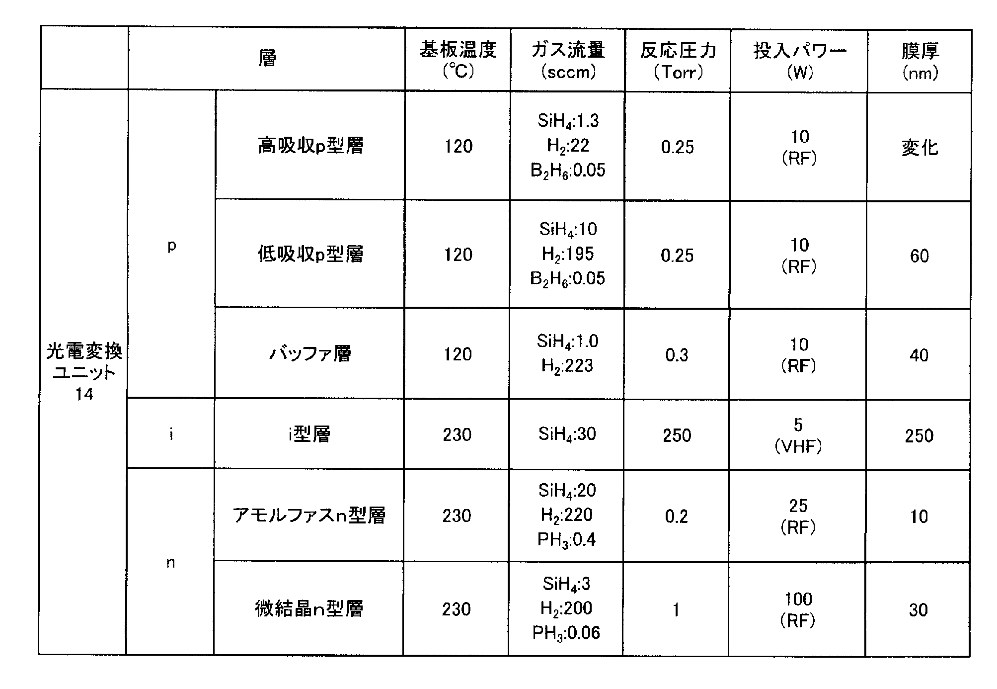
- each layer was formed under the film forming conditions shown in Table 1.
- the configuration of the photoelectric conversion unit 14 is not limited to this.
- the back electrode 16 functions as an electrode for taking out the carrier generated in the photoelectric conversion unit 14 to the outside of the photoelectric conversion device 100 and as a reflection film for reflecting the light transmitted through the photoelectric conversion unit 14 to the photoelectric conversion unit 14. Fulfills the function.
- the back electrode 16 preferably has a laminated structure of a reflective metal and a transparent conductive oxide (TCO).
- TCO transparent conductive oxide
- As the reflective metal metals such as silver (Ag) and aluminum (Al) can be used.
- TCO transparent conductive oxides (TCO) such as tin oxide (SnO 2 ), zinc oxide (ZnO), and indium tin oxide (ITO) are used.
- TCO can be formed by, for example, sputtering.
- the back electrode 16 preferably has a thickness of about 1 ⁇ m in total. It is preferable to provide unevenness on at least one of the back electrodes 16 for enhancing the light confinement effect.
- the filler 18 and the protective film 20 can be made of a resin material such as EVA or polyimide. This can prevent moisture from entering the photoelectric conversion device 100.
- the transparent conductive film 12, the photoelectric conversion unit 14, and the back electrode 16 may be separated by a laser to connect a plurality of cells in series.
- a laser a YAG laser (fundamental wave 1064 nm, second harmonic 532 nm) can be used.
- the p-type layer 14p including the high-absorption p-type layer 14a and the low-absorption p-type layer 14b is formed in the Dt direction (the normal direction of the light-receiving surface of the substrate 10 or the transparent conductive film 12 on the substrate 10, As the unevenness of the texture structure becomes steeper (as the inclination angle ⁇ n of the unevenness increases) with respect to the film thickness of the photoelectric conversion unit 14 and the back electrode 16, the De direction of the transparent conductive film 12 (transparent conductive) The film thickness of the p-type layer 14p (the high absorption p-type layer 14a and the low absorption p-type layer 14b) in the surface normal direction of the film 12 becomes thinner.
- the inclination angle ⁇ n is an acute angle defined by the normal line of the light-receiving surface of the substrate 10 and the normal line of the concavo-convex surface of the transparent conductive layer 12, and its value has a range of 0 ° to 90 °.
- the De direction of the transparent conductive film 12 coincides with the internal electric field direction in the photoelectric conversion device 100, and the open-circuit voltage of the photoelectric conversion device 100 decreases as the thickness of the p-type layer 14p in the De direction decreases. It is considered a thing. Even in the plane of the transparent conductive film 12, the inclination angle ⁇ n of the unevenness of the texture structure varies, and it is estimated that a particularly steep portion causes a decrease in the open circuit voltage.
- FIG. 3 shows the measurement result of the inclination angle ⁇ n of the unevenness of the texture structure of the transparent conductive film 12 using an atomic force microscope (AFM).
- the horizontal axis indicates the inclination angle ⁇ n of the unevenness of the texture structure of the transparent conductive film 12
- the vertical axis indicates the number of measurement points having each inclination angle ⁇ n.
- the measurement was performed as follows. As shown in FIG. 4, the height at each coordinate of the measurement point n of horizontal: 1024 points ⁇ vertical: 768 points was measured. The measurement range is horizontal: 20 ⁇ m ⁇ vertical: 15 ⁇ m. At this time, the actual height was divided by 20 ⁇ m / 1024, and the angles of the triangular portions a, b, and c shown in FIG. 4 were calculated using Equation (1). In this way, the inclination angle ⁇ n of the unevenness of the texture structure was obtained over the entire measurement surface.
- the maximum angle of the four surrounding surfaces at an arbitrary measurement point excluding the place where the local maximum value is obtained is defined as the inclination angle ⁇ n of the texture structure unevenness of the measurement point.
- the inclination angle ⁇ e of the unevenness of the texture structure at the measurement point e is set to four surrounding surfaces (surfaces formed by bde, be The maximum angle among the angles of the plane formed by -f, the plane formed by dh, and the plane formed by efh was adopted.
- the distribution of the unevenness of the texture structure is observed in the range of 0 to 80 ° with a peak near the inclination angle of 40 °.
- the unevenness distribution of the texture structure was observed in the range of 0 to 70 ° with a peak near the inclination angle of 28 °.
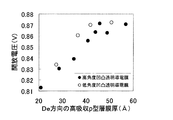
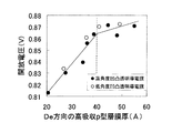
- ⁇ Optimization of p-type layer thickness> 7 to 11 show the relationship of the open circuit voltage with respect to the film thickness of the high absorption p-type layer 14a in the electric field direction (De direction in FIG. 2).
- FIG. 7 shows a case where the average value (arithmetic average value) of the distribution of the inclination angle ⁇ n is used as the angle ⁇ when calculating the film thickness of the high absorption p-type layer 14a in the electric field direction.
- 8 to 11 show the distribution of the number of measurement points having the inclination angle with respect to the inclination angle shown in FIG. 3 when calculating the film thickness of the high absorption p-type layer 14a in the electric field direction.
- an angle ⁇ is used in which the number of measurement points having an inclination angle of up to 97%, 98%, 99%, and 99.5% of the total number of measurement points.
- the angle ⁇ at 99% corresponds to the steepest inclination angle among 99% of the total number of measurement points.
- the film thickness of the high-absorption p-type layer 14a in the electric field direction is calculated using the angle ⁇ at 99%, the open voltages of the high-angle uneven transparent conductive film and the low-angle uneven transparent conductive film best match. (FIG. 10). Therefore, by using this angle ⁇ , the relationship between the film thickness of the high absorption p-type layer 14a in the electric field direction and the open circuit voltage is analyzed to obtain the optimum film thickness of the p-type layer 14p.
- the film thickness of the high absorption p-type layer 14a in the electric field direction is preferably 5 nm, that is, the film thickness of the high absorption p-type layer 14a is preferably 5 / cos ⁇ (nm) or less.
- the angle ⁇ at 99% (the angle ⁇ at which the number of measurement points having an inclination angle from 0 ° to angle ⁇ is integrated and the value becomes 99% or less of the total number of measurement points) is high.
- the film thickness of the absorption p-type layer 14a is preferably 4 / cos ⁇ (nm) or more and 5 / cos ⁇ (nm) or less.
- the film thickness of the p-type layer 14p is [4 / cos ⁇ (nm). It is preferable that the value is + the film thickness of the low absorption p-type layer 14b] or more and [5 / cos ⁇ (nm) + the film thickness of the low absorption p-type layer 14b] or less.
- the inclination angle ⁇ n is dispersed in the vicinity of the smallest possible angle. Specifically, it is preferable that the angle ⁇ at which 99% of the inclination angle ⁇ n of the unevenness of the texture structure is equal to or less than that value is 60 ° or less.
Landscapes
- Photovoltaic Devices (AREA)
Abstract
基板上に、表面に凹凸を有する透明導電膜を形成する第1の工程と、基板の受光面の法線と透明導電膜の凹凸表面の法線とで規定される鋭角である透明導電膜の凹凸の傾斜角度θnを、複数の測定点で算出する第2の工程と、透明導電膜上に高吸収p型層と、高吸収p型層上に低吸収p型層とを形成する第3の工程と、を備え、第3の工程では、高吸収p型層の膜厚を、傾斜角度θnの分布において0°から角度θまでの測定点の数が測定点の総数の99%となる角度θに対して、4/cosθ(nm)以上5/cosθ(nm)以下となるように形成する。
Description
本発明は、光電変換装置の製造方法に関する。
多結晶、微結晶またはアモルファスシリコンを用いた薄膜型の光電変換装置が知られている。このような薄膜型光電変換装置は、資源消費の観点、コストの低下の観点および効率化の観点から注目されている。
光電変換装置では、基板上に形成された透明導電膜にテクスチャ構造を形成し、その透明導電膜上に半導体からなる光電変換層を積層した構成が採用されている。このようにテクスチャ構造を採ることによって、光電変換層へ入射される光の光路長を伸ばす光閉じ込め効果が得られる(特許文献1参照)。
ところで、テクスチャ構造の凹凸の角度を急峻にすることで光閉じ込め効果が向上し、光電変換装置の短絡電流を増加させることができる。しかしながら、同時に光電変換装置の開放電圧が低下するという問題があった。
本発明の1つの態様は、基板上に、表面に凹凸を有する透明導電膜を形成する第1の工程と、基板の受光面の法線と透明導電膜の凹凸表面の法線とで規定される鋭角である透明導電膜の凹凸の傾斜角度θn、を複数の測定点で算出する第2の工程と、透明導電膜上にp型のドーパントを含む第1のp型層と、第1のp型層上に第1のp型層よりp型のドーパントの濃度が低い第2のp型層とを形成する第3の工程と、を備え、第3の工程では、第1のp型層の膜厚を、傾斜角度θnの分布において0°から角度θまでの測定点の数が測定点の総数の99%となる角度θに対して、4/cosθ(nm)以上5/cosθ(nm)以下となるように形成する、光電変換装置の製造方法である。
本発明によれば、テクスチャ構造による開放電圧の劣化を生じさせることなく、光閉じ込め効果を高めた光電変換装置の製造方法を提供することができる。
<基本構成>
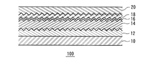
本発明の実施の形態における光電変換装置100は、図1の断面図に示すように、基板10、透明導電膜12、光電変換ユニット14、裏面電極16、充填材18及び保護膜20が積層された構造を有する。
本発明の実施の形態における光電変換装置100は、図1の断面図に示すように、基板10、透明導電膜12、光電変換ユニット14、裏面電極16、充填材18及び保護膜20が積層された構造を有する。
基板10は、光電変換に利用される波長帯の光を透過する材料を用いる。例えば、ガラス基板、プラスチック基板等の少なくとも可視光波長領域において透過性を有する材料を適用することができる。
基板10上に透明導電膜12が形成される。透明導電膜12は、光電変換ユニット14で発生したキャリアを光電変換装置100の外部へ取り出すための電極として機能すると共に、光電変換ユニット14へ外部からの光を透過する機能を果たす。また、透明導電膜12は、光電変換ユニット14へ入射される光に対する反射防止膜としても機能する。透明導電膜12は、酸化錫(SnO2)、酸化亜鉛(ZnO)、インジウム錫酸化物(ITO)等に錫(Sn)、アンチモン(Sb)、フッ素(F)、アルミニウム(Al)等をドープした透明導電性酸化物(TCO)のうち少なくとも一種類又は複数種を組み合わせて用いることが好適である。特に、酸化亜鉛(ZnO)は、透光性が高く、抵抗率が低く、耐プラズマ特性にも優れているので好適である。透明導電膜12は、例えば、スパッタリング等により形成することができる。透明導電膜12の膜厚は0.5μm以上5μm以下の範囲とすることが好適である。
スパッタリングにより形成した透明導電膜12をエッチングすることによって、透明導電膜12の表面には光閉じ込め効果を奏するためのテクスチャ構造となる凹凸を設ける。テクスチャ構造の凹凸の角度、凹凸の大きさ等は、エッチングの条件(エッチング液の種類、濃度、時間等)を調整することによって変化させることができる。また、本実施の形態でのテクスチャ構造の凹凸は、後述する傾斜角度θnに関して、平均的な角度が30°以上となるように調整している。なお、上記方法に代えて、MOCVD法で透明導電膜を形成することでも、表面に凹凸を有する透明導電膜12を形成できる。この場合は、MOCVD法の成膜条件(圧力、温度、時間、流量等)を調整することによってテクスチャ構造の形状を変化させることができる。
透明導電膜12上には光電変換ユニット14が形成される。光電変換ユニット14は、p型層とn型層とを積層したpn接合、又はp型層、i型層、n型層を積層したpin接合を有する半導体膜の積層体である。光電変換ユニット14は、アモルファスシリコン薄膜や微結晶シリコン薄膜を積層したアモルファスシリコン(a-Si)光電変換ユニットや微結晶シリコン(μc-Si)光電変換ユニット、又はそれらを積層したタンデム型光電変換ユニットとすることができる。
本実施の形態では、透明導電膜12上にp型層として高吸収p型層、低吸収p型層及びバッファ層を形成し、p型層上にi型層を形成し、i型層上にアモルファスn型層及び微結晶n型層を積層した光電変換ユニットを形成した。高吸収p型層とは、p型のドーパントの濃度が低吸収p型層に比べて高く、光の吸収率が低吸収p型層に比べて大きいp型層をいう。低吸収p型層とは、p型のドーパントの濃度が高吸収p型層に比べて低く、光の吸収率が高吸収p型層に比べて小さいp型層をいう。具体的には、表1に示す成膜条件にて各層を形成した。ただし、光電変換ユニット14の構成はこれに限定されるものではない。
裏面電極16は、光電変換ユニット14で発生したキャリアを光電変換装置100の外部へ取り出すための電極として機能すると共に、光電変換ユニット14を透過してきた光を光電変換ユニット14へ反射させる反射膜としての機能を果たす。裏面電極16は、反射性金属と透明導電性酸化物(TCO)との積層構造とすることが好ましい。反射性金属としては、銀(Ag)、アルミニウム(Al)等の金属が使用できる。また、TCOとしては、酸化錫(SnO2)、酸化亜鉛(ZnO)、インジウム錫酸化物(ITO)等の透明導電性酸化物(TCO)が用いられる。TCOは、例えば、スパッタリング等により形成することができる。裏面電極16は、合わせて1μm程度の膜厚とすることが好適である。裏面電極16の少なくとも一方には、光閉じ込め効果を高めるための凹凸を設けることが好適である。
さらに、充填材18を介して保護膜20で裏面電極16の表面を被う。充填材18及び保護膜20は、EVA、ポリイミド等の樹脂材料とすることができる。これによって、光電変換装置100への水分の侵入等を防ぐことができる。
また、レーザによって透明導電膜12、光電変換ユニット14、裏面電極16の分離加工を行うことによって、複数のセルを直列に接続した構成にしてもよい。レーザには、YAGレーザ(基本波1064nm、2倍高調波532nm)を用いることができる。
<透明導電膜のテクスチャ構造の評価>
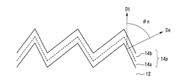
図2に示すように、高吸収p型層14a及び低吸収p型層14bを含むp型層14pはDt方向(基板10の受光面の法線方向もしくは基板10上への透明導電膜12、光電変換ユニット14、裏面電極16の積層方向に相当)の膜厚に対して、テクスチャ構造の凹凸が急峻になるほど(凹凸の傾斜角度θnが大きくなるほど)、透明導電膜12のDe方向(透明導電膜12の表面法線方向)のp型層14p(高吸収p型層14a及び低吸収p型層14b)の膜厚がより薄くなる。ここで、傾斜角度θnは、基板10の受光面の法線と、透明導電層12の凹凸表面の法線とで規定される鋭角であり、その値は0°から90°の範囲を有する。透明導電膜12のDe方向は、光電変換装置100における内部電界方向と一致し、このDe方向に向けてのp型層14pの膜厚が薄くなることにより光電変換装置100の開放電圧が低下するものと考えられる。透明導電膜12の面内でもテクスチャ構造の凹凸の傾斜角度θnにはばらつきがあり、特に急峻な部分が開放電圧の低下を招いていると推考される。
図2に示すように、高吸収p型層14a及び低吸収p型層14bを含むp型層14pはDt方向(基板10の受光面の法線方向もしくは基板10上への透明導電膜12、光電変換ユニット14、裏面電極16の積層方向に相当)の膜厚に対して、テクスチャ構造の凹凸が急峻になるほど(凹凸の傾斜角度θnが大きくなるほど)、透明導電膜12のDe方向(透明導電膜12の表面法線方向)のp型層14p(高吸収p型層14a及び低吸収p型層14b)の膜厚がより薄くなる。ここで、傾斜角度θnは、基板10の受光面の法線と、透明導電層12の凹凸表面の法線とで規定される鋭角であり、その値は0°から90°の範囲を有する。透明導電膜12のDe方向は、光電変換装置100における内部電界方向と一致し、このDe方向に向けてのp型層14pの膜厚が薄くなることにより光電変換装置100の開放電圧が低下するものと考えられる。透明導電膜12の面内でもテクスチャ構造の凹凸の傾斜角度θnにはばらつきがあり、特に急峻な部分が開放電圧の低下を招いていると推考される。
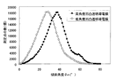
図3は、原子間力顕微鏡(AFM)を用いて透明導電膜12のテクスチャ構造の凹凸の傾斜角度θnを測定した結果を示す。図3では、横軸が透明導電膜12のテクスチャ構造の凹凸の傾斜角度θn、縦軸が各傾斜角度θnを有する測定点の数を示す。
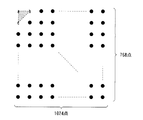
測定は、以下のように行った。図4に示すように、横:1024点×縦:768点の測定点nの各座標における高さを測定した。測定範囲は、横:20μm×縦:15μmである。このとき、実際の高さを20μm/1024で割った値とし、図4に示したa,b,cの三角形の部分の角度は数式(1)を用いて算出した。このようにして、測定面の全域に亘ってテクスチャ構造の凹凸の傾斜角度θnを求めた。

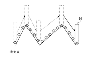
このとき、図5に示すように、AFMの探針30の太さと解像度により、測定点によって定義される面がテクスチャ構造の凹凸の稜線を跨ぐ場合には、頂上部の形状を反映せずに探針30が水平に移動したものと見なされ、実際の傾斜角度より測定される傾斜角度が小さくなる。したがって、これらの測定点のデータは除外することが望ましい。
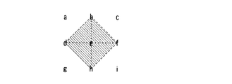
今回は、極大値となる箇所を除いた任意の測定点において、その周囲の4つの面のうち最大の角度をその測定点のテクスチャ構造の凹凸の傾斜角度θnとした。例えば、図6に示す9箇所の測定点a~iにおいて、測定点eでのテクスチャ構造の凹凸の傾斜角度θeは周囲の4つの面(b-d-eで形成される面、b-e-fで形成される面、d-e-hで形成される面、e-f-hで形成される面)の角度のうち最大の角度を採用した。
このような測定によって、図3に示すように、高角度凹凸透明導電膜では傾斜角度40°付近をピークとして0~80°の範囲においてテクスチャ構造の凹凸の角度の分布がみられ、低角度凹凸透明導電膜では傾斜角度28°付近をピークとして0~70°の範囲においてテクスチャ構造の凹凸の角度の分布がみられた。
<p型層の膜厚の最適化>
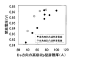
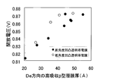
図7~図11は、電界方向(図2のDe方向)の高吸収p型層14aの膜厚に対する開放電圧の関係を示す。図7は、電界方向の高吸収p型層14aの膜厚を算出する際に角度θとして傾斜角度θnの分布の平均値(算術平均値)を用いた場合を示す。図8~図11は、電界方向の高吸収p型層14aの膜厚を算出する際に、図3に示した傾斜角度に対する当該傾斜角度を有する測定点の数の分布において0°から角度θまでの傾斜角度を有する測定点の数が測定点の総数の97%、98%、99%及び99.5%となる角度θを用いた場合を示す。以下、それぞれを、97%での角度θ、98%での角度θ、99%での角度θ、99.5%での角度θと記す。なお、例えば、99%での角度θは、測定点の総数の99%の中で最も急峻な傾斜角度に相当する。
図7~図11は、電界方向(図2のDe方向)の高吸収p型層14aの膜厚に対する開放電圧の関係を示す。図7は、電界方向の高吸収p型層14aの膜厚を算出する際に角度θとして傾斜角度θnの分布の平均値(算術平均値)を用いた場合を示す。図8~図11は、電界方向の高吸収p型層14aの膜厚を算出する際に、図3に示した傾斜角度に対する当該傾斜角度を有する測定点の数の分布において0°から角度θまでの傾斜角度を有する測定点の数が測定点の総数の97%、98%、99%及び99.5%となる角度θを用いた場合を示す。以下、それぞれを、97%での角度θ、98%での角度θ、99%での角度θ、99.5%での角度θと記す。なお、例えば、99%での角度θは、測定点の総数の99%の中で最も急峻な傾斜角度に相当する。
ここで、99%での角度θを用いて電界方向の高吸収p型層14aの膜厚を算出したときに高角度凹凸透明導電膜及び低角度凹凸透明導電膜の開放電圧が最もよく一致する(図10)。そこで、この角度θを用いて電界方向の高吸収p型層14aの膜厚と開放電圧との関係を解析して最適なp型層14pの膜厚を求める。
図10の実線で示すように、電界方向の高吸収p型層14aの膜厚が4nm(=40Å)までは膜厚が減少すると共に開放電圧が緩やかに減少し、4nmより小さくなると開放電圧の減少は急激になる。そうすると、電界方向の高吸収p型層14aの膜厚は4nm以上とすることが好ましい。すなわち、高吸収p型層14aを形成する工程での成膜膜厚は、テクスチャ構造の凹凸の傾斜角度θnの分布に関係なく、99%での角度θに対して4/cosθ(nm)以上とすることが好適である。
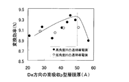
図12及び図13は、電界方向の高吸収p型層14aの膜厚に対する短絡電流密度及び変換効率との関係を示す。ここでの電界方向の高吸収p型層14aの膜厚は、99%での角度θを用いて算出した。
図12及び図13の実線に示されるように、電界方向の高吸収p型層14aの膜厚が5nm(=50Å)より大きくなると短絡電流密度及び変換効率が急激に低下する。したがって、電界方向の高吸収p型層14aの膜厚は5nm、すなわち高吸収p型層14aの膜厚は5/cosθ(nm)以下とすることが好適である。
以上より、99%での角度θ(0°から角度θまでの傾斜角度を有する測定点の数を積算してその値が測定点の総数の99%以下となる角度θ)に対して、高吸収p型層14aの膜厚は、4/cosθ(nm)以上5/cosθ(nm)以下とすることが好適である。これにより、テクスチャ構造による開放電圧の劣化を生じさせることなく、光閉じ込め効果を高めた光電変換装置を効率よく製造することができる。
また、p型層14pの全膜厚は、高吸収p型層14a及び低吸収p型層14bの膜厚の合計であるので、p型層14pの膜厚は、[4/cosθ(nm)+低吸収p型層14bの膜厚]以上[5/cosθ(nm)+低吸収p型層14bの膜厚]以下とすることが好適である。
また、傾斜角度θnの大きい凹凸が開放電圧の低下を招いていると推考されるので、傾斜角度θnはできるだけ小さい角度の付近に分散するようにすることが好適である。具体的には、テクスチャ構造の凹凸の傾斜角度θnのうち99%がその値以下となる角度θが60°以下となるようにすることが好適である。
Claims (3)
- 基板上に、表面に凹凸を有する透明導電膜を形成する第1の工程と、
前記基板の受光面の法線と前記透明導電膜の凹凸表面の法線とで規定される鋭角である前記透明導電膜の凹凸の傾斜角度θnを、複数の測定点で算出する第2の工程と、
前記透明導電膜上にp型のドーパントを含む第1のp型層と、前記第1のp型層上に前記第1のp型層よりp型のドーパントの濃度が低い第2のp型層とを形成する第3の工程と、
を備え、
前記第3の工程では、前記第1のp型層の膜厚を、前記傾斜角度θnの分布において0°から角度θまでの測定点の数が測定点の総数の99%となる角度θに対して、4/cosθ(nm)以上5/cosθ(nm)以下となるように形成することを特徴とする光電変換装置の製造方法。 - 請求項1に記載の光電変換装置の製造方法であって、
前記第1の工程では、前記透明導電膜の凹凸を、前記傾斜角度θnの分布の平均値が30°以上となるように形成することを特徴とする光電変換装置の製造方法。 - 請求項1に記載の光電変換装置の製造方法であって、
前記第2の工程では、原子間力顕微鏡(AFM)を用いて前記透明導電膜の凹凸状態を測定し、その結果を用いて前記透明導電膜の凹凸の前記傾斜角度θnを算出することを特徴とする光電変換装置の製造方法。
Applications Claiming Priority (2)
| Application Number | Priority Date | Filing Date | Title |
|---|---|---|---|
| JP2011-066505 | 2011-03-24 | ||
| JP2011066505 | 2011-03-24 |
Publications (1)
| Publication Number | Publication Date |
|---|---|
| WO2012127970A1 true WO2012127970A1 (ja) | 2012-09-27 |
Family
ID=46879132
Family Applications (1)
| Application Number | Title | Priority Date | Filing Date |
|---|---|---|---|
| PCT/JP2012/054269 Ceased WO2012127970A1 (ja) | 2011-03-24 | 2012-02-22 | 光電変換装置の製造方法 |
Country Status (1)
| Country | Link |
|---|---|
| WO (1) | WO2012127970A1 (ja) |
Citations (2)
| Publication number | Priority date | Publication date | Assignee | Title |
|---|---|---|---|---|
| JPH09260704A (ja) * | 1996-03-27 | 1997-10-03 | Sharp Corp | 太陽電池の製造方法 |
| JP2011014618A (ja) * | 2009-06-30 | 2011-01-20 | Sanyo Electric Co Ltd | 太陽電池及びその製造方法 |
-
2012
- 2012-02-22 WO PCT/JP2012/054269 patent/WO2012127970A1/ja not_active Ceased
Patent Citations (2)
| Publication number | Priority date | Publication date | Assignee | Title |
|---|---|---|---|---|
| JPH09260704A (ja) * | 1996-03-27 | 1997-10-03 | Sharp Corp | 太陽電池の製造方法 |
| JP2011014618A (ja) * | 2009-06-30 | 2011-01-20 | Sanyo Electric Co Ltd | 太陽電池及びその製造方法 |
Similar Documents
| Publication | Publication Date | Title |
|---|---|---|
| JP5150473B2 (ja) | 積層型光電変換装置 | |
| JP4222500B2 (ja) | シリコン系薄膜光電変換装置 | |
| KR101319750B1 (ko) | 반도체 다층 스택을 구비한 광전지 모듈 및 광전지 모듈의 제작 방법 | |
| CN103999242B (zh) | 晶体硅太阳能电池、太阳能电池模块及其制造方法 | |
| US8710357B2 (en) | Transparent conductive structure | |
| CN102473748A (zh) | 薄膜太阳能电池及其制造方法 | |
| CN103238218B (zh) | 多结光电器件及其生产工艺 | |
| CN102934234A (zh) | 使用增强的光捕获方案的薄膜光伏器件 | |
| US20130199608A1 (en) | Method for manufacturing a photovoltaic cell comprising a tco layer | |
| JPWO2017217219A1 (ja) | 太陽電池及びその製造方法、並びに太陽電池モジュール | |
| WO2012105155A1 (ja) | 光電変換装置及びその製造方法 | |
| EP2561548A1 (en) | Improved method for manufacturing a photovoltaic cell comprising a tco layer | |
| JP2010141192A (ja) | 薄膜太陽電池セルおよび薄膜太陽電池 | |
| JP2016086154A (ja) | 太陽電池モジュール | |
| JP3203106B2 (ja) | 光起電力装置 | |
| WO2011136177A1 (ja) | 薄膜太陽電池およびその製造方法、透明導電膜付き基体およびその製造方法 | |
| KR101086260B1 (ko) | 플렉서블 기판 또는 인플렉서블 기판을 포함하는 광기전력 장치 및 광기전력 장치의 제조 방법 | |
| EP2738819B1 (en) | Solar cell | |
| JP5036663B2 (ja) | 薄膜太陽電池およびその製造方法 | |
| JP5542038B2 (ja) | 薄膜太陽電池およびその製造方法、薄膜太陽電池モジュール | |
| Ahrlich et al. | Improved light management in silicon heterojunction solar cells by application of a ZnO nanorod antireflective layer | |
| US20190341516A1 (en) | MICROSTRUCTURED ZnO COATINGS FOR IMPROVED PERFORMANCE IN Cu(In, Ga)Se2 PHOTOVOLTAIC DEVICES | |
| TW201414001A (zh) | 用於太陽能電池之經特意摻雜的氧化鎘層 | |
| JP2014063819A (ja) | 光電変換装置および光電変換装置の製造方法 | |
| KR20120064268A (ko) | 박막 태양전지 및 이의 제조 방법 |
Legal Events
| Date | Code | Title | Description |
|---|---|---|---|
| 121 | Ep: the epo has been informed by wipo that ep was designated in this application |
Ref document number: 12761066 Country of ref document: EP Kind code of ref document: A1 |
|
| NENP | Non-entry into the national phase |
Ref country code: DE |
|
| 122 | Ep: pct application non-entry in european phase |
Ref document number: 12761066 Country of ref document: EP Kind code of ref document: A1 |
|
| NENP | Non-entry into the national phase |
Ref country code: JP |