WO2012121282A1 - 紫外線センサ、及び紫外線センサの製造方法 - Google Patents
紫外線センサ、及び紫外線センサの製造方法 Download PDFInfo
- Publication number
- WO2012121282A1 WO2012121282A1 PCT/JP2012/055801 JP2012055801W WO2012121282A1 WO 2012121282 A1 WO2012121282 A1 WO 2012121282A1 JP 2012055801 W JP2012055801 W JP 2012055801W WO 2012121282 A1 WO2012121282 A1 WO 2012121282A1
- Authority
- WO
- WIPO (PCT)
- Prior art keywords
- type semiconductor
- semiconductor layer
- internal electrode
- ultraviolet sensor
- high resistance
- Prior art date
- Legal status (The legal status is an assumption and is not a legal conclusion. Google has not performed a legal analysis and makes no representation as to the accuracy of the status listed.)
- Ceased
Links
Images




Classifications
-
- H—ELECTRICITY
- H10—SEMICONDUCTOR DEVICES; ELECTRIC SOLID-STATE DEVICES NOT OTHERWISE PROVIDED FOR
- H10F—INORGANIC SEMICONDUCTOR DEVICES SENSITIVE TO INFRARED RADIATION, LIGHT, ELECTROMAGNETIC RADIATION OF SHORTER WAVELENGTH OR CORPUSCULAR RADIATION
- H10F77/00—Constructional details of devices covered by this subclass
- H10F77/40—Optical elements or arrangements
- H10F77/407—Optical elements or arrangements indirectly associated with the devices
-
- G—PHYSICS
- G01—MEASURING; TESTING
- G01J—MEASUREMENT OF INTENSITY, VELOCITY, SPECTRAL CONTENT, POLARISATION, PHASE OR PULSE CHARACTERISTICS OF INFRARED, VISIBLE OR ULTRAVIOLET LIGHT; COLORIMETRY; RADIATION PYROMETRY
- G01J1/00—Photometry, e.g. photographic exposure meter
- G01J1/02—Details
- G01J1/0252—Constructional arrangements for compensating for fluctuations caused by, e.g. temperature, or using cooling or temperature stabilization of parts of the device; Controlling the atmosphere inside a photometer; Purge systems, cleaning devices
-
- G—PHYSICS
- G01—MEASURING; TESTING
- G01J—MEASUREMENT OF INTENSITY, VELOCITY, SPECTRAL CONTENT, POLARISATION, PHASE OR PULSE CHARACTERISTICS OF INFRARED, VISIBLE OR ULTRAVIOLET LIGHT; COLORIMETRY; RADIATION PYROMETRY
- G01J1/00—Photometry, e.g. photographic exposure meter
- G01J1/42—Photometry, e.g. photographic exposure meter using electric radiation detectors
- G01J1/429—Photometry, e.g. photographic exposure meter using electric radiation detectors applied to measurement of ultraviolet light
-
- H—ELECTRICITY
- H10—SEMICONDUCTOR DEVICES; ELECTRIC SOLID-STATE DEVICES NOT OTHERWISE PROVIDED FOR
- H10F—INORGANIC SEMICONDUCTOR DEVICES SENSITIVE TO INFRARED RADIATION, LIGHT, ELECTROMAGNETIC RADIATION OF SHORTER WAVELENGTH OR CORPUSCULAR RADIATION
- H10F71/00—Manufacture or treatment of devices covered by this subclass
-
- H—ELECTRICITY
- H10—SEMICONDUCTOR DEVICES; ELECTRIC SOLID-STATE DEVICES NOT OTHERWISE PROVIDED FOR
- H10F—INORGANIC SEMICONDUCTOR DEVICES SENSITIVE TO INFRARED RADIATION, LIGHT, ELECTROMAGNETIC RADIATION OF SHORTER WAVELENGTH OR CORPUSCULAR RADIATION
- H10F77/00—Constructional details of devices covered by this subclass
- H10F77/10—Semiconductor bodies
- H10F77/12—Active materials
- H10F77/123—Active materials comprising only Group II-VI materials, e.g. CdS, ZnS or HgCdTe
-
- H—ELECTRICITY
- H10—SEMICONDUCTOR DEVICES; ELECTRIC SOLID-STATE DEVICES NOT OTHERWISE PROVIDED FOR
- H10F—INORGANIC SEMICONDUCTOR DEVICES SENSITIVE TO INFRARED RADIATION, LIGHT, ELECTROMAGNETIC RADIATION OF SHORTER WAVELENGTH OR CORPUSCULAR RADIATION
- H10F77/00—Constructional details of devices covered by this subclass
- H10F77/20—Electrodes
- H10F77/206—Electrodes for devices having potential barriers
Definitions
- the present invention relates to an ultraviolet sensor and a method for manufacturing the ultraviolet sensor. More specifically, the present invention relates to a photodiode-type ultraviolet ray having a laminated structure in which a p-type semiconductor layer and an n-type semiconductor layer are heterojunction using an oxide compound semiconductor. The present invention relates to a sensor and a manufacturing method thereof.
- UV sensors are widely used as ultraviolet light detection devices such as germicidal lamps for sterilizing bacteria floating in the air or water, and ultraviolet irradiation devices, and in recent years, they are also expected to be applied to optical communication devices.
- this type of ultraviolet sensor uses a diamond semiconductor or SiC semiconductor as a sensor material.
- these diamond semiconductors and SiC semiconductors have the disadvantage that they are inferior in material processability and are expensive.
- oxide compound semiconductors that are easy to process materials and are relatively inexpensive.
- An ultraviolet sensor in which a p-type semiconductor layer and an n-type semiconductor layer are heterojunction using these oxide compound semiconductors. Research and development are actively conducted.
- Patent Document 1 As shown in FIG. 11, one of a (Ni, Zn) O layer 101 made of an oxide compound semiconductor formed by dissolving ZnO in NiO and the (Ni, Zn) O layer 101.
- a thin film material layer 103 formed by a sputtering method so as to cover a part of the main surface 102, and first and second terminal electrodes 104a and 104b formed at both ends of the (Ni, Zn) O layer 101;
- An internal electrode 105 is formed in the (Ni, Zn) O layer 101, the first terminal electrode 104a is electrically connected to the internal electrode 105, and the second terminal electrode 104b Has proposed an ultraviolet sensor electrically connected to the thin film material layer 103.
- one end of the internal electrode 105 is electrically connected to the terminal electrode 104 a and the other end is formed to extend to a substantially central portion in the (Ni, Zn) O layer 101. Further, the thin film material layer 103 is arranged to face the internal electrode 105 and is formed so as to partially overlap the internal electrode 105 in a plan view. Further, the thin film material layer 103 is formed on the other terminal electrode 104b. It is connected.
- JP 2010-87482 A (Claim 1, FIG. 1)
- Patent Document 1 As described above, a photovoltaic force is generated according to the ultraviolet intensity at the overlapping portion a between the thin film material layer 103 and the internal electrode 105. Therefore, in order to ensure the reliability of detection accuracy, It is necessary to obtain stable photosensitivity without variation between products.
- the overlapping portion a is likely to vary in both the longitudinal direction and the width direction of the internal electrode 105. Moreover, since the thin film material layer 103 is formed by a sputtering method, the dimensions of the thin film material layer 103 are likely to vary. Accordingly, the area of the overlapping portion a between the internal electrode 105 and the thin film material layer 103 (hereinafter referred to as “overlapping area”) is likely to vary between products, and therefore the response intensity to ultraviolet light also varies between products. It is difficult to obtain a photovoltaic power which is easy and has high accuracy and reliability.
- a diode is formed between the (Ni, Zn) O layer 101 and the thin film material layer 103 by a pn junction.
- a resistor is formed between the second terminal electrode 104b and a closed circuit is formed. For this reason, a weak current generated when ultraviolet rays are not irradiated flows through the closed circuit and leaks from the internal electrode 105 to the terminal electrode 104b, which may increase the dark current.
- the present invention has been made in view of such circumstances, and is capable of suppressing variation in characteristics between products, and has a high sensitivity and high output ultraviolet sensor with low dark current and good reliability, and a method for manufacturing the same.
- the purpose is to provide.
- an ultraviolet sensor includes a p-type semiconductor layer mainly composed of a solid solution of NiO and ZnO, and an n-type semiconductor mainly composed of ZnO bonded to the p-type semiconductor layer.
- the n-type semiconductor layer has a part of the p-type semiconductor layer exposed on the surface
- the both ends of the internal electrode are exposed to both end faces of the p-type semiconductor layer, and the high resistance layer made of an insulating material is connected to one end of the internal electrode.
- the first external electrode is electrically connected to the other end of the internal electrode, and the second external electrode is electrically connected to the n-type semiconductor layer. It is characterized by being.
- the internal electrode is formed from one end face of the p-type semiconductor layer to the other end face. Therefore, it is possible to suppress dimensional variation in the longitudinal direction of the internal electrode between products, and it is possible to reduce the occurrence of variation in the overlapping area formed between the opposing n-type semiconductor layers.
- the high-resistance layer includes a first high-resistance layer made of the insulating material interposed between the second external electrode and the p-type semiconductor layer, and the internal It is preferable that the insulating material has a second high resistance layer diffused in the p-type semiconductor layer so as to cover the one end portion of the electrode.
- the width dimension of the n-type semiconductor layer along the end face direction of the p-type semiconductor layer is wider than the width dimension of the internal electrode arranged to face the n-type semiconductor layer. It is preferable that it is formed.
- the width dimension of the internal electrode is smaller than the width dimension of the n-type semiconductor layer, it is possible for the n-type semiconductor layer to absorb the dimension variation in the width direction of the internal electrode between products. Therefore, the overlapping area can be stabilized as a whole between products, and the response variation between products with respect to the ultraviolet intensity can be effectively suppressed.
- the width dimension of the internal electrode along the end face direction of the p-type semiconductor layer is formed wider than the width dimension of the n-type semiconductor layer arranged to face the internal electrode. It is also preferable.
- the width dimension of the n-type semiconductor layer is smaller than the width dimension of the internal electrode, even if a dimensional variation occurs in the n-type semiconductor layer, it does not protrude from the internal electrode, and the overlapping area can be increased. it can. Therefore, it is possible to obtain an ultraviolet sensor having a better response intensity as well as stabilizing the photovoltaic power against ultraviolet irradiation.
- the high resistance layer is colored with a color that can be distinguished from other components.
- the internal electrode is formed of a complex oxide containing rare earth elements and Ni as main components.
- the ultraviolet sensor according to the present invention includes a p-type semiconductor layer mainly composed of a solid solution of NiO and ZnO, an n-type semiconductor layer mainly composed of ZnO bonded to the p-type semiconductor layer, and the n-type semiconductor layer.
- the internal electrode is exposed on both end faces and both side faces of the p-type semiconductor layer, and an insulating material
- a high resistance layer is formed so as to cover both ends of the internal electrode, first and second external electrodes are formed on the surface of the high resistance layer, and the n-type semiconductor layer is The first and second external electrodes are electrically connected, and the third external electrode is formed on the side surface of the p-type semiconductor layer.
- the high resistance layer includes a first high resistance made of the insulating material interposed between the first and second external electrodes and the p-type semiconductor layer. It is preferable to have a layer and a second high resistance layer in which the insulating material is diffused in the p-type semiconductor layer so as to cover the both end portions of the internal electrode.
- the internal electrode is formed of a complex oxide containing a rare earth element and Ni as main components.
- the method for manufacturing an ultraviolet sensor according to the present invention includes a green sheet manufacturing process for manufacturing a plurality of green sheets mainly composed of a solid solution of NiO and ZnO, and a conductive film forming process for forming a conductive film to be an internal electrode.
- the conductive film forming step includes applying a first conductive paste between both end faces of one green sheet among the plurality of green sheets.
- a conductive film is formed, and an insulating paste made of an insulating material is applied to one end portion of the p-type semiconductor layer and baked to diffuse the insulating material into the p-type semiconductor layer. And a high resistance layer forming step of forming a high resistance layer so as to cover one end of the internal electrode.
- the insulating material can be easily diffused in the p-type semiconductor layer including the end portion of the internal electrode to cover one end portion of the internal electrode, and one end portion of the internal electrode can be easily insulated. can do.
- the second conductive paste is applied to the other end of the p-type semiconductor layer and the outer surface of the high resistance layer, and a firing process is performed.
- a color former is added to the insulating material in the high resistance layer forming step.
- the method for manufacturing an ultraviolet sensor according to the present invention includes a green sheet manufacturing process for manufacturing a plurality of green sheets mainly composed of a solid solution of NiO and ZnO, and a conductive film forming process for forming a conductive film to be an internal electrode.
- the conductive powder is formed after slurrying the conductive powder to produce a conductive sheet which is a sheet-like conductive film,
- An insulating paste made of an insulating material is applied to one end of the p-type semiconductor layer and baked, the insulating material is diffused into the p-type semiconductor layer, and one end of the internal electrode is It is characterized by having a high resistance layer forming step of forming a high resistance layer in a covering form.
- the second conductive paste is applied to the other end of the p-type semiconductor layer and the outer surface of the high resistance layer, and a firing process is performed.
- the high resistance layer forming step adds a color former to the insulating material.
- the method for manufacturing an ultraviolet sensor according to the present invention includes a green sheet manufacturing process for manufacturing a plurality of green sheets mainly composed of a solid solution of NiO and ZnO, and a conductive film forming process for forming a conductive film to be an internal electrode.
- the conductive powder is formed after slurrying the conductive powder to produce a conductive sheet which is a sheet-like conductive film,
- a mode in which an insulating paste made of an insulating material is applied to both ends of the p-type semiconductor layer and baked to diffuse the insulating material into the p-type semiconductor layer and cover both ends of the internal electrode A high-resistance layer forming step of forming a high-resistance layer, a second conductive paste is applied to an outer surface of the high-resistance layer and a side surface of the p-type semiconductor layer, and a baking process is performed.
- an external electrode forming step of forming a third external electrode is performed after slurrying the conductive powder to produce a conductive sheet which is a sheet-like conductive film.
- the firing process in the external electrode forming step and the firing process in the high resistance layer forming step are simultaneously performed, and the external electrodes and the high resistance layer are simultaneously manufactured. preferable.
- the n-type semiconductor layer is bonded to the p-type semiconductor layer in a form in which a part of the p-type semiconductor layer is exposed on the surface, and both ends of the internal electrode are connected to the p-type semiconductor layer.
- a high resistance layer made of an insulating material is formed so as to cover one end of the internal electrode, and the first external electrode is electrically connected to the other end of the internal electrode. Since the second external electrode is electrically connected to the n-type semiconductor layer, the internal electrode is formed from one end face of the p-type semiconductor layer to the other end face.
- the internal electrode is exposed on both end surfaces and both side surfaces of the p-type semiconductor layer, and the high resistance layer made of an insulating material covers both end portions of the internal electrode.
- the first and second external electrodes are formed on the surface of the high resistance layer, and the n-type semiconductor layer is electrically connected to the first and second external electrodes.
- the third external electrode is formed on the side surface of the p-type semiconductor layer, the same effect as described above can be obtained even in the case of a three-terminal ultraviolet sensor, and the characteristics vary among products. Can be obtained.
- the conductive film formation step includes forming a conductive film by applying a first conductive paste between both end faces of one green sheet among the plurality of green sheets.
- an insulating paste made of an insulating material is applied to one end of the p-type semiconductor layer and baked to diffuse the insulating material into the p-type semiconductor layer.
- the conductive powder is slurried and then molded to produce a conductive sheet which is a sheet-like conductive film, and the p-type semiconductor
- An insulating paste made of an insulating material is applied to one end of the layer and baked to diffuse the insulating material into the p-type semiconductor layer and cover one end of the internal electrode
- a high-resistance layer forming step for forming a high-resistance layer in various forms, so there is no need to screen-print on a green sheet to form a conductive film, and a laminate can be obtained only by sheet molding Become. That is, in this case, since the conductive film is formed by the sheet method, it can be formed thicker than the printing method. As a result, the resistance of the internal electrode is reduced, thereby improving the output current and the sensor performance. Will improve.
- the conductive powder in the conductive film forming step, is slurried and then molded to produce a conductive sheet which is a sheet-like conductive film, and the p-type semiconductor
- An insulating paste made of an insulating material is applied to both ends of the layer and baked to diffuse the insulating material into the p-type semiconductor layer and cover both ends of the internal electrode.
- 1 is a longitudinal sectional view schematically showing an embodiment (first embodiment) of an ultraviolet sensor according to the present invention. It is a principal part cross-sectional view of the said 1st Embodiment. It is a disassembled perspective view of the laminated body before baking in the said 1st Embodiment. It is a longitudinal cross-sectional view which shows the state which apply
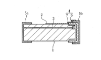
- FIG. 1 is a longitudinal sectional view schematically showing one embodiment (first embodiment) of an ultraviolet sensor according to the present invention
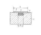
- FIG. 2 is a cross-sectional view of a main part of FIG.
- This ultraviolet sensor has a p-type semiconductor layer 1 whose main component is a solid solution of NiO and ZnO, and an n-type semiconductor layer 2 whose main component is ZnO.
- the n-type semiconductor layer 2 is a p-type semiconductor layer. 1 is bonded to the p-type semiconductor layer 1 with a part of the surface exposed.
- the p-type semiconductor layer 1 has a solid solution of NiO and ZnO as a main component and is represented by a general formula (Ni 1-x Zn x ) O (hereinafter referred to as (Ni, Zn) O). Can do.
- the Zn compounding molar ratio x is preferably 0.2 ⁇ x ⁇ 0.4 so that the p-type semiconductor layer 1 exhibits a desired function. If x is less than 0.2, the Ni content may be excessive and the resistance may be increased. On the other hand, if x exceeds 0.4, the Zn content will be excessive and ZnO particles may be produced. This is because there is a risk of precipitation at the crystal grain boundary and making it an n-type semiconductor.
- the p-type semiconductor layer 1 may contain other trace amounts of additives.
- it may contain Fe, Mn, or the like as a diffusing agent. Even if a trace amount of Zr, Si, or the like is contained as an impurity, it does not affect the characteristics.
- the n-type semiconductor layer 2 is mainly composed of ZnO, it is preferable to contain a trace amount of an additive, for example, Al, Co, In, Ga, etc. as a dopant, and to contain such a dopant. As a result, conductivity is imparted, and n-type semiconductorization is promoted.
- the n-type semiconductor layer 2 may also contain, for example, Fe, Ni, Mn or the like as a diffusing agent, and a trace amount of Zr, Si or the like as an impurity, like the p-type semiconductor layer 1. However, it does not affect the characteristics.
- the internal electrode 3 is embedded above the p-type semiconductor layer 1. Both ends of the internal electrode 3 are exposed at both end faces of the p-type semiconductor layer 1, and a high resistance layer 4 made of an insulating material is formed so as to cover one end of the internal electrode 3.
- the first external electrode 5 a is electrically connected to the other end of the internal electrode 3, and the second external electrode 5 b is electrically connected to the n-type semiconductor layer 2.
- the first and second external electrodes 5a and 5b are made of Ag, Ag-Pd, or the like. Although not shown, Ni and Ni are formed on the surfaces of the first and second external electrodes 5a and 5b.
- a first plating film made of, for example, and a second plating film made of Sn, etc. are sequentially formed, thereby constituting a terminal electrode.
- the high resistance layer 4 includes a first high resistance layer 6 made of the insulating material interposed between the second external electrode 5 b and the p-type semiconductor layer 1, and one end of the internal electrode 3.
- the insulating material has a second high resistance layer 7 diffused in the p-type semiconductor layer 1 so as to cover it.
- the internal electrode 3 has a low resistance containing an oxide having a perovskite structure represented by a general formula RNiO 3 or an oxide represented by a general formula R 2 NiO 4. It is formed with the complex oxide.
- the complex oxide mainly composed of the rare earth element R and Ni is a Ni-based oxide like (Ni, Zn) O, both of which are close in energy level and between (Ni, Zn) O. Therefore, it is possible to suppress the formation of an unnecessary Schottky barrier, which is close to ohmic contact.
- rare earth elements are less likely to diffuse to the (Ni, Zn) O side than Ni and have no oxygen releasing action like Pd, so that the specific resistance of (Ni, Zn) O can be reduced. Become.
- the composite oxide containing the rare earth elements R and Ni as the main components is a Ni-based oxide similar to (Ni, Zn) O, so that the shrinkage behavior at a high temperature is (Ni, Zn). Close to O, delamination is unlikely to occur between the p-type semiconductor layer 1 and the internal electrode 3, and there is no phenomenon of drawing the electrode into the sintered body.
- the specific resistance of (Ni, Zn) O can be reduced by making the internal electrode 3 mainly composed of the rare earth element R and Ni. Therefore, it is not necessary to provide an external power supply circuit and detect the change in the resistance value of the ultraviolet intensity, and a desired large photocurrent can be directly detected.
- the insulating material is likely to diffuse into the crystal grain boundary on the surface of the internal electrode 3, unlike the case of forming the metal alone.
- the surface parallel to the n-type semiconductor layer 2 of the internal electrode 3 has more pores than the surface perpendicular to the surface, and is easily diffused.
- the present embodiment contains an oxide having a perovskite structure represented by the general formula RNiO 3 and an oxide represented by the general formula R 2 NiO 4 , which are mainly composed of rare earth elements R and Ni.
- the internal electrode 3 is formed of a low resistance composite oxide.
- Such a rare earth element is not particularly limited as long as it has a low resistance when a composite oxide is formed with Ni.
- La, Pr, Nd, Sm, Gd, Dy, Ho , Er, and Yb can be used. Of these, it is preferable to use inexpensive La for economic reasons.
- the width dimension X of the n-type semiconductor layer 2 along the end face direction of the p-type semiconductor layer 1 is larger than the width dimension Y of the internal electrode 3 arranged to face the n-type semiconductor layer 2 as shown in FIG. Is also formed wide.
- the width dimension X of the n-type semiconductor layer 2 along the end face direction of the p-type semiconductor layer 1 is larger than the width dimension Y of the internal electrode 3 arranged to face the n-type semiconductor layer 2 as shown in FIG. Is also formed wide.
- both ends of the internal electrode 3 are exposed to both end surfaces of the p-type semiconductor layer 1 and the high resistance layer 4 (first and second) is covered so as to cover one end of the internal electrode 3.
- High resistance layers 6 and 7) are formed, the overlapping area between the internal electrode 3 and the n-type semiconductor layer 2 arranged in opposition is stabilized between products, and variation in characteristics is suppressed.
- an ultraviolet sensor capable of detecting a highly reliable photovoltaic power.
- the high resistance layer 4 (first and second high resistance layers 6 and 7) is provided, the insulating properties of the end portion of the internal electrode 3 and the vicinity thereof are improved, and thereby the ultraviolet rays are improved.
- the current leaking from the internal electrode 3 to the second external electrode 5b during non-irradiation can be suppressed, and the dark current can be reduced.
- the ultraviolet sensor When the ultraviolet sensor is mounted on the circuit board, it is usually necessary to select the direction. Therefore, it is also preferable to color the high resistance layer 4 by adding a color former. By coloring in this way, the directionality of the product can be easily confirmed. For example, the high resistance layer 4 becomes dark when Co 2 O 3 is contained, and becomes whitish when Al 2 O 3 is contained. Therefore, by including such a color former in the high resistance layer 4, the directionality can be easily recognized.
- the insulating material forming the high resistance layer 4 is not particularly limited as long as it is a material that reacts to some extent with (Ni, Zn) O forming the p-type semiconductor layer 1 and can be bonded or becomes a high resistance body.
- an insulating glass material such as a Si—B—Bi—Zn-based glass material can be preferably used.
- ZnO sintered body ZnO powder, various dopants, and additives such as a diffusing agent as necessary are prepared and weighed in predetermined amounts. Then, a solvent such as pure water is added to these weighed materials, and cobblestones such as PSZ (partially stabilized zirconia) are used as a grinding medium, and the mixture is sufficiently wet-mixed using a ball mill to obtain a slurry-like mixture. Next, this slurry-like mixture is dehydrated and dried, granulated to a predetermined particle size, and then calcined at a predetermined temperature for about 2 hours to obtain a calcined powder.
- a solvent such as pure water is added to these weighed materials, and cobblestones such as PSZ (partially stabilized zirconia) are used as a grinding medium, and the mixture is sufficiently wet-mixed using a ball mill to obtain a slurry-like mixture.
- this slurry-like mixture is dehydrated and dried, granul
- a solvent such as pure water is again added to the calcined powder obtained in this manner, and cobblestone is used as a grinding medium, and the mixture is sufficiently wet-ground using a ball mill to obtain a slurry-like pulverized product.
- pure water, a dispersant, a binder, a plasticizer, and the like are added to prepare a molding slurry.
- the forming slurry is formed using a forming method such as a doctor blade method to produce a ZnO green sheet having a predetermined film thickness.
- a predetermined number of these ZnO green sheets are laminated and pressed to produce a pressed body.
- the pressure-bonded body is degreased and fired to obtain a ZnO sintered body.
- NiO powder and ZnO powder are weighed so that the compounding molar ratio x of Zn is 0.2 to 0.4, a solvent such as pure water is added to the weighed product, and the ball is used as a grinding medium to sufficiently Mix and pulverize in a wet manner to obtain a slurry mixture.
- the mixture is dehydrated and dried, granulated to a predetermined particle size, and calcined at a predetermined temperature for about 2 hours to obtain a calcined powder.
- a solvent such as pure water is added again to the calcined powder thus obtained, and the mixture is sufficiently pulverized in a ball mill using cobblestone as a pulverizing medium to obtain a slurry pulverized product.
- this slurry-like pulverized product is dehydrated and dried, and then an organic solvent, a dispersant, a binder, a plasticizer, and the like are added to produce a molding slurry.
- the forming slurry is formed using a forming method such as a doctor blade method, thereby obtaining a (Ni, Zn) O green sheet having a predetermined film thickness.
- NiO powder and R 2 O 3 powder (R: rare earth element) are weighed so that the molar ratio is 2: 1, a solvent such as pure water is added to the weighed material, and a ball stone is used as a grinding medium in a ball mill. Thoroughly mix and pulverize in a wet manner to obtain a slurry mixture. Next, the slurry mixture is dehydrated and dried, granulated to a predetermined particle size, and calcined at a predetermined temperature for about 2 hours to obtain a calcined powder.
- a solvent such as pure water is added again to the calcined powder thus obtained, and the mixture is sufficiently pulverized in a ball mill using cobblestone as a pulverizing medium to obtain a slurry pulverized product.
- the slurry-like pulverized product is dehydrated and dried to obtain a composite oxide powder containing an oxide represented by the general formula RNiO 3 or the general formula R 2 NiO 4 .
- the obtained composite oxide powder is mixed with an organic vehicle and kneaded with a three-roll mill, thereby producing an internal electrode forming conductive paste.
- the organic vehicle is prepared such that the binder resin is dissolved in an organic solvent, and the binder resin and the organic solvent are, for example, in a volume ratio of 1 to 3: 7 to 9.
- the binder resin is not particularly limited, and for example, ethyl cellulose resin, nitrocellulose resin, acrylic resin, alkyd resin, or a combination thereof can be used.
- the organic solvent is not particularly limited, and ⁇ -terpineol, xylene, toluene, diethylene glycol monobutyl ether, diethylene glycol monobutyl ether acetate, diethylene glycol monoethyl ether, diethylene glycol monoethyl ether acetate, etc. alone or in combination thereof Can be used.
- insulating paste An insulating material such as a B—Si—Zn—Bi glass material is prepared, and if necessary, a coloring agent such as Co 2 O 3 or Al 2 O 3 is added to the insulating material, and this is combined with an organic vehicle. And kneading with a three-roll mill, thereby producing an insulating paste.
- the organic vehicle can use the same thing as what was used at the time of preparation of the electroconductive paste for internal electrode formation.
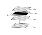
- a predetermined number of (Ni, Zn) O green sheets 8a, 8b, 8c,... 8n are prepared, and internal electrode forming conductivity is formed between both end faces of one (Ni, Zn) O green sheet 8b.
- a paste is applied to form an internal conductive film 9.
- a predetermined number of (Ni, Zn) O green sheets 8c to 8n having no conductive film formed thereon are stacked, and a (Ni, Zn) O green sheet 8b having an internal conductive film 9 formed thereon is stacked thereon. Further, a (Ni, Zn) O green sheet 8a on which a conductive film is not formed is laminated thereon and pressed to produce a laminate.
- the laminated body is sufficiently degreased at a temperature of 300 to 500 ° C., and then fired at a temperature of around 1200 ° C., whereby the conductive film 9 and the (Ni, Zn) O green sheets 8a to 8n are simultaneously fired, thereby A p-type semiconductor layer 1 having 3 embedded therein is obtained.
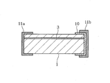
- the insulating paste is applied to one end surface of the p-type semiconductor layer 1 to form an insulating coating film 10, and the other end surface of the p-type semiconductor layer 1 and the insulating coating film 10 are formed.
- An external electrode forming conductive paste (second conductive paste) is applied to the outer surface of the first and second external conductive films 11a and 11b. And this is baked, thereby forming the first and second external electrodes 5a and 5b, and the insulating coating 10 diffuses toward the p-type semiconductor layer 1 side including the end of the internal electrode 3,
- the resistance layer 4 (first and second high resistance layers 6 and 7) is formed.
- the conductive material of the conductive paste for forming an external electrode is not particularly limited as long as it has good conductivity, and Ag, Ag—Pd, or the like can be used.
- Electrolytic plating is performed on the first and second external electrodes 5a and 5b to form a two-layered plating film composed of a first plating film and a second plating film, thereby forming a terminal electrode.
- n-type semiconductor layer 2 Sputtering is performed through a metal mask having a predetermined opening with a ZnO sintered body as a target so that a part of the p-type semiconductor layer 1 is exposed on the surface and electrically connected to the external electrode 5b. An n-type semiconductor layer 2 made of a ZnO-based thin film is formed on the surface of the p-type semiconductor layer 1, thereby obtaining an ultraviolet sensor.
- the conductive film 9 is formed by applying the conductive paste for forming an internal electrode between both end faces of one green sheet 8b.
- An insulating paste is applied to one end of the p-type semiconductor layer 1 and baked to diffuse the insulating material into the p-type semiconductor layer 1 and cover one end of the internal electrode 3 Since the high resistance layer 4 (first and second high resistance layers 6 and 7) is formed in the form, the insulation at one end portion of the internal electrode 3 and its periphery is improved, and the leakage current when no ultraviolet rays are irradiated Is suppressed and the dark current decreases.
- the insulating material is likely to diffuse into the crystal grain boundaries in the internal electrode 3 as described above.
- a plane parallel to the n-type semiconductor layer 2 of the internal electrode 3 has more pores than a plane perpendicular to the n-type semiconductor layer 2 and is easily diffused.
- the insulating material is easily diffused in the end portion of the internal electrode 3 and in the p-type semiconductor layer 1 in the vicinity thereof, and the end portion of the internal electrode 3 and the vicinity thereof are easily increased in resistance.
- the current leaking from the internal electrode 3 to the second external electrode 5b when not irradiated with ultraviolet rays can be reduced.
- the dark current can be more effectively suppressed and the sensor performance is excellent.
- An ultraviolet sensor can be obtained.
- FIG. 5 is a cross-sectional view of an essential part showing a second embodiment of the ultraviolet sensor.
- the internal electrode 12 is embedded in the p-type semiconductor layer 13 so that the plane area of the main surface of the internal electrode 12 is the same as the plane area of the main surface of the p-type semiconductor layer 13. ing.
- the width dimension U of the internal electrode along the end face of the p-type semiconductor layer 13 is wider than the width dimension V of the n-type semiconductor layer 14 arranged to face the internal electrode 12. Is formed.
- the width dimension U of the internal electrode along the end face of the p-type semiconductor layer 13 is larger than the width dimension V of the n-type semiconductor layer 14 arranged to face the internal electrode 12. Since it is formed wide, even if there is a dimensional variation in the n-type semiconductor layer 14, the area of the overlapping portion indicated by B in the figure, that is, the overlapping area can be increased. Therefore, it is possible to further improve the response intensity as well as stabilizing the photovoltaic power against ultraviolet irradiation.
- the laminate can be easily manufactured as shown in FIG.
- pure water is added again to the composite oxide powder, and the mixture is sufficiently mixed and ground in a ball mill together with a grinding medium to obtain a mixture.
- an organic solvent and a dispersant are added and mixed, and a binder and a plasticizer are added as appropriate to prepare a slurry.
- a doctor blade method is applied to the slurry to obtain a predetermined thickness.
- a conductive sheet is prepared.
- a predetermined number of (Ni, Zn) O green sheets 14b to 14n are laminated, a conductive sheet 15 as a conductive film is laminated thereon, and further, a (Ni, Zn) O green sheet 14a is laminated thereon.
- a predetermined number of (Ni, Zn) O green sheets 14b to 14n are laminated, a conductive sheet 15 as a conductive film is laminated thereon, and further, a (Ni, Zn) O green sheet 14a is laminated thereon.
- this laminated body is fired under the same conditions as in the first embodiment, whereby the p-type semiconductor layer 13 in which the internal electrode 12 is embedded can be obtained.
- the ultraviolet sensor of the second embodiment can be produced by the same method and procedure as in the first embodiment.
- the conductive powder is slurried and then molded to produce the conductive sheet 15 which is a conductive film. Therefore, screen printing is performed on the (Ni, Zn) O green sheet. Therefore, it is not necessary to form a conductive film having a predetermined pattern, and the ultraviolet sensor can be easily manufactured. Moreover, since the conductive sheet 15 which is a conductive film is formed by the sheet method, it can be formed thicker than the printing method. Therefore, the resistance of the internal electrode 12 is reduced, and as a result, the output current is increased and the sensor performance can be improved.
- FIG. 7 is a longitudinal sectional view showing the third embodiment.
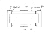
- FIG. 8 is a plan view of the third embodiment, and
- FIG. 9 is a front view of the third embodiment.
- the main surface has an internal electrode 18 having the same plane area as that of the p-type semiconductor layer 17, and the first high electrode is formed at both ends of the internal electrode 18.
- High resistance layers 21a and 21b including resistance layers 19a and 19b and second high resistance layers 20a and 20b are formed, and first and second external electrodes 22a are formed on the outer surfaces of the first high resistance layers 19a and 19b. 22b are formed.
- the n-type semiconductor layer 23 is suspended between the first external electrode 22a and the second external electrode 22b, and third electrodes 24a and 24b are formed on both side surfaces of the p-type semiconductor layer 17.
- the third electrodes 24a, 24b and the internal electrode 18 are electrically connected.
- the first external electrode 22a and the third external electrodes 24a and 24b, or the second external electrode 22b and the second The photocurrent can also be detected between the three external electrodes 24a and 24b, and a structure without directionality can be obtained even after mounting on the circuit board.
- the effective distance between the external electrodes for detecting the photocurrent is also shortened and the resistance is reduced, it is possible to further improve the response sensitivity to the ultraviolet intensity.
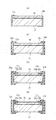
- FIG. 10 is a diagram showing a manufacturing method according to the third embodiment.
- the p-type semiconductor layer 17 in which the internal electrode 18 is embedded is manufactured by the same method and procedure as in the second embodiment.
- an insulating paste is produced by the same method and procedure as in the first embodiment.
- an insulating paste is apply
- external conductive films 26a and 26b are formed by applying an external electrode conductive paste on the outer surfaces of the insulating coatings 25a and 25b.
- a third external conductive film (not shown) is formed by applying a conductive paste for external electrodes to both side surfaces.
- a baking process is performed.
- the insulating coatings 25a and 25b diffuse into the p-type semiconductor layer 17, and as shown in FIG. 10C, the first and second external electrodes 22a and 22b and the third external electrode are formed.
- high resistance layers 21a and 21b first high resistance layers 19a and 19b and second high resistance layers 20a and 20b
- the surfaces of the first and second external electrodes 22a, 22b and the third external electrode are subjected to electrolytic plating to form a plating film, which is omitted in the drawing.
- sputtering is performed so that the ZnO sintered body is suspended between the first external electrode 22a and the second external electrode 22b as shown in FIG. As shown in d), an n-type semiconductor layer 23 is produced, and thereby a three-terminal ultraviolet sensor is produced.
- the effective distance between the external electrodes for detecting the photocurrent is shorter than that in the first and second embodiments, the response intensity to the ultraviolet intensity is better, and the dark current is reduced.
- a low-reliability and good UV sensor can be easily obtained.
- the present invention is not limited to the above embodiment.
- the high-resistance layers 4, 21 a, 21 b and the external electrodes 5 a, 5 b, 22 a, 22 b are obtained by simultaneously firing the insulating coating film and the external conductive film. Good.
- the first high resistance layers 6, 19 a, 19 b are formed on the end surfaces and the end surface folded portions of the p-type semiconductor layers 1, 17, but cover the end portions of the internal electrodes 3, 18. If possible, the desired insulation can be improved, so that the first high resistance layer may be formed only on the end face.
- a conductive paste for forming an internal electrode containing a composite oxide is prepared, and the conductive paste for forming an internal electrode is applied to the surface of a (Ni, Zn) O green sheet, and then Although the internal electrode 3 is formed by firing, a rare earth paste whose main component is composed of the rare earth oxide R 2 O 3 is prepared without including Ni in the internal electrode forming paste, and is fired.
- a desired internal electrode can also be formed by diffusing Ni in the (Ni, Zn) O green sheet into the rare earth film side.
- Example preparation (Sample No. 1) [Preparation of ZnO sintered body] ZnO as a main component and Ga 2 O 3 as a dopant were weighed so that the compounding ratio was 99.9 mol% and 0.1 mol%, respectively, in mol%. Then, pure water was added to these weighed products, and the mixture was pulverized in a ball mill using PSZ beads as a pulverization medium to obtain a slurry mixture having an average particle size of 0.5 ⁇ m or less. Next, this slurry-like mixture was dehydrated and dried, granulated to a particle size of about 50 ⁇ m, and calcined at a temperature of 1200 ° C. for 2 hours to obtain a calcined powder.
- a predetermined number of the green sheets were laminated so as to have a thickness of 20 mm, and a pressure-bonding treatment was performed for 5 minutes at a pressure of 250 MPa, to obtain a pressure-bonded body.
- the pressure-bonded body was degreased and then fired at a temperature of 1200 ° C. for 20 hours to obtain a ZnO sintered body.
- NiO powder and ZnO powder were weighed so as to have a molar ratio of 7: 3, pure water was added thereto, and the mixture was pulverized with a ball mill using PSZ beads as a pulverization medium to obtain a slurry mixture. Next, this slurry-like mixture was dehydrated and dried, granulated to a particle size of about 50 ⁇ m, and calcined at a temperature of 1200 ° C. for 2 hours to obtain a calcined powder.
- NiO powder and La 2 O 3 powder as a rare earth oxide were weighed so as to have a molar ratio of 2: 1, respectively, pure water was added to the weighed material, and the mixture was pulverized in a ball mill using PSZ beads as a grinding medium. A slurry mixture was obtained. Next, this slurry-like mixture was dehydrated and dried, granulated to a particle size of about 50 ⁇ m, and calcined at a temperature of 1200 ° C. for 2 hours to obtain a calcined powder.
- the organic vehicle was prepared by mixing ethyl cellulose resin and ⁇ -terpineol so as to be 30% by volume of ethyl cellulose resin as the binder resin and 70% by volume of ⁇ -terpineol as the organic solvent.
- the laminate was placed on a ZrO 2 setter, placed in a firing furnace, degreased slowly and sufficiently at a temperature of 300 ° C., and then fired in the air at a temperature of 1200 ° C. for 1 hour. A semiconductor layer was obtained.
- Electroplating was applied to the surfaces of the first and second external electrodes to sequentially form a Ni film and a Sn film, thereby producing a terminal electrode.
- n-type semiconductor layer Sputtering is performed using a ZnO sintered body as a target, using a metal mask so as to cover a part of one main surface of the p-type semiconductor layer and to overlap a part of the second external electrode. An n-type semiconductor layer having a predetermined pattern of .5 ⁇ m was produced, thereby obtaining a sample of sample number 1.
- NiO powder and La 2 O 3 powder as a rare earth oxide were weighed so as to have a molar ratio of 2: 1, respectively, pure water was added to the weighed material, and the mixture was pulverized in a ball mill using PSZ beads as a grinding medium. A slurry mixture was obtained. Next, this slurry-like mixture was dehydrated and dried, granulated to a particle size of about 50 ⁇ m, and calcined at a temperature of 1200 ° C. for 2 hours to obtain a calcined powder.
- Example No. 3 A p-type semiconductor layer was produced in the same manner as Sample No. 2. Further, an insulating paste was produced by the same method and procedure as in the first embodiment.
- an insulating paste was applied to both ends of the p-type semiconductor layer to form an insulating coating film.
- an external electrode forming conductive paste is applied to the outer surface of the insulating coating to form an external conductive film, and the external electrode forming conductive paste is applied to both sides of the p-type semiconductor layer. 3 external conductive films were formed.
- a baking process was performed at a temperature of 850 ° C. for 10 minutes, and a high resistance layer was formed simultaneously with the formation of the first and second external electrodes and the third external electrode.
- electrolytic plating was performed on the surface of each external electrode to sequentially form a Ni film and a Sn film, thereby forming each terminal electrode.
- Example No. 4 As a sample number 4, a conventional ultraviolet sensor described in Patent Document 1 (see FIG. 11) was produced.
- the laminate was placed on a ZrO 2 setter, placed in a firing furnace, degreased slowly and sufficiently at a temperature of 300 ° C., and then fired in the air at a temperature of 1200 ° C. for 1 hour.
- a p-type semiconductor layer was obtained.
- n-type semiconductor layer having a predetermined pattern of about 0.5 ⁇ m was produced, whereby a sample No. 4 was obtained.
- sample evaluation For each of the 30 samples of sample numbers 1 to 4, the irradiance is 1 mW / cm 2, and the wavelength of the light source is changed stepwise from 10 nm to 600 nm every 10 nm by an ultraviolet light source equipped with a spectroscope in a dark room, and n The wavelength response characteristics were examined by irradiating the outer surface of the mold semiconductor layer side and measuring the current flowing at both ends of the UV sensor.
- the peak wavelength at which the photocurrent is maximum the average value, maximum value, and minimum value of the light reception sensitivity (maximum light reception sensitivity) of this peak wavelength are obtained. Evaluated.
- Table 1 shows the measurement results of the samples Nos. 1 to 4.
- the measurement temperature was controlled to be 25 ° C. ⁇ 1 ° C. in all cases.
- Sample Nos. 1 to 4 all had a peak wavelength of 360 nm.
- sample No. 4 has a maximum light receiving sensitivity as low as 0.25 A / W, a variation in maximum light receiving sensitivity between samples is as large as 0.15 to 0.30 A / W, and a dark current is also as large as 0.05 nA. It was. This is because the tip of the internal electrode extends only to the center of the p-type semiconductor layer, resulting in dimensional variations in the internal electrodes between samples, resulting in variations in the overlapping area, and large variations in maximum light receiving sensitivity. It seems to have become. In addition, since sample No.
- Sample No. 2 has the same plane area of the main surface of the internal electrode as the plane area of the main surface of the p-type semiconductor layer, the overlapping area is large, and the resistance of the internal electrode is reduced. Compared to 1, the variation in the maximum light receiving sensitivity between samples was further reduced, the dark current was reduced, and the maximum light receiving sensitivity was increased.
- sample No. 3 is similar to sample No. 2 in that the plane area of the main surface of the internal electrode is the same as the plane area of the main surface of the p-type semiconductor layer, and the effective distance between the external electrodes for detecting the photocurrent. Since the resistance is reduced by shortening, the dark current can be further reduced compared to Sample No. 2, the maximum light receiving sensitivity is further increased, and the variation in the maximum light receiving sensitivity between samples is also good. I understood.
Landscapes
- Physics & Mathematics (AREA)
- General Physics & Mathematics (AREA)
- Spectroscopy & Molecular Physics (AREA)
- Electromagnetism (AREA)
- Light Receiving Elements (AREA)
- Engineering & Computer Science (AREA)
- Manufacturing & Machinery (AREA)
Abstract
NiOとZnOとの固溶体を主成分とするp型半導体層1と、p型半導体層1の一部が表面に露出した形態でp型半導体層1に接合されたZnOを主成分とするn型半導体層2と、n型半導体層2と対向状にp型半導体層1に埋設された内部電極3とを有している。内部電極3の両端は、p型半導体層1の両端面に露出されると共に、絶縁性材料からなる高抵抗層4(第1及び第2の高抵抗層6、7)が、内部電極3の一方の端部を覆うように形成されている。このうち第2の高抵抗層7は、第1の高抵抗層6からの絶縁性材料がp型半導体層1内に拡散されてなる。第1の外部電極5aは内部電極3の他方の端部と電気的に接続され、第2の外部電極5bはn型半導体層2と電気的に接続されている。これにより製品間における特性バラツキを抑制することができ、かつ暗電流も低く信頼性の良好な高感度、高出力の紫外線センサを実現する。
Description
本発明は、紫外線センサ、及び紫外線センサの製造方法に関し、より詳しくは、酸化化合物半導体を使用してp型半導体層とn型半導体層とをヘテロ接合させた積層構造を有するフォトダイオード型の紫外線センサ、及びその製造方法に関する。
紫外線センサは、空気中や水中に浮遊する菌を殺菌する殺菌灯や、紫外線照射装置等の紫外線検出デバイスとして広く使用されており、近年では光通信デバイスへの応用にも期待されている。
この種の紫外線センサは、従来より、センサ材料としてダイヤモンド半導体やSiC半導体を使用したものが知られている。しかしながら、これらのダイヤモンド半導体やSiC半導体は、材料加工性に劣り、高価であるという欠点があった。
そこで、最近では、材料加工性が容易で比較的安価な酸化化合物半導体が注目されており、これらの酸化化合物半導体を使用してp型半導体層とn型半導体層とをヘテロ接合させた紫外線センサの研究・開発が盛んに行なわれている。
例えば、特許文献1には、図11に示すように、ZnOがNiOに固溶してなる酸化化合物半導体からなる(Ni,Zn)O層101と、前記(Ni,Zn)O層101の一方主面102の一部を覆うように、スパッタリング法により形成される薄膜材料層103と、前記(Ni,Zn)O層101の両端に形成された第1及び第2の端子電極104a、104bとを有し、前記(Ni,Zn)O層101内に内部電極105が形成され、前記第1の端子電極104aが前記内部電極105に電気的に接続されると共に、前記第2の端子電極104bが前記薄膜材料層103に電気的に接続された紫外線センサが提案されている。
この特許文献1では、内部電極105は、一端が端子電極104aに電気的に接続されると共に、他端は(Ni,Zn)O層101内の略中央部まで延伸して形成されている。また、薄膜材料層103は内部電極105と対向状に配され、かつ平面視で一部が該内部電極105と重なるように形成されており、さらに該薄膜材料層103は他方の端子電極104bに接続されている。
そして、特許文献1では、図中上方から紫外線が照射され、(Ni,Zn)O層101と薄膜材料層103との接合界面に形成される空乏層に紫外光が当たると、キャリアが励起され、薄膜材料層103と内部電極105との重なり部分aで光起電力を発生する。
特許文献1では、上述したように薄膜材料層103と内部電極105との重なり部分aで紫外線強度に応じた光起電力を発生させており、したがって検出精度の信頼性を確保するためには、製品間でバラツキのない安定した受光感度を得る必要がある。
ところが、この種の紫外線センサでは、良好な生産性を確保する観点から、通常、大判の基板上にアレイ状に多数の素子を作製するいわゆる多数個取り方式が採用されている。このため、内部電極105をスクリーン印刷して形成しても、印刷やカッティングの際にバラツキが生じ易く、内部電極の長手方向や幅方向に寸法バラツキが生じ易い。
したがって、このような状況下でスパッタリング法により薄膜材料層103を形成した場合、内部電極105の長手方向及び幅方向の双方で重なり部分aにバラツキが生じ易くなる。しかも、薄膜材料層103はスパッタリング法で形成しているため、薄膜材料層103の寸法にもバラツキが生じ易い。したがって製品間で内部電極105と薄膜材料層103との重なり部分aの面積(以下、「重なり面積」という。)にバラツキが生じ易く、このため製品間で紫外光に対する応答強度にもバラツキが生じ易く、高精度に安定した信頼性を有する光起電力を得るのが困難である。
また、特許文献1のようなフォトダイオード型の紫外線センサの場合、(Ni,Zn)O層101と薄膜材料層103との間にはpn接合によってダイオードが形成されることから、内部電極105と第2の端子電極104bとの間には抵抗が形成されて閉回路を形成する。このため、紫外線非照射時に発生する微弱電流が前記閉回路を流れて内部電極105から端子電極104bにリークし、暗電流の増加を招くおそれがある。
本発明はこのような事情に鑑みなされたものであって、製品間における特性バラツキを抑制することができ、かつ暗電流も低く信頼性の良好な高感度、高出力の紫外線センサ及びその製造方法を提供することを目的とする。
上記目的を達成するために本発明に係る紫外線センサは、NiOとZnOとの固溶体を主成分とするp型半導体層と、該p型半導体層に接合されたZnOを主成分とするn型半導体層と、該n型半導体層と対向状に前記p型半導体層に埋設された内部電極とを有する紫外線センサにおいて、前記n型半導体層は、前記p型半導体層の一部が表面に露出した形態で前記p型半導体層に接合され、前記内部電極の両端が、前記p型半導体層の両端面に露出されると共に、絶縁性材料からなる高抵抗層が、前記内部電極の一方の端部を覆うように形成され、第1の外部電極が、前記内部電極の他方の端部と電気的に接続されると共に、第2の外部電極が、前記n型半導体層と電気的に接続されていることを特徴としている。
これにより内部電極はp型半導体層の一方の端面から他方の端面まで形成される。したがって製品間における内部電極の長手方向の寸法バラツキを抑制することができ、対向するn型半導体層との間で形成される重なり面積にバラツキが生じるのを低減することが可能となる。
また、本発明の紫外線センサは、前記高抵抗層が、前記第2の外部電極と前記p型半導体層との間に介在された前記絶縁性材料からなる第1の高抵抗層と、前記内部電極の前記一方の端部を覆うように前記絶縁性材料が前記p型半導体層内に拡散された第2の高抵抗層とを有しているのが好ましい。
これにより、内部電極の一方の端部が効果的に絶縁化された紫外線センサを得ることができる。
さらに、本発明の紫外線センサは、前記p型半導体層の端面方向に沿う前記n型半導体層の幅寸法は、該n型半導体層と対向状に配された前記内部電極の幅寸法よりも幅広に形成されているのが好ましい。
この場合は、内部電極の幅寸法がn型半導体層の幅寸法よりも小さくなることから、製品間における内部電極の幅方向の寸法バラツキもn型半導体層で吸収することが可能となる。したがって、重なり面積を製品間で全体的に安定化することができ、紫外線強度に対する製品間の応答バラツキを効果的に抑制することが可能となる。
また、本発明の紫外線センサは、前記p型半導体層の端面方向に沿う前記内部電極の幅寸法は、該内部電極と対向状に配された前記n型半導体層の幅寸法よりも幅広に形成されているのも好ましい。
この場合は、n型半導体層の幅寸法が内部電極の幅寸法よりも小さいことから、n型半導体層に寸法バラツキが生じても、内部電極からはみ出ることもなく、重なり面積を大きくとることができる。したがって紫外線照射に対する光起電力の安定化と共により一層応答強度の良好な紫外線センサを得ることが可能となる。
また、本発明の紫外線センサは、前記高抵抗層は、他の構成部位との識別が可能な色彩でカラーリングされているのが好ましい。
これにより回路基板に実装する場合の方向視認性が容易となり、したがって方向選別のための作業を軽減することが可能となり、低コスト化が可能となる。
また、本発明の紫外線センサは、前記内部電極は、希土類元素とNiとを主成分とした複合酸化物で形成されているのが好ましい。
また、本発明の紫外線センサは、前記内部電極は、希土類元素とNiとを主成分とした複合酸化物で形成されているのが好ましい。
これにより内部電極材料にPtやPd等の高価な貴金属材料を使用しなくてもよくなり、かつ、内部電極内への絶縁性材料の拡散も容易になることから、安価かつ高感度で信頼性の良好な紫外線センサを得ることができる。
また、本発明に係る紫外線センサは、NiOとZnOとの固溶体を主成分とするp型半導体層と、前記p型半導体層に接合されたZnOを主成分とするn型半導体層と、該n型半導体層と対向状に前記p型半導体層に埋設された内部電極とを有する紫外線センサにおいて、前記内部電極が、前記p型半導体層の両端面及び両側面に露出されると共に、絶縁性材料からなる高抵抗層が、前記内部電極の両端部を覆うように形成され、第1及び第2の外部電極が、前記高抵抗層の表面に形成されると共に、前記n型半導体層が、前記第1及び第2の外部電極と電気的に接続され、かつ、第3の外部電極が、前記p型半導体層の側面に形成されていることを特徴としている。
この場合も、上述と同様の作用効果を奏することができ、製品間で特性バラツキが抑制された紫外線センサを得ることができる。しかも、光起電力を取り出す外部電極間の実効距離を短くすることができるので、より一層出力電流を向上することができ、センサ性能がより一層向上した紫外線センサを得ることができる。また、回路基板に実装する場合も方向性を考慮する必要がない。
また、本発明の紫外線センサにおいても、前記高抵抗層は、前記第1及び第2の外部電極と前記p型半導体層との間にそれぞれ介在された前記絶縁性材料からなる第1の高抵抗層と、前記内部電極の前記両端部を覆うように前記絶縁性材料が前記p型半導体層内に拡散された第2の高抵抗層とを有しているのが好ましい。
さらに、本発明の紫外線センサにおいても、前記内部電極は、希土類元素とNiとを主成分とした複合酸化物で形成されているのが好ましい。
また、本発明に係る紫外線センサの製造方法は、NiOとZnOとの固溶体を主成分とするグリーンシートを複数作製するグリーンシート作製工程と、内部電極となるべき導電膜を形成する導電膜形成工程と、前記導電膜を挟持するような形態で前記複数のグリーンシートを積層し、積層体を作製する積層体作製工程と、前記積層体を焼成し、内部電極が埋め込まれたp型半導体層を形成するp型半導体層形成工程と、ZnOを主成分とするZnO焼結体をターゲットにしてスパッタリングし、n型半導体層を前記p型半導体層の表面に形成するn型半導体層形成工程とを含む紫外線センサの製造方法において、前記導電膜形成工程は、前記複数のグリーンシートのうち、一のグリーンシートの両端面間に第1の導電性ペーストを塗布して前記導電膜を形成すると共に、前記p型半導体層の一方の端部に絶縁性材料からなる絶縁性ペーストを塗布して焼成処理を行い、前記絶縁性材料を前記p型半導体層内に拡散させ、前記内部電極の一方の端部を覆うような形態で高抵抗層を形成する高抵抗層形成工程を有していることを特徴としている。
これにより内部電極の端部を含むp型半導体層内に絶縁性材料を容易に拡散させて前記内部電極の一方の端部を覆うことができ、内部電極の一方の端部を容易に絶縁化することができる。
また、本発明の紫外線センサの製造方法は、前記p型半導体層の他方の端部及び前記高抵抗層の外表面に第2の導電性ペーストを塗布して焼成処理を行い、第1及び第2の外部電極をそれぞれ形成する外部電極形成工程を有し、該外部電極形成工程における焼成処理と前記高抵抗層形成工程における焼成処理とを同時に行い、前記第1及び第2の外部電極と前記高抵抗層とを同時に作製するのが好ましい。
これにより大幅な工程増を招くこともなく、紫外線センサを効率良く製造することができる。
また、本発明の紫外線センサの製造方法は、前記高抵抗層形成工程は、前記絶縁性材料中に発色剤を添加するのが好ましい。
これにより方向視認性が良好で回路実装に好適な紫外線センサを容易に得ることができる。
また、本発明に係る紫外線センサの製造方法は、NiOとZnOとの固溶体を主成分とするグリーンシートを複数作製するグリーンシート作製工程と、内部電極となるべき導電膜を形成する導電膜形成工程と、前記導電膜を挟持するような形態で前記複数のグリーンシートを積層し、積層体を作製する積層体作製工程と、前記積層体を焼成し、内部電極が埋め込まれたp型半導体層を形成するp型半導体層形成工程と、ZnOを主成分とするZnO焼結体をターゲットにしてスパッタリングし、n型半導体層を前記p型半導体層の表面に形成するn型半導体層形成工程とを含む紫外線センサの製造方法において、前記導電膜形成工程は、導電性粉末をスラリー化した後成形し、シート状の導電膜である導電性シートを作製すると共に、前記p型半導体層の一方の端部に絶縁性材料からなる絶縁性ペーストを塗布して焼成処理を行い、前記絶縁性材料を前記p型半導体層内に拡散させ、前記内部電極の一方の端部を覆うような形態で高抵抗層を形成する高抵抗層形成工程を有していることを特徴としている。
これによりグリーンシート上にスクリーン印刷して導電膜を形成する必要がなく、シート成形のみで積層体を得ることが可能となる。
また、本発明の紫外線センサの製造方法は、前記p型半導体層の他方の端部及び前記高抵抗層の外表面に第2の導電性ペーストを塗布して焼成処理を行い、第1及び第2の外部電極を形成する外部電極形成工程を有し、該外部電極形成工程における焼成処理と前記高抵抗層形成工程における焼成処理とを同時に行い、前記各外部電極と前記高抵抗層とを同時に作製するのが好ましい。
また、本発明の紫外線センサの製造方法は、前記高抵抗層形成工程が、前記絶縁性材料中に発色剤を添加するのが好ましい。
また、本発明に係る紫外線センサの製造方法は、NiOとZnOとの固溶体を主成分とするグリーンシートを複数作製するグリーンシート作製工程と、内部電極となるべき導電膜を形成する導電膜形成工程と、前記導電膜を挟持するような形態で前記複数のグリーンシートを積層し、積層体を作製する積層体作製工程と、前記積層体を焼成し、内部電極が埋め込まれたp型半導体層を形成するp型半導体層形成工程と、ZnOを主成分とするZnO焼結体をターゲットにしてスパッタリングし、n型半導体層を前記p型半導体層の表面に形成するn型半導体層形成工程とを含む紫外線センサの製造方法において、前記導電膜形成工程は、導電性粉末をスラリー化した後成形し、シート状の導電膜である導電性シートを作製すると共に、前記p型半導体層の両端部に絶縁性材料からなる絶縁性ペーストを塗布して焼成処理を行い、前記絶縁性材料を前記p型半導体層内に拡散させ、前記内部電極の両端部を覆うような形態で高抵抗層を形成する高抵抗層形成工程と、前記高抵抗層の外表面及び前記p型半導体層の側面に第2の導電性ペーストを塗布して焼成処理を行い、第1及び第2の外部電極、及び第3外部電極を形成する外部電極形成工程を有していることを特徴としている。
これにより製品間の特性バラツキが小さく、出力電流がより一層向上した高感度の三端子用の紫外線センサを容易に得ることができる。
また、本発明の紫外線センサの製造方法は、前記外部電極形成工程における焼成処理と前記高抵抗層形成工程における焼成処理を同時に行い、前記各外部電極と前記高抵抗層とを同時に作製するのが好ましい。
本発明の紫外線センサによれば、n型半導体層は、p型半導体層の一部が表面に露出した形態で前記p型半導体層に接合され、内部電極の両端が、前記p型半導体層の両端面に露出されると共に、絶縁性材料からなる高抵抗層が、前記内部電極の一方の端部を覆うように形成され、第1の外部電極が、前記内部電極の他方の端部と電気的に接続されると共に、第2の外部電極が、前記n型半導体層と電気的に接続されているので、内部電極はp型半導体層の一方の端面から他方の端面まで形成されることとなり、これにより製品間における内部電極の長手方向の寸法バラツキを抑制することができ、対向するn型半導体層との間で形成される重なり面積にバラツキが生じるのを低減することが可能となる。すなわち、重なり面積が安定化することから、製品間における紫外線強度に対する検出感度のバラツキを抑制することができ、良好な信頼性を有する高感度の紫外線センサを得ることが可能となる。また、高抵抗層が、前記内部電極の一方の端部を覆うことから、内部電極の端部が高度に絶縁化され、これにより紫外線非照射時に内部電極から第2の外部電極にリークする電流が抑制され、暗電流を低減することが可能となり、センサ性能の向上を図ることができる。
また、本発明の紫外線センサによれば、内部電極が、前記p型半導体層の両端面及び両側面に露出されると共に、絶縁性材料からなる高抵抗層が、前記内部電極の両端部を覆うように形成され、第1及び第2の外部電極が、前記高抵抗層の表面に形成されると共に、前記n型半導体層が、前記第1及び第2の外部電極と電気的に接続され、かつ、第3の外部電極が、前記p型半導体層の側面に形成されているので、三端子用の紫外線センサの場合も、上述と同様の作用効果を奏することができ、製品間で特性バラツキが抑制された紫外線センサを得ることができる。しかも、この場合は、光起電力を取り出す外部電極間の実効距離を短くすることができるので、より一層出力電流を向上することができ、センサ性能がより一層向上した紫外線センサを得ることができる。また、回路基板に実装する場合も方向性を考慮する必要がない。
また、本発明の紫外線センサの製造方法によれば、導電膜形成工程は、複数のグリーンシートのうち、一のグリーンシートの両端面間に第1の導電性ペーストを塗布して導電膜を形成すると共に、p型半導体層の一方の端部に絶縁性材料からなる絶縁性ペーストを塗布して焼成処理を行い、前記絶縁性材料を前記p型半導体層内に拡散させ、前記内部電極の一方の端部を覆うような形態で高抵抗層を形成する高抵抗層形成工程を有しているので、内部電極の端部を含むp型半導体層内に絶縁性材料を容易に拡散させて前記内部電極の一方の端部を覆うことができ、これにより内部電極の一方の端部を容易に絶縁化することができる。
また、本発明の紫外線センサの製造方法によれば、導電膜形成工程は、導電性粉末をスラリー化した後成形し、シート状の導電膜である導電性シートを作製すると共に、前記p型半導体層の一方の端部に絶縁性材料からなる絶縁性ペーストを塗布して焼成処理を行い、前記絶縁性材料を前記p型半導体層内に拡散させ、前記内部電極の一方の端部を覆うような形態で高抵抗層を形成する高抵抗層形成工程を有しているので、グリーンシート上にスクリーン印刷して導電膜を形成する必要がなく、シート成形のみで積層体を得ることが可能となる。すなわち、この場合、導電膜をシート工法で形成するので、印刷工法に比べて厚膜に形成することができ、その結果、内部電極の抵抗が低減し、これにより出力電流も向上し、センサ性能が向上する。
また、本発明の紫外線センサの製造方法によれば、導電膜形成工程は、導電性粉末をスラリー化した後成形し、シート状の導電膜である導電性シートを作製すると共に、前記p型半導体層の両端部に絶縁性材料からなる絶縁性ペーストを塗布して焼成処理を行い、前記絶縁性材料を前記p型半導体層内に拡散させ、前記内部電極の両端部を覆うような形態で高抵抗層を形成する高抵抗層形成工程と、前記高抵抗層の外表面及び前記p型半導体層の側面に第2の導電性ペーストを塗布して焼成処理を行い、第1及び第2の外部電極、及び第3外部電極を形成する外部電極形成工程を有しているので、製品間の特性バラツキが小さく、出力電流がより一層向上した高感度の三端子用の紫外線センサを容易に得ることができる。
次に、本発明の実施の形態を添付図面を参照しながら詳説する。
図1は、本発明に係る紫外線センサの一実施の形態(第1の実施の形態)を模式的に示す縦断面図であり、図2は図1の要部横断面図である。
この紫外線センサは、NiOとZnOとの固溶体を主成分とするp型半導体層1と、ZnOを主成分とするn型半導体層2とを有し、n型半導体層2は、p型半導体層1の表面の一部が露出した形態でp型半導体層1に接合されている。
p型半導体層1は、上述したようにNiOとZnOとの固溶体を主成分とし、一般式(Ni1-xZnx)O(以下、(Ni,Zn)Oと表記する。)で表わすことができる。Znの配合モル比xは、p型半導体層1が所望の機能を発揮するためには、0.2≦x≦0.4が好ましい。これはxが0.2未満になると、Niの含有量が過剰となって高抵抗化するおそれがあり、一方、xが0.4を超えると、Znの含有量が過剰となってZnO粒子が結晶粒界に析出し、n型に半導体化してしまうおそれがあるからである。尚、p型半導体層1には、その他の微量の添加物が含まれていてもよく、例えば、拡散剤として、Fe、Mn等を含有していてもよい。また、不純物として微量のZr、Si等を含有していても特性に影響を与えるものではない。
n型半導体層2は、ZnOを主成分とするのであれば、微量の添加剤、例えば、ドープ剤としてAl、Co、In、Ga等を含有するのも好ましく、斯かるドープ剤を含有することにより導電性が付与され、n型に半導体化が促進される。また、このn型半導体層2も、p型半導体層1と同様、例えば拡散剤として、Fe、Ni、Mn等を含有していてもよく、また不純物として微量のZr、Si等を含有していても特性に影響を与えるものではない。
p型半導体層1の上部には内部電極3が埋設されている。内部電極3の両端は、p型半導体層1の両端面に露出されると共に、絶縁性材料からなる高抵抗層4が、内部電極3の一方の端部を覆うように形成されている。
そして、第1の外部電極5aが、内部電極3の他方の端部と電気的に接続されると共に、第2の外部電極5bが、n型半導体層2と電気的に接続されている。尚、第1及び第2の外部電極5a、5bは、AgやAg-Pd等で形成され、また、図示はしていないが、第1及び第2の外部電極5a、5bの表面にはNi等からなる第1のめっき皮膜及びSn等からなる第2のめっき皮膜が順次形成され、これにより端子電極を構成している。
上記高抵抗層4は、第2の外部電極5bとp型半導体層1との間に介在された前記絶縁性材料からなる第1の高抵抗層6と、内部電極3の一方の端部を覆うように前記絶縁性材料が前記p型半導体層1内に拡散された第2の高抵抗層7とを有している。
また、上記内部電極3は、希土類元素RとNiを主成分とした一般式RNiO3で表されるペロブスカイト型構造の酸化物や一般式R2NiO4で表される酸化物を含有する低抵抗の複合酸化物で形成されている。
すなわち、希土類元素RとNiを主成分とした複合酸化物は、(Ni,Zn)Oと同様、Ni系酸化物であり、両者はエネルギー準位が近く、(Ni,Zn)Oとの間で不必要なショットキー障壁が形成されるのを抑制でき、オーミック接触に近くなる。また、希土類元素は、Niに比べ、(Ni,Zn)O側に拡散しにくく、Pdのような酸素放出作用もないことから、(Ni,Zn)Oの比抵抗を低下させることが可能となる。しかも、上述したように希土類元素RとNiを主成分とした複合酸化物は、(Ni,Zn)Oと同様のNi系酸化物であることから、高温での収縮挙動が(Ni,Zn)Oと近く、p型半導体層1と内部電極3との間でデラミネーションが生じ難く、焼結体内部に電極を引き込むような現象もない。
このように内部電極3を希土類元素RとNiを主成分とすることにより(Ni,Zn)Oの比抵抗を低下させることができる。したがって、外部に電源回路を設けて紫外線強度の抵抗値の変化で検出する必要がなく、所望の大きな光電流を直接検知することが可能となる。
しかも、内部電極3を上述のような複合酸化物で形成することにより、金属単体で形成した場合とは異なり、内部電極3表面の結晶粒界に絶縁性材料が拡散し易くなる。特に、内部電極3のn型半導体層2と平行な面は、それと垂直な面より気孔が多く、拡散し易くなる。このように内部電極を複合酸化物で形成することにより、前記絶縁性材料は内部電極3の端部内及び端部近傍のp型半導体層1内に容易に拡散し、これにより内部電極3の端部及びその近傍領域は容易に高抵抗化する。そしてその結果、紫外線非照射時に内部電極3から第2の外部電極5bにリークする電流を効果的に低減させることが可能となり、暗電流の低減化を図ることが可能となる。
また、この場合、Pt、Pd等の高価な貴金属材料を使用しなくて済むので、高価格化を抑制することが可能となる。
以上の理由から本実施の形態では、希土類元素RとNiを主成分とした一般式RNiO3で表されるペロブスカイト型構造の酸化物や一般式R2NiO4で表される酸化物を含有する低抵抗の複合酸化物で内部電極3を形成している。
このような希土類元素としては、Niとの間で複合酸化物を形成した場合に低抵抗であれば、特に限定されるものではなく、例えば、La、Pr、Nd、Sm、Gd、Dy、Ho、Er、及びYbの中から選択された少なくとも1種を使用することができる。尚、これらの中では、経済的理由から安価なLaを使用するのが好ましい。
そして、p型半導体層1の端面方向に沿うn型半導体層2の幅寸法Xは、図2に示すように、n型半導体層2と対向状に配された内部電極3の幅寸法Yよりも幅広に形成されている。そして、これにより内部電極3の長手方向のみならず幅方向のバラツキもn型半導体層2で吸収することが可能となる。すなわち、対向状に配された内部電極3とn型半導体層2との重なり部分(図2中、「A」で示す。)の面積(重なり面積)が製品間で安定化し、製品間の特性バラツキをより抑制することが可能となる。
このように本実施の形態では、内部電極3の両端をp型半導体層1の両端面に露出させると共に、内部電極3の一方の端部を覆うように高抵抗層4(第1及び第2の高抵抗層6、7)を形成しているので、対向状に配された内部電極3とn型半導体層2との間の重なり面積が製品間で安定化したものとなり、特性バラツキが抑制された信頼性の良好な光起電力の検出が可能な紫外線センサを得ることができる。
また、上述したように高抵抗層4(第1及び第2の高抵抗層6、7)を有しているので、内部電極3の端部及びその近傍の絶縁性が向上し、これにより紫外線非照射時における内部電極3から第2の外部電極5bにリークする電流を抑制することができ、暗電流の低減化が可能となる。
また、紫外線センサを回路基板上に実装する場合、通常は、方向選別が必要になることから、高抵抗層4に発色剤を含有させてカラーリングするのも好ましい。このようにカラーリングすることにより、製品の方向性の確認が容易となる。例えば、Co2O3を含有させることで高抵抗層4が黒っぽくなり、Al2O3を含有させることで白っぽくなる。したがって、このような発色剤を高抵抗層4に含有させることにより、方向性の視認が容易になる。
尚、高抵抗層4を形成する絶縁性材料としては、p型半導体層1を形成する(Ni,Zn)Oとある程度反応し、接合できる絶縁体又は高抵抗体となる材料であれば特に限定されるものではないが、Si-B-Bi-Zn系ガラス材等の絶縁性ガラス材を好んで使用することができる。
次に、上記紫外線センサの製造方法を詳述する。
〔ZnO焼結体の作製〕
ZnO粉末、各種ドープ剤、必要に応じて拡散剤等の添加物を用意し、所定量秤量する。そして、これら秤量物に純水等の溶媒を加え、PSZ(部分安定化ジルコニア)等の玉石を粉砕媒体とし、ボールミルを使用して十分に湿式で混合粉砕し、スラリー状混合物を得る。次いで、このスラリー状混合物を脱水乾燥した後、所定粒径に造粒し、その後、所定温度で約2時間仮焼し、仮焼粉末を得る。次に、このようにして得られた仮焼粉末に、再び、純水等の溶媒を加え、玉石を粉砕媒体とし、ボールミルを使用して十分に湿式で粉砕し、スラリー状粉砕物を得る。次に、このスラリー状粉砕物を脱水乾燥した後、純水、分散剤、バインダ、可塑剤等を添加して成形用スラリーを作製する。そしてこの後、ドクターブレード法等の成形加工法を使用して成形用スラリーに成形加工を施し、所定膜厚のZnOグリーンシートを作製する。次いでこのZnOグリーンシートを所定枚数積層し、圧着して圧着体を作製する。その後、この圧着体を脱脂した後、焼成し、これによりZnO焼結体を得る。
ZnO粉末、各種ドープ剤、必要に応じて拡散剤等の添加物を用意し、所定量秤量する。そして、これら秤量物に純水等の溶媒を加え、PSZ(部分安定化ジルコニア)等の玉石を粉砕媒体とし、ボールミルを使用して十分に湿式で混合粉砕し、スラリー状混合物を得る。次いで、このスラリー状混合物を脱水乾燥した後、所定粒径に造粒し、その後、所定温度で約2時間仮焼し、仮焼粉末を得る。次に、このようにして得られた仮焼粉末に、再び、純水等の溶媒を加え、玉石を粉砕媒体とし、ボールミルを使用して十分に湿式で粉砕し、スラリー状粉砕物を得る。次に、このスラリー状粉砕物を脱水乾燥した後、純水、分散剤、バインダ、可塑剤等を添加して成形用スラリーを作製する。そしてこの後、ドクターブレード法等の成形加工法を使用して成形用スラリーに成形加工を施し、所定膜厚のZnOグリーンシートを作製する。次いでこのZnOグリーンシートを所定枚数積層し、圧着して圧着体を作製する。その後、この圧着体を脱脂した後、焼成し、これによりZnO焼結体を得る。
〔(Ni,Zn)Oグリーンシートの作製〕
NiO粉末及びZnO粉末を、Znの配合モル比xが0.2~0.4となるように秤量し、この秤量物に純水等の溶媒を加え、玉石を粉砕媒体としてボールミル内で十分に湿式で混合粉砕し、スラリー状混合物を得る。次いで、この混合物を脱水乾燥し、所定粒径に造粒した後、所定温度で約2時間仮焼し、仮焼粉末を得る。次に、このようにして得られた仮焼粉末に、再び、純水等の溶媒を加え、玉石を粉砕媒体としてボールミル内で十分に湿式で粉砕し、スラリー状粉砕物を得る。次に、このスラリー状粉砕物を脱水乾燥した後、有機溶剤、分散剤、バインダ及び可塑剤等を加えて成形用スラリーを作製する。次いで、ドクターブレード法等の成形加工法を使用して成形用スラリーを成形加工し、これにより所定膜厚の(Ni,Zn)Oグリーンシートを得る。
NiO粉末及びZnO粉末を、Znの配合モル比xが0.2~0.4となるように秤量し、この秤量物に純水等の溶媒を加え、玉石を粉砕媒体としてボールミル内で十分に湿式で混合粉砕し、スラリー状混合物を得る。次いで、この混合物を脱水乾燥し、所定粒径に造粒した後、所定温度で約2時間仮焼し、仮焼粉末を得る。次に、このようにして得られた仮焼粉末に、再び、純水等の溶媒を加え、玉石を粉砕媒体としてボールミル内で十分に湿式で粉砕し、スラリー状粉砕物を得る。次に、このスラリー状粉砕物を脱水乾燥した後、有機溶剤、分散剤、バインダ及び可塑剤等を加えて成形用スラリーを作製する。次いで、ドクターブレード法等の成形加工法を使用して成形用スラリーを成形加工し、これにより所定膜厚の(Ni,Zn)Oグリーンシートを得る。
〔内部電極形成用導電性ペースト(第1の導電性ペースト)の作製〕
NiO粉末及びR2O3粉末(R:希土類元素)を、モル比で2:1となるように秤量し、この秤量物に純水等の溶媒を添加し、玉石を粉砕媒体としてボールミル内で湿式で十分に混合粉砕し、スラリー状混合物を得る。次いで、このスラリー状混合物を脱水乾燥し、所定粒径に造粒した後、所定温度で約2時間仮焼し、仮焼粉末を得る。次に、このようにして得られた仮焼粉末に、再び、純水等の溶媒を加え、玉石を粉砕媒体としてボールミル内で十分に湿式で粉砕し、スラリー状粉砕物を得る。次に、このスラリー状粉砕物を脱水乾燥し、一般式RNiO3や一般式R2NiO4で表される酸化物を含有した複合酸化物粉末を得る。そして、得られた複合酸化物粉末を有機ビヒクルと混合し、三本ロールミルで混練し、これにより内部電極形成用導電性ペーストを作製する。
NiO粉末及びR2O3粉末(R:希土類元素)を、モル比で2:1となるように秤量し、この秤量物に純水等の溶媒を添加し、玉石を粉砕媒体としてボールミル内で湿式で十分に混合粉砕し、スラリー状混合物を得る。次いで、このスラリー状混合物を脱水乾燥し、所定粒径に造粒した後、所定温度で約2時間仮焼し、仮焼粉末を得る。次に、このようにして得られた仮焼粉末に、再び、純水等の溶媒を加え、玉石を粉砕媒体としてボールミル内で十分に湿式で粉砕し、スラリー状粉砕物を得る。次に、このスラリー状粉砕物を脱水乾燥し、一般式RNiO3や一般式R2NiO4で表される酸化物を含有した複合酸化物粉末を得る。そして、得られた複合酸化物粉末を有機ビヒクルと混合し、三本ロールミルで混練し、これにより内部電極形成用導電性ペーストを作製する。
尚、有機ビヒクルは、バインダ樹脂が有機溶剤に溶解されてなり、バインダ樹脂と有機溶剤とは、例えば体積比率で、1~3:7~9となるように調製されている。バインダ樹脂としては、特に限定されるものではなく、例えば、エチルセルロース樹脂、ニトロセルロース樹脂、アクリル樹脂、アルキド樹脂、又はこれらの組み合わせを使用することができる。また、有機溶剤についても特に限定されるものではなく、α―テルピネオール、キシレン、トルエン、ジエチレングリコールモノブチルエーテル、ジエチレングリコールモノブチルエーテルアセテート、ジエチレングリコールモノエチルエーテル、ジエチレングリコールモノエチルエーテルアセテート等を単独、或いはこれらを組み合わせて使用することができる。
〔絶縁性ペーストの作製〕
B-Si-Zn-Bi系ガラス材等の絶縁性材料を用意する、そして必要に応じてCo2O3やAl2O3等の発色剤を前記絶縁性材料に添加し、これと有機ビヒクルとを混合し、三本ロールミルで混練し、これにより絶縁性ペーストを作製する。尚、有機ビヒクルは、内部電極形成用導電性ペーストの作製時に使用したものと同様のものを使用することができる。
B-Si-Zn-Bi系ガラス材等の絶縁性材料を用意する、そして必要に応じてCo2O3やAl2O3等の発色剤を前記絶縁性材料に添加し、これと有機ビヒクルとを混合し、三本ロールミルで混練し、これにより絶縁性ペーストを作製する。尚、有機ビヒクルは、内部電極形成用導電性ペーストの作製時に使用したものと同様のものを使用することができる。
〔積層体の作製〕
積層体の作製方法を、図3を参照しながら説明する。
積層体の作製方法を、図3を参照しながら説明する。
まず、所定枚数の(Ni,Zn)Oグリーンシート8a、8b、8c、…8nを用意し、そのうちの1枚の(Ni,Zn)Oグリーンシート8bの両端面間に内部電極形成用導電性ペーストを塗付し、内部導電膜9を形成する。
次に、導電膜の形成されていない所定枚数の(Ni,Zn)Oグリーンシート8c~8nを積層し、その上に内部導電膜9が形成された(Ni,Zn)Oグリーンシート8bを積層し、さらに、その上に導電膜の形成されていない(Ni,Zn)Oグリーンシート8aを積層し、圧着して積層体を作製する。
〔p型半導体層1の作製〕
積層体を300~500℃の温度で十分に脱脂した後、1200℃前後の温度で焼成し、導電膜9と(Ni,Zn)Oグリーンシート8a~8nとを同時焼成し、これにより内部電極3が埋設されたp型半導体層1を得る。
積層体を300~500℃の温度で十分に脱脂した後、1200℃前後の温度で焼成し、導電膜9と(Ni,Zn)Oグリーンシート8a~8nとを同時焼成し、これにより内部電極3が埋設されたp型半導体層1を得る。
〔高抵抗層4、第1及び第2の外部電極5a、5bの作製〕
図4に示すように、p型半導体層1の一方の端面に上記絶縁性ペーストを塗布して絶縁性塗膜10を形成し、さらにp型半導体層1の他方の端面及び絶縁性塗膜10の外表面に外部電極形成用導電性ペースト(第2の導電性ペースト)を塗布し、第1及び第2の外部導電膜11a、11bを形成する。そしてこれを焼成処理し、これにより第1及び第2の外部電極5a、5bを形成すると共に、絶縁性塗膜10は内部電極3の端部を含むp型半導体層1側に拡散し、高抵抗層4(第1及び第2の高抵抗層6、7)を形成する。尚、外部電極形成用導電性ペーストの導電性材料としては、良好な導電率を有するものであれば、特に限定されるものではなく、Ag、Ag-Pd等を使用することができる。
図4に示すように、p型半導体層1の一方の端面に上記絶縁性ペーストを塗布して絶縁性塗膜10を形成し、さらにp型半導体層1の他方の端面及び絶縁性塗膜10の外表面に外部電極形成用導電性ペースト(第2の導電性ペースト)を塗布し、第1及び第2の外部導電膜11a、11bを形成する。そしてこれを焼成処理し、これにより第1及び第2の外部電極5a、5bを形成すると共に、絶縁性塗膜10は内部電極3の端部を含むp型半導体層1側に拡散し、高抵抗層4(第1及び第2の高抵抗層6、7)を形成する。尚、外部電極形成用導電性ペーストの導電性材料としては、良好な導電率を有するものであれば、特に限定されるものではなく、Ag、Ag-Pd等を使用することができる。
〔端子電極の作製〕
第1及び第2の外部電極5a、5bに電解めっきを施し、第1のめっき皮膜及び第2のめっき皮膜からなる二層構造のめっき皮膜を形成し、これにより端子電極を形成する。
第1及び第2の外部電極5a、5bに電解めっきを施し、第1のめっき皮膜及び第2のめっき皮膜からなる二層構造のめっき皮膜を形成し、これにより端子電極を形成する。
〔n型半導体層2の形成〕
ZnO焼結体をターゲットとし、所定の開口部を有する金属マスクを介してスパッタリングを行い、p型半導体層1の一部が表面露出し、かつ外部電極5bと電気的に接続されるように、ZnO系薄膜からなるn型半導体層2をp型半導体層1の表面に形成し、これにより紫外線センサを得る。
ZnO焼結体をターゲットとし、所定の開口部を有する金属マスクを介してスパッタリングを行い、p型半導体層1の一部が表面露出し、かつ外部電極5bと電気的に接続されるように、ZnO系薄膜からなるn型半導体層2をp型半導体層1の表面に形成し、これにより紫外線センサを得る。
このように本紫外線センサの製造方法では、複数のグリーンシート8a~8nのうち、一のグリーンシート8bの両端面間に内部電極形成用導電性ペーストを塗布して導電膜9を形成し、p型半導体層1の一方の端部に絶縁性ペーストを塗布して焼成処理を行い、前記絶縁性材料を前記p型半導体層1内に拡散させ、内部電極3の一方の端部を覆うような形態で高抵抗層4(第1及び第2の高抵抗層6、7)を形成するので、内部電極3の一方の端部及びその周辺の絶縁性が向上し、紫外線非照射時のリーク電流が抑制されて暗電流が低下する。
しかも、上記実施の形態では、内部電極3を金属単体ではなく、複合酸化物で形成しているので、上述したように内部電極3中の結晶粒界に絶縁性材料が拡散し易く、特に、内部電極3のn型半導体層2と平行な面は、それと垂直な面より気孔が多く、拡散し易くなる。このため絶縁性材料は内部電極3の端部内及びその近傍のp型半導体層1内に容易に拡散し、内部電極3の端部及びその近傍領域は容易に高抵抗化する。そしてその結果、紫外線非照射時に内部電極3から第2の外部電極5bにリークする電流を低減させることができ、その結果暗電流をより効果的に抑制することができ、良好なセンサ性能を有する紫外線センサを得ることができる。
図5は紫外線センサの第2の実施の形態を示す要部横断面図である。
この第2の実施の形態では、内部電極12の主面の平面積がp型半導体層13の主面の平面積と同一となるように、内部電極12がp型半導体層13内に埋設されている。
すなわち、この第2の実施の形態では、p型半導体層13の端面に沿う内部電極の幅寸法Uは、内部電極12と対向状に配されたn型半導体層14の幅寸法Vよりも幅広に形成されている。
このように本第2の実施の形態では、p型半導体層13の端面に沿う内部電極の幅寸法Uが、内部電極12と対向状に配されたn型半導体層14の幅寸法Vよりも幅広に形成されているので、n型半導体層14に寸法バラツキが生じても、図中、Bで示す重なり部分の面積、すなわち重なり面積を大きくとることができる。したがって紫外線照射に対する光起電力の安定化と共に、より一層の応答強度の向上を図ることが可能となる。
この第2の実施の形態では、積層体は、図6に示すように、容易に作製することができる。
すなわち、まず、第1の実施の形態と同様の方法・手順で、(Ni,Zn)Oグリーンシート14a、14b、・・・14nを作製する。
次いで、第1の実施の形態と同様にして一般式RNiO3や一般式R2NiO4で表される酸化物を含有した複合酸化物粉末を作製する。
そして、上記複合酸化物粉末に、再び、純水を加え、粉砕媒体と共にボールミル内で十分に混合粉砕し、混合物を得る。次に、この混合物を脱水乾燥した後、有機溶剤及び分散剤を加えて混合し、さらにバインダや可塑剤を適宜添加してスラリーを作製し、このスラリーにドクターブレード法を適用して、所定厚みの導電性シートを作製する。
次に、所定枚数の(Ni,Zn)Oグリーンシート14b~14nを積層し、その上に導電膜である導電性シート15を積層し、さらに、その上に(Ni,Zn)Oグリーンシート14aを積層し、圧着して積層体を作製する。
その後、この積層体を第1の実施の形態と同様の条件で焼成することにより、内部電極12が埋設されたp型半導体層13を得ることができる。
尚、その他の工程は、第1の実施の形態と同様の方法・手順により、上記第2の実施の形態の紫外線センサを作製することができる。
このように第2の実施の形態では、導電性粉末をスラリー化した後成形し、導電膜である導電性シート15を作製しているので、(Ni,Zn)Oグリーンシート上にスクリーン印刷して所定パターンの導電膜を形成する必要もなく、紫外線センサを容易に製造することができる。しかも、導電膜である導電性シート15はシート工法で形成しているので、印刷工法に比べて厚膜に形成することができる。したがって、内部電極12の抵抗が低減し、その結果、出力電流が増加し、センサ性能が向上させることが可能となる。
図7は第3の実施の形態を示す縦断面図である。また、図8は第3の実施の形態の平面図であり、図9は第3の実施の形態の正面図である。
この第3の実施の形態では、第2の実施の形態と同様、主面の平面積がp型半導体層17と同一の内部電極18を有し、該内部電極18の両端に第1の高抵抗層19a、19b及び第2の高抵抗層20a、20bからなる高抵抗層21a、21bが形成され、さらに第1の高抵抗層19a、19bの外表面に第1及び第2の外部電極22a、22bが形成されている。また、n型半導体層23は、第1の外部電極22aと第2の外部電極22bとの間に懸架されると共に、p型半導体層17の両側面には第3の電極24a、24bが形成され、該第3の電極24a、24bと内部電極18とが電気的に接続されている。
この第3の実施の形態では、上記第2の実施の形態が奏する効果に加え、第1の外部電極22aと第3の外部電極24a、24bとの間、又は第2の外部電極22bと第3の外部電極24a、24bとの間でも光電流を検出することができ、回路基板に実装した後も方向性を有さない構造とすることが可能となる。しかも、光電流を検出する外部電極間の実効距離も短くなって抵抗が低減することから、紫外線強度に対する応答感度の更なる向上を図ることが可能となる。
図10は、第3の実施の形態の製造方法を示す図である。
まず、第2の実施の形態と同様の方法・手順で、内部電極18が埋設されたp型半導体層17を作製する。
次いで、第1の実施の形態と同様の方法・手順で絶縁性ペーストを作製する。
そして、図10(a)に示すように、p型半導体層17の両端部に絶縁性ペーストを塗布し、絶縁性塗膜25a、25bを形成する。
次いで、図10(b)に示すように、絶縁性塗膜25a、25bの外表面に外部電極用導電性ペーストを塗布して外部導電膜26a、26bを形成し、さらにp型半導体層17の両側面にも外部電極用導電性ペーストを塗布して第3の外部導電膜(不図示)を形成する。
この後、第1の実施の形態と同様、焼成処理を行う。すると絶縁性塗膜25a、25bがp型半導体層17内に拡散し、図10(c)に示すように、第1及び第2の外部電極22a、22b、及び第3の外部電極の形成と同時に、高抵抗層21a、21b(第1の高抵抗層19a、19b及び第2の高抵抗層20a、20b)が形成される。そしてその後、第1及び第2の外部電極22a、22b、及び第3の外部電極の表面に電解めっきを施してめっき皮膜を形成するが、図では省略している。
そして、その後は第1の実施の形態と同様、ZnO焼結体をターゲットにして第1の外部電極22aと第2の外部電極22bとの間に懸架されるようにスパッタリングを行い、図10(d)に示すように、n型半導体層23を作製し、これにより三端子形の紫外線センサが作製される。
このように本第3の実施の形態では、光電流を検出する外部電極間の実効距離が第1及び第2の実施の形態に比べて短く、紫外線強度に対する応答強度がより良好で暗電流の低い信頼性の良好な紫外線センサを容易に得ることができる。
尚、本発明は上記実施の形態に限定されるものではない。上記実施の形態では、絶縁性塗膜と外部導電膜とを同時に焼成して高抵抗層4、21a、21b及び外部電極5a、5b、22a、22bを得ているが、別々に焼成してもよい。
また、上記各実施の形態では第1の高抵抗層6、19a、19bはp型半導体層1、17の端面及び端面折り返し部に形成しているが、内部電極3、18の端部を覆うことができれば所望の絶縁性向上を図ることができることから、端面のみに第1の高抵抗層を形成してもよい。
また、上記実施の形態では、複合酸化物を含有した内部電極形成用導電性ペーストを作製し、該内部電極形成用導電性ペーストを(Ni,Zn)Oグリーンシートの表面に塗付し、その後焼成することにより、内部電極3を形成しているが、内部電極形成用ペースト中にNiを含めることなく、主成分が希土類酸化物R2O3で構成された希土類ペーストを作製し、焼成処理中に(Ni,Zn)Oグリーンシート中のNiを、希土類膜側に拡散させることによっても所望の内部電極を形成することができる。
次に、本発明の実施例を具体的に説明する。
〔試料の作製〕
(試料番号1)
〔ZnO焼結体の作製〕
主成分となるZnOとドープ剤としてのGa2O3とを、配合比がモル%でそれぞれ99.9mol%、0.1mol%となるように秤量した。そして、これら秤量物に純水を加え、PSZビーズを粉砕媒体としてボールミル内で混合粉砕し、平均粒径0.5μm以下のスラリー状混合物を得た。次いで、このスラリー状混合物を脱水乾燥し、50μm程度の粒径となるように造粒した後、1200℃の温度で2時間仮焼し、仮焼粉末を得た。
(試料番号1)
〔ZnO焼結体の作製〕
主成分となるZnOとドープ剤としてのGa2O3とを、配合比がモル%でそれぞれ99.9mol%、0.1mol%となるように秤量した。そして、これら秤量物に純水を加え、PSZビーズを粉砕媒体としてボールミル内で混合粉砕し、平均粒径0.5μm以下のスラリー状混合物を得た。次いで、このスラリー状混合物を脱水乾燥し、50μm程度の粒径となるように造粒した後、1200℃の温度で2時間仮焼し、仮焼粉末を得た。
次に、このようにして得られた仮焼粉末に、再び、純水を加え、PSZビーズを粉砕媒体としてボールミル内で混合粉砕し、平均粒径0.5μmのスラリー状粉砕物を得た。次に、このスラリー状粉砕物を脱水乾燥した後、純水及び分散剤を加えて混合し、さらにバインダ及び可塑剤を加えて成形用スラリーを作製し、ドクターブレード法を使用して厚みが20μmのグリーンシートを作製した。次いで、このグリーンシートを厚みが20mmとなるように所定枚数積層し、250MPaの圧力で5分間圧着処理を施し、圧着体を得た。次いで、この圧着体を脱脂した後、1200℃の温度で20時間焼成し、ZnO焼結体を得た。
〔(Ni,Zn)Oグリーンシートの作製〕
NiO粉末及びZnO粉末を、モル比で7:3となるように秤量し、これに純水を加え、PSZビーズを粉砕媒体としてボールミルで混合粉砕し、スラリー状混合物を得た。次いで、このスラリー状混合物を脱水乾燥し、50μmの程度の粒径となるように造粒した後、1200℃の温度で2時間仮焼し、仮焼粉末を得た。次に、このようにして得られた仮焼粉末に、再び、純水を加え、PSZビーズを粉砕媒体としてボールミル内で粉砕し、平均粒径0.5μmのスラリー状粉砕物を得た。次に、このスラリー状粉砕物を脱水乾燥した後、有機溶剤及び分散剤を加えて混合し、さらにバインダ及び可塑剤を加えて成形用スラリーを作製した。そして、ドクターブレード法を使用し、この成形用スラリーに成形加工を施し、膜厚10μmの(Ni,Zn)Oグリーンシートを得た。
NiO粉末及びZnO粉末を、モル比で7:3となるように秤量し、これに純水を加え、PSZビーズを粉砕媒体としてボールミルで混合粉砕し、スラリー状混合物を得た。次いで、このスラリー状混合物を脱水乾燥し、50μmの程度の粒径となるように造粒した後、1200℃の温度で2時間仮焼し、仮焼粉末を得た。次に、このようにして得られた仮焼粉末に、再び、純水を加え、PSZビーズを粉砕媒体としてボールミル内で粉砕し、平均粒径0.5μmのスラリー状粉砕物を得た。次に、このスラリー状粉砕物を脱水乾燥した後、有機溶剤及び分散剤を加えて混合し、さらにバインダ及び可塑剤を加えて成形用スラリーを作製した。そして、ドクターブレード法を使用し、この成形用スラリーに成形加工を施し、膜厚10μmの(Ni,Zn)Oグリーンシートを得た。
〔内部電極形成用導電性ペーストの作製〕
NiO粉末及び希土類酸化物としてのLa2O3粉末を、モル比で2:1となるようにそれぞれ秤量し、この秤量物に純水を加え、PSZビーズを粉砕媒体としてボールミル内で混合粉砕し、スラリー状混合物を得た。次いで、このスラリー状混合物を脱水乾燥し、50μm程度の粒径となるように造粒した後、1200℃の温度で2時間仮焼し、仮焼粉末を得た。次に、このようにして得られた仮焼粉末に、再び、純水を加え、PSZビーズを粉砕媒体としてボールミル内で粉砕し、平均粒径0.5μmのスラリー状粉砕物を得た。そして、このスラリー状粉砕物を脱水乾燥し、LaNiO3粉末を得た。その後、得られたLaNiO3粉末を、有機ビヒクルと混合させ、三本ロールミルで混練し、これにより内部電極形成用導電性ペーストを作製した。
NiO粉末及び希土類酸化物としてのLa2O3粉末を、モル比で2:1となるようにそれぞれ秤量し、この秤量物に純水を加え、PSZビーズを粉砕媒体としてボールミル内で混合粉砕し、スラリー状混合物を得た。次いで、このスラリー状混合物を脱水乾燥し、50μm程度の粒径となるように造粒した後、1200℃の温度で2時間仮焼し、仮焼粉末を得た。次に、このようにして得られた仮焼粉末に、再び、純水を加え、PSZビーズを粉砕媒体としてボールミル内で粉砕し、平均粒径0.5μmのスラリー状粉砕物を得た。そして、このスラリー状粉砕物を脱水乾燥し、LaNiO3粉末を得た。その後、得られたLaNiO3粉末を、有機ビヒクルと混合させ、三本ロールミルで混練し、これにより内部電極形成用導電性ペーストを作製した。
尚、有機ビヒクルは、バインダ樹脂としてエチルセルロース樹脂30体積%、有機溶剤としてα―テルピネオール70体積%となるようにエチルセルロース樹脂とα―テルピネオールとを混合し、作製した。
〔絶縁性ペーストの作製〕
B2O3-SiO2-ZnO-Bi2O3系ガラス粉末とBaTiO3粉末を用意した。そして、前記ガラス粉末とBaTiO3粉末とが重量比で9:1となるように配合し、これとバインダ樹脂としてのエチルセルロース樹脂30体積%、有機溶剤としてα―テルピネオール70体積%からなる有機ビヒクルと混合し、三本ロールミルで混練し、これにより絶縁性ペーストを作製した。
B2O3-SiO2-ZnO-Bi2O3系ガラス粉末とBaTiO3粉末を用意した。そして、前記ガラス粉末とBaTiO3粉末とが重量比で9:1となるように配合し、これとバインダ樹脂としてのエチルセルロース樹脂30体積%、有機溶剤としてα―テルピネオール70体積%からなる有機ビヒクルと混合し、三本ロールミルで混練し、これにより絶縁性ペーストを作製した。
〔積層体の作製〕
(Ni,Zn)Oグリーンシートのうちの1枚について、スクリーン印刷して内部電極形成用導電性ペーストを両端面間に塗付し、60℃の温度で1時間乾燥させ、導電膜を形成した。
(Ni,Zn)Oグリーンシートのうちの1枚について、スクリーン印刷して内部電極形成用導電性ペーストを両端面間に塗付し、60℃の温度で1時間乾燥させ、導電膜を形成した。
次いで、導電膜の形成されていない(Ni,Zn)Oグリーンシートを20枚積層し、その上に導電膜が形成された(Ni,Zn)Oグリーンシートを積層し、さらに、その上に導電膜の形成されていない(Ni,Zn)Oグリーンシートを1枚順次積層した。そして、これらを200MPaの圧力で圧着した後、2.5mm×1.5mmの寸法に切断し、これにより積層体を作製した。
〔p型半導体層の作製〕
前記積層体をZrO2製のセッターに載置して焼成炉に入れ、300℃の温度でゆっくりとかつ十分に脱脂した後、1200℃の温度で1時間大気中で焼成し、これによりp型半導体層を得た。
前記積層体をZrO2製のセッターに載置して焼成炉に入れ、300℃の温度でゆっくりとかつ十分に脱脂した後、1200℃の温度で1時間大気中で焼成し、これによりp型半導体層を得た。
〔高抵抗層及び外部電極の作製〕
p型半導体層1の一方の端部に上記絶縁性ペーストを塗布して絶縁性塗膜を形成し、さらにp型半導体層の他方の端部及び絶縁性塗膜の外表面にAg-Pdペースト(Ag/Pd=95/5)を塗付した。そして850℃の温度で10分間焼成処理を行った。すると、絶縁性塗膜がp型半導体層内部に拡散し、第1及び第2の外部電極の形成と同時に高抵抗層が得られた。
p型半導体層1の一方の端部に上記絶縁性ペーストを塗布して絶縁性塗膜を形成し、さらにp型半導体層の他方の端部及び絶縁性塗膜の外表面にAg-Pdペースト(Ag/Pd=95/5)を塗付した。そして850℃の温度で10分間焼成処理を行った。すると、絶縁性塗膜がp型半導体層内部に拡散し、第1及び第2の外部電極の形成と同時に高抵抗層が得られた。
〔端子電極の作製〕
第1及び第2の外部電極の表面に電解めっきを施してNi皮膜及びSn皮膜を順次形成し、これにより端子電極を作製した。
第1及び第2の外部電極の表面に電解めっきを施してNi皮膜及びSn皮膜を順次形成し、これにより端子電極を作製した。
〔n型半導体層の形成〕
ZnO焼結体をターゲットとし、p型半導体層の一方の主面の一部を覆い、かつ第2の外部電極の一部と重なり合うように金属マスクを使用してスパッタリングを行い、厚みが約0.5μmの所定パターンを有するn型半導体層を作製し、これにより試料番号1の試料を得た。
ZnO焼結体をターゲットとし、p型半導体層の一方の主面の一部を覆い、かつ第2の外部電極の一部と重なり合うように金属マスクを使用してスパッタリングを行い、厚みが約0.5μmの所定パターンを有するn型半導体層を作製し、これにより試料番号1の試料を得た。
(試料番号2)
導電性シートを以下のようにして作製した。
導電性シートを以下のようにして作製した。
NiO粉末及び希土類酸化物としてのLa2O3粉末を、モル比で2:1となるようにそれぞれ秤量し、この秤量物に純水を加え、PSZビーズを粉砕媒体としてボールミル内で混合粉砕し、スラリー状混合物を得た。次いで、このスラリー状混合物を脱水乾燥し、50μm程度の粒径となるように造粒した後、1200℃の温度で2時間仮焼し、仮焼粉末を得た。次に、このようにして得られた仮焼粉末に、再び、純水を加え、PSZビーズを粉砕媒体としてボールミル内で粉砕し、平均粒径0.5μmのスラリー状粉砕物を得た。その後、得られたLaNiO3粉末に、再び、純水を加え、PSZビーズを粉砕媒体としてボールミルにて平均粒径0.5μmになるまで混合粉砕処理した。次に、この混合粉砕処理後のスラリーを脱水乾燥した後、有機溶剤及び分散剤を加えて混合し、さらにバインダ及び可塑剤を加えてスラリーを得た。次いで、このスラリーにドクターブレード法を適用し、厚みが10μmの導電性シートを得た。
次に、試料番号1と同様の(Ni,Zn)Oグリーンシートを20枚積層し、その上に導電性シートを積層し、さらに、その上に(Ni,Zn)Oグリーンシートを1枚順次積層した。そして、これらを200MPaの圧力で圧着した後、2.5mm×1.5mmの寸法に切断し、これにより積層体を作製した。
その他の工程は試料番号1と同様にして試料番号2の試料を作製した。
(試料番号3)
試料番号2と同様にしてp型半導体層を作製した。また、第1の実施の形態と同様の方法・手順で絶縁性ペーストを作製した。
試料番号2と同様にしてp型半導体層を作製した。また、第1の実施の形態と同様の方法・手順で絶縁性ペーストを作製した。
そして、p型半導体層の両端部に絶縁性ペーストを塗布し、絶縁性塗膜を形成した。次いで、絶縁性塗膜の外表面に外部電極形成用導電性ペーストを塗布して外部導電膜を形成し、さらにp型半導体層の両側面にも外部電極形成用導電性ペーストを塗布して第3の外部導電膜を形成した。
この後、第1の実施の形態と同様、850℃の温度で10分間焼成処理を行い、第1及び第2の外部電極、及び第3の外部電極の形成と同時に高抵抗層を形成した。そしてその後、各外部電極の表面に電解めっきを施してNi皮膜及びSn皮膜を順次形成し、各端子電極を形成した。
その後は試料番号1と同様、ZnO焼結体をターゲットにしてスパッタリングを行い、第1の外部電極と第2の外部電極との間に懸架されるようにn型半導体層を作製し、これにより試料番号3の試料を作製した。
(試料番号4)
試料番号4として、特許文献1に記載された従来の紫外線センサ(図11参照)を作製した。
試料番号4として、特許文献1に記載された従来の紫外線センサ(図11参照)を作製した。
すなわち、まず、試料番号1と同様にしてZnO焼結体、(Ni,Zn)Oグリーンシート、内部電極形成用導電性ペーストを作製した。
次いで、(Ni,Zn)Oグリーンシートのうちの1枚についてスクリーン印刷し、一方の端面から中央部付近まで延びるようなパターンで内部電極形成用導電性ペーストを塗付し、60℃の温度で1時間乾燥させ、導電膜を形成した。
次いで、導電膜の形成されていない(Ni,Zn)Oグリーンシートを20枚積層し、その上に導電膜が形成された(Ni,Zn)Oグリーンシートを積層し、さらに、その上に導電膜の形成されていない(Ni,Zn)Oグリーンシートを1枚順次積層した。そして、これらを200MPaの圧力で圧着した後、2.5mm×1.5mmの寸法に切断し、これにより積層体を作製した。
次いで、前記積層体をZrO2製のセッターに載置して焼成炉に入れ、300℃の温度でゆっくりとかつ十分に脱脂した後、1200℃の温度で1時間大気中で焼成し、これによりp型半導体層を得た。
その後、p型半導体層の両端にAg-Pdペースト(Ag/Pd=95/5)を塗付し、850℃の温度で10分間焼成処理を行って第1及び第2の外部電極を形成し、さらに第1及び第2の外部電極に電解めっきを施してNi皮膜及びSn皮膜を順次形成した。
次いで、ZnO焼結体をターゲットとし、p型半導体層の一方の主面の一部を覆い、かつ第2の外部電極の一部と重なり合うように金属マスクを使用してスパッタリングを行い、厚みが約0.5μmの所定パターンを有するn型半導体層を作製し、これにより試料番号4の試料を得た。
〔試料の評価〕
試料番号1~4の各試料30個について、放射照度を1mW/cm2とし、暗室で分光器を装着した紫外線光源により光源の波長を200nmから600nmまで10nm毎に階段状に変化させて、n型半導体層側の外表面に照射し、紫外線センサ両端に流れる電流を計測し、波長応答特性を調べた。
試料番号1~4の各試料30個について、放射照度を1mW/cm2とし、暗室で分光器を装着した紫外線光源により光源の波長を200nmから600nmまで10nm毎に階段状に変化させて、n型半導体層側の外表面に照射し、紫外線センサ両端に流れる電流を計測し、波長応答特性を調べた。
そして、この波長応答特性から光電流が最大となるピーク波長、このピーク波長の受光感度(最大受光感度)の平均値、最大値及び最小値を求め、最大値及び最小値から最大受光感度のバラツキを評価した。
また、暗室で端子電極間に0.1Vの直流電圧を印加し、暗電流を測定した。
表1は、試料番号1~4の各試料の測定結果を示している。
尚、測定温度は、いずれも25℃±1℃となるように制御した。

試料番号1~4は、いずれもピーク波長が360nmであった。
しかしながら、試料番号4は、最大受光感度が0.25A/Wと低く、試料間における最大受光感度のバラツキも0.15~0.30A/Wと大きく、また暗電流も0.05nAと大きくなった。これは内部電極の先端がp型半導体層に中央付近までしか延びていないため、各試料間で内部電極に寸法バラツキが生じ、このため重なり面積にもバラツキが生じ、最大受光感度のバラツキも大きくなったものと思われる。しかも、試料番号4は、内部電極の先端と外部電極間の絶縁性が十分でなく、両者間に抵抗が形成されるため、紫外線非照射時に内部電極からn型半導体層に接続された外部電極に電流がリークし、暗電流が高くなり、その結果、最大受光感度も低くなったものと思われる。
これに対し試料番号1~3は、紫外線センサが本発明範囲の構成を有しているため、試料番号4に比べ、製品間での最大受光感度のバラツキが小さく、最大受光感度が大きく、暗電流も小さくなることが分かった。
また、試料番号2は、内部電極の主面の平面積がp型半導体層の主面の平面積と同一であり、重なり面積が大きく、内部電極の抵抗も低減されていることから、試料番号1に比べ、試料間での最大受光感度のバラツキがより低減し、暗電流がより小さくなり、最大受光感度がより大きくなった。
さらに、試料番号3は、試料番号2と同様、内部電極の主面の平面積がp型半導体層の主面の平面積と同一である上に、光電流を検出する外部電極間の実効距離が短くなって抵抗が低減されることから、試料番号2に比べても暗電流をより一層低減でき、最大受光感度はより一層大きくなり、試料間での最大受光感度のバラツキも良好であることが分かった。
紫外線強度に対する製品間での特性バラツキが小さく、暗電流も低く最大受光感度の大きな紫外線センサが実現できる。
1、13、17 p型半導体層
2、14、23 n型半導体層
3、12、18 内部電極
4、21a、21b 高抵抗層
5a、22a 第1の外部電極
5b、22b 第2の外部電極
6、19a、19b 第1の高抵抗層
7、20a、20b 第2の高抵抗層
8a~8n、14a~14n (Ni,Zn)Oグリーンシート
9 導電膜
16 導電性シート
24a、24b 第3の外部電極
2、14、23 n型半導体層
3、12、18 内部電極
4、21a、21b 高抵抗層
5a、22a 第1の外部電極
5b、22b 第2の外部電極
6、19a、19b 第1の高抵抗層
7、20a、20b 第2の高抵抗層
8a~8n、14a~14n (Ni,Zn)Oグリーンシート
9 導電膜
16 導電性シート
24a、24b 第3の外部電極
Claims (17)
- NiOとZnOとの固溶体を主成分とするp型半導体層と、該p型半導体層に接合されたZnOを主成分とするn型半導体層と、該n型半導体層と対向状に前記p型半導体層に埋設された内部電極とを有する紫外線センサにおいて、
前記n型半導体層は、前記p型半導体層の一部が表面に露出した形態で前記p型半導体層に接合され、
前記内部電極の両端が、前記p型半導体層の両端面に露出されると共に、絶縁性材料からなる高抵抗層が、前記内部電極の一方の端部を覆うように形成され、
かつ、第1の外部電極が、前記内部電極の他方の端部と電気的に接続されると共に、第2の外部電極が、前記n型半導体層と電気的に接続されていることを特徴とする紫外線センサ。 - 前記高抵抗層は、前記第2の外部電極と前記p型半導体層との間に介在された前記絶縁性材料からなる第1の高抵抗層と、前記内部電極の前記一方の端部を覆うように前記絶縁性材料が前記p型半導体層内に拡散された第2の高抵抗層とを有していることを特徴とする請求項1記載の紫外線センサ。
- 前記p型半導体層の端面方向に沿う前記n型半導体層の幅寸法は、該n型半導体層と対向状に配された前記内部電極の幅寸法よりも幅広に形成されていることを特徴とする請求項1又は請求項2記載の紫外線センサ。
- 前記p型半導体層の端面方向に沿う前記内部電極の幅寸法は、該内部電極と対向状に配された前記n型半導体層の幅寸法よりも幅広に形成されていることを特徴とする請求項1又は請求項2記載の紫外線センサ。
- 前記高抵抗層は、他の構成部位との識別が可能な色彩でカラーリングされていることを特徴とする請求項1乃至請求項4のいずれかに記載の紫外線センサ。
- 前記内部電極は、希土類元素とNiとを主成分とした複合酸化物で形成されていることを特徴とする請求項1乃至請求項5のいずれかに記載の紫外線センサ。
- NiOとZnOとの固溶体を主成分とするp型半導体層と、前記p型半導体層に接合されたZnOを主成分とするn型半導体層と、該n型半導体層と対向状に前記p型半導体層に埋設された内部電極とを有する紫外線センサにおいて、
前記内部電極が、前記p型半導体層の両端面及び両側面に露出されると共に、絶縁性材料からなる高抵抗層が、前記内部電極の両端部を覆うように形成され、
第1及び第2の外部電極が、前記高抵抗層の表面に形成されると共に、前記n型半導体層が、前記第1及び第2の外部電極と電気的に接続され、
かつ、第3の外部電極が、前記p型半導体層の側面に形成されていることを特徴とする紫外線センサ。 - 前記高抵抗層は、前記第1及び第2の外部電極と前記p型半導体層との間にそれぞれ介在された前記絶縁性材料からなる第1の高抵抗層と、前記内部電極の前記両端部を覆うように前記絶縁性材料が前記p型半導体層内に拡散された第2の高抵抗層とを有していることを特徴とする請求項7記載の紫外線センサ。
- 前記内部電極は、希土類元素とNiとを主成分とした複合酸化物で形成されていることを特徴とする請求項7又は請求項8記載の紫外線センサ。
- NiOとZnOとの固溶体を主成分とするグリーンシートを複数作製するグリーンシート作製工程と、内部電極となるべき導電膜を形成する導電膜形成工程と、前記導電膜を挟持するような形態で前記複数のグリーンシートを積層し、積層体を作製する積層体作製工程と、前記積層体を焼成し、内部電極が埋め込まれたp型半導体層を形成するp型半導体層形成工程と、ZnOを主成分とするZnO焼結体をターゲットにしてスパッタリングし、n型半導体層を前記p型半導体層の表面に形成するn型半導体層形成工程とを含む紫外線センサの製造方法において、
前記導電膜形成工程は、前記複数のグリーンシートのうち、一のグリーンシートの両端面間に第1の導電性ペーストを塗布して前記導電膜を形成すると共に、
前記p型半導体層の一方の端部に絶縁性材料からなる絶縁性ペーストを塗布して焼成処理を行い、前記絶縁性材料を前記p型半導体層内に拡散させ、前記内部電極の一方の端部を覆うような形態で高抵抗層を形成する高抵抗層形成工程を有していることを特徴とする紫外線センサの製造方法。 - 前記p型半導体層の他方の端部及び前記高抵抗層の外表面に第2の導電性ペーストを塗布して焼成処理を行い、第1及び第2の外部電極をそれぞれ形成する外部電極形成工程を有し、
該外部電極形成工程における焼成処理と前記高抵抗層形成工程における焼成処理とを同時に行い、前記第1及び第2の外部電極と前記高抵抗層とを同時に作製することを特徴とする請求項10記載の紫外線センサの製造方法。 - 前記高抵抗層形成工程は、前記絶縁性材料中に発色剤を添加することを特徴とする請求項10又は請求項11記載の紫外線センサの製造方法。
- NiOとZnOとの固溶体を主成分とするグリーンシートを複数作製するグリーンシート作製工程と、内部電極となるべき導電膜を形成する導電膜形成工程と、前記導電膜を挟持するような形態で前記複数のグリーンシートを積層し、積層体を作製する積層体作製工程と、前記積層体を焼成し、内部電極が埋め込まれたp型半導体層を形成するp型半導体層形成工程と、ZnOを主成分とするZnO焼結体をターゲットにしてスパッタリングし、n型半導体層を前記p型半導体層の表面に形成するn型半導体層形成工程とを含む紫外線センサの製造方法において、
前記導電膜形成工程は、導電性粉末をスラリー化した後成形し、シート状の導電膜である導電性シートを作製すると共に、
前記p型半導体層の一方の端部に絶縁性材料からなる絶縁性ペーストを塗布して焼成処理を行い、前記絶縁性材料を前記p型半導体層内に拡散させ、前記内部電極の一方の端部を覆うような形態で高抵抗層を形成する高抵抗層形成工程を有していることを特徴とする紫外線センサの製造方法。 - 前記p型半導体層の他方の端部及び前記高抵抗層の外表面に第2の導電性ペーストを塗布して焼成処理を行い、第1及び第2の外部電極を形成する外部電極形成工程を有し、
該外部電極形成工程における焼成処理と前記高抵抗層形成工程における焼成処理とを同時に行い、前記各外部電極と前記高抵抗層とを同時に作製することを特徴とする請求項13記載の紫外線センサの製造方法。 - 前記高抵抗層形成工程は、前記絶縁性材料中に発色剤を添加することを特徴とする請求項13又は請求項14記載の紫外線センサの製造方法。
- NiOとZnOとの固溶体を主成分とするグリーンシートを複数作製するグリーンシート作製工程と、内部電極となるべき導電膜を形成する導電膜形成工程と、前記導電膜を挟持するような形態で前記複数のグリーンシートを積層し、積層体を作製する積層体作製工程と、前記積層体を焼成し、内部電極が埋め込まれたp型半導体層を形成するp型半導体層形成工程と、ZnOを主成分とするZnO焼結体をターゲットにしてスパッタリングし、n型半導体層を前記p型半導体層の表面に形成するn型半導体層形成工程とを含む紫外線センサの製造方法において、
前記導電膜形成工程は、導電性粉末をスラリー化した後成形し、シート状の導電膜である導電性シートを作製すると共に、
前記p型半導体層の両端部に絶縁性材料からなる絶縁性ペーストを塗布して焼成処理を行い、前記絶縁性材料を前記p型半導体層内に拡散させ、前記内部電極の両端部を覆うような形態で高抵抗層を形成する高抵抗層形成工程と、
前記高抵抗層の外表面及び前記p型半導体層の側面に第2の導電性ペーストを塗布して焼成処理を行い、第1及び第2の外部電極、及び第3の外部電極を形成する外部電極形成工程を有していることを特徴とする紫外線センサの製造方法。 - 前記外部電極形成工程における焼成処理と前記高抵抗層形成工程における焼成処理を同時に行い、前記各外部電極と前記高抵抗層とを同時に作製することを特徴とする請求項16記載の紫外線センサの製造方法。
Priority Applications (2)
| Application Number | Priority Date | Filing Date | Title |
|---|---|---|---|
| JP2013503572A JP5445989B2 (ja) | 2011-03-09 | 2012-03-07 | 紫外線センサ、及び紫外線センサの製造方法 |
| US14/011,884 US9064987B2 (en) | 2011-03-09 | 2013-08-28 | Photodiode-type ultraviolet sensor having a stacked structure and method for producing the same |
Applications Claiming Priority (2)
| Application Number | Priority Date | Filing Date | Title |
|---|---|---|---|
| JP2011051030 | 2011-03-09 | ||
| JP2011-051030 | 2011-03-09 |
Related Child Applications (1)
| Application Number | Title | Priority Date | Filing Date |
|---|---|---|---|
| US14/011,884 Continuation US9064987B2 (en) | 2011-03-09 | 2013-08-28 | Photodiode-type ultraviolet sensor having a stacked structure and method for producing the same |
Publications (1)
| Publication Number | Publication Date |
|---|---|
| WO2012121282A1 true WO2012121282A1 (ja) | 2012-09-13 |
Family
ID=46798238
Family Applications (1)
| Application Number | Title | Priority Date | Filing Date |
|---|---|---|---|
| PCT/JP2012/055801 Ceased WO2012121282A1 (ja) | 2011-03-09 | 2012-03-07 | 紫外線センサ、及び紫外線センサの製造方法 |
Country Status (3)
| Country | Link |
|---|---|
| US (1) | US9064987B2 (ja) |
| JP (1) | JP5445989B2 (ja) |
| WO (1) | WO2012121282A1 (ja) |
Families Citing this family (5)
| Publication number | Priority date | Publication date | Assignee | Title |
|---|---|---|---|---|
| US9105561B2 (en) * | 2012-05-14 | 2015-08-11 | The Boeing Company | Layered bonded structures formed from reactive bonding of zinc metal and zinc peroxide |
| US10126165B2 (en) | 2015-07-28 | 2018-11-13 | Carrier Corporation | Radiation sensors |
| US9865766B2 (en) | 2015-07-28 | 2018-01-09 | Carrier Corporation | Ultraviolet photodetectors and methods of making ultraviolet photodetectors |
| US9928727B2 (en) | 2015-07-28 | 2018-03-27 | Carrier Corporation | Flame detectors |
| US9806125B2 (en) | 2015-07-28 | 2017-10-31 | Carrier Corporation | Compositionally graded photodetectors |
Citations (6)
| Publication number | Priority date | Publication date | Assignee | Title |
|---|---|---|---|---|
| JPS5934621A (ja) * | 1982-08-20 | 1984-02-25 | 富士通株式会社 | 積層磁器コンデンサ |
| JPH11297533A (ja) * | 1998-04-14 | 1999-10-29 | Murata Mfg Co Ltd | インダクタ |
| WO2007122750A1 (ja) * | 2006-04-25 | 2007-11-01 | Murata Manufacturing Co., Ltd. | 紫外線センサ |
| JP2009300206A (ja) * | 2008-06-12 | 2009-12-24 | Murata Mfg Co Ltd | 紫外線センサ |
| JP2011014710A (ja) * | 2009-07-02 | 2011-01-20 | Murata Mfg Co Ltd | 紫外線センサ |
| WO2011158827A1 (ja) * | 2010-06-18 | 2011-12-22 | 株式会社 村田製作所 | 紫外線センサ、及び紫外線センサの製造方法 |
Family Cites Families (1)
| Publication number | Priority date | Publication date | Assignee | Title |
|---|---|---|---|---|
| JP5446587B2 (ja) | 2008-09-08 | 2014-03-19 | 株式会社村田製作所 | 紫外線センサおよびその製造方法 |
-
2012
- 2012-03-07 WO PCT/JP2012/055801 patent/WO2012121282A1/ja not_active Ceased
- 2012-03-07 JP JP2013503572A patent/JP5445989B2/ja not_active Expired - Fee Related
-
2013
- 2013-08-28 US US14/011,884 patent/US9064987B2/en not_active Expired - Fee Related
Patent Citations (6)
| Publication number | Priority date | Publication date | Assignee | Title |
|---|---|---|---|---|
| JPS5934621A (ja) * | 1982-08-20 | 1984-02-25 | 富士通株式会社 | 積層磁器コンデンサ |
| JPH11297533A (ja) * | 1998-04-14 | 1999-10-29 | Murata Mfg Co Ltd | インダクタ |
| WO2007122750A1 (ja) * | 2006-04-25 | 2007-11-01 | Murata Manufacturing Co., Ltd. | 紫外線センサ |
| JP2009300206A (ja) * | 2008-06-12 | 2009-12-24 | Murata Mfg Co Ltd | 紫外線センサ |
| JP2011014710A (ja) * | 2009-07-02 | 2011-01-20 | Murata Mfg Co Ltd | 紫外線センサ |
| WO2011158827A1 (ja) * | 2010-06-18 | 2011-12-22 | 株式会社 村田製作所 | 紫外線センサ、及び紫外線センサの製造方法 |
Also Published As
| Publication number | Publication date |
|---|---|
| JPWO2012121282A1 (ja) | 2014-07-17 |
| US20130341619A1 (en) | 2013-12-26 |
| JP5445989B2 (ja) | 2014-03-19 |
| US9064987B2 (en) | 2015-06-23 |
Similar Documents
| Publication | Publication Date | Title |
|---|---|---|
| US7635906B2 (en) | Ultraviolet sensor | |
| JP5445989B2 (ja) | 紫外線センサ、及び紫外線センサの製造方法 | |
| JP6012005B2 (ja) | ガスセンサ、ガスセンサの製造方法、及びガス濃度の検出方法 | |
| JP5288299B2 (ja) | 紫外線センサ、及び紫外線センサの製造方法 | |
| US8372681B2 (en) | Ultraviolet sensor | |
| JP5446587B2 (ja) | 紫外線センサおよびその製造方法 | |
| JP5459566B2 (ja) | 紫外線センサの製造方法 | |
| JP5392414B2 (ja) | フォトダイオード、及び紫外線センサ | |
| CN104282778A (zh) | 背接触式太阳能电池模块 | |
| KR102060425B1 (ko) | 태양전지 전극용 도전성 페이스트 및 이에 포함되는 유리 프릿, 그리고 태양 전지 | |
| WO2011158827A1 (ja) | 紫外線センサ、及び紫外線センサの製造方法 | |
| JP5534564B2 (ja) | 紫外線センサの製造方法 | |
| JP2008305815A (ja) | 紫外線センサ | |
| KR20210007123A (ko) | ZnO계 바리스터 조성물과 이의 제조방법 및 바리스터 |
Legal Events
| Date | Code | Title | Description |
|---|---|---|---|
| 121 | Ep: the epo has been informed by wipo that ep was designated in this application |
Ref document number: 12754980 Country of ref document: EP Kind code of ref document: A1 |
|
| ENP | Entry into the national phase |
Ref document number: 2013503572 Country of ref document: JP Kind code of ref document: A |
|
| NENP | Non-entry into the national phase |
Ref country code: DE |
|
| 122 | Ep: pct application non-entry in european phase |
Ref document number: 12754980 Country of ref document: EP Kind code of ref document: A1 |