WO2012121205A1 - スイッチング電流制御回路、led調光システムおよびled照明機器 - Google Patents
スイッチング電流制御回路、led調光システムおよびled照明機器 Download PDFInfo
- Publication number
- WO2012121205A1 WO2012121205A1 PCT/JP2012/055542 JP2012055542W WO2012121205A1 WO 2012121205 A1 WO2012121205 A1 WO 2012121205A1 JP 2012055542 W JP2012055542 W JP 2012055542W WO 2012121205 A1 WO2012121205 A1 WO 2012121205A1
- Authority
- WO
- WIPO (PCT)
- Prior art keywords
- current
- switching
- control circuit
- circuit
- period
- Prior art date
- Legal status (The legal status is an assumption and is not a legal conclusion. Google has not performed a legal analysis and makes no representation as to the accuracy of the status listed.)
- Ceased
Links
Images











Classifications
-
- H—ELECTRICITY
- H03—ELECTRONIC CIRCUITRY
- H03K—PULSE TECHNIQUE
- H03K17/00—Electronic switching or gating, i.e. not by contact-making and –breaking
- H03K17/51—Electronic switching or gating, i.e. not by contact-making and –breaking characterised by the components used
-
- H—ELECTRICITY
- H05—ELECTRIC TECHNIQUES NOT OTHERWISE PROVIDED FOR
- H05B—ELECTRIC HEATING; ELECTRIC LIGHT SOURCES NOT OTHERWISE PROVIDED FOR; CIRCUIT ARRANGEMENTS FOR ELECTRIC LIGHT SOURCES, IN GENERAL
- H05B45/00—Circuit arrangements for operating light-emitting diodes [LED]
- H05B45/30—Driver circuits
- H05B45/37—Converter circuits
- H05B45/3725—Switched mode power supply [SMPS]
-
- H—ELECTRICITY
- H05—ELECTRIC TECHNIQUES NOT OTHERWISE PROVIDED FOR
- H05B—ELECTRIC HEATING; ELECTRIC LIGHT SOURCES NOT OTHERWISE PROVIDED FOR; CIRCUIT ARRANGEMENTS FOR ELECTRIC LIGHT SOURCES, IN GENERAL
- H05B45/00—Circuit arrangements for operating light-emitting diodes [LED]
- H05B45/30—Driver circuits
- H05B45/37—Converter circuits
- H05B45/3725—Switched mode power supply [SMPS]
- H05B45/375—Switched mode power supply [SMPS] using buck topology
-
- Y—GENERAL TAGGING OF NEW TECHNOLOGICAL DEVELOPMENTS; GENERAL TAGGING OF CROSS-SECTIONAL TECHNOLOGIES SPANNING OVER SEVERAL SECTIONS OF THE IPC; TECHNICAL SUBJECTS COVERED BY FORMER USPC CROSS-REFERENCE ART COLLECTIONS [XRACs] AND DIGESTS
- Y02—TECHNOLOGIES OR APPLICATIONS FOR MITIGATION OR ADAPTATION AGAINST CLIMATE CHANGE
- Y02B—CLIMATE CHANGE MITIGATION TECHNOLOGIES RELATED TO BUILDINGS, e.g. HOUSING, HOUSE APPLIANCES OR RELATED END-USER APPLICATIONS
- Y02B20/00—Energy efficient lighting technologies, e.g. halogen lamps or gas discharge lamps
- Y02B20/30—Semiconductor lamps, e.g. solid state lamps [SSL] light emitting diodes [LED] or organic LED [OLED]
Definitions
- the present invention relates to a switching current control circuit for driving a load in a continuous mode, a switching current control circuit for holding a load current at a constant current value, an LED dimming system and an LED lighting device that prevent malfunction.
- the output current Iout changes due to changes in the voltage Vin of the DC power supply, the voltage drop Vout of the light emitting diode, and the inductance L of the inductor. For example, considering the case where the voltage value of the voltage Vin of the DC power source is increased, the change in the output current Iout increases the slope of the straight line portion of the triangular waveform of the output current Iout.
- the peak current Ipk is fixed.
- the switching operation is turned off.
- the output current Iout is reduced beyond the lower limit current value, the switching operation is turned on. Therefore, the current waveform of the output current Iout changes greatly, the on-off period is shortened, and the duty cycle is shortened. If the ON period becomes too short, a time during which the load current does not flow to the light emitting diode occurs, and so-called discontinuous mode (DCM) may occur.
- DCM discontinuous mode
- flicker may occur if the LED is dimmed using a triac dimmer.
- the object of the present invention was devised to solve the above-described problems.
- the continuous mode (CCM) or the discontinuous mode (DCM) is efficiently determined.
- Another object of the present invention is to provide a switching current control circuit that can be connected to continuous mode (CCM) driving.
- Another object of the present invention is to provide a switching current control circuit that keeps the fluctuation of the output current of the load within a predetermined range by the switching control and does not fluctuate the average value of the output current.
- Another object of the present invention is to provide an LED dimming system and an LED lighting device that can prevent flickering of LEDs.
- a switching current control circuit for controlling a load current flowing through a predetermined device by a switching operation, wherein the switching current supply circuit supplies a switching pulse for performing the switching operation.
- a pulse supply circuit ; a comparison circuit that detects a load current in the on-period of the switching pulse as a detection current and compares it with a peak current value; and detects a load current in the on-period of the switching pulse as a detection current to generate digital data.
- a switching current control circuit for controlling a load current flowing through a predetermined device by a switching operation, the switching pulse supply circuit supplying a switching pulse for performing the switching operation,
- a comparison circuit that detects a load current in the ON period of the switching pulse as a detection current and compares it with a peak current value, calculates a linear increase rate of the detection current in the ON period of the switching pulse, and uses the increase rate
- a peak current calculation circuit that calculates a maximum current value assuming that the detected current has increased until the end of the ON period of the switching operation and uses the maximum current value as the peak current value, and the detected current is the peak current
- the output signal of the comparison circuit Switching current control circuit switching pulse is turned off period is provided.
- an LED dimming system that includes the switching current control circuit according to any one of claims 1 to 20 and performs dimming of an LED, and is provided at one end of an AC power source.
- an LED dimming system comprising a bleeder control unit for controlling the bleeder.
- the switching current when the load current is controlled by switching control, the switching current that can efficiently determine the continuous mode (CCM) or the discontinuous mode (DCM) and lead to the driving of the continuous mode (CCM).
- a control circuit can be provided.
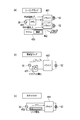
- the figure which shows the time chart corresponding to the flowchart of FIG. The figure which shows the operation mode allocated for every period of a switching pulse.
- the figure which shows the time chart corresponding to the operation mode of FIG. The figure which shows the operation mode of increase / decrease in switching frequency.
- the figure which shows the circuit structure of the switching current control circuit of this invention The figure which shows the determination method of the peak current value of the switching current control circuit of this invention.
- the figure which shows the time chart corresponding to the operation mode of FIG. A) The figure which shows the connection structure for evaluation using the switching current control circuit of this invention, and an input voltage characteristic,
- (b) Connection of circuit elements is basically the same as in FIG.
- FIG. 8 shows a circuit configuration in which a conventional switching current control circuit is connected to the drive circuit of the light emitting diode 52.
- the anode side of the light emitting diode 52 is connected to the DC power source 51, and the anode side of the light emitting diode 52 is connected to the inductor 53.
- a diode 54 is provided in parallel to the light emitting diode 52 and the inductor 53 connected in series.
- An FET (field effect transistor) 55 as a switching element is connected to the cathode side of the inductor 53 and the diode 54, and a current detection resistor 56 is connected in series to the FET 55.
- a switching current control circuit 70 for switching control of the FET 55 is provided.
- the switching current control circuit 70 includes a comparator 57 and an RS flip-flop 58.
- One end of the current detection resistor 56 is connected to a plus terminal of a comparator 57, and the other end of the current detection resistor 56 is connected to GND.
- the output of the comparator 57 is connected to the R terminal of the RS flip-flop 58, and the output of the RS flip-flop 58 is connected to the gate of the FET 55.
- the current flowing through the light emitting diode 52 is controlled using the switching current control circuit 70.
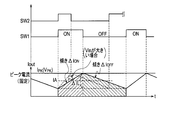
- the SW1 signal in the time chart of FIG. 9 is an output signal of the RS flip-flop 58 and an input signal to the gate of the FET 55.
- Iout in FIG. 9 is a current flowing through the light emitting diode 52 and the inductor 53. Further, during the ON period, the current Isen flowing through the current detection resistor 56 is the same current as Iout.
- Vpk indicates a peak voltage corresponding to the peak current (upper limit value) Ipk of the current Iout flowing through the light emitting diode 52.
- the output of the comparator 57 is at a low level, and a low level signal is input to the R terminal of the RS flip-flop 58. For this reason, when a high level pulse signal is input to the S terminal, the output of the RS flip-flop 58 becomes a high level signal, and the ON period continues.
- the FET 55 In the off period, the FET 55 is turned off, and no current flows through the FET 55 and the current detection resistor 56. However, the light emitting diode 52, the inductor 53, and the diode 54 form a closed circuit.
- the FET 55 When the FET 55 is turned off, the current that has been flowing through the inductor 53 until then is interrupted, and thus back electromotive force is generated in the inductor 53. Due to the counter electromotive force of the inductor 53, the diode 54 becomes conductive, and a current flows through the closed circuit of the light emitting diode 52, the inductor 53, and the diode 54. Since the back electromotive force of the inductor 53 gradually decreases, Iout also decreases linearly.
- the output current Iout changes due to changes in the voltage Vin of the DC power supply 51, the voltage drop Vout of the light emitting diode 52, and the inductance L of the inductor 53.
- the change in Iout increases the slopes ⁇ ION and ⁇ IOFF of the straight line portion of the triangular waveform of Iout.
- the peak current Ipk is fixed, and when Iout exceeds Ipk, the switching operation is turned off. When Iout is reduced beyond the lower limit current value, the switching operation is turned on. Becomes like SW2. Therefore, the current waveform of Iout changes greatly as shown by the broken line in FIG. 9, and the on-off period is shortened and the duty cycle is shortened. If the ON period becomes too short, a time during which the load current does not flow in the light emitting diode 53 occurs, and a so-called discontinuous mode (DCM) may occur.
- DCM discontinuous mode
- a switching current control circuit 100 is a switching current control circuit that controls a load current flowing through a predetermined device by a switching operation.
- a switching pulse supply circuit 90 that supplies a switching pulse for performing a switching operation
- a comparison circuit 91 that detects a load current in the ON period of the switching pulse as a detection current and compares it with a peak current value
- a calculation control circuit 3 for calculating a lower limit value of the detection current that gives a timing for switching from OFF to ON of the switching pulse, and the continuous mode when the lower limit value of the detection current calculated by the calculation control circuit 3 is 0 or more.
- the lower limit value of the detected current is a negative value, it is determined that the discontinuous mode is set.
- FIG. 1 shows a configuration example of a switching current control circuit 100 of the present invention.
- the same reference numerals as those in FIG. 8 denote the same circuit elements. Therefore, the light-emitting diode 52 is considered as an example of the load, and the drive circuit portion of the light-emitting diode 52 is similarly configured. That is, the DC power supply 51, the inductor 53, the diode 54, the FET 55, the current detection resistor 56, and the like are connected in the same manner as in FIG.
- the switching current control circuit 100 includes an analog circuit unit 100a and a digital circuit unit 100b.
- the analog circuit unit 100a includes a switching pulse supply circuit 90 and a comparison circuit 91.
- the comparison circuit 91 is configured by the comparator 1.
- the switching pulse supply circuit 90 includes a level shifter 9, a P-type MOS FET 10, an N-type MOS FET 11, and the like. The gate of the FET 10 and the gate of the FET 11 are connected, the source of the FET 10 and the drain of the FET 11 are connected, and the FET 10 and the FET 11 constitute an inverter.
- the digital circuit unit 100b includes an A / D converter 2, an arithmetic control circuit 3, an AD / DA offset setting unit 4, a D / A conversion circuit 5, a timing control circuit 6, a logic circuit 7, an RS flip-flop 8, and an initial value setting.
- the unit 12 includes a frequency setting unit (frequency setting circuit) 13, a comparator 14, and a frequency counter 15.
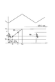
- FIG. 2 shows how the current flowing through the light emitting diode 52 is controlled by the switching current control circuit 100 of FIG.
- the upper part of FIG. 2 shows a change in load current flowing through the light emitting diode 52.
- the lower part shows a change in Isen flowing through the current detection resistor 56.
- the current Isen is the same as the current flowing through the light emitting diode.
- the FET 55 is turned off, so that the current Isen is zero.
- the graph SN shown in the figure shows such a state of the current Isen.
- the SN data is sampled at two time points t0 and t1 in the ON period.
- the SN data at t0 is y0
- the SN data at t1 is y1.
- Y1 in the figure is a value set by the initial value setting unit 12
- Y1 is a peak current value (upper limit current value) of the load current or detection current
- Y0 is a lower limit current value of the load current.
- the on period of the on / off period based on the initially set peak current value Y1 and the constant frequency is assumed to be Ton.
- t0 Ton ⁇ 1/4
- t1 Ton ⁇ 3/4.
- the current value at t0 of Isen is y0
- the current value at t1 of Isen is y1. From these data, the slope SL of the straight line portion of SN (Isen) is obtained.
- This slope SL is also an increase rate of the current Isen and an increase rate of the current flowing through the light emitting diode 52.
- the lower limit value Y0 ym ⁇ SL ⁇ Ton ⁇ (1/2).
- the lower limit value Y0 is 0 or more.
- the lower limit value Y0 can be set to 0 or more by increasing the switching frequency. In this way, it is possible to return to the pulse continuous mode.
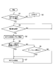
- FIG. 3 is a flowchart showing a normal operation when the switching frequency increasing / decreasing operation of the switching pulse is not considered.
- FIG. 4 shows a timing chart corresponding to the flowchart of FIG. In FIG. 4, the master clock MCLK is set to 5 MHz, for example. If SWCONVEN from the timing control circuit 6 is in the enable period, the switching pulse supply circuit 90 can be operated, so it is first determined whether or not SWCONVEN is in the enable period (step S1). If SWCONVEN is not in the enable period, the off mode is set (step S2), and the process returns to step S1 again.
- SWCONVEN is an enable period
- the process proceeds to the next step S3, where it is determined whether or not it is a current detection period (ON period). If it is not the current detection period, the process returns to step S3 again. If it is the current detection period, the process proceeds to step S4 to generate a SETCLK signal that is a blank period signal.
- the ISENS shown in FIG. 4 is the ISENS signal shown in FIG. 1 and corresponds to Vsens detected as a voltage by the comparison circuit 91. If the voltage Vsens is detected and the value of the current detection resistor 56 is known, the current Isen flowing through the current detection resistor 56 is known. Here, since it is easier to explain the operation by using the current signal, the ISENS signal is assumed to be the same current signal as the current Isen.
- the ISENS signal since the ISENS signal generates switching noise when the FET 55 is switched from OFF to ON, the ISENS signal is masked so as not to detect the current in this portion. This corresponds to the Blank Time of SETCLK and can be set to 400 ns, for example.
- the ISENS signal is compared with a preset peak current value Ipeak (step S5), and if it is larger than Ipeak, RSTCLK is generated (step S7), and the process returns to step S3.
- RSTCLK is generated and ISENS is larger than Ipeak
- the output IPEAKDET of the comparator 1 is at a high level.
- the output of the logic circuit 7 becomes a high level signal and is input to the R terminal of the RS flip-flop 8.
- the DC voltage level is adjusted by the level shifter 9 to become a high level signal.
- This high level signal is converted into a low level signal by an inverter circuit comprising FETs 10 and 11. That is, since VOUT becomes a low level signal, the FET 55 is turned off.
- step S6 it is determined whether the duty of the on / off period of the switching pulse is maximum. If the duty is not maximum, the process returns to step S5. If the duty is maximum, RSTCLK is generated (step S7), and the process returns to step S3. Also in this case, as in the case where the current ISENS is larger than the peak current value Ipeak, the FET 55 is turned off because VOUT becomes a low level signal.
- the A / D converter 2 includes two sample-holds and one AD converter.
- the A / D converter 2 outputs A / D converted values y0 and y1, which are input to the peak current calculation circuit 3.
- the D / A conversion circuit 5 is a decoder type D / A conversion circuit, and includes a DAC decoder 5a and an R-2R ladder type DA converter 5b.
- the AD / DA offset setting unit 4 stores the AD offset value of the A / D converter 2 measured in advance and the DA offset value of the D / A conversion circuit 5.
- the peak current calculation circuit 3 subtracts the AD offset value from the A / D conversion data and subtracts the DA offset value from the D / A conversion value. Is done.
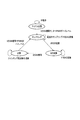
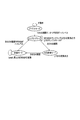
- FIG. 5 is a diagram showing the transition of the operation mode assigned for each cycle of the switching pulse when the switching frequency is increased or decreased in the switching current control circuit of the present invention.
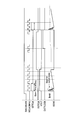
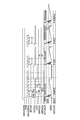
- FIG. 6 shows a time chart corresponding to the transition of the operation mode of FIG.
- FIG. 7 is a diagram showing transition of the operation mode when changing the switching frequency. 5 and 7, control signals are transmitted from a control unit (not shown).
- the initial state is an idle state and a non-operating state.
- SWCONVEN is in an enable period
- PWM is at a high level.
- the change of the period of the on-off period of the switching operation is enabled.
- the sampling mode is shifted to one cycle of the first first switching pulse.
- the sampling mode as shown in FIG. 2, it is desired to sample and hold the current value y0 at IS0 t0 and the current value y1 at t1, but the A / D converter 2 includes one AD converter. Therefore, A / D conversion cannot be performed while holding two values at a time.
- y0 is sampled and held by the sample hold in the A / D converter 2 at the first rising timing (1) of the SMPHLD1 signal as shown in FIG.
- the current value y0 is A / D converted and output at the rising timing (2).
- the y0 A / D conversion output is input to the arithmetic control circuit 3 as an ADOUT signal.
- the current value y1 is sampled and held by the sample hold of the A / D converter 2 at the second rising timing (3) of the SMPHLD1 signal.
- the cycle of the second switching pulse which is the on / off cycle of the next switching operation, is entered.
- the period of the second switching pulse is the A / D conversion mode.
- the current value y1 sampled and held in the sampling mode is A / D converted by the A / D converter 2 at the second rise timing (4) of the SMPHLD2 signal and output.
- the y1 A / D conversion output is input to the arithmetic control circuit 3 as an ADOUT signal.
- the process proceeds to the period of the third switching pulse, which is the on-off cycle of the next switching operation.
- the period of the third switching pulse is the calculation mode.
- the A / D converter 2 performs only A / D conversion of the current ISENS, and does not sample and hold the data of y0 and y1.
- the A / D conversion data of the current ISENS is output to the arithmetic control circuit 3 as an ADOUT signal.
- the arithmetic control circuit 3 determines whether it is a discontinuous mode or a continuous mode, as shown in FIG.
- the continuous mode (CCM) is determined when y1 ⁇ 3y0, and the discontinuous mode is determined when y1> 3y0. If it is determined that the mode is discontinuous, the frequency of the switching pulse is increased so that y1 ⁇ 3y0 and the continuous mode is restored.
- the value of the switching frequency to be changed is transmitted from the arithmetic control circuit 3 to the frequency setting circuit 13 and held, and the frequency value held in the frequency setting circuit 13 and the frequency counter 15
- the data is compared with the comparator 14 and when the frequency value is reached, the comparator 14 is caused to generate SETCLK.
- the frequency counter 15 is operated with a 10 MHz clock, for example. Since the SWON cycle and duty change according to the SETCLK signal, VOUT also changes in the same manner.
- the lower limit value Y0 when the switching frequency is increased, the lower limit value Y0 also increases. Therefore, when the increased lower limit value Y0 is satisfied, if 2y0> y1, it is determined that Y0 is sufficiently large and is set first. It is desirable to return to the switching frequency. Therefore, when the switching frequency is changed and y1> 2y0, the lower limit value Y0 is decreased to decrease the switching frequency and return to the initially set switching frequency.
- the switching frequency is decreased and the minimum duty cycle is released.
- the minimum duty cycle is 400 ns, which is the same as the Blank time for masking switching noise, and this on-time is a problem in operation.
- the lower limit value Y0 is decreased to decrease the switching frequency, and the on-time is lengthened to cancel the minimum duty cycle state.
- the value of the switching frequency to be changed is transmitted from the arithmetic control circuit 3 to the frequency setting circuit 13 and held, and the frequency value held in the frequency setting circuit 13 is compared with the data from the frequency counter 15.
- SETCLK is generated in the comparator 14.
- the peak current value (upper limit value) is normally fixed, but the peak current value can be changed.
- the peak current value is changed, the changed peak current value is output from the arithmetic control circuit 3 as a digital signal called IPEAKSET and supplied to the D / A conversion circuit 5.
- the D / A conversion circuit 5 D / A converts IPEAKSET and outputs it as an analog signal called IDAC, which becomes a new threshold voltage of the comparator 1.
- the output IPEAKDET of the comparator 1 becomes a high level signal when the current ISENS (voltage Vsens) exceeds the threshold voltage IDAC of the comparator 1, the output SWON through the subsequent logic circuit 7, RS flip-flop 8 and the like.
- the signal becomes a low level signal, and the DC voltage level is changed by the level shifter 9 to become a high level signal.
- This high level signal becomes a low level signal by the next inverter of the FETs 10 and 11, and the FET 55 is turned off.
- the load current during the ON period of the switching pulse is detected as the detection current and is output from the A / D conversion circuit 5 that converts it into digital data.
- a lower limit value of the detected current that gives a timing to switch the switching pulse from OFF to ON is calculated, and when the lower limit value of the detected current is 0 or more, it is determined that the continuous mode is set, When the lower limit value of the detection current is a negative value, it is determined that the discontinuous mode is set, and therefore, the determination can be made from the detection current without measuring the actual load current. it can.
- the switching current control circuit 100 itself is connected to the LED 52 via the switching element 55 and the inductor 53 so that the average current flowing through the LED 52 is controlled to be constant even when the frequency of the switching pulse is increased. it can. Thereby, power consumption can be suppressed.
- FIG. 8 shows a circuit configuration in which a conventional switching current control circuit is connected to the drive circuit of the light emitting diode 52.
- the anode side of the light emitting diode 52 is connected to the DC power source 51, and the cathode side of the light emitting diode 52 is connected to the inductor 53.
- a diode 54 is provided in parallel to the light emitting diode 52 and the inductor 53 connected in series.
- An FET (field effect transistor) 55 as a switching element is connected to the cathode side of the inductor 53 and the diode 54, and a current detection resistor 56 is connected in series to the FET 55.
- a switching current control circuit 70 for switching control of the FET 55 is provided.
- the switching current control circuit 70 includes a comparator (comparator) 57 and an RS flip-flop 58.
- One end of the current detection resistor 56 is connected to the plus terminal of the comparator 57, and the other end of the current detection resistor 56 is connected to GND.
- the output of the comparator 57 is connected to the R terminal of the RS flip-flop 58, and the output of the RS flip-flop 58 is connected to the gate of the FET 55.
- the current flowing through the light emitting diode 52 is controlled using the switching current control circuit 70.
- the SW signal in the time chart of FIG. 13 is an output signal of the RS flip-flop 58 and an input signal to the gate of the FET 55.
- Iout in FIG. 9 is a current flowing through the light emitting diode 52 and the inductor 53. Further, during the ON period, the current Isen flowing through the current detection resistor 56 is the same current as Iout.
- Vpk indicates a peak voltage corresponding to the peak current (upper limit value) Ipk of the current Iout flowing through the light emitting diode 52.
- the output of the comparator 57 is at a low level, and a low level signal is input to the R terminal of the RS flip-flop 58. For this reason, when a high level pulse signal is input to the S terminal, the output of the RS flip-flop 58 becomes a high level signal, and the ON period continues.
- the FET 55 In the off period, the FET 55 is turned off, and no current flows through the FET 55 and the current detection resistor 56. However, the light emitting diode 52, the inductor 53, and the diode 54 form a closed circuit.
- the FET 55 When the FET 55 is turned off, the current that has been flowing through the inductor 53 until then is interrupted, and thus back electromotive force is generated in the inductor 53. Due to the counter electromotive force of the inductor 53, the diode 54 becomes conductive, and a current flows through the closed circuit of the light emitting diode 52, the inductor 53, and the diode 54. Since the back electromotive force of the inductor 53 gradually decreases, Iout also decreases linearly.
- Iout has a triangular wave shape, but the current flowing through the light-emitting diode 52 is obtained by an integral value of Iout. Thereby, the average value of the current flowing through the light emitting diode 52 is calculated.
- the output current Iout changes due to changes in the voltage Vin of the DC power supply 51, the voltage drop Vout of the light emitting diode 52, and the inductance L of the inductor 53.
- the change in Iout increases the slopes ⁇ ION and ⁇ IOFF of the straight line portion of the triangular waveform of Iout.
- a switching current control circuit 100 is a switching current control circuit that controls a load current flowing through a predetermined device by a switching operation.
- a switching pulse supply circuit 90 that supplies a switching pulse for performing a switching operation
- a comparison circuit 91 that detects a load current in the ON period of the switching pulse as a detection current and compares it with a peak current value
- a switching The linear increase rate of the detection current during the pulse ON period is calculated, and the maximum current value is calculated using the increase rate when the detection current is assumed to increase until the end of the ON period of the switching operation.
- a peak current calculation circuit 3 having a peak current value as a value. When the detected current exceeds the peak current value calculated by the peak current calculation circuit 3, the switching pulse is turned off by the output signal of the comparison circuit 91. Is.
- FIG. 10 shows a configuration example of the switching current control circuit 100 of the present invention.
- the same reference numerals as those in FIG. 8 indicate the same circuit elements. Therefore, the light emitting diode 52 of FIG. 8 is considered as an example of the load, and the drive circuit portion of the light emitting diode 52 is similarly configured. That is, the DC power supply 51, the inductor 53, the diode 54, the FET 55, the current detection resistor 56, and the like are connected in the same manner as in FIG.
- the switching current control circuit 100 includes an analog circuit unit 100a and a digital circuit unit 100b.
- the analog circuit unit 100a includes a switching pulse supply circuit 90 and a comparison circuit 91.
- the comparison circuit 91 is configured by the comparator 1.
- the switching pulse supply circuit 90 includes a level shifter 9, a P-type MOS FET 10, an N-type MOS FET 11, and the like. The gate of the FET 10 and the gate of the FET 11 are connected, the source of the FET 10 and the drain of the FET 11 are connected, and the FET 10 and the FET 11 constitute an inverter.
- the digital circuit unit 100b includes an A / D converter 2, a peak current calculation circuit 3, an AD / DA offset setting unit 4, a D / A conversion circuit 5, a timing control circuit 6, a logic circuit 7, an RS flip-flop 8, an initial value
- the setting unit 12 is configured.
- FIG. 11 shows how the current flowing through the light emitting diode 52 is controlled by the switching current control circuit 100 of FIG.
- the upper part of FIG. 11 shows changes in the current flowing through the light emitting diode 52.
- the lower part shows a change in Isen flowing through the current detection resistor 56.
- the current Isen is the same as the current flowing through the light emitting diode.
- the FET 55 is turned off, so that the current Isen is zero.
- the SN data is sampled at two time points t0 and t1 in the ON period.
- the SN data at t0 is y0
- the SN data at t1 is y1.
- Y1 and Y0 are values set by the initial value setting unit 12
- Y1 is a peak current value (upper limit current value) of the load current or detected current
- Y0 is a lower limit current of the load current or detected current.
- the initially set peak current value is Y1
- the lower limit value is Y0
- the on period of the on / off period based on these Y1 and Y0 is Ton.
- the current Isen at the first time and the current flowing through the light emitting diode 52 are indicated by broken lines, and the off period at that time is off 2.
- the lower limit value Y0 is fixed without being changed.
- the new upper limit value Y12 is calculated by the same algorithm as described above.
- the average value of the upper limit value Y11 and the lower limit value Y0 is AVE1.
- y2 and y3 are data sampled at two points during the ON period. The sampling at these two points is performed at the time point 1/4 of Ton and the time point 3/4 of Ton.
- AVE1 (y2 + y3) / 2
- Y12 AVE1 + ((y3 ⁇ y2) / 2) ⁇ (Ton / 2).
- FIG. 3 is a flowchart showing a normal operation when a change in the slope SL of the straight line of the current Isen is not taken into consideration.
- the master clock MCLK is set to 5 MHz, for example. If SWCONVEN from the timing control circuit 6 is in the enable period, the switching pulse supply circuit 90 can be operated, so it is first determined whether or not SWCONVEN is in the enable period (step S1). If SWCONVEN is not in the enable period, the off mode is set (S step 2), and the process returns to step S1 again.
- SWCONVEN is an enable period
- the process proceeds to the next step S3, where it is determined whether or not it is a current detection period (ON period). If it is not the current detection period, the process returns to step S3 again. If it is the current detection period, the process proceeds to step S4 to generate a SETCLK signal that is a blank period signal.
- ISENS shown in FIG. 4 is the Isens signal shown in FIG. 10 and corresponds to Vsens detected as a voltage by the comparison circuit 91. If the voltage Vsens is detected and the value of the current detection resistor 56 is known, the current Isen flowing through the current detection resistor 56 is known.
- the ISENS signal is assumed to be the same current signal as the current Isen.
- the ISENS signal since the ISENS signal generates switching noise when the FET 55 is switched from OFF to ON, the ISENS signal is masked so as not to detect the current in this portion. This corresponds to the Blank Time of SETCLK and can be set to 400 ns, for example.
- the ISENS signal is compared with a preset peak current value Ipeak (step S5), and if it is larger than Ipeak, RSTCLK is generated (step S7), and the process returns to step S3.
- RSTCLK is generated and ISENS is larger than Ipeak
- the output IPEAKDET of the comparator 1 is at a high level.
- the output of the logic circuit 7 becomes a high level signal and is input to the R terminal of the RS flip-flop 8.
- the DC voltage level is adjusted by the level shifter 9 to become a high level signal.
- This high level signal is converted into a low level signal by an inverter circuit comprising FETs 10 and 11. That is, since VOUT becomes a low level signal, the FET 55 is turned off.
- step S6 it is determined whether the duty of the on / off period of the switching pulse is maximum. If the duty is not maximum, the process returns to step S5. If the duty is maximum, RSTCLK is generated (step S7), and the process returns to step S3. Also in this case, as in the case where the current ISENS is larger than the peak current value Ipeak, the FET 55 is turned off because VOUT becomes a low level signal.
- the A / D converter 2 includes two sample-holds and one AD converter.
- the A / D converter 2 outputs A / D converted values y0 and y1, which are input to the peak current calculation circuit 3.
- the D / A conversion circuit 5 is a decoder type D / A conversion circuit, and includes a DAC decoder 5a and an R-2R ladder type DA converter 5b.
- the AD / DA offset setting unit 4 stores the AD offset value of the A / D converter 2 measured in advance and the DA offset value of the D / A conversion circuit 5.
- the peak current calculation circuit 3 subtracts the AD offset value from the A / D conversion data and subtracts the DA offset value from the D / A conversion value. Is done.
- FIG. 12 is a diagram showing the transition of the operation mode assigned for each cycle of the switching pulse when the peak current value is changed in the switching current control circuit of the present invention.
- FIG. 13 is a time chart corresponding to the transition of the operation mode of FIG.
- the initial state is an idle state and a non-operating state.
- SWCONVEN is in an enable period
- PWM is at a high level.
- the sampling mode is shifted to one cycle of the first first switching pulse.
- the sampling mode as shown in FIG. 11, it is desired to sample and hold the current value y0 at IS0 t0 and the current value y1 at t1, but the A / D converter 2 includes one AD converter. Therefore, A / D conversion cannot be performed while holding two values at a time.
- y0 is sampled and held by the sample hold in the A / D converter 2 at the first rising timing (1) of the SMPHLD1 signal, as shown in FIG.
- the current value y0 is A / D converted and output at the rising timing (2).
- the y0 A / D conversion output is input to the peak current calculation circuit 3 as an ADOUT signal.
- the current value y1 is sampled and held by the sample hold of the A / D converter 2 at the second rising timing (3) of the SMPHLD1 signal.
- the cycle of the second switching pulse which is the on / off cycle of the next switching operation, is entered.
- the period of the second switching pulse is the A / D conversion mode.
- the current value y1 sampled and held in the sampling mode is A / D converted by the A / D converter 2 at the second rise timing (4) of the SMPHLD2 signal and output.
- the y1 A / D conversion output is input to the peak current calculation circuit 3 as an ADOUT signal.
- the process proceeds to the period of the third switching pulse, which is the on-off cycle of the next switching operation.
- the period of the third switching pulse is the calculation mode.
- the A / D converter 2 performs only A / D conversion of the current ISENS, and does not sample and hold the data of y0 and y1.
- the A / D conversion data of the current ISENS is output to the peak current calculation circuit 3 as an ADOUT signal.
- the peak current calculation circuit 3 calculates a new peak current value Y11 by using the AD offset value, the DA offset value, and the like stored in the setting unit 4.
- the new peak current value Y11 is output from the peak current calculation circuit 3 as a digital signal called IPEAKSET and supplied to the D / A conversion circuit 5.
- the D / A conversion circuit 5 D / A converts IPEAKSET and outputs it as an analog signal called IDAC, which becomes a new threshold voltage of the comparator 1.
- the output IPEAKDET of the comparator 1 becomes a high level signal when the current ISENS (voltage Vsens) exceeds the new threshold voltage IDAC of the comparator 1, the output through the subsequent logic circuit 7 and RS flip-flop 8 etc.
- the SWON signal becomes a low level signal, and the DC voltage level is changed by the level shifter 9 to become a high level signal.
- This high level signal becomes a low level signal by the next inverter of the FETs 10 and 11, and the FET 55 is turned off. In other words, with reference to the signal of FIG. 13, the FET 55 is turned off at the timing (5) when the current ISENS exceeds the new peak current value Ipeak. In this way, the sampling mode, A / D conversion mode, and calculation mode of FIG. 12 are repeated.
- the peak current value set by the switching current control circuit is changed each time according to the linear increase rate (increase rate) of Isen that is the detected current.
- the maximum current value when reaching the end point of the ON period of the initially set switching period while maintaining the linear increase rate of the detection current Isen is changed to the new peak current. Value.
- the on-off cycle of the switching operation changes, but the on period of the switching operation does not change from the initial setting and is in a fixed state. Since the operation is performed in this way, the integrated value of the current flowing through the light emitting diode can be maintained at a substantially constant value even if the increase rate of the detected current changes, so that the average current value flowing through the load is Does not fluctuate.
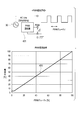
- the switching current control circuit 100 of the present embodiment is arranged on the evaluation substrate, and the variable DC power source VIN for input voltage and the light emitting diode 52 are connected. That is, the components of the DC power supply 51, the light emitting diode 52, the inductor 53, the FET 55, and the current detection resistor 56 in FIG. 8 are used as they are, and a circuit configuration using the variable DC power supply VIN instead of the DC power supply 51 is adopted.
- the light emitting diode 52 six 1W LEDs connected in series were used as the light emitting diode 52.
- the current IL flowing through the light emitting diode 52 was measured with the ammeter 60 while changing the input voltage VIN.
- the result is shown in FIG.
- the horizontal axis indicates VIN (V)
- the vertical axis indicates the current IL (mA).
- the current IL hardly fluctuated with respect to the change of the input voltage VIN, and a preferable result was obtained.
- the area A is based on the maximum duty cycle (50%) which is a limit, and is not a problem.
- the circuit elements are basically connected in the same manner as FIG. 14B, but the power source is changed from the variable DC power source VIN to a 100V AC power source, and this AC power source is converted to a DC voltage. Used as input voltage.
- the light-emitting diode 52 was a 15-W LED connected in series.
- the measurement result is shown in FIG.
- the horizontal axis indicates the DC input voltage VL (V)
- the vertical axis indicates the current IL (mA) flowing through the light emitting diode 52. Even when the input voltage VL was changed, there was almost no change in the current IL, and a favorable result was obtained.
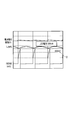
- FIG. 16 shows the results of measuring the power supply voltage fluctuation, the current IL flowing through the LED, and the voltage ISENSE input to the comparator 1 in the configuration of FIG. 14 or FIG.
- one scale indicates 5 V
- voltage ISENSE one scale indicates 200 mV.
- feedback is performed so that the average voltage ISENS is 500 mV (line D in the figure).
- the average current of IL is maintained at 335 mA.
- FIG. 17 shows the result of measuring the current IL flowing through the light emitting diode by changing the input voltage using the switching current control circuit of the present invention as shown in FIG. 14 or 15 (input voltage characteristic X). 14 and FIG. 15 using a conventional switching current control circuit of another company's product, and similarly, the result of measuring the current IL flowing through the light emitting diode by changing the input voltage (input voltage characteristic Y , Z).
- the current detection resistor 56 was 1 ⁇ .
- the vertical axis represents current IL (mA), and the horizontal axis represents input voltage (V).
- the switching current control circuit of the present embodiment As can be seen from the input voltage characteristic X by the switching current control circuit of the present embodiment, it can be seen that a constant current flows through the light emitting diode even if the input voltage changes.
- especially the Z or the like is not preferable because the current flowing through the light emitting diode decreases with the change of the input voltage.
- the power factor can be improved and flicker can be prevented. Therefore, it can be applied to a PFC (power factor correction) circuit, a circuit without an electrolytic capacitor, and the like.
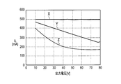
- FIG. 18 shows the result of measuring the relationship (output voltage characteristics) between the current IL flowing through the light emitting diode and the output voltage of the light emitting diode in the measurement performed in FIG.
- the vertical axis represents current IL (mA)
- the horizontal axis represents output voltage (V).
- the switching current control circuit 100 shows that the current IL is not affected by the magnitude of the voltage drop of the light emitting diode. Therefore, the switching current control circuit 100 of the present embodiment can also be applied to a case where a plurality of various LEDs are used and connected in series.
- the average current flowing through the light emitting diode changes in the voltage Vin of the DC power supply 51, the voltage drop of the light emitting diode 52, and the inductance L of the inductor 53. Even if there is, as described above, the peak current value is changed according to the increasing rate of the detection current Isen (ISENSE), and the ON period of the switching period is not changed. For this reason, the average current flowing through the light-emitting diode is not affected by elements other than the current detection resistor 56 serving as an external resistor. Therefore, the average current value flowing through the light-emitting diode is appropriately set by changing only the external resistor. can do.
- the linear increase rate of the detection current during the ON period of the switching pulse is calculated, and the maximum current value when the detection current is assumed to increase until the end of the ON period of the switching operation is calculated using the increase rate.
- the maximum current value is replaced with a peak current value.
- the peak current value input to the comparison circuit changes according to the linear increase rate of the detection current, and the peak current value increases as the detection current linear increase rate increases. Since the peak current value also decreases as the increase rate decreases, the peak current value increases even if, for example, the linear increase rate of the detection current increases, the on-off cycle is shortened, and the on-period is shortened. Since the maximum value of the load current increases, the average current can be kept constant.
- PWM pulse width modulation
- triac dimming phase dimming
- linear dimming linear dimming
- PWM dimming is a method of adjusting the brightness by controlling the lighting time and extinguishing time of the LED.
- the brightness is controlled by adjusting the duty ratio (ratio between on time and off time) of the PWM signal output from the PWM dimmer 401.
- curves a and b indicate the relationship between the PWM duty and current ratio in the case of DC output and burst output.
- a voltage dimming method for dimming by changing a voltage (or current) supplied to the LED and a burst dimming method for intermittently lighting the lamp by a PWM pulse.
- the curve a indicates the voltage dimming method
- the curve b indicates the burst dimming method.
- the brightness is adjusted by controlling the timing (phase angle) for giving a trigger to the TRIAC included in the TRIAC dimmer 32.
- TRIAC dimming is a method mainly used to adjust the brightness of lighting fixtures installed in ordinary houses. This is a mechanism to adjust the brightness by cutting out a part of the input alternating current using a triac with a structure in which thyristors are combined face to face (in reverse parallel).
- the diode when a trigger is applied to the triac in the middle of the AC waveform, the diode changes to a conductive state (ON state), and this state continues until the AC waveform reaches 0V.
- ⁇ Adjust the brightness by controlling the timing to give the trigger, that is, the angle at which the AC waveform is cut out. If the timing to give a trigger is early (small angle), it becomes bright, and if the timing is late (large angle), it becomes dark.
- This triac dimming is characterized by high consistency with incandescent bulbs whose brightness is determined by the effective value of input power.
- the curve c indicates the DC output and the curve d indicates the burst output.
- area E1 indicates a range suitable for dimming according to the sensitivity of the human eye.
- the linear dimming is a method of performing dimming by changing a DC voltage by a variable resistor 402 such as a volume resistor or a slide resistor.
- the curve e indicates the DC output and the curve f indicates the burst output.
- area E2 indicates a range suitable for dimming according to the sensitivity of the human eye.
- the triac dimmer 32 needs to keep a holding current flowing when the triac is turned on, and the triac is turned off when it falls below the holding current.
- the triac is turned off when the holding current for the triac included in the triac dimmer falls below the threshold due to the discharge of the smoothing capacitor or the like, and when the triac is turned on again, the triac is turned off again for the same reason.
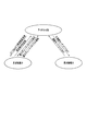
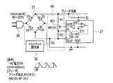
- a bleeder resistor R1 connected to the output side of the triac dimmer 32 and a bleeder controller 21 that controls the current flowing through the bleeder resistor R1 are provided. .
- the LED dimming system S according to the third embodiment is an LED dimming system that includes the switching current control circuit 100 according to the first or second embodiment and performs dimming of the LED 52, and is an AC power source. 30, a bridge-type full-wave rectifier circuit 31 connected to one end of the AC power supply 30, a triac dimmer 32 connected to the other end of the AC power supply 30, and a bleeder resistor R 1 connected to the output side of the triac dimmer 32. And a bleeder control unit 21 that controls the current flowing through the bleeder resistor R1.
- the bleeder control unit 21 performs control so as to supply a predetermined holding current for holding the ON state to the triac dimmer 32 via the bleeder resistor R1.
- the LED dimming system S is roughly divided into a control unit 20 that controls the entire system, and LEDs that are turned on by the control of the control unit 20 (in the example shown in FIG. 22, a plurality of LEDs are connected in series). 52, a dimmer 150 that performs triac dimming of the LED 52, a bleeder circuit 40 that supplies a holding current to the triac dimmer 32 included in the dimmer 150, and other circuit components.
- the control unit 20 includes the switching current control circuit 100 according to the first or second embodiment, the bleeder control unit 21 that controls the bleeder circuit 40, and any of triac dimming, PWM dimming, and linear dimming.
- a dimming interface unit 22 to be selected, a power supply unit 23 that supplies power to the entire system, and a dimming control unit 24 that performs dimming control are provided.
- FIG. 22 shows a schematic configuration of the switching current control circuit 100. Since the detailed configuration of the switching current control circuit 100 has been described in the description of the first or second embodiment, the same members are denoted by the same reference numerals and the description thereof is omitted.
- the OSC 201 is an oscillator that generates a signal of 20 to 30 kHz.
- the bleeder control unit 21 is connected to a bleeder control logic circuit 213 that outputs a logical operation result to a NOT circuit 212 connected to a gate electrode of a switching element TR2 described later, and a control resistor R2 and a monitor resistor R3 described later.
- An operational amplifier 210 that inputs an amplified signal to the bleeder control logic circuit 213, and an FET 211 that has a drain electrode connected to the control resistor R2 and a gate electrode connected to the bleeder control logic circuit 213.
- the dimming interface unit 22 includes an operational amplifier 221 connected to the triac input side, a NOT circuit 222 connected to the PWM input side, and a linear input terminal LD.
- the operational amplifier 221, the NOT circuit 222, and the linear output terminal are regulated. It is connected to the light control unit 24.
- the dimming interface unit 22 includes a first dimming mode for performing phase dimming using the triac dimmer 32, a second dimming mode for performing pulse width modulation dimming, and linear using a variable resistor. It functions as switching means for switching to the third dimming mode for performing dimming.
- the power supply unit 23 includes a protection circuit 231 and a power supply unit 232 that supplies power of 12 V and 3.3 V.
- the protection circuit 231 has functions such as LED open / short protection, power supply voltage abnormality protection, temperature abnormality protection, and detection terminal open / short protection.
- the dimming control unit 24 includes a dimming control logic circuit 242 that controls triac dimming, PWM dimming, and linear dimming, and a soft start timer 241 that gently turns on the LED 52.
- the dimmer 150 is connected to the AC power source (AC power source) 30, a bridge-type full-wave rectifier circuit 31 including a bridge diode connected to one end side of the AC power source 30, and the other end side of the AC power source 30. And a bleeder resistor R1 connected to the output side of the triac dimmer 32.
- a control resistor R2 and a monitor resistor R3, which will be described later, are connected to the anodes of the diodes D2, D3 of the bridge diode constituting the bridge-type full-wave rectifier circuit 31.
- the cathode of the bridge diode of the diode D1, D4 constituting the bridge type full-wave rectifying circuit 31 is connected to LED52 through the diode D IN.
- the bleeder circuit 40 includes a bleeder resistor R1 connected to the drain electrode of the FET 401 as a switching element, a control resistor R2 connected to the source electrode of the FET 401, and a monitor resistor R3 connected to the control resistor R2 via the node N1. And.
- control resistor R2 and the monitor resistor R3 are connected to the operational amplifier 210 of the bleeder control unit 21 via the node N2.
- the bleeder resistor R1 is a resistor that supplies a holding current to the triac of the triac dimmer 32 through the bridge-type full-wave rectifier circuit 31.
- the resistance value is 1 K ⁇ .
- the source electrode of the FET 401 and the control resistor R2 are connected to the drain electrode of the FET 211 provided in the bleeder control unit 21 via the node N3.
- the resistance value of the control resistor R2 is 330 ⁇ .
- the monitor resistor R3 is a resistor that monitors the holding current supplied to the triac of the triac dimmer 32.
- the resistance value of the monitor resistor R3 is 2 ⁇ .
- the triac input terminal VHV of the dimming interface unit 22 is connected to boost resistors R VHV1 and R VHV2 via a node N10.
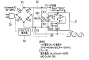
- the bleeder control unit 21 controls the bleeder current supplied from the bleeder circuit 40 by turning on / off the FET 401 according to the value of the current flowing through the monitor resistor R3, and prevents the triac dimmer 32 from malfunctioning. Thereby, the flicker of LED52 is suppressed.
- the AC voltage of the AC power supply (AC power supply) 30 is ON and the voltage VHV ⁇ 400 mA.
- both the FET 211 and the FET 401 are turned on, and control is performed so that a sufficient current is supplied to the triac of the triac dimmer 32 via the bleeder resistor R1 and the control resistor R2.
- the condition is that the voltage of the AC power supply (AC power supply) 30 is ON and the AC current is small, for example, the voltage VHV ⁇ 400 mA, ISUP> ⁇ 100 mA.
- the FET 211 is OFF and the FET 401 is ON.
- the holding current I HLD can be set to 20 to 50 mA by changing the resistance value of the control resistor R2.
- the triac of the triac dimmer 32 can be kept on, and flickering of the LED 52 is prevented.
- the voltage of the AC power supply (AC power supply) 30 is ON and the AC current is large, for example, the conditions of voltage VHV ⁇ 400 mA and ISUP ⁇ ⁇ 100 mA. In this case, both the FET 211 and the FET 401 are turned off.
- the triac can be kept in the on state, and flickering of the LED 52 is prevented.
- Lighting devices using the LED 52 include a ceiling lamp (ceiling light type LED lighting device) disposed on the ceiling of a living room, a light bulb type lamp (light bulb type LED lighting device) and a spotlight used in place of an incandescent bulb. Type LED lighting equipment.
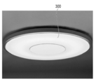
- FIG. 26 illustrates a ceiling light type LED lighting device 300.
- the ceiling light type LED lighting apparatus 300 includes, for example, power consumption (41 W), light color (white daylight + bulb color), fixture luminous flux (3220 lm), applicable tatami mat number (8 tatami mats), width (500 mm), depth (500 mm) , Height (39 mm), weight (2.8 kg).
- the ceiling light type LED lighting device 300 can use a PWM dimming method as shown in FIG. 29 (a), for example.
- a power factor correction (PFC) circuit 465 As shown in FIG. 29 (a), for example, a power factor correction (PFC) circuit 465, drivers 461 and 462, and a microcomputer 450 that controls devices by wireless operation are provided.
- PFC power factor correction
- the dimming interface unit 22 switches to the second dimming mode for performing pulse width modulation dimming. Controlled.
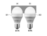
- FIG. 27 exemplifies bulb-type LED lighting devices 301 and 302.
- the light bulb type LED lighting device 301 in FIG. 27 (a) emits light of daylight, and the light bulb type LED lighting device 301 in FIG. 27 (b) emits light of a light bulb color.
- Both the bulb-type LED lighting devices 301 and 302 have, for example, power consumption (6 W), luminous flux (390 lm), life (40000 hours), and base standard (E26).
- the dimming interface unit 22 When the LED dimming system S according to the present embodiment is applied to the bulb-type LED lighting devices 301 and 302, the dimming interface unit 22 performs phase dimming using the triac dimmer 32. It is controlled by switching to the 1 dimming mode. That is, as shown schematically in FIG. 29B, triac dimming is performed using a driver 463 to which the LED dimming system S is applied.
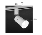
- FIG. 28 illustrates a spotlight type LED lighting device 303.
- the spotlight type LED lighting device 303 is movably attached to the rail 304 via an attachment 305.
- the spotlight type LED lighting device 303 is, for example, power consumption (4 W), luminous flux (256 lm), and base standard (E17).
- the dimming interface unit 22 When the LED dimming system S according to this embodiment is applied to the spotlight type LED lighting device 303, the dimming interface unit 22 performs the third dimming that performs linear dimming using a variable resistor. It is controlled by switching to the mode.
- dimming control is performed using a slide resistor 452 and a driver 464.
- the switching current control circuit of the present invention can be applied to a device that performs constant current driving, such as an LED, or an integrated circuit for driver of a device that is driven by constant current.
- the LED dimming system of the present invention can be applied to a light bulb type LED lighting device or a ceiling light type LED lighting device.
Landscapes
- Circuit Arrangement For Electric Light Sources In General (AREA)
- Control Of Electrical Variables (AREA)
Abstract
Description
(比較例)
第1の実施の形態に係るスイッチング電流制御回路100について説明するに先立って、比較例に係るスイッチング電流制御回路について、図8および図9を参照して説明する。
図1に示すように、第1の実施の形態に係るスイッチング電流制御回路100は、所定の装置に流れる負荷電流をスイッチング動作により制御するスイッチング電流制御回路である。
よって、y1≦3y0のときに、連続モード(CCM)又は臨界モード(BCM)となる。反対に、y1>3y0の場合は、不連続モードとなる。
(比較例)
第2の実施の形態に係るスイッチング電流制御回路100について説明するに先立って、比較例に係るスイッチング電流制御回路について、前出の図8および図9を参照して説明する。
図10に示すように、第2の実施の形態に係るスイッチング電流制御回路100は、所定の装置に流れる負荷電流をスイッチング動作により制御するスイッチング電流制御回路である。
Y12=AVE1+((y3-y2)/2)×(Ton/2)となる。
図19から図29を参照して第3の実施の形態に係るLED調光システムSおよびLED照明機器について説明する。
まず、図19から図21を参照して、LEDの調光方式について簡単に説明する。
第3の実施の形態に係るLED調光システムSは、第1または第2の実施の形態に係るスイッチング電流制御回路100を備え、LED52の調光を行うLED調光システムであって、交流電源30の一端側に接続されるブリッジ形全波整流回路31と、交流電源30の他端側に接続されるトライアック調光器32と、トライアック調光器32の出力側に接続されるブリーダ抵抗R1と、ブリーダ抵抗R1に流れる電流を制御するブリーダ制御部21とを備える。
図23から図25を参照して、ブリーダ制御部21およびブリーダ回路40で行われるブリーダ制御について説明する。
LED52を用いた照明機器としては、リビングルーム等の天井に配置されるシーリンランプ(シーリングライト型LED照明機器)、白熱球に代えて使用される電球型ランプ(電球型LED照明機器)やスポットライト型LED照明機器などがある。
上記のように、実施の形態によって記載したが、この開示の一部をなす論述および図面は例示的なものであり、この発明を限定するものであると理解すべきではない。この開示から当業者には様々な代替実施の形態、実施例および運用技術が明らかとなろう。
2…A/D変換器
3…演算制御回路
4…AD/DAオフセット設定部
5…D/A変換回路
5a…DACデコーダ
5b…R-2R型DA変換器
6…タイミング制御回路
7…論理回路
8、58…RSフリップフロップ
9…レベルシフト器
10、11、55、211、401…FET
12…初期値設定部
13…周波数設定部(周波数設定回路)
15…周波数カウンタ
20…制御部
21…ブリーダ制御部
22…調光インターフェイス部
23…電源供給部
24…調光制御部
30…交流電源
31…ブリッジ形全波整流回路
32…トライアック調光器
40…ブリーダ回路
51…直流電源
52、53…発光ダイオード
54…ダイオード
56…電流検出抵抗
60…電流計
70、100…スイッチング電流制御回路
90…スイッチングパルス供給回路
91…比較回路
100a…アナログ回路部
100b…デジタル回路部
150…調光部
201…OSC
210、221…オペアンプ
212、222…NOT回路
213…ブリーダ制御論理回路
231…保護回路
232…電源部
241…ソフトスタートタイマ
242…調光制御論理回路
300…シーリングライト型LED照明機器
301…電球型LED照明機器
303…スポットライト型LED照明機器
304…レール
305…取付け具
401…PWM調光器
402…可変抵抗
450…マイクロコンピュータ
452…スライド抵抗
461、463、464…ドライバ
465…PFC回路
Claims (27)
- 所定の装置に流れる負荷電流をスイッチング動作により制御するスイッチング電流制御回路であって、
前記スイッチング動作を行うためのスイッチングパルスを供給するスイッチングパルス供給回路と、
前記スイッチングパルスのオン期間における負荷電流を検出電流として検出してピーク電流値と比較する比較回路と、
前記スイッチングパルスのオン期間における負荷電流を検出電流として検出してデジタルデータに変換するA/D変換回路と、
前記A/D変換回路から出力される検出電流のデータに基づいて、前記スイッチングパルスのオフからオンに切り替えるタイミングを与える検出電流の下限値を算出する演算制御回路と
を備え、
前記演算制御回路の算出した前記検出電流の下限値が0以上である場合に連続モードであると判定し、前記検出電流の下限値が負の値の場合は不連続モードであると判定することを特徴とするスイッチング電流制御回路。 - 前記検出電流の下限値により不連続モードであると判定された場合は、前記スイッチングパルスの周波数を上げることにより、前記検出電流の下限値が0以上となるようにすることを特徴とする請求項1に記載のスイッチング電流制御回路。
- 前記スイッチングパルスの周波数を上げることにより、前記検出電流の下限値が0以上なり、さらに所定の値を超えたときに、前記スイッチングパルスの周波数を最初に設定されていた周波数に戻すことを特徴とする請求項2に記載のスイッチング電流制御回路。
- 前記検出電流の下限値により連続モードと判定され、かつ前記スイッチングパルスのオン期間が、前記スイッチングパルスのオンからオフに切り替る際に起きるスイッチングノイズ発生期間以下の長さの場合には、前記スイッチングパルスの周波数を下げることを特徴とする請求項1に記載のスイッチング電流制御回路。
- 前記A/D変換回路は、前記スイッチングパルスのオン期間における検出電流を逐次A/D変換するか、または検出電流の2点における電流値をA/D変換することを特徴とする請求項1~4のいずれか1項に記載のスイッチング電流制御回路。
- 前記A/D変換回路は、2つのサンプルホールド回路と1つのA/Dコンバータとで構成されていることを特徴とする請求項5に記載のスイッチング電流制御回路。
- 前記A/D変換回路は、前記スイッチングパルスの3周期分の1周期毎に動作モードが割り当てられており、第1の周期では、前記A/D変換回路によって前記検出電流の2点における電流値のうち一方の値をA/D変換出力し、他方の値をサンプルホールドすることを特徴とする請求項6に記載のスイッチング電流制御回路。
- 前記スイッチングパルスの第2の周期では、前記第1の周期においてサンプルホールドしていた電流値を、前記A/D変換回路によってA/D変換出力することを特徴とする請求項7に記載のスイッチング電流制御回路。
- 前記スイッチングパルスの第3の周期では、スイッチングパルスのオン期間における検出電流を逐次A/D変換することを特徴とする請求項7または請求項8のいずれかに記載のスイッチング電流制御回路。
- スイッチング電流制御回路自身は、スイッチング素子およびインダクタを介してLEDに接続され、
前記スイッチングパルスの周波数を上げた場合にも、前記LEDに流れる平均電流が一定となるように制御することを特徴とする請求項1~9のいずれか1項に記載のスイッチング電流制御回路。 - 所定の装置に流れる負荷電流をスイッチング動作により制御するスイッチング電流制御回路であって、
前記スイッチング動作を行うためのスイッチングパルスを供給するスイッチングパルス供給回路と、
前記スイッチングパルスのオン期間における負荷電流を検出電流として検出してピーク電流値と比較する比較回路と、
前記スイッチングパルスのオン期間における検出電流の直線的な増加率を算出し、該増加率を用いてスイッチング動作のオン期間終了まで検出電流が増加したと仮定した場合の最大電流値を算出して該最大電流値を前記ピーク電流値とするピーク電流算出回路と
を備え、
前記検出電流が前記ピーク電流算出回路により算出されたピーク電流値を越えたときに前記比較回路の出力信号により前記スイッチングパルスがオフ期間となることを特徴とするスイッチング電流制御回路。 - 前記検出電流の直線的な増加率は、前記スイッチングパルスのオン期間における検出電流の2点の電流値を検出し、この2点間の直線の傾きを求めることにより算出されることを特徴とする請求項11に記載のスイッチング電流制御回路。
- 前記スイッチングパルスをオフ期間からオン期間に切り替えるために、前記負荷電流に対する固定された下限値が設定されていることを特徴とする請求項11または請求項12のいずれかに記載のスイッチング電流制御回路。
- 前記スイッチングパルスのオン期間における検出電流の2点における電流値をA/D変換するA/D変換回路が備えられていることを特徴とする請求項12または請求項13のいずれかに記載のスイッチング電流制御回路。
- 前記A/D変換回路は、2つのサンプルホールド回路と1つのA/Dコンバータとで構成されていることを特徴とする請求項13に記載のスイッチング電流制御回路。
- 前記スイッチングパルスの1周期毎に動作モードが割り当てられており、前記A/D変換回路によるサンプルモード、前記A/D変換回路によるA/D変換モード、前記A/D変換回路と前記ピーク電流算出回路による計算モードの3つの周期で動作することを特徴とする請求項15に記載のスイッチング電流制御回路。
- 前記サンプルモードでは、前記A/D変換回路によって前記検出電流の2点における電流値のうち一方の値をA/D変換出力し、他方の値をサンプルホールドすることを特徴とする請求項16に記載のスイッチング電流制御回路。
- 前記A/D変換モードでは、前記サンプルモードにおいてサンプルホールドしていた電流値を、前記A/D変換回路によってA/D変換出力することを特徴とする請求項16に記載のスイッチング電流制御回路。
- 前記ピーク電流算出回路から出力されるピーク電流値をD/A変換して前記比較回路に出力するD/A変換回路を備えたことを特徴とする請求項11~18のいずれか1項に記載のスイッチング電流制御回路。
- 前記D/A変換回路は、DACデコーダとR-2R型DA変換器で構成されていることを特徴とする請求項19に記載のスイッチング電流制御回路。
- 請求項1~20のいずれか1項に記載のスイッチング電流制御回路を備え、LEDの調光を行うLED調光システムであって、
交流電源の一端側に接続されるブリッジ形全波整流回路と、
前記交流電源の他端側に接続されるトライアック調光器と、
前記トライアック調光器の出力側に接続されるブリーダ抵抗と、
前記ブリーダ抵抗に流れる電流を制御するブリーダ制御部と
を備えることを特徴とするLED調光システム。 - 前記ブリーダ制御部は、前記ブリーダ抵抗を介して前記トライアック調光器に対してオン状態を保持する所定の保持電流を供給するように制御することを特徴とする請求項21に記載のLED調光システム。
- 前記ブリーダ抵抗にスイッチング素子を介して接続される制御抵抗と、
前記制御抵抗および前記ブリッジ形全波整流回路に接続されるモニタ抵抗とを備え、
前記ブリーダ制御部は、前記モニタ抵抗に流れる電流値に応じて前記スイッチング素子をオン・オフ制御することを特徴とする請求項21または請求項22のいずれかに記載のLED調光システム。 - 前記ブリーダ抵抗に流れる電流は、20~50mAとなるように制御されることを特徴とする請求項21~23のいずれか1項に記載のLED調光システム。
- 前記トライアック調光器を用いた位相調光を行う第1の調光モードと、パルス幅変調調光を行う第2の調光モードと、可変抵抗を用いたリニア調光を行う第3の調光モードとを有し、
前記各調光モードを切り換える切換手段を備えることを特徴とする請求項21~24のいずれか1項に記載のLED調光システム。 - 請求項21~25のいずれか1項に記載のLED調光システムを備えることを特徴とするLED照明機器。
- 電球型LED照明機器またはシーリングライト型LED照明機器として構成されることを特徴とする請求項26に記載のLED照明機器。
Priority Applications (2)
| Application Number | Priority Date | Filing Date | Title |
|---|---|---|---|
| JP2013503534A JP5947786B2 (ja) | 2011-03-07 | 2012-03-05 | スイッチング電流制御回路、led調光システムおよびled照明機器 |
| US14/003,184 US9374083B2 (en) | 2011-03-07 | 2012-03-05 | Switching current control circuit, LED dimmer system, and LED illumination device |
Applications Claiming Priority (4)
| Application Number | Priority Date | Filing Date | Title |
|---|---|---|---|
| JP2011-049357 | 2011-03-07 | ||
| JP2011049357 | 2011-03-07 | ||
| JP2011049354 | 2011-03-07 | ||
| JP2011-049354 | 2011-03-07 |
Publications (1)
| Publication Number | Publication Date |
|---|---|
| WO2012121205A1 true WO2012121205A1 (ja) | 2012-09-13 |
Family
ID=46798166
Family Applications (1)
| Application Number | Title | Priority Date | Filing Date |
|---|---|---|---|
| PCT/JP2012/055542 Ceased WO2012121205A1 (ja) | 2011-03-07 | 2012-03-05 | スイッチング電流制御回路、led調光システムおよびled照明機器 |
Country Status (3)
| Country | Link |
|---|---|
| US (1) | US9374083B2 (ja) |
| JP (1) | JP5947786B2 (ja) |
| WO (1) | WO2012121205A1 (ja) |
Cited By (7)
| Publication number | Priority date | Publication date | Assignee | Title |
|---|---|---|---|---|
| JP2014056793A (ja) * | 2012-09-14 | 2014-03-27 | Rohm Co Ltd | 負荷駆動装置及びこれを用いたled照明機器 |
| CN103997191A (zh) * | 2013-11-30 | 2014-08-20 | 成都岷创科技有限公司 | 开关电源功率管过载检测电路 |
| JP2015064941A (ja) * | 2013-09-24 | 2015-04-09 | 株式会社アイ・ライティング・システム | 調光用点灯装置 |
| CN105122942A (zh) * | 2013-04-03 | 2015-12-02 | 皇家飞利浦有限公司 | 调光器以及带有调光模式的led驱动器 |
| JP2016059218A (ja) * | 2014-09-11 | 2016-04-21 | 矢崎総業株式会社 | スイッチング電源 |
| JP2016082702A (ja) * | 2014-10-16 | 2016-05-16 | ローム株式会社 | スイッチング電源回路 |
| US11515788B2 (en) * | 2018-03-22 | 2022-11-29 | Rohm Co., Ltd. | Switching control circuit |
Families Citing this family (18)
| Publication number | Priority date | Publication date | Assignee | Title |
|---|---|---|---|---|
| US9692316B1 (en) * | 2013-07-18 | 2017-06-27 | Marvell International Ltd. | Bleeder method using switch node coupling capacitor for TRIAC dimming of solid state lighting |
| US9491814B1 (en) * | 2013-10-14 | 2016-11-08 | Buddy Stefanoff | Systems, devices, and methods for infinite dimming of semiconductor lights |
| KR101635549B1 (ko) * | 2014-03-18 | 2016-07-04 | 주식회사 르코어테크놀러지 | Led 구동 집적회로 및 그 구동 방법 |
| US9402293B2 (en) * | 2014-04-24 | 2016-07-26 | Power Integrations, Inc. | Multi-bleeder mode control for improved LED driver performance |
| WO2016084051A1 (en) * | 2014-11-29 | 2016-06-02 | Xsi Semiconductors Pvt Ltd | A system and method for active power factor correction and current regulation in led circuit |
| US10349482B2 (en) | 2014-11-29 | 2019-07-09 | Globalfoundries Inc. | System and method to regulate primary side current using an event driven architecture in LED circuit |
| KR102453820B1 (ko) * | 2015-08-21 | 2022-10-17 | 서울반도체 주식회사 | 발광소자 구동회로 및 조명장치 |
| JP6512079B2 (ja) * | 2015-11-26 | 2019-05-15 | 株式会社デンソー | 負荷駆動回路 |
| CN107426875A (zh) * | 2017-08-25 | 2017-12-01 | 赛尔富电子有限公司 | 一种恒压led灯具组的幅值调光电源 |
| WO2019148163A1 (en) * | 2018-01-29 | 2019-08-01 | Once Innovations, Inc. | Dimmer |
| CN108601135A (zh) * | 2018-03-02 | 2018-09-28 | 长沙凯上电子科技有限公司 | 一种智能电源控制电路及其控制方法 |
| US10405392B1 (en) * | 2018-04-16 | 2019-09-03 | Dialog Semiconductor Inc. | Dimmer multi-fire to increase direct AC LED device efficiency |
| TWI685183B (zh) | 2018-07-04 | 2020-02-11 | 群光電能科技股份有限公司 | 混模式升壓型功因校正轉換器 |
| JP7189804B2 (ja) * | 2019-02-26 | 2022-12-14 | ローム株式会社 | 発光素子駆動装置、発光素子駆動システム及び発光システム |
| CN111942271B (zh) * | 2019-05-14 | 2022-12-20 | 嘉兴海拉灯具有限公司 | 一种用于车灯的安全电路及其控制方法 |
| EP3829043A1 (en) | 2019-11-26 | 2021-06-02 | OSRAM GmbH | Electronic converter, corresponding lighting system and method of operating an electronic converter |
| WO2021134653A1 (zh) * | 2019-12-31 | 2021-07-08 | 宗仁科技(平潭)有限公司 | 电力载波信号识别电路、方法和集成电路芯片 |
| CN113054628B (zh) * | 2021-03-23 | 2023-06-02 | 厦门立林科技有限公司 | 一种mos管过流保护系统 |
Citations (4)
| Publication number | Priority date | Publication date | Assignee | Title |
|---|---|---|---|---|
| JP2001008443A (ja) * | 1999-06-22 | 2001-01-12 | Tdk Corp | 電流駆動回路 |
| JP2007194478A (ja) * | 2006-01-20 | 2007-08-02 | Matsushita Electric Ind Co Ltd | 発光ダイオード駆動装置 |
| JP2010110190A (ja) * | 2008-10-31 | 2010-05-13 | Sharp Corp | スイッチング制御回路及びこれを用いたスイッチング電源装置 |
| JP2011040673A (ja) * | 2009-08-18 | 2011-02-24 | Sanken Electric Co Ltd | Led駆動回路 |
Family Cites Families (1)
| Publication number | Priority date | Publication date | Assignee | Title |
|---|---|---|---|---|
| US7902769B2 (en) * | 2006-01-20 | 2011-03-08 | Exclara, Inc. | Current regulator for modulating brightness levels of solid state lighting |
-
2012
- 2012-03-05 US US14/003,184 patent/US9374083B2/en active Active
- 2012-03-05 JP JP2013503534A patent/JP5947786B2/ja active Active
- 2012-03-05 WO PCT/JP2012/055542 patent/WO2012121205A1/ja not_active Ceased
Patent Citations (4)
| Publication number | Priority date | Publication date | Assignee | Title |
|---|---|---|---|---|
| JP2001008443A (ja) * | 1999-06-22 | 2001-01-12 | Tdk Corp | 電流駆動回路 |
| JP2007194478A (ja) * | 2006-01-20 | 2007-08-02 | Matsushita Electric Ind Co Ltd | 発光ダイオード駆動装置 |
| JP2010110190A (ja) * | 2008-10-31 | 2010-05-13 | Sharp Corp | スイッチング制御回路及びこれを用いたスイッチング電源装置 |
| JP2011040673A (ja) * | 2009-08-18 | 2011-02-24 | Sanken Electric Co Ltd | Led駆動回路 |
Cited By (8)
| Publication number | Priority date | Publication date | Assignee | Title |
|---|---|---|---|---|
| JP2014056793A (ja) * | 2012-09-14 | 2014-03-27 | Rohm Co Ltd | 負荷駆動装置及びこれを用いたled照明機器 |
| CN105122942A (zh) * | 2013-04-03 | 2015-12-02 | 皇家飞利浦有限公司 | 调光器以及带有调光模式的led驱动器 |
| CN105122942B (zh) * | 2013-04-03 | 2017-05-03 | 飞利浦照明控股有限公司 | 调光器以及带有调光模式的led驱动器 |
| JP2015064941A (ja) * | 2013-09-24 | 2015-04-09 | 株式会社アイ・ライティング・システム | 調光用点灯装置 |
| CN103997191A (zh) * | 2013-11-30 | 2014-08-20 | 成都岷创科技有限公司 | 开关电源功率管过载检测电路 |
| JP2016059218A (ja) * | 2014-09-11 | 2016-04-21 | 矢崎総業株式会社 | スイッチング電源 |
| JP2016082702A (ja) * | 2014-10-16 | 2016-05-16 | ローム株式会社 | スイッチング電源回路 |
| US11515788B2 (en) * | 2018-03-22 | 2022-11-29 | Rohm Co., Ltd. | Switching control circuit |
Also Published As
| Publication number | Publication date |
|---|---|
| JP5947786B2 (ja) | 2016-07-06 |
| JPWO2012121205A1 (ja) | 2014-07-17 |
| US20130342122A1 (en) | 2013-12-26 |
| US9374083B2 (en) | 2016-06-21 |
Similar Documents
| Publication | Publication Date | Title |
|---|---|---|
| JP5947786B2 (ja) | スイッチング電流制御回路、led調光システムおよびled照明機器 | |
| JP5576819B2 (ja) | 点灯装置及び照明器具 | |
| US8183797B2 (en) | 90-260Vac dimmable MR16 LED lamp | |
| CN101637064B (zh) | 功率因数校正控制数据由相位调制信号确定的照明系统 | |
| TWI420960B (zh) | Led驅動電路、調光裝置、led照明器具、led照明裝置、及led照明系統 | |
| US8680775B2 (en) | Lighting driver circuit and light fixture | |
| TWI533746B (zh) | 調光控制器、光源驅動電路及調光控制方法 | |
| US8698409B2 (en) | Lighting device and lighting fixture using the same | |
| TWI420958B (zh) | 光源驅動電路、光源驅動方法、以及光源調光控制器 | |
| TWI436689B (zh) | 發光裝置及其控制方法 | |
| US20110181199A1 (en) | Controllers, systems and methods for controlling dimming of light sources | |
| US9402286B2 (en) | Circuits and methods for driving a light source | |
| CN102685975A (zh) | 控制光源调光的控制器、方法及驱动系统 | |
| JP2011065980A (ja) | 光源を駆動するためのシステム及び方法 | |
| US8922130B2 (en) | Solid-state light-emitting element drive device, lighting system and lighting fixture | |
| CN101516151A (zh) | Led驱动电路及使用它的led照明设备 | |
| JP2012199002A (ja) | 固体発光素子点灯装置及びそれを用いた照明器具 | |
| TWI509963B (zh) | 不具電流感測之恆定電流控制器及用於控制電源供應器之電流的方法 | |
| JP2013069448A (ja) | 点灯装置およびそれを備えた照明器具 | |
| JP6827199B2 (ja) | 調光制御装置、照明器具、及び、制御方法 | |
| GB2513478A (en) | Circuits and methods for driving light sources | |
| JP2014102950A (ja) | 固体発光素子駆動装置及び照明装置、照明器具 | |
| JP2017107777A (ja) | 点灯装置及びそれを備えた照明器具 | |
| JP2014232599A (ja) | 点灯装置 | |
| CN204795733U (zh) | 发光二极管灯 |
Legal Events
| Date | Code | Title | Description |
|---|---|---|---|
| 121 | Ep: the epo has been informed by wipo that ep was designated in this application |
Ref document number: 12755037 Country of ref document: EP Kind code of ref document: A1 |
|
| ENP | Entry into the national phase |
Ref document number: 2013503534 Country of ref document: JP Kind code of ref document: A |
|
| WWE | Wipo information: entry into national phase |
Ref document number: 14003184 Country of ref document: US |
|
| NENP | Non-entry into the national phase |
Ref country code: DE |
|
| 122 | Ep: pct application non-entry in european phase |
Ref document number: 12755037 Country of ref document: EP Kind code of ref document: A1 |