WO2012117892A1 - インプリント用樹脂スタンパ及びその製造方法 - Google Patents
インプリント用樹脂スタンパ及びその製造方法 Download PDFInfo
- Publication number
- WO2012117892A1 WO2012117892A1 PCT/JP2012/054112 JP2012054112W WO2012117892A1 WO 2012117892 A1 WO2012117892 A1 WO 2012117892A1 JP 2012054112 W JP2012054112 W JP 2012054112W WO 2012117892 A1 WO2012117892 A1 WO 2012117892A1
- Authority
- WO
- WIPO (PCT)
- Prior art keywords
- resin
- stamper
- concavo
- imprinting
- convex pattern
- Prior art date
- Legal status (The legal status is an assumption and is not a legal conclusion. Google has not performed a legal analysis and makes no representation as to the accuracy of the status listed.)
- Ceased
Links
Images

Classifications
-
- G—PHYSICS
- G11—INFORMATION STORAGE
- G11B—INFORMATION STORAGE BASED ON RELATIVE MOVEMENT BETWEEN RECORD CARRIER AND TRANSDUCER
- G11B5/00—Recording by magnetisation or demagnetisation of a record carrier; Reproducing by magnetic means; Record carriers therefor
- G11B5/84—Processes or apparatus specially adapted for manufacturing record carriers
- G11B5/855—Coating only part of a support with a magnetic layer
-
- B—PERFORMING OPERATIONS; TRANSPORTING
- B82—NANOTECHNOLOGY
- B82Y—SPECIFIC USES OR APPLICATIONS OF NANOSTRUCTURES; MEASUREMENT OR ANALYSIS OF NANOSTRUCTURES; MANUFACTURE OR TREATMENT OF NANOSTRUCTURES
- B82Y10/00—Nanotechnology for information processing, storage or transmission, e.g. quantum computing or single electron logic
-
- B—PERFORMING OPERATIONS; TRANSPORTING
- B82—NANOTECHNOLOGY
- B82Y—SPECIFIC USES OR APPLICATIONS OF NANOSTRUCTURES; MEASUREMENT OR ANALYSIS OF NANOSTRUCTURES; MANUFACTURE OR TREATMENT OF NANOSTRUCTURES
- B82Y40/00—Manufacture or treatment of nanostructures
-
- G—PHYSICS
- G03—PHOTOGRAPHY; CINEMATOGRAPHY; ANALOGOUS TECHNIQUES USING WAVES OTHER THAN OPTICAL WAVES; ELECTROGRAPHY; HOLOGRAPHY
- G03F—PHOTOMECHANICAL PRODUCTION OF TEXTURED OR PATTERNED SURFACES, e.g. FOR PRINTING, FOR PROCESSING OF SEMICONDUCTOR DEVICES; MATERIALS THEREFOR; ORIGINALS THEREFOR; APPARATUS SPECIALLY ADAPTED THEREFOR
- G03F7/00—Photomechanical, e.g. photolithographic, production of textured or patterned surfaces, e.g. printing surfaces; Materials therefor, e.g. comprising photoresists; Apparatus specially adapted therefor
- G03F7/0002—Lithographic processes using patterning methods other than those involving the exposure to radiation, e.g. by stamping
-
- G—PHYSICS
- G11—INFORMATION STORAGE
- G11B—INFORMATION STORAGE BASED ON RELATIVE MOVEMENT BETWEEN RECORD CARRIER AND TRANSDUCER
- G11B7/00—Recording or reproducing by optical means, e.g. recording using a thermal beam of optical radiation by modifying optical properties or the physical structure, reproducing using an optical beam at lower power by sensing optical properties; Record carriers therefor
- G11B7/24—Record carriers characterised by shape, structure or physical properties, or by the selection of the material
- G11B7/26—Apparatus or processes specially adapted for the manufacture of record carriers
- G11B7/263—Preparing and using a stamper, e.g. pressing or injection molding substrates
Definitions
- the present invention relates to an imprinting resin stamper excellent in alignment accuracy, a method for producing the same, and a method for forming an uneven pattern using the resin stamper.
- nanoimprint technology has been known as a technology for forming fine patterns in the manufacturing process of semiconductor devices, displays, electronic paper, recording media, biochips, optical devices and the like.
- the nanoimprint technology is a microfabrication technology for realizing a finer structure as compared with the conventional press technology.
- This technique itself has no limit on the resolution, and the resolution is determined by the precision of the stamper (ie, mold). Therefore, as long as a high-precision stamper can be manufactured, it is possible to form an ultrafine structure using an apparatus that is easier and much cheaper than conventional photolithography.
- the imprint technology is roughly divided into two types depending on the material to be transferred.
- One is a thermal imprint technique in which a material to be transferred is heated, plastically deformed by a stamper (mold), and then cooled to form a pattern.
- the other is a photo-in coating which forms a pattern by applying a liquid photo-curing resin on a substrate at room temperature, then pressing a light-transmitting stamper against the resin, and irradiating light to cure the resin on the substrate.
- Printing technology In particular, the optical imprint technology allows pattern formation at room temperature, so that distortion due to the difference in linear expansion coefficient between the substrate and stamper due to heat is unlikely to occur, and high-precision pattern formation is possible. It attracts attention.
- pattern molding can be performed at a low cost.
- an imprint method using two steps is used.
- this imprint method as shown in FIG. 5A, after the surface on which the concave / convex pattern of the mother stamper (mold) 30 is formed is pressed against the surface of the heated thermoplastic resin film 32 as shown in FIG. Then, it is cooled and cured to obtain an intermediate stamper 32a having an uneven pattern in which the uneven pattern of the mother stamper is reversed.
- the light-curing resin 36 applied on the product substrate 34 is pressed and cured by ultraviolet rays or the like to obtain an uneven pattern 36a identical to the mother stamper on the product substrate 34 (Patent Document 1).
- the mother stamper (template) is not seriously damaged.
- an intermediate stamper is manufactured by the thermal imprint method, an intermediate stamper having the same dimensions as the mother stamper may not be obtained due to a difference in linear expansion coefficient between the mother stamper and the thermoplastic resin film in the curing stage. .
- the thermal imprint process if a large temperature variation occurs in the surface during the process of heating / pressing / cooling the film and stamper, an intermediate stamper with good dimensional accuracy can be obtained throughout the surface of the intermediate stamper. It becomes difficult. If the dimensional accuracy of the intermediate stamper is not good, the alignment process between the intermediate stamper and the product substrate is affected particularly during manufacture of a product that requires high dimensional accuracy.
- two or more alignment patterns are formed on the intermediate stamper and the product substrate. Observation is performed with two or more alignment cameras (also referred to as alignment cameras), and alignment is performed by aligning marks.
- alignment marks are formed on the intermediate stamper and the product substrate.
- alignment cameras also referred to as alignment cameras
- aligning the alignment mark by predicting the amount of shrinkage in advance and correcting the dimensions of the mother stamper, but it is difficult to obtain good alignment in the entire area.
- an imprint resin stamper having a fine uneven pattern on one surface, wherein the uneven pattern is formed by cutting.
- the resin stamper of the present invention has a concavo-convex pattern formed by cutting, and does not require a thermal imprint process in its production process unlike conventional intermediate stampers.
- the alignment mark and the uneven pattern on the entire surface can be accurately formed at the target position, so that the alignment can be accurately performed, and the unevenness on the product substrate can be achieved.
- the pattern can be formed at an accurate position. Furthermore, since it is not necessary to use a mother stamper as in the prior art, the manufacturing cost can be reduced.
- the resin is a hydrocarbon resin, a fluorine resin, or a silicone resin.
- the surface of the resin substrate can be precisely cut to form an accurate pattern. These resins are preferred because they have low surface energy and are excellent in releasability when used as a stamper.
- the resin is a 4-methyl-1-pentene resin. Among the above resins, polymethylpentene is not only excellent in releasability and ultraviolet transmittance, but also excellent in durability as an imprint stamper.
- Cutting is performed by a milling method or a shaper method. If these methods are used, cutting can be performed precisely.
- a resin stamper for optical imprinting Since it is possible to irradiate ultraviolet rays from the resin stamper side during imprinting, it is suitable as a resin stamper for optical imprinting.
- Another object of the present invention is to provide a method for manufacturing an imprint resin stamper having a fine concavo-convex pattern on one surface, which is processed by a cutting machine having an NC control device to which data relating to the shape of the concavo-convex pattern is input. Including a step of placing a resin substrate on the processing unit, and then a step of subjecting the surface of the resin substrate to a cutting process according to data regarding the shape of the input concavo-convex pattern using the cutting machine. This is achieved by a method for producing an imprint resin stamper.
- the purpose of the present invention is to press the surface of the resin stamper having the concavo-convex pattern against a photocurable resin composition layer formed on a product substrate, so that the surface of the photocurable resin composition layer is A step of forming a laminated body closely adhered along the surface of the concavo-convex pattern, a step of curing the photocurable resin composition layer of the laminated body having the resin stamper with light, and removing the resin stamper to obtain a product. And forming a reverse concavo-convex pattern of the concavo-convex pattern on a substrate for use.
- the resin stamper of the present invention has a good dimensional accuracy of the fine concavo-convex pattern, and can accurately perform alignment with a product substrate in imprinting. Therefore, if the resin stamper of the present invention is used, an electronic display rib, an electronic device (lithography, a transistor), an optical component (a microlens array, a waveguide, an optical filter, a photonic crystal) in which a fine uneven pattern is accurately formed. Bio-related materials (DNA chips, microreactors) and recording media (patterned media, DVD) can be advantageously obtained.
- the resin stamper for imprinting of the present invention is produced by forming a concavo-convex pattern on the surface thereof by cutting. Cutting can be performed by a milling method, a shaper method, or the like.
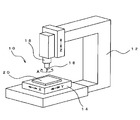
- This cutting machine 10 When performing by the milling method, for example, the cutting machine 10 shown in FIG. 1 is used.
- This cutting machine 10 has a U-shaped frame portion 12 having a side shape, and a lower portion 14 is provided with a table 14 movable in the X direction (left-right direction) and Y direction (front-rear direction).
- a resin substrate (resin substrate) 20 that is a base of the resin stamper of the present invention is fixed to 14.
- a main shaft portion 16 movable in the Z direction (vertical direction) is provided on the upper portion of the frame portion 12, and a cutting tool 18 is attached to the main shaft portion 16 so as to be rotatable in the arrow A direction.
- the movement operation in each direction is controlled by an NC control device (not shown) connected to the cutting machine.
- Data on the shape of the concavo-convex pattern is input to the NC control device in advance, and a relative positional relationship between the resin substrate 20 and the cutting tool 18 is created in accordance with the operation program.
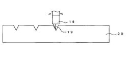
- the surface of the resin substrate 20 is cut into a desired concavo-convex pattern shape with the cutting edge 19 by rotating.
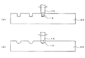
- the cross-sectional shape (V shape, square shape, U shape, etc.) of the concavo-convex pattern can be selected by changing the shape of the cutting edge 19 of the cutting tool 18 or the rotation axis as shown in FIGS. 3 (a) and 3 (b). It is.
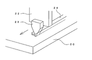
- the shaper method is a method of cutting the surface of the resin substrate 20 by controlling the relative position between the resin substrate 20 and the cutting tool 22 without rotating the cutting tool 22 as shown in FIG.
- This figure shows a state in which the groove 24 is formed by moving the cutting tool 22 in the direction of the arrow.
- the shaper method can be performed by a multi-axis control cutting machine having an NC controller.
- diamond cubic boron nitride, cermet, cemented carbide, ceramics, etc.
- cermet cubic boron nitride
- cemented carbide ceramics, etc.
- a fine uneven pattern is formed on the surface of the resin substrate.
- the size, such as the width and depth, of the fine concavo-convex pattern is appropriately selected according to the application. For example, cutting is possible within a range of several ⁇ m, and the size of the cutting tool is selected according to the size.
- the thickness of the resin substrate is appropriately set according to the depth of the uneven pattern.
- the film can be used from a thin film to a relatively thick plate, and specifically, for example, 1 ⁇ m to 10 mm.
- Cutting is not limited to the above-mentioned cutting machine, and can be performed using various conventionally known cutting machines.
- the material for the resin stamper for imprinting of the present invention is preferably a resin having a low surface energy from the viewpoint of releasability when used as a resin stamper.
- a resin having high ultraviolet transmittance is preferable in that it can be irradiated with ultraviolet rays from the stamper side to perform photoimprinting.
- a resin having a surface energy of 35 mN / m or less, preferably 20 to 30 mN / m is preferred, and a resin having an ultraviolet transmittance of 70% or more, preferably 80% or more at a wavelength of 365 nm is preferred.
- the preferable resin include hydrocarbon resins, fluorine resins, and silicone resins.
- the hydrocarbon-based resin refers to a resin composed of carbon and hydrogen, for example, an ⁇ -olefin homopolymer or copolymer, a cycloolefin homopolymer, or a mixture of different cycloolefins. Examples thereof include a copolymer or a copolymer of cycloolefin and ⁇ -olefin (cycloolefin resin).
- the ⁇ -olefin is preferably an ⁇ -olefin having 2 to 20 carbon atoms, and examples thereof include ethylene, propylene, 1-butene, 1-pentene, 4-methyl-1-pentene, 1-pentene and 1-hexene. It is done.
- Examples of the cycloolefin include norbornene, dicyclopentadiene, tetracyclododecene, ethyltetracyclododecene, and ethylidenetetracyclododecene.
- the fluorine-based resin refers to a resin containing a fluorine atom.
- examples include perfluoroalkyl vinyl ether copolymers, tetrafluoroethylene / ethylene copolymers, hexafluoropropylene / propylene copolymers, polyvinylidene fluoride, vinylidene fluoride / ethylene copolymers, and the like.
- silicone resin polydimethylsiloxane, diethylsiloxane, diphenylsiloxane, methylvinylsiloxane, ethylvinylsiloxane, phenylvinylsiloxane, ethylmethylsiloxane, methylphenylsiloxane, ethylphenylsiloxane, or the like can be applied.
- the 4-methyl-1-pentene resin includes 4-methyl-1-pentene homopolymer, 4-methyl-1-pentene and other monomers (such as the above-mentioned ⁇ -olefin).
- the proportion of 4-methyl-1-pentene is 60% by mass or more, preferably 80% by mass or more, particularly preferably 90% by mass, based on the mass of the copolymer. The above is preferable.
- a homopolymer of 4-methyl-1-pentene is preferable.
- 4-methyl-1-pentene resin is preferable is that it is not only excellent in releasability and ultraviolet transmittance but also has high durability as an imprint stamper. This is considered to be related to good mechanical properties such as tensile strength and elongation at break.
- the surface energy is calculated based on the contact angle obtained from a contact angle meter (Drop-master (manufactured by Kyowa Interface Co., Ltd.), standard solvent: water, 1-bromonaphthalene, diiodomethane). This is the value obtained by analysis by the geometric mean method based on the equation (Nasaaki Kitasaki, Toshio Hata et al., Journal of Japan Adhesion Association, Vol. 8 (3) 131-141 (1972)).
- additives such as lubricants, antioxidants, light stabilizers, plasticizers and the like may be added to the resin.
- Lubricants include alkyl polyoxyalkylene phosphate compounds, trialkyl phosphate phosphate compounds, phosphorus atom-containing compounds such as phosphates and phosphate amides, silicone resins such as unmodified or modified polysiloxanes, and fluoro (meth) acrylates. Fluorine atom-containing ethylenic compounds such as The addition amount of the lubricant is usually 0.01 to 5 parts by mass with respect to 100 parts by mass of the resin. By adding a lubricant, the releasability can be further improved.
- the antioxidant a known one can be used, but it is preferable to use a phenolic antioxidant from the viewpoint of not reducing the ultraviolet transmittance.
- phenolic antioxidants examples include pentaerythritol-tetrakis (3- (3,5-di-t-butyl-4-hydroxyphenyl) propionate), thiodiethylene-bis (3- (3,5-di-).
- pentaerythritol-tetrakis (3- (3,5-di-t-butyl-4-hydroxyphenyl) propionate), octadecyl-3- (3,5- Particularly preferred are di-t-butyl-4-hydroxyphenyl) propionate and ethylenebis (oxyethylene) bis (3- (5-t-butyl-4-hydroxy-m-tolyl) propionate).
- the resin stamper of the present invention preferably contains a light stabilizer in order to receive light, mainly ultraviolet rays, when used in the photoimprint method.
- a light stabilizer called a hindered amine type is preferably used.
- LA-52, LA-57, LA-62, LA-63LA-63p, LA-67, LA-68 (all of which are ADEKA)
- Tinuvin 744, Tinuvin 770, Tinuvin 765, Tinuvin 144, Tinuvin 622LD, CHIMASSORB 944LD (all manufactured by Ciba Specialty Chemicals), UV-3034 (manufactured by BF Goodrich), and the like.
- the light stabilizer may be used alone or in combination of two or more, and the blending amount is 0.01 to 5 parts by mass with respect to 100 parts by mass of the resin used. preferable.
- the above-mentioned additives may be used alone or in combination of two or more. Any method may be used for mixing these additives and the resin as long as the respective components can be mixed uniformly.
- a method of kneading these components in a molten state is a preferable method.
- the kneading apparatus can be performed using a closed kneading apparatus such as a Banbury mixer, a kneader, or an intermix, or an open kneading apparatus such as a mixing roll. After kneading, it is pelletized and film-formed by a known method such as a calendering method, an extrusion molding method, an inflation method, or a press molding method.
- the resin stamper of the present invention is suitable for optical imprinting. Optical imprinting can be performed by a normal method.
- the surface having the concavo-convex pattern of the resin stamper of the present invention is pressed against a photocurable resin composition layer formed on a product substrate, and the surface of the photocurable resin composition layer is the concavo-convex pattern.
- a laminate that adheres along the surface is formed.
- the resin stamper is removed to form an uneven pattern in which the uneven pattern of the resin stamper is reversed on the product substrate. . Thereby, an uneven
- any photocurable resin composition for forming a concavo-convex pattern using the resin stamper of the present invention may be used.
- a liquid composition that can be used in the nanoimprint process method is preferred.
- the viscosity is preferably 0.1 Pa ⁇ s to 100 Pa ⁇ s.
- the photocurable resin composition is preferably a composition containing a photocurable resin and a photoinitiator.
- photocurable resin examples include urethane acrylate, polyester acrylate, epoxy acrylate, epoxy resin, imide-based oligomer, and polyene / thiol-based oligomer.
- Urethane acrylates include, for example, diisocyanates such as hexamethylene diisocyanate, isophorone diisocyanate, methylene bis (4-cyclohexyl isocyanate), trimethylhexamethylene diisocyanate, tolylene diisocyanate, 4,4-diphenylmethane diisocyanate, xylylene diisocyanate, and poly (propylene oxide).
- diisocyanates such as hexamethylene diisocyanate, isophorone diisocyanate, methylene bis (4-cyclohexyl isocyanate), trimethylhexamethylene diisocyanate, tolylene diisocyanate, 4,4-diphenylmethane diisocyanate, xylylene diisocyanate, and poly (propylene oxide).
- Polyols such as diol, poly (propylene oxide) triol, poly (tetramethylene oxide) diol, ethoxylated bisphenol A and 2-hydroxyethyl acrylate 2-hydroxyethyl methacrylate, 2-hydroxypropyl acrylate, glycidol dimethacrylate, pentaerythritol tri Hydroxy acrylates such as acrylate Obtained by reacting, those having an acryloyl group and a urethane bond as a functional group in the molecule.
- polyester acrylate examples include polyester acrylate composed of phthalic anhydride, propylene oxide and acrylic acid, polyester acrylate composed of adipic acid, 1,6-hexanediol and acrylic acid, trimellitic acid, diethylene glycol and acrylic acid. And polyester acrylate.
- the epoxy acrylate is synthesized by reaction of an epoxy compound such as epichlorohydrin with acrylic acid or methacrylic acid.
- an epoxy compound such as epichlorohydrin with acrylic acid or methacrylic acid.
- bisphenol A type epoxy acrylate and bisphenol S synthesized by reaction of bisphenol A, epichlorohydrin and acrylic acid.
- Bisphenol S-type epoxy acrylate synthesized by reaction of chlorophenol, epichlorohydrin and acrylic acid bisphenol F-type epoxy acrylate synthesized by reaction of bisphenol F, epichlorohydrin and acrylic acid, synthesis by reaction of phenol novolac, epichlorohydrin and acrylic acid And phenol novolac type epoxy acrylate.
- epoxy resin examples include bisphenol type epoxy resins such as bisphenol A type epoxy resin, bisphenol F type epoxy resin, bisphenol AD type epoxy resin, and bisphenol S type epoxy resin; phenol novolac type epoxy resin, cresol novolak type epoxy resin and the like.
- examples include novolak-type epoxy resins; aromatic epoxy resins such as trisphenolmethane triglycidyl ether, and hydrogenated products and brominated products thereof.
- photopolymerization initiator a photoradical polymerization initiator and a photocationic polymerization initiator are preferable.
- the photoradical polymerization initiator include 4- (2-hydroxyethoxy) phenyl (2-hydroxy-2-propyl) ketone.
- Acetophenone derivatives such as ⁇ -hydroxy- ⁇ - ⁇ '-dimethylacetophenone, methoxyacetophenone and 2,2-dimethoxy-2-phenylacetophenone; benzoin ether compounds such as benzoin ethyl ether and benzoin propyl ether; benzyldimethyl ketal and the like Ketal derivatives; halogenated ketones, acyl phosphine oxides, acyl phosphonates, 2-methyl-1- [4- (methylthio) phenyl] -2-morpholinopropan-1-one, 2-benzyl-2-N, N-dimethylamino-1- ( 4-morpholinophenyl) -1-butane, bis (2,4,6-trimethylbenzoyl) -phenylphosphine oxide bis- (2,6-dimethoxybenzoyl) 2,4,4-trimethylpentylphosphine oxide, etc.
- Examples of the photocationic polymerization initiator include iron-allene complex compounds, aromatic diazonium salts, aromatic iodonium salts, aromatic sulfonium salts, onium salts, pyridinium salts, aluminum complexes / silanol salts, trichloromethyltriazine derivatives, and the like. It is done.
- Examples of the counter anion of the onium salt or pyridinium salt include SbF 6 ⁇ , PF 6 ⁇ , AsF 6 ⁇ , BF 4 ⁇ , tetrakis (pentafluoro) borate, trifluoromethane sulfonate, methane sulfonate, and trifluoro. Examples include acetate, acetate, sulfonate, tosylate, and nitrate.
- the addition amount of the photopolymerization initiator is generally 0.1 to 15 parts by weight, preferably 0.5 to 10 parts by weight with respect to 100 parts by weight of the photocurable resin.
- a reactive diluent may be added to the photocurable resin composition.
- the reactive diluent include 1,4-butanediol diacrylate, 1,6-hexanediol diacrylate, neopentyl, and the like.
- Glycol diacrylate 2- (2-ethoxyethoxy) ethyl acrylate, tetrahydrofurfuryl acrylate, 2-phenoxyethyl acrylate, diethylene glycol diacrylate, tetraethylene glycol diacrylate, 1,3-butylene glycol diacrylate, tripropylene glycol diacrylate , Trimethylolpropane triacrylate, pentaerythritol tetraacrylate, and hydroxypivalic acid neopentyl glycol diacrylate.
- the photo-curable resin composition further includes photopolymerization initiation assistants, thermal polymerization inhibitors, fillers, adhesion-imparting agents, thixotropic agents, plasticizers, colorants, etc. that are generally added as necessary. May be added.
- light sources that emit in the ultraviolet to visible range can be used as light sources, such as ultra-high pressure, high pressure, low pressure mercury, chemical lamps, xenon lamps, halogen lamps, Mercury halogen lamps, A carbon arc lamp, an incandescent lamp, a laser beam, etc. are mentioned.
- the irradiation time is not generally determined depending on the type of the lamp and the intensity of the light source, but is about 0.1 to several tens of seconds, preferably 0.5 to several seconds.
- the ultraviolet irradiation amount is preferably 300 mJ / cm 2 or more.
- the temperature during imprinting is determined in consideration of the dimensional change due to the heat of the stamper. For example, the ambient environment is maintained at 23 ° C., and the stamper / substrate temperature during imprinting is also maintained at 23 ° C. In this case, it is desirable that the intermediate mold is always produced at 23 ° C.
- the resin stamper of the present invention since the resin stamper of the present invention has high dimensional accuracy, the product substrate and the resin stamper can be precisely aligned, and a highly accurate uneven pattern can be formed on the product substrate. .
- partition walls, electronic devices (lithography, transistors), optical components (microlens arrays, waveguides, optical filters, photonic crystals) for information display panels such as high-quality electronic displays and electronic papers ), Bio-related materials (DNA chips, microreactors), recording media (patterned media, DVD) and the like can be advantageously obtained.
Landscapes
- Engineering & Computer Science (AREA)
- Chemical & Material Sciences (AREA)
- Nanotechnology (AREA)
- Physics & Mathematics (AREA)
- Crystallography & Structural Chemistry (AREA)
- Manufacturing & Machinery (AREA)
- General Physics & Mathematics (AREA)
- Condensed Matter Physics & Semiconductors (AREA)
- Mathematical Physics (AREA)
- Theoretical Computer Science (AREA)
- Shaping Of Tube Ends By Bending Or Straightening (AREA)
- Moulds For Moulding Plastics Or The Like (AREA)
- Manufacturing Optical Record Carriers (AREA)
- Exposure Of Semiconductors, Excluding Electron Or Ion Beam Exposure (AREA)
Abstract
微細な凹凸パターンが高い寸法精度で形成された樹脂製のインプリント用スタンパ及びその製造方法を提供することにある。 一方の表面に微細な凹凸パターンを有するインプリント用樹脂製スタンパであって、前記凹凸パターンが切削加工により形成されていることを特徴とするインプリント用樹脂スタンパ。
Description
本発明は、アライメント精度に優れたインプリント用樹脂スタンパ及びその製造方法並びにこの樹脂スタンパを用いた凹凸パターンの形成方法に関する。
近年、半導体デバイス、ディスプレイ、電子ペーパー、記録メディア、バイオチップ、光デバイスなどの製造工程における微細パターンの形成するための技術として、ナノインプリント技術が知られている。ナノインプリント技術は、従来のプレス技術と比較して、より微小な構造を実現するための微細加工の技術である。この技術自体には解像度に限界がなく、解像度はスタンパ(即ち金型)の作製精度によって決定される。したがって、高い精度のスタンパさえ作製できれば、従来のフォトリソグラフィーより容易に且つはるかに安価な装置を用いて、極微細構造を形成することが可能である。
インプリント技術には転写される材料により2種類に大別される。一方は、転写される材料を加熱し、スタンパ(金型)により塑性変形させた後、冷却してパターンを形成する熱インプリント技術である。もう一方は、基板上に室温で液状の光硬化性樹脂を塗布した後、光透過性のスタンパを樹脂に押し当て、光を照射させることで基板上の樹脂を硬化させパターンを形成する光インプリント技術である。特に光インプリント技術は室温にてパターン形成できるため熱による基板、スタンパ間の線膨張係数差による歪が発生しにくく、高精度のパターン形成が可能であり、半導体等のリソグラフィ技術の代替技術として注目を集めている。
インプリント技術では、パターン成形を安価に行うことができるが、マザースタンパである金型に樹脂が付着し易く、樹脂が付着した場合、そのスタンパを補修することは極めて困難である。金型が非常に高価なため、製造全体として安価とは言えない場合が多い。
その理由から、2工程によるインプリント法が用いられている。このインプリント法は、図5(a)に示すように、第1工程でマザースタンパ(金型)30の凹凸パターンが形成された表面を、加熱した熱可塑性樹脂フィルム32の表面に押圧した後、冷却して硬化させ、マザースタンパの凹凸パターンが反転された凹凸パターンを形成した中間スタンパ32aを得、次に、図5(b)に示すように、第二工程でこの中間スタンパ32aを、製品基板34上に塗布された光硬化性樹脂36に押圧して紫外線等により硬化させ、製品基板34上にマザースタンパと同一の凹凸パターン36aを得るというものである(特許文献1)。
この方法では、製品が樹脂製の中間スタンパを用いて成形されるため、マザースタンパ(テンプレート)には深刻な損傷が発生することはない。しかしながら、熱インプリント法で中間スタンパの作製する場合、硬化段階でマザースタンパと熱可塑性樹脂フィルム間の線膨張係数差に起因して、マザースタンパの寸法通りの中間スタンパを得られない場合がある。また、熱インプリント工程において、フィルムおよびスタンパを加熱・押圧・冷却する過程で面内に大きな温度バラツキが生じた場合、中間スタンパの面内全域にて良好な寸法精度の中間スタンパを得ることが困難になる。そして、中間スタンパの寸法精度が良好でない場合、特に高い寸法精度が要求される製品の製造時に、中間スタンパと製品基板とのアライメント工程に影響が出る。
即ち、製品基板と中間スタンパとのアライメント(位置合わせ)を行う場合、一般に、中間スタンパと製品基板に2個以上の位置合わせ用パターン(アライメントマークともいう)が形成されており、これらのマークを2点以上の位置合わせ用のカメラ(アライメントカメラともいう)で観察し、マークを合わせることで位置合わせを行う。しかしながら、上述したようにマザースタンパから中間スタンパへの転写工程において中間スタンパが収縮した場合、パターンの寸法に変化が生じ、2点以上のアライメントマークが合わなくなり、精確な位置合わせができなくなるという問題が生じる。また、あらかじめ収縮量を見込み、マザースタンパの寸法を補正する方法にてアライメントマークを合わせる方法もあるが、面内全域にて良好なアライメントを得ることは困難である。
従って、本発明の目的は、微細な凹凸パターンが高い寸法精度で形成された樹脂製のインプリント用スタンパ及びその製造方法を提供することにある。また、微細な凹凸パターンを製品の基板上の精確な位置に形成することが可能な凹凸パターン形成方法を提供することにある。
上記目的は、一方の表面に微細な凹凸パターンを有するインプリント用樹脂製スタンパであって、前記凹凸パターンが切削加工により形成されていることを特徴とするインプリント用樹脂スタンパにより達成される。
本発明の樹脂スタンパは、切削加工により凹凸パターンを形成しており、従来の中間スタンパのようにその作製過程において熱インプリント工程を必要としないため、硬化収縮による寸法変化が生じない。本発明の樹脂スタンパを使用してインプリントを行う場合、アライメントマーク及び面内全域の凹凸パターンを目的の位置に精確に形成できるため、そのアライメントを精確に行うことができ、製品基板上に凹凸パターンを精確な位置に形成することが可能となる。さらに、従来のようにマザースタンパを用いる必要がないため、製造コストの削減が図られる。
本発明の好ましい態様は以下の通りである。
(1)前記樹脂が、炭化水素系樹脂、フッ素系樹脂又はシリコーン系樹脂である。
樹脂基板の表面を精密に切削し、精確なパターンを形成することができる。また、これら樹脂は、表面エネルギーが低く、スタンパとして用いた場合の離型性に優れるので好ましい。
(2)前記樹脂が4-メチル-1-ペンテン系樹脂である。
上記樹脂の中でも特にポリメチルペンテンは、離型性及び紫外線透過性に優れているだけでなく、インプリント用スタンパとしての耐久性にも優れている。
(3)切削加工がミーリング方式又はシェーパー方式で行われる。
これらの方式を用いれば精密に切削を行うことができる。
(4)光インプリント用樹脂スタンパである。
インプリント時において樹脂スタンパ側から紫外線を照射可能であるため、光インプリント用の樹脂スタンパとして好適である。
また、本目的は、一方の表面に微細な凹凸パターンを有するインプリント用樹脂製スタンパの製造方法であって、前記凹凸パターンの形状に関するデータが入力されたNC制御装置を有する切削加工機の加工処理部に樹脂製の基板を載置する工程、及び次いで前記切削加工機を用いて、前記樹脂製の基板の表面を前記入力された凹凸パターンの形状に関するデータに従う切削処理に付す工程、を含むインプリント用樹脂スタンパの製造方法により達成される。
更に、本目的は、上記樹脂スタンパの前記凹凸パターンを有する表面を、製品用の基板の上に形成した光硬化性樹脂組成物層に押圧して、該光硬化性樹脂組成物層の表面が前記凹凸パターン表面に沿って密着した積層体を形成する工程、前記樹脂スタンパを有する積層体の前記光硬化性樹脂組成物層を光によって硬化させる工程、及び前記樹脂スタンパを除去することにより、製品用の基板の上に前記凹凸パターンの反転凹凸パターンを形成する工程、を含む凹凸パターン形成方法により達成される。
本発明の樹脂スタンパは微細凹凸パターンの寸法精度が良好であり、インプリントにおいて製品用の基板とのアライメントを精確に行うことが可能である。従って、本発明の樹脂スタンパを用いれば、微細凹凸パターンが精確に形成された、電子ディスプレイリブ、電子デバイス(リソグラフィ、トランジスタ)、光学部品(マイクロレンズアレイ、導波路、光学フィルタ、フォトニックス結晶)、バイオ関連材料(DNAチップ、マイクロリアクタ)、記録媒体(パターンドメディア、DVD)を有利に得ることができる。
以下、本発明について詳細に説明する。
[切削加工]
上述したように、本発明のインプリント用樹脂スタンパは、その表面に凹凸パターンを切削加工によって形成することにより作製される。切削加工はミーリング方式やシェーパー方式等で行うことができる。
上述したように、本発明のインプリント用樹脂スタンパは、その表面に凹凸パターンを切削加工によって形成することにより作製される。切削加工はミーリング方式やシェーパー方式等で行うことができる。
ミーリング方式で行う場合、例えば図1に示す切削加工機10を使用する。この切削加工機10は、側面形状コの字型のフレーム部12を有し、下部にはX方向(左右方向)及びY方向(前後方向)に移動可能なテーブル14が設けられており、テーブル14には本発明の樹脂スタンパの元となる樹脂製の基板(樹脂基板)20が固定されている。また、フレーム部12の上部にはZ方向(上下方向)に移動可能な主軸部16を備えており、その主軸部16には切削工具18が矢印A方向に回転可能に取り付けられている。それぞれの方向への移動動作は、切削加工機に接続されているNC制御装置(図示せず)により制御される。予め凹凸パターンの形状のデータをNC制御装置に入力し、その動作プログラムに沿って、樹脂基板20と切削工具18との相対的な位置関係を作り、図2に示すように、切削工具18を回転させて切れ刃19で樹脂基板20の表面を所望の凹凸パターン形状に切削する。凹凸パターンの断面形状(V状、角状、U状等)は、図3(a)及び(b)に示すように切削工具18の切れ刃19の形状、あるいは回転軸の変更等により選択可能である。
一方、シェーパー方式は、図4に示すように、切削工具22は回転せず、樹脂基板20と切削工具22との相対位置を制御することにより樹脂基板20の表面を切削する方法である。本図では矢印方向に切削工具22を移動させて溝部24を形成する様子を示している。シェーパー方式はNC制御装置を有する多軸制御可能な切削加工機で行うことができる。
切削工具の切れ刃の材質としては、ダイヤモンド、立方晶窒化ホウ素、サーメット、超硬合金、セラミックス等を用いることができるが、精密に切削を行うことができる点でダイヤモンド工具を用いることが好ましい。
以上のようにして樹脂基板の表面に微細な凹凸パターンを形成する。微細な凹凸パターンの幅及び深さ等のサイズは用途に応じて適宜選択する。例えば、数μmの範囲で切削可能であり、そのサイズに応じて切削工具のサイズを選択する。
なお、樹脂の基板の厚さは、凹凸パターンの深さに応じて適宜設定する。例えば、フィルム状の薄い厚さのものから比較的厚みのある板状のものまで使用可能であり、具体的には例えば1μm~10mmである。切削加工は上記切削加工機に限定されるものではなく、従来から公知の種々の切削加工機を用いて行うことが可能である。
また、切削加工時には、熱による樹脂基板の寸法変化を避けるため、樹脂基板の温度を、光インプリント成形時の温度と同一にしたほうがよく、切削加工機の設置環境・加工機温度・切削オイル等の温度も考慮する必要がある。
[樹脂スタンパ用材料]
本発明のインプリント用樹脂スタンパの材料としては、樹脂スタンパとして使用した場合の離型性の点から表面エネルギーが低い樹脂が好ましい。また、紫外線をスタンパ側から照射して光インプリントを行うことができる点で紫外線透過性が高い樹脂が好ましい。
本発明のインプリント用樹脂スタンパの材料としては、樹脂スタンパとして使用した場合の離型性の点から表面エネルギーが低い樹脂が好ましい。また、紫外線をスタンパ側から照射して光インプリントを行うことができる点で紫外線透過性が高い樹脂が好ましい。
例えば、表面エネルギーが35mN/m以下、好ましくは20~30mN/mである樹脂が好ましく、また、紫外線透過率が、波長365nmで70%以上、好ましくは80%以上である樹脂が好ましい。
上記好ましい樹脂の具体例として、炭化水素系樹脂、フッ素系樹脂及びシリコーン系樹脂が挙げられる。本発明において、炭化水素系樹脂とは、炭素と水素から構成される樹脂のことをいい、例えば、α-オレフィンの単独重合体又は共重合体、シクロオレフィンの単独重合体又は異なるシクロオレフィン同士の共重合体若しくはシクロオレフィンとα-オレフィンとの共重合体(シクロオレフィン系樹脂)が挙げられる。α-オレフィンとしては、炭素原子数2~20のα-オレフィンが好ましく、例えばエチレン、プロピレン、1-ブテン、1-ペンテン、4-メチル-1-ペンテン、1-ペンテン、1-ヘキセン等が挙げられる。シクロオレフィンとしては、ノルボルネン、ジシクロペンタジエン、テトラシクロドデセン、エチルテトラシクロドデセン、エチリデンテトラシクロドデセン等が挙げられる。
また、フッ素系樹脂とは、フッ素原子を含有する樹脂のことをいい、例えば、ポリテトラフルオロエチレン、ポリフッ化ビニリデン、ポリヘキサフルオロプロピレン、テトラフルオロエチレン/ヘキサフルオロプロピレン共重合体、テトラフルオロエチレン/パーフルオロアルキルビニルエーテル共重合体、テトラフルオロエチレン/エチレン共重合体、ヘキサフルオロプロピレン/プロピレン共重合体、ポリビニリデンフルオライド、ビニリデンフルオライド/エチレン共重合体などが挙げられる。
また、シリコーン系樹脂としては、ポリジメチルシロキサン、ジエチルシロキサン、ジフェニルシロキサン、メチルビニルシロキサン、エチルビニルシロキサン、フェニルビニルシロキサン、エチルメチルシロキサン、メチルフェニルシロキサン、エチルフェニルシロキサン等を適用することができる。
これら離型性に優れる樹脂を用いれば、離型性を向上させるために表面処理を行う必要はないため、樹脂スタンパの作製工程の増加減少や費用削減効果が図られる。
上記列挙した樹脂のうち、ポリプロピレン、ポリエチレン、4-メチル-1-ペンテン系樹脂、シクロオレフィン系樹脂及びフッ素系樹脂が好ましく、中でも4-メチル-1-ペンテン系樹脂が特に好ましい。ここで、4-メチル-1-ペンテン系樹脂には、4-メチル-1-ペンテンの単独重合体の他、4-メチル-1-ペンテンと他のモノマー(上述のα-オレフィン等)との共重合体が含まれ、共重合体の場合、4-メチル-1-ペンテンの割合がその共重合体の質量に対して60質量%以上、好ましくは80質量%以上、特に好ましくは90%質量以上が好ましい。特に4-メチル-1-ペンテンの単独重合体が好ましい。4-メチル-1-ペンテン系樹脂が好ましい理由は、離型性及び紫外線透過性に優れるだけでなく、インプリント用スタンパとしての耐久性が高いことによる。これは、引張強度や破断伸び等の良好な機械的特性が関係しているものと考えられる。
ここで、上記表面エネルギーは、接触角計(Drop-master(協和界面社製)、標準溶媒:水、1-ブロモナフタレン、ジヨードメタン)により得られた接触角の数値から、北崎、畑の拡張Fowkes式に基づく幾何学平均法による解析(北崎寧昭、畑敏雄ら、日本接着協会誌、第8巻(3)131-141頁(1972年))で求めた値をいう。
上記樹脂には、種々の添加剤、例えば、滑剤、酸化防止剤、光安定剤、可塑剤等を添加してもよい。
滑剤としては、リン酸アルキルポリオキシアルキレン化合物、リン酸トリアルキルエステル化合物、リン酸塩及びリン酸アミド等のリン原子含有化合物、非変性又は変性ポリシロキサン等のシリコーン系樹脂、フルオロ(メタ)アクリレート類等のフッ素原子含有エチレン性化合物が挙げられる。滑剤の添加量は、樹脂100質量部に対し、通常0.01~5質量部である。滑剤を添加することで、更に離形性を向上させることができる。
酸化防止剤としては、公知のものを用いることができるが、紫外線透過性を低下させない点から、フェノール系酸化防止剤を用いるのが好ましい。
フェノール系酸化防止剤としては、例えば、ペンタエリスリトール-テトラキス(3-(3,5-ジ-t-ブチル-4-ヒドロキシフェニル)プロピオネート)、チオジエチレン-ビス(3-(3,5-ジ-t-ブチル-4-ヒドロキシフェニル)プロピオネート)、オクタデシル-3-(3,5-ジ-t-ブチル-4-ヒドロキシフェニル)プロピオネート、N,N’-ヘキサン-1,6-ジイルビス(3-(3,5-ジ-t-ブチル-4-ヒドロキシフェニル)プロピオナミド)、ジエチル((3,5-ビス(1,1-ジメチルエチル)-4-ヒドロキシフェニル)メチル)ホスフェート、3,3’,3'',5,5’,5''-ヘキサ-t-ブチル-a,a’,a''-(メシチレン-2,4,6-トリイル)トリ-p-クレゾール、エチレンビス(オキシエチレン)ビス(3-(5-t-ブチル-4-ヒドロキシ-m-トリル)プロピオネート)、ヘキサメチレン-ビス(3-(3,5-ジ-t-ブチル-4-ヒドロキシフェニル)プロピオネート)、1,3,5-トリス(3,5-ジ-t-ブチル-4-ヒドロキシベンジル)-1,3,5-トリアジン-2,4,6(1H,3H,5H)-トリオン、1,3,5-トリス((4-t-ブチル-3-ヒドロキシ-2,6-キシリル)メチル)-1,3,5-トリアジン-2,4,6(1H,3H,5H)-トリオン、2,6-ジ-t-ブチル-4-(4,6-ビス(オクチルチオ)-1,3,5-トリアジン-2-イルアミノ)フェノール、3,9-ビス(2-(3-(3-t-ブチル-4-ヒドロキシ-5-メチルフェニル)プロピオニルオキシ)-1,1-ジメチルエチル)-2,4,8,10-テトラオキサスピロ(5,5)ウンデカンなどが挙げられる。その中でも、極めて透明性に優れたものとなることから、ペンタエリスリトール-テトラキス(3-(3,5-ジ-t-ブチル-4-ヒドロキシフェニル)プロピオネート)、オクタデシル-3-(3,5-ジ-t-ブチル-4-ヒドロキシフェニル)プロピオネート、エチレンビス(オキシエチレン)ビス(3-(5-t-ブチル-4-ヒドロキシ-m-トリル)プロピオネート)であることが特に好ましい。
また、本発明の樹脂スタンパは、光インプリント法に使用するに際し、光、主に紫外線の照射を受けるために光安定剤を含むことが好ましい。
光安定剤としては、ヒンダードアミン系と呼ばれる光安定剤を用いることが好ましく、例えば、LA-52、LA-57、LA-62、LA-63LA-63p、LA-67、LA-68(いずれもADEKA社製)、Tinuvin744、Tinuvin 770、Tinuvin 765、Tinuvin144、Tinuvin 622LD、CHIMASSORB 944LD(いずれもチバ・スペシャリティ・ケミカルズ社製)、UV-3034(B.F.グッドリッチ社製)等を挙げることができる。なお、上記光安定剤は、単独で使用しても、2種以上組み合わせて用いてもよく、その配合量は、使用する樹脂100質量部に対して0.01~5質量部であることが好ましい。
上述した添加剤は1種単独で使用してもよく、2種以上を混合して使用してもよい。これら添加剤と樹脂との混合は、各成分が均一に混合できればどのような方法を用いてもよく、例えば、これら成分を溶融状態で混練する方法が好適な方法として挙げられる。混練装置は、バンバリーミキサー、ニーダー、インターミックスなどの密閉式混練装置、ミキシングロールなどの開放式混練装置を用いて行うことができる。混練後、ペレット化して、カレンダー法、押出成形法、インフレーション法、プレス成形法等の公知の方法でフィルム成形する。
[本発明の樹脂スタンパを用いたインプリント]
以下、上記作製した本発明の樹脂スタンパを用いて製品基板上に凹凸パターンを形成する手順について説明する。本発明の樹脂スタンパは光インプリントに好適である。光インプリントは通常の方法で行うことが可能である。
以下、上記作製した本発明の樹脂スタンパを用いて製品基板上に凹凸パターンを形成する手順について説明する。本発明の樹脂スタンパは光インプリントに好適である。光インプリントは通常の方法で行うことが可能である。
まず、本発明の樹脂スタンパの凹凸パターンを有する表面を、製品用の基板の上に形成した光硬化性樹脂組成物層に押圧して、該光硬化性樹脂組成物層の表面が前記凹凸パターン表面に沿って密着した積層体を形成する。次に、その積層体の光硬化性樹脂組成物層を光によって硬化させた後、樹脂スタンパを除去することにより、製品用の基板の上に樹脂スタンパの凹凸パターンが反転した凹凸パターンを形成する。これにより、製品基板上に凹凸パターンを形成することができる。
本発明の方法において、本発明の樹脂スタンパを用いて凹凸パターンを形成するための光硬化性樹脂組成物はどのようなものでも良い。特にナノインプリントプロセス法に使用できる液状組成物が好ましい。液状組成物の場合、粘度は0.1Pa・s~100Pa・sが好ましい。光硬化性樹脂組成物は光硬化性樹脂と光開始剤を含む組成物が好ましい。
光硬化性樹脂としては、例えば、ウレタンアクリレート、ポリエステルアクリレート、エポキシアクリレート、エポキシ樹脂、イミド系オリゴマー、ポリエン・チオール系オリゴマー等が挙げられる。
ウレタンアクリレートは、例えば、ヘキサメチレンジイソシアネート、イソホロンジイソシアネート、メチレンビス(4-シクロヘキシルイソシアネート)、トリメチルヘキサメチレンジイソシアネート、トリレンジイソシアネート、4,4-ジフェニルメタンジイソシアネート、キシリレンジイソシアネート等のジイソシアネート類とポリ(プロピレンオキサイド)ジオール、ポリ(プロピレンオキサイド)トリオール、ポリ(テトラメチレンオキサイド)ジオール、エトキシ化ビスフェノールA等のポリオール類と2-ヒドロキシエチルアクリレート2-ヒドロキシエチルメタクリレート、2-ヒドロキシプロピルアクリレート、グリシドールジメタクリレート、ペンタエリスリトールトリアクリレート等のヒドロキシアクリレート類とを反応させることによって得られ、分子中に官能基としてアクリロイル基とウレタン結合を有するものである。
ポリエステルアクリレートとしては、例えば、無水フタル酸とプロピレンオキサイドとアクリル酸とからなるポリエステルアクリレート、アジピン酸と1,6-ヘキサンジオールとアクリル酸とからなるポリエステルアクリレート、トリメリット酸とジエチレングリコールとアクリル酸とからなるポリエステルアクリレート等が挙げられる。
エポキシアクリレートは、エピクロルヒドリン等のエポキシ化合物とアクリル酸又はメタクリル酸との反応により合成されたものであり、例えば、ビスフェノールAとエピクロルヒドリンとアクリル酸との反応により合成されるビスフェノールA型エポキシアクリレート、ビスフェノールSとエピクロルヒドリンとアクリル酸との反応により合成されるビスフェノールS型エポキシアクリレート、ビスフェノールFとエピクロルヒドリンとアクリル酸との反応により合成されるビスフェノールF型エポキシアクリレート、フェノールノボラックとエピクロルヒドリンとアクリル酸との反応により合成されるフェノールノボラック型エポキシアクリレート等が挙げられる。
エポキシ樹脂としては、例えば、ビスフェノールA型エポキシ樹脂、ビスフェノールF型エポキシ樹脂、ビスフェノールAD型エポキシ樹脂、ビスフェノールS型エポキシ樹脂等のビスフェノール型エポキシ樹脂;フェノールノボラック型エポキシ樹脂、クレゾールノボラック型エポキシ樹脂等のノボラック型エポキシ樹脂;トリスフェノールメタントリグリシジルエーテル等の芳香族エポキシ樹脂、及び、これらの水添化物や臭素化物等が挙げられる。
光重合開始剤としては、光ラジカル重合開始剤及び光カチオン重合開始剤が好ましく、光ラジカル重合開始剤としては、例えば、4-(2-ヒドロキシエトキシ)フェニル(2-ヒドロキシ-2-プロピル)ケトン、α-ヒドロキシ-α-α’-ジメチルアセトフェノン、メトキシアセトフェノン、2,2-ジメトキシ-2-フェニルアセトフェノン等のアセトフェノン誘導体;ベンゾインエチルエーテル、ベンゾインプロピルエーテル等のベンゾインエーテル系化合物;ベンジルジメチルケタール等のケタール誘導体;ハロゲン化ケトン、アシルフォスフィンオキシド、アシルフォスフォナート、2-メチル-1-[4-(メチルチオ)フェニル]-2-モルフォリノプロパン-1-オン、2-ベンジル-2-N,N-ジメチルアミノ-1-(4-モルフォリノフェニル)-1-ブタン、ビス(2,4,6-トリメチルベンゾイル)-フェニルフォスフィンオキシドビス-(2,6-ジメトキシベンゾイル)2,4,4-トリメチルペンチルフォスフィンオキシド、等が挙げられる。光カチオン重合開始剤としては、例えば、鉄-アレン錯体化合物、芳香族ジアゾニウム塩、芳香族ヨードニウム塩、芳香族スルホニウム塩、オニウム塩、ピリジニウム塩、アルミニウム錯体/シラノール塩、トリクロロメチルトリアジン誘導体等が挙げられる。上記オニウム塩やピリジニウム塩の対アニオンとしては、例えば、SbF6-、PF6-、AsF6-、BF4-、テトラキス(ペンタフルオロ)ボレート、トリフルオロメタンスルフォネート、メタンスルフォネート、トリフルオロアセテート、アセテート、スルフォネート、トシレート、ナイトレート等が挙げられる。
光重合開始剤の添加量は、一般に光硬化性樹脂100重量部に対して、0.1~15重量部であり、好ましくは、0.5~10重量部である。
上記光硬化性樹脂組成物には、反応性希釈剤が添加されてもよく、反応性希釈剤としては、例えば、1,4-ブタンジオールジアクリレート、1,6-ヘキサンジオールジアクリレート、ネオペンチルグリコールジアクリレート、2-(2-エトキシエトキシ)エチルアクリレート、テトラヒドロフルフリルアクリレート、2-フェノキシエチルアクリレート、ジエチレングリコールジアクリレート、テトラエチレングリコールジアクリレート、1,3-ブチレングリコールジアクリレート、トリプロピレングリコールジアクリレート、トリメチロールプロパントリアクリレート、ペンタエリスリトールテトラアクリレート、ヒドロキシピバリン酸ネオペンチルグリコールジアクリレート等が挙げられる。
上記光硬化性樹脂組成物には、更に、必要に応じて、一般に添加されている光重合開始助剤、熱重合禁止剤、充填剤、接着付与剤、チクソ付与剤、可塑剤、着色剤等が添加されてもよい。
光硬化性樹脂を硬化する場合は、光源として紫外~可視領域に発行する多くのものが採用でき、例えば、超高圧、高圧、低圧水銀当、ケミカルランプ、キセノンランプ、ハロゲンランプ、マーキュリーハロゲンランプ、カーボンアーク灯、白熱灯、レーザ光等が挙げられる。照射時間は、ランプの種類、光源の強さによって一概には決められないが、0.1秒~数十秒程度、好ましくは0.5~数秒である。紫外線照射量は300mJ/cm2以上が好ましい。インプリント時の温度はスタンパの熱による寸法変化を考慮して決める。例えば周囲の環境を23℃に保ち、インプリント時のスタンパ・基板温度も23℃に保つようにする。この場合は中間型作製も常に23℃にて行うのが望ましい。
なお、上記インプリントにおいて、本発明の樹脂スタンパは寸法精度が高いため、製品基板と樹脂スタンパとのアライメントを精密に行うことができ、製品基板上に高精度な凹凸パターンを形成することができる。
本発明の樹脂スタンパを用いれば、高品質な電子ディスプレイ、電子ペーパー等の情報表示用パネルの隔壁や電子デバイス(リソグラフィ、トランジスタ)、光学部品(マイクロレンズアレイ、導波路、光学フィルタ、フォトニックス結晶)、バイオ関連材料(DNAチップ、マイクロリアクタ)、記録媒体(パターンドメディア、DVD)等を有利に得ることができる。
10 切削加工機
12 フレーム部
14 テーブル
16 主軸部
18 切削工具
19 切れ刃
20 樹脂基板
22 切削工具
23 切れ刃
24 溝部
12 フレーム部
14 テーブル
16 主軸部
18 切削工具
19 切れ刃
20 樹脂基板
22 切削工具
23 切れ刃
24 溝部
Claims (7)
- 一方の表面に微細な凹凸パターンを有するインプリント用樹脂製スタンパであって、
前記凹凸パターンが切削加工により形成されていることを特徴とするインプリント用樹脂スタンパ。 - 前記樹脂が、炭化水素系樹脂、フッ素系樹脂又はシリコーン系樹脂であることを特徴とする請求項1に記載のインプリント用樹脂スタンパ。
- 前記樹脂が4-メチル-1ペンテン系樹脂であることを特徴とする請求項1又は2に記載の樹脂スタンパ。
- 前記切削加工が、ミーリング方式又はシェーパー方式で行われることを特徴とする請求項1~3の何れか1項に記載の樹脂スタンパ。
- 光インプリント用樹脂スタンパである請求項1~4の何れか1項に記載の樹脂スタンパ。
- 一方の表面に微細な凹凸パターンを有するインプリント用樹脂製スタンパの製造方法であって、
前記凹凸パターンの形状に関するデータが入力されたNC制御装置を有する切削加工機の加工処理部に樹脂製の基板を載置する工程、及び
次いで前記切削加工機を用いて、前記樹脂製の基板の表面を前記凹凸パターンの形状に関するデータに従う切削処理に付す工程、
を含むインプリント用樹脂スタンパの製造方法。 - 請求項1~5の何れか1項に記載の樹脂スタンパの前記凹凸パターンを有する表面を、製品用の基板の上に形成した光硬化性樹脂組成物層に押圧して、該光硬化性樹脂組成物層の表面が前記凹凸パターン表面に沿って密着した積層体を形成する工程、
前記樹脂スタンパを有する積層体の前記光硬化性樹脂組成物層を光によって硬化させる工程、及び
前記樹脂スタンパを除去することにより、製品用の基板の上に前記凹凸パターンの反転凹凸パターンを形成する工程、
を含む凹凸パターン形成方法。
Applications Claiming Priority (2)
| Application Number | Priority Date | Filing Date | Title |
|---|---|---|---|
| JP2011-044652 | 2011-03-02 | ||
| JP2011044652A JP2012181895A (ja) | 2011-03-02 | 2011-03-02 | インプリント用樹脂スタンパ及びその製造方法 |
Publications (1)
| Publication Number | Publication Date |
|---|---|
| WO2012117892A1 true WO2012117892A1 (ja) | 2012-09-07 |
Family
ID=46757831
Family Applications (1)
| Application Number | Title | Priority Date | Filing Date |
|---|---|---|---|
| PCT/JP2012/054112 Ceased WO2012117892A1 (ja) | 2011-03-02 | 2012-02-21 | インプリント用樹脂スタンパ及びその製造方法 |
Country Status (3)
| Country | Link |
|---|---|
| JP (1) | JP2012181895A (ja) |
| TW (1) | TW201300226A (ja) |
| WO (1) | WO2012117892A1 (ja) |
Cited By (2)
| Publication number | Priority date | Publication date | Assignee | Title |
|---|---|---|---|---|
| JP2016051493A (ja) * | 2014-08-29 | 2016-04-11 | 富士フイルム株式会社 | 磁気記録媒体 |
| JP2017045501A (ja) * | 2016-12-07 | 2017-03-02 | 富士フイルム株式会社 | 磁気記録媒体 |
Families Citing this family (2)
| Publication number | Priority date | Publication date | Assignee | Title |
|---|---|---|---|---|
| JP6015559B2 (ja) * | 2013-05-27 | 2016-10-26 | 富士ゼロックス株式会社 | レンズアレイ製造装置及びレンズアレイ製造方法 |
| JP6317247B2 (ja) * | 2014-12-22 | 2018-04-25 | 富士フイルム株式会社 | インプリント用モールド |
Citations (5)
| Publication number | Priority date | Publication date | Assignee | Title |
|---|---|---|---|---|
| JPH02205975A (ja) * | 1989-02-03 | 1990-08-15 | Sony Corp | 型製造方法 |
| JP2003022586A (ja) * | 2001-05-01 | 2003-01-24 | Tdk Corp | 光情報媒体の製造方法 |
| JP2006198883A (ja) * | 2005-01-20 | 2006-08-03 | Asahi Glass Co Ltd | モールドおよび表面に微細パターンを有する物品 |
| WO2009139448A1 (ja) * | 2008-05-16 | 2009-11-19 | 昭和電工株式会社 | パターン形成方法 |
| JP2010082832A (ja) * | 2008-09-29 | 2010-04-15 | Nissha Printing Co Ltd | 切削加工によるナノインプリント用金型 |
-
2011
- 2011-03-02 JP JP2011044652A patent/JP2012181895A/ja not_active Withdrawn
-
2012
- 2012-02-21 WO PCT/JP2012/054112 patent/WO2012117892A1/ja not_active Ceased
- 2012-03-01 TW TW101106642A patent/TW201300226A/zh unknown
Patent Citations (5)
| Publication number | Priority date | Publication date | Assignee | Title |
|---|---|---|---|---|
| JPH02205975A (ja) * | 1989-02-03 | 1990-08-15 | Sony Corp | 型製造方法 |
| JP2003022586A (ja) * | 2001-05-01 | 2003-01-24 | Tdk Corp | 光情報媒体の製造方法 |
| JP2006198883A (ja) * | 2005-01-20 | 2006-08-03 | Asahi Glass Co Ltd | モールドおよび表面に微細パターンを有する物品 |
| WO2009139448A1 (ja) * | 2008-05-16 | 2009-11-19 | 昭和電工株式会社 | パターン形成方法 |
| JP2010082832A (ja) * | 2008-09-29 | 2010-04-15 | Nissha Printing Co Ltd | 切削加工によるナノインプリント用金型 |
Cited By (2)
| Publication number | Priority date | Publication date | Assignee | Title |
|---|---|---|---|---|
| JP2016051493A (ja) * | 2014-08-29 | 2016-04-11 | 富士フイルム株式会社 | 磁気記録媒体 |
| JP2017045501A (ja) * | 2016-12-07 | 2017-03-02 | 富士フイルム株式会社 | 磁気記録媒体 |
Also Published As
| Publication number | Publication date |
|---|---|
| TW201300226A (zh) | 2013-01-01 |
| JP2012181895A (ja) | 2012-09-20 |
Similar Documents
| Publication | Publication Date | Title |
|---|---|---|
| US6932934B2 (en) | Formation of discontinuous films during an imprint lithography process | |
| JP5215833B2 (ja) | 微細パターン転写用スタンパ及びその製造方法 | |
| US8132505B2 (en) | Imprint apparatus and imprint method | |
| US6900881B2 (en) | Step and repeat imprint lithography systems | |
| US8318066B2 (en) | Step and repeat imprint lithography process | |
| JP5555025B2 (ja) | 微細パターン転写用スタンパ及びその製造方法 | |
| US20040009673A1 (en) | Method and system for imprint lithography using an electric field | |
| JP2011240643A (ja) | 樹脂製フィルムを用いた凹凸パターンの形成方法、その方法に使用する装置 | |
| CN1668437A (zh) | 平板印刷术的工艺和系统 | |
| JP2011066100A (ja) | 光硬化性転写シート、及びこれを用いた凹凸パターンの形成方法 | |
| WO2010001538A1 (ja) | 微細構造体およびインプリント用スタンパ | |
| CN101051182A (zh) | 压印光刻的校准 | |
| Peng et al. | Continuous roller nanoimprinting: next generation lithography | |
| WO2014084030A1 (ja) | 微細構造体の製造方法及びナノインプリント用光硬化性組成物 | |
| JP2012181895A (ja) | インプリント用樹脂スタンパ及びその製造方法 | |
| JP6010481B2 (ja) | フィルム状モールドの製造方法 | |
| JP2013110196A (ja) | 樹脂フィルムと基板とのアライメント方法 | |
| Taniguchi et al. | Nanoimprint technology: nanotransfer for thermoplastic and photocurable polymers | |
| JP5687857B2 (ja) | ナノインプリント用樹脂スタンパ及びこれを使用したナノインプリント装置 | |
| KR100934239B1 (ko) | 임프린트용 대면적 스탬프 제작방법 | |
| JP2015050443A (ja) | 微細構造転写装置 | |
| JP2006023376A (ja) | 光デバイスの製造方法 | |
| JP2018029101A (ja) | インプリント装置、および物品製造方法 | |
| JP2006003622A (ja) | 光デバイスの製造方法 | |
| WO2012111590A1 (ja) | インプリント装置 |
Legal Events
| Date | Code | Title | Description |
|---|---|---|---|
| 121 | Ep: the epo has been informed by wipo that ep was designated in this application |
Ref document number: 12751840 Country of ref document: EP Kind code of ref document: A1 |
|
| NENP | Non-entry into the national phase |
Ref country code: DE |
|
| 122 | Ep: pct application non-entry in european phase |
Ref document number: 12751840 Country of ref document: EP Kind code of ref document: A1 |