WO2012117802A1 - 露光装置及びマイクロレンズアレイ構造体 - Google Patents
露光装置及びマイクロレンズアレイ構造体 Download PDFInfo
- Publication number
- WO2012117802A1 WO2012117802A1 PCT/JP2012/052379 JP2012052379W WO2012117802A1 WO 2012117802 A1 WO2012117802 A1 WO 2012117802A1 JP 2012052379 W JP2012052379 W JP 2012052379W WO 2012117802 A1 WO2012117802 A1 WO 2012117802A1
- Authority
- WO
- WIPO (PCT)
- Prior art keywords
- substrate
- exposure
- microlens array
- light
- exposure light
- Prior art date
- Legal status (The legal status is an assumption and is not a legal conclusion. Google has not performed a legal analysis and makes no representation as to the accuracy of the status listed.)
- Ceased
Links
Images



Classifications
-
- G—PHYSICS
- G03—PHOTOGRAPHY; CINEMATOGRAPHY; ANALOGOUS TECHNIQUES USING WAVES OTHER THAN OPTICAL WAVES; ELECTROGRAPHY; HOLOGRAPHY
- G03F—PHOTOMECHANICAL PRODUCTION OF TEXTURED OR PATTERNED SURFACES, e.g. FOR PRINTING, FOR PROCESSING OF SEMICONDUCTOR DEVICES; MATERIALS THEREFOR; ORIGINALS THEREFOR; APPARATUS SPECIALLY ADAPTED THEREFOR
- G03F7/00—Photomechanical, e.g. photolithographic, production of textured or patterned surfaces, e.g. printing surfaces; Materials therefor, e.g. comprising photoresists; Apparatus specially adapted therefor
- G03F7/70—Microphotolithographic exposure; Apparatus therefor
- G03F7/70216—Mask projection systems
-
- G—PHYSICS
- G02—OPTICS
- G02B—OPTICAL ELEMENTS, SYSTEMS OR APPARATUS
- G02B3/00—Simple or compound lenses
- G02B3/0006—Arrays
- G02B3/0037—Arrays characterized by the distribution or form of lenses
- G02B3/0056—Arrays characterized by the distribution or form of lenses arranged along two different directions in a plane, e.g. honeycomb arrangement of lenses
-
- G—PHYSICS
- G03—PHOTOGRAPHY; CINEMATOGRAPHY; ANALOGOUS TECHNIQUES USING WAVES OTHER THAN OPTICAL WAVES; ELECTROGRAPHY; HOLOGRAPHY
- G03F—PHOTOMECHANICAL PRODUCTION OF TEXTURED OR PATTERNED SURFACES, e.g. FOR PRINTING, FOR PROCESSING OF SEMICONDUCTOR DEVICES; MATERIALS THEREFOR; ORIGINALS THEREFOR; APPARATUS SPECIALLY ADAPTED THEREFOR
- G03F7/00—Photomechanical, e.g. photolithographic, production of textured or patterned surfaces, e.g. printing surfaces; Materials therefor, e.g. comprising photoresists; Apparatus specially adapted therefor
- G03F7/70—Microphotolithographic exposure; Apparatus therefor
- G03F7/70216—Mask projection systems
- G03F7/70275—Multiple projection paths, e.g. array of projection systems, microlens projection systems or tandem projection systems
Definitions
- the present invention relates to an exposure apparatus that exposes a glass substrate or the like used for a liquid crystal display panel for a mobile phone, and more particularly, a plurality of microlenses are arranged between a mask and a substrate to be exposed, and a mask pattern
- the present invention relates to an exposure apparatus and a microlens array structure that can be exposed with high resolution.
- exposure apparatuses such as a lens scanning method, a mirror projection method, and a proximity method are used for exposure of, for example, a glass substrate used in a large liquid crystal display panel or the like. Then, the transmitted light of the pattern formed on the large mask is incident on a plurality of projection optical systems (multi-lens), divided and imaged on the substrate, and a plurality of regions on the substrate are formed by one exposure. The exposure is performed.
- Such an exposure method is employed for exposure of a substrate that requires a resolution of 3 ⁇ m or more.
- the substrate used is small, such as a glass substrate used for a liquid crystal display panel for mobile phones, for example, a high resolving power of 2 ⁇ m or less is required.
- An exposure method cannot be adopted. Accordingly, stepper type exposure apparatuses used for exposure of semiconductor substrates and the like are used (for example, Patent Documents 1 and 2).
- the transmitted light of each pattern formed on the mask is irradiated to the substrate after being transmitted through the reduction optical system.
- a glass substrate used for a liquid crystal display panel for a mobile phone is manufactured from a large substrate of, for example, 1.5 m square, and in the exposure, each region that becomes one or a plurality of individual glass substrates. Multiple exposures. And the board
- Patent Document 3 discloses a technique in which a microlens array is disposed between a mask and a substrate, and the resolution of a pattern to be formed is increased by the microlens array. That is, as in Patent Document 3, a mask on which a pattern to be exposed is formed with a size corresponding to each individual substrate (panel), and the pattern to be exposed is placed on the substrate by each microlens of the microlens. By forming an erecting equal-magnification image, the resolution of the formed exposure pattern can be increased.
- Patent Document 3 even when high resolution is obtained by a microlens array, a mask and a micro provided with a corresponding size are provided for each individual substrate, as in the case of a stepper type exposure apparatus. The exposure by the lens array is repeated a plurality of times, and the positive resist material on the substrate is exposed for each area to be each individual substrate. Therefore, there is a problem that the exposure tact becomes extremely long.
- a mask in which a plurality of patterns to be exposed are provided corresponding to a plurality of individual substrates.
- the present invention has been made in view of such a problem, and in an exposure apparatus that exposes a substrate on which a positive resist material is formed over a plurality of regions to be individual substrates, positive electrodes between regions to be individual substrates are provided.
- An object is to provide an exposure apparatus capable of exposing a resist material and a microlens array structure for the exposure apparatus.
- An exposure apparatus includes a light source that emits exposure light and a plurality of light sources to be exposed in an exposure apparatus that forms an exposure pattern by scanning a substrate having a positive resist material formed on a surface thereof in a first direction with exposure light.
- a plurality of patterns provided at a predetermined interval in a second direction orthogonal to the first direction, a mask through which the exposure light from the light source transmits the pattern, and an erecting equal-magnification image of the pattern on the substrate
- the microlens array structure for an exposure apparatus includes a light source that emits exposure light and a plurality of patterns to be exposed at a predetermined interval in a second direction orthogonal to the first direction of the substrate scanning direction.
- a microlens array provided with a mask through which exposure light from the light source passes through the pattern, a plurality of microlenses for forming an erecting equal-magnification image of the pattern on the substrate, and the microlens array
- the microlens The ray is configured by connecting a microlens array chip provided with a plurality of microlenses in the second direction, and the holder is aligned with a position of the microlens array between the microlens array chips.
- An opening for transmitting exposure light is provided at a position where the exposure light is transmitted.
- the opening of the holder is provided at both front and rear ends in the scanning direction of the substrate, or the opening of the holder is one of the front and rear in the scanning direction of the substrate. It is provided at the end. Further, it is preferable that the holder is further provided with an opening for transmitting exposure light at a position aligned with the outer edge of each chip at both ends of the microlens array.
- the exposure apparatus described above further includes, for example, a control device that controls the position of the substrate in the second direction in a state where emission of exposure light from the light source is stopped, and exposure of the substrate in the second direction.
- the control device stops emitting exposure light after the region corresponding to the number of patterns on the substrate is exposed.
- the substrate can be moved in the second direction so that the exposure light is emitted again so that an erecting equal-magnification image of the pattern is formed in an unexposed area of the substrate. .
- control device is configured to be able to control the position of the substrate in the first direction in a state where the emission of exposure light from the light source is stopped, and exposes the substrate in the first direction.
- the control device is configured to be able to control the position of the substrate in the first direction in a state where the emission of exposure light from the light source is stopped, and exposes the substrate in the first direction.
- the mask is provided with a plurality of patterns to be exposed at predetermined intervals in the first direction, and the exposure light from the light source is transmitted through the plurality of patterns arranged in the first direction.
- the microlens array for forming an erecting equal-magnification image of the pattern on the substrate is supported by a frame-shaped holder, and the driving unit causes the microlens array and the light source to be first relative to the mask. Move in the direction.
- the microlens array is formed by connecting a microlens array chip provided with a plurality of microlenses in the second direction, and the holder supporting the microlens array has a microlens array.
- An opening for transmitting exposure light is provided at a position aligned with the position between the chips. Therefore, if the driving unit moves the microlens array and the light source in the first direction relative to the mask in a state where the exposure light is emitted from the light source, the holder between the patterns on the substrate The exposure light that has passed through the openings is irradiated, so that the positive resist material between the regions to be the individual substrates can be reliably exposed.
- FIG. 1 It is a schematic diagram which shows the exposure by the exposure apparatus which concerns on embodiment of this invention.
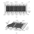
- FIG. 1 is a top view which shows a microlens array and a holder in the exposure apparatus which concerns on embodiment of this invention
- (b) is a partially expanded perspective view similarly.
- (A) is a figure which shows the permeation
- (b) is a top view which shows the exposure area
- (A) is a figure which shows the transmissive area
- (b) is a top view which similarly shows the exposure area
- FIG. 1 is a schematic view showing exposure by an exposure apparatus according to an embodiment of the present invention.
- FIG. 2A is a plan view showing a microlens array and a holder in the exposure apparatus according to the embodiment of the present invention.
- b) is a partially enlarged perspective view of the microlens array and the holder.
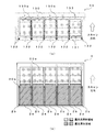
- FIG. 3A is a view showing a transmission area of exposure light in the microlens array in the exposure apparatus according to the first embodiment of the present invention
- FIG. 3B is an exposure area formed on the substrate.
- An exposure apparatus 1 forms an exposure pattern by scanning a substrate 2 having a positive resist material formed on the surface in a first direction, a light source 11 that emits exposure light, and a predetermined plurality of light sources 11.
- the substrate exposed by the exposure apparatus 1 of the present embodiment is a large glass substrate of, for example, 1500 mm ⁇ 1850 mm, and is manufactured by cutting out a plurality of individual substrates from the large glass substrate. That is, after the glass substrate 2 shown in FIG. 1 is exposed to a predetermined pattern shape of each individual substrate, a transparent electrode is formed on the surface through a development process and an etching process, and in a subsequent process, the glass substrate 2 is divided into each It becomes an individual board. Therefore, on the surface of the glass substrate 2 in the present embodiment, a transparent electrode material such as ITO (Indium-Tin-Oxido), for example, is formed over the entire region to be an individual substrate. A resist is formed.
- ITO Indium-Tin-Oxido
- the exposure light is irradiated onto the resist in a shape corresponding to the pattern of the mask 12, the resist in the region irradiated with the exposure light is exposed to the exposure light, and then removed by development and etching.
- the resist in the present invention is formed of a positive resist material that is a combination of a compound that generates an acid by photolysis and a binder resin that is decomposed by the generated acid and increases the solubility of the resist in a developer.
- the light source 11 in the present embodiment is a light source that emits laser light made of, for example, ultraviolet light, and is configured to continuously emit laser light during exposure.
- the light source 11 is moved in a first direction together with a microlens array, which will be described later, by a drive unit (not shown), thereby moving the exposure light irradiation position on the mask 12 in the first direction.
- the mask 12 has a pattern 12a corresponding to the shape of the transparent electrode formed on the individual substrate.
- the mask 12 is provided in a size corresponding to the glass substrate 2.
- the mask 12 has a pattern 12a having a shape corresponding to the circuit pattern for each individual substrate in a second direction orthogonal to the first direction in the scanning direction, in accordance with the number of individual substrates manufactured from the glass substrate 2. They are arranged so as to be aligned at a predetermined interval, and a plurality of rows are provided at a predetermined interval in the first direction in the scanning direction.
- the microlens array 13 is provided with a plurality of microlenses 131a.
- five microlens chips 131 are connected in the second direction.
- Each microlens chip 131 is connected to a frame-shaped holder 130 by a bracket 133 or the like and supported by the holder 130.
- Four microlenses 131a of the microlens chip 131 are arranged on the optical path of the exposure light, and when the exposure light transmitted through the mask 12 is incident, the pattern 12a is erected at the same magnification as the pattern 12a. Form an image.
- the holder 130 that supports the microlens array 13 is formed in a frame shape so as to support each microlens chip 131a at its edge. Therefore, as shown in FIG. 2, a light-shielding region through which exposure light is not transmitted is formed by the holder 130 between the microlens chips 131a.
- An opening 132 for transmitting exposure light is provided at a position that matches the position of the light shielding region between the microlens chips 131a. In the present embodiment, the opening 132 is provided at a position behind the microlens chip 131a in the scanning direction. Therefore, as shown in FIG.
- the holder 130 is provided with the exposure light transmitting opening 132 at a position aligned with the position of the light shielding region between the microlens chips 131a, so that the drive is performed in a state where the exposure light is emitted.
- the positive resist material in which the exposure light transmitted through the opening 132 is located in the region between the exposure patterns 2a (region 20b in FIG. 1). Is irradiated.
- substrate can be exposed reliably. Therefore, the positive resist material after the exposure can be surely removed in the subsequent etching process, and the circuit at the edge of each individual substrate can be prevented from being short-circuited.
- the exposure light transmitting openings 132 provided in the holder 130 are also provided at positions aligned with the outer edge portions of the chips 131 at both ends of the microlens array 13.
- the positive resist material at the edge of the substrate 2 can be exposed, and the positive resist material after the exposure is surely removed in a later etching step to short-circuit the circuit at the edge of the individual substrate, as in the above case. Can be prevented.
- a substrate 2 having a transparent electrode material formed on the surface and a positive resist material formed thereon is introduced into the exposure apparatus 1 and placed at the exposure start position.
- exposure light is emitted from the light source 11.
- the exposure light emitted from the light source 11 enters the mask 12 as shown in FIG.
- the irradiation region of the exposure light 3 on the mask 12 is provided so that the width in the second direction perpendicular to the scanning direction is slightly larger than the region to be a plurality of individual substrates arranged in the second direction.
- the mask 12 Since the mask 12 has a pattern 12a corresponding to the shape of the transparent electrode formed on the individual substrate, a part of the exposure light is blocked by the pattern 12a, and the transmitted light of the mask 12 is transmitted to the microlens array 13. Incident.
- the erecting equal-magnification image 20a of the pattern 12a is formed on the substrate 2 by each microlens 131a of the microlens array 13, and the positive resist material is exposed corresponding to the shape of the pattern 12a.
- the microlens array 13 is composed of five microlens chips 131 each provided with a plurality of microlenses 131a. It is connected. Since each microlens chip 131 has an edge supported by the holder 130, a light-blocking region through which exposure light is not transmitted is formed between the microlens chips 131.
- the holder 130 is aligned with the position of the light shielding region between the microlens chips 131a at a position behind the microlens chips 131a in the scanning direction.
- An opening 132 for transmitting exposure light is provided at a position where the exposure light is transmitted. Therefore, the exposure light transmitted through the opening 132 is also applied to the positive resist material (in the region 20 b) between the regions that become the individual substrates on the substrate 2.
- the exposure light irradiation position on the mask 12 is in the first direction.
- the microlens array 13 sequentially forms an image on the substrate 2 to form an exposure pattern 2a.
- the exposure light transmitted through the openings 132 is also transmitted between the exposure patterns 2a between the regions serving as the individual substrates so as to follow the pattern 12a formed on the substrate.
- the positive resist material located in the region (region 20b in FIG. 1) is irradiated to form an exposure region 2b.
- the opening 132 is provided at the end on the rear side in the scanning direction of the substrate 2 relative to the microlens chip 131a, when the exposure pattern 2a is formed, the opening in the scanning direction of the substrate 2 is performed. An unexposed area remains in the area between the exposed patterns 2a on the side.
- the light source 11 and the microlens 13 are further moved in the scanning direction with respect to the mask 12 while irradiating the exposure light, thereby leaving the unexposed portions remaining between the exposure patterns 2a.
- This area is also exposed.
- all the positive resist material between the regions to be the individual substrates can be surely exposed, and the positive resist material after the exposure can be surely removed in the subsequent etching process, and the edge of each individual substrate can be removed. Can be prevented from short-circuiting.
- the opening 132 for transmitting the exposure light is provided at a position aligned with the outer edge of the chip 131 at both ends of the microlens array 13, the positive resist material at the edge of the substrate 2 can also be exposed. This is preferable because the short circuit of the edge circuit of the individual substrate can be prevented.
- the exposure light transmitting opening 132 provided in the holder 130 is provided at a position on the rear side in the scanning direction with respect to the microlens chip 131a, but as shown in FIG.
- the opening 132 may be provided at a position ahead of the microlens chip 131a in the scanning direction.
- the pattern 12a formed in the region to be the individual substrate is formed so as to follow the exposure region 2b formed by the transmitted light through the opening 132 by the movement of the light source 11 and the microlens 13 with respect to the mask 12. It will be done. Therefore, the exposure start position is a position where the transmitted light of the opening 132 is irradiated to the rearmost end region between the regions that are the rearmost individual substrates in the scanning direction.
- an unexposed area does not remain between the exposure patterns 2a, but between the areas serving as individual substrates.
- the positive resist material can be reliably exposed.
- the opening 132 may be provided at both ends on the front side and the rear side in the scanning direction of the substrate 2 relative to the microlens chip 131a.
- the exposure start position can be aligned with the pattern 12a of the mask 12, and the stroke for moving the light source 11 and the microlens 13 relative to the mask 12 can be shortened as compared with the above case. .
- the mask 12 is provided in a size corresponding to the substrate 2, but in this embodiment, the substrate 2 is larger than in the first embodiment, and the substrate 2 in the second direction.
- the number of areas to be exposed is larger than the number of patterns of the mask 12 in the second direction. Therefore, the region to be exposed on the substrate 2 cannot be exposed by one scan.
- the exposure apparatus has a control device (not shown) that controls the position of the substrate 2 in the second direction.
- the exposure apparatus is configured such that the position of the stage on which the substrate 2 is placed is controlled by the control device, and the position of the substrate 2 can be moved in the second direction. Therefore, in this embodiment, when the exposure of the region corresponding to the number of patterns 12a formed on the mask 12 is completed, the control device temporarily stops the emission of exposure light from the light source 11. Then, as shown in FIG. 5, the control device moves the stage so that an erecting equal-magnification image of the pattern 12 a by the microlens array 13 is formed in an unexposed area of the substrate 2.
- the control device restarts the emission of exposure light from the light source 11, and moves the relative positions of the light source 11 and the microlens array 13 with respect to the mask 12 by the driving unit in the first direction, as in the first embodiment. Continuous exposure is performed. As shown in FIG. 5, if the scanning direction is opposite to that in the first embodiment, the light source 11 and the microlens array 13 are relative to the mask 12 while the emission of exposure light is stopped. This is preferable because there is no need to restore the position and the exposure tact can be shortened.
- the holder 130 forms a light-blocking region through which the exposure light is not transmitted between the five microlens chips 131, but the holder 130 has a microlens. Since the opening 132 for transmitting the exposure light is provided at a position aligned with the position of the light shielding area between the chips 131a, the exposure light transmitted through the opening 132 is between the areas that become individual substrates on the substrate 2 (area 20b). The positive resist material is also irradiated.
- the exposure light irradiation position on the mask 12 is in the first direction.
- the microlens array 13 sequentially forms an image on the substrate 2 to form an exposure pattern 2a.
- the positive resist material in which the exposure light transmitted through the opening 132 is located in the region between the exposure patterns 2a (see FIG. 5) between the regions serving as the individual substrates so as to follow the pattern 12a formed on the substrate.
- the region 20b) is irradiated.
- the position of the opening 132 in the first direction is a position on the front side in the scanning direction with respect to the microlens chip 131a, exposure similar to that in the modification of the first embodiment proceeds.
- the positive resist material between the regions to be the individual substrates can be reliably exposed, and the positive resist material after the exposure can be reliably removed in the subsequent etching step. It is possible to prevent the circuit at the edge of the individual substrate from being short-circuited. If the opening 132 for transmitting the exposure light is provided at a position aligned with the outer edge of the chip 131 at both ends of the microlens array 13, the positive resist material at the edge of the substrate 2 can also be exposed. This is preferable because the short circuit of the edge circuit of the individual substrate can be prevented.
- the opening 132 may be provided at both the front and rear ends in the scanning direction of the substrate 2 relative to the microlens chip 131a, and the exposure start position is the pattern 12a of the mask 12. Therefore, the stroke for moving the light source 11 and the microlens 13 relative to the mask 12 can be shortened.
- the substrate 2 is larger than in the second embodiment, and the number of regions to be exposed on the substrate 2 is larger than the number of patterns of the mask 12 in the second direction also in the first direction of the scan direction. It is comprised so that it may become. Therefore, the region to be exposed on the substrate 2 cannot be exposed by one scan.
- the control device in the exposure apparatus according to the second embodiment, is configured to be able to control the position of the substrate 2 also in the first direction. Therefore, in the present embodiment, when the exposure of the predetermined exposure target areas arranged in the second direction is completed, the control device temporarily stops the emission of the exposure light from the light source 11. Then, as shown in FIG. 6, the control apparatus moves the stage in the first direction so that an erecting equal-magnification image of the pattern 12 a by the microlens array 13 is formed in an unexposed area of the substrate 2. . Thereafter, the control device restarts the emission of the exposure light from the light source 11 and moves the relative positions of the light source 11 and the microlens array 13 with respect to the mask 12 in the first direction by the driving unit.
- a light-blocking region that does not transmit exposure light is formed between the five microlens chips 131, but the holder 130 has a microlens. Since the opening 132 for transmitting the exposure light is provided at a position aligned with the position of the light shielding area between the chips 131a, the exposure light transmitted through the opening 132 is between the areas that become individual substrates on the substrate 2 (area 20b). The positive resist material is also irradiated. Therefore, the continuous exposure similar to the first embodiment and the second embodiment can reliably expose the positive resist material between the regions to be the individual substrates, and the positive resist material after the exposure can be reliably used in the subsequent etching process.
- the opening 132 for transmitting the exposure light is provided at a position aligned with the outer edge of the chip 131 at both ends of the microlens array 13, the positive resist material at the edge of the substrate 2 can also be exposed. This is preferable because the short circuit of the edge circuit of the individual substrate can be prevented.
- the opening 132 may be provided at both the front and rear ends in the scanning direction of the substrate 2 relative to the microlens chip 131a, and the exposure start position is the pattern 12a of the mask 12. Therefore, the stroke for moving the light source 11 and the microlens 13 relative to the mask 12 can be shortened.
- an erecting equal-magnification image of the pattern 12a by the microlens array 13 is formed on the unexposed area of the substrate 2 by the control device.
- the stage in the second direction and performing exposure similar to the above it is possible to form an exposure region in which the short circuit of the edge circuit of the individual substrate is prevented.
- the present invention is useful as an exposure apparatus that can be used for manufacturing a small-sized liquid crystal display panel for mobile phones and the like, and can expose a mask pattern with high resolution.
Landscapes
- Physics & Mathematics (AREA)
- General Physics & Mathematics (AREA)
- Optics & Photonics (AREA)
- Exposure And Positioning Against Photoresist Photosensitive Materials (AREA)
- Lenses (AREA)
- Exposure Of Semiconductors, Excluding Electron Or Ion Beam Exposure (AREA)
Abstract
露光装置は、露光すべき複数個のパターンがスキャン方向に直交する方向に所定の間隔をおいて設けられたマスクに光源からの露光光を透過させ、マイクロレンズアレイの複数個のマイクロレンズによりパターンの正立等倍像を基板上に結像させる。マイクロレンズアレイは、マイクロレンズアレイチップが第2方向に接続されて構成されており、マイクロレンズアレイチップを支持する枠状のホルダには、マイクロレンズアレイチップ間の位置に整合する位置に露光光透過用の開口が設けられている。これにより、複数枚の個別基板となる領域に跨ってポジレジスト材料が形成された基板を露光することができる。
Description
本発明は、携帯電話用の液晶ディスプレイパネル等に使用されるガラス基板等を露光する露光装置に関し、特に、マスクと露光対象の基板との間に複数個のマイクロレンズが配置され、マスクのパターンを高い解像力で露光できる露光装置及びマイクロレンズアレイ構造体に関する。
従来、大型液晶ディスプレイパネル等に使用される例えばガラス基板等の露光には、レンズスキャニング方式、ミラープロジェクション方式及びプロキシミティ方式等の露光装置が使用されている。そして、大型のマスク上に形成されたパターンの透過光を、複数の投影光学系(マルチレンズ)に入射させて基板上に分割して結像させ、一度の露光により、基板上の複数の領域を露光することが行われている。このような露光方法は、3μm以上の解像力を必要とする基板の露光に採用されている。
しかしながら、例えば携帯電話用の液晶ディスプレイパネル等に使用されるガラス基板等、使用される基板が小さい場合においては、2μm以下と高い解像力が必要とされるため、上記のようなマルチレンズを使用した露光方法を採用することができない。よって、半導体用基板等の露光に使用されるステッパ方式の露光装置が使用されている(例えば、特許文献1及び2)。
ステッパ方式の露光装置においては、マスクに形成された各パターンの透過光は、縮小光学系に透過された後に、基板に照射される。従来、携帯電話用の液晶ディスプレイパネル等に使用されるガラス基板は、例えば1.5m角の大型の基板から製造され、露光の際には、1又は複数枚の個別のガラス基板となる領域ごとに複数回露光される。そして、複数回の露光により個別基板となる領域の全てが露光された基板は、分割されて、複数枚のガラス基板が製造される。
また、特許文献3には、マスクと基板との間にマイクロレンズアレイを配置し、マイクロレンズアレイにより、形成するパターンの解像力を高める技術も開示されている。即ち、特許文献3のように、露光すべきパターンが形成されたマスクを、各個別基板(パネル)に対応する大きさで設け、マイクロレンズの各マイクロレンズにより、露光すべきパターンを基板上に正立等倍像で結像させることにより、形成される露光パターンの解像力を高めることができる。
しかしながら、上記従来技術においては、以下のような問題点がある。特許文献1及び2に開示されたステッパ方式の露光装置においては、1又は複数枚の個別のガラス基板となる領域ごとに複数回露光を繰り返す必要があり、露光タクトが長くなるという問題点がある。
また、特許文献3のように、マイクロレンズアレイによる高解像力を得る場合においても、ステッパ方式の露光装置の場合と同様に、各個別基板ごとに、夫々対応する大きさで設けられたマスク及びマイクロレンズアレイによる露光を複数回繰り返し、基板上のポジレジスト材料を各個別基板となる領域ごとに露光することが行われている。よって、露光タクトが極めて長くなるという問題点がある。
この問題点を解決するためには、露光すべきパターンが複数枚の個別基板に対応して複数個設けられたマスクを使用することが考えられる。しかし、マスクパターンを結像するマイクロレンズアレイは、マスクの場合とは異なり、複数枚の個別基板に対応させて大型化することが難しい。そのため、マイクロレンズアレイとしては、各個別基板(パネル)の幅に合わせたマイクロレンズアレイチップを複数個接続したものを使用する必要がある。この際、各マイクロレンズアレイチップ間の領域は、ホルダにより支持された遮光領域となる。よって、この遮光領域に対応する個別基板(パネル)間の領域は露光されず、後のエッチング工程において、個別基板間の領域に電極材料が残存し、これにより、各個別基板の縁部の回路が短絡してしまうという問題点がある。
本発明はかかる問題点に鑑みてなされたものであって、複数枚の個別基板となる領域に跨ってポジレジスト材料が形成された基板を露光する露光装置において、個別基板となる領域間のポジレジスト材料を露光できる露光装置及び露光装置用マイクロレンズアレイ構造体を提供することを目的とする。
本発明に係る露光装置は、表面にポジレジスト材料が形成された基板を露光光で第1方向にスキャンして露光パターンを形成する露光装置において、露光光を出射する光源と、露光すべき複数個のパターンが前記第1方向に直交する第2方向に所定の間隔をおいて設けられ前記光源からの露光光が前記パターンを透過するマスクと、前記パターンの正立等倍像を前記基板上に結像させる複数個のマイクロレンズが配置されたマイクロレンズアレイと、このマイクロレンズアレイを支持する枠状のホルダと、前記マイクロレンズアレイ及び前記光源を前記マスクに対して相対的に前記第1方向に移動させる駆動部と、を有し、前記マイクロレンズアレイは、複数個のマイクロレンズが設けられたマイクロレンズアレイチップが前記第2方向に接続されて構成されており、前記ホルダには、前記マイクロレンズアレイの前記マイクロレンズアレイチップ間の位置に整合する位置に露光光透過用の開口が設けられていることを特徴とする。
本発明に係る露光装置用マイクロレンズアレイ構造体は、露光光を出射する光源と、露光すべき複数個のパターンが基板のスキャン方向の第1方向に直交する第2方向に所定の間隔をおいて設けられ前記光源からの露光光が前記パターンを透過するマスクと、前記パターンの正立等倍像を前記基板上に結像させる複数個のマイクロレンズが配置されたマイクロレンズアレイと、このマイクロレンズアレイを支持する枠状のホルダと、前記マイクロレンズアレイ及び前記光源を前記マスクに対して相対的に前記第1方向に移動させる駆動部と、を有し、表面にポジレジスト材料が形成された基板を露光光で前記第1方向にスキャンして露光パターンを形成する露光装置に使用されるマイクロレンズアレイ構造体において、前記マイクロレンズアレイは、複数個のマイクロレンズが設けられたマイクロレンズアレイチップが前記第2方向に接続されて構成されており、前記ホルダには、前記マイクロレンズアレイの前記マイクロレンズアレイチップ間の位置に整合する位置に露光光透過用の開口が設けられていることを特徴とする。
本発明において、例えば前記ホルダの開口は、前記基板のスキャン方向の前方及び後方の双方の端部に設けられているか、又は前記ホルダの開口は、前記基板のスキャン方向の前方及び後方の一方の端部に設けられている。また、前記ホルダには、更に、前記マイクロレンズアレイの両端部のチップの夫々外側の縁部に整合する位置にも露光光透過用の開口が設けられていることが好ましい。
上述の露光装置は、例えば更に、前記光源からの露光光の出射を停止した状態で、前記第2方向における前記基板の位置を制御する制御装置を有し、前記基板の前記第2方向における露光すべき領域の数が前記マスクの前記第2方向におけるパターン数よりも多い場合に、前記制御装置は、前記基板の前記パターン数に対応する領域が露光された後、露光光の出射を停止し、前記基板の未露光の領域に前記パターンの正立等倍像が結像されるように、前記基板を前記第2方向に移動させ、露光光の出射を再開させるように構成することができる。
また、例えば前記制御装置は、前記光源からの露光光の出射を停止した状態で、前記第1方向における前記基板の位置も制御可能に構成されており、前記基板の前記第1方向における露光すべき領域の数が前記マスクの前記第1方向におけるパターン数よりも多い場合に、前記基板の前記パターン数に対応する領域が露光された後、露光光の出射を停止し、前記基板の未露光の領域に前記パターンの正立等倍像が結像されるように、前記基板を前記第1方向に移動させ、露光光の出射を再開させるように構成してもよい。
本発明の露光装置は、マスクには露光すべき複数個のパターンが第1方向に所定の間隔をおいて設けられ、光源からの露光光は第1方向に並ぶ複数個のパターンに透過される。そして、パターンの正立等倍像を基板上に結像させるマイクロレンズアレイは、枠状のホルダにより支持されており、駆動部により、マイクロレンズアレイ及び光源をマスクに対して相対的に第1方向に移動させる。本発明においては、マイクロレンズアレイは、複数個のマイクロレンズが設けられたマイクロレンズアレイチップが第2方向に接続されて構成されているが、マイクロレンズアレイを支持するホルダには、マイクロレンズアレイチップ間の位置に整合する位置に露光光透過用の開口が設けられている。よって、光源から露光光を出射させた状態で、駆動部により、マイクロレンズアレイ及び光源をマスクに対して相対的に第1方向に移動させれば、基板上のパターン間の領域には、ホルダの開口を透過した露光光が照射され、個別基板となる領域間のポジレジスト材料を確実に露光できる。
以下、添付の図面を参照して本発明の実施形態について具体的に説明する。図1は、本発明の実施形態に係る露光装置による露光を示す模式図、図2(a)は本発明の実施形態に係る露光装置において、マイクロレンズアレイ及びホルダを示す平面図、図2(b)は同じくマイクロレンズアレイ及びホルダの一部拡大斜視図である。また、図3(a)は、本発明の第1実施形態に係る露光装置において、マイクロレンズアレイにおける露光光の透過領域を示す図、図3(b)は基板上に形成される露光領域を示す平面図である。本実施形態に係る露光装置1は、表面にポジレジスト材料が形成された基板2を第1方向にスキャンして露光パターンを形成するものであり、露光光を出射する光源11と、所定の複数個の露光パターンが形成されたマスク12と、マスク12の透過光が入射され各パターンの正立等倍像を基板上に結像させる複数個のマイクロレンズ131aが配置されたマイクロレンズアレイ13と、マイクロレンズアレイ13を支持するホルダ130とにより構成されている。
本実施形態の露光装置1により露光される基板は、例えば1500mm×1850mmの大型のガラス基板であり、この大型のガラス基板から複数枚の個別基板が切り出されて製造される。即ち、図1に示すガラス基板2は、各個別基板の所定のパターン形状に露光された後、現像工程及びエッチング工程を経て、表面に透明電極が形成され、後の工程において、分割されて各個別基板となる。よって、本実施形態におけるガラス基板2の表面には、個別基板となる領域の全域に、例えばITO(Indium-Tin-Oxido)等の透明電極材料が形成されており、透明電極材料の上には、レジストが形成されている。本発明においては、露光光をマスク12のパターンに対応する形状でレジストに照射し、露光光が照射された領域のレジストを露光光により感光させて、その後、現像及びエッチングを施すことにより除去する。よって、本発明におけるレジストは、光分解により酸を発生する化合物と、発生した酸により分解されて現像液中におけるレジストの溶解性を高めるバインダー樹脂とを組み合わせたポジレジスト材料により形成されている。
本実施形態における光源11は、例えば紫外光からなるレーザ光を出射する光源であり、露光の際には、レーザ光を連続的に出射するように構成されている。光源11は、図示しない駆動部により、後述するマイクロレンズアレイと共に第1方向に移動され、これにより、マスク12に対する露光光の照射位置を第1方向に移動させるように構成されている。
マスク12は、個別基板に形成する透明電極の形状に対応するパターン12aが形成されたものである。本実施形態においては、図1に示すように、マスク12は、ガラス基板2に対応する大きさで設けられている。そして、マスク12には、ガラス基板2から製造される個別基板の枚数に合わせて、各個別基板用の回路パターンに対応する形状のパターン12aがスキャン方向の第1方向に直交する第2方向に所定間隔をおいて整列するように設けられており、また、スキャン方向の第1方向に複数行が所定間隔をおいて設けられている。
図2に示すように、マイクロレンズアレイ13は、複数個のマイクロレンズ131aが設けられたものであり、本実施形態においては、5枚のマイクロレンズチップ131が、第2方向に接続されて構成されている。そして、各マイクロレンズチップ131は、ブラケット133等により枠状のホルダ130に接続されてホルダ130に支持されている。マイクロレンズチップ131の各マイクロレンズ131aは、露光光の光路上に4個ずつ配列されており、マスク12を透過した露光光が入射されることにより、基板2上にパターン12aの正立等倍像を結像させる。
マイクロレンズアレイ13を支持するホルダ130は、各マイクロレンズチップ131aをその縁部で支持するように枠状に形成されている。よって、図2に示すように、マイクロレンズチップ131a間には、ホルダ130により、露光光が透過されない遮光領域が形成されている。そして、このマイクロレンズチップ131a間の遮光領域の位置に整合する位置に露光光透過用の開口132が設けられている。本実施形態においては、開口132は、マイクロレンズチップ131aよりもスキャン方向の後方側の位置に設けられている。よって、図1に示すように、光源11から露光光3を照射しながら、駆動部により光源11及びマイクロレンズ13がマスク12に対して相対的に第1方向に移動されると、マスク12及びマイクロレンズ13の透過光により、基板2上の個別基板となる領域には、マスク12のパターン12aの正立等倍像20aが結像し、基板上のポジレジスト材料が、パターン12aの形状に対応して露光され、露光パターン2aが形成されていく。このとき、露光パターン2a間の領域は、ホルダ130による遮光により、露光光が照射されない部分となる。本実施形態においては、ホルダ130には、マイクロレンズチップ131a間の遮光領域の位置に整合する位置に露光光透過用の開口132が設けられているので、露光光を出射させた状態で、駆動部により、光源11及びマイクロレンズ13をマスク12に対して第1方向に移動させると、開口132を透過した露光光が露光パターン2a間の領域に位置するポジレジスト材料(図1における領域20b)に照射される。これにより、個別基板となる領域間のポジレジスト材料を確実に露光できる。よって、この露光後のポジレジスト材料を、後のエッチング工程において、確実に除去することができ、各個別基板の縁部の回路が短絡することを防止できる。
本実施形態においては、ホルダ130に設けられた露光光透過用の開口132は、マイクロレンズアレイ13の両端部のチップ131の夫々外側の縁部に整合する位置にも設けられており、これにより、基板2の縁部のポジレジスト材料を露光でき、上記の場合と同様に、露光後のポジレジスト材料を、後のエッチング工程において、確実に除去して個別基板の縁部の回路が短絡することを防止できる。
次に本実施形態の露光装置の動作について説明する。本実施形態においては、先ず、表面に透明電極材料が形成され、更にその上にポジレジスト材料が形成された基板2を、露光装置1内に導入し、露光開始位置に設置する。
そして、光源11から露光光を出射させる。光源11から出射された露光光は、図1に示すように、マスク12に入射される。露光光3のマスク12における照射領域は、スキャン方向に垂直の第2方向における幅が、第2方向に並ぶ複数の個別基板となる領域よりも若干大きくなるように設けられている。
マスク12には、個別基板に形成する透明電極の形状に対応するパターン12aが形成されているため、このパターン12aにより露光光の一部が遮光され、マスク12の透過光がマイクロレンズアレイ13に入射される。
そして、マイクロレンズアレイ13の各マイクロレンズ131aにより、パターン12aの正立等倍像20aが基板2上に結像され、ポジレジスト材料がパターン12aの形状に対応して露光される。本実施形態においては、図2に示すように、マイクロレンズアレイ13は、夫々複数個のマイクロレンズ131aが設けられた5枚のマイクロレンズチップ131により構成されており、相互間が第2方向に接続されている。そして、各マイクロレンズチップ131は、ホルダ130により、縁部が支持されているため、マイクロレンズチップ131間には、露光光が透過されない遮光領域が形成されている。
しかし、本実施形態においては、図3(a)に示すように、ホルダ130には、マイクロレンズチップ131aよりもスキャン方向の後方側の位置において、マイクロレンズチップ131a間の遮光領域の位置に整合する位置に、露光光透過用の開口132が設けられている。よって、開口132を透過した露光光が、基板2上の個別基板となる領域間の(領域20bの)ポジレジスト材料にも照射される。
この状態で、露光光の出射を継続したまま、駆動部により、光源11及びマイクロレンズ13をマスク12に対して第1方向に移動させると、マスク12における露光光の照射位置が第1方向に移動する。よって、パターン12aが第1方向にスキャンされながら、マイクロレンズアレイ13により基板2上に順次結像されていき、露光パターン2aが形成されていく。
このとき、図3(b)に示すように、基板上に形成されていくパターン12aに追従するように、個別基板となる領域間にも、開口132を透過した露光光が露光パターン2a間の領域に位置するポジレジスト材料(図1における領域20b)に照射され、露光領域2bが形成されていく。本実施形態においては、開口132は、マイクロレンズチップ131aよりも基板2のスキャン方向における後方側の端部に設けられているため、露光パターン2aが形成されたときに、基板2のスキャン方向前方側における露光パターン2a間の領域には、未露光の領域が残る。しかし、露光パターン2aの形成が完了した後、露光光を照射しながら、光源11及びマイクロレンズ13を、マスク12に対して更にスキャン方向に移動させることにより、露光パターン2a間に残った未露光の領域も露光される。これにより、個別基板となる領域間の全てのポジレジスト材料を確実に露光でき、この露光後のポジレジスト材料を、後のエッチング工程において、確実に除去することができ、各個別基板の縁部の回路が短絡することを防止できる。
そして、露光光透過用の開口132をマイクロレンズアレイ13の両端部のチップ131の夫々外側の縁部に整合する位置に設ければ、基板2の縁部のポジレジスト材料も露光でき、この部分における個別基板の縁部回路の短絡も防止できるので好ましい。
なお、本実施形態においては、ホルダ130に設けられた露光光透過用の開口132は、マイクロレンズチップ131aよりもスキャン方向の後方側の位置に設けられているが、図4に示すように、開口132は、マイクロレンズチップ131aよりもスキャン方向の前方側の位置に設けられていてもよい。この場合には、個別基板となる領域に形成されるパターン12aは、マスク12に対する光源11及びマイクロレンズ13の移動により、開口132の透過光により形成される露光領域2bに追従するように、形成されていく。よって、露光の開始位置は、スキャン方向における最も後方の個別基板となる領域間において、その最も後端側の領域に開口132の透過光が照射される位置とする。これにより、開口132をマイクロレンズチップ131aよりもスキャン方向における後方側の端部に設けた場合と同様に、露光パターン2a間に未露光の領域が残ることはなく、個別基板となる領域間のポジレジスト材料を確実に露光することができる。
また、開口132は、マイクロレンズチップ131aよりも基板2のスキャン方向の前方側及び後方側の双方の端部に設けてもよい。この場合には、露光の開始位置をマスク12のパターン12aに合わせることができ、上記の場合に比して、光源11及びマイクロレンズ13をマスク12に対して相対的に移動させるストロークを短くできる。
次に、本発明の第2実施形態に係る露光装置について説明する。第1実施形態においては、マスク12は基板2に対応する大きさで設けられていたが、本実施形態においては、第1実施形態の場合よりも基板2が大きく、第2方向において、基板2の露光すべき領域の数が第2方向におけるマスク12のパターン数よりも多くなるように構成されている。よって、基板2の露光すべき領域を1回のスキャンにより露光することはできない。
本実施形態においては、露光装置は、第2方向における基板2の位置を制御する制御装置(図示せず)を有している。例えば、露光装置は、基板2が載置されたステージの位置が制御装置により制御されており、基板2の位置を第2方向に移動可能に構成されている。よって、本実施形態においては、マスク12に形成されたパターン12aの数に対応する領域の露光が終了したら、制御装置は、光源11からの露光光の出射を一旦停止する。そして、制御装置は、図5に示すように、基板2の未露光の領域にマイクロレンズアレイ13によるパターン12aの正立等倍像が結像されるように、ステージを移動させる。その後、制御装置は、光源11からの露光光の出射を再開させ、駆動部によりマスク12に対する光源11及びマイクロレンズアレイ13の相対的位置を第1方向に移動させながら、第1実施形態と同様の連続露光を行う。なお、スキャン方向は、図5に示すように、第1実施形態の場合と逆方向にすれば、露光光の出射を停止している間にマスク12に対する光源11及びマイクロレンズアレイ13の相対的位置を元に戻す必要がなく、露光タクトを短縮できるので好ましい。
本実施形態においても、第1実施形態と同様に、ホルダ130により、5枚のマイクロレンズチップ131間には、露光光が透過されない遮光領域が形成されているが、ホルダ130には、マイクロレンズチップ131a間の遮光領域の位置に整合する位置に露光光透過用の開口132が設けられているので、開口132を透過した露光光が、基板2上の個別基板となる領域間の(領域20bの)ポジレジスト材料にも照射される。
この状態で、露光光の出射を継続したまま、駆動部により、光源11及びマイクロレンズ13をマスク12に対して第1方向に移動させると、マスク12における露光光の照射位置が第1方向に移動し、パターン12aが第1方向にスキャンされながら、マイクロレンズアレイ13により基板2上に順次結像されていき、露光パターン2aが形成されていく。このとき、基板上に形成されていくパターン12aに追従するように、個別基板となる領域間にも、開口132を透過した露光光が露光パターン2a間の領域に位置するポジレジスト材料(図5における領域20b)に照射されていく。但し、本実施形態においては、第1方向における開口132の位置は、マイクロレンズチップ131aよりもスキャン方向の前方側の位置となるため、第1実施形態の変形例と同様の露光が進行する。
このように、本実施形態においても、個別基板となる領域間のポジレジスト材料を確実に露光でき、この露光後のポジレジスト材料を、後のエッチング工程において、確実に除去することができ、各個別基板の縁部の回路が短絡することを防止できる。そして、露光光透過用の開口132をマイクロレンズアレイ13の両端部のチップ131の夫々外側の縁部に整合する位置に設ければ、基板2の縁部のポジレジスト材料も露光でき、この部分における個別基板の縁部回路の短絡も防止できるので好ましい。
なお、本実施形態においても、開口132は、マイクロレンズチップ131aよりも基板2のスキャン方向の前方側及び後方側の双方の端部に設けてもよく、露光の開始位置をマスク12のパターン12aに合わせることにより、光源11及びマイクロレンズ13をマスク12に対して相対的に移動させるストロークを短くできる。
次に、本発明の第3実施形態に係る露光装置について説明する。本実施形態においては、第2実施形態の場合よりも基板2が大きく、スキャン方向の第1方向においても、基板2の露光すべき領域の数が第2方向におけるマスク12のパターン数よりも多くなるように構成されている。よって、基板2の露光すべき領域を1回のスキャンにより露光することはできない。
本実施形態においては、第2実施形態に係る露光装置において、制御装置は、基板2の位置を第1方向にも制御可能に構成されている。よって、本実施形態においては、第2方向に並ぶ所定の露光対象領域の露光が終了したら、制御装置は、光源11からの露光光の出射を一旦停止する。そして、制御装置は、図6に示すように、基板2の未露光の領域にマイクロレンズアレイ13によるパターン12aの正立等倍像が結像されるように、ステージを第1方向に移動させる。その後、制御装置は、光源11からの露光光の出射を再開させ、駆動部によりマスク12に対する光源11及びマイクロレンズアレイ13の相対的位置を第1方向に移動させながら、第1実施形態及び第2実施形態と同様の連続露光を行う。なお、スキャン方向は、図6に示すように、第1実施形態の場合と同一方向にすれば、露光光の出射を停止している間にマスク12に対する光源11及びマイクロレンズアレイ13の相対的位置を元に戻す必要がなく、露光タクトを短縮できるので好ましい。
本実施形態においても、第1実施形態及び第2実施形態と同様に、5枚のマイクロレンズチップ131間には、露光光が透過されない遮光領域が形成されているがホルダ130には、マイクロレンズチップ131a間の遮光領域の位置に整合する位置に露光光透過用の開口132が設けられているので、開口132を透過した露光光が、基板2上の個別基板となる領域間の(領域20bの)ポジレジスト材料にも照射される。よって、第1実施形態及び第2実施形態と同様の連続露光により、個別基板となる領域間のポジレジスト材料を確実に露光でき、この露光後のポジレジスト材料を、後のエッチング工程において、確実に除去することができ、各個別基板の縁部の回路が短絡することを防止できる。そして、露光光透過用の開口132をマイクロレンズアレイ13の両端部のチップ131の夫々外側の縁部に整合する位置に設ければ、基板2の縁部のポジレジスト材料も露光でき、この部分における個別基板の縁部回路の短絡も防止できるので好ましい。
なお、本実施形態においても、開口132は、マイクロレンズチップ131aよりも基板2のスキャン方向の前方側及び後方側の双方の端部に設けてもよく、露光の開始位置をマスク12のパターン12aに合わせることにより、光源11及びマイクロレンズ13をマスク12に対して相対的に移動させるストロークを短くできる。
なお、図6に2点鎖線で示す領域については、上記露光が終了した後、制御装置により、基板2の未露光の領域にマイクロレンズアレイ13によるパターン12aの正立等倍像が結像されるように、ステージを第2方向に移動させ、上記と同様の露光を行うことにより、個別基板の縁部回路の短絡を防止した露光領域を形成することができる。
以上説明した露光装置において、例えば図7に示すように、光源11を4台設け、夫々の光源11に対応させて、マスク12及びマイクロレンズアレイ13を設ければ、より大型の基板2を露光することができ、露光タクトを短縮できるという効果を得ることができる。
本発明は、携帯電話用の小型液晶ディスプレイパネル等の製造に使用され、マスクのパターンを高解像力で露光できる露光装置として、有益である。
1:露光装置、11:光源、12:マスク、13:マイクロレンズアレイ、2:基板
Claims (10)
- 表面にポジレジスト材料が形成された基板を露光光で第1方向にスキャンして露光パターンを形成する露光装置において、
露光光を出射する光源と、
露光すべき複数個のパターンが前記第1方向に直交する第2方向に所定の間隔をおいて設けられ前記光源からの露光光が前記パターンを透過するマスクと、
前記パターンの正立等倍像を前記基板上に結像させる複数個のマイクロレンズが配置されたマイクロレンズアレイと、
このマイクロレンズアレイを支持する枠状のホルダと、
前記マイクロレンズアレイ及び前記光源を前記マスクに対して相対的に前記第1方向に移動させる駆動部と、
を有し、
前記マイクロレンズアレイは、複数個のマイクロレンズが設けられたマイクロレンズアレイチップが前記第2方向に接続されて構成されており、
前記ホルダには、前記マイクロレンズアレイの前記マイクロレンズアレイチップ間の位置に整合する位置に露光光透過用の開口が設けられていることを特徴とする露光装置。 - 前記ホルダの開口は、前記基板のスキャン方向の前方及び後方の双方の端部に設けられていることを特徴とする請求項1に記載の露光装置。
- 前記ホルダの開口は、前記基板のスキャン方向の前方及び後方の一方の端部に設けられていることを特徴とする請求項1に記載の露光装置。
- 前記ホルダには、更に、前記マイクロレンズアレイの両端部のチップの夫々外側の縁部に整合する位置にも露光光透過用の開口が設けられていることを特徴とする請求項1乃至3のいずれか1項に記載の露光装置。
- 更に、前記光源からの露光光の出射を停止した状態で、前記第2方向における前記基板の位置を制御する制御装置を有し、
前記基板の前記第2方向における露光すべき領域の数が前記マスクの前記第2方向におけるパターン数よりも多い場合に、前記制御装置は、前記基板の前記パターン数に対応する領域が露光された後、露光光の出射を停止し、前記基板の未露光の領域に前記パターンの正立等倍像が結像されるように、前記基板を前記第2方向に移動させ、露光光の出射を再開させることを特徴とする請求項1乃至4のいずれか1項に記載の露光装置。 - 前記制御装置は、前記光源からの露光光の出射を停止した状態で、前記第1方向における前記基板の位置も制御可能に構成されており、前記基板の前記第1方向における露光すべき領域の数が前記マスクの前記第1方向におけるパターン数よりも多い場合に、前記基板の前記パターン数に対応する領域が露光された後、露光光の出射を停止し、前記基板の未露光の領域に前記パターンの正立等倍像が結像されるように、前記基板を前記第1方向に移動させ、露光光の出射を再開させることを特徴とする請求項5に記載の露光装置。
- 露光光を出射する光源と、露光すべき複数個のパターンが基板のスキャン方向の第1方向に直交する第2方向に所定の間隔をおいて設けられ前記光源からの露光光が前記パターンを透過するマスクと、前記パターンの正立等倍像を前記基板上に結像させる複数個のマイクロレンズが配置されたマイクロレンズアレイと、このマイクロレンズアレイを支持する枠状のホルダと、前記マイクロレンズアレイ及び前記光源を前記マスクに対して相対的に前記第1方向に移動させる駆動部と、を有し、表面にポジレジスト材料が形成された基板を露光光で前記第1方向にスキャンして露光パターンを形成する露光装置に使用されるマイクロレンズアレイ構造体において、
前記マイクロレンズアレイは、複数個のマイクロレンズが設けられたマイクロレンズアレイチップが前記第2方向に接続されて構成されており、前記ホルダには、前記マイクロレンズアレイの前記マイクロレンズアレイチップ間の位置に整合する位置に露光光透過用の開口が設けられていることを特徴とする露光装置用マイクロレンズアレイ構造体。 - 前記ホルダの開口は、前記基板のスキャン方向の前方及び後方の双方の端部に設けられていることを特徴とする請求項7に記載のマイクロレンズアレイ構造体。
- 前記ホルダの開口は、前記基板のスキャン方向の前方及び後方の一方の端部に設けられていることを特徴とする請求項7に記載のマイクロレンズアレイ構造体。
- 前記ホルダには、更に、前記マイクロレンズアレイの両端部のチップの夫々外側の縁部に整合する位置にも露光光透過用の開口が設けられていることを特徴とする請求項7乃至9のいずれか1項に記載の露光装置用マイクロレンズアレイ構造体。
Priority Applications (2)
| Application Number | Priority Date | Filing Date | Title |
|---|---|---|---|
| CN201280011228.XA CN103392150B (zh) | 2011-03-02 | 2012-02-02 | 曝光装置以及微透镜阵列结构体 |
| KR1020137026000A KR20140022822A (ko) | 2011-03-02 | 2012-02-02 | 노광 장치 및 마이크로 렌즈 어레이 구조체 |
Applications Claiming Priority (2)
| Application Number | Priority Date | Filing Date | Title |
|---|---|---|---|
| JP2011045578A JP5747305B2 (ja) | 2011-03-02 | 2011-03-02 | 露光装置及びマイクロレンズアレイ構造体 |
| JP2011-045578 | 2011-03-02 |
Publications (1)
| Publication Number | Publication Date |
|---|---|
| WO2012117802A1 true WO2012117802A1 (ja) | 2012-09-07 |
Family
ID=46757742
Family Applications (1)
| Application Number | Title | Priority Date | Filing Date |
|---|---|---|---|
| PCT/JP2012/052379 Ceased WO2012117802A1 (ja) | 2011-03-02 | 2012-02-02 | 露光装置及びマイクロレンズアレイ構造体 |
Country Status (5)
| Country | Link |
|---|---|
| JP (1) | JP5747305B2 (ja) |
| KR (1) | KR20140022822A (ja) |
| CN (1) | CN103392150B (ja) |
| TW (1) | TWI529443B (ja) |
| WO (1) | WO2012117802A1 (ja) |
Citations (6)
| Publication number | Priority date | Publication date | Assignee | Title |
|---|---|---|---|---|
| JPH0855783A (ja) * | 1994-08-16 | 1996-02-27 | Nikon Corp | 露光装置 |
| JPH09244255A (ja) * | 1996-03-13 | 1997-09-19 | Nikon Corp | 液晶用露光装置 |
| JPH09244254A (ja) * | 1996-03-13 | 1997-09-19 | Nikon Corp | 液晶用露光装置 |
| JP2000058422A (ja) * | 1998-08-11 | 2000-02-25 | Nikon Corp | 露光装置 |
| JP2007281317A (ja) * | 2006-04-11 | 2007-10-25 | V Technology Co Ltd | 露光装置 |
| JP2009204982A (ja) * | 2008-02-28 | 2009-09-10 | Dainippon Screen Mfg Co Ltd | パターン描画装置及びパターン描画方法 |
Family Cites Families (7)
| Publication number | Priority date | Publication date | Assignee | Title |
|---|---|---|---|---|
| JP2000294501A (ja) * | 1999-04-09 | 2000-10-20 | Nikon Corp | 周辺露光装置及び方法 |
| JP2000299273A (ja) * | 1999-04-14 | 2000-10-24 | Nikon Corp | 周辺露光装置及び方法 |
| CN1282904C (zh) * | 2003-12-27 | 2006-11-01 | 上海华虹(集团)有限公司 | 一次扫描两个普通曝光区域的曝光方法 |
| KR100638107B1 (ko) * | 2005-06-09 | 2006-10-24 | 연세대학교 산학협력단 | 이머젼 박막층을 구비하는 광변조 미세개구 어레이 장치 및이를 이용한 고속 미세패턴 기록시스템 |
| JP4491447B2 (ja) * | 2005-11-04 | 2010-06-30 | 株式会社オーク製作所 | レーザビーム・紫外線照射周辺露光装置およびその方法 |
| KR100911020B1 (ko) * | 2007-10-29 | 2009-08-05 | 삼성전기주식회사 | 마스크, 이를 구비한 노광장치 및 전사방법 |
| CN101936504B (zh) * | 2010-09-03 | 2012-05-23 | 浙江大学 | 一种用于光刻多极照明的自由曲面微透镜阵列装置 |
-
2011
- 2011-03-02 JP JP2011045578A patent/JP5747305B2/ja not_active Expired - Fee Related
-
2012
- 2012-02-02 KR KR1020137026000A patent/KR20140022822A/ko not_active Withdrawn
- 2012-02-02 CN CN201280011228.XA patent/CN103392150B/zh not_active Expired - Fee Related
- 2012-02-02 WO PCT/JP2012/052379 patent/WO2012117802A1/ja not_active Ceased
- 2012-02-21 TW TW101105667A patent/TWI529443B/zh not_active IP Right Cessation
Patent Citations (6)
| Publication number | Priority date | Publication date | Assignee | Title |
|---|---|---|---|---|
| JPH0855783A (ja) * | 1994-08-16 | 1996-02-27 | Nikon Corp | 露光装置 |
| JPH09244255A (ja) * | 1996-03-13 | 1997-09-19 | Nikon Corp | 液晶用露光装置 |
| JPH09244254A (ja) * | 1996-03-13 | 1997-09-19 | Nikon Corp | 液晶用露光装置 |
| JP2000058422A (ja) * | 1998-08-11 | 2000-02-25 | Nikon Corp | 露光装置 |
| JP2007281317A (ja) * | 2006-04-11 | 2007-10-25 | V Technology Co Ltd | 露光装置 |
| JP2009204982A (ja) * | 2008-02-28 | 2009-09-10 | Dainippon Screen Mfg Co Ltd | パターン描画装置及びパターン描画方法 |
Also Published As
| Publication number | Publication date |
|---|---|
| JP5747305B2 (ja) | 2015-07-15 |
| JP2012181453A (ja) | 2012-09-20 |
| KR20140022822A (ko) | 2014-02-25 |
| TW201243420A (en) | 2012-11-01 |
| CN103392150A (zh) | 2013-11-13 |
| TWI529443B (zh) | 2016-04-11 |
| CN103392150B (zh) | 2015-09-23 |
Similar Documents
| Publication | Publication Date | Title |
|---|---|---|
| US9122171B2 (en) | Exposure apparatus | |
| KR100859400B1 (ko) | 광 조사 장치 | |
| US8697319B2 (en) | Exposure method, color filter manufacturing method, and exposure device | |
| US20220163894A1 (en) | System and method for double-sided digital lithography or exposure | |
| JP2003255552A (ja) | レーザ照射装置並びに走査レーザ光を用いた露光方法及び走査レーザ光を用いたカラーフィルタの製造方法 | |
| KR101977801B1 (ko) | 레티클 형성용 노광 장치 및 이를 이용한 레티클 제조 방법 | |
| JP5825470B2 (ja) | 露光装置及び遮光板 | |
| US8072580B2 (en) | Maskless exposure apparatus and method of manufacturing substrate for display using the same | |
| KR101949389B1 (ko) | 마스크리스 노광장치를 이용한 패턴 형성 방법 | |
| JP2010161246A (ja) | 伝送光学系、照明光学系、露光装置、露光方法、およびデバイス製造方法 | |
| JP5747305B2 (ja) | 露光装置及びマイクロレンズアレイ構造体 | |
| JP7427352B2 (ja) | 露光装置 | |
| KR102020934B1 (ko) | 마스크리스 노광 장치의 얼라인 방법 | |
| JP5704535B2 (ja) | マイクロレンズアレイを使用した露光装置 | |
| JP5253037B2 (ja) | 露光装置、露光方法、及び表示用パネル基板の製造方法 | |
| KR100958574B1 (ko) | 액정표시장치의 제조장치 및 방법 | |
| JP2010122619A (ja) | パターン描画装置、パターン描画方法及びパターン描画用のマスク | |
| KR101390512B1 (ko) | 개선된 패턴 형성용 노광 광원, 노광 장치, 노광 시스템, 및 노광 방법 | |
| JP2009117516A (ja) | パターン描画装置 | |
| KR20050011378A (ko) | 액정표시장치 노광 방법 | |
| KR20130123405A (ko) | 노광 장치 | |
| JP2007199116A (ja) | パターン形成方法、電子ディスプレイ用構造物及びディスプレイ | |
| KR20100093219A (ko) | 기판 패턴 노광 장치 |
Legal Events
| Date | Code | Title | Description |
|---|---|---|---|
| 121 | Ep: the epo has been informed by wipo that ep was designated in this application |
Ref document number: 12752277 Country of ref document: EP Kind code of ref document: A1 |
|
| NENP | Non-entry into the national phase |
Ref country code: DE |
|
| ENP | Entry into the national phase |
Ref document number: 20137026000 Country of ref document: KR Kind code of ref document: A |
|
| 122 | Ep: pct application non-entry in european phase |
Ref document number: 12752277 Country of ref document: EP Kind code of ref document: A1 |