WO2012114958A1 - タッチパネル母基板、該タッチパネル母基板から切り出されたタッチパネルおよびその製造方法 - Google Patents
タッチパネル母基板、該タッチパネル母基板から切り出されたタッチパネルおよびその製造方法 Download PDFInfo
- Publication number
- WO2012114958A1 WO2012114958A1 PCT/JP2012/053553 JP2012053553W WO2012114958A1 WO 2012114958 A1 WO2012114958 A1 WO 2012114958A1 JP 2012053553 W JP2012053553 W JP 2012053553W WO 2012114958 A1 WO2012114958 A1 WO 2012114958A1
- Authority
- WO
- WIPO (PCT)
- Prior art keywords
- touch panel
- conductive pattern
- electrode
- mother board
- electrodes
- Prior art date
- Legal status (The legal status is an assumption and is not a legal conclusion. Google has not performed a legal analysis and makes no representation as to the accuracy of the status listed.)
- Ceased
Links
Images




Classifications
-
- G—PHYSICS
- G06—COMPUTING OR CALCULATING; COUNTING
- G06F—ELECTRIC DIGITAL DATA PROCESSING
- G06F3/00—Input arrangements for transferring data to be processed into a form capable of being handled by the computer; Output arrangements for transferring data from processing unit to output unit, e.g. interface arrangements
- G06F3/01—Input arrangements or combined input and output arrangements for interaction between user and computer
- G06F3/03—Arrangements for converting the position or the displacement of a member into a coded form
- G06F3/041—Digitisers, e.g. for touch screens or touch pads, characterised by the transducing means
- G06F3/044—Digitisers, e.g. for touch screens or touch pads, characterised by the transducing means by capacitive means
-
- G—PHYSICS
- G06—COMPUTING OR CALCULATING; COUNTING
- G06F—ELECTRIC DIGITAL DATA PROCESSING
- G06F3/00—Input arrangements for transferring data to be processed into a form capable of being handled by the computer; Output arrangements for transferring data from processing unit to output unit, e.g. interface arrangements
- G06F3/01—Input arrangements or combined input and output arrangements for interaction between user and computer
- G06F3/03—Arrangements for converting the position or the displacement of a member into a coded form
- G06F3/041—Digitisers, e.g. for touch screens or touch pads, characterised by the transducing means
- G06F3/044—Digitisers, e.g. for touch screens or touch pads, characterised by the transducing means by capacitive means
- G06F3/0446—Digitisers, e.g. for touch screens or touch pads, characterised by the transducing means by capacitive means using a grid-like structure of electrodes in at least two directions, e.g. using row and column electrodes
-
- G—PHYSICS
- G06—COMPUTING OR CALCULATING; COUNTING
- G06F—ELECTRIC DIGITAL DATA PROCESSING
- G06F3/00—Input arrangements for transferring data to be processed into a form capable of being handled by the computer; Output arrangements for transferring data from processing unit to output unit, e.g. interface arrangements
- G06F3/01—Input arrangements or combined input and output arrangements for interaction between user and computer
- G06F3/03—Arrangements for converting the position or the displacement of a member into a coded form
- G06F3/041—Digitisers, e.g. for touch screens or touch pads, characterised by the transducing means
- G06F3/0416—Control or interface arrangements specially adapted for digitisers
- G06F3/04164—Connections between sensors and controllers, e.g. routing lines between electrodes and connection pads
-
- G—PHYSICS
- G06—COMPUTING OR CALCULATING; COUNTING
- G06F—ELECTRIC DIGITAL DATA PROCESSING
- G06F3/00—Input arrangements for transferring data to be processed into a form capable of being handled by the computer; Output arrangements for transferring data from processing unit to output unit, e.g. interface arrangements
- G06F3/01—Input arrangements or combined input and output arrangements for interaction between user and computer
- G06F3/03—Arrangements for converting the position or the displacement of a member into a coded form
- G06F3/041—Digitisers, e.g. for touch screens or touch pads, characterised by the transducing means
- G06F3/044—Digitisers, e.g. for touch screens or touch pads, characterised by the transducing means by capacitive means
- G06F3/0443—Digitisers, e.g. for touch screens or touch pads, characterised by the transducing means by capacitive means using a single layer of sensing electrodes
-
- G—PHYSICS
- G06—COMPUTING OR CALCULATING; COUNTING
- G06F—ELECTRIC DIGITAL DATA PROCESSING
- G06F2203/00—Indexing scheme relating to G06F3/00 - G06F3/048
- G06F2203/041—Indexing scheme relating to G06F3/041 - G06F3/045
- G06F2203/04103—Manufacturing, i.e. details related to manufacturing processes specially suited for touch sensitive devices
-
- G—PHYSICS
- G06—COMPUTING OR CALCULATING; COUNTING
- G06F—ELECTRIC DIGITAL DATA PROCESSING
- G06F2203/00—Indexing scheme relating to G06F3/00 - G06F3/048
- G06F2203/041—Indexing scheme relating to G06F3/041 - G06F3/045
- G06F2203/04111—Cross over in capacitive digitiser, i.e. details of structures for connecting electrodes of the sensing pattern where the connections cross each other, e.g. bridge structures comprising an insulating layer, or vias through substrate
Definitions
- the present invention relates to a touch panel mother board, a touch panel cut out from the touch panel mother board, and a manufacturing method thereof.
- a touch panel capable of detecting a position touched by a pen or a finger on the operation surface, that is, a touch position.
- Such a touch panel has a plurality of first electrodes and second electrodes extending in directions intersecting each other on a substrate, as disclosed in, for example, Japanese Patent Application Laid-Open No. 2010-160670.
- the touch panel manufacturing process there is a process of cutting and separating the touch panel from the touch panel mother board after arranging a plurality of touch panels on a large substrate (touch panel mother board) to form a pattern.
- this process there is a problem that static electricity is likely to be generated due to transportation, film surface protection treatment, and the like, and pattern destruction due to electrostatic breakdown occurs, resulting in a decrease in product yield.
- a configuration of a touch panel mother board and a touch panel capable of effectively discharging static electricity generated inside the touch panel or static electricity entering outside the touch panel after being generated outside the touch panel to the outside of the touch panel is obtained.
- a touch panel mother board is a touch panel mother board in which a plurality of touch panel parts that become touch panels after cutting are formed, a plurality of electrodes provided in each of the plurality of touch panel parts, and the touch panel A conductive pattern formed outside the unit, and an extension part provided at both ends in the extending direction of each electrode in each of the plurality of electrodes and electrically connecting the electrode and the conductive pattern.
- the touch panel manufacturing method includes a step of forming a touch panel mother substrate having a plurality of touch panels, and a step of separating the touch panel from the touch panel mother substrate. Forming the plurality of electrodes of the touch panel on the translucent substrate, forming the conductive pattern outside the touch panel portion on the translucent substrate, and forming the plurality of electrodes. Forming an extended portion that electrically connects the electrode and the conductive pattern at both ends in the extending direction of each electrode.
- static electricity generated in the touch panel unit or static electricity that has entered the touch panel unit after being generated outside the touch panel unit can be effectively discharged out of the touch panel unit.
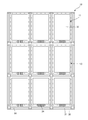
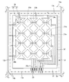
- FIG. 1 is a plan view showing a touch panel mother board according to an embodiment of the present invention.
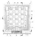
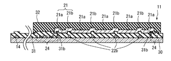
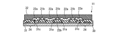
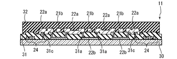
- FIG. 2 is an enlarged plan view around the touch panel unit 11 in FIG. 3 is a cross-sectional view taken along the line III-III in FIG. 4 is a cross-sectional view taken along the line IV-IV in FIG.
- FIG. 5 is an enlarged VV sectional view of FIG.
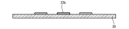
- FIG. 6A is a cross-sectional view showing a state where a bridge portion is formed on a substrate.
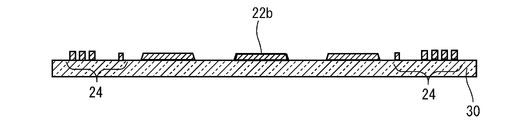
- FIG. 6B is a cross-sectional view showing a state in which the lead wiring is formed on the substrate.
- FIG. 6C is a cross-sectional view showing a state in which an insulating film is formed on the substrate.
- FIG. 6D is a cross-sectional view showing a state in which an electrode film is formed on the insulating film.
- FIG. 6E is a cross-sectional view showing a state in which a protective film is formed.
- FIG. 7 is an enlarged plan view of the periphery of the touch panel unit according to the second embodiment of the present invention.
- FIG. 8A is an enlarged plan view of the periphery of the touch panel unit according to the third embodiment of the present invention.
- FIG. 8B is an enlarged plan view of the discontinuous portion in FIG. 8A.
- FIG. 9 is an enlarged plan view of the periphery of the touch panel unit according to the fourth embodiment of the present invention.
- a touch panel mother board is a touch panel mother board in which a plurality of touch panel parts that become touch panels after cutting are formed, a plurality of electrodes provided in each of the plurality of touch panel parts, and the touch panel A conductive pattern formed outside the electrode, and an extended portion that is provided at both ends of each of the plurality of electrodes in the extending direction of each electrode and electrically connects the electrode and the conductive pattern (touch panel) First configuration of mother board).
- the extension part is for conducting each of the plurality of electrodes and a conductive pattern formed outside the touch panel part in order to allow static electricity in the touch panel part to flow out of the touch panel part.
- the extending portion includes a configuration having a discontinuous portion having a constant separation distance therein.
- static electricity generated in the touch panel unit can be discharged to a conductive pattern formed outside the touch panel unit.
- the outflow to the conductive pattern becomes more effective.
- static electricity that has occurred outside the touch panel portion and then entered the touch panel portion through one path can be caused to flow out of the touch panel section again from the other path.
- electrostatic breakdown in the touch panel portion is reduced, and the product yield can be improved.
- the conductive pattern and the extending part may be electrically connected across one side of the touch panel part (second structure of the touch panel mother board).
- the conductive pattern and the extending part are electrically connected across a plurality of sides of the touch panel part (third of the touch panel mother board). Configuration).
- the touch panel mother board in the vicinity of an extending portion provided on one end portion of each electrode (for example, a connection terminal to an external drive circuit is formed thereon) There are no unnecessary lead wires or the like when used as a touch panel. As a result, such a problem that the degree of freedom of terminal design of the drive circuit is deprived by such wiring is solved. Further, according to this configuration, the length of the lead-out wiring can be shortened. Thereby, the noise by the electrostatic capacitance formed in the lead-out wiring part can be reduced.
- a touch panel mother board is the touch panel mother board according to any one of the first to third configurations having a discontinuous portion in at least a part of the extending portion (touch panel mother board). Fourth configuration of the substrate).
- the fourth configuration of the touch panel mother board by appropriately setting the separation distance of the discontinuous part, static electricity generated in the touch panel part can flow out of the touch panel part beyond the discontinuous part. .
- a discontinuous portion By providing such a discontinuous portion, it is possible to cope with a design when it is desirable not to connect each electrode and the conductive pattern outside the touch panel portion.
- the degree of freedom in design can be increased by using a conductive pattern as an inspection electrode in the manufacturing process.
- the touch panel portion further includes a plurality of lead wires that are led out from the electrodes, and a separation distance between the discontinuous portions is smaller than a minimum distance between the plurality of lead wires. It is desirable to do this (fifth configuration of the touch panel mother board).
- the distance between the discontinuous portions is made smaller than the minimum distance between the plurality of lead wires included in the touch panel portion, thereby preventing electrostatic breakdown in the touch panel portion. be able to.
- the distal ends of the discontinuous portions of the extending portions may have convex shapes facing each other (sixth structure of the touch panel mother board).
- a touch panel according to an embodiment of the present invention is a touch panel cut out from a touch panel motherboard according to any one of the first to sixth configurations.
- the manufacturing method of the touch panel which concerns on one Embodiment of this invention is a manufacturing method of a touch panel including the process of forming the touch-panel mother board
- the step of forming the touch panel mother substrate includes forming a plurality of electrodes of the touch panel on the translucent substrate, and forming a conductive pattern outside the touch panel portion on the translucent substrate; And a step of forming an extension portion for electrically connecting the electrode and the conductive pattern at both ends in the extending direction of each electrode in each of the plurality of electrodes.
- the touch panel mother board and the touch panel according to the present invention may include arbitrary constituent members that are not shown in the drawings referred to in this specification.
- the dimension of the member in each figure does not represent the dimension of an actual structural member, the dimension ratio of each member, etc. faithfully.
- FIG. 1 shows a touch panel mother board 10 according to an embodiment of the present invention.
- a plurality of touch panel portions 11 that become a touch panel after cutting are formed on the touch panel mother substrate 10.
- a conductive pattern 14 is formed around the entire touch panel substrate 10 around the touch panel portion 11.
- the conductive pattern 14 is electrically connected to each touch panel unit 11 via a lead-out wiring (extension portion) 24, and plays a role of discharging static electricity inside the touch panel unit 11 to the outside of the touch panel unit 11. Yes.
- the conductive pattern 14 and the lead wiring 24 are covered with an insulating film 31 as will be described later. In order to make the drawing easy to see, the conductive pattern 14 and the lead-out wiring 24 are shown by solid lines in FIG.
- Each touch panel unit 11 is cut and separated along the parting line 13 and then connected to an external drive circuit (not shown) to form a touch panel. By cutting, each touch panel unit 11 and the conductive pattern 14 are separated, and the short circuit state is released.
- FIG. 2 is an enlarged plan view of the touch panel unit 11 and its periphery.
- 3 is a sectional view taken along line III-III in FIG. 2
- FIG. 4 is a sectional view taken along line IV-IV in FIG. 2
- FIG. 5 is an enlarged sectional view taken along line VV in FIG.
- the touch panel according to this embodiment includes an electrode 20 on a substrate 30.
- a capacitance is formed between the electrode 20 and the finger close to the operation surface, so that the touch position is obtained from a difference in capacitance between the electrode and the finger depending on the touch position. It is configured. That is, the touch panel of the present embodiment is a so-called capacitance type touch panel.
- the electrode 20 has a plurality of first direction electrodes 21 extending in one direction and a plurality of second direction electrodes 22 extending in a direction intersecting with the first direction electrodes 21.
- the first direction electrode 21 is formed by integrally molding a plurality of island-shaped electrode portions 21a and connecting portions 21b that connect the island-shaped electrode portions 21a. Arbitrary numbers of the first direction electrodes are arranged so as to be substantially perpendicular to the extending direction.
- the second direction electrode 22 includes a plurality of island electrode portions 22a and a bridge portion 22b that connects the island electrode portions 22a. Arbitrary numbers of the second direction electrodes are arranged so as to be substantially perpendicular to the extending direction.
- the bridge portion 22b is formed on a layer different from the island-like electrode portions 21a and 22a and the connection portion 21b with the insulating film 31 interposed therebetween. That is, the bridge portion 22 b is disposed so as to pass under the connection portion 21 b of the first direction electrode 21. As shown in FIG. 4, the island-shaped electrode portion 22 a and the bridge portion 22 b are electrically connected through a contact hole 31 a formed in the insulating film 31.
- lead wires 24 are connected to both ends of each first direction electrode 21 and each second direction electrode 22 in the extending direction.
- a part of the lead wiring 24 includes a terminal portion 25 formed of a conductive film in the vicinity of the extended end.
- the lead wiring 24 extends to the outside of the touch panel unit 11 and is electrically connected to the conductive pattern 14.
- the lead-out wiring 24 is formed on a layer different from the island-shaped electrode portions 21a and 22a and the terminal portion 25 with the insulating film 31 interposed therebetween.
- the lead-out wiring 24 has an island-like electrode portion 21a through the contact hole 31b, an island-like electrode 22a through the contact hole 31c as shown in FIG. 4, and a terminal portion through the contact hole 31d as shown in FIG. 25, respectively.
- a conductive film is formed on an insulating substrate 30 such as glass by a CVD (Chemical Vapor Deposition) method, a sputtering method, or the like.
- Various materials can be used as the conductive film.
- ITO Indium Tin Oxide
- a resist pattern that covers a region where the bridge portion 22b is to be formed is formed by photolithography, and the conductive film is etched using the resist pattern as a mask. Thereby, as shown to FIG. 6A, the bridge
- a metal film such as an aluminum alloy is formed on the substrate 30, and a metal film such as titanium having a low reflectance is further formed on the metal film.
- a resist pattern is formed by photolithography to cover a region where the lead wiring 24 and the conductive pattern 14 (not shown) are to be formed, and the metal film is etched using the resist pattern as a mask. As a result, as shown in FIG. 6B, the lead-out wiring 24 and the conductive pattern 14 (not shown) are obtained. Thereafter, the formed resist pattern is removed.
- an insulating film 31 is formed so as to cover the substrate 30, the bridge portion 22b, the lead wiring 24, and the conductive pattern 14 (not shown).
- the insulating film 31 is made of, for example, a silicon oxide film or a silicon nitride film, and is formed by a CVD method, a sputtering method, or the like.
- a resist pattern covering a region other than a region where contact holes 31a to 31d (31b and 31d are not shown) are to be formed is formed by photolithography, and the insulating film is etched using the resist pattern as a mask. Thus, contact holes 31a to 31d (31b and 31d are not shown) are formed in the insulating film 31. Thereafter, the formed resist pattern is removed.
- a conductive film 33 is formed on the insulating film 31 by CVD, sputtering, or the like. At this time, since the conductive film 33 is also formed in the contact holes 31a to 31d (31b and 31d are not shown) formed in the insulating film 31, the conductive film 33, the bridge portion 22b, and the lead wiring 24 are formed. Electrically connected. Then, by photolithography, the island-like electrode portion 21a (not shown) of the first direction electrode 21, the connection portion 21b of the first direction electrode 21, the island-like electrode portion 22a of the second direction electrode 22, and the terminal portion 25 (not shown).
- a resist pattern that covers a region to be formed is formed, and the conductive film 33 is etched using the resist pattern as a mask. Thereby, the island-shaped electrode portion 21a (not shown) of the first direction electrode 21, the connection portion 21b of the first direction electrode 21, the island-shaped electrode portion 22a of the second direction electrode 22 and the terminal portion 25 (not shown) are formed. To do. Thereafter, the formed resist pattern is removed.
- a protective film 32 is formed on the insulating film 31 and the electrode 20.
- the protective film 32 is made of, for example, an acrylic or siloxane organic material film, and is formed by a spin coat coating method, a spray coating method, or the like. At this time, using a metal mask or the like, the protective film 32 is not formed near the dividing line 13 and the terminal portion 25 as shown in FIGS.
- Each touch panel unit 11 is cut and cut along a dividing line 13 shown in FIGS. 1 and 2, and then connected to an external drive circuit (not shown) to form a touch panel.
- an external drive circuit not shown
- each touch panel unit 11 and the conductive pattern 14 are separated, and the short circuit state is released.
- Various means such as a wheel cutter, a wire saw, and a laser can be used for cutting.
- the first direction electrode 21 is connected to the lead-out wiring 24 from both ends via the contact hole 31b
- the second direction electrode 22 is connected to the lead-out wiring 24 from both ends via the contact hole 31c.
- the lead wiring 24 is connected to the conductive pattern 14 formed outside the touch panel portion. Thereby, the static electricity inside the touch panel part 11 can be efficiently discharged to the conductive pattern 14.
- the above-mentioned embodiment is one illustration of this invention, Comprising:
- This invention is not limited.
- the shape of the electrode 20 is not limited to that according to the above-described embodiment, and can take various shapes.
- what was mentioned above also as a material of each structural member is only an illustration, and various materials can be used according to a use.
- the touch panel unit 11 is configured in a substantially rectangular shape, but may take various shapes such as a parallelogram and a polygon.
- the electroconductive pattern 14 illustrated the structure integrally formed over the whole touch-panel mother substrate 10, you may form in multiple numbers as needed.
- FIG. 7 shows an enlarged plan view of the touch panel portion 11a of the touch panel mother board according to the second embodiment and its periphery.
- the configuration of this embodiment is the same as that of the above-described first embodiment except for the lead-out wiring 24 and the conductive pattern 14. Therefore, in the following description, in the same part as the first embodiment, Only the different parts with the same reference numerals will be described.
- the first direction electrode 21 is electrically connected to the lead-out wiring 24a at one end and is electrically connected to the lead-out wiring 24b at the other end.
- the second direction electrode 22 is electrically connected to the lead-out wiring 24a at one end and is electrically connected to the lead-out wiring 24c at the other end.
- a conductive pattern 14a is formed around the touch panel portion 11a so as to surround the touch panel portion 11a.
- the lead-out wiring 24a extends to the outside of the touch panel portion 11a across the dividing line 13a, which is one side of the dividing line 13, and is electrically connected to the conductive pattern 14a.
- the lead-out wiring 24a is electrically connected to the terminal portion 25 in the vicinity of the dividing line 13a.
- the lead-out wiring 24b extends to the outside of the touch panel portion 11a across the dividing line 13b which is a side different from the dividing line 13a in the dividing line 13, and is electrically connected to the conductive pattern 14a.
- the lead-out wiring 24c extends to the outside of the touch panel portion 11a across the dividing line 13c, which is a side different from the dividing line 13a and the dividing line 13b, and is electrically connected to the conductive pattern 14a. Has been.
- the above-mentioned embodiment is one illustration of this invention, Comprising: This invention is not limited.
- the touch panel portion 11a has a substantially rectangular shape, and the lead wires 24a to 24c are extended from three mutually different sides.
- the lead lines 24a to 24c are extended from two different sides, or the lead lines 24a to 24c are extended from four different sides.
- the touch panel portion 11a is polygonal, and the lead wires 24a to 24c are extended from more sides.
- the conductive pattern 14a showed the structure surrounding the circumference
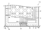
- FIG. 8A shows an enlarged plan view of the touch panel portion 11b of the touch panel mother board 10 according to the third embodiment and the periphery thereof. Since the configuration of this embodiment is the same as that of the above-described second embodiment except for the lead-out wiring 24a, the same reference numerals are given to the same portions as those of the second embodiment in the following description. Only different parts will be described.
- the lead wiring 24d electrically connected to one end of the electrode 20 has a discontinuous portion 40 between the conductive pattern 14a.
- FIG. 8B shows an enlarged plan view of the discontinuous portion 40.
- the lead-out wiring 24d has a separation portion 41 separated by a distance d. Since the distance d is short, static electricity can move through the separation portion 41. Specifically, the separation distance d is shorter than the minimum distance between adjacent strands such as the lead wires 24b and 24d in the touch panel portion 11b.
- the spacing portion tips 41a and 41b are formed in a substantially triangular shape facing each other.
- the discontinuous portion 40 is formed in the vicinity of the terminal portion 25, but this is merely an example.
- the position and number of the discontinuous portions 40 are not limited at all, and various configurations can be taken.
- the discontinuous portion 40 can be formed not in the lead wire 24d but in the lead wire 24b or the like, or the discontinuous portion 40 can be formed only in a part of the lead wire 24d.
- tips 41a and 41b illustrated the structure formed in the substantially triangular shape which mutually opposed, the separation-part front-end
- the spacing portion tips 41a and 41b can have various shapes such as convex shapes facing each other, for example, a trapezoidal shape or a semicircular shape.
- FIG. 9 shows an enlarged plan view of the touch panel portion 11c of the touch panel mother board 10 according to the fourth embodiment and the periphery thereof.
- the electrode 20 is connected to the lead-out wiring 24e at one end, and the other end of the electrode 20 is terminated inside the touch panel portion 11c.
- the present invention can be industrially used as a touch panel mother board capable of discharging static electricity generated in the touch panel section to the outside.
Landscapes
- Engineering & Computer Science (AREA)
- General Engineering & Computer Science (AREA)
- Theoretical Computer Science (AREA)
- Human Computer Interaction (AREA)
- Physics & Mathematics (AREA)
- General Physics & Mathematics (AREA)
- Computer Networks & Wireless Communication (AREA)
- Position Input By Displaying (AREA)
Abstract
タッチパネル内で発生した静電気又はタッチパネル外で発生した後にタッチパネル内へ侵入した静電気を、タッチパネル外へ効果的に流出させることができるタッチパネル母基板及びタッチパネルの構成を得る。切断後にタッチパネルとなるタッチパネル部(11)が複数形成されたタッチパネル母基板であって、前記複数のタッチパネル部(11)の各々に設けられた複数の電極(21,22)と、前記タッチパネル部(11)の外に形成された導電性パターン(14)と、前記複数の電極の各々において各電極の延在方向における両端部に設けられ、当該電極と前記導電性パターンとを導通させる延出部(24)とを備える。
Description
本発明は、タッチパネル母基板、該タッチパネル母基板から切り出されたタッチパネルおよびその製造方法に関する。
従来、操作面上でペンや指等がタッチした位置、すなわちタッチ位置を検出可能なタッチパネルが知られている。このようなタッチパネルは、例えば特開2010-160670号公報に開示されるように、基板上に、互いに交差する方向に延在する複数の第一電極及び第二電極を有している。
前記特開2010-160670号公報に開示されている構成では、タッチパネルをタッチする指と前記第一電極及び第二電極との間にそれぞれ静電容量が形成される。そして、これらの静電容量を検出することによって、操作面のタッチ位置を検出することができる。すなわち、前記特開2010-160670号公報に開示されている構成は、いわゆる静電容量型のタッチパネルである。
タッチパネルの製造過程において、大判基板(タッチパネル母基板)に複数のタッチパネルを配置してパターン形成した後、タッチパネル母基板からタッチパネルを切断分離する工程が存在する。この工程において、運搬や膜面保護処理等によって静電気が発生し易く、静電破壊によるパターン破壊が起こり製品歩留まりを低下させるという問題があった。
そのため、以下の開示においては、タッチパネル内で発生した静電気又はタッチパネル外で発生した後にタッチパネル内へ侵入した静電気を、タッチパネル外に効果的に流出させることができるタッチパネル母基板及びタッチパネルの構成を得ることを目的とする。
本発明の一実施形態に係るタッチパネル母基板は、切断後にタッチパネルとなるタッチパネル部が複数形成されたタッチパネル母基板であって、前記複数のタッチパネル部の各々に設けられた複数の電極と、前記タッチパネル部外に形成された導電性パターンと、前記複数の電極の各々において各電極の延在方向における両端部に設けられ、当該電極と前記導電性パターンとを導通させる延出部とを備える。
また、本発明の一実施形態に係るタッチパネルの製造方法は、複数のタッチパネルを有するタッチパネル母基板を形成する工程と、当該タッチパネル母基板から前記タッチパネルを分離する工程とを含み、前記タッチパネル母基板を形成する工程が、透光性基板上に、前記タッチパネルの複数の電極を形成する工程と、前記透光性基板上において前記タッチパネル部外に導電性パターンを形成する工程と、前記複数の電極の各々において各電極の延在方向における両端部に、当該電極と前記導電性パターンとを導通させる延出部を形成する工程とを含む。
なお、前記製造方法において、透光性基板上に、前記タッチパネルの複数の電極を形成する工程と、前記透光性基板上において前記タッチパネル部外に導電性パターンを形成する工程と、前記複数の電極の各々において各電極の延在方向における両端部に、当該電極と前記導電性パターンとを導通させる延出部を形成する工程とは、必ずしもこの順番に行われなくても良く、また、このうちの幾つか又はすべての工程を、同時に行っても良い。
本発明の一実施形態にかかるタッチパネル母基板によって、タッチパネル部内で発生した静電気又はタッチパネル部外で発生した後にタッチパネル部内へ侵入した静電気を、タッチパネル部外に効果的に流出させることができる。
本発明の一実施形態に係るタッチパネル母基板は、切断後にタッチパネルとなるタッチパネル部が複数形成されたタッチパネル母基板であって、前記複数のタッチパネル部の各々に設けられた複数の電極と、前記タッチパネル部外に形成された導電性パターンと、前記複数の電極の各々において各電極の延在方向における両端部に設けられ、当該電極と前記導電性パターンとを導通させる延出部とを備える(タッチパネル母基板の第一の構成)。
ここで前記延出部は、タッチパネル部内の静電気をタッチパネル部外へ流出させるために、前記複数の電極の各々とタッチパネル部外に形成された導電性パターンとを導通させるものであり、具体的には導電性膜により形成された配線や、前記電極を基板周縁まで延出させた構成等を例示できる。後述するように、前記延出部には、その中に一定の離間距離を有した不連続部を有する構成を含む。
タッチパネル母基板の第一の構成によれば、タッチパネル部内で発生した静電気を、タッチパネル部外に形成された導電性パターンへ流出させることができる。特に各電極の延在方向両端から導電性パターンへ導通させることにより、導電性パターンへの流出がより効果的になる。また、タッチパネル部外で発生した後に一の経路を通じてタッチパネル部内へ侵入した静電気を、他方の経路より再びタッチパネル部外へ流出させることができる。その結果、タッチパネル部内での静電破壊が減少し、製品歩留まりを向上させることができる。
前記タッチパネル母基板の第一の構成において、前記導電性パターンと前記延出部とが、前記タッチパネル部の一辺を横切って導通する構成とすることができる(タッチパネル母基板の第二の構成)。
また、前記タッチパネル母基板の第一の構成において、前記導電性パターンと前記延出部とが、前記タッチパネル部の複数の辺を横切って導通する構成とすることが望ましい(タッチパネル母基板の第三の構成)。
タッチパネル母基板の第三の構成によれば、各電極の一方の端部に設けられた延出部(この上には例えば、外部駆動回路への接続端子が形成されている)の近傍に、タッチパネルとして使用する際に不要な引き出し配線等が存在しない。この結果、このような配線により駆動回路の端子設計の自由度が奪われるという問題が解消される。また、この構成によれば引き出し配線の長さを短くすることができる。これにより、引き出し配線部分に形成される静電容量によるノイズを低減できる。
本発明の他の実施形態に係るタッチパネル母基板は、前記延出部の少なくとも一部に不連続部を有する、前記第一~第三の構成のいずれかに係るタッチパネル母基板である(タッチパネル母基板の第四の構成)。
タッチパネル母基板の第四の構成によれば、不連続部の離間距離が適切に設定されることにより、タッチパネル部内で発生した静電気を、不連続部を超えてタッチパネル部外へ流出させることができる。このような不連続部を設けることにより、各電極とタッチパネル部外の導電性パターンとを接続しない方が望ましい場合の設計対応が可能になる。例えば、導電性パターンを製造過程における検査用電極として使用する等、設計の自由度を高めることができる。
前記タッチパネル母基板の第四の構成において、前記タッチパネル部が、前記電極から引き出される複数の引き出し配線をさらに備え、前記不連続部の離間距離が、前記複数の引き出し配線間の最小距離よりも小さくすることが望ましい(タッチパネル母基板の第五の構成)。
タッチパネル母基板の第五の構成によれば、前記不連続部の離間距離が、前記タッチパネル部が備える複数の引き出し配線間の最小距離よりも小さくすることによって、タッチパネル部内での静電破壊を防ぐことができる。
前記タッチパネル母基板の第四または第五の構成において、前記延出部の不連続部の先端が、互いに対向する凸形状とすることができる(タッチパネル母基板の第六の構成)。
本発明の一実施形態に係るタッチパネルは、前記第一~第六の構成のいずれかに係るタッチパネル母基板から切り出されたタッチパネルである。
本発明の一実施形態に係るタッチパネルの製造方法は、複数のタッチパネルを有するタッチパネル母基板を形成する工程と、当該タッチパネル母基板から前記タッチパネルを分離する工程とを含む、タッチパネルの製造方法であって、前記タッチパネル母基板を形成する工程が、透光性基板上に、前記タッチパネルの複数の電極を形成する工程と、前記透光性基板上において前記タッチパネル部外に導電性パターンを形成する工程と、前記複数の電極の各々において各電極の延在方向における両端部に、当該電極と前記導電性パターンとを導通させる延出部を形成する工程とを含む。
以下、本発明のより具体的な実施形態について図面を参照しながら説明する。なお、以下で参照する各図は、説明の便宜上、本発明の実施形態の構成部材のうち、本発明を説明するために必要な主要部材のみを簡略化して示したものである。従って、本発明に係るタッチパネル母基板及びタッチパネルは、本明細書が参照する各図に示されていない任意の構成部材を備え得る。また、各図中の部材の寸法は、実際の構成部材の寸法及び各部材の寸法比率等を忠実に表したものではない。
(第一の実施形態)
図1には、本発明の一実施形態に係るタッチパネル母基板10が示されている。タッチパネル母基板10上には、切断後にタッチパネルとなるタッチパネル部11が複数形成されている。タッチパネル部11の周辺には、タッチパネル母基板10の全体にわたって導電性パターン14が形成されている。導電性パターン14は、各タッチパネル部11と引き出し配線(延出部)24を介して電気的に接続されており、タッチパネル部11の内部の静電気をタッチパネル部11の外部へ流出させる役割を担っている。
図1には、本発明の一実施形態に係るタッチパネル母基板10が示されている。タッチパネル母基板10上には、切断後にタッチパネルとなるタッチパネル部11が複数形成されている。タッチパネル部11の周辺には、タッチパネル母基板10の全体にわたって導電性パターン14が形成されている。導電性パターン14は、各タッチパネル部11と引き出し配線(延出部)24を介して電気的に接続されており、タッチパネル部11の内部の静電気をタッチパネル部11の外部へ流出させる役割を担っている。
なお、導電性パターン14及び引き出し配線24は、後述するように、絶縁膜31により覆われている。図を見易くするため、図1では、導電性パターン14及び引き出し配線24を実線で示している。
各タッチパネル部11は分断線13に沿って切断され切り離された後、図示しない外部駆動回路と接続されてタッチパネルとなる。切断により各タッチパネル部11と導電性パターン14とが切り離され、短絡状態が解除される。
図2~図5を用いて、タッチパネル部11の詳細について説明する。図2は、タッチパネル部11及びその周辺の拡大平面図である。図3は図2におけるIII-III断面図、図4は図2におけるIV-IV断面図、図5は図2におけるV-V拡大断面図である。
図2に示すように、本実施形態に係るタッチパネルは、基板30上に、電極20を備えている。本タッチパネルは、電極20と操作面に近づけた手指との間に静電容量が形成されることにより、タッチ位置による各電極と手指との間の静電容量の差から該タッチ位置を求めるように構成されている。すなわち、本実施形態のタッチパネルは、いわゆる静電容量型のタッチパネルである。
電極20は、一方向に延在した複数の第一方向電極21と、これと交差する方向に延在した複数の第二方向電極22とを有する。第一方向電極21は、複数の島状電極部21aと、該島状電極部21a同士を接続する接続部21bとが一体成型されたものである。第一方向電極は延在方向と略垂直に整列して、任意の数が配置される。第二方向電極22は、複数の島状電極部22aと、該島状電極部22a同士を接続するブリッジ部22bとを有する。第二方向電極は延在方向と略垂直に整列して、任意の数が配置される。
前記ブリッジ部22bは、図3および図4に示すように、絶縁膜31を挟んで島状電極部21a,22a及び接続部21bとは異なる層上に形成されている。すなわち、ブリッジ部22bは第一方向電極21の接続部21bの下をくぐるように配置されている。図4に示すように、島状電極部22aとブリッジ部22bは、絶縁膜31に形成されたコンタクトホール31aを通じて電気的に接続されている。
図2に示すように、各第一方向電極21及び各第二方向電極22の延在方向両端部には、引き出し配線24が接続されている。引き出し配線24の一部は、その延出端近傍に導電性膜により形成された端子部25を備える。引き出し配線24はタッチパネル部11の外側まで延出しており、導電性パターン14と電気的に接続している。
なお、導電性パターン及び引き出し配線24は絶縁膜31で覆われている。図を見易くするため、図2においては保護膜32で覆われた部分のみ破線で示し、他は実線で示した。図7~図9においても同様である。
図3~図5に示すように引き出し配線24は、絶縁膜31を挟んで島状電極部21a,22a,及び端子部25とは異なる層上に形成されている。引き出し配線24は、図3に示すようにコンタクトホール31bを通じて島状電極部21aと、図4に示すようにコンタクトホール31cを通じて島状電極22aと、図5に示すようにコンタクトホール31dを通じて端子部25と、それぞれ電気的に接続されている。
(第一の実施形態に係るタッチパネル母基板及びタッチパネルの製造方法)
続いて、上述のタッチパネル母基板10及び該タッチパネル母基板10から切り出されるタッチパネルの製造方法について、図6A~図6Eを用いて説明する。
続いて、上述のタッチパネル母基板10及び該タッチパネル母基板10から切り出されるタッチパネルの製造方法について、図6A~図6Eを用いて説明する。
まず、ガラス等の絶縁性基板30上に、CVD(Chemical Vapor Deposition)法やスパッタ法等によって導電性膜を形成する。導電性膜としては、種々の材料を用いることができるが、例えば透明導電性材料としてITO(Indium Tin Oxide)等が用いられる。そして、フォトリソグラフィ法により、ブリッジ部22bを形成する予定の領域を覆うレジストパターンを形成し、これをマスクとして前記導電性膜をエッチングする。これにより、図6Aに示すように、ブリッジ部22bが得られる。その後、形成したレジストパターンを除去する。
次に、基板30上にアルミニウム合金等の金属膜を形成し、この金属膜上にさらに、反射率の低いチタン等の金属膜を形成する。そして、フォトリソグラフィ法により、引き出し配線24及び導電性パターン14(図示しない)を形成する予定の領域を覆うレジストパターンを形成し、これをマスクとして前記金属膜をエッチングする。これにより、図6Bに示すように、引き出し配線24及び導電性パターン14(図示しない)が得られる。その後、形成したレジストパターンを除去する。
次に、図6Cに示すように、基板30、ブリッジ部22b、引き出し配線24及び導電性パターン14(図示しない)を覆うように絶縁膜31を形成する。この絶縁膜31は、例えば酸化シリコン膜や窒化シリコン膜等からなり、CVD法やスパッタ法等により形成される。そして、フォトリソグラフィ法により、コンタクトホール31a~31d(31b及び31dは図示しない)を形成する予定の領域以外を覆うレジストパターンを形成し、これをマスクとして前記絶縁膜をエッチングする。これにより、絶縁膜31にコンタクトホール31a~31d(31b及び31dは図示しない)を形成する。その後、形成したレジストパターンを除去する。
次に、図6Dに示すように、絶縁膜31上に、CVD法やスパッタ法等によって、導電性膜33を形成する。このとき、絶縁膜31に形成されたコンタクトホール31a~31d(31b及び31dは図示しない)内にも導電性膜33が形成されるため、導電性膜33とブリッジ部22b及び引き出し配線24とが電気的に接続される。そして、フォトリソグラフィ法によって、第一方向電極21の島状電極部21a(図示しない)、第一方向電極21の接続部21b、第二方向電極22の島状電極部22a及び端子部25(図示しない)を形成する予定の領域を覆うレジストパターンを形成し、これをマスクとして、導電性膜33をエッチングする。これにより、第一方向電極21の島状電極部21a(図示しない)、第一方向電極21の接続部21b、第二方向電極22の島状電極部22a及び端子部25(図示しない)を形成する。その後、形成したレジストパターンを除去する。
次に、図6Eに示すように、絶縁膜31、電極20上に保護膜32を形成する。保護膜32は、例えばアクリル系又はシロキサン系の有機材料膜等が用いられ、スピンコート塗布法やスプレー塗布法等によって形成される。この際、メタルマスク等を用いて、図1及び図2に示すように分断線13及び端子部25の近傍には保護膜32を形成しないようにする。
各タッチパネル部11は図1及び図2に示す分断線13に沿って切断され切り離された後、図示しない外部駆動回路と接続されてタッチパネルとなる。切断により各タッチパネル部11と導電性パターン14とが切り離され、短絡状態が解除される。切断にはホイールカッター、ワイヤーソー、レーザー等の種々の手段を用いることができる。
(第一の実施形態の効果)
以上より、この実施形態では、第一方向電極21はその両端からコンタクトホール31bを介して引き出し配線24に接続されており、第二方向電極22はその両端からコンタクトホール31cを介して引き出し配線24に接続している。さらに、引き出し配線24はタッチパネル部外部に形成された導電性パターン14に接続されている。これにより、タッチパネル部11の内部の静電気を効率的に導電性パターン14へ流出させることができる。
以上より、この実施形態では、第一方向電極21はその両端からコンタクトホール31bを介して引き出し配線24に接続されており、第二方向電極22はその両端からコンタクトホール31cを介して引き出し配線24に接続している。さらに、引き出し配線24はタッチパネル部外部に形成された導電性パターン14に接続されている。これにより、タッチパネル部11の内部の静電気を効率的に導電性パターン14へ流出させることができる。
なお、上述の実施形態は本発明の一つの例示であって、本発明を限定するものではない。例えば、電極20の形状は上述の実施形態に係るものに限定されず、種々の形状を取り得る。また、各構成部材の材料も上述したものは例示に過ぎず、用途に応じて種々の材料を用い得る。本実施形態ではタッチパネル部11は略長方形に構成されているが、平行四辺形や、多角形等の種々の形状を取り得る。導電性パターン14は、タッチパネル母基板10全体にわたって一体に形成する構成を例示したが、必要に応じて複数形成してもよい。
(第二の実施形態)
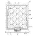
図7に、第二の実施形態に係るタッチパネル母基板のタッチパネル部11a及びその周辺の拡大平面図を示す。この実施形態の構成は、引き出し配線24及び導電性パターン14等を除くほか、上述の第一の実施形態と同じ構成であるため、以下の説明において、第一の実施形態と同一の部分には同一の符号を付して異なる部分についてのみ説明する。
図7に、第二の実施形態に係るタッチパネル母基板のタッチパネル部11a及びその周辺の拡大平面図を示す。この実施形態の構成は、引き出し配線24及び導電性パターン14等を除くほか、上述の第一の実施形態と同じ構成であるため、以下の説明において、第一の実施形態と同一の部分には同一の符号を付して異なる部分についてのみ説明する。
図7に示すように、第一方向電極21は、一方の端部において引き出し配線24aと電気的に接続されており、もう一方の端部において引き出し配線24bと電気的に接続されている。また、第二方向電極22は、一方の端部において引き出し配線24aと電気的に接続されており、もう一方の端部において引き出し配線24cと電気的に接続されている。タッチパネル部11aの周囲には、タッチパネル部11aを囲むように導電性パターン14aが形成されている。
引き出し配線24aは、分断線13の一辺である分断線13aを横切って、タッチパネル部11aの外部に延出しており、導電性パターン14aと電気的に接続されている。また、引き出し配線24aは、分断線13aの近傍で端子部25と電気的に接続されている。
引き出し配線24bは、分断線13のうち、分断断線13aとは異なる辺である分断線13bを横切ってタッチパネル部11aの外部に延出しており、導電性パターン14aと電気的に接続されている。
引き出し配線24cは、分断線13のうち、分断線13a及び分断線13bとは異なる辺である分断線13cを横切ってタッチパネル部11aの外部に延出しており、導電性パターン14aと電気的に接続されている。
(第二の実施形態の効果)
この実施形態では、駆動回路に接続される端子部25の近傍に、タッチパネルとして使用する際は不要となる引き出し配線24b及び24cが存在しない。この結果、このような引き出し配線24b及び24cにより駆動回路の端子設計の自由度が奪われるという問題が解消される。また、この構成によれば引き出し配線24b及び24cの長さを短くすることができる。これにより、引き出し配線24b及び24cに形成される静電容量によるノイズを低減できる。
この実施形態では、駆動回路に接続される端子部25の近傍に、タッチパネルとして使用する際は不要となる引き出し配線24b及び24cが存在しない。この結果、このような引き出し配線24b及び24cにより駆動回路の端子設計の自由度が奪われるという問題が解消される。また、この構成によれば引き出し配線24b及び24cの長さを短くすることができる。これにより、引き出し配線24b及び24cに形成される静電容量によるノイズを低減できる。
なお、上述の実施形態は本発明の一つの例示であって、本発明を限定するものではない。本実施形態ではタッチパネル部11aの形状を略長方形としており、その相互に異なる3つの辺から引き出し配線24a~24cを延出させている。しかし例えば、相互に異なる2つの辺から引き出し配線24a~24cを延出させたり、相互に異なる4つの辺から引き出し配線24a~24cを延出させたりする構成も取り得る。さらにタッチパネル部11aを多角形とし、より多くの辺から引き出し配線24a~24cを延出させる構成も取り得る。また、導電性パターン14aがタッチパネル部11aの周囲を囲む構成を示したが、このような構成は本発明の必須の構成要件ではなく、導電性パターン14aは必要に応じて種々の形状に形成し得る。
(第三の実施形態)
図8Aに、第三の実施形態に係るタッチパネル母基板10のタッチパネル部11b及びその周辺の拡大平面図を示す。この実施形態の構成は、引き出し配線24aを除くほか、上述の第二の実施形態と同じ構成であるため、以下の説明において、第二の実施形態と同一の部分には同一の符号を付して異なる部分についてのみ説明する。
図8Aに、第三の実施形態に係るタッチパネル母基板10のタッチパネル部11b及びその周辺の拡大平面図を示す。この実施形態の構成は、引き出し配線24aを除くほか、上述の第二の実施形態と同じ構成であるため、以下の説明において、第二の実施形態と同一の部分には同一の符号を付して異なる部分についてのみ説明する。
図8Aに示すように、電極20の一方の端部と電気的に接続している引き出し配線24dは導電性パターン14aとの間に、不連続部40を有する。図8Bに不連続部40の拡大平面図を示す。詳しくは図8Bに示すように、引き出し配線24dは距離dを隔てて分離した離間部41を有する。距離dが短いため、静電気はこの離間部41を通じて移動することができる。離間距離dは、具体的にはタッチパネル部11b内の引き出し配線24bや24d等の隣接する素線間の最小距離より短く形成される。離間部先端41a及び41bは、互いに対向した略三角形状に形成されている。
(第三の実施形態の効果)
この実施形態では、離間部41の離間距離dが小さいため、タッチパネル部11bの内部で発生した静電気を、不連続部40を超えてタッチパネル部11bの外部へ流出させることができる。このとき、離間距離dを該タッチパネル部11b内の引き出し配線24bや24d等の隣接する素線間の最小距離より小さくすることによって、タッチパネル部11bの内部での静電破壊を防いでいる。この様な不連続部40を有することにより、各電極20とタッチパネル部11bの外部の導電性パターン14aとを接続しない方が望ましい場合の設計対応が可能になる。例えば、導電性パターン14aを製造過程における検査用電極として使用する等、設計の自由度を高めることができる。
この実施形態では、離間部41の離間距離dが小さいため、タッチパネル部11bの内部で発生した静電気を、不連続部40を超えてタッチパネル部11bの外部へ流出させることができる。このとき、離間距離dを該タッチパネル部11b内の引き出し配線24bや24d等の隣接する素線間の最小距離より小さくすることによって、タッチパネル部11bの内部での静電破壊を防いでいる。この様な不連続部40を有することにより、各電極20とタッチパネル部11bの外部の導電性パターン14aとを接続しない方が望ましい場合の設計対応が可能になる。例えば、導電性パターン14aを製造過程における検査用電極として使用する等、設計の自由度を高めることができる。
本実施形態において、不連続部40を端子部25の近傍に形成したが、これはあくまで例示である。不連続部40を形成する位置、数等は何ら限定されず、種々の構成を取り得る。例えば引き出し配線24dではなく、引き出し配線24b等に不連続部40を形成することもできるし、引き出し配線24dの一部のみに不連続部40を形成することもできる。また、離間部先端41a及び41bが互いに対向した略三角形状に形成された構成を例示したが、離間部先端41a及び41bは特に限定されない。離間部先端41a及び41bは、互いに対向する凸形状、例えば、台形形状や半円形形状といった種々の形状を取り得る。
(第四の実施形態)
図9に、第四の実施形態に係るタッチパネル母基板10のタッチパネル部11c及びその周辺の拡大平面図を示す。この実施形態では、電極20は一方の端部において引き出し配線24eと接続しており、電極20のもう一方の端部はタッチパネル部11cの内部で終端している。
図9に、第四の実施形態に係るタッチパネル母基板10のタッチパネル部11c及びその周辺の拡大平面図を示す。この実施形態では、電極20は一方の端部において引き出し配線24eと接続しており、電極20のもう一方の端部はタッチパネル部11cの内部で終端している。
この構成によっても、タッチパネル部11cの内部で発生した静電気を、引き出し配線24eを介して、導電性パターン14へ流出させることが可能である。ただし、この構成では、タッチパネル部11cの外部で発生し、引き出し配線24eを介してタッチパネル部11cの内部に侵入した静電気の流出経路が存在しない。静電気を効果的に流出させるためには、第一の実施形態実施形態~第三の実施形態に係るタッチパネル母基板10の構成の方が有利である。
本発明は、タッチパネル部で発生した静電気を外部へ流出させることが可能なタッチパネル母基板として、産業上の利用が可能である。
Claims (8)
- 切断後にタッチパネルとなるタッチパネル部が複数形成されたタッチパネル母基板であって、
前記複数のタッチパネル部の各々に設けられた複数の電極と、
前記タッチパネル部外に形成された導電性パターンと、
前記複数の電極の各々において各電極の延在方向における両端部に設けられ、当該電極と前記導電性パターンとを導通させる延出部とを備えた、タッチパネル母基板。 - 前記導電性パターンと前記延出部とが、前記タッチパネルの一辺を横切って導通する、請求項1に記載のタッチパネル母基板。
- 前記導電性パターンと前記延部とが、前記タッチパネルの複数の辺を横切って導通する、請求項1に記載のタッチパネル母基板。
- 前記延出部の少なくとも一部に不連続部を有する、請求項1~3のいずれか一項に記載のタッチパネル母基板。
- 前記タッチパネル部が、前記電極から引き出される複数の引き出し配線をさらに備え、
前記不連続部の離間距離が、前記複数の引き出し配線間の最小距離よりも小さい、請求項4に記載のタッチパネル母基板。 - 前記延出部の離間部の先端が、互いに対向する凸形状である、請求項4または5に記載のタッチパネル母基板。
- 請求項1~6のいずれか一項に記載のタッチパネル母基板から分離されたタッチパネル。
- 複数のタッチパネルを有するタッチパネル母基板を形成する工程と、当該タッチパネル母基板から前記タッチパネルを分離する工程とを含む、タッチパネルの製造方法であって、
前記タッチパネル母基板を形成する工程が、
透光性基板上に、前記タッチパネルの複数の電極を形成する工程と、
前記透光性基板上において前記タッチパネル部外に導電性パターンを形成する工程と、
前記複数の電極の各々において各電極の延在方向における両端部に、当該電極と前記導電性パターンとを導通させる延出部を形成する工程とを含む、タッチパネルの製造方法。
Applications Claiming Priority (2)
| Application Number | Priority Date | Filing Date | Title |
|---|---|---|---|
| JP2011035590 | 2011-02-22 | ||
| JP2011-035590 | 2011-02-22 |
Publications (1)
| Publication Number | Publication Date |
|---|---|
| WO2012114958A1 true WO2012114958A1 (ja) | 2012-08-30 |
Family
ID=46720740
Family Applications (1)
| Application Number | Title | Priority Date | Filing Date |
|---|---|---|---|
| PCT/JP2012/053553 Ceased WO2012114958A1 (ja) | 2011-02-22 | 2012-02-15 | タッチパネル母基板、該タッチパネル母基板から切り出されたタッチパネルおよびその製造方法 |
Country Status (1)
| Country | Link |
|---|---|
| WO (1) | WO2012114958A1 (ja) |
Cited By (2)
| Publication number | Priority date | Publication date | Assignee | Title |
|---|---|---|---|---|
| JP2016053787A (ja) * | 2014-09-03 | 2016-04-14 | 凸版印刷株式会社 | タッチセンサー用基板 |
| US9760229B2 (en) | 2014-08-11 | 2017-09-12 | Mitsubishi Electric Corporation | Touch screen, touch panel, display, and electronic equipment |
Citations (2)
| Publication number | Priority date | Publication date | Assignee | Title |
|---|---|---|---|---|
| JPH04221926A (ja) * | 1990-12-25 | 1992-08-12 | Sharp Corp | 液晶表示装置の製造方法 |
| JPH0541568A (ja) * | 1991-08-02 | 1993-02-19 | Canon Inc | プリント基板のパターン配置方法 |
-
2012
- 2012-02-15 WO PCT/JP2012/053553 patent/WO2012114958A1/ja not_active Ceased
Patent Citations (2)
| Publication number | Priority date | Publication date | Assignee | Title |
|---|---|---|---|---|
| JPH04221926A (ja) * | 1990-12-25 | 1992-08-12 | Sharp Corp | 液晶表示装置の製造方法 |
| JPH0541568A (ja) * | 1991-08-02 | 1993-02-19 | Canon Inc | プリント基板のパターン配置方法 |
Cited By (2)
| Publication number | Priority date | Publication date | Assignee | Title |
|---|---|---|---|---|
| US9760229B2 (en) | 2014-08-11 | 2017-09-12 | Mitsubishi Electric Corporation | Touch screen, touch panel, display, and electronic equipment |
| JP2016053787A (ja) * | 2014-09-03 | 2016-04-14 | 凸版印刷株式会社 | タッチセンサー用基板 |
Similar Documents
| Publication | Publication Date | Title |
|---|---|---|
| TWI467449B (zh) | 電容式觸控板及其製造方法 | |
| US9229554B2 (en) | Touch screen panel for display device | |
| JP5220146B2 (ja) | タッチパネルのセンシング装置 | |
| TWI585623B (zh) | 觸控面板、觸控電極結構及其製作方法 | |
| JP6029842B2 (ja) | 静電容量式入力装置 | |
| US20150060125A1 (en) | Touch panel | |
| KR101669538B1 (ko) | 터치스크린패널 및 그 제조방법 | |
| US10042487B2 (en) | Touch panels and methods of manufacturing touch panels | |
| JP5588466B2 (ja) | タッチパネルの配線構造 | |
| JP5838131B2 (ja) | タッチオンレンズデバイスを製造するための方法 | |
| TWI489343B (zh) | Input device | |
| TWI438662B (zh) | 觸控面板及具有此觸控面板的觸控顯示面板 | |
| JP5520162B2 (ja) | 入力装置及びその製造方法 | |
| KR20150043798A (ko) | 터치 패널 및 터치 패널의 제조 방법 | |
| KR20160043585A (ko) | 터치 스크린 패널 | |
| US20150060253A1 (en) | Decorative substrate and touch panel | |
| EP2690534B1 (en) | Touch screen panel and fabrication method thereof | |
| US10331261B2 (en) | Touch panel | |
| KR101985894B1 (ko) | 터치 스크린 패널 및 그의 제조방법 | |
| KR20170014039A (ko) | 플렉서블 터치 패널 및 플렉서블 터치 패널의 제조 방법 | |
| KR20150104677A (ko) | 터치스크린 패널 | |
| WO2012114958A1 (ja) | タッチパネル母基板、該タッチパネル母基板から切り出されたタッチパネルおよびその製造方法 | |
| KR20150052682A (ko) | 터치 패널 및 이의 제조 방법 | |
| KR20140112892A (ko) | 터치 스크린 패널 및 그 제조 방법 | |
| KR20160123449A (ko) | 터치 스크린 패널 및 이의 제조방법 |
Legal Events
| Date | Code | Title | Description |
|---|---|---|---|
| 121 | Ep: the epo has been informed by wipo that ep was designated in this application |
Ref document number: 12750175 Country of ref document: EP Kind code of ref document: A1 |
|
| NENP | Non-entry into the national phase |
Ref country code: DE |
|
| 122 | Ep: pct application non-entry in european phase |
Ref document number: 12750175 Country of ref document: EP Kind code of ref document: A1 |
|
| NENP | Non-entry into the national phase |
Ref country code: JP |