WO2012114685A1 - 有機el表示装置の製造方法およびその方法により製造された有機el表示装置 - Google Patents
有機el表示装置の製造方法およびその方法により製造された有機el表示装置 Download PDFInfo
- Publication number
- WO2012114685A1 WO2012114685A1 PCT/JP2012/001029 JP2012001029W WO2012114685A1 WO 2012114685 A1 WO2012114685 A1 WO 2012114685A1 JP 2012001029 W JP2012001029 W JP 2012001029W WO 2012114685 A1 WO2012114685 A1 WO 2012114685A1
- Authority
- WO
- WIPO (PCT)
- Prior art keywords
- substrate
- organic
- resin
- display device
- sealing
- Prior art date
- Legal status (The legal status is an assumption and is not a legal conclusion. Google has not performed a legal analysis and makes no representation as to the accuracy of the status listed.)
- Ceased
Links
Images








Classifications
-
- H—ELECTRICITY
- H10—SEMICONDUCTOR DEVICES; ELECTRIC SOLID-STATE DEVICES NOT OTHERWISE PROVIDED FOR
- H10K—ORGANIC ELECTRIC SOLID-STATE DEVICES
- H10K59/00—Integrated devices, or assemblies of multiple devices, comprising at least one organic light-emitting element covered by group H10K50/00
- H10K59/80—Constructional details
- H10K59/87—Passivation; Containers; Encapsulations
- H10K59/871—Self-supporting sealing arrangements
- H10K59/8722—Peripheral sealing arrangements, e.g. adhesives, sealants
-
- H—ELECTRICITY
- H10—SEMICONDUCTOR DEVICES; ELECTRIC SOLID-STATE DEVICES NOT OTHERWISE PROVIDED FOR
- H10K—ORGANIC ELECTRIC SOLID-STATE DEVICES
- H10K59/00—Integrated devices, or assemblies of multiple devices, comprising at least one organic light-emitting element covered by group H10K50/00
- H10K59/80—Constructional details
- H10K59/87—Passivation; Containers; Encapsulations
- H10K59/871—Self-supporting sealing arrangements
- H10K59/8723—Vertical spacers, e.g. arranged between the sealing arrangement and the OLED
Definitions
- organic EL display devices have attracted attention as next-generation flat panel display devices.
- This organic EL display device is a self-luminous display device, has excellent viewing angle characteristics, high visibility, low power consumption, and can be reduced in thickness, so that demand is increasing.
- the organic EL display device includes a plurality of organic EL elements arranged in a predetermined arrangement, and each of the plurality of organic EL elements includes a first electrode (anode) formed on an insulating substrate, a first electrode An organic layer having a light emitting layer formed on one electrode and a second electrode (cathode) formed on the organic layer are provided.
- the organic layer is sensitive to moisture, it is necessary to block moisture from the outside air. Therefore, conventionally, the organic layer is sealed from moisture by sealing the organic layer between the first substrate on which the organic layer is formed and the second substrate provided to face the first substrate.
- a method has been proposed. More specifically, an organic EL display device including a resin adhesive that bonds a first substrate and a second substrate so as to seal an organic layer has been proposed.
- an organic EL display device using a sealing material made of frit glass (low melting glass) instead of a resin adhesive has been proposed. More specifically, for example, an organic EL display provided with a sealing material provided between the element substrate and the sealing substrate and welded between the element substrate and the sealing substrate so as to seal the organic EL element.
- An apparatus is disclosed. And by sealing the organic layer using such a sealing material made of frit glass, it becomes possible to block moisture and oxygen in the outside air compared to the case of using a resin adhesive. The sealing performance by the sealing material is improved (for example, see Patent Document 1).
- the frit glass forming the sealing material is heated and melted by irradiating the sealing material with a laser, thereby performing welding between the element substrate and the sealing substrate.
- a sealing material made of frit glass is provided between the element substrate and the sealing substrate. Therefore, when performing welding by laser irradiation, the element substrate and the sealing substrate move and shift occurs, resulting in a problem that the yield of the organic EL display device is lowered.
- the organic EL display device described in Patent Document 1 has a problem that the organic EL element is damaged by heat propagation caused by laser heating when welding is performed by laser irradiation.
- the present invention has been made in view of the above-described problems, and prevents the occurrence of misalignment between the element substrate and the sealing substrate during welding by laser irradiation, and damages to the organic EL element due to laser heating. It is an object of the present invention to provide an organic EL display device manufacturing method that can be reduced and an organic EL display device manufactured by the method.
- an organic EL display device manufacturing method of the present invention includes an organic EL element forming step for forming an organic EL element on a first substrate, and a resin material for forming a resin material on a second substrate.
- An application process, a paste material heating process in which an organic solvent is vaporized by heating and baking the paste material to form a seal material made of frit glass, an outer peripheral surface of the first substrate, and a second material of the seal material Substrate Periphery only the portion in contact with the heating by laser irradiation and, wherein at least and
- a paste material in which frit glass is added to an organic solvent is applied between the first substrate and the second substrate on the outer peripheral surface of the first substrate and the outer peripheral surface of the second substrate. It is applied so as to straddle, and the paste material is heated and baked to vaporize the organic solvent and form a sealing material made of frit glass.
- the second substrate is fixed. Therefore, the movement of the first substrate and the second substrate can be prevented when performing welding by laser irradiation. As a result, it is possible to prevent the occurrence of misalignment between the first substrate and the second substrate at the time of welding by laser irradiation, and to prevent the yield of the organic EL display device from being lowered.
- the spot diameter of the laser beam may be 0.1 mm or more and 1 mm or less in the welding step.
- moisture and oxygen in the outside air can be blocked by the sealing material without reducing the effect of reducing damage to the organic EL element due to heat propagation caused by laser heating.
- the organic EL display device manufacturing method of the present invention further includes a resin frame forming step of forming a resin frame on the second substrate before the resin material forming step, and in the resin material forming step, inside the resin frame, By dropping and injecting the resin material, the resin material is formed on the second substrate, and in the bonding body forming step, the resin material is uniformly diffused inside the resin frame in a vacuum atmosphere. Then, the first substrate and the second substrate may be bonded together.
- the resin frame functions as a pressure partition for maintaining a vacuum state inside the bonded substrate board by the first substrate and the second substrate
- the resin member can be formed by a dropping injection method. become.
- an increase in cost can be suppressed.
- a spacer for regulating the thickness of the resin member may be mixed in the resin frame.
- the thickness of the resin member can be regulated with high accuracy.
- the resin frame may be formed of an acrylic resin or an epoxy resin.
- a film-like resin material may be formed in the resin material forming step.
- the heating temperature when baking the paste material may be set to 200 ° C. or more and 500 ° C. or less in the paste material heating step.
- the same effect as the method for manufacturing the organic EL display device of the present invention can be obtained.
- the present invention it is possible to prevent deviation between the element substrate and the sealing substrate during welding by laser irradiation, and to reduce damage to the organic EL element due to heat propagation caused by laser heating.
- FIG. 1 is a plan view of an organic EL display device according to a first embodiment of the present invention.
- FIG. 2 is a cross-sectional view taken along the line AA in FIG. It is sectional drawing for demonstrating the organic layer which comprises the organic EL element with which the organic EL display apparatus which concerns on the 1st Embodiment of this invention is provided. It is a figure for demonstrating the manufacturing method of the organic electroluminescence display which concerns on the 1st Embodiment of this invention. It is a figure for demonstrating the manufacturing method of the organic electroluminescence display which concerns on the 1st Embodiment of this invention. It is a figure for demonstrating the manufacturing method of the organic electroluminescence display which concerns on the 1st Embodiment of this invention. It is a figure for demonstrating the manufacturing method of the organic electroluminescence display which concerns on the 1st Embodiment of this invention.
- FIG. 1 is a plan view of an organic EL display device according to the first embodiment of the present invention
- FIG. 2 is a cross-sectional view taken along the line AA in FIG.
- FIG. 3 is sectional drawing for demonstrating the organic layer which comprises the organic EL element with which the organic EL display apparatus which concerns on the 1st Embodiment of this invention is provided.
- the organic EL display device 1 is formed on an element substrate 30 that is a first substrate, a sealing substrate 20 that is a second substrate facing the element substrate 30, and the element substrate 30.
- an organic EL element 4 provided between the element substrate 30 and the sealing substrate 20 is provided.
- the sealing material 5 is a surface direction X of the organic EL display device 1 (that is, a direction orthogonal to the thickness direction Y of the organic EL display device 1).
- the outer peripheral surface 20a of the sealing substrate 20 and the outer peripheral surface 30a of the element substrate 30 are provided so as to straddle between the sealing substrate 20 and the element substrate 30.
- the sealing material 5 is formed on the outer peripheral surface 20 a of the sealing substrate 20 and the outer peripheral surface 30 a of the element substrate 30. It is formed in a frame shape so as to circulate around the device 1, whereby the organic EL element 4 is sealed by the sealing material 5.
- the element substrate 30 and the sealing substrate 20 are bonded to each other via the seal material 5.
- the element substrate 30 and the sealing substrate 20 are made of an insulating material such as glass, for example.
- the organic EL element 4 includes a first electrode 6 (anode) provided on the surface of the element substrate 30, an organic layer 7 provided on the surface of the first electrode 6, And a second electrode 8 (cathode) provided on the surface of the organic layer 7.
- a plurality of first electrodes 6 are formed in a matrix at predetermined intervals on the surface of the element substrate 30, and each of the plurality of first electrodes 6 constitutes each pixel region of the organic EL display device 1. .
- the element substrate 30 in the present embodiment is an active matrix substrate having a TFT (not shown) for each pixel region, and is configured to perform switching for each pixel by a TFT provided for each pixel. .
- the first electrode 6 is formed of, for example, Au, Ni, Pt, ITO (indium-tin oxide), or a laminated film of ITO and Ag.
- the hole injection layer 9 is for increasing the efficiency of hole injection into the light emitting layer 11.
- Examples of the material for forming the hole injection layer 9 include benzine, styrylamine, triphenylamine, porphyrin, triazole, imidazole, oxadiazole, polyarylalkane, phenylenediamine, arylamine, oxazole, anthracene, fluorenone, Examples include hydrazone, stilbene, triphenylene, azatriphenylene, or derivatives thereof, or heterocyclic conjugated monomers, oligomers, or polymers such as polysilane compounds, vinylcarbazole compounds, thiophene compounds, or aniline compounds. .
- the light emitting layer 11 is a region in which holes and electrons are injected from each of the two electrodes when a voltage is applied by the first electrode 6 and the second electrode 8, and the holes and electrons are recombined.
- the light emitting layer 11 is formed of a material having high luminous efficiency, and is formed of, for example, an organic material such as a low molecular fluorescent dye, a fluorescent polymer, or a metal complex.
- These derivatives include tris (8-quinolinolato) aluminum complex, bis (benzoquinolinolato) beryllium complex, tri (dibenzoylmethyl) phenanthroline europium complex ditoluyl vinyl biphenyl.
- the resin frame 16 is formed in a frame shape so as to go around the organic EL element 4 as shown in FIG.
- the resin material for forming the resin frame 16 is not particularly limited, and an inexpensive and versatile resin material can be used.
- an epoxy resin or an acrylic resin can be used.
- acrylic resin it is preferable to use an acrylic resin because the resin frame 16 can be formed at a lower cost.
- the resin member 14 can be formed by a dropping injection method that is adopted as an injection method of the liquid crystal material.
- a vacuum injection method and a drop injection method as a method for injecting a liquid crystal material sealed between a pair of substrates.
- a sealing material is formed in a frame shape around the TFT substrate, and in a vacuum atmosphere, the liquid crystal material is dropped on the TFT substrate in the frame of the sealing material, and the liquid crystal material The TFT substrate and the CF substrate onto which the liquid crystal is dropped are bonded together.
- the substrate is returned to the atmosphere, and the liquid crystal material between the bonded TFT substrate and the CF substrate is diffused by atmospheric pressure.
- the liquid crystal display panel is manufactured by irradiating the sealing material with ultraviolet light and curing the sealing material.
- This dripping injection method can reduce the thickness of the liquid crystal layer, greatly reduce the amount of liquid crystal material used, and shorten the injection time of the liquid crystal material, compared with the conventionally widely used vacuum injection method.
- the manufacturing cost of the liquid crystal display panel can be reduced and the mass productivity can be improved.
- the dropping injection method of the liquid crystal material a liquid crystal material that is a low-viscosity material is dropped and injected, but in the dropping injection method of the resin material forming the resin member 14 in the present embodiment, compared to the liquid crystal material, Since the resin material which is a high-viscosity material is dropped and injected, there is a problem that when the element substrate 30 and the sealing substrate 20 are bonded together in a vacuum atmosphere, the injected resin material does not diffuse unless pressure is applied.
- the resin frame 16 made of resin is provided between the element substrate 30 and the sealing substrate 20.
- the resin member 14 having a small thickness T (see FIG. 2) (for example, 3 ⁇ m or more and 20 ⁇ m or less), and the resin member 14 can be made thin. Therefore, even in a large organic EL display device (for example, an organic EL display device having a width of 265 mm or more, a length of 200 mm or more, and a thickness of 0.3 mm to 0.7 mm), the resin material for forming the resin member 14 The amount of use can be reduced. As a result, an increase in cost can be suppressed.
- the thickness T of the resin member 14 is preferably 5 ⁇ m or more and 15 ⁇ m or less, and more preferably 6 ⁇ m or more and 8 ⁇ m or less.
- 4 to 12 are views for explaining a method of manufacturing the organic EL display device according to the first embodiment of the present invention.
- an ITO film is patterned by a sputtering method on an element substrate 30 such as a glass substrate having a substrate size of 300 ⁇ 400 mm and a thickness of 0.7 mm, and the first electrode 6 is formed.
- the film thickness of the first electrode 6 is, for example, about 150 nm.
- the element substrate 30 provided with the first electrode 6 is placed in the chamber of the vapor deposition apparatus.
- the inside of the chamber of the vapor deposition apparatus is maintained at a vacuum degree of 1 ⁇ 10 ⁇ 5 to 1 ⁇ 10 ⁇ 4 (Pa) by a vacuum pump.
- the element substrate 30 provided with the first electrode 6 is installed in a state where two sides are fixed by a pair of substrate receivers attached in the chamber.
- the vapor deposition materials of the hole injection layer 9, the hole transport layer 10, the light emitting layer 11, the electron transport layer 12, and the electron injection layer 13 are sequentially evaporated from the vapor deposition source, so that the hole injection layer 9, the hole
- the organic layer 7 is formed in the pixel region as shown in FIG.
- Element 4 is formed.
- a crucible charged with each evaporation material can be used as the evaporation source.
- the crucible is installed in the lower part of the chamber, and the crucible is equipped with a heater, and the crucible is heated by the heater. And when the internal temperature of a crucible reaches the evaporation temperature of various vapor deposition materials by the heating by a heater, the various vapor deposition materials prepared in the crucible become evaporation molecules and jump out upward in the chamber.
- m-MTDATA common to all RGB pixels
- a hole injection layer 9 made of 4,4,4-tris (3-methylphenylphenylamino) triphenylamine) is formed with a film thickness of, for example, 25 nm through a mask.
- a hole transport layer 10 made of ⁇ -NPD (4,4-bis (N-1-naphthyl-N-phenylamino) biphenyl) is provided on the hole injection layer 9 in common to all the RGB pixels.
- the film is formed with a film thickness of 30 nm through the mask.
- red light emitting layer 11 30 weight of 2,6-bis ((4'-methoxydiphenylamino) styryl) -1,5-dicyanonaphthalene (BSN) is added to di (2-naphthyl) anthracene (ADN).
- BSN 2,6-bis ((4'-methoxydiphenylamino) styryl) -1,5-dicyanonaphthalene
- ADN di (2-naphthyl) anthracene
- % Mixed material is formed with a film thickness of, for example, 30 nm on the hole transport layer 10 formed in the pixel region through a mask.
- green light-emitting layer 11 a mixture of 5% by weight of coumarin 6 in ADN is formed on the hole transport layer 10 formed in the pixel region through a mask with a film thickness of, for example, 30 nm. .
- the blue light-emitting layer 11 is prepared by mixing ADN with 2.5% by weight of 4,4′-bis (2- ⁇ 4- (N, N-diphenylamino) phenyl ⁇ vinyl) biphenyl (DPAVBi).
- DPAVBi 4,4′-bis (2- ⁇ 4- (N, N-diphenylamino) phenyl ⁇ vinyl) biphenyl
- a film having a thickness of 30 nm is formed on the hole transport layer 10 formed in the pixel region through the mask.
- 8-hydroxyquinoline aluminum (Alq3) is formed as an electron transporting layer 12 with a film thickness of, for example, 20 nm through a mask in common for all RGB pixels.
- lithium fluoride (LiF) is formed as an electron injection layer 13 on the electron transport layer 12 with a film thickness of, for example, 0.3 nm through a mask.
- a cathode made of magnesium silver (MgAg) is formed as the second electrode 8 with a film thickness of 10 nm, for example.
- a resin frame 16 having a high viscosity (100 to 1000 Pa ⁇ s) is formed. As described above, the resin frame 16 is mixed with the spacers 17 for regulating the thickness of the resin member 14.
- a resin material 14 a for forming the resin member 14 is dropped and injected inside the resin frame 16 formed on the sealing substrate 20.
- an ultraviolet curable resin such as an acrylic resin or an epoxy resin is used as the resin material 14a.
- the dropping of the resin material 14a is performed, for example, by dropping the resin material 14a while a dropping device having a function of dropping the resin material 14a moves over the entire substrate surface.
- the resin material 14a is formed by curing the uniformly diffused resin material 14a by irradiating ultraviolet rays (arrows in FIG. 10) from the sealing substrate 20 side.
- the ultraviolet ray to be irradiated is preferably 0.5 to 10 J, and more preferably 1 to 6 J.
- heat treatment 70 ° C. to 120 ° C., 10 minutes to 2 hours is performed in the air after the ultraviolet irradiation.
- the sealing material forming step includes a paste material application step and a paste material heating step.
- ⁇ Paste material application process First, as shown in FIG. 11, an organic solvent (for example, butyl carbitol acetate) and frit glass are applied to the outer peripheral surface 20a of the sealing substrate 20 and the outer peripheral surface 30a of the element substrate 30 in the surface direction Y of the organic EL display device 1.
- the paste material 5a to which is added is applied by a dispenser, a screen printing method, or the like so as to straddle between the sealing substrate 20 and the element substrate 30, and the organic EL element 4 is sealed with the paste material 5a.
- the applied paste material 5a is heated and baked to vaporize the organic solvent, and the sealing material 5 made of frit glass and sealing the organic EL element 4 is bonded to the outer peripheral surface 20a of the sealing substrate 20 and On the outer peripheral surface 30 a of the element substrate 30, the organic EL display device 1 is formed in a frame shape so as to go around.
- the sealing material 5 made of frit glass by heating, the element substrate 30 and the sealing substrate 20 are fixed by the sealing material 5.
- the heating temperature at the time of baking has more preferable 250 to 400 degreeC. This is because, if the organic solvent in the paste material 5a is not completely removed during firing, this will cause outgassing during the main firing and hinder welding by the sealing material 5 made of frit glass, which will be described later.
- the sealing material 5 made of frit glass is not heated entirely, but only a part of the sealing material 5 is irradiated with laser light. It is configured to provide a non-irradiation region by heating. With such a configuration, damage to the organic EL element 4 due to heat propagation can be reduced.
- such a welding method enables welding between the element substrate 30 and the sealing substrate 20 without performing laser irradiation on the entire sealing material 5. It is possible to reduce damage to the organic EL element 4 due to heat propagation caused by the above.
- a portion (that is, a non-irradiation region) 5 c other than the portion 5 b that contacts the outer peripheral surface 20 a of the sealing substrate 20 and the outer peripheral surface 30 a of the element substrate 30 is heated by laser irradiation. Since this is not performed, the non-irradiation region 5c has a heat dissipation action.
- the element substrate 30 includes the TFT.
- damage due to heat propagation caused by laser heating can be reduced, so that the wiring pattern of the TFT and the sealing material 5 can be reduced. There is no need to increase the distance. Therefore, it is not necessary to separate the sealing material 5 and the TFT from each other in order to avoid damage due to heat propagation caused by laser heating, so that the organic EL display device 1 can be downsized.
- the spot diameter r (that is, the welding width) of the laser beam L to be irradiated shown in FIG. 13 is preferably 0.1 mm to 1 mm, and more preferably 0.1 mm to 0.5 mm. This is because, when the spot diameter r is larger than 1 mm, the irradiation area of the laser light L approaches the organic EL element 4, so that the effect of reducing damage to the organic EL element 4 due to heat propagation caused by laser heating is reduced. Because there is. Moreover, when the spot diameter r is smaller than 0.1 mm, welding by laser irradiation becomes insufficient, and the function of blocking moisture and oxygen in the outside air by the sealing material 5 may not be sufficiently exhibited. .
- the laser is irradiated to the outer peripheral surface 20a of the substrate 20 and the portion 5b in contact with the outer peripheral surface 30a of the element substrate 30.
- the YAG laser as the laser light source or the sealing material 5 to be processed is driven to heat and melt the frit glass forming the sealing material 5, and the welding between the element substrate 30 and the sealing substrate 20 is performed. I do.
- paste material 5a in which frit glass is added to an organic solvent is applied to the outer peripheral surface 20a of the sealing substrate 20 and the outer peripheral surface 30a of the element substrate 30.
- the organic EL element 4 is sealed with the paste material 5a, and the paste material 5a is heated and baked to vaporize the organic solvent, thereby frit glass. It is set as the structure which forms the sealing material 5 which consists of this. Therefore, since the movement of the element substrate 30 and the sealing substrate 20 can be prevented when performing welding by laser irradiation, the occurrence of misalignment between the element substrate 30 and the sealing substrate 20 when performing welding by laser irradiation. It is possible to prevent the decrease in the yield of the organic EL display device 1.
- the spot diameter r of the laser beam is set to 0.1 mm or more and 1 mm or less. Therefore, moisture and oxygen in the outside air can be shut off by the sealing material 5 without reducing the effect of reducing damage to the organic EL element 4 due to heat propagation caused by laser heating.
- the resin frame 16 is mixed with a spacer 17 for regulating the thickness of the resin member 14. Therefore, even when the resin member 14 is formed by the dropping injection method, the thickness of the resin member 14 can be regulated with high accuracy.
- the resin frame 16 is formed of an acrylic resin or an epoxy resin. Therefore, the resin frame 16 can be formed of an inexpensive and versatile resin material.
- the heating temperature when baking the paste material 5a is set to 200 ° C. or more and 500 ° C. or less. Therefore, in baking, the organic solvent in the paste material 5a is completely removed, and welding with the sealing material 5 made of frit glass can be easily performed.
- FIG. 14 is a cross-sectional view of an organic EL display device according to the second embodiment of the present invention. Note that the same components as those in the first embodiment are denoted by the same reference numerals, and description thereof is omitted.
- a film-like resin material is used as the resin material forming the resin member 14, and the resin frame 16 is not used as shown in FIG. There is a feature.
- the dropping injection method is used in which the resin material 14 a for forming the resin member 14 is dropped and injected inside the resin frame 16 formed on the sealing substrate 20.
- this dropping injection method as described above, it is necessary to provide the resin frame 16 for maintaining the vacuum state inside the bonded substrate on which the resin material 14a exists.
- the flatness of the resin member 14 is improved, and further, the amount of the resin material used can be further reduced, so that the cost can be reduced. Become.
- 15 to 18 are views for explaining a method of manufacturing an organic EL display device according to the second embodiment of the present invention.
- the organic EL element 4 including the first electrode 6, the organic layer 7, and the second electrode 8 is formed on the element substrate 30 by the organic EL element formation step. Form (see FIG. 6).
- a film-like resin material 14 b is formed on the sealing substrate 20 using, for example, a laminating apparatus or a diaphragm.
- the processing temperature is set to 70 ° C. to 100 ° C., for example.
- an ultraviolet curable resin such as an acrylic resin or an epoxy resin is used as the resin material 14b.
- the film-like resin material 14b for example, a material having a thickness of 3 ⁇ m to 40 ⁇ m can be used as the film-like resin material 14b.
- the sealing substrate 20 on which the film-like resin material 14b is formed and the element substrate 30 on which the organic EL element 4 is formed are placed on the element substrate 30 so that the organic EL element 4 and the resin material 14b overlap each other.
- the sealing substrate 20 is overlaid, and the surface 14c of the resin material 14b formed on the sealing substrate 20 is placed on the organic EL element 4 as shown in FIG.
- the resin material 14 b is cured by irradiating ultraviolet rays (arrows in FIG. 18) from the sealing substrate 20 side to form the resin member 14.
- the ultraviolet ray to be irradiated is preferably 0.5 to 10 J, and more preferably 1 to 6 J.
- heat treatment 70 ° C. to 120 ° C., 10 minutes to 2 hours is performed in the air after the ultraviolet irradiation.
- the organic EL display apparatus shown in FIG. 14 is manufactured by performing a sealing material formation process.
- the film-shaped resin material 14b is used. Therefore, unlike the dropping injection method, it is not necessary to provide the resin frame 16 for maintaining the vacuum state inside the bonded substrate on which the resin material exists, so that the cost can be reduced.
- the material for forming the protective film 15 include inorganic materials such as SiO 2 and SiON.
- the protective film 15 is formed.
- the protective film 15 can be formed, for example, by laminating an inorganic material such as SiO 2 or SiON on the surface of the organic EL element 4 by vapor deposition, sputtering, chemical vapor deposition, or the like.
- the organic EL display device 50 shown in FIG. 19 is obtained by performing the resin frame forming step, the dropping injection step, the bonded body forming step, the resin curing step, and the sealing material forming step described in the first embodiment. Can be manufactured. Further, the organic EL display device 60 shown in FIG. 20 is manufactured by performing the resin member attaching step, the bonded body forming step, the resin curing step, and the sealing material forming step described in the second embodiment. Can do.
- the present invention is suitable for an organic EL display device including an organic EL element and an organic EL display device manufactured by the method.
Landscapes
- Electroluminescent Light Sources (AREA)
Abstract
封止基板(20)の外周面(20a)及び素子基板(30)の外周面(30a)に、ペースト材料(5a)を、封止基板(20)と素子基板(30)との間を跨ぐように塗布して、ペースト材料(5a)により有機EL素子(4)を封止し、ペースト材料(5a)を加熱して焼成することにより、フリットガラスからなるシール材(5)を形成する。そして、シール材(5)の、封止基板(20)の外周面(20a)及び素子基板(30)の外周面(30a)と接触する部分(5b)のみをレーザー照射により加熱して、シール材(5)により封止基板(20)と素子基板(30)との間を溶着する。
Description
本発明は、有機電界発光素子(有機エレクトロルミネッセンス素子:以下、「有機EL素子」と記載する)を備えた有機EL表示装置の製造方法及びその方法により製造された有機EL表示装置に関する。
近年、次世代フラットパネル表示装置として有機EL表示装置が注目されている。この有機EL表示装置は、自己発光型の表示装置であり、視野角特性に優れ、視認性が高く、低消費電力であり、かつ薄型化が可能であるため、需要が高まってきている。
この有機EL表示装置は、所定の配列で配列された複数の有機EL素子を有し、複数の有機EL素子の各々は、絶縁性の基板上に形成された第1電極(陽極)と、第1電極上に形成された発光層を有する有機層と、有機層上に形成された第2電極(陰極)とを備えている。
ここで、有機層は水分に弱いため、外気からの水分を遮断する必要ある。そこで、従来、有機層が形成された第1基板と当該第1基板に対向して設けられた第2基板との間に、有機層を封止することにより、当該有機層を水分から遮断する方法が提案されている。より具体的には、有機層を封止するように第1基板と第2基板とを接着する樹脂製の接着材を備えた有機EL表示装置が提案されている。
しかし、この有機EL表示装置では、接着材が樹脂により形成されているため、外気中の水分を透過してしまい、結果として水分を完全に遮断することが困難であった。また、樹脂製の接着材は、外気中の酸素も透過してしまうため、有機層上に形成された第2電極が酸化されてしまい、第2電極の性能が低下してしまうという問題があった。
そこで、樹脂製の接着材の代わりに、フリットガラス(低融点ガラス)からなるシール材を使用した有機EL表示装置が提案されている。より具体的には、例えば、素子基板と封止基板との間に設けられ、有機EL素子を封止するように素子基板と封止基板との間を溶着するシール材を備えた有機EL表示装置が開示されている。そして、このようフリットガラスからなるシール材を使用して有機層を封止することにより、樹脂製の接着材を使用する場合に比し、外気中の水分や酸素を遮断することが可能になり、シール材による封止性能が向上する(例えば、特許文献1参照)。
ここで、一般に、上記シール材を使用する場合、シール材にレーザーを照射することにより、シール材を形成するフリットガラスを加熱、溶融して、素子基板と封止基板との間の溶着を行うが、上記特許文献1に記載の有機EL表示装置においては、フリットガラスからなるシール材が素子基板と封止基板との間に設けられている。従って、レーザー照射による溶着を行う際に、素子基板や封止基板が移動してズレが生じてしまい、結果として、有機EL表示装置の歩留まりが低下するという問題があった。
また、上記特許文献1に記載の有機EL表示装置においては、レーザー照射による溶着を行う際に、レーザー加熱に起因する熱伝搬により、有機EL素子にダメージが生じるという問題があった。
そこで、本発明は、上述の問題に鑑みてなされたものであり、レーザー照射による溶着を行う際の素子基板と封止基板のズレの発生を防止し、レーザー加熱による有機EL素子へのダメージを低減することができる有機EL表示装置の製造方法およびその方法により製造された有機EL表示装置を提供することを目的とする。
上記目的を達成するために、本発明の有機EL表示装置の製造方法は、第1基板上に有機EL素子を形成する有機EL素子形成工程と、第2基板上に樹脂材料を形成する樹脂材料形成工程と、樹脂材料を介して、第1基板と第2基板とを貼り合わせる貼合体形成工程と、樹脂材料を硬化させて樹脂部材を形成する樹脂硬化工程と、第1基板の外周面及び第2基板の外周面に、有機溶媒にフリットガラスを加えたペースト材料を、第1基板と第2基板との間を跨ぐように塗布して、ペースト材料により有機EL素子を封止するペースト材料塗布工程と、ペースト材料を加熱して焼成することにより、有機溶媒を気化させて、フリットガラスからなるシール材を形成するペースト材料加熱工程と、シール材の、第1基板の外周面及び第2基板の外周面と接触する部分のみをレーザー照射により加熱して、シール材により第1基板と第2基板との間を溶着する溶着工程とを少なくとも備えることを特徴とする。
同構成によれば、溶着を行う前に、第1基板の外周面及び第2基板の外周面に、有機溶媒にフリットガラスを加えたペースト材料を、第1基板と第2基板との間を跨ぐように塗布し、このペースト材料を加熱して焼成することにより、有機溶媒を気化させて、フリットガラスからなるシール材を形成するため、溶着を行う前に、シール材により、第1基板と第2基板とが固定されることになる。従って、レーザー照射による溶着を行う際に、第1基板及び第2基板の移動を防止することができる。その結果、レーザー照射による溶着を行う際の第1基板と第2基板のズレの発生を防止し、有機EL表示装置の歩留まりの低下を防止することができる。
また、シール材の、第1基板の外周面及び第2基板の外周面と接触する部分のみをレーザー照射により加熱して溶着するため、シール材の全体に対してレーザー照射を行うことなく、第1基板と第2基板との間を溶着することができる。その結果、レーザー加熱に起因する熱伝搬による有機EL素子へのダメージを低減することができる。
本発明の有機EL表示装置の製造方法においては、溶着工程において、レーザー光のスポット径が0.1mm以上1mm以下であってもよい。
同構成によれば、レーザー加熱に起因する熱伝搬による有機EL素子へのダメージの低減効果を低下させることなく、シール材により外気中の水分や酸素を遮断することができる。
本発明の有機EL表示装置の製造方法においては、樹脂材料形成工程の前に、第2基板に樹脂枠を形成する樹脂枠形成工程を更に備え、樹脂材料形成工程において、樹脂枠の内側に、樹脂材料を滴下して注入することにより、第2基板上に樹脂材料を形成し、貼合体形成工程において、真空雰囲気で、樹脂枠の内側において、樹脂材料を均一に拡散させ、樹脂材料を介して、第1基板と第2基板とを貼り合わせてもよい。
同構成によれば、樹脂枠が、第1基板と第2基板による貼り合わせ基板の内部の真空状態を保持するための圧力隔壁として機能するため、樹脂部材を滴下注入方式により形成することが可能になる。その結果、厚みの小さい樹脂部材を形成することが可能になり、樹脂部材を薄くすることができるため、大型の有機EL表示装置においても、樹脂部材を形成する樹脂材料の使用量を減少させることができる。その結果、コストアップを抑制することが可能になる。
本発明の有機EL表示装置の製造方法においては、樹脂枠には、樹脂部材の厚みを規制するスペーサが混入されていてもよい。
同構成によれば、樹脂部材を滴下注入方式により形成する場合であっても、樹脂部材の厚みを精度良く規制することが可能になる。
本発明の有機EL表示装置の製造方法においては、樹脂枠は、アクリル樹脂またはエポキシ樹脂により形成されていてもよい。
同構成によれば、安価かつ汎用性のある樹脂材料により樹脂枠を形成することができる。
本発明の有機EL表示装置の製造方法においては、樹脂材料形成工程において、フィルム状の樹脂材料を形成してもよい。
同構成によれば、滴下注入方式と異なり、樹脂材料が存在する貼り合わせ基板の内部の真空状態を保持するための樹脂枠を設ける必要が無くなるため、コストダウンを図ることが可能になる。
本発明の有機EL表示装置の製造方法においては、ペースト材料加熱工程において、ペースト材料を焼成する際の加熱温度を200℃以上500℃以下に設定する構成としてもよい。
同構成によれば、焼成において、ペースト材料における有機溶媒を完全に除去して、フリットガラスからなるシール材による溶着を容易に行うことが可能になる。
また、本発明の有機EL表示装置の製造方法により製造された有機EL表示装置においては、本発明の有機EL表示装置の製造方法と同じ効果を得ることが可能になる。
本発明によれば、レーザー照射による溶着を行う際の素子基板と封止基板のズレの発生を防止し、レーザー加熱に起因する熱伝搬による有機EL素子へのダメージを低減することができる。
以下、本発明の実施形態を図面に基づいて詳細に説明する。尚、本発明は、以下の実施形態に限定されるものではない。
(第1の実施形態)
図1は、本発明の第1の実施形態に係る有機EL表示装置の平面図であり、図2は、図1のA-A断面図である。また、図3は、本発明の第1の実施形態に係る有機EL表示装置が備える有機EL素子を構成する有機層を説明するための断面図である。
図1は、本発明の第1の実施形態に係る有機EL表示装置の平面図であり、図2は、図1のA-A断面図である。また、図3は、本発明の第1の実施形態に係る有機EL表示装置が備える有機EL素子を構成する有機層を説明するための断面図である。
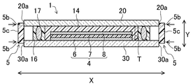
図1、図2に示す様に、有機EL表示装置1は、第1基板である素子基板30と、素子基板30に対向する第2基板である封止基板20と、素子基板30上に形成されるとともに、素子基板30及び封止基板20の間に設けられた有機EL素子4とを備えている。
また、有機EL表示装置1は、有機EL素子4を封止するように素子基板30と封止基板20とを結合(または、溶着)するシール材5を備えている。
このシール材5は、図1、図2に示すように、有機EL表示装置1の面方向X(即ち、有機EL表示装置1の厚み方向Yに直交する方向であって、図1、図2に示す矢印Xの方向)において、封止基板20の外周面20a及び素子基板30の外周面30aに、封止基板20と素子基板30との間を跨ぐように設けられている。
また、本実施形態の有機EL表示装置1においては、図1、図2に示すように、シール材5は、封止基板20の外周面20a及び素子基板30の外周面30aにおいて、有機EL表示装置1を周回するように枠状に形成されており、これにより、有機EL素子4がシール材5により封止される構成となっている。
そして、素子基板30と封止基板20は、シール材5を介して相互に貼り合わされている。素子基板30及び封止基板20は、例えば、ガラス等の絶縁性材料により形成されている。
また、図2に示すように、有機EL素子4は、素子基板30の表面上に設けられた第1電極6(陽極)と、第1電極6の表面上に設けられた有機層7と、有機層7の表面上に設けられた第2電極8(陰極)とを備えている。
第1電極6は、素子基板30の表面上に所定の間隔でマトリクス状に複数形成されており、複数の第1電極6の各々が、有機EL表示装置1の各画素領域を構成している。
なお、本実施形態における素子基板30は、各画素領域ごとにTFT(不図示)を有するアクティブマトリクス基板であり、各画素ごとに設けられたTFTにより各画素ごとにスイッチングを行う構成となっている。
また、第1電極6は、例えば、Au、Ni、Pt、ITO(インジウム-スズ酸化物)、またはITOとAgの積層膜等により形成されている。
有機層7は、マトリクス状に区画された各第1電極6の表面上に形成されている。この有機層7は、図3に示すように、正孔注入層9と、正孔注入層9の表面上に形成された正孔輸送層10と、正孔輸送層10の表面上に形成され、赤色光、緑色光、および青色光のいずれかを発する発光層11と、発光層11の表面上に形成された電子輸送層12と、電子輸送層12の表面上に形成された電子注入層13とを備えている。そして、これらの正孔注入層9、正孔輸送層10、発光層11、電子輸送層12、および電子注入層13が順次積層されることにより、有機層7が構成されている。
正孔注入層9は、発光層11への正孔注入効率を高めるためのものである。この正孔注入層9を形成する材料としては、例えば、ベンジン、スチリルアミン、トリフェニルアミン、ポルフィリン、トリアゾール、イミダゾール、オキサジアゾール、ポリアリールアルカン、フェニレンジアミン、アリールアミン、オキザゾール、アントラセン、フルオレノン、ヒドラゾン、スチルベン、トリフェニレン、アザトリフェニレン、あるいはこれらの誘導体、または、ポリシラン系化合物、ビニルカルバゾール系化合物、チオフェン系化合物あるいはアニリン系化合物等の複素環式共役系のモノマー、オリゴマーあるいはポリマーを挙げることができる。
正孔輸送層10は、上述の正孔注入層9と同様に、発光層11への正孔注入効率を高めるためのものであり、正孔輸送層10を形成する材料としては、上述の正孔注入層9と同様のものが使用できる。
発光層11は、第1電極6、及び第2電極8による電圧印加の際に、両電極の各々から正孔および電子が注入されるとともに、正孔と電子が再結合する領域である。この発光層11は、発光効率が高い材料により形成され、例えば、低分子蛍光色素、蛍光性の高分子、金属錯体等の有機材料により形成されている。より具体的には、例えば、アントラセン、ナフタレン、インデン、フェナントレン、ピレン、ナフタセン、トリフェニレン、アントラセン、ペリレン、ピセン、フルオランテン、アセフェナントリレン、ペンタフェン、ペンタセン、コロネン、ブタジエン、クマリン、アクリジン、スチルベン、あるいはこれらの誘導体、トリス(8-キノリノラト)アルミニウム錯体、ビス(ベンゾキノリノラト)ベリリウム錯体、トリ(ジベンゾイルメチル)フェナントロリンユーロピウム錯体ジトルイルビニルビフェニルが挙げられる。
電子輸送層12は、第2電極8から注入される電子を発光層11に輸送するためのものである。この電子輸送層12を形成する材料としては、例えば、キノリン、ペリレン、フェナントロリン、ビススチリル、ピラジン、トリアゾール、オキサゾール、オキサジアゾール、フルオレノン、またはこれらの誘導体や金属錯体が挙げられる。より具体的には、トリス(8-ヒドロキシキノリン)アルミニウム、アントラセン、ナフタレン、フェナントレン、ピレン、アントラセン、ペリレン、ブタジエン、クマリン、アクリジン、スチルベン、1,10-フェナントロリンまたはこれらの誘導体や金属錯体が挙げられる。
電子注入層13は、上述の電子輸送層12と同様に、第2電極8から注入される電子を発光層11に輸送するためのものであり、電子注入層13を形成する材料としては、上述の電子輸送層12と同様のものが使用できる。
第2電極8は、有機層7に電子を注入する機能を有するものである。この第2電極8は、例えば、マグネシウム合金(MgAg等)、アルミニウム合金(AlLi、AlCa、AlMg等)、金属カルシウム、または仕事関数の小さい金属等により形成されている。
シール材5は、フリットガラス(低融点ガラス)からなり、外気中の水分や酸素を遮断する機能を有するものである。また、フリットガラスとしては、例えば、SiO2(酸化シリコン)、B2O3(酸化ホウ素)、Al2O3(酸化アルミニウム)、V2O5(酸化バナジウム)、CuO(酸化銅)等からなる酸化物の混合ガラスを粉砕して微粉化したものが使用できる。
また、有機EL表示装置1は、図2に示すように、樹脂により形成された樹脂部材14を備えている。この樹脂部材14、フリットガラスにより形成されたシール材5を使用した有機EL表示装置1の機械的強度を向上させるためのものである。樹脂部材14を形成する樹脂としては、例えば、アクリル樹脂、エポキシ樹脂等の紫外線硬化性樹脂や熱硬化性樹脂を使用する構成としている。
また、有機EL表示装置1は、図2に示すように、素子基板30と封止基板20との間に、樹脂により形成された樹脂枠16が設けられている。
この樹脂枠16は、図1に示すように、有機EL素子4を周回するように枠状に形成されている。
樹脂枠16を形成する樹脂材料としては、特に限定されず、安価かつ汎用性のある樹脂材料を使用することができ、例えば、エポキシ樹脂やアクリル樹脂等を使用することができる。なお、これらの樹脂のうち、アクリル樹脂を使用することにより、より一層安価に樹脂枠16を形成することができるため、好ましい。
また、図2に示すように、樹脂枠16には、樹脂部材14の厚みを規制するためのスペーサ17が混入されている。このスペーサ17は、例えば、SiO2(酸化シリコン)により形成されている。
そして、このような樹脂により形成された樹脂枠16を設けることにより、樹脂部材14を、液晶材料の注入方式として採用されている滴下注入方式により形成することが可能になる。
一般に、液晶表示パネルにおいては、一対の基板の間に封入される液晶材料を注入する方法として、真空注入方式と滴下注入方式がある。このうち、滴下注入方式においては、例えば、TFT基板の周囲において、シール材を枠状に形成し、真空雰囲気において、このシール材の枠内のTFT基板上に液晶材料を滴下するとともに、液晶材料が滴下されたTFT基板とCF基板とを貼り合わせる。次いで、基板を大気中に戻し、貼り合わされたTFT基板とCF基板との間の液晶材料を大気圧により拡散させる。そして、紫外光をシール材に照射し、シール材を硬化させて、液晶表示パネルを製造する。
この滴下注入方式は、従来、広く使用されてきた真空注入方式に比し、液晶層の厚みを小さく形成でき、液晶材料の使用量を大幅に低減できるとともに、液晶材料の注入時間を短縮できるため、液晶表示パネルの製造コストを低減させるとともに量産性を向上させることができる。
ここで、液晶材料の滴下注入方式においては、低粘度材料である液晶材料を滴下注入するが、本実施形態における樹脂部材14を形成する樹脂材料の滴下注入方式においては、液晶材料に比し、高粘度材料である樹脂材料を滴下注入するため、真空雰囲気下において、素子基板30と封止基板20を貼り合わせる際に、加圧しなければ滴下注入された樹脂材料が拡散しないという問題が生じる。
そして、そのためには、樹脂材料が存在する貼り合わせ基板の内部の真空状態を保持する必要がある。そこで、上述のごとく、素子基板30と封止基板20との間に、樹脂により形成された樹脂枠16を設ける構成としている。
このような構成により、柔軟性のある樹脂により形成された樹脂枠16が、上述の貼り合わせ基板の内部の真空状態を保持するための圧力隔壁として機能するため、樹脂部材14を形成する滴下注入された樹脂材料が存在する貼り合わせ基板の内部の真空状態を保持することが可能になる。従って、液晶材料に比し、高粘度材料である樹脂材料を滴下注入した場合であっても、真空雰囲気下において、素子基板30と封止基板20を貼り合わせる際に、加圧により滴下注入された樹脂材料を拡散させることが可能になる。
即ち、このような樹脂により形成された樹脂枠16を設けることにより、樹脂により形成された樹脂部材14を滴下注入方式により形成することが可能になる。
そして、滴下注入方式を使用することにより、厚みT(図2参照)の小さい(例えば、3μm以上20μm以下)樹脂部材14を形成することが可能になり、樹脂部材14を薄くすることができる。従って、大型の有機EL表示装置(例えば、幅が265mm以上、長さが200mm以上、厚みが0.3mm以上~0.7mm以下の有機EL表示装置)においても、樹脂部材14を形成する樹脂材料の使用量を減少させることができる。その結果、コストアップを抑制することが可能になる。
なお、樹脂部材14の厚みTは、5μm以上15μm以下が好ましく、6μm以上8μm以下がより好ましい。
次に、本実施形態の有機EL表示装置の製造方法の一例について説明する。図4~図12は、本発明の第1の実施形態に係る有機EL表示装置の製造方法を説明するための図である。
<有機EL素子形成工程>
まず、図4に示すように、基板サイズが300×400mmで、厚さが0.7mmのガラス基板等の素子基板30上に、スパッタ法によりITO膜をパターン形成して、第1電極6を形成する。このとき、第1電極6の膜厚は、例えば、150nm程度に形成する。
まず、図4に示すように、基板サイズが300×400mmで、厚さが0.7mmのガラス基板等の素子基板30上に、スパッタ法によりITO膜をパターン形成して、第1電極6を形成する。このとき、第1電極6の膜厚は、例えば、150nm程度に形成する。
次に、第1電極6上に、発光層11を含む有機層7、及び第2電極8を金属製のマスクを使用して、蒸着法により形成する。
より具体的には、まず、第1電極6を備えた素子基板30を蒸着装置のチャンバー内に設置する。なお、蒸着装置のチャンバー内は、真空ポンプにより、1×10⁻⁵~1×10⁻⁴(Pa)の真空度に保たれている。また、第1電極6を備えた素子基板30は、チャンバー内に取り付けられた1対の基板受けによって2辺を固定した状態で設置する。
そして、蒸着源から、正孔注入層9、正孔輸送層10、発光層11、電子輸送層12、および電子注入層13の各蒸着材料を順次蒸発させて、正孔注入層9、正孔輸送層10、発光層11、電子輸送層12、および電子注入層13を積層することにより、図5に示すように、画素領域に有機層7を形成する。
そして、図6に示すように、有機層7上に、第2電極8を形成することにより、素子基板30上に、第1電極6、有機層7、及び第2電極8を備えた有機EL素子4を形成する。
なお、蒸発源としては、例えば、各蒸発材料が仕込まれた坩堝を使用することができる。坩堝は、チャンバー内の下部に設置されるとともに、坩堝にはヒーターが備え付けられており、このヒーターにより、坩堝は加熱される。そして、ヒーターによる加熱により、坩堝の内部温度が各種蒸着材料の蒸発温度に到達することで、坩堝内に仕込まれた各種蒸着材料が蒸発分子となってチャンバー内の上方向へ飛び出す。
また、有機層7、及び第2電極8の形成方法の具体例としては、まず、素子基板30上にパターニングされた第1電極6上に、RGB全ての画素に共通して、m-MTDATA(4,4,4-tris(3-methylphenylphenylamino)triphenylamine)からなる正孔注入層9を、マスクを介して、例えば、25nmの膜厚で形成する。続いて、正孔注入層9上に、RGB全ての画素に共通して、α-NPD(4,4-bis(N-1-naphthyl-N-phenylamino)biphenyl)からなる正孔輸送層10を、マスクを介して、例えば、30nmの膜厚で形成する。次に、赤色の発光層11として、ジ(2-ナフチル)アントラセン(ADN)に2,6-ビス((4’-メトキシジフェニルアミノ)スチリル)-1,5-ジシアノナフタレン(BSN)を30重量%混合したものを、マスクを介して、画素領域に形成された正孔輸送層10上に、例えば、30nmの膜厚で形成する。次いで、緑色の発光層11として、ADNにクマリン6を5重量%混合したものを、マスクを介して、画素領域に形成された正孔輸送層10上に、例えば、30nmの膜厚で形成する。次に、青色の発光層11として、ADNに4,4’-ビス(2-{4-(N,N-ジフェニルアミノ)フェニル}ビニル)ビフェニル(DPAVBi)を2.5重量%混合したものを、マスクを介して、画素領域に形成された正孔輸送層10上に、例えば、30nmの膜厚で形成する。次いで、各発光層11上に、RGB全ての画素に共通して、8-ヒドロキシキノリンアルミニウム(Alq3)を電子輸送層12として、マスクを介して、例えば、20nmの膜厚で形成する。次いで、電子輸送層12上に、フッ化リチウム(LiF)を電子注入層13として、マスクを介して、例えば、0.3nmの膜厚で形成する。そして、第2電極8として、マグネシウム銀(MgAg)からなる陰極を、例えば、10nmの膜厚で形成する。
<樹脂枠形成工程>
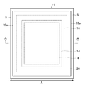
次いで、図7に示すように、例えば、ディスペンサを用いて、基板サイズが95×95mmで、厚さが0.7mmのガラス基板等の封止基板20に、アクリル樹脂、エポキシ樹脂等の紫外線硬化性樹脂や熱硬化性樹脂により構成された樹脂枠16を枠状に描画して形成する。
次いで、図7に示すように、例えば、ディスペンサを用いて、基板サイズが95×95mmで、厚さが0.7mmのガラス基板等の封止基板20に、アクリル樹脂、エポキシ樹脂等の紫外線硬化性樹脂や熱硬化性樹脂により構成された樹脂枠16を枠状に描画して形成する。
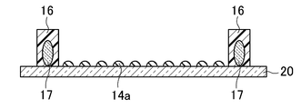
この際、樹脂枠16として、高粘度(100~1000Pa・s)を有するものを形成する。また、上述のごとく、樹脂枠16には、樹脂部材14の厚みを規制するためのスペーサ17が混入されている。
<滴下注入工程(樹脂材料形成工程)>
次いで、図7に示すように、封止基板20に形成された樹脂枠16の内側に、樹脂部材14を形成するための樹脂材料14aを滴下して注入する。なお、樹脂材料14aとしては、例えば、アクリル樹脂、エポキシ樹脂等の紫外線硬化性樹脂が使用される。また、樹脂材料14aの滴下は、例えば、樹脂材料14aを滴下する機能を有した滴下装置が基板面全体に亘って移動しながら樹脂材料14aを滴下することにより行われる。
次いで、図7に示すように、封止基板20に形成された樹脂枠16の内側に、樹脂部材14を形成するための樹脂材料14aを滴下して注入する。なお、樹脂材料14aとしては、例えば、アクリル樹脂、エポキシ樹脂等の紫外線硬化性樹脂が使用される。また、樹脂材料14aの滴下は、例えば、樹脂材料14aを滴下する機能を有した滴下装置が基板面全体に亘って移動しながら樹脂材料14aを滴下することにより行われる。
<貼合体形成工程>
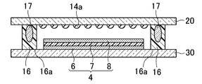
次いで、真空雰囲気で、樹脂材料14aが滴下された封止基板20と、有機EL素子4が形成された素子基板30とを、有機EL素子4と樹脂材料14aが重なり合うように、素子基板30上に封止基板20を重ね合わせて、図8に示すように、素子基板30上に、封止基板20に形成された樹脂枠16の表面16aを載置させる。
次いで、真空雰囲気で、樹脂材料14aが滴下された封止基板20と、有機EL素子4が形成された素子基板30とを、有機EL素子4と樹脂材料14aが重なり合うように、素子基板30上に封止基板20を重ね合わせて、図8に示すように、素子基板30上に、封止基板20に形成された樹脂枠16の表面16aを載置させる。
次いで、図9に示すように、真空雰囲気で、所定の条件下(例えば、100Pa以下の圧力)において、真空気密状態を保持した状態で、窒素リークを行うとともに、大気圧までパージを行って差圧で加圧処理を行うことにより、樹脂枠16の内側において、樹脂材料14aを均一に拡散させ、当該樹脂材料14aを介して、素子基板30と封止基板20とを貼り合わせ、素子基板30と封止基板20とが貼り合わされた貼合体を形成する。
<樹脂硬化工程>
次いで、図10に示すように、封止基板20側から紫外線(図10における矢印)を照射することにより、均一に拡散した樹脂材料14aを硬化させて、樹脂部材14を形成する。
次いで、図10に示すように、封止基板20側から紫外線(図10における矢印)を照射することにより、均一に拡散した樹脂材料14aを硬化させて、樹脂部材14を形成する。
なお、照射する紫外線は、0.5~10Jが好ましく、1~6Jがより好ましい。また、紫外線照射後、大気中にて加熱処理(70℃以上120℃以下、10分以上2時間以下)を行う。
<シール材形成工程>
本実施形態においては、シール材形成工程は、ペースト材料塗布工程と、ペースト材料加熱工程とにより構成される。
本実施形態においては、シール材形成工程は、ペースト材料塗布工程と、ペースト材料加熱工程とにより構成される。
<ペースト材料塗布工程>
まず、図11に示すように、有機EL表示装置1の面方向Yにおける封止基板20の外周面20a及び素子基板30の外周面30aに、有機溶媒(例えば、ブチルカルビトールアセテート)にフリットガラスを加えたペースト材料5aを、封止基板20と素子基板30との間を跨ぐように、ディスペンサやスクリーン印刷法等により塗布して、ペースト材料5aにより有機EL素子4を封止する。
まず、図11に示すように、有機EL表示装置1の面方向Yにおける封止基板20の外周面20a及び素子基板30の外周面30aに、有機溶媒(例えば、ブチルカルビトールアセテート)にフリットガラスを加えたペースト材料5aを、封止基板20と素子基板30との間を跨ぐように、ディスペンサやスクリーン印刷法等により塗布して、ペースト材料5aにより有機EL素子4を封止する。
<ペースト材料加熱工程>
次いで、塗布したペースト材料5aを加熱して焼成することにより、有機溶媒を気化させて、フリットガラスからなり、有機EL素子4を封止するシール材5を、封止基板20の外周面20a及び素子基板30の外周面30aにおいて、有機EL表示装置1を周回するように枠状に形成する。
次いで、塗布したペースト材料5aを加熱して焼成することにより、有機溶媒を気化させて、フリットガラスからなり、有機EL素子4を封止するシール材5を、封止基板20の外周面20a及び素子基板30の外周面30aにおいて、有機EL表示装置1を周回するように枠状に形成する。
このように、加熱により、フリットガラスからなるシール材5を形成することにより、シール材5により、素子基板30と封止基板20とが固定されることになる。
なお、焼成する際の加熱温度は、200℃以上500℃以下が好ましく、250℃以上400℃以下がより好ましい。これは、焼成において、ペースト材料5aにおける有機溶媒を完全に除去しなければ、本焼成において、アウトガスの要因となり、後述するフリットガラスからなるシール材5による溶着の妨げとなるためである。
<溶着工程>
次いで、図12に示すように、シール材5に対して、YAGレーザー等のレーザー光源を用いてレーザー光(図12における矢印)を照射することにより、フリットガラスからなるシール材5のみを選択的に加熱して、シール材5により素子基板30と封止基板20との間を溶着する。
次いで、図12に示すように、シール材5に対して、YAGレーザー等のレーザー光源を用いてレーザー光(図12における矢印)を照射することにより、フリットガラスからなるシール材5のみを選択的に加熱して、シール材5により素子基板30と封止基板20との間を溶着する。
ここで、本実施形態においては、フリットガラスからなるシール材5に対して、当該シール材5の全体を加熱するのではなく、シール材5の一部のみに対してレーザー光を照射することにより加熱して、非照射領域を設ける構成としている。このような構成により、熱伝搬による有機EL素子4へのダメージを低減することが可能になる。
より具体的には、図12に示すように、シール材5の、封止基板20の外周面20a及び素子基板30の外周面30aと接触する部分5bのみを選択的に加熱することにより、シール材5により素子基板30と封止基板20との間を溶着する。
このような溶着方法により、上記従来技術とは異なり、シール材5の全体に対してレーザー照射を行うことなく、素子基板30と封止基板20との間を溶着することができるため、レーザー加熱に起因する熱伝搬による有機EL素子4へのダメージを低減することができる。
より具体的には、シール材5において、封止基板20の外周面20a及び素子基板30の外周面30aと接触する部分5b以外の部分(即ち、非照射領域)5cは、レーザー照射による加熱が行われないため、この非照射領域5cが放熱作用を有することになる。
そして、このように、シール材5において、加熱しない非照射領域5cが存在することになるため、シール材5の熱容量が増加し、シール材5の内部における温度上昇が回避できる。
従って、レーザー光Lの照射に伴うシール材5の温度上昇が、有機EL素子4に物理的に伝搬されることを効果的に抑制することが可能になるため、レーザー加熱に起因する熱伝搬による有機EL素子4へのダメージを低減することができる。
また、上述のごとく、素子基板30はTFTを備えているが、有機EL素子4と同様に、レーザー加熱に起因する熱伝搬によるダメージを低減することができるため、TFTの配線パターンとシール材5との距離を大きくする必要がなくなる。従って、レーザー加熱に起因する熱伝搬によるダメージを避けるために、シール材5とTFTとの間を離間させる必要がなくなるため、有機EL表示装置1を小型化することが可能になる。
また、上述のごとく、溶着を行う前に、加熱により、フリットガラスからなるシール材を形成して、シール材5により、素子基板30と封止基板20とを固定しているため、レーザー照射による溶着を行う際に、素子基板30及び封止基板20の移動を防止することができる。従って、レーザー照射による溶着を行う際の素子基板30と封止基板20のズレの発生を防止して、有機EL表示装置1の歩留まりの低下を防止することができる。
なお、図13に示す、照射するレーザー光Lのスポット径r(即ち、溶着幅)は、0.1mm以上1mm以下が好ましく、0.1mm以上0.5mm以下がより好ましい。これは、スポット径rが1mmより大きい場合は、レーザー光Lの照射エリアが有機EL素子4に近づくため、レーザー加熱に起因する熱伝搬による有機EL素子4へのダメージの低減効果が低下する場合があるためである。また、スポット径rが0.1mmよりも小さい場合は、レーザー照射による溶着が不十分になり、シール材5による外気中の水分や酸素を遮断する機能が十分に発揮されない場合があるためである。
また、この場合、例えば、YAGレーザー(λ=1.06μm)を50~200Wの出力で使用し、ファイバーレーザーで口径を0.1~1mm径に絞り込み、ガラスを通して、シール材5の、封止基板20の外周面20a及び素子基板30の外周面30aと接触する部分5bにレーザーを照射する。そして、レーザー光源であるYAGレーザー、または加工対象であるシール材5を駆動させて、シール材5を形成するフリットガラスを加熱、溶融して、素子基板30と封止基板20との間の溶着を行う。
以上に説明した本実施形態によれば、以下の効果を得ることができる。
(1)本実施形態においては、溶着を行う前に、封止基板20の外周面20a及び素子基板30の外周面30aに、有機溶媒にフリットガラスを加えたペースト材料5aを、封止基板20と素子基板30との間を跨ぐように塗布して、ペースト材料5aにより有機EL素子4を封止し、このペースト材料5aを加熱して焼成することにより、有機溶媒を気化させて、フリットガラスからなるシール材5を形成する構成としている。従って、レーザー照射による溶着を行う際に、素子基板30及び封止基板20の移動を防止することができるため、レーザー照射による溶着を行う際の素子基板30と封止基板20のズレの発生を防止し、有機EL表示装置1の歩留まりの低下を防止することができる。
(2)本実施形態においては、シール材5の、封止基板20の外周面20a及び素子基板30の外周面30aと接触する部分5bのみをレーザー照射により加熱して、シール材5により封止基板20と素子基板30との間を溶着する構成としている。従って、シール材5の全体に対してレーザー照射を行うことなく、素子基板30と封止基板20との間を溶着することができるため、レーザー加熱に起因する熱伝搬による有機EL素子4へのダメージを低減することができる。
(3)本実施形態においては、溶着工程において、レーザー光のスポット径rを0.1mm以上1mm以下に設定する構成としている。従って、レーザー加熱に起因する熱伝搬による有機EL素子4へのダメージの低減効果を低下させることなく、シール材5により外気中の水分や酸素を遮断することができる。
(4)本実施形態においては、真空雰囲気で、樹脂枠16の内側において、樹脂材料14aを均一に拡散させ、樹脂材料14aを介して、封止基板20と素子基板30とを貼り合わせた後、樹脂材料14aを硬化させて樹脂部材14を形成する構成としている。従って、樹脂枠16が、封止基板20と素子基板30による貼り合わせ基板の内部の真空状態を保持するための圧力隔壁として機能するため、樹脂部材14を滴下注入方式により形成することが可能になる。その結果、厚みの小さいの樹脂部材14を形成することが可能になり、樹脂部材14を薄くすることができるため、大型の有機EL表示装置1においても、樹脂部材14を形成する樹脂材料14aの使用量を減少させることができる。その結果、コストアップを抑制することが可能になる。
(5)本実施形態においては、樹脂枠16に、樹脂部材14の厚みを規制するためのスペーサ17を混入する構成としている。従って、樹脂部材14を滴下注入方式により形成する場合であっても、樹脂部材14の厚みを精度良く規制することが可能になる。
(6)本実施形態においては、樹脂枠16を、アクリル樹脂またはエポキシ樹脂により形成する構成としている。従って、安価かつ汎用性のある樹脂材料により樹脂枠16を形成することができる。
(7)本実施形態においては、ペースト材料加熱工程において、ペースト材料5aを焼成する際の加熱温度を200℃以上500℃以下に設定する構成としている。従って、焼成において、ペースト材料5aにおける有機溶媒を完全に除去して、フリットガラスからなるシール材5による溶着を容易に行うことが可能になる。
(第2の実施形態)
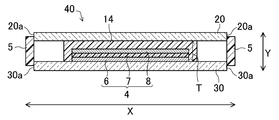
次に、本発明の第2の実施形態について説明する。図14は、本発明の第2の実施形態に係る有機EL表示装置の断面図である。なお、上記第1の実施形態と同様の構成部分については同一の符号を付してその説明を省略する。
次に、本発明の第2の実施形態について説明する。図14は、本発明の第2の実施形態に係る有機EL表示装置の断面図である。なお、上記第1の実施形態と同様の構成部分については同一の符号を付してその説明を省略する。
本実施形態の有機EL表示装置40の製造方法においては、樹脂部材14を形成する樹脂材料として、フィルム状の樹脂材料が使用され、図14に示すように、樹脂枠16が使用されていない点に特徴がある。
第1の実施形態においては、封止基板20に形成された樹脂枠16の内側に、樹脂部材14を形成するための樹脂材料14aを滴下して注入する滴下注入方式を使用する構成としたが、この滴下注入方式では、上述のごとく、樹脂材料14aが存在する貼り合わせ基板の内部の真空状態を保持するための樹脂枠16を設ける必要がある。
一方、本実施形態のごとく、フィルム状の樹脂材料を使用することにより、真空状態を保持する必要がなくなるため、上記樹脂枠16を設ける必要がなくなり、コストダウンを図ることが可能になる。
また、フィルム状の樹脂材料を使用することにより、樹脂部材14の平坦性が向上し、更に、樹脂材料の使用量をより一層低減することが可能になるため、コストダウンを図ることが可能になる。
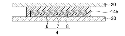
次に、本実施形態の有機EL表示装置の製造方法の一例について説明する。図15~図18は、本発明の第2の実施形態に係る有機EL表示装置の製造方法を説明するための図である。
まず、上述の第1の実施形態の場合と同様に、有機EL素子形成工程により、素子基板30上に、第1電極6、有機層7、及び第2電極8を備えた有機EL素子4を形成する(図6参照)。
<樹脂材料形成工程>
次いで、図15に示すように、封止基板20上に、例えば、ラミネート装置やダイヤフラムを使用して、フィルム状の樹脂材料14bを形成する。この際、処理温度を、例えば、70℃~100℃に設定する。なお、樹脂材料14bとしては、例えば、アクリル樹脂、エポキシ樹脂等の紫外線硬化性樹脂が使用される。また、フィルム状の樹脂材料14bとしては、例えば、3μm~40μmの厚みを有するものが使用できる。
次いで、図15に示すように、封止基板20上に、例えば、ラミネート装置やダイヤフラムを使用して、フィルム状の樹脂材料14bを形成する。この際、処理温度を、例えば、70℃~100℃に設定する。なお、樹脂材料14bとしては、例えば、アクリル樹脂、エポキシ樹脂等の紫外線硬化性樹脂が使用される。また、フィルム状の樹脂材料14bとしては、例えば、3μm~40μmの厚みを有するものが使用できる。
<貼合体形成工程>
次いで、フィルム状の樹脂材料14bが形成された封止基板20と、有機EL素子4が形成された素子基板30とを、有機EL素子4と樹脂材料14bが重なり合うように、素子基板30上に封止基板20を重ね合わせて、図16に示すように、有機EL素子4上に、封止基板20に形成された樹脂材料14bの表面14cを載置させる。
次いで、フィルム状の樹脂材料14bが形成された封止基板20と、有機EL素子4が形成された素子基板30とを、有機EL素子4と樹脂材料14bが重なり合うように、素子基板30上に封止基板20を重ね合わせて、図16に示すように、有機EL素子4上に、封止基板20に形成された樹脂材料14bの表面14cを載置させる。
次いで、図17に示すように、所定の条件下(例えば、転写温度:50℃~85℃、硬化温度:100℃~120℃、処理時間:2時間以内、真空度:200Pa、圧力:3~7N/m2)において、加圧処理を行うことにより、樹脂材料14bを介して、素子基板30と封止基板20とを貼り合わせ、素子基板30と封止基板20とが貼り合わされた貼合体を形成する。
<樹脂硬化工程>
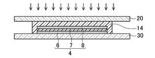
次いで、図18に示すように、封止基板20側から紫外線(図18における矢印)を照射することにより、樹脂材料14bを硬化させて、樹脂部材14を形成する。
次いで、図18に示すように、封止基板20側から紫外線(図18における矢印)を照射することにより、樹脂材料14bを硬化させて、樹脂部材14を形成する。
なお、照射する紫外線は、0.5~10Jが好ましく、1~6Jがより好ましい。また、紫外線照射後、大気中にて加熱処理(70℃以上120℃以下、10分以上2時間以下)を行う。
そして、上述の第1の実施形態の場合と同様に、シール材形成工程を行うことにより、図14に示す有機EL表示装置が製造される。
以上に説明した本実施形態によれば、上述の(1)~(3)、(7)の効果に加えて、以下の効果を得ることができる。
(8)本実施形態においては、フィルム状の樹脂材料14bを使用する構成としている。従って、滴下注入方式と異なり、樹脂材料が存在する貼り合わせ基板の内部の真空状態を保持するための樹脂枠16を設ける必要が無くなるため、コストダウンを図ることが可能になる。
(9)また、フィルム状の樹脂材料14bを使用することにより、樹脂部材14の平坦性が向上する。
(10)更に、フィルム状の樹脂材料14bを使用することにより、樹脂材料の使用量をより一層低減することが可能になり、コストダウンを図ることが可能になる。
なお、上記実施形態は以下のように変更しても良い。
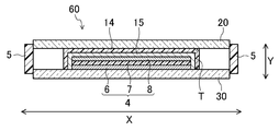
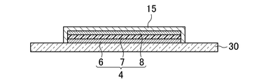
図19、図20に示すように、有機EL素子4と樹脂部材14との接触を防止して、有機EL素子4を保護するための保護膜15を、有機EL素子4の表面上に設ける構成としてもよい。この保護膜15を形成する材料としては、例えば、SiO2、SiON等の無機材料が挙げられる。
また、この場合、上述の有機EL素子形成工程を行った後、図21に示すように、素子基板30上に形成された有機EL素子4の表面上に、当該有機EL素子4を保護するための保護膜15を形成する。この保護膜15は、例えば、SiO2、SiON等の無機材料を、蒸着法、スパッタ法、化学気相成長法等により、有機EL素子4の表面上に積層することにより形成することができる。
その後、上述の第1の実施形態において説明した樹脂枠形成工程、滴下注入工程、貼合体形成工程、樹脂硬化工程、及びシール材形成工程を行うことにより、図19に示す有機EL表示装置50を製造することができる。また、上述の第2の実施形態において説明した樹脂部材貼り付け工程、貼合体形成工程、樹脂硬化工程、及びシール材形成工程を行うことにより、図20に示す有機EL表示装置60を製造することができる。
以上説明したように、本発明は、有機EL素子を備えた有機EL表示装置の製造方法およびその方法により製造された有機EL表示装置に適している。
1 有機EL表示装置
4 有機EL素子
5 シール材
5a ペースト材料
6 第1電極
7 有機層
8 第2電極
14 樹脂部材
14a 樹脂材料
15 保護膜
16 樹脂枠
17 スペーサ
20 封止基板(第2基板)
20a 封止基板の外周面
30 素子基板(第1基板)
30a 素子基板の外周面
40 有機EL表示装置
50 有機EL表示装置
60 有機EL表示装置
L レーザー光
r レーザー光のスポット径
4 有機EL素子
5 シール材
5a ペースト材料
6 第1電極
7 有機層
8 第2電極
14 樹脂部材
14a 樹脂材料
15 保護膜
16 樹脂枠
17 スペーサ
20 封止基板(第2基板)
20a 封止基板の外周面
30 素子基板(第1基板)
30a 素子基板の外周面
40 有機EL表示装置
50 有機EL表示装置
60 有機EL表示装置
L レーザー光
r レーザー光のスポット径
Claims (8)
- 第1基板上に有機EL素子を形成する有機EL素子形成工程と、
第2基板上に樹脂材料を形成する樹脂材料形成工程と、
前記樹脂材料を介して、前記第1基板と前記第2基板とを貼り合わせる貼合体形成工程と、
前記樹脂材料を硬化させて樹脂部材を形成する樹脂硬化工程と、
前記第1基板の外周面及び前記第2基板の外周面に、有機溶媒にフリットガラスを加えたペースト材料を、前記第1基板と前記第2基板との間を跨ぐように塗布して、前記ペースト材料により前記有機EL素子を封止するペースト材料塗布工程と、
前記ペースト材料を加熱して焼成することにより、前記有機溶媒を気化させて、前記フリットガラスからなるシール材を形成するペースト材料加熱工程と、
前記シール材の、前記第1基板の外周面及び前記第2基板の外周面と接触する部分のみをレーザー照射により加熱して、前記シール材により前記第1基板と前記第2基板との間を溶着する溶着工程と
を少なくとも備えることを特徴とする有機EL表示装置の製造方法。 - 前記溶着工程において、レーザー光のスポット径が0.1mm以上1mm以下であることを特徴とする請求項1に記載の有機EL表示装置の製造方法。
- 前記樹脂材料形成工程の前に、前記第2基板に樹脂枠を形成する樹脂枠形成工程を更に備え、
前記樹脂材料形成工程において、前記樹脂枠の内側に、前記樹脂材料を滴下して注入することにより、前記第2基板上に前記樹脂材料を形成し、
前記貼合体形成工程において、真空雰囲気で、前記樹脂枠の内側において、前記樹脂材料を均一に拡散させ、該樹脂材料を介して、前記第1基板と前記第2基板とを貼り合わせることを特徴とする請求項1または請求項2に記載の有機EL表示装置の製造方法。 - 前記樹脂枠には、前記樹脂部材の厚みを規制するスペーサが混入されていることを特徴とする請求項3に記載の有機EL表示装置の製造方法。
- 前記樹脂枠は、アクリル樹脂またはエポキシ樹脂により形成されていることを特徴とする請求項3または請求項4に記載の有機EL表示装置の製造方法。
- 前記樹脂材料形成工程において、フィルム状の樹脂材料を形成することを特徴とする請求項1または請求項2に記載の有機EL表示装置の製造方法。
- 前記ペースト材料加熱工程において、前記ペースト材料を焼成する際の加熱温度が200℃以上500℃以下であることを特徴とする請求項1~請求項6のいずれか1項に記載の有機EL表示装置の製造方法。
- 請求項1~請求項7のいずれか1項に記載の方法により製造された有機EL表示装置。
Applications Claiming Priority (2)
| Application Number | Priority Date | Filing Date | Title |
|---|---|---|---|
| JP2011037840 | 2011-02-24 | ||
| JP2011-037840 | 2011-02-24 |
Publications (1)
| Publication Number | Publication Date |
|---|---|
| WO2012114685A1 true WO2012114685A1 (ja) | 2012-08-30 |
Family
ID=46720481
Family Applications (1)
| Application Number | Title | Priority Date | Filing Date |
|---|---|---|---|
| PCT/JP2012/001029 Ceased WO2012114685A1 (ja) | 2011-02-24 | 2012-02-16 | 有機el表示装置の製造方法およびその方法により製造された有機el表示装置 |
Country Status (1)
| Country | Link |
|---|---|
| WO (1) | WO2012114685A1 (ja) |
Citations (4)
| Publication number | Priority date | Publication date | Assignee | Title |
|---|---|---|---|---|
| JP2003292348A (ja) * | 2001-12-31 | 2003-10-15 | Boe-Hydis Technology Co Ltd | 平板表示素子の基板合着方法 |
| US20060103301A1 (en) * | 2004-11-12 | 2006-05-18 | Eastman Kodak Company | Sealing of organic thin-film light-emitting devices |
| JP2009016185A (ja) * | 2007-07-05 | 2009-01-22 | Panasonic Electric Works Co Ltd | 有機elパネル |
| WO2010143337A1 (ja) * | 2009-06-11 | 2010-12-16 | シャープ株式会社 | 有機el表示装置およびその製造方法 |
-
2012
- 2012-02-16 WO PCT/JP2012/001029 patent/WO2012114685A1/ja not_active Ceased
Patent Citations (4)
| Publication number | Priority date | Publication date | Assignee | Title |
|---|---|---|---|---|
| JP2003292348A (ja) * | 2001-12-31 | 2003-10-15 | Boe-Hydis Technology Co Ltd | 平板表示素子の基板合着方法 |
| US20060103301A1 (en) * | 2004-11-12 | 2006-05-18 | Eastman Kodak Company | Sealing of organic thin-film light-emitting devices |
| JP2009016185A (ja) * | 2007-07-05 | 2009-01-22 | Panasonic Electric Works Co Ltd | 有機elパネル |
| WO2010143337A1 (ja) * | 2009-06-11 | 2010-12-16 | シャープ株式会社 | 有機el表示装置およびその製造方法 |
Similar Documents
| Publication | Publication Date | Title |
|---|---|---|
| US8710492B2 (en) | Organic EL display device and method for manufacturing the same | |
| US20120068169A1 (en) | Organic el display device and method for manufacturing the same | |
| EP2476774B1 (en) | Deposition source and organic layer deposition apparatus including the same | |
| KR101356096B1 (ko) | 반도체장치 및 그의 제작방법 | |
| TWI553133B (zh) | 薄膜沉積裝置及利用其製造薄膜的方法 | |
| US20090220680A1 (en) | Oled device with short reduction | |
| US20120025182A1 (en) | Donor substrate, process for production of transfer film, and process for production of organic electroluminescent element | |
| US9391295B2 (en) | Organic EL display apparatus | |
| JP6429491B2 (ja) | 蒸着装置用マスク、蒸着装置、蒸着方法、及び、有機エレクトロルミネッセンス素子の製造方法 | |
| WO2015163247A1 (ja) | 有機エレクトロルミネッセンス表示装置用基板、有機エレクトロルミネッセンス表示装置、有機エレクトロルミネッセンス表示装置の製造方法、及び、有機エレクトロルミネッセンス表示装置の製造装置 | |
| JP2013187019A (ja) | 有機el表示装置およびその製造方法 | |
| CN104347665B (zh) | 制造有机发光显示设备的方法 | |
| JP2011054477A (ja) | 有機エレクトロルミネッセンス表示装置、および有機エレクトロルミネッセンス表示装置の製造方法 | |
| WO2012063445A1 (ja) | 有機el表示装置およびその製造方法 | |
| KR102120896B1 (ko) | 대향 타겟 스퍼터링 장치를 이용한 유기발광표시장치 및 그 제조방법 | |
| WO2013150713A1 (ja) | 有機el表示装置およびその製造方法 | |
| WO2012114685A1 (ja) | 有機el表示装置の製造方法およびその方法により製造された有機el表示装置 | |
| WO2012093467A1 (ja) | 有機el表示装置およびその製造方法 | |
| KR20150012541A (ko) | 대향 타겟 스퍼터링 장치, 이를 이용한 유기발광표시장치 및 그 제조방법 |
Legal Events
| Date | Code | Title | Description |
|---|---|---|---|
| 121 | Ep: the epo has been informed by wipo that ep was designated in this application |
Ref document number: 12749949 Country of ref document: EP Kind code of ref document: A1 |
|
| NENP | Non-entry into the national phase |
Ref country code: DE |
|
| 122 | Ep: pct application non-entry in european phase |
Ref document number: 12749949 Country of ref document: EP Kind code of ref document: A1 |
|
| NENP | Non-entry into the national phase |
Ref country code: JP |