WO2012108378A1 - 表面プラズモン共鳴測定用チップ - Google Patents
表面プラズモン共鳴測定用チップ Download PDFInfo
- Publication number
- WO2012108378A1 WO2012108378A1 PCT/JP2012/052604 JP2012052604W WO2012108378A1 WO 2012108378 A1 WO2012108378 A1 WO 2012108378A1 JP 2012052604 W JP2012052604 W JP 2012052604W WO 2012108378 A1 WO2012108378 A1 WO 2012108378A1
- Authority
- WO
- WIPO (PCT)
- Prior art keywords
- film
- alloy film
- plasmon resonance
- surface plasmon
- layer region
- Prior art date
- Legal status (The legal status is an assumption and is not a legal conclusion. Google has not performed a legal analysis and makes no representation as to the accuracy of the status listed.)
- Ceased
Links
Images


Classifications
-
- G—PHYSICS
- G01—MEASURING; TESTING
- G01N—INVESTIGATING OR ANALYSING MATERIALS BY DETERMINING THEIR CHEMICAL OR PHYSICAL PROPERTIES
- G01N21/00—Investigating or analysing materials by the use of optical means, i.e. using sub-millimetre waves, infrared, visible or ultraviolet light
- G01N21/17—Systems in which incident light is modified in accordance with the properties of the material investigated
- G01N21/55—Specular reflectivity
- G01N21/552—Attenuated total reflection
- G01N21/553—Attenuated total reflection and using surface plasmons
-
- G—PHYSICS
- G01—MEASURING; TESTING
- G01N—INVESTIGATING OR ANALYSING MATERIALS BY DETERMINING THEIR CHEMICAL OR PHYSICAL PROPERTIES
- G01N33/00—Investigating or analysing materials by specific methods not covered by groups G01N1/00 - G01N31/00
- G01N33/48—Biological material, e.g. blood, urine; Haemocytometers
- G01N33/50—Chemical analysis of biological material, e.g. blood, urine; Testing involving biospecific ligand binding methods; Immunological testing
- G01N33/53—Immunoassay; Biospecific binding assay; Materials therefor
- G01N33/543—Immunoassay; Biospecific binding assay; Materials therefor with an insoluble carrier for immobilising immunochemicals
- G01N33/551—Immunoassay; Biospecific binding assay; Materials therefor with an insoluble carrier for immobilising immunochemicals the carrier being inorganic
- G01N33/553—Metal or metal coated
Definitions
- the present invention relates to a chip for surface plasmon resonance measurement, and more particularly to a chip for surface plasmon resonance measurement using an Ag alloy thin film.
- SPR Surface Plasmon Resonance Sensor
- SPR phenomenon is an SPR measurement chip such as a prism on which a metal thin film is vapor-deposited.
- SPR phenomenon is a phenomenon in which surface plasmons are resonantly excited on the surface of the metal thin film due to an evanescent wave generated when incident light is irradiated under total reflection conditions (SPR phenomenon).
- the SPR phenomenon depends on the incident angle and wavelength of incident light incident on the metal thin film, and surface plasmons are resonantly excited at a constant incident angle or wavelength.
- the incident angle and wavelength at which the surface plasmon is excited vary depending on the state of the substance existing on the surface of the metal thin film, and the reflected light intensity reflected from the metal thin film decreases. Therefore, SPR measurement techniques for measuring and analyzing the bond strength and bond speed between molecules based on the amount of change in reflected light intensity are used in various fields such as applied physics, biochemistry, and biology.
- a ligand (a substance that specifically binds to a detection sample such as a protein) is immobilized on a metal thin film of an SPR measurement chip, and the detection is performed on the surface of the chip.
- a sample is prepared and incident light is applied to the metal thin film.
- the state of the metal thin film surface changes due to the reaction between the ligand and the detection sample, so by measuring the change in the resonance angle and the resonance wavelength (decrease in reflected light intensity) A desired detection sample can be measured with high sensitivity.
- an SPR measurement chip is composed of a transparent dielectric substrate, a metal thin film, and a thin film having a ligand capable of immobilizing a substance to be detected in order from the substrate side.
- SPR measurement chips are roughly classified into a prism type having a prism that totally reflects a specific light source wavelength and a diffraction grating type using a substrate on which a diffraction grating is formed without using a prism.
- pure Au or pure Ag is usually used as the metal thin film used for the SPR measurement chip.
- a metal thin film (Au film) using pure Au is generally used because it has excellent chemical resistance against chemicals adhering to the detection object (for example, halogen-based substances such as NaCl and alkaline substances).
- the detection object for example, halogen-based substances such as NaCl and alkaline substances.
- the SPR measurement chip is disposable, the SPR measurement chip using the Au film has a problem that the running cost becomes high.
- the light source wavelength that can be used for the Au film is limited to red to near-infrared, detection objects that can be measured by SPR are limited to those that can be measured within that range.
- a metal thin film (Ag film) using a pure Ag film is lower in cost than an Au film, can use a wavelength in the visible light region, and has high resonance characteristics in the wavelength region.
- the Ag film has low stability with respect to NaCl, its use range is limited, and improvement in halogen resistance has been demanded.
- Patent Document 1 proposes a chip for SPR measurement in which stability against NaCl is improved by adding a noble metal such as Au to Ag.
- a noble metal such as Au
- high-temperature heat treatment such as PCR reaction (polymerase chain reaction) is performed on the substrate, the crystal grains of the noble metal-Ag film are coarsened and the surface smoothness deteriorates, resulting in resonance characteristics. Since it tends to decrease, measurement is difficult particularly when the measurement area of the detected object is a very small area.
- Patent Document 2 also discloses that oxidation resistance of Ag is improved by adding at least one selected from Au, Pt, Cu, Bi, Nd, Ti, and Sb to Ag in an amount of 0.05 mol% or more and less than 10 mol%. Improvement techniques have been proposed. However, the technique described in Patent Document 2 only discloses an improvement in oxidation resistance (preservability) against oxygen and water in the air, and suggests any solution to the above problems at the time of use. It has not been done. In addition, when only Au or the like is contained, the halogen resistance is insufficient, such as aggregation of the Ag alloy film due to contact with halogen or deterioration of SPR characteristics.
- the present invention has been made in view of the above situation, and has an object of having excellent resonance characteristics (initial half-value width), being capable of using a wide range of light source wavelengths, and being excellent in resistance.
- An object of the present invention is to provide an SPR measuring chip having halogenity (Ag aggregation resistance, light reflectance after halogen contact).
- the present invention that has achieved the above object is a surface plasmon resonance measuring chip in which an Ag alloy film containing Bi is formed on a transparent dielectric substrate, and the Bi content in the vicinity of the surface of the Ag alloy film Is a surface plasmon resonance measuring chip having a gist that a Bi concentrated layer region higher than the Bi content of the entire Ag alloy film is formed.
- the average thickness of the Bi concentrated layer region is 0.1 to 10 nm.
- the Ag alloy film further contains at least one selected from the group consisting of Ge, Au, Cu, and Sn.
- the Ag alloy film contains 0.2 to 3 atomic% of Bi and the balance is made of Ag and inevitable impurities.
- the Ag alloy film contains 0.2 to 2 atomic% of Bi, 0.1 to 1 atomic% of at least one selected from the group consisting of Ge, Au, Cu, and Sn, with the balance being Ag. It is also a preferred embodiment that it consists of unavoidable impurities.
- the Ag alloy film is formed on the transparent dielectric substrate directly or via a transparent oxide conductive film or an intervening layer not containing Cu.
- the transparent dielectric substrate is bismuth oxide glass.
- a diffraction grating microstructure is provided on at least one surface of the transparent dielectric substrate.
- the SPR measurement chip of the present invention having an Ag alloy film in which a Bi-concentrated layer region is formed in the vicinity of the surface only has excellent resonance characteristics equivalent to those of a conventional SPR measurement chip using an Au film.
- the entire visible light region can be used as the light source wavelength, and it has excellent halogen resistance. Therefore, the SPR measurement chip of the present invention can measure a wider range of samples than the conventional Au film as a detection object.
- a detection object in the biological field containing NaCl even if NaCl and an Ag alloy film are in contact with each other, aggregation of Ag and a decrease in reflected light intensity can be suppressed and measurement can be performed with high sensitivity.
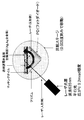
- FIG. 1 is a schematic explanatory diagram of SPR measurement used in the examples.
- FIG. 2 is a graph showing a resonance curve in Example 1.
- FIG. 3 is a graph showing the RBS analysis results of the test pieces used in Examples 3 and 4.
- FIG. 4 is a graph showing the relationship between the thickness of the Bi concentrated layer region and the full width at half maximum.
- FIG. 5 is a graph showing the relationship between the thickness of the Bi concentrated layer region and the reflectance.
- the present inventors have intensively studied to solve the above problems. As a result, it is an Ag alloy film containing Bi as a metal thin film used for the SPR measurement chip, and the Bi concentration in the vicinity of the surface of the Ag alloy film is higher than the Bi content of the entire Ag alloy film. If the layer region is formed, it has excellent resonance characteristics comparable to those of an Au film for a light source (for example, laser) having a wide range of wavelengths (entire visible light), and has a high level of halogen resistance exceeding that of a pure Ag film. As a result, the present invention was completed.
- a light source for example, laser
- “excellent in resonance characteristics (SPR characteristics)” means that the SPR measurement chip is irradiated with a light source such as a laser having a certain wavelength to measure the reflected light intensity, the vertical axis represents the reflected light intensity, When a resonance curve is drawn with the horizontal axis as the incident angle, it means that it has a half-value width equivalent to Au. That is, the initial half width is high.
- the half-value width (initial half-value width) of the Ag alloy film of the present invention is preferably within 80%, more preferably within 50% of the half-value width of Au.
- the angle of the resonance curve is within 0.7 °, more preferably within 0.5 °.
- Halogen resistance refers to Ag aggregation resistance when the Ag alloy film is in contact with halogen (hereinafter sometimes referred to as corrosion resistance), and a decrease in light reflectance after the halogen contact (amount of change in half width) is suppressed. That satisfies both of the requirements (hereinafter sometimes referred to as durability).
- Near the surface means to include a predetermined thickness (substrate direction) from the outermost surface of the Ag alloy film, and as described later, for example, a depth from the outermost surface to 0.1 to 10 nm, The region where the Bi concentrated layer region is formed from the RBS analysis result.
- the SPR measurement chip using a pure Ag film is expected to be used because it is cheaper than Au and has a wide usable light source wavelength.
- Ag atoms easily diffuse and aggregate due to the influence of chlorine ions. Changes in the surface of the thin film due to such aggregation caused a decrease in resonance characteristics.
- aggregation or the like occurs in a metal thin film used as a reflection film for SPR measurement, there is a problem that the influence on reflected light intensity is large, the resonance characteristics are remarkably deteriorated, and the measurement accuracy is lowered. Therefore, a pure Ag film cannot be used for a sample to which sodium chloride is adhered, such as a biological member, and its use range is extremely limited.
- the SPR measuring chip using the Bi-containing Ag alloy film of the present invention can use a wide range of light source wavelengths as in the case of pure Ag, and the experimental result that the resonance characteristic has the same level as Au. Obtained.
- the Bi concentration contained in the entire Ag alloy film is high, the Bi concentrated layer region is not formed, and Bi is uniformly dispersed throughout the Ag alloy film (that is, in the film). Sex cannot be obtained.
- the reflected light intensity decreased and the SPR characteristics deteriorated as the Bi concentration increased.
- this tendency depends on the state of Bi in the vicinity of the surface of the Ag alloy film.
- the amount of oxide (particularly Bi 2 O 3 ) constituting the Bi concentrated layer region increases, the halogen resistance is further improved and the reflected light is reflected. A decrease in strength is also suppressed. Accordingly, it is desirable that the amount of Bi uniformly dispersed throughout the Ag alloy film is small, and that the amount of Bi existing as an oxide is large in the vicinity of the Ag alloy film surface (that is, a Bi concentrated layer is formed). Is desirable).
- the thickness of the Bi concentrated layer region is preferably 0.1 to 10 nm from the outermost surface of the Ag alloy film. For example, as shown in FIGS. 4 and 5, if the Bi-concentrated layer region becomes too thick, the half-value width (initial half-value width) becomes wide, and the SPR characteristics deteriorate (both Ag-1 in FIG. 4 and FIG. 5). .5 atomic% Bi target used). When the Bi concentrated layer region is too thick as described above, desired SPR characteristics cannot be obtained. Therefore, the thickness is preferably 10 nm or less, more preferably 5 nm or less, and further preferably 2 nm or less. On the other hand, if the Bi-concentrated layer region is too thin, sufficient halogen resistance as a protective film cannot be obtained. Therefore, it is preferably 0.1 nm or more, more preferably 0.2 nm or more, and further preferably 0.4 nm or more. To do.
- the Bi-concentrated layer region is within the specific range (within 10 nm from the outermost surface) in the inner direction of the Ag alloy film (substrate side) from the outermost surface of the Ag alloy film (the side opposite to the substrate side).
- the Bi concentration is 10 times higher.
- the measurement of such a Bi concentrated layer region can be calculated by quantifying the Bi content in the film thickness direction using RBS (Rutherford Bachscattering Spectrometry).
- the average Bi content of the entire Ag alloy film can be measured by ICP emission analysis.
- the Bi content is preferably 0.2 atomic% or more, more preferably 0.5 atomic% or more. It is desirable to do. This is because when the Bi content is small, the above-described effects due to the addition of Bi cannot be sufficiently obtained.
- the upper limit of Bi content is not particularly defined, but in order to ensure resonance characteristics, the upper limit of Bi content is preferably 3 atomic%. Addition of Bi to Ag tends to lower the reflected light intensity. This tendency becomes more prominent as the Bi content increases, and as a result, the resonance characteristics of the Bi-containing Ag alloy film may be lowered. When the Bi content exceeds 3 atomic%, the resonance characteristics are lowered with a decrease in reflected light intensity. A more preferable upper limit of the Bi content is 1.5 atomic%.
- the Ag alloy used in the present invention preferably contains Bi as described above, and the balance is Ag and inevitable impurities.
- the Bi concentrated layer region is formed on the surface layer side of the Ag alloy film.
- the Bi concentrated layer is not necessarily formed uniformly, and pinholes or the like may occur. In such a case, halogen, water, or the like that has passed through the Bi concentrated layer region through the pinhole may come into contact with Ag to aggregate Ag.
- the addition of the above elements eliminates these problems.
- Ge, Au, Cu, and Sn diffuse into the Ag alloy film, suppress aggregation of Ag atoms due to contact with a halogen compound such as NaCl contained together with the detection object, and are effective in improving halogen resistance.
- a halogen compound such as NaCl contained together with the detection object
- Cu and Sn are effective in improving sulfidation resistance in addition to halogen resistance.
- the content of Ge, Au, Cu, and Sn (single content in the case of single, and total amount when including two or more) is 0.1 atomic% or more and 1 atomic% or less. It is preferable. This is because if the content is less than 0.1 atomic%, an effective effect due to the addition of the above elements cannot be obtained, and if the content exceeds 1 atomic%, the reflected light intensity decreases and desired resonance characteristics cannot be obtained.
- the lower limit of the more preferable content is 0.4 atomic% or more, and the upper limit is 0.8 atomic% or less.
- the Bi content is desirably decreased according to the contents of Ge, Au, Cu, and Sn.
- Bi is preferably 2 atom% or less, more preferably 1.0 atom% or less.
- the minimum of Bi content is not specifically limited, As mentioned above, it is preferable to make it contain 0.2 atomic% or more, More preferably, it is 0.5 atomic% or more.
- the thickness of the Bi-containing Ag alloy film is not particularly limited, and may be a desired film thickness according to the type of SPR measurement chip. However, if the film thickness is too thin, incident light may pass through the Bi-containing Ag alloy film, and the reflected light intensity may decrease. Further, from the viewpoint of ensuring a stable film formation by uniformly forming the film, the thickness is preferably 30 nm or more. From the viewpoint of ensuring the above SPR characteristics at the refractive index of a normal substrate (about 1.4 to 2.2), the film thickness is recommended to be 40 nm or more. However, even if the film thickness is increased, the effect of improving the above characteristics is saturated while the cost increases. Further, from the viewpoint of securing SPR characteristics in the refractive index of the substrate, the film thickness is preferably 100 nm or less, more preferably 80 nm or less.
- a method for forming a Bi-containing Ag alloy film or the like for example, a vapor deposition method, a sputtering method, an ion plating method, an electroplating method, or the like is well known.
- a vapor deposition method for example, a vapor deposition method, a sputtering method, an ion plating method, an electroplating method, or the like is well known.
- a sputtering method In order to form a Bi concentrated layer region having a high Bi content in the vicinity of the surface, it is desirable to use a sputtering method. This is because the sputtering method is excellent for forming a thin film having excellent in-film uniformity and film thickness uniformity of components.
- the specific discharge voltage varies depending on other manufacturing conditions such as gas pressure and Bi content, but is preferably 15 (W) or more, more preferably 30 (W) or more, and preferably 150 (W ) Or less, more preferably 100 (W) or less.
- the thickness of the Bi concentrated layer region can be grown and the amount of Bi contained in the Bi concentrated layer region can be increased.
- the specific gas pressure during film formation varies depending on other manufacturing conditions such as a discharge voltage and Bi content, but is preferably 2 mTorr or more, more preferably 3 mTorr or more, still more preferably 4 mTorr or more, and still more preferably. 5 mTorr or more, preferably 8 mTorr or less, more preferably 6 mTorr or less.
- an inert atmosphere gas such as Ar as a gas during film formation.
- the Bi-concentrated layer region can be formed by an Ag-Bi sputtering target. Further, in order to form a thick Bi-concentrated layer region (for example, 2 nm or more), it is desirable to chip-on Bi to the Ag sputtering target or to form a film by co-sputtering with the Bi sputtering target.
- the transparent dielectric substrate in the SPR measurement chip of the present invention is not particularly limited as long as it is a transparent material that transmits laser, and optical glass or synthetic resin that is generally used for SPR measurement is used. it can.
- the optical glass include various optical glasses
- examples of the synthetic resin include various resins such as an acrylic resin, a polycarbonate resin, a polystyrene resin, and an epoxy resin.
- bismuth oxide glass As the optical glass, it is preferable to use bismuth oxide glass as the optical glass.
- the inventors have improved the corrosion resistance. Turned out to be.
- the reason why the excellent corrosion resistance is exhibited when the Bi-containing Ag alloy film is formed on the bismuth oxide glass is unknown in detail, but it seems that bismuth oxide in the glass acts to suppress Ag aggregation.
- the bismuth oxide glass used in the present invention refers to a glass containing bismuth oxide (Bi 2 O 3 ).
- bismuth oxide-based glass has an effect of suppressing defects caused by pinhole defects even when pinholes are generated in the Bi-containing Ag alloy film, and can exhibit sufficient halogen resistance. That is, when a material other than bismuth oxide glass is used as a substrate, if a pin pole is generated in the Bi-containing Ag alloy film as described above, the pin hole becomes a defect and sufficient halogen resistance cannot be obtained. When bismuth oxide glass is used, sufficient halogen resistance can be exhibited even if there is a pinhole defect. However, when a film containing Cr as an intervening layer (intervening layer) is used between the bismuth oxide-based glass substrate and the Bi-containing Ag alloy film, Ag may diffuse into Cr, leading to deterioration of characteristics.
- intervening layer an intervening layer
- the transparent dielectric substrate used in the present invention may have a concavo-convex (grating) diffraction grating on the surface.
- the diffraction grating may be formed on at least one surface (at least the surface irradiated with light) of the substrate.
- a diffraction grating type SPR measurement chip using a substrate having a diffraction grating can be manufactured at a low cost, and it is not necessary to use a prism. Therefore, a measurement value caused by variation in the degree of adhesion between the prism and the transparent dielectric substrate. Can be suppressed.
- a transparent dielectric substrate having a diffraction grating is preferable because there are less restrictions on the light source such as a laser diameter and a beam irradiation position as compared with the case of using a prism.
- the structure of the diffraction grating is not particularly limited, a fine structure having a period (400 nm) or less in which the average surface roughness (about 4 nm) of the pure Ag film reaches 1% of the structure of the diffraction grating is preferable, and more preferably 10 nm.
- the microstructure is 200 nm or less.
- the resonance condition depends on the structure of the substrate surface. Therefore, in order to effectively exert the resonance effect based on the structural design, the state that accurately reflects the structure of the substrate surface It is desirable to form a metal thin film.
- the Bi-containing Ag alloy film is used, film formation along the uneven shape on the substrate surface is easy.
- the film surface after film formation has advantages such as excellent smoothness. In particular, since the Bi-containing Ag alloy film maintains the smoothness of the film surface even after the heat treatment, it has excellent resonance characteristics and can be used for various detection objects. Low running costs can be achieved.
- the SPR measurement chip of the present invention is not limited to the diffraction grating type as described above, and a prism type including a prism may be used.
- the prism used in the present invention is not particularly limited as long as it is normally used for SPR measurement.
- a Bi-containing Ag alloy film is laminated on the transparent dielectric substrate.
- the Bi-containing Ag alloy film may be directly laminated on the transparent dielectric substrate, or depending on the required characteristics of the SPR measurement chip, the transparent dielectric is within the range that does not impair the operation of the present invention.
- Another layer may be interposed between the substrate and the Bi-containing Ag alloy film.
- a transparent oxide conductive film such as ITO (Indium Tin Oxide) or IZO (Indium Zinc Oxide) is used as an intervening layer (intermediate layer) for the purpose of enhancing properties such as adhesion between the transparent dielectric substrate and the Bi-containing Ag alloy film. You may provide as.
- the transparent oxide conductive film is desirable because it has good adhesion to the Ag alloy film and has high light transmittance.
- Such a configuration in which the intervening layer is provided is preferably applied particularly when the Kretschmann arrangement is adopted as the SPR measurement method.
- the thickness of the intervening layer may be appropriately set in relation to the Bi-containing Ag alloy film so that a desired adhesion effect can be obtained.
- the thickness of the intervening layer is too thick, for example, the amount of Ag diffused in the intervening layer increases and the reflected light intensity is reduced, so the thickness is preferably 200 nm or less.
- the intervening layer is used, if the film thickness is too thin, the effect of improving the adhesion by the transparent conductive film may not be sufficiently obtained. If it is in the said film thickness range, the transmittance
- general-purpose Cr is not used as the intervening layer.
- Cr has been used because it exhibits an excellent effect in improving the adhesion between the substrate and the Ag alloy film.
- Ag is contained in Cr. This is because not only the reflected light intensity is diffused and the reflected light intensity is lowered, but also the halogen resistance is deteriorated as shown in Examples below.
- a ligand or the like can be fixed or other layers can be laminated according to the type of SPR measurement chip.
- the SPR measurement chip of the present invention can be used in various known SPR measurement devices, and can be used in various fields such as lighting, communication, analysis, chemistry, and biotechnology.
- the prism type SPR measurement shown in FIG. 1 was simulated.
- the reflected light intensity was calculated based on a known multiple reflection calculation formula. Specifically, the multiple reflection calculation formula described in Biosensor Chemical Sensor Dictionary First Edition (page 135, issued in 2007: Techno System Co., Ltd.) was referred to.
- the film thickness of the Ag alloy film a sample for film thickness measurement was prepared at the time of sample preparation, and the measured value measured with a contact-type step gauge (deck tack) was taken as the film thickness.
- a target material (diameter: 4 inch, thickness: 5 mm) on an oxidized Bi-containing glass substrate (Bi 2 O 3 glass: K-Psfn3 manufactured by Sumita Optical Glass Co.) or a glass substrate not containing oxidized Bi (HOYA: FD60)
- the film was formed by sputtering using Ag-1.0 atomic% Bi (No. 1 to 4, 8 to 11) or Ag-1.5 atomic% Bi (No. 5 to 7) as The balance of the target is Ag and inevitable impurities).
- a Cr film having a thickness of 1.2 nm (No. 8) or an ITO film having a thickness of 200 nm (Nos. 6 and 7) was formed on the substrate as an intervening layer.
- the Cr film was formed by using a magnetron DC sputtering apparatus manufactured by Shimadzu Corporation under the conditions of a film forming power of 50 W and an Ar gas pressure of 2 mTorr.
- the film was formed below.
- Reference Example A pure Au chip (manufactured by GE Healthcare: SIA Kit, a half-value width of 1.5 ° for a wavelength of 635 nm, a film thickness of 55 nm; a theoretical value of a half-value width of 0.9 °) was adopted as a reference value for comparison and reference. .
- the theoretical value was calculated based on “Optical thin film and film formation technology” (Agne Technical Center, ULVAC translation, first edition, page 447). Similarly, the theoretical value reference value 0.2 ° of the half width calculated based on the same document was adopted as the reference value of the pure Ag film.
- a substrate is placed on a BK7 prism (BK is a borosilicate crown, the refractive index is 1.514 for a wavelength of 635 nm) fixed on a rotating stage via pure water (refractive index 1.41), and collimated to a spread angle of 1 mrad or less.
- the laser beam (wavelength 635 nm) is incident at an angle of 38.8 ° when viewed from the prism horizontal plane, and the reflected light is received by a PD (photodiode) while rotating the prism in increments of 0.025 °.
- the reflected light intensity up to ° was plotted.
- Each test piece was compared with the half width of the pure Au chip to evaluate whether it had an initial half width equivalent to Au.
- Corrosion resistance (Ag aggregation resistance) is determined by immersing each specimen in a 50 mM NaCl aqueous solution, immediately washing with pure water, further immersing in pure water for 15 minutes and drying, and then clouding the Ag alloy film of the specimen. It was examined by confirming whether or not this occurred. The case where white turbidity occurred was evaluated as “not present”, and the case where white turbidity did not occur was evaluated as “no”, and was described in the “Presence of white turbidity” column in the table.
- Figure 2 shows experiment no. It is the figure which plotted the half value width (initial half value width and process latter half value width) before and behind immersion of 1 50 mM NaCl aqueous solution.
- the thickness of the concentrated layer region is less than 0.1 nm from the outermost surface of the Ag alloy film: ⁇ , 0.1 to 10 nm: ⁇ , more than 10 nm: ⁇ , and even when the thickness is 0.1 to 10 nm, the film is not uniform ( In the case of pinhole), it was evaluated as ⁇ and described in the “Bi concentrated layer region” column in the table. The presence or absence of pinholes was judged by observing the surface of the Ag alloy film with SEM.
- Table 1 shows the following. First, no. Nos. 1 to 7 and 9 are examples of the present invention. Nos. 2 to 7 and 9 have excellent halogen resistance, corrosion resistance (no cloudiness), durability (half-value width variation), and excellent SPR characteristics (initial half-value width) almost equivalent to those of Au films. Had. In addition, No. No. 1 had pinholes in the Ag alloy film due to the relatively low gas pressure, but No. 1 uses oxidized Bi-based glass as the substrate. Although it was inferior to 2-7 and 9, it was excellent in SPR characteristics, corrosion resistance and durability.
- No. 8, 10, and 11 are comparative examples.
- No. No. 8 had pin holes in the Ag alloy film because the gas pressure was relatively low.
- No. No. 8 is No. Similar to 1, oxide Bi-based glass was used as a substrate, but since Cr was formed as an intervening layer, defects due to pinholes could not be suppressed and the corrosion resistance was poor.
- No. No. 10 had a relatively low gas pressure, and on the other hand, increased film deposition power, so the Bi-concentrated layer region could not be formed thick and the corrosion resistance was poor.
- No. No. 11 had a pinhole due to its relatively low gas pressure. No. In No. 11, defects caused by pinholes could not be suppressed, and the corrosion resistance was poor.
- the Ag alloy film preferably has no pinholes (Nos. 2 to 7, 9). Moreover, even when there is a pinhole, the defect due to the pinhole defect can be suppressed by using the oxidized Bi-based glass substrate (No. 1), but even when the oxidized Ni-based glass is used, Cr When forming as an intervening layer, the desired effect cannot be obtained (No. 8). On the other hand, when the gas pressure is relatively low, pinholes tend to be formed (Nos. 1, 8, and 11), and when the deposition power is increased, a sufficiently thick Bi concentrated layer region cannot be formed. (No. 10)
- the following consideration is based on the trend of the conditions of this example, and the specific preferable numerical range can vary depending on the experimental conditions.
- the experiment was performed by controlling both the Ar gas pressure and the film formation power during the sputtering film formation within the preferable range of the present invention.
- the following considerations examine the tendency of a more suitable range for obtaining the Bi concentrated layer region and preferable characteristics even within the range.
- No. 10 is also No. 10. This is an example in which the film formation power is higher than that of No. 11, and it is considered that Bi is gasified and released during film formation.
- No. No. 8 was No. except that a Cr film was formed as an intervening layer.
- an Ag alloy film was formed in the same manner as in Example 1, but it was considered that Ag was clouded because Cr was provided as an intervening layer even when oxidized Bi-based glass that suppresses Ag aggregation was used.
Landscapes
- Health & Medical Sciences (AREA)
- Immunology (AREA)
- Life Sciences & Earth Sciences (AREA)
- Chemical & Material Sciences (AREA)
- Engineering & Computer Science (AREA)
- Physics & Mathematics (AREA)
- Analytical Chemistry (AREA)
- Pathology (AREA)
- General Physics & Mathematics (AREA)
- Hematology (AREA)
- Biomedical Technology (AREA)
- Molecular Biology (AREA)
- Urology & Nephrology (AREA)
- General Health & Medical Sciences (AREA)
- Biochemistry (AREA)
- Microbiology (AREA)
- Inorganic Chemistry (AREA)
- Medicinal Chemistry (AREA)
- Food Science & Technology (AREA)
- Cell Biology (AREA)
- Biotechnology (AREA)
- Investigating Or Analysing Materials By Optical Means (AREA)
Abstract
本発明の目的は優れた耐ハロゲン性を有し、且つ反射光強度の低減が抑制されてAu膜と同等の反射光強度を備えたAg合金膜を使用した表面プラズモン共鳴測定用チップを提供すること。本発明は、透明誘電体基板の上に、Biを含むAg合金膜が形成された表面プラズモン共鳴測定用チップであって、前記Ag合金膜の表面近傍におけるBi含有率が、前記Ag合金膜全体のBi含有率よりも高いBi濃化層領域が形成されていることに要旨を有する。
Description
本発明は、表面プラズモン共鳴測定用チップに関し、詳細にはAg合金薄膜を用いた表面プラズモン共鳴測定用チップに関するものである。
表面プラズモン共鳴(Surface Plasmon Resonance Sensor:以下、「SPR」と略記することがある。)とは、金属薄膜を蒸着したプリズムなどのSPR測定用チップにおいて、SPR測定用チップのプリズム側から金属薄膜に対して全反射条件にて入射光を照射したときに生じるエバネッセント波に起因して、金属薄膜表面に表面プラズモンが共鳴して励起される現象である(SPR現象)。SPR現象は、金属薄膜に入射される入射光の入射角や波長に依存しており、一定の入射角または波長のときに表面プラズモンが共鳴励起される。表面プラズモンが励起される入射角や波長は、金属薄膜の表面に存在する物質の状態によって変化し、金属薄膜から反射される反射光強度が減少する。そのため、反射光強度の変化量によって分子間の結合強度や結合速度などを測定、解析するSPR測定技術が、応用物理、生化学、生物学などの様々な分野で利用されている。
例えば、生化学分野においてタンパク質等の検出試料を検出する場合、SPR測定用チップの金属薄膜上にリガンド(タンパク質等の検出試料と特異的に結合する物質)を固定し、このチップの表面に検出試料を配置したものを用意しておき、金属薄膜に対して入射光を照射する。目的となる検出試料が存在する場合、リガンドと検出試料とが反応して金属薄膜表面の状態が変化するため、共鳴角や共鳴波長の変化(反射光強度の減少量)を測定することにより、所望とする検出試料を高感度で測定することができる。
一般にSPR測定用チップは、基板側から順に、透明誘電体基板と、金属薄膜と、検出対象となる物質を固定化できるリガンドなどを有する薄膜とから構成されている。
SPR測定用チップは、特定の光源波長を全反射させるプリズムを有するプリズム型と、プリズムを使わずに回折格子が形成された基板を用いる回折格子型に大別される。
SPR測定用チップに使用される金属薄膜として、通常、純Auや純Agが用いられている。
このうち純Auを用いた金属薄膜(Au膜)は、検出物に付着している薬品類(例えばNaClなどのハロゲン系物質やアルカリ性物質)に対する耐薬品性に優れているため、一般的に使用されている。しかしながらSPR測定用チップは使い捨てであるため、Au膜を使用したSPR測定用チップはランニングコストが高くなるという問題があった。またAu膜に対して使用できる光源波長は赤色~近赤外に限定されるため、SPRで測定できる検出物もその範囲で測定できるものに限られていた。
これに対し、純Ag膜を用いた金属薄膜(Ag膜)は、Au膜に比べて低コストであると共に、可視光領域の波長を使用でき、しかもその波長領域での共鳴特性が高い。もっともAg膜はNaClに対する安定性が低いことから、その使用範囲が限られており、耐ハロゲン性の向上が求められていた。
そこで、このような問題を解決する技術として特許文献1には、AgにAuなどの貴金属を添加することによってNaClに対する安定性を向上させたSPR測定用チップが提案されている。しかしながら、特許文献1に記載の技術では、貴金属の添加によって純Ag膜が有していた光学特性が変化し、共鳴特性が低下するため、高感度の測定分析を行うことは難しい。また基板上でPCR反応(ポリメラーゼ連鎖反応)のような100℃程度の熱サイクルを被る高温熱処理を行うと、貴金属-Ag膜の結晶粒が粗大化して表面平滑性が悪化して、共鳴特性が低下する傾向があるため、特に検出物の測定領域が微小領域である場合には測定が難しい。
また特許文献2には、AgにAu、Pt、Cu、Bi、Nd、Ti、Sbから選ばれる少なくとも一種を0.05モル%以上10モル%未満で添加することによって、Agの耐酸化性を向上させる技術が提案されている。しなしながら、特許文献2に記載の技術では、空気中の酸素や水に対する耐酸化性(保存性)の向上について開示があるのみで、使用時における上記問題点に対する解決策は何ら開示も示唆もされていない。また単にAu等を含有させただけでは、ハロゲンとの接触によってAg合金膜が凝集したり、SPR特性が悪化するなど、耐ハロゲン性は不十分であった。
本発明は上記のような状況に鑑みてなされたものであって、その目的は優れた共鳴特性(初期半値幅)を有し、且つ広範な光源波長の利用が可能であると共に、優れた耐ハロゲン性(耐Ag凝集性、ハロゲン接触後の光反射率)を備えたSPR測定用チップを提供することにある。
上記課題を達成し得た本発明は、透明誘電体基板の上に、Biを含むAg合金膜が形成された表面プラズモン共鳴測定用チップであって、前記Ag合金膜の表面近傍におけるBi含有率が、前記Ag合金膜全体のBi含有率よりも高いBi濃化層領域が形成されていることに要旨を有する表面プラズモン共鳴測定用チップである。
本発明では、前記Bi濃化層領域の平均厚さは、0.1~10nmであることも好ましい実施態様である。
また本発明では、前記Ag合金膜は更にGe、Au、Cu、およびSnよりなる群から選択される少なくとも一種を含むものであることも好ましい実施態様である。
更に本発明では、前記Ag合金膜はBiを0.2~3原子%含有し、残部がAg及び不可避的不純物からなることも好ましい実施態様である。
本発明では、前記Ag合金膜はBiを0.2~2原子%、Ge、Au、Cu、およびSnよりなる群から選択される少なくとも一種を0.1~1原子%含有し、残部がAg及び不可避的不純物からなることも好ましい実施態様である。
また本発明では、前記Ag合金膜は、直接、あるいは透明酸化物導電膜、またはCuを含まない介在層を介して透明誘電体基板に形成されたものであることも好ましい実施態様である。
更に本発明では、前記透明誘電体基板が酸化ビスマス系ガラスであることも好ましい実施態様である。
また更に本発明では、前記透明誘電体基板の少なくとも一方の面に回折格子状微細構造が設けられていることも好ましい実施態様である。
Bi濃化層領域が表面近傍に形成されているAg合金膜を備えた本発明のSPR測定用チップは、従来のAu膜を使用したSPR測定用チップと同等の優れた共鳴特性を有するだけでなく、光源波長として可視光全域を使用できると共に、優れた耐ハロゲン性を有する。したがって本発明のSPR測定用チップは、検出物として従来のAu膜よりも広範な試料を測定することができる。特にNaClが含まれる生物分野の検出物についてもNaClとAg合金膜が接触しても、Agの凝集や反射光強度の低下を抑制でき、感度よく測定することができる。
上記本発明のSPR測定用チップを用いれば、低コストで高精度の分析を行うことができる。
本発明者らは、上記問題を解決すべく、鋭意検討を重ねてきた。その結果、SPR測定用チップに用いられる金属薄膜としてBiを含有するAg合金膜であって、Ag合金膜の表面近傍におけるBi含有率が、Ag合金膜全体のBi含有率よりも高いBi濃化層領域が形成されていれば、広範な波長(可視光全域)の光源(例えばレーザ)に対してAu膜に匹敵する優れた共鳴特性を有すると共に、純Ag膜を凌駕する高レベルの耐ハロゲン性を発揮することを見出し、本発明を完成した。
本発明において「共鳴特性(SPR特性)に優れている」とは、SPR測定用チップに一定の波長を有するレーザなどの光源を照射して反射光強度を測定し、縦軸を反射光強度、横軸を入射角度として共鳴曲線を描いたとき、Auと同等の半値幅を有することを意味する。すなわち、初期半値幅が高いことである。
ここで、「Auと同等の半値幅を有する」とは、本発明のAg合金膜の半値幅(初期半値幅)がAuの半値幅の好ましくは80%以内、より好ましくは50%以内にあること、或いは共鳴曲線の角度が0.7°以内、より好ましくは0.5°以内にあることを意味する。
耐ハロゲン性とは、Ag合金膜がハロゲンと接触した場合の耐Ag凝集性(以下、耐食性ということがある)と、ハロゲン接触後の光反射率の低下(半値幅の変化量)が抑制されていること(以下、耐久性ということがある)の両方を満足するものをいう。
「表面近傍」とは、Ag合金膜の最表面から所定の厚み(基板方向)を含む意味であって、後記するように、例えば最表面から0.1~10nmまでの深さであって、RBS分析結果からBi濃化層領域が形成されている領域をいう。
以下、本発明について詳細に説明する。
前述したように純Ag膜を用いたSPR測定用チップは、Auに比べて安価であり、また使用可能な光源波長が広いことから、その活用が期待されていた。しかしながらAg原子は塩素イオンの影響によって容易に拡散・凝集することが知られていた。こうした凝集に起因する薄膜表面の変化は共鳴特性の低下を引き起こしていた。特にSPR測定用の反射膜として使用される金属薄膜に凝集等が生じると、反射光強度への影響が大きく、共鳴特性を著しく劣化させ、測定精度が低下するという問題があった。したがって生体部材など塩化ナトリウムが付着している試料については純Ag膜を使用することができず、その利用範囲は極く限られたものとなっていた。
そこで本発明者らが鋭意研究を重ねた結果、SPR測定用チップに用いられる金属薄膜として、Ag合金膜全体のBi含有率(平均Bi濃度)よりも高いBi含有率を有する濃化層領域がAg合金膜表面近傍に形成されているBi含有Ag合金膜を用いれば、上記問題を見事に解決できることを見出した。このようなBi濃化層領域が形成されたBi含有Ag合金膜の形成によって上記特性が発揮される理由として、Bi含有Ag合金膜の成膜時に、加熱により生成したBi酸化物が膜表面に濃化してBi酸化物濃化層が形成され、このBi酸化物濃化層によって耐ハロゲン性が向上すると推察される。
上記したようにBi濃化層領域を形成すると、濃化層以外の領域では、相対的にBi濃度(含有率)が低くなり、純Agに近い高反射率を維持できる。したがって本発明のBi含有Ag合金膜を用いたSPR測定用チップは、純Agと同様に広範な光源波長の使用が可能であり、また共鳴特性についてはAuと同等のレベルを有するという実験結果も得られた。
一方でAg合金膜全体に含まれるBi濃度が高くても、Bi濃化層領域が形成されずに、Ag合金膜全体(すなわち、膜中)にBiが均一に分散している場合、耐ハロゲン性が得られない。またBi濃度が高くなるにつれて反射光強度が低下してSPR特性も悪くなることが確認された。もっともこうした傾向はAg合金膜の表面近傍のBiの状態によっても左右され、Bi濃化層領域を構成する酸化物量(特にBi2O3)が多いほど耐ハロゲン性が一層向上すると共に、反射光強度の低下も抑制される。したがってAg合金膜全体に均一に分散するBi量は少ないほうが望ましく、またAg合金膜表面近傍は酸化物として存在しているBi量が多いことが望ましい(すなわち、Bi濃化層が形成されていることが望ましい)。
Bi濃化層領域の厚さは、Ag合金膜最表面から0.1~10nmであることが望ましい。例えば図4、図5に示すように、Bi濃化層領域が厚くなりすぎると、半値幅(初期半値幅)が広くなり、SPR特性が悪化する(図4、図5のいずれもAg-1.5原子%Biターゲットを使用)。このようにBi濃化層領域が厚すぎると、所望のSPR特性が得られなくなるため、好ましくは10nm以下、より好ましくは5nm以下、更に好ましくは2nm以下とする。一方、Bi濃化層領域が薄すぎると、保護膜として十分な耐ハロゲン性を得ることができないため、好ましくは0.1nm以上、より好ましくは0.2nm以上、更に好ましくは0.4nm以上とする。
なお、Bi濃化層領域とは、Ag合金膜の最表面(基板側とは反対側)からAg合金膜膜内部方向(基板側)のうち、上記特定の範囲内(最表面から10nm以内)におけるBi濃度が、Ag合金膜全体におけるBi含有率(平均含有率)よりも高い領域をいう。例えば上記Bi濃度が10倍以上高いことが望ましい。特にBi濃化層領域にピンホールがなく、かつBiがBi濃化層領域内で均一に分散しているものが好ましい。
このようなBi濃化層領域(層厚)の測定は、RBS(Rutherford Bachscattering Spectrometry)を用いて、膜厚方向のBi含有量を定量化することによって算出することができる。またAg合金膜全体の平均Bi含有率は、ICP発光分析法で測定することができる。
本発明ではAg合金膜にBiを添加しているが、耐ハロゲン性を確保するという観点からは、Bi含有量は、好ましくは0.2原子%以上、より好ましくは0.5原子%以上とすることが望ましい。Bi含有量が少ないとBi添加による上記効果が十分に得られないからである。一方、耐ハロゲン性向上という観点からは、Bi含有量の上限は特に規定されないが、共鳴特性を確保するには、Bi含有量の上限は3原子%とすることが好ましい。AgへのBi添加は、反射光強度を低下させる傾向がある。この傾向はBi含有量が増加するにつれて顕著となり、結果としてBi含有Ag合金膜の共鳴特性を低下させることがある。Bi含有量が3原子%を超えると、反射光強度の低下に伴って共鳴特性が低下する。より好ましいBi含有量の上限は1.5原子%である。
本発明に用いられるAg合金は、上記のようにBiを含み、残部はAgおよび不可避的不純物であることが好ましい。
なお、本発明では、Bi含有Ag合金の上記特性を一層向上させる目的で、更にGe、Au、Cu、およびSnよりなる群から選択される少なくとも一種を含有させることも有効である。本発明ではAg合金膜の表層側にBi濃化層領域を形成しているが、Bi濃化層が均一に形成されているとは限らず、ピンホール等が生じている場合もある。このような場合、ピンホールを通じてBi濃化層領域を通過したハロゲンや水などが、Agと接触してAgを凝集させることがある。しかし上記元素の添加により、これらの問題は解消される。
すなわち、Ge、Au、Cu、およびSnは、Ag合金膜中に拡散し、検出物と共に含まれるNaClなどのハロゲン化合物との接触によるAg原子の凝集を抑制し、耐ハロゲン性向上に有効である。これらの中でもCuとSnは耐ハロゲン性に加えて耐硫化性向上にも有効である。
Ge、Au、Cu、およびSnの含有量(単独の場合は単独の含有量であり、2種以上を含むときは合計量である)は、0.1原子%以上、1原子%以下とすることが好ましい。0.1原子%未満では、上記元素の添加による有効な効果が得られず、含有量が1原子%を超えると反射光強度が低下し、所望の共鳴特性が得られないからである。より好ましい含有量の下限は0.4原子%以上であって、上限は0.8原子%以下である。
またGe、Au、Cu、およびSnよりなる群から選択される少なくとも一種の元素を添加する場合、これらの元素を含まない場合に比べてAg合金膜中のBi含有量を低減させることが好ましい。Ag合金膜に含まれる合金元素の合計量が増加すると、共鳴特性が低下するからである。したがって、Bi含有量はGe、Au、Cu、およびSnの含有量に応じて低下させることが望ましく、例えばBiは2原子%以下とすることが好ましく、より好ましくは1.0原子%以下である。なお、Bi含有量の下限は特に限定されず、上記したように0.2原子%以上含有させるのが好ましく、より好ましくは0.5原子%以上である。
Bi含有Ag合金膜の厚さは特に限定されず、SPR測定用チップの種類などに応じて所望の膜厚とすればよい。しかし膜厚が薄すぎると入射光がBi含有Ag合金膜を透過してしまい、反射光強度が低下することがある。また膜を均一に形成して安定した上記特性を確保する観点からは、好ましくは30nm以上とする。また通常の基板の屈折率(1.4~2.2程度)において上記SPR特性を確保する観点からは、膜厚は40nm以上とすることが推奨される。ただし、膜厚を厚くしても上記特性の向上効果が飽和する一方でコストが上昇する。また上記基板の屈折率においてSPR特性を確保する観点からは、膜厚は好ましくは100nm以下、より好ましくは80nm以下である。
Bi含有Ag合金膜等の成膜方法として例えば、蒸着法、スパッタリング法、イオンプレーティング法、電気メッキ法などが通常用いられる成膜方法として公知であるが、本発明のようにAg合金膜の表面近傍におけるBi含有率が高いBi濃化層領域を形成するには、スパッタリング法によることが望ましい。スパッタリング法は、成分の膜内均一性や膜厚均一性に優れた薄膜の形成に優れているからである。またスパッタリング法による場合は以下に説明するように成膜時に放電電圧(成膜パワー)とガス圧を高めることが必要である。
すなわち、スパッタリング法による成膜においては、基板の表面は二次電子や反跳Arが入射し、その際、実効的な基板温度が上昇してBiが濃化する現象が生じる。そして、この基板表面の温度はスパッタ時の放電電圧と相関があり、高放電電圧ほどこの温度を高くすることができることも分った。これは、高放電電圧のほうが低放電電圧の場合に比べて上記二次電子や反跳Arの入射時のエネルギーが高いことに起因しているものと考えられる。もっとも電圧が高すぎるとBiがガス化してしまいAg合金膜を成膜しても、十分な厚さを有するBi濃化層領域を得ることができない。具体的な放電電圧は、ガス圧などの他の製造条件やBi含有量などによっても異なるが、好ましくは15(W)以上、より好ましくは30(W)以上であって、好ましくは150(W)以下、より好ましくは100(W)以下である。
また成膜時にはガス圧も高めてガス流量を増やすことで、Bi濃化層領域の厚みを成長させてBi濃化層領域に含まれるBi量を増大させることができる。また上記したように放電電圧やBi含有量等の他の製造条件によるが、ガス厚を高めることによって、Bi濃化層領域のピンホールの形成を抑制することができる。具体的な成膜時のガス圧は、放電電圧などの他の製造条件やBi含有量などによっても異なるが、好ましくは2mTorr以上、より好ましくは3mTorr以上、更に好ましくは4mTorr以上、より更に好ましくは5mTorr以上であって、好ましくは8mTorr以下、より好ましくは6mTorr以下である。
また好ましくは成膜時のガスとしてArなどの不活性雰囲気ガスを用いるのがよい。
なお、Bi濃化層領域の形成にあたってはAg-Biスパッタリングターゲットにより成膜することもできる。またBi濃化層領域を厚く(例えば2nm以上)形成するためにはAgスパッタリングターゲットにBiをチップオンしたり、Biスパッタリングターゲットとコスパッタリング法によって成膜することが望ましい。
以上、本発明を最も特徴付けるBi含有Ag合金膜について説明した。
以下、上記Bi含有Ag合金膜を備えた本発明のSPR測定用チップの各構成およびその製造方法について説明するが、本発明は下記構成及び製造方法に限定されず、必要に応じて構成や製造方法に適宜変更を加えることもできる。
本発明のSPR測定用チップにおける透明誘電体基板は、レーザを透過する透明な材料であれば特に限定されず、SPR測定用に一般的に使用されている光学ガラスや合成樹脂などを用いることができる。光学ガラスとしては各種光学ガラスが例示され、合成樹脂としてはアクリル樹脂、ポリカーボネート樹脂、ポリスチレン樹脂、エポキシ樹脂などの各種樹脂が例示される。
本発明では、光学ガラスとして酸化ビスマス系ガラスを用いることが好ましい。本発明者らが、酸化ビスマス系ガラスを用いた場合と、酸化ビスマスを含有していないガラスとで、Bi含有Ag合金膜の耐食性について調べた結果、酸化ビスマス系ガラスを用いると、耐食性が向上することが判明した。Bi含有Ag合金膜を酸化ビスマス系ガラスに形成した場合に優れた耐食性を発揮する理由は詳細には不明であるが、ガラス中の酸化ビスマスがAgの凝集抑制に作用していると思われる。本発明で用いられる酸化ビスマス系ガラスとは、酸化ビスマス(Bi2O3)を含むガラスをいい、他の成分として例えば、酸化亜鉛(ZnO)、酸化硼素(B2O3)、酸化珪素(SiO2)、酸化カルシウム(CaO)などを含むものであってもよい。
また酸化ビスマス系ガラスは、Bi含有Ag合金膜にピンホールが生じていても、ピンホール欠陥に起因する不良を抑制する効果を有しており、十分な耐ハロゲン性を発揮できる。すなわち、酸化ビスマス系ガラス以外の材料を基板とした場合、上記したようにBi含有Ag合金膜にピンポールが生じていると、該ピンホールが欠陥となり、十分な耐ハロゲン性が得られないが、酸化ビスマス系ガラスを用いた場合には、ピンホール欠陥があっても、十分な耐ハロゲン性を発揮できる。もっとも、酸化ビスマス系ガラス基板と、Bi含有Ag合金膜との間に介在層としてCrを含む膜(介在層)を用いると、Cr中にAgが拡散するなど、特性を低下させる原因となり、また上記酸化ビスマス系ガラスの効果も十分に発現できず、かえって耐ハロゲン性が悪くなることがある。そのため、ピンホールを有するBi含有Ag合金膜をCr含有介在層を介して酸化ビスマス系ガラスに形成しても、上記耐ハロゲン性向上効果を発揮できないことがある。したがって酸化ビスマス系ガラスを基板として用いる場合は、Bi含有Ag合金膜を直接、あるいは透明酸化物導電膜、またはCuを含まない介在層を介して基板に形成することが望ましい。
また本発明に用いられる透明誘電体基板は、表面に凹凸形状(グレーティング)の回折格子を有するものであってもよい。回折格子は、上記基板の少なくとも一方の面(少なくとも光が照射される面)に形成されていれば良い。回折格子を有する基板を用いた回折格子型SPR測定用チップは、低コストで製造でき、またプリズムを使用する必要がないため、プリズムと透明誘電体基板との密着度のバラツキに起因する測定値の変化を抑制できる。またプリズムを使用した場合に比べて回折格子を有する透明誘電体基板は、レーザ径やビーム照射位置など光源の制約が少ないため望ましい。
回折格子の構造は特に限定されないが、純Ag膜の平均的な表面粗さ(4nm程度)が回折格子の構造形状の1%に達する周期(400nm)以下の微細構造が好ましく、更に好ましくは10nm以上、200nm以下の微細構造である。
また、回折格子を有する透明誘電体基板を用いる場合、共鳴条件は基板表面の構造に依存するため、構造設計に基づく共鳴効果を有効に発揮させるには、基板表面の構造を正確に反映した状態で金属薄膜が成膜されることが望ましい。上記Bi含有Ag合金膜を用いた場合は、基板表面の凹凸形状に沿った成膜が容易である。また、成膜後の膜表面は平滑性に優れているなどの利点もある。特に、Bi含有Ag合金膜は、熱処理後も膜表面の平滑性を維持しているため、共鳴特性に優れるだけでなく、各種検出物に使用することが可能であるため、プリズム型に比べて低いランニングコストを達成できる。
なお、本発明のSPR測定用チップは、上記のような回折格子型に限定されず、プリズムを備えたプリズム型を用いても良い。本発明に用いられるプリズムは、SPR測定に通常用いられるものであれば特に限定されない。
本発明のSPR測定用チップは、上記透明誘電体基板の上にBi含有Ag合金膜が積層されている。具体的にはBi含有Ag合金膜は透明誘電体基板の上に直接積層されていても良いし、SPR測定用チップの要求特性などに応じて、本発明の作用を損なわない範囲で透明誘電体基板とBi含有Ag合金膜との間に、他の層を介在させてもよい。例えば透明誘電体基板とBi含有Ag合金膜との密着性などの特性を高める目的で、ITO(酸化インジウム錫)やIZO(酸化インジウム亜鉛)などの透明酸化物導電膜を介在層(中間層)として設けてもよい。透明酸化物導電膜はAg合金膜との密着性がよく、また光の透過率が高いため望ましい。このような介在層を設ける構成は特にSPR測定方法としてクレッチマン配置を採用する際に適用することが望ましい。
上記介在層の厚さは、所望の密着性効果が得られるよう、Bi含有Ag合金膜との関係で適宜適切に設定すれば良い。しかし例えば介在層の膜厚が厚すぎると、例えば介在層中に拡散するAg量が多くなり、反射光強度の低下が生じることから、膜厚は好ましくは200nm以下とする。一方、介在層を用いた場合、膜厚が薄すぎると透明導電膜による密着性向上効果が十分に得られないことがあるため、好ましくは50nm以上とする。上記膜厚範囲内であれば、光の透過率を80%以上確保することができる。
なお、本発明では介在層として汎用のCrは用いないものである。従来、Crは基板とAg合金膜の密着性向上に優れた効果を発揮することから利用されてきたが、本発明のようなAg合金膜の介在層としてCr膜を用いると、Cr中にAgが拡散し、反射光強度の低下が生じるだけでなく、後記実施例でも示しているように耐ハロゲン性を悪化させるからである。
本発明のBi含有Ag合金膜の上には、SPR測定用チップの種類などに応じて、リガンドなどを固定したり、他の層を積層させることができる。
本発明のSPR測定用チップは、各種公知のSPR測定装置に使用可能であり、照明、通信、分析、化学、バイオ等の様々な分野に利用することができる。
以下、実施例を挙げて本発明をより具体的に説明するが、本発明は下記実施例によって制限を受けるものではなく、前・後記の趣旨に適合し得る範囲で適宜変更を加えて実施することも可能であり、それらはいずれも本発明の技術的範囲に包含される。
本実施例では図1に示すプリズム型SPR測定を模擬した。反射光強度は、公知の多重反射計算式に基づいて算出した。具体的にはバイオセンサケミカルセンサ辞典第1版(第135頁、2007年発行:株式会社テクノシステム)に記載の多重反射計算式を参照した。Ag合金膜の膜厚は、試料作成時に膜厚計測用のサンプルを準備し、接触式段差計(デックタック)にて計測した計測値を膜厚とした。
(実験No.1~11)
酸化Bi含有ガラス基板(Bi2O3系ガラス:住田光学ガラス社製K-Psfn3)または酸化Biを含有しないガラス基板(HOYA社製:FD60)上に、ターゲット材(直径4inch、厚さ5mm)としてAg-1.0原子%Bi(No.1~4、8~11)または、Ag-1.5原子%Bi(No.5~7)を用いて、スパッタリング法によって成膜した(なお、ターゲットの残部はAg及び不可避的不純物である)。この際、島津製作所製マグネトロンDCスパッタ装置を用いて成膜パワー、Arガス圧を表1のように変えてそれぞれ成膜し、Bi2O3の表面濃化層領域の厚さを変化させるとともに、Bi含有Ag合金膜の膜厚が50nm(±2nm)となるように成膜して試験片を作製した。
酸化Bi含有ガラス基板(Bi2O3系ガラス:住田光学ガラス社製K-Psfn3)または酸化Biを含有しないガラス基板(HOYA社製:FD60)上に、ターゲット材(直径4inch、厚さ5mm)としてAg-1.0原子%Bi(No.1~4、8~11)または、Ag-1.5原子%Bi(No.5~7)を用いて、スパッタリング法によって成膜した(なお、ターゲットの残部はAg及び不可避的不純物である)。この際、島津製作所製マグネトロンDCスパッタ装置を用いて成膜パワー、Arガス圧を表1のように変えてそれぞれ成膜し、Bi2O3の表面濃化層領域の厚さを変化させるとともに、Bi含有Ag合金膜の膜厚が50nm(±2nm)となるように成膜して試験片を作製した。
なお、No.6~8は基板上に、介在層としてCr膜を膜厚1.2nm(No.8)、又はITO膜を膜厚200nm(No.6、7)で形成した。Cr膜は、島津製作所製マグネトロンDCスパッタ装置を用いて成膜パワー50W、Arガス圧を2mTorrの条件下で成膜した。またITO膜は、島津エミット社製のRFマグネトロン方式のスパッタ装置を用い、Ar:O2=99:1(流量比)に調整された混合ガスを8sccmで流し、ガス圧を0.8mTorrの条件下で成膜した。
参考例
比較参照のための基準値として純Auチップ(GEヘルスケア社製:SIA Kit、波長635nmに対する半値幅1.5°、膜厚55nm;半値幅の理論値0.9°)を採用した。理論値は、「光学薄膜と成膜技術」(アグネ技術センター発行、アルバック訳、初版、第447頁)に基づいて算出した。同様に純Ag膜の基準値として、同文献に基づいて算出した半値幅の理論値基準値0.2°を採用した。
比較参照のための基準値として純Auチップ(GEヘルスケア社製:SIA Kit、波長635nmに対する半値幅1.5°、膜厚55nm;半値幅の理論値0.9°)を採用した。理論値は、「光学薄膜と成膜技術」(アグネ技術センター発行、アルバック訳、初版、第447頁)に基づいて算出した。同様に純Ag膜の基準値として、同文献に基づいて算出した半値幅の理論値基準値0.2°を採用した。
得られた各試験片について以下の試験を行って特性を評価した。
(1)SPR特性(初期半値幅の測定)
回転ステージに固定したBK7プリズム(BKは硼珪クラウン、波長635nmに対する屈折率は1.514)上に、純水(屈折率1.41)を介して基板を設置し、広がり角1mrad以下にコリメートされたレーザ(波長635nm)をプリズム水平面から見て38.8°となる角度から入射し、プリズムを0.025°刻みで回転させながらPD(フォトダイオード)にて反射光を受光させ、約45°までの反射光強度をプロットした。各試験片について上記純Auチップの半値幅と対比し、Auと同等の初期半値幅を有するか評価した。
回転ステージに固定したBK7プリズム(BKは硼珪クラウン、波長635nmに対する屈折率は1.514)上に、純水(屈折率1.41)を介して基板を設置し、広がり角1mrad以下にコリメートされたレーザ(波長635nm)をプリズム水平面から見て38.8°となる角度から入射し、プリズムを0.025°刻みで回転させながらPD(フォトダイオード)にて反射光を受光させ、約45°までの反射光強度をプロットした。各試験片について上記純Auチップの半値幅と対比し、Auと同等の初期半値幅を有するか評価した。
(2)耐ハロゲン性
(耐食性:Ag凝集による白濁の有無)
耐食性(耐Ag凝集性)は各試験片を50mMNaCl水溶液へ浸漬した後、すぐに純水で洗浄し、更に純水に15分間浸漬してから乾燥させた後、試験片のAg合金膜に白濁が生じているかを確認することによって調べた。白濁が生じている場合を有、白濁が生じていない場合を無と評価し、表中、「白濁の有無」欄に記載した。
(耐食性:Ag凝集による白濁の有無)
耐食性(耐Ag凝集性)は各試験片を50mMNaCl水溶液へ浸漬した後、すぐに純水で洗浄し、更に純水に15分間浸漬してから乾燥させた後、試験片のAg合金膜に白濁が生じているかを確認することによって調べた。白濁が生じている場合を有、白濁が生じていない場合を無と評価し、表中、「白濁の有無」欄に記載した。
また白濁の有無を確認した後、白濁が生じていない試験片については耐久性(半値幅変化量)を調べた(処理後半値幅)。
(耐久性:半値幅の変化量)
上記初期半値幅と処理後半値幅を用いて50mMNaCl溶液浸漬前後の半値幅の変化量(半値幅の変化量=初期半値幅-処理後半値幅)を調べた。半値幅の変化値(絶対値)が小さいほど、ハロゲンに対する耐久性に優れていることを意味する。
上記初期半値幅と処理後半値幅を用いて50mMNaCl溶液浸漬前後の半値幅の変化量(半値幅の変化量=初期半値幅-処理後半値幅)を調べた。半値幅の変化値(絶対値)が小さいほど、ハロゲンに対する耐久性に優れていることを意味する。
なお、本実施例では、上記(1)SPR特性と同様にして処理後半値幅を調べた。
図2は実験No.1の50mMNaCl水溶液浸漬前後の半値幅(初期半値幅と処理後半値幅)をプロットした図である。
(3)Bi濃化層領域、及びAg合金膜全体の平均Bi含有率の測定
Ag合金膜表面近傍のBi濃化層領域の厚みについてはRBSを用いて、膜厚方向のBi量を定量化することにより行った。またAg合金膜全体のBi含有率の測定はICP法で行った。ICP法によるAg合金膜全体の平均Bi含有率よりも、RBS分析による膜厚方向のBi量が高い領域をBi濃化層領域とした。濃化層領域の厚さがAg合金膜最表面から0.1nm未満:×、0.1~10nm:○、10nm超:□とし、更に0.1~10nmであっても膜が不均一(ピンホールあり)の場合は△と評価し、表中「Bi濃化層領域」欄に記載した。なお、ピンホールの有無は、Ag合金膜表面をSEMによって観察して判断した。
Ag合金膜表面近傍のBi濃化層領域の厚みについてはRBSを用いて、膜厚方向のBi量を定量化することにより行った。またAg合金膜全体のBi含有率の測定はICP法で行った。ICP法によるAg合金膜全体の平均Bi含有率よりも、RBS分析による膜厚方向のBi量が高い領域をBi濃化層領域とした。濃化層領域の厚さがAg合金膜最表面から0.1nm未満:×、0.1~10nm:○、10nm超:□とし、更に0.1~10nmであっても膜が不均一(ピンホールあり)の場合は△と評価し、表中「Bi濃化層領域」欄に記載した。なお、ピンホールの有無は、Ag合金膜表面をSEMによって観察して判断した。
結果を表1に示す。

表1より以下のことがわかる。まず、No.1~7、9は本発明例であり、特にNo.2~7、9は優れた耐ハロゲン性を有し、耐食性(白濁無し)、耐久性(半値幅変化量)にも優れており、Au膜とほぼ同等の優れたSPR特性(初期半値幅)を有していた。なお、No.1はガス圧が比較的低いためAg合金膜にピンホールが生じていたが、酸化Bi系ガラスを基板として用いているため、No.2~7、9には劣るがSPR特性、耐食性、耐久性に優れていた。
No.8、10、11は比較例である。No.8はガス圧が比較的低いためAg合金膜にピンホールが生じていた。またNo.8はNo.1と同様、酸化Bi系ガラスを基板として用いたが、Crを介在層として形成したため、ピンホールに起因する欠陥を抑制できず、耐食性が悪かった。またNo.10はガス圧が比較的低く、一方で成膜パワーを高めたため、Bi濃化層領域を厚く形成できず、耐食性が悪かった。No.11はガス圧が比較的低いためピンホールが生じていた。No.11ではピンホールに起因する欠陥を抑制できず、耐食性が悪かった。
これらの実施例からもAg合金膜にピンホールがないことが好ましいことがわかる(No.2~7、9)。またピンホールがある場合であっても、酸化Bi系ガラス基板を用いることでピンホール欠陥に起因する不良を抑制できるが(No.1)、酸化Ni系ガラスを用いた場合であってもCrを介在層として形成した場合は所望の効果が得られない(No.8)。一方、ガス圧が比較的低いとピンホールが形成される傾向がみられると共に(No.1、8、11)、成膜パワーを高めると十分な厚さのBi濃化層領域を形成できないことがわかる(No.10)
なお、以下の考察は本実施例の条件下における傾向を行ったものであり、具体的な好ましい数値範囲は実験条件によって変化し得る。ここで、本実施例ではスパッタリング成膜時のArガス圧、成膜パワーのいずれも本発明の上記好ましい範囲に制御して実験を行っている。以下の考察は当該範囲内においてもBi濃化層領域や好ましい特性を得るためのより好適な範囲の傾向を検討したものである。
表1の結果より、所望とするBi濃化層領域を得るための好ましい条件である、ガス圧、及び成膜パワーについては以下のような傾向が見られた。これはガラス基板の種類及び介在膜(中間層)の有無にかかわらず見られた。
(1)ガス圧についての検討
Arガス圧以外同一条件としたNo.1~4を比べると、次のことがわかった。すなわちArガス圧を高くすると、反射率(SPR特性)が高くなり、またNaCl溶液浸漬後の半値幅変化量(絶対値)も少なくなって、耐久性が向上する傾向を示す(No.1~3)。しかし、Arガス圧を高くし過ぎるとAg合金膜表面の白濁は生じないものの、処理後半値幅が大きくなり、半値幅変化量(絶対値)が多くなって、安定性(耐久性)が低下する傾向にあることがわかった(No.4)。
Arガス圧以外同一条件としたNo.1~4を比べると、次のことがわかった。すなわちArガス圧を高くすると、反射率(SPR特性)が高くなり、またNaCl溶液浸漬後の半値幅変化量(絶対値)も少なくなって、耐久性が向上する傾向を示す(No.1~3)。しかし、Arガス圧を高くし過ぎるとAg合金膜表面の白濁は生じないものの、処理後半値幅が大きくなり、半値幅変化量(絶対値)が多くなって、安定性(耐久性)が低下する傾向にあることがわかった(No.4)。
このことはRBS分析結果からも確認された。すなわちNo.1~3のBi濃化層領域の厚みをRBS分析した結果、いずれも0.1nm~10nmの厚みを有していたが、後記するようにNo.1はBi濃化層領域にピンホールが生じており、均一な膜が形成されていなかった。Bi濃化層領域の厚みはNo.1よりもNo.2の方が厚く、またNo.2よりもNo.3の方が厚かった。以上からガス圧を高くすると、それに伴ってBi濃化層領域を厚く形成できることがわかった(表には示さず)。
一方、No.3とNo.4のBi濃化層領域をRBS分析によって調べた結果(図3)、いずれもAg合金膜表面から0.2nmまでにBi濃化層領域が形成されていたが、Bi濃化層領域以外のAg合金膜に拡散しているBi量は、No.3よりもNo.4の方が多かった。これは、詳細は不明であるが、Arガス圧を高くすると、蒸気圧(分圧)の関係でBiがガス化して放出されるのが抑制され、その結果、Ag合金膜中に拡散するBi濃度が高まったものと考えられる。
これらの結果から、ガス圧を増加させればBi濃化層領域の厚さは増加するものの一定の値で鈍化ないし飽和した後、Bi濃化層領域以外のAg合金膜中に拡散するBi濃度が高まり、耐久性が低下することが分かった(No.4)。
同様の傾向はガラス基板として酸化Biを含有しないガラス基板を用いた時にも見られた。すなわち、No.9とNo.11も同様にArガス圧を変化させた例であるが、No.11に比べNo.9はArガス圧を高めたことによって、Bi濃化層領域を厚く形成できたため(表には記載せず)、高い耐食性と耐久性が得られた。
(2)成膜パワーについての検討
成膜パワーについては、成膜パワーを高め過ぎると、耐久性向上に有用なBi濃化層領域の厚みが十分に形成されないことがわかった(具体的な厚みは表には示さず)。すなわち、酸化Bi含有ガラス基板を用い、ITO介在層を設けており、成膜パワーのみ異なるNo.6とNo.7を比べると、成膜パワーの高いNo.7の方が、半値幅変化量が大きく(よって、耐久性が低くなる)なっていた。これは成膜パワーを高め過ぎたため、成膜過程でターゲット中のBiの一部がガス化してAg合金膜中に留まらずに放出されたためであると考えられる。
成膜パワーについては、成膜パワーを高め過ぎると、耐久性向上に有用なBi濃化層領域の厚みが十分に形成されないことがわかった(具体的な厚みは表には示さず)。すなわち、酸化Bi含有ガラス基板を用い、ITO介在層を設けており、成膜パワーのみ異なるNo.6とNo.7を比べると、成膜パワーの高いNo.7の方が、半値幅変化量が大きく(よって、耐久性が低くなる)なっていた。これは成膜パワーを高め過ぎたため、成膜過程でターゲット中のBiの一部がガス化してAg合金膜中に留まらずに放出されたためであると考えられる。
同様の傾向はガラス基板として酸化Biを含有しないガラス基板を用いた時に見られた。すなわち、No.10もNo.11と比べて成膜パワーが高い例であり、成膜時にBiがガス化して放出されていると考えられる。
これらの結果から成膜パワーを高くし過ぎるとガラス基板の種類にかかわらずBi濃化層領域の厚みは減少してしまうことがわかる。なお、No.7とNo.10を比べると、成膜パワーを高くしてもBi含有量を高くすることでArガス圧が低くてもAg合金膜にピンホールがなく、また厚みも十分なBi濃化層領域を形成することが可能であることがわかる(No.7)
(3)ガラス基板についての検討
酸化Bi系ガラスを用いることの効果については、No.1(酸化Bi含有ガラス)とNo.11(酸化Bi非含有ガラス)を対比すると分かる。すなわちBi濃化層領域についてRBS分析した結果、No.1と11は、いずれも同程度のBi濃化層領域が形成されていたが、No.11ではAg合金膜の白濁が生じていたのに対し、No.1ではみられなかった。上述したようにNo.1とNo.11のBi濃化層領域にはピンホールが存在し、NaCl溶液に浸漬すると該ピンホールからNaClが侵入した(表1中、Bi濃化層領域は△)。酸化ビスマス系ガラスを用いたNo.1では、ガラス中の酸化ビスマスによるAg凝集抑制作用により、Agの凝集が抑制された。一方、No.11は酸化ビスマスを含まないガラス基板を用いたため、Agの凝集を抑制することができず、白濁したと考えられる。
酸化Bi系ガラスを用いることの効果については、No.1(酸化Bi含有ガラス)とNo.11(酸化Bi非含有ガラス)を対比すると分かる。すなわちBi濃化層領域についてRBS分析した結果、No.1と11は、いずれも同程度のBi濃化層領域が形成されていたが、No.11ではAg合金膜の白濁が生じていたのに対し、No.1ではみられなかった。上述したようにNo.1とNo.11のBi濃化層領域にはピンホールが存在し、NaCl溶液に浸漬すると該ピンホールからNaClが侵入した(表1中、Bi濃化層領域は△)。酸化ビスマス系ガラスを用いたNo.1では、ガラス中の酸化ビスマスによるAg凝集抑制作用により、Agの凝集が抑制された。一方、No.11は酸化ビスマスを含まないガラス基板を用いたため、Agの凝集を抑制することができず、白濁したと考えられる。
なお、No.8は介在層としてCr膜を形成した以外はNo.1と同様にしてAg合金膜を形成した例であるが、Ag凝集作用を抑制する酸化Bi系ガラスを用いても介在層としてCrを設けたため、Agが白濁したと考えられる。
Claims (8)
- 透明誘電体基板の上に、Biを含むAg合金膜が形成された表面プラズモン共鳴測定用チップであって、前記Ag合金膜の表面近傍におけるBi含有率が、前記Ag合金膜全体のBi含有率よりも高いBi濃化層領域が形成されていることを特徴とする表面プラズモン共鳴測定用チップ。
- 前記Bi濃化層領域の平均厚さは、0.1~10nmである請求項1に記載の表面プラズモン共鳴測定用チップ。
- 前記Ag合金膜は更にGe、Au、Cu、およびSnよりなる群から選択される少なくとも一種を含むものである請求項1または2に記載の表面プラズモン共鳴測定用チップ。
- 前記Ag合金膜はBiを0.2~3原子%含有し、残部がAg及び不可避的不純物からなるものである請求項1または2に記載の表面プラズモン共鳴測定用チップ。
- 前記Ag合金膜はBiを0.2~2原子%、Ge、Au、Cu、およびSnよりなる群から選択される少なくとも一種を0.1~1原子%含有し、残部がAg及び不可避的不純物からなるものである請求項1または2に記載の表面プラズモン共鳴測定用チップ。
- 前記Ag合金膜は、直接、あるいは透明酸化物導電膜、またはCuを含まない介在層を介して透明誘電体基板に形成されたものである請求項1または2に記載の表面プラズモン共鳴測定用チップ。
- 前記透明誘電体基板が酸化ビスマス系ガラスである請求項1または2に記載の表面プラズモン共鳴測定用チップ。
- 前記透明誘電体基板の少なくとも一方の面に回折格子状微細構造が設けられている請求項1または2に記載の表面プラズモン共鳴測定用チップ。
Applications Claiming Priority (2)
| Application Number | Priority Date | Filing Date | Title |
|---|---|---|---|
| JP2011025350A JP2012163497A (ja) | 2011-02-08 | 2011-02-08 | 表面プラズモン共鳴測定用チップ |
| JP2011-025350 | 2011-02-08 |
Publications (1)
| Publication Number | Publication Date |
|---|---|
| WO2012108378A1 true WO2012108378A1 (ja) | 2012-08-16 |
Family
ID=46638593
Family Applications (1)
| Application Number | Title | Priority Date | Filing Date |
|---|---|---|---|
| PCT/JP2012/052604 Ceased WO2012108378A1 (ja) | 2011-02-08 | 2012-02-06 | 表面プラズモン共鳴測定用チップ |
Country Status (2)
| Country | Link |
|---|---|
| JP (1) | JP2012163497A (ja) |
| WO (1) | WO2012108378A1 (ja) |
Cited By (1)
| Publication number | Priority date | Publication date | Assignee | Title |
|---|---|---|---|---|
| CN116804282A (zh) * | 2022-03-24 | 2023-09-26 | 罗门哈斯电子材料有限责任公司 | 抑制锈蚀形成和腐蚀的方法 |
Citations (6)
| Publication number | Priority date | Publication date | Assignee | Title |
|---|---|---|---|---|
| JPH0244230A (ja) * | 1988-06-06 | 1990-02-14 | Amersham Internatl Plc | バイオセンサー |
| JP2005030906A (ja) * | 2003-07-11 | 2005-02-03 | Mitsubishi Chemicals Corp | 分析用チップ及び分析方法 |
| JP2009139279A (ja) * | 2007-12-07 | 2009-06-25 | Canon Inc | 検査装置 |
| JP2009145189A (ja) * | 2007-12-13 | 2009-07-02 | Fujifilm Corp | バイオセンサー |
| JP2009203140A (ja) * | 2008-02-29 | 2009-09-10 | Ohara Inc | 光学ガラス、光学素子及び精密プレス成形用プリフォーム |
| WO2009119391A1 (ja) * | 2008-03-25 | 2009-10-01 | 学校法人 早稲田大学 | 光学的センサー |
-
2011
- 2011-02-08 JP JP2011025350A patent/JP2012163497A/ja not_active Withdrawn
-
2012
- 2012-02-06 WO PCT/JP2012/052604 patent/WO2012108378A1/ja not_active Ceased
Patent Citations (6)
| Publication number | Priority date | Publication date | Assignee | Title |
|---|---|---|---|---|
| JPH0244230A (ja) * | 1988-06-06 | 1990-02-14 | Amersham Internatl Plc | バイオセンサー |
| JP2005030906A (ja) * | 2003-07-11 | 2005-02-03 | Mitsubishi Chemicals Corp | 分析用チップ及び分析方法 |
| JP2009139279A (ja) * | 2007-12-07 | 2009-06-25 | Canon Inc | 検査装置 |
| JP2009145189A (ja) * | 2007-12-13 | 2009-07-02 | Fujifilm Corp | バイオセンサー |
| JP2009203140A (ja) * | 2008-02-29 | 2009-09-10 | Ohara Inc | 光学ガラス、光学素子及び精密プレス成形用プリフォーム |
| WO2009119391A1 (ja) * | 2008-03-25 | 2009-10-01 | 学校法人 早稲田大学 | 光学的センサー |
Cited By (3)
| Publication number | Priority date | Publication date | Assignee | Title |
|---|---|---|---|---|
| CN116804282A (zh) * | 2022-03-24 | 2023-09-26 | 罗门哈斯电子材料有限责任公司 | 抑制锈蚀形成和腐蚀的方法 |
| EP4249646A1 (en) * | 2022-03-24 | 2023-09-27 | Rohm and Haas Electronic Materials LLC | Method of inhibiting tarnish formation and corrosion |
| US12612709B2 (en) | 2022-03-24 | 2026-04-28 | Dupont Electronic Materials International, Llc | Method of inhibiting tarnish formation and corrosion |
Also Published As
| Publication number | Publication date |
|---|---|
| JP2012163497A (ja) | 2012-08-30 |
Similar Documents
| Publication | Publication Date | Title |
|---|---|---|
| Munzert et al. | Multilayer coatings for Bloch surface wave optical biosensors | |
| CN100585384C (zh) | 产生电磁场分布的方法 | |
| JP5315409B2 (ja) | 光導波路の製造方法、光導波路及びセンサアレンジメント | |
| Singh et al. | Design and analysis of an SPR sensor based on antimonene and platinum for the detection of formalin | |
| JP2011506945A (ja) | Sprおよび/または電気化学法による検出のために少なくとも一つの金属膜と少なくとも一つの透明導電性酸化物層で覆われた固体支持体 | |
| WO2004102231A1 (ja) | 反射体、その用途および反射体の製造方法 | |
| CN110418855B (zh) | 透明光学膜的制造方法及透明多层膜的制造方法 | |
| US20120097545A1 (en) | Silver electroplated and/or silver alloy electroplated article having an oxidation layer on its surface | |
| TWI554410B (zh) | Transparent conductive film | |
| Toma et al. | Plasmonic coloration of silver nanodome arrays for a smartphone-based plasmonic biosensor | |
| Zikmund et al. | Electric and magnetic dipole emission of Eu3+: Effect of proximity to a thin aluminum film | |
| Hwang et al. | Extraordinary sensitivity enhancement of Ag-Au alloy nanohole arrays for label-free detection of Escherichia Coli | |
| Pillai et al. | Influence of the configuration of metal sensing layers on the performance of a bimetallic (Ag–Cu) surface plasmon resonance biosensor | |
| JP2011158888A (ja) | 反射体及び該反射体を用いた可視光反射部材 | |
| WO2019087848A1 (ja) | 膜厚測定方法、膜厚測定システム、光反射フィルムの製造方法及び光反射フィルムの製造システム | |
| JP2012163497A (ja) | 表面プラズモン共鳴測定用チップ | |
| Kim et al. | 3D nanoporous plasmonic chips for extremely sensitive NO 2 detection | |
| JP2011242306A (ja) | 表面プラズモン共鳴測定用チップ | |
| Sahoo et al. | Electroplating-based engineering of plasmonic nanorod metamaterials for biosensing applications | |
| Jung et al. | Thickness dependence of surface plasmon resonance sensor response for metal ion detection | |
| CN110908027B (zh) | 一种耐高温且防腐的高反射镜面涂层膜系 | |
| Li et al. | Multilayer enhanced SERS active materials: fabrication, characterization, and application to trace chemical detection | |
| Poperenko et al. | Optimization of Optical Parameters of Metal-Dielectric Heterostructures for Plasmonic Sensors Formation. | |
| Kaneko et al. | In situ ellipsometry analysis on formation process of Al2O3-Ta2O5 films in ion beam sputter deposition | |
| CN111587349A (zh) | 用于太阳能收集器的复合材料 |
Legal Events
| Date | Code | Title | Description |
|---|---|---|---|
| 121 | Ep: the epo has been informed by wipo that ep was designated in this application |
Ref document number: 12745127 Country of ref document: EP Kind code of ref document: A1 |
|
| NENP | Non-entry into the national phase |
Ref country code: DE |
|
| 122 | Ep: pct application non-entry in european phase |
Ref document number: 12745127 Country of ref document: EP Kind code of ref document: A1 |