WO2012105694A1 - 中性子線検出用シンチレーター及び中性子線検出装置 - Google Patents
中性子線検出用シンチレーター及び中性子線検出装置 Download PDFInfo
- Publication number
- WO2012105694A1 WO2012105694A1 PCT/JP2012/052526 JP2012052526W WO2012105694A1 WO 2012105694 A1 WO2012105694 A1 WO 2012105694A1 JP 2012052526 W JP2012052526 W JP 2012052526W WO 2012105694 A1 WO2012105694 A1 WO 2012105694A1
- Authority
- WO
- WIPO (PCT)
- Prior art keywords
- scintillator
- neutron beam
- beam detection
- neutron
- light
- Prior art date
- Legal status (The legal status is an assumption and is not a legal conclusion. Google has not performed a legal analysis and makes no representation as to the accuracy of the status listed.)
- Ceased
Links
Images










Classifications
-
- G—PHYSICS
- G01—MEASURING; TESTING
- G01T—MEASUREMENT OF NUCLEAR OR X-RADIATION
- G01T3/00—Measuring neutron radiation
- G01T3/06—Measuring neutron radiation with scintillation detectors
-
- C—CHEMISTRY; METALLURGY
- C09—DYES; PAINTS; POLISHES; NATURAL RESINS; ADHESIVES; COMPOSITIONS NOT OTHERWISE PROVIDED FOR; APPLICATIONS OF MATERIALS NOT OTHERWISE PROVIDED FOR
- C09K—MATERIALS FOR MISCELLANEOUS APPLICATIONS, NOT PROVIDED FOR ELSEWHERE
- C09K11/00—Luminescent materials, e.g. electroluminescent or chemiluminescent
- C09K11/08—Luminescent materials, e.g. electroluminescent or chemiluminescent containing inorganic luminescent materials
- C09K11/77—Luminescent materials, e.g. electroluminescent or chemiluminescent containing inorganic luminescent materials containing rare earth metals
- C09K11/7728—Luminescent materials, e.g. electroluminescent or chemiluminescent containing inorganic luminescent materials containing rare earth metals containing europium
- C09K11/7732—Halogenides
- C09K11/7733—Halogenides with alkali or alkaline earth metals
Definitions
- the present invention relates to a neutron beam detection scintillator used for detecting a neutron beam, and more specifically, at least one kind of a fourth periodic element selected from the group consisting of Ti, V, Cr, Mn, Fe, Co, Ni, Cu and Zn.
- the present invention relates to a scintillator for detecting a neutron beam comprising a cordierite-type fluoride single crystal containing a neutron beam and a neutron beam detector using the scintillator.
- a scintillator is a substance that absorbs radiation and emits fluorescence when irradiated with radiation such as ⁇ rays, ⁇ rays, ⁇ rays, X rays, neutron rays, etc. Used in combination with radiation detection. For this reason, scintillators are applied in many fields such as medical fields such as tomography, industrial fields such as non-destructive inspection, security fields such as belongings inspection, and academic fields such as high energy physics.
- scintillators there are various types of scintillators depending on the type of radiation and purpose of use.
- inorganic crystals such as bismuth germanium oxide (Bi 4 Ge 3 O 12 ) and cerium-added gadolinium silicon oxide (Ce: Gd 2 SiO 5 ).
- an organic crystal such as anthracene, a polymer such as polystyrene and polyvinyltoluene containing an organic phosphor, a liquid scintillator, and a gas scintillator.
- Neutron beams are thermal neutron beams (about 0.025 eV), epithermal neutron beams (about 1 eV), slow neutron beams (0.03 to 100 eV), medium speed neutron beams (0.1 to 500 keV) depending on energy. And fast neutron rays (500 keV or more).
- a high-energy neutron beam has a low probability of occurrence of 3 He (n, p) T reaction, that is, low detection sensitivity by a neutron beam detector using 3 He gas. Therefore, the main detection target of the neutron beam detector is a thermal neutron beam with low energy.
- a method of detecting the fast neutron beam after decelerating it to a thermal neutron beam using a moderator such as polyethylene is used.
- a moderator such as polyethylene
- a rem counter or a Bonner sphere spectrometer in which a neutron beam detection unit using 3 He is covered with a spherical polyethylene moderator is used.
- neutron beam detection apparatuses using 3 He gas that is long and highly sensitive to thermal neutron beams have been used.
- 3 He gas is rare, in recent years, the price has risen, and replacement with an alternative technology is required.
- a neutron beam detector using a solid neutron beam scintillator is one of promising candidates as an alternative technology.
- a substance that emits fluorescence when a neutron beam collides and a molded body made of the substance are referred to as a scintillator for detecting a neutron beam.
- a scintillator containing lithium 6 ( 6 Li) is one of promising scintillators for detecting solid neutron beams.
- the scintillator generates ⁇ rays by a nuclear reaction between thermal neutron rays and 6 Li, and then the ⁇ rays emit light by exciting the luminescent center element.
- Excited luminescence by ⁇ rays has a mechanism different from that of X-rays, ⁇ -rays, and ⁇ -rays.
- the ratio of ⁇ / ⁇ which is the ratio of the amount of light emitted by ⁇ -ray excitation to the amount of light emitted by X-ray excitation, differs depending on the material of the scintillator The difference arises.
- a solid neutron beam scintillator is a 6 Li glass scintillator because it has no deliquescence and high-speed response.
- the scintillator has a problem in that the manufacturing process is complicated and the scintillator cannot be formed into a size larger than a certain degree.
- the present inventors evaluated several fluoride single crystals by irradiating them with neutron beams in order to attempt application as scintillators for detecting neutron beams.
- the fluoride crystal containing Li and a divalent or higher valent metal element contains lanthanoid and 1.1 to 20 atoms (atom / nm 3 ) of 6 Li per unit volume, and further has an effective atomic number of 10 to 40.
- the scintillator for detecting neutron beams has relatively good characteristics (see Patent Document 1).
- the neutron beam detection scintillator that has been studied in the past has been a scintillator suitable mainly when a photomultiplier tube is used as a photodetector.
- the scintillator can be used satisfactorily as a scintillator mounted on a photon counting neutron detector using a photomultiplier tube, but a silicon photodiode which is a photodetector suitably used for a survey meter and the like.
- the use in combination has not been studied.
- a silicon photodiode has a high sensitivity to light having a long wavelength (approximately 350 nm or more, particularly 400 nm or more), but has a low sensitivity to light having a short wavelength. Therefore, when receiving light of a short wavelength, sufficient light emission intensity is required.
- the cerium-added lithium calcium aluminum fluoride (Ce: LiCaAlF 6 ) described in Patent Document 1 has an emission wavelength region of 280 to 320 nm, and is not suitable when a silicon photodiode is used as a photodetector.
- Tb gadolinium oxysulfide
- Tb terbium-added gadolinium oxysulfide
- the effective atomic number of Tb: Gd 2 O 2 S is 61, which is very high compared to LiCaAlF 6 (effective atomic number 14), lithium strontium aluminum fluoride [LiSrAlF 6 (effective atomic number 30)], and the like. That is, it is sensitive to ⁇ rays. Therefore, when Tb: Gd 2 O 2 S is used, it is difficult to detect only neutron beams.
- An object of the present invention is to provide a scintillator for detecting a neutron beam, in which a silicon photodiode emits fluorescence having a wavelength with high sensitivity, has a relatively small effective atomic number, and hardly emits light due to ⁇ rays.
- the inventors of the present invention prepared fluoride single crystals with various compositions and measured the emission spectrum at the time of ⁇ -ray excitation with a CCD comprising a silicon photodiode in order to evaluate the performance as a scintillator for neutron beam detection.
- a scintillator for neutron beam detection comprising a cordierite type fluoride single crystal containing at least one kind of fourth periodic element selected from the group consisting of Ti, V, Cr, Mn, Fe, Co, Ni, Cu and Zn
- fourth periodic element selected from the group consisting of Ti, V, Cr, Mn, Fe, Co, Ni, Cu and Zn
- At least one fourth periodic element selected from the group consisting of Ti, V, Cr, Mn, Fe, Co, Ni, Cu and Zn is contained, and further 6 Li is added to 0.80 atom / nm.
- a scintillator for detecting a neutron beam comprising a cordierite type fluoride single crystal containing 3 or more is provided.
- the basic structure of the Kolkyrite type fluoride single crystal has the following chemical formula: M X M Y M Z F 6
- M X is at least one element necessarily including Li, Li, Na, K, selected Ri by the group consisting of Rb and Cs
- M Y is at least one element Ca, Mg, Ba, Sr, selected from the group consisting of Cd and Be
- M Z is, Al, which is at least one element such that selected from the group consisting of Ga and In
- the basic structure of the cordierite-type fluoride single crystal is any compound selected from the group consisting of LiCaAlF 6 , LiSrAlF 6 and LiCa 1-x Sr x AlF 6 (0 ⁇ x ⁇ 1).
- a neutron beam detection apparatus comprising the neutron beam detection scintillator and a photodetector.
- the photodetector is a silicon photodiode.
- the neutron beam detection scintillator of the present invention emits fluorescence that can be received by a silicon photodiode.
- Silicon photodiodes are small and lightweight. Therefore, the combination of the scintillator and the silicon photodiode is useful as a small and lightweight neutron beam detector that can be used for determining the presence or absence of neutron beams in the environment.
- the neutron beam detection apparatus is suitable for applications such as survey meters.
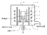
- This figure is the schematic of the manufacturing apparatus by the micro pulling-down method of the crystal
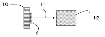
- This figure is a schematic diagram of a method for detecting ⁇ -ray excited luminescence of the scintillator for neutron beam detection according to the present invention.
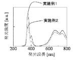
- This figure is an emission spectrum of the neutron beam detection scintillator of Examples 1 and 2 by ⁇ ray excitation.
- This figure is an emission spectrum of the neutron beam detection scintillators of Examples 3 and 4 by ⁇ ray excitation.
- This figure is the emission spectrum by the alpha ray excitation of the scintillator for neutron beam detection of Examples 5 and 6.
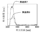
- This figure is an emission spectrum of the neutron beam detection scintillators of Examples 7 and 8 by ⁇ ray excitation.
- This figure is an emission spectrum of the neutron beam detection scintillators of Examples 9 and 10 by ⁇ ray excitation.
- This figure is an emission spectrum of the neutron beam detection scintillators of Examples 11 and 12 by ⁇ -ray excitation.
- This figure is an emission spectrum of the neutron beam detection scintillators of Examples 13 and 14 by ⁇ ray excitation.
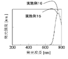
- This figure is the emission spectrum by the alpha ray excitation of the scintillator for neutron beam detection of Examples 15 and 16.
- This figure is an emission spectrum of the neutron beam detection scintillators of Examples 17 and 18 by ⁇ ray excitation.
- This figure is an emission spectrum of the neutron beam detection scintillator of Example 19 by ⁇ -ray excitation.
- This figure is an emission spectrum of the neutron beam detection scintillator of Example 20 by ⁇ ray excitation.
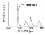
- This figure is an emission spectrum of the neutron beam detection scintillator of Example 21 by ⁇ ray excitation.
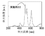
- This figure is an emission spectrum of the neutron beam detection scintillator of Example 22 by ⁇ ray excitation.
- This figure is an emission spectrum of the neutron beam detection scintillator of Example 23 by ⁇ ray excitation.
- This figure is an emission spectrum of the neutron beam detection scintillator of Example 24 by ⁇ -ray excitation.
- This figure is an emission spectrum of the neutron beam detection scintillator of Example 25 by ⁇ -ray excitation.
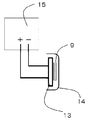
- This figure is a schematic diagram showing a neutron beam detection apparatus provided with a scintillator for neutron beam detection and a photodiode according to the present invention.
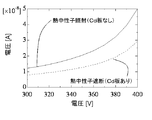
- This figure is a diagram showing current-voltage characteristics when light emitted when a thermal neutron beam is irradiated to the neutron beam detection scintillator of Example 16 is received by a silicon photodiode.
- This figure is a diagram showing current-voltage characteristics when the silicon neutron beam receives light emitted when the scintillator for detecting neutron beam of Example 18 is irradiated with a thermal neutron beam.
- This figure is a diagram showing current-voltage characteristics when the silicon neutron beam receives light emitted when a thermal neutron beam is irradiated to the neutron beam detection scintillator of Example 19.
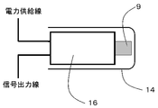
- This figure is a schematic view showing a neutron beam detection apparatus provided with a scintillator for neutron beam detection and a photomultiplier tube of the present invention.
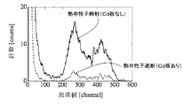
- This figure is a pulse height distribution spectrum diagram when a thermal neutron beam is irradiated to the neutron beam detector provided with the scintillator for neutron beam detection and the photomultiplier tube of Example 19.
- the neutron beam detection scintillator of the present invention is at least one fourth periodic element selected from the group consisting of Ti, V, Cr, Mn, Fe, Co, Ni, Cu and Zn (hereinafter referred to as “contained in the present invention”). 4), and a cordierite fluoride single crystal containing 6 Li of 0.80 atom / nm 3 or more.
- corkyrite means a naturally occurring LiCaAlF 6 compound and has a specific crystal structure.
- the corklite type is a compound having a structure similar to that of corkolite, and includes compounds in which elements in the compound are partially replaced with other elements.
- the cordierite-type fluoride single crystal is preferably a crystal having a basic structure of a single crystal of a compound represented by the chemical formula M X M Y M Z F 6 (hereinafter, M X M Y the single crystal of compound according to formula of M Z F 6 may be referred to as a Korukiraito type basic structure crystal).
- M X always including Li, Li, at least one element Na, K, is selected from the group consisting of Rb and Cs
- M Y is selected from the group consisting Ca, Mg, Ba, Sr, from Cd and Be at least one element
- M Z is, Al, represents at least one element selected from the group consisting of Ga and in.
- M X always include Li required to detect neutron radiation, preferably includes a Na When performing charge adjustment.
- M X , M Y and / or M Z in the compound represented by M X M Y M Z F 6 are , Partly replaced by a fourth periodic element.
- the single crystal is a hexagonal crystal belonging to the space group P31c, and can be easily identified by a powder X-ray diffraction technique.
- a single crystal represented by the chemical formula of LiCaAlF 6 , LiSrAlF 6 , LiCa 1-x Sr x AlF 6 (0 ⁇ x ⁇ 1) produced a large crystal. It is preferable in that it is easy and has high light emission intensity when used as a scintillator. In particular, LiCaAlF 6 is most preferable because it has a small effective atomic number, that is, low sensitivity to ⁇ rays.
- the cordierite-type fluoride single crystal used in the present invention includes at least one kind of fourth crystal selected from the group consisting of Ti, V, Cr, Mn, Fe, Co, Ni, Cu and Zn in the cordierite-type basic structure crystal.
- the fourth periodic element is contained in the crystal lattice of M X M Y M Z F 6 by substituting any element of M X , M Y , and M Z.
- the Mn element M Y, Cr element to replace the M Z.
- the content of the fourth periodic element is 0.01 mol% or more with respect to the single crystal compound having the basic structure, it is preferable because high emission intensity can be obtained at the time of neutron irradiation, and 0.1 mol% or more. If it exists, since higher luminescence intensity is obtained at the time of neutron irradiation, it is more preferable. Moreover, when there is too much content, the phenomenon that light emission intensity falls by the overlap of the light emission wavelength and absorption wavelength of this 4th period element becoming large, ie, concentration quenching, may occur. Therefore, the upper limit of the content is preferably 10 mol% or less, more preferably 5 mol% or less in the case of Ti, V, Fe, Co, Ni and Cu. In the case of Cr, Mn, and Zn, 50 mol% or less is preferable and 20 mol% or less is more preferable.
- the cordierite-type fluoride single crystal used in the present invention may contain at least one kind of rare earth element in addition to the fourth periodic element.
- the rare earth element is presumed to be present between the crystal lattices of the cordierite-type basic structure crystal or a part of the element constituting the crystal, but the exact form of existence is unknown.
- the rare earth elements are Ce, Eu, Pr, Nd, Er, Tm, Ho, Dy, Tb, Gd, Sm, Yb, La, Lu, Y, Sc, and Pm.
- a cordierite fluoride single crystal By including a rare earth element, it is possible to obtain a cordierite fluoride single crystal in which light emission in a specific wavelength region is increased or the light emission wavelength region is widened.
- a neutron detection scintillator made of a crystal with an extended emission wavelength region can be combined with a plurality of photodetectors having sensitivity to light in different wavelength regions. Specifically, when elements other than Ce and Eu are contained, light emission having a plurality of peak wavelengths can be obtained.
- a cordierite type fluorine light having an increased light emission in a wavelength region of 350 nm or more, which is mainly sensitive to silicon photodiodes. Compound single crystals can be obtained.
- the cordierite-type fluoride single crystal when a rare-earth element other than Ce and Eu is included in the cordierite-type fluoride single crystal, the sensitivity when combined with a silicon photodiode is improved as compared with the case where it is not included.
- Ce and Eu when Ce and Eu are contained, a cordierite-type fluoride single crystal having emission of a wavelength of 290 to 370 nm included in a wavelength region where the photomultiplier tube is sensitive can be obtained. Therefore, the cordierite fluoride single crystal containing Ce and Eu in addition to the fourth periodic element can be combined with not only a silicon photodiode but also a photomultiplier tube.
- Silicon photodiode and photomultiplier tube are photodetectors having different characteristics.
- a silicon photodiode is smaller and lighter than a photomultiplier tube, but has a difference in that the amplification factor is low and the response speed is slow.
- silicon photodiodes are strong against magnetic fields but weak against vibrations.
- photomultiplier tubes are weak against magnetic fields but strong against vibrations. Therefore, silicon photodiodes and photomultiplier tubes can be used for different purposes.
- a silicon photodiode is suitable as a medical radiation detector used in the vicinity of an MRI (nuclear magnetic resonance imaging) apparatus that generates a strong magnetic field, and as a radiation detector mounted on an excavator for logging in resource exploration.
- MRI magnetic resonance imaging
- a photomultiplier tube is suitable. Since these photodetectors have different wavelength ranges with high light receiving sensitivity, neutron beam scintillators that can be suitably used for both are limited in the scenes that can be used, for example, those having deliquescence. Other than that, little is known. However, such a material has high versatility and is very useful industrially.
- the rare earth element content is preferably 0.005 mol% or more because high emission intensity is easily obtained upon irradiation with neutron radiation, and more preferably 0.02 mol% or more because higher emission intensity is easily obtained. Moreover, since there exists a tendency for the growth of a single crystal to become difficult when there is too much content of rare earth elements, it is preferable that content is 5 mol% or less.
- the 6 Li content of the cordierite-type fluoride single crystal used in the present invention is preferably 0.80 atom / nm 3 or more. This is because the sensitivity to neutron beams necessary for use as a scintillator for detecting neutron beams is obtained. Furthermore, in order to increase the sensitivity to neutron rays, it is particularly preferable to the 6 Li content 4atom / nm 3 or more.
- the upper limit of the 6 Li content is 9 atoms / nm 3 .
- the 6 Li content that can be contained in the cordierite-type fluoride single crystal is theoretically about 9 atom / nm 3 at the maximum, and a 6 Li content higher than this cannot be obtained.
- the 6 Li content means the number of 6 Li elements contained per 1 nm 3 of the scintillator.
- the incident neutron beam causes a nuclear reaction with the 6 Li to generate ⁇ rays. Therefore, the 6 Li content affects the sensitivity to neutron beams, and the sensitivity to neutron beams increases as the 6 Li content increases.
- Such 6 Li content select a suitable for the composition of the crystalline compound which is a basic structure of the scintillator, or, it can be appropriately adjusted by adjusting the content ratio of 6 Li of LiF or the like used as the Li raw material.
- the existence ratio of 6 Li a presence ratio of 6 Li for all Li, existence ratio of natural is about 7.6%.
- a method for adjusting the abundance ratio of 6 Li a general-purpose raw material having 6 Li in a natural abundance ratio is used as a starting material, and the concentration is adjusted to the desired 6 Li abundance ratio, or the intended 6 There is a method in which a concentrated raw material concentrated to a ratio higher than the Li existing ratio is prepared, and the concentrated raw material and the general-purpose raw material are mixed and adjusted.
- the scintillator for detecting a neutron beam of the present invention is made of a single crystal, it does not cause loss due to non-radiative transition caused by lattice defects or scintillation light dissipation at the crystal grain boundary, and has high emission intensity.
- the cordierite-type fluoride single crystal used in the present invention is a transparent crystal that is colorless or slightly colored and has excellent scintillation light transmission. In addition, it has good chemical stability, and under normal conditions of use, no performance degradation is observed in a short period of time. Furthermore, mechanical strength and workability are also good, and it is easy to process and use it in a desired shape.
- the production method of the corklite-type fluoride single crystal used in the present invention is not particularly limited and can be produced by a known method, but is preferably produced by the Czochralski method or the micro pull-down method. This is because a cordierite-type fluoride single crystal excellent in quality such as transparency can be produced.
- the micro pull-down method the crystal can be directly manufactured into a specific shape and can be manufactured in a short time.
- the Czochralski method a large crystal having a diameter of several inches can be manufactured.
- the micro pulling-down method is a method for producing a crystal by drawing a raw material melt from a hole provided in the bottom of the crucible 5 using an apparatus as shown in FIG.
- a predetermined amount of raw material is filled into a crucible 5 having a hole at the bottom.
- the shape of the hole is not particularly limited, but is preferably a cylindrical shape having a diameter of 0.5 to 4 mm and a length of more than 0 mm and 2 mm or less.
- a cordierite type fluoride single crystal used in the present invention as raw materials, M X F, M Y F 2 , M Z F 3 , and a fluoride of the fourth periodic element contained in the present invention,
- a fluoride of the rare earth element When at least one kind of rare earth element is contained, it is preferable to use a fluoride of the rare earth element.
- the purity of these raw materials is not particularly limited, but each is preferably 99.99% or more.
- the mixed raw material may be used in the form of powder or granules, or may be used after being sintered or melted and solidified in advance.
- the LiF raw materials always contained in M X F, from the viewpoint of easily adjusting the 6 Li content of the scintillator, it is preferable to use a material obtained by concentrating a 6 Li.
- Concentration levels as long as 6 Li content of the scintillator is at a concentration such that 0.8atom / nm 3 or more, is not particularly limited, the more the content of 6 Li in the scintillator, neutrons were grown crystal since the neutron detection efficiency when used as a line for detecting scintillator higher, concentrated concentration such that the content is increased in 6 Li in the scintillator is preferred.
- the fluoride of the fourth periodic element and the fluoride of the rare earth element contained in the present invention can be blended so as to have a content in the above-mentioned range on the basis of M X M Y M Z F 6 .
- the weighed value of at least one fluoride raw material powder of M X , M Y , and M Z substituted by the additive element may be reduced by the blending amount.
- the blending amount of the fourth period element fluoride and the rare earth element fluoride used in the present invention may be set larger than the target content in consideration of the segregation phenomenon.
- the segregation coefficient used when calculating the content of the actual additive element from the blending amount varies depending on the growth conditions such as the type of additive element and the growth rate, so the actual concentration should be examined by elemental analysis for each crystal production condition. It is preferable to determine.
- the crucible 5 filled with the raw materials, the after heater 1, the heater 2, the heat insulating material 3, and the stage 4 are set as shown in FIG.
- an inert gas such as high purity argon is introduced into the chamber 6 to perform gas replacement.
- the pressure in the chamber after gas replacement is not particularly limited, but atmospheric pressure is common.
- the gas replacement operation can remove moisture adhering to the raw material or the chamber, and can prevent deterioration of crystals derived from such moisture.
- a solid scavenger such as zinc fluoride or a gas scavenger such as tetrafluoromethane.
- a method in which the scavenger is premixed in the raw material is suitable.
- a gas scavenger a method of mixing the scavenger with the inert gas and introducing it into the chamber is preferable.
- the raw material After performing the gas replacement operation, the raw material is heated and melted by the high-frequency coil 7, and the melted raw material melt is drawn out from the hole at the bottom of the crucible to start crystal growth.
- a metal wire is pulled down and provided at the tip of the rod.
- the metal wire is inserted into the crucible through the hole at the bottom of the crucible, and the raw material melt is attached to the metal wire. After the adhesion, the raw material melt is pulled down together with the metal wire, so that crystals can be grown.
- the metal wire is inserted into the hole at the bottom of the crucible and pulled out. This operation is repeated until the raw material melt is drawn together with the metal wire, and crystal growth is started.
- the material of the metal wire can be used without limitation as long as it is a material that does not substantially react with the raw material melt. However, a material excellent in corrosion resistance at high temperatures such as a W-Re alloy is preferable.
- the crystal After pulling out the raw material melt with the metal wire, the crystal can be obtained by continuously pulling it down at a constant pulling rate.
- the pulling speed is not particularly limited, but if it is too fast, the crystallinity tends to be poor, and if it is too slow, the crystallinity is improved, but the time required for crystal growth becomes enormous, so 0.5 to 10 mm. A range of / hr is preferred.
- an annealing operation may be performed after the production of the single crystal for the purpose of removing crystal defects caused by thermal strain.
- the obtained single crystal can be easily processed into a desired shape.
- a known cutting machine such as a blade saw or a wire saw, a grinding machine, or a polishing machine can be used without any limitation.
- the single crystal can be used as a scintillator by processing and polishing the single crystal into an appropriate shape for the photodetector.
- the shape of the scintillator for detecting a neutron beam according to the present invention is not particularly limited, but it is preferable that it has a light exit surface facing a photodetector described later, and the light exit surface is optically polished. By having such a light emitting surface, light generated by the scintillator can be efficiently incident on the photodetector.
- the shape of the light emitting surface is not limited, and a shape according to the application such as a quadrangle with a side length of several mm to several hundred mm square or a circle with a diameter of several mm to several hundred mm is appropriately selected. Can be used.
- the thickness of the scintillator with respect to the incident direction of the neutron beam varies depending on the energy of the neutron beam to be detected, but is generally several hundred ⁇ m to several hundred mm.
- a light reflecting film made of aluminum, Teflon (registered trademark) or the like is preferable to apply to the surface not facing the photodetector. This is to prevent the dissipation of light generated by the scintillator.
- the light emission of the scintillator for neutron beam detection according to the present invention can be detected by decomposing light into a spectrum using an arbitrary diffraction grating and CCD and measuring the spectrum.
- a CCD is a type of photodetector that includes a plurality of photodiodes. Any CCD can be used, but in consideration of the wavelength at which light can be received, the type of photodiode constituting the CCD is preferably a silicon photodiode.
- An electrical signal output from the CCD may be input to a personal computer via an arbitrary interface and analyzed. Such a spectroscopic detection method is preferable in that it easily separates an electric signal due to light emission of the scintillator and an electric signal due to noise.
- the neutron beam detection scintillator of the present invention can be combined with a photodetector to form a neutron beam detector.
- the presence and intensity of a neutron beam can be captured by converting light (scintillation light) emitted from a neutron beam detection scintillator by irradiation with a neutron beam into an electrical signal by a photodetector.
- the scintillation light emitted from the scintillator of the present invention varies depending on the additive element, the scintillation light includes light having a sensitivity of 350 nm or more with which the silicon photodiode has sensitivity.
- Examples of the photodetector include a photodiode and a photomultiplier tube.
- the wavelength dependence of the sensitivity of the photodetector varies depending on the type.
- a silicon photodiode is generally highly sensitive to light having a wavelength of 350 nm or more, particularly 400 nm or more.
- the scintillator for detecting a neutron beam of the present invention can be suitably used in combination with a photodiode, particularly a silicon photodiode, because it can emit light having a long wavelength of 350 nm or longer.
- the wavelength dependency of the sensitivity varies depending on the material of the photoelectric material and the photoelectric window. Therefore, it is necessary to select the type of photomultiplier tube to be used according to the emission wavelength of the scintillator.
- the photodiode can be suitably used for a small and lightweight neutron beam detector.
- an APD avalanche photodiode having an electric signal amplification function is preferably used in that the light of the scintillator can be received with high sensitivity.
- an avalanche photodiode S8664 series manufactured by Hamamatsu Photonics can be used.
- the neutron beam detection apparatus of the present invention can be obtained by bonding the scintillator for neutron beam detection of the present invention and the light receiving surface of the photodiode with an arbitrary optical grease such as silicon grease.
- the light-receiving surface of the photodiode to which the scintillator of the present invention is bonded may be covered with a light-shielding material of any material that is difficult to transmit light for the purpose of preventing the incidence of light in the environment.
- the surface other than the surface bonded to the photodiode may be covered with a reflecting material made of aluminum, Teflon (registered trademark), barium sulfate, or the like to increase the light collection efficiency.
- the detection device may have the function of both a material and a reflective material, and may cover the entire detection device.
- the detection device can be connected to an arbitrary current measuring device (for example, a picoammeter) to check the change in the current value, and the change in the current value according to the change in the amount of received light can be confirmed.
- a voltage may be applied to the silicon photodiode in a reverse bias, and in that case, any measuring instrument capable of simultaneously applying and measuring voltage or current (for example, KEITLEY 237, HIGH VOLTAGE SOURCE MEASURE UNIT may be used.
- the voltage value to be applied is preferably set according to the performance of the silicon photodiode and the flux of neutron to be measured.
- the scintillator and the light-receiving surface of the photomultiplier tube are bonded with an arbitrary optical grease or the like, as in the case of the photodiode.
- a neutron beam detector can be obtained.
- the light receiving surface of the photomultiplier tube to which the scintillator of the present invention is bonded may be covered with a light shielding material made of any material that is difficult to transmit light for the purpose of preventing the incidence of light in the environment.
- the scintillator of the present invention may be covered with a reflective material made of aluminum, Teflon (registered trademark), barium sulfate, or the like, except for the adhesive surface with the photomultiplier tube.
- the whole may be covered with the material function.
- the sensitivity of the photomultiplier tube is increased by applying a high voltage, and the detection of the neutron beam can be confirmed by observing the electric signal output from the photomultiplier tube.
- the electrical signal output from the photomultiplier tube may be input to an ammeter such as a picoammeter, the current-voltage characteristics may be evaluated, and the change in the amount of current may be confirmed to determine the intensity of the neutron beam. Further, the output electric signal may be input to an amplifier, a multi-wave height analyzer or the like and measured by photon counting (photon counting method).
- photon counting photon counting method
- a photodetector a silicon photodiode array or a position sensitive photomultiplier tube in which detectors having a sensitive area of several mm square are arranged in an array is used to cover part or all of the photocathode.
- a neutron beam imaging device by joining the scintillator of this invention.
- the scintillator may have an arbitrary shape, and can be a scintillator array in which plate-shaped, block-shaped, or quadrangular prism-shaped crystals are regularly arranged.
- the electrical signal output from the silicon photodiode array or the position sensitive photomultiplier tube can be read out using an arbitrary interface, and may be controlled by a personal computer using a control program.
- Example 1 Manufacture of neutron beam scintillators
- mold fluoride single crystal in Example 1 is demonstrated.
- Examples 2 to 25 were prepared in the same manner except that the type of element to be added and the raw material weighed value were different.
- a cordierite type fluoride single crystal used in the present invention was produced.
- the cordierite-type basic structure crystal was LiCaAlF 6 and Cu was used as the fourth periodic element.
- As the raw material purity of 99.99% or more LiF, a highly purified fluoride powder of CaF 2, AlF 3, CuF 2 .
- As the LiF 6 Li content ratio was used as 95%.
- the after heater 1, the heater 2, the heat insulating material 3, the stage 4, and the crucible 5 are made of high-purity carbon, and the shape of the hole provided at the bottom of the crucible is a circle having a diameter of 2.2 mm and a length of 0.5 mm. It was columnar.
- the crucible 5 was filled with the obtained mixed raw material.
- the crucible 5 filled with the raw material was set on the upper part of the after heater 1, and the heater 2 and the heat insulating material 3 were sequentially set around the crucible.
- the inside of the chamber 6 is evacuated to 5.0 ⁇ 10 ⁇ 4 Pa by using an evacuation apparatus composed of an oil rotary pump and an oil diffusion pump, and then a large amount of mixed gas of tetrafluoromethane and argon is introduced into the chamber 6. The gas was replaced by introducing the pressure up to atmospheric pressure.
- a high frequency current was applied to the high frequency coil 7, and the raw material was heated and melted by induction heating.
- a W-Re wire provided at the tip of the pull-down rod 8 was inserted into the hole at the bottom of the crucible 5, and the raw material melt was pulled down from the hole to start crystallization. While adjusting the output of the high frequency, it was continuously pulled down at a speed of 3 mm / hr for 17 hours to obtain a cordierite type fluoride single crystal used in the present invention.
- the crystal had a diameter of 2.1 mm and a length of 60 mm, and had good quality without white turbidity or cracks.
- the crystal is cut to a length of 10 mm by a wire saw equipped with a diamond wire, and then ground and mirror-polished, and processed into a shape having a length of 7 mm, a width of 2 mm, and a thickness of 1 mm. A scintillator was obtained.
- the 6 Li abundance ratio of the lithium raw material of the scintillator was 95%, and the density and molecular weight of LiCaAlF 6 were 3.0 g / cm 3 and 188 g / mol, respectively. Substituting these values into equation for calculating the 6 Li content above [1], 6 Li content was 8.3atom / nm 3. The amount of Cu added to the neutron beam scintillator was 0.5 mol% with respect to LiCaAlF 6 , and the calculated effective atomic number was about 15.
- Examples 2 to 25 For Examples 2 to 25, each material was weighed according to Table 1 below, and crystals were prepared, cut and polished in the same manner as in Example 1 except that the materials were added, and the neutron beam detection scintillator of the present invention was used. Obtained. In either embodiment, 6 Li content of the scintillator is 8.3atom / nm 3, the effective atomic number calculated was about 15.
- a 241 Am sealed radiation source 10 is installed in the vicinity of the neutron beam detection scintillator 9, irradiated with ⁇ rays, and the scintillation light 11 generated by excitation is incident on the CCD spectrometer 12.
- the 241 Am sealed radiation source 10 one having a radioactivity of 4 MBq was used.
- the CCD spectroscope 12 a spectroscope (KV-MV type spectroscope manufactured by Spectrometer Co., Ltd.) having a structure in which incident light is split by a diffraction grating and received by a CCD is used.
- the spectrometer was equipped with a newton manufactured by ANDOR TECHNOLOGY as a CCD, and a silicon photodiode was used for the CCD.
- 3 to 18 show the emission spectra of Examples 1 to 25 obtained.
- the horizontal axis indicates the emission wavelength, and the vertical axis indicates the emission intensity. Although each has a different emission wavelength, it contains light of 350 nm or more and was found to emit light with a light emission intensity detectable by the CCD.
- the scintillator of this invention light-emits when the alpha ray produced by the nuclear reaction of a thermal neutron beam and 6 Li excites a luminescent center element, and can be used as a scintillator for neutron beam detection.
- an avalanche photodiode (S8664-1010 manufactured by Hamamatsu Photonics) having sensitivity to light in a wavelength region of about 350 nm to 1000 nm was used.
- the neutron beam detection scintillator 9 of the present invention was adhered to the light receiving surface of the diode 13 with silicon grease and covered with a light shielding material 14 made of a black vinyl sheet to obtain the neutron beam detection apparatus of the present invention.
- the detection device was used in connection with an ammeter 15.
- the ammeter 15 is a KEITLEY 237 HIGH VOLTAGE SOURCE MEASURE UNIT that can read the current value while applying a voltage, and the current value while applying a voltage of 300 to 400 V with a reverse bias under the control of a program on a personal computer.
- the current-voltage characteristic graph was drawn.
- FIG. 20 shows a case where a neutron beam detector of the present invention comprising the scintillator of Example 16 is directly irradiated with a thermal neutron beam and a case where a shield plate is installed between the thermal neutron beam source and the detector. Shows current-voltage characteristics.
- a Cd (cadmium) 1 mm thick plate having high absorption efficiency for thermal neutron rays was used to reduce the flux of thermal neutrons irradiated to the scintillator.
- the current value at 350 V was 1.24 ⁇ 10 ⁇ 8 A when the thermal neutron beam was shielded, whereas it was 1.53 ⁇ 10 ⁇ 8 A when the thermal neutron beam was not shielded. It was found that the current value increased with increasing neutron flux.
- a neutron beam detector was prepared in the same manner as described above using the scintillators of Examples 18 and 19 instead of the scintillator of Example 16, and the current-voltage characteristics of the device were measured. The results are shown in FIGS. In both cases, the current value increased due to thermal neutron irradiation.
- thermal neutron radiation can be detected by combining the scintillator for detecting neutron radiation of the present invention and a silicon photodiode.
- FIG. 23 shows the configuration of the neutron beam detection apparatus of the present invention.
- the photomultiplier tube 16 R7600U manufactured by Hamamatsu Photonics Co., Ltd. having sensitivity to light of about 250 nm to 750 nm was used.
- the neutron beam detection scintillator 9 the scintillator of Example 19 was used. After the surface of the scintillator having a length of 7 mm and a width of 2 mm was adhered to the photocathode of the photomultiplier tube 16 with optical grease, the scintillator was shielded from light with a light shielding material 14 made of a black vinyl sheet so that light from the outside did not enter.
- the thermal neutron radiation source a 252 Cf sealed radiation source placed in a polyethylene container was used.
- scintillation light emitted from the scintillator was measured by a photon counting method.
- the scintillation light was converted into an electric signal through the photomultiplier tube 16 to which a high voltage of 600 V was applied.
- the electric signal output from the photomultiplier tube 16 is a pulse-like signal reflecting the scintillation light
- the pulse height represents the emission intensity of the scintillation light
- the waveform thereof is obtained when the scintillation light is attenuated.
- FIG. 24 shows pulse height distribution spectra when the neutron beam detector is directly irradiated with a thermal neutron beam and when a shield plate is installed between the thermal neutron beam source and the neutron beam detector.
- a Cd plate having a thickness of 1 mm was used in order to reduce the thermal neutron flux.
- the horizontal axis of the pulse height distribution spectrum represents the peak value of the electric signal, that is, the emission intensity of the scintillation light. Further, the vertical axis represents the frequency of the electric signal indicating each peak value, and here, it is indicated by the number of times (counts) the electric signal is measured.
- the neutron beam detection scintillator of the present invention has a sufficient light emission amount. From the above, it has been found that the neutron beam detection scintillator of the present invention operates as a neutron beam detector even when combined with a photomultiplier tube as well as a silicon photodiode.
Landscapes
- Chemical & Material Sciences (AREA)
- Spectroscopy & Molecular Physics (AREA)
- Inorganic Chemistry (AREA)
- General Physics & Mathematics (AREA)
- High Energy & Nuclear Physics (AREA)
- Molecular Biology (AREA)
- Physics & Mathematics (AREA)
- Health & Medical Sciences (AREA)
- Life Sciences & Earth Sciences (AREA)
- Engineering & Computer Science (AREA)
- Materials Engineering (AREA)
- Organic Chemistry (AREA)
- Measurement Of Radiation (AREA)
- Luminescent Compositions (AREA)
- Light Receiving Elements (AREA)
Abstract
本発明は、Ti、V、Cr、Mn、Fe、Co、Ni、Cu及びZnからなる群より選ばれる少なくとも一種類の第4周期元素を含有する、例えば、一般式MXMYMZF6(MXはLiを必ず含む、Li、Na等、MYはCaやMg等、MZはAlやGa等)で表されるようなコルキライト型フッ化物単結晶であって、6Liを0.80atom/nm3以上含有するコルキライト型フッ化物単結晶からなる中性子線検出用シンチレーター、及び該シンチレーターと光検出器とを備えた中性子線検出装置である。本発明の中性子線検出用シンチレーターは、シリコンフォトダイオードが高い感度を有する波長の蛍光を発し、且つ、有効原子番号が比較的小さくγ線によって発光を起こしにくい。
Description
本発明は、中性子線の検出に用いる中性子線検出用シンチレーターに関し、詳しくはTi、V、Cr、Mn、Fe、Co、Ni、Cu及びZnからなる群より選ばれる少なくとも一種類の第4周期元素を含有するコルキライト型フッ化物単結晶からなる中性子線検出用シンチレーター及び該シンチレーターを用いた中性子線検出装置に関する。
シンチレーターとは、α線、β線、γ線、X線、中性子線等の放射線が当たった時に当該放射線を吸収して蛍光を発する物質のことであり、光電子増倍管などの光検出器と組み合わせることで放射線検出に用いられる。そのため、シンチレーターは、断層撮影などの医療分野、非破壊検査などの工業分野、所持品検査などの保安分野、及び、高エネルギー物理学などの学術分野等、多くの分野で応用されている。
シンチレーターには、放射線の種類や使用目的に応じてさまざまな種類があり、例えば、ビスマスゲルマニウムオキサイド(Bi4Ge3O12)、セリウム添加ガドリニウムシリコンオキサイド(Ce:Gd2SiO5)などの無機結晶、アントラセンなどの有機結晶、有機蛍光体を含有させたポリスチレンやポリビニルトルエンなどの高分子体、または液体シンチレーターや気体シンチレーターがある。
従来、中性子線検出には、3Heと中性子線との3He(n,p)T反応を利用する3Heガスを用いた検出装置が主に用いられてきた。中性子線は、エネルギーに応じて、熱中性子線(約0.025eV)、熱外中性子線(約1eV)、低速中性子線(0.03~100eV)、中速中性子線(0.1~500keV)、高速中性子線(500keV以上)などに分類される。エネルギーの高い中性子線は、3He(n,p)T反応の発生確率が低く、即ち、3Heガスを用いた中性子線検出装置による検出感度が低い。従って、該中性子線検出装置の主な検出対象は、エネルギーの低い熱中性子線である。エネルギーの高い中性子線、例えば、高速中性子線を検出する場合は、ポリエチレンなどの減速材を用いて、高速中性子線を熱中性子線まで減速させてから検出する方法が用いられている。具体的には、3Heを用いた中性子線検出部を球形ポリエチレン減速材で覆ったレムカウンターやボナー球スペクトロメーターが使用されている。
上述のように、長らく、熱中性子線に対して感度の高い3Heガスを用いた中性子線検出装置が用いられてきた。しかし、3Heガスは希少であるため、近年、価格が高騰し、代替技術への置き換えが求められている。固体の中性子線検出用シンチレーターを用いた中性子線検出装置は、代替技術として有力な候補の一つである。
本発明において、中性子線が衝突すると蛍光を発する物質、及び該物質からなる成形体を、中性子線検出用シンチレーターと称する。
固体の中性子線検出用シンチレーターとして、リチウム6(6Li)を含有するシンチレーターは有望なものの一つである。該シンチレーターは、熱中性子線と6Liの核反応によりα線を生成し、次いで、該α線が発光中心元素を励起することにより発光する。α線による励起発光は、X線・γ線・β線とは機構が異なり、例えばシンチレーターの材料によってα線励起による発光量とX線励起による発光量の比であるα/β比が異なる等の違いが生じる。ゆえに、6Liを含有するシンチレーターの、中性子線検出用シンチレーターとしての性能を調べるには、α線を照射したときの発光を評価することが望ましく、中性子線を照射したときの発光を評価することがより望ましい。
固体の中性子線検出用シンチレーターの一例として、潮解性がなく、高速応答性を有するため、6Liガラスシンチレーターを挙げることができる。しかしながら、該シンチレーターは、製作工程が複雑であり、更に、ある程度以上の大きさに成形することができないという問題がある。
かかる問題に対して、本発明者らは、いくつかのフッ化物単結晶について、その中性子線検出用シンチレーターとしての応用を試みるべく、中性子線を照射して評価を行った。その結果、Liおよび2価以上の金属元素を含むフッ化物結晶に、ランタノイド及び単位体積当たり1.1~20原子(atom/nm3)の6Liを含有させ、さらに有効原子番号を10~40とすることで、中性子線検出用シンチレーターとして比較的良好な特性を有することを見出した(特許文献1参照)。
しかしながら、従来検討されてきた中性子線検出用シンチレーターは、主として、光検出器として光電子増倍管を用いる場合に好適なシンチレーターであった。即ち、該シンチレーターは、光電子増倍管によるフォトンカウンティング方式の中性子線検出装置に搭載するシンチレーターとしては十分に用いることができるが、サーベイメーターなどに好適に用いられる光検出器であるシリコンフォトダイオードと組み合わせて用いることについては、検討されていなかった。
シリコンフォトダイオードは長波長(概ね350nm以上、特に400nm以上)の光に対する感度は高いが、短波長の光に対する感度は低い。従って、短波長の光を受光する場合は十分な発光強度が必要となる。特許文献1に記載のセリウム添加リチウムカルシウムアルミニウムフルオライド(Ce:LiCaAlF6)はその発光波長領域が280~320nmであり、光検出器としてシリコンフォトダイオードを用いる場合に適さない。比較的長い発光波長を有する中性子線検出用シンチレーターの一例としては、発光波長540nmであるテルビウム添加ガドリニウムオキシサルファイド(Tb:Gd2O2S)が挙げられる。しかしながら、Tb:Gd2O2Sの有効原子番号は61であり、LiCaAlF6(有効原子番号14)やリチウムストロンチウムアルミニウムフルオライド〔LiSrAlF6(有効原子番号30)〕等と比べて非常に高く、即ち、γ線に対しても有感である。そのため、Tb:Gd2O2Sを用いる場合、中性子線だけを検出するのが困難であった。
また、シンチレーターの材料である単結晶の放射線励起発光は、様々な要因で消光(クエンチング)を起こす。そのため、実際にシンチレーターを作製して評価するまでは、単結晶からどのような発光が得られるかを予測するのは極めて困難であった。
本発明の目的は、シリコンフォトダイオードが高い感度を有する波長の蛍光を発し、且つ、有効原子番号が比較的小さくγ線による発光を起こしにくい中性子線検出用シンチレーターを提供することである。
本発明者等は、種々の組成でフッ化物単結晶を作製し、中性子線検出用シンチレーターとしての性能を評価するため、α線励起時の発光スペクトルをシリコンフォトダイオードからなるCCDにより測定した。その結果、Ti、V、Cr、Mn、Fe、Co、Ni、Cu及びZnからなる群より選ばれる少なくとも一種類の第4周期元素を含有するコルキライト型フッ化物単結晶からなる中性子線検出用シンチレーターにおいて、シリコンフォトダイオードで受光可能な発光が得られること、さらには、該シンチレーターとシリコンフォトダイオードとを組み合わせたものが中性子線検出器として動作できることを見出し、本発明を完成するに至った。
即ち、本発明により、Ti、V、Cr、Mn、Fe、Co、Ni、Cu及びZnからなる群より選ばれる少なくとも一種類の第4周期元素を含有し、更に6Liを0.80atom/nm3以上含有するコルキライト型フッ化物単結晶からなる中性子線検出用シンチレーターが提供される。
本発明の中性子線検出用シンチレーターにおいては、
1)希土類元素から選ばれる少なくとも一種の元素を更に含有すること、
2)該希土類元素がCe、Euから選ばれる少なくとも一種の元素であること、
3)前記コルキライト型フッ化物単結晶の基本構造が、下記の化学式;
MXMYMZF6
MXはLiを必ず含む、Li、Na、K、Rb及びCsからなる群よ
り選ばれる少なくとも一種類の元素である、
MYは、Ca、Mg、Ba、Sr、Cd及びBeからなる群より選ば
れる少なくとも一種類の元素である、
MZは、Al、Ga及びInからなる群より選ばれる少なくとも一種
類の元素である、
で表される化合物の単結晶体であること、
4)前記コルキライト型フッ化物単結晶の基本構造が、LiCaAlF6、LiSrAlF6及びLiCa1-xSrxAlF6(0<x<1)からなる群より選ばれるいずれかの化合物であること、
が好適である。
本発明により、また、前記中性子線検出用シンチレーター及び光検出器を備えることを特徴とする中性子線検出装置が提供される。
該中性子線検出装置の発明においては、光検出器がシリコンフォトダイオードであること、が好適である。
1)希土類元素から選ばれる少なくとも一種の元素を更に含有すること、
2)該希土類元素がCe、Euから選ばれる少なくとも一種の元素であること、
3)前記コルキライト型フッ化物単結晶の基本構造が、下記の化学式;
MXMYMZF6
MXはLiを必ず含む、Li、Na、K、Rb及びCsからなる群よ
り選ばれる少なくとも一種類の元素である、
MYは、Ca、Mg、Ba、Sr、Cd及びBeからなる群より選ば
れる少なくとも一種類の元素である、
MZは、Al、Ga及びInからなる群より選ばれる少なくとも一種
類の元素である、
で表される化合物の単結晶体であること、
4)前記コルキライト型フッ化物単結晶の基本構造が、LiCaAlF6、LiSrAlF6及びLiCa1-xSrxAlF6(0<x<1)からなる群より選ばれるいずれかの化合物であること、
が好適である。
本発明により、また、前記中性子線検出用シンチレーター及び光検出器を備えることを特徴とする中性子線検出装置が提供される。
該中性子線検出装置の発明においては、光検出器がシリコンフォトダイオードであること、が好適である。
本発明の中性子線検出用シンチレーターは、シリコンフォトダイオードで受光可能な蛍光を発する。シリコンフォトダイオードは小型且つ軽量である。従って、当該シンチレーターとシリコンフォトダイオードとを組み合わせたものは、環境中の中性子線の有無の判別などに用いることのできる、小型且つ軽量の中性子線検出装置として有用である。当該中性子線検出装置は、サーベイメーターなどの用途に好適である。
本発明の中性子線検出用シンチレーターは、Ti、V、Cr、Mn、Fe、Co、Ni、Cu及びZnからなる群より選ばれる少なくとも一種類の第4周期元素(以下、「本発明に含有される第4周期元素」と呼ぶことがある)を含有し、且つ、6Liを0.80atom/nm3以上含有するコルキライト型フッ化物単結晶からなる。尚、コルキライトとは、天然に存在するLiCaAlF6化合物を言い、特有の結晶構造を有する。また、コルキライト型とは、コルキライトに類似した構造を有する化合物であり、該化合物中の元素が他の元素に一部置き換わったものも含む。
本発明においてコルキライト型フッ化物単結晶として、好適には、MXMYMZF6の化学式で表される化合物の単結晶を基本構造とする結晶が例示される(以下、MXMYMZF6の化学式で表される化合物の単結晶をコルキライト型基本構造結晶と呼ぶことがある)。MXはLiを必ず含む、Li、Na、K、Rb及びCsからなる群より選ばれる少なくとも一種類の元素、MYは、Ca、Mg、Ba、Sr、Cd及びBeからなる群より選ばれる少なくとも一種類の元素、MZは、Al、Ga及びInからなる群より選ばれる少なくとも一種類の元素を表す。MXは中性子線を検出するのに必要なLiを必ず含み、電荷調整を行う場合はNaを含むことが好ましい。尚、後で詳細に説明するが、本発明に用いられるコルキライト型フッ化物単結晶においては、MXMYMZF6で表される化合物中のMX、MY及び/又はMZが、第4周期元素によって一部置換されている。
当該単結晶は、空間群P31cに属する六方晶であって、粉末X線回折の手法によって容易に同定することができる。
前記の化学式で表される化合物の単結晶の中でも、LiCaAlF6、LiSrAlF6、LiCa1-xSrxAlF6(0<x<1)の化学式で表わされる単結晶が、大型の結晶を作製しやすく、且つ、シンチレーターとして用いた際の発光強度が高いという点で、好ましい。特にLiCaAlF6は、有効原子番号が小さく、即ち、γ線に対する感度が小さいため、最も好ましい。
なお、本発明において、有効原子番号とは下記式;
有効原子番号=(ΣWiZi 4)1/4
式中、
Wiは、シンチレーターを構成する元素のうちのi番目の元素の質量
分率である、
Ziは、シンチレーターを構成する元素のうちのi番目の元素の原子
番号である、
で定義される指標である。
有効原子番号=(ΣWiZi 4)1/4
式中、
Wiは、シンチレーターを構成する元素のうちのi番目の元素の質量
分率である、
Ziは、シンチレーターを構成する元素のうちのi番目の元素の原子
番号である、
で定義される指標である。
本発明に用いるコルキライト型フッ化物単結晶は、前記コルキライト型基本構造結晶中に、Ti、V、Cr、Mn、Fe、Co、Ni、Cu及びZnからなる群より選ばれる少なくとも一種類の第4周期元素を含有する。該第4周期元素は、MX、MY、MZのいずれかの元素を置換してMXMYMZF6の結晶格子中に含有される。例えば、Mn元素はMYを、Cr元素はMZを置換する。該第4周期元素を含有することにより、中性子線照射時に、シリコンフォトダイオードが感度を有する350nm以上の波長域の光を含む発光が得られる。該第4周期元素の含有量は、基本構造となる単結晶化合物に対し、0.01モル%以上であれば、中性子線照射時に高い発光強度が得られるため好ましく、0.1モル%以上であれば、中性子線照射時により高い発光強度が得られるため、更に好ましい。また、含有量が多すぎる場合、該第4周期元素の発光波長と吸収波長の重なりが大きくなることで発光強度が低下してしまう現象、即ち濃度消光が起こることがある。そのため、含有量の上限はTi、V、Fe、Co、Ni、Cuの場合は10モル%以下が好ましく、5モル%以下がより好ましい。Cr、Mn、Znの場合、50モル%以下が好ましく、20モル%以下がより好ましい。
更に、本発明に用いるコルキライト型フッ化物単結晶は、該第4周期元素に加えて、少なくとも1種類の希土類元素を含んでいても良い。該希土類元素は、コルキライト型基本構造結晶の結晶格子間や結晶を構成する元素の一部と置換して存在するものと推測されるが、正確な存在形態は不明である。なお、本発明において、希土類元素とは、Ce、Eu、Pr、Nd、Er、Tm、Ho、Dy、Tb、Gd、Sm、Yb、La、Lu、Y、Sc、Pmである。
希土類元素を含有させることで、特定の波長域の発光が増加したり、発光波長領域が広がったコルキライト型フッ化物単結晶を得ることができる。発光波長領域が広がった結晶からなる中性子検出用シンチレーターは、異なる波長領域の光に感度を有する複数の光検出器と組み合わせることができる。
具体的には、Ce、Eu以外の元素を含有させると、複数のピーク波長を有する発光が得られるが、主にシリコンフォトダイオードが感度を有する350nm以上の波長域の発光が増加したコルキライト型フッ化物単結晶を得ることができる。即ち、コルキライト型フッ化物単結晶にCe、Eu以外の希土類元素を含有させると、含有させない場合に比べ、シリコンフォトダイオードと組み合わせた時の感度が良くなる。一方、Ce、Euを含有させると、光電子増倍管が感度を有する波長域に含まれる290~370nmの波長の発光を有するコルキライト型フッ化物単結晶を得ることができる。従って、該第4周期元素に加えてCe、Euを含有させたコルキライト型フッ化物単結晶は、シリコンフォトダイオードだけでなく光電子増倍管とも組み合わせることができる。
具体的には、Ce、Eu以外の元素を含有させると、複数のピーク波長を有する発光が得られるが、主にシリコンフォトダイオードが感度を有する350nm以上の波長域の発光が増加したコルキライト型フッ化物単結晶を得ることができる。即ち、コルキライト型フッ化物単結晶にCe、Eu以外の希土類元素を含有させると、含有させない場合に比べ、シリコンフォトダイオードと組み合わせた時の感度が良くなる。一方、Ce、Euを含有させると、光電子増倍管が感度を有する波長域に含まれる290~370nmの波長の発光を有するコルキライト型フッ化物単結晶を得ることができる。従って、該第4周期元素に加えてCe、Euを含有させたコルキライト型フッ化物単結晶は、シリコンフォトダイオードだけでなく光電子増倍管とも組み合わせることができる。
シリコンフォトダイオードと光電子増倍管は、異なる特徴を有する光検出器である。シリコンフォトダイオードは光電子増倍管に比べ、小型且つ軽量であるが、増幅率が低い、応答速度が遅いといった違いがある。また、シリコンフォトダイオードは磁場に強いが振動に弱く、逆に光電子増倍管は磁場に弱いが振動に強いといった特徴がある。そのため、シリコンフォトダイオードと光電子増倍管は使用できる用途が異なっている。例えば、強い磁場を発生するMRI(核磁気共鳴画像法)装置の周辺で用いる医療用放射線検出器としてはシリコンフォトダイオードが適し、資源探査における検層用の掘削機に搭載される放射線検出器としては、振動が大きいため、光電子増倍管が適する。これらの光検出器は受光感度の高い波長領域が異なっているため、両方に好適に用いることのできる中性子線検出用シンチレーターは、利用できる場面が限定されるもの、例えば潮解性を有するものなどを除いては、ほとんど知られていない。しかしながら、そのような材料は汎用性が高く工業的に非常に有用である。
希土類元素の含有量は、中性子線照射時に高い発光強度が得られやすいため、0.005モル%以上が好適であり、更に高い発光強度が得られやすいため、0.02モル%以上がより好ましい。また、希土類元素の含有量が多すぎる場合、単結晶の育成が困難になる傾向にあるため、含有量は5モル%以下とすることが好ましい。
本発明に用いるコルキライト型フッ化物単結晶の6Li含有量は0.80atom/nm3以上であることが好ましい。中性子線検出用シンチレーターとして用いるのに必要な、中性子線に対する感度が得られるからである。さらに、中性子線に対する感度をより高めるためには、該6Li含有量を4atom/nm3以上とすることが特に好ましい。
6Li含有量の上限は9atom/nm3である。コルキライト型フッ化物単結晶に含有させることのできる6Li含有量は、理論上最大で9atom/nm3程度であり、これ以上の6Li含有量のものを得ることはできない。
本発明において、上記6Li含有量とはシンチレーター1nm3あたりに含まれる6Li元素の個数をいう。入射した中性子線は、この6Liと核反応を起こしてα線を生じる。従って、該6Li含有量は中性子線に対する感度に影響し、6Li含有量が多いほど中性子線に対する感度が向上する。
かかる6Li含有量は、シンチレーターの基本構造となる結晶化合物の組成について好適なものを選択するか、または、Li原料として用いるLiF等の6Liの存在比率を調整することによって適宜調整できる。ここで、6Liの存在比率とは、全Liに対する6Liの存在比率であり、天然の存在比率は約7.6%である。6Liの存在比率を調整する方法としては、天然の存在比率で6Liを有する汎用原料を出発原料として、所期の6Li存在比率まで濃縮して調整する方法、或いは、あらかじめ所期の6Li存在比率以上に濃縮された濃縮原料を用意し、該濃縮原料と前記汎用原料を混合して調整する方法が挙げられる。
なお、上記6Li含有量(atom/nm3)は、下式〔1〕;
6Li含有量=A×C×ρ×10-23/M 〔1〕
式中、
Aはアボガドロ数[6.02×10²³]を示す、
CはLi原料における、全Liに対する6Liの存在比率[%]、
ρは本発明のシンチレーターに用いるコルキライト型フッ化物単結晶
の密度[g/cm3]、
Mは本発明のシンチレーターに用いるコルキライト型フッ化物単結晶
の分子量[g/mol]、
によって求めることができる。
6Li含有量=A×C×ρ×10-23/M 〔1〕
式中、
Aはアボガドロ数[6.02×10²³]を示す、
CはLi原料における、全Liに対する6Liの存在比率[%]、
ρは本発明のシンチレーターに用いるコルキライト型フッ化物単結晶
の密度[g/cm3]、
Mは本発明のシンチレーターに用いるコルキライト型フッ化物単結晶
の分子量[g/mol]、
によって求めることができる。
本発明の中性子線検出用シンチレーターは単結晶からなっているので、格子欠陥に起因する非輻射遷移や結晶粒界でのシンチレーション光の散逸などによるロスを生じることがなく、発光強度が高い。
本発明に用いるコルキライト型フッ化物単結晶は、無色ないしはわずかに着色した透明な結晶であり、シンチレーション光の透過性に優れる。また、良好な化学的安定性を有しており、通常の使用状況下では、短期間での性能の劣化は認められない。更に、機械的強度及び加工性も良好であり、所望の形状に加工して用いることが容易である。
本発明に用いるコルキライト型フッ化物単結晶の製造方法は特に限定されず、公知の方法によって製造することができるが、チョクラルスキー法、またはマイクロ引き下げ法によって製造することが好ましい。透明性等の品質に優れたコルキライト型フッ化物単結晶を製造することができるからである。マイクロ引き下げ法によれば、結晶を特定の形状に直接製造することができ、しかも短時間で製造することができる。一方、チョクラルスキー法によれば、直径が数インチの大型結晶を製造することが可能となる。
マイクロ引き下げ法とは、図1に示すような装置を用いて、坩堝5の底部に設けた孔より原料融液を引き出して結晶を製造する方法である。
以下、マイクロ引き下げ法によって本発明に用いるフッ化物単結晶を製造する際の、一般的な方法について説明する。
まず、所定量の原料を、底部に孔を設けた坩堝5に充填する。孔の形状は、特に限定されないが、直径が0.5~4mm、長さが0mmより大きく2mm以下の円柱状とすることが好ましい。
本発明に用いるコルキライト型フッ化物単結晶を製造するにあたり、原料として、MXF、MYF2、MZF3、及び、本発明に含有される第4周期元素のフッ化物、更に、少なくとも1種類の希土類元素を含有させる場合には、該希土類元素のフッ化物を用いることが好ましい。これらの原料の純度は特に限定されないが、それぞれ99.99%以上であることが好ましい。更に、製造の際には、これらのフッ化物を混合した、混合原料を用いることが好ましい。かかる混合原料を用いることにより、結晶の純度を高めることができ、発光強度等の特性が向上する。混合原料は、粉末状あるいは粒状で用いても良く、あらかじめ焼結或いは溶融固化させてから用いてもよい。
また、MXFに必ず含有するLiFの原料には、シンチレーターの6Li含有量を調整しやすいという観点から、6Liを濃縮したものを用いることが好ましい。濃縮濃度は、シンチレーターの6Li含有量が0.8atom/nm3以上となるような濃度である限り、特に制限はないが、シンチレーター中の6Liの含有量が多いほど、育成した結晶を中性子線検出用シンチレーターとして用いる際の中性子線検出効率が高くなるため、シンチレーター中の6Liの含有量が多くなるような濃縮濃度が、好ましい。
上記混合原料のうちMXF、MYF2、MZF3は、MX:MY:MZ=1:1:1(モル比)の比率となるように秤量し、混合すればよい。本発明に含有される第4周期元素のフッ化物及び希土類元素のフッ化物は、MXMYMZF6を基準にして、前記した範囲の含有量となるように配合できる。その際、添加元素が置換するMX、MY、MZの少なくとも一種類のフッ化物原料粉末の秤量値を配合量の分、減らしても良い。
本発明に用いられる第4周期元素のフッ化物及び希土類元素のフッ化物の配合量は、偏析現象を考慮し、目標とする含有量よりも多めに設定しても良い。配合量から実際の添加元素の含有量を算出する際に用いる偏析係数は、添加元素の種類や成長速度など育成条件によって変動するため、結晶作製条件ごとに元素分析などで実際の濃度を調べて決定することが好ましい。
また、高温で揮発性が高い原料は、多めに配合しても良い。揮発量は、結晶育成条件(温度・雰囲気・工程)によって全く異なる。従って、予め揮発量を調べ、該揮発量を考慮して配合量を決めることが望ましい。
次いで、上記原料を充填した坩堝5、アフターヒーター1、ヒーター2、断熱材3、及びステージ4を図1に示すようにセットする。真空排気装置を用いて、チャンバー6内を1.0×10⁻³Pa以下まで真空排気した後、高純度アルゴン等の不活性ガスをチャンバー6内に導入してガス置換を行う。ガス置換後のチャンバー内の圧力は特に限定されないが、大気圧が一般的である。
該ガス置換操作によって、原料或いはチャンバー内に付着した水分を除去することができ、かかる水分に由来する結晶の劣化を妨げることができる。上記ガス置換操作によっても除去できない水分による影響を避けるため、フッ化亜鉛等の固体スカベンジャー或いは四フッ化メタン等の気体スカベンジャーを用いることが好ましい。固体スカベンジャーを用いる場合には、該スカベンジャーを原料中に予め混合しておく方法が好適である。気体スカベンジャーを用いる場合には、該スカベンジャーを上記不活性ガスに混合してチャンバー内に導入する方法が好適である。
ガス置換操作を行った後、高周波コイル7で原料を加熱して溶融させ、溶融した原料融液を坩堝底部の孔から引き出して、結晶の育成を開始する。
ここで、金属ワイヤーを引き下げロッドの先端に設ける。該金属ワイヤーを坩堝底部の孔から坩堝内部に挿入し、該金属ワイヤーに原料融液を付着させる。付着後、原料融液を金属ワイヤーと共に引き下げることによって結晶の育成が可能となる。
即ち、高周波の出力を調整し、原料の温度を徐々に上げながら、該金属ワイヤーを坩堝底部の孔に挿入し、引き出しを行う。この操作を、原料融液が金属ワイヤーと共に引き出されるまで繰り返して、結晶の育成を開始する。該金属ワイヤーの材質は、原料融液と実質的に反応しない材質であれば制限無く使用できるが、W-Re合金等の高温における耐食性に優れた材質が好適である。
上記金属ワイヤーによる原料融液の引き出しを行った後、一定の引き下げ速度で連続的に引き下げることにより、結晶を得ることができる。
該引き下げ速度は、特に限定されないが、速過ぎると結晶性が悪くなりやすく、遅過ぎると、結晶性は良くなるものの、結晶育成に必要な時間が膨大になってしまうため、0.5~10mm/hrの範囲が好ましい。
本発明に用いるコルキライト型フッ化物単結晶の製造において、熱歪に起因する結晶欠陥を除去する目的で、単結晶の製造後にアニール操作を行っても良い。
得られた単結晶は、所望の形状に容易に加工できる。加工に際しては、公知のブレードソー、ワイヤーソー等の切断機、研削機、或いは研磨盤を何ら制限無く用いることができる。該単結晶を、光検出器に対して適切な形状に加工研磨することでシンチレーターとして使用することができる。
本発明の中性子線検出用シンチレーターの形状は特に制限されないが、後述する光検出器に対向する光出射面を有し、当該光出射面は光学研磨が施されていることが好ましい。かかる光出射面を有することによって、シンチレーターで生じた光を効率よく光検出器に入射できる。
なお、前記光出射面の形状は限定されず、一辺の長さが数mm~数百mm角の四角形、或いは直径が数mm~数百mmの円など、用途に応じた形状を適宜選択して用いることができる。
シンチレーターの中性子線入射方向に対する厚さは、検出対象とする中性子線のエネルギーによって異なるが、一般に数百μm~数百mmである。
光検出器に対向しない面に、アルミニウム或いはテフロン(登録商標)等からなる光反射膜を施すことが好ましい。シンチレーターで生じた光の散逸を防止するためである。
本発明の中性子線検出用シンチレーターの発光は、任意の回折格子及びCCDを用いて、光をスペクトルに分解し、該スペクトルを測定することにより、検出することができる。CCDとは複数のフォトダイオードで構成される光検出器の一種である。CCDには任意のものを使用できるが、受光可能な波長を考慮すると、CCDを構成するフォトダイオードの種類がシリコンフォトダイオードであることが好ましい。CCDから出力される電気信号を任意のインターフェイスを介してパーソナルコンピューターに入力し、解析しても良い。このような分光による検出方法は、シンチレーターの発光による電気信号とノイズによる電気信号とを分離しやすい点で、好ましい。
本発明の中性子線検出用シンチレーターは、光検出器と組み合わせて中性子線検出装置とすることができる。
即ち、中性子線の照射により中性子線検出用シンチレーターから発せられた光(シンチレーション光)を、光検出器によって電気信号に変換することによって、中性子線の有無及び強度を捉えることができる。本発明のシンチレーターから発せられるシンチレーション光は、添加元素によって異なるが、シリコンフォトダイオードが感度を有する350nm以上の光を含んでいる。
光検出器としては、フォトダイオード、光電子増倍管などが挙げられる。光検出器の感度の波長依存性は種類によって異なり、例えばシリコンフォトダイオードは一般に、350nm以上、特に400nm以上の波長の光に対して感度が高い。本発明の中性子線検出用シンチレーターは、350nm以上の長波長の発光が得られるためフォトダイオード、特にシリコンフォトダイオードと組み合わせて好適に使用できる。光電子増倍管の場合、光電材料や光電窓の材質の違いによっても感度の波長依存性が異なるため、シンチレーターの発光波長に応じて、使用する光電子増倍管の種類を選択する必要がある。
フォトダイオードは、小型且つ軽量な中性子線検出装置に好適に使用できる。フォトダイオードは任意のものを用いることができるが、高感度にシンチレーターの光を受光できるという点で、電気信号の増幅機能を有するAPD(アバランシェフォトダイオード)が好適に使用される。一例を挙げると浜松ホトニクス社製アバランシェフォトダイオードS8664シリーズを用いることができる。
本発明の中性子線検出用シンチレーターと該フォトダイオードの受光面とをシリコングリースなどの任意の光学グリースで接着することで、本発明の中性子線検出装置を得ることができる。本発明のシンチレーターを接着したフォトダイオードの受光面は、環境中の光の入射を防ぐ目的で、光を通しにくい任意の材質の遮光材で覆っても良い。本発明のシンチレーターのうち、フォトダイオードと接着している面以外の面を、アルミニウム、テフロン(登録商標)、硫酸バリウムなどからなる反射材で覆って集光効率を高めても良く、前記した遮光材と反射材の機能を併せ持つもので該検出装置の全体を覆っても良い。該検出装置を任意の電流測定器(例えばピコアンメーター)に接続して電流値の変化を調べ、受光量の変化に応じた電流値の変化を確認することができる。その際に、受光感度を向上させる目的で、シリコンフォトダイオードには逆バイアスに電圧を印加してもよく、その場合、電圧または電流の印加と測定を同時に行うことのできる任意の計測器(例えば、KEITHLEY 237 HIGH VOLTAGE SOURCE MEASURE UNIT)を用いてもよい。印加する電圧値は、シリコンフォトダイオードの性能や測定する中性子のフラックスに応じて設定することが好ましい。例えば、浜松ホトニクス社製アバランシェフォトダイオードS8664シリーズを使用する場合は300~400Vの電圧の印加が特に好ましい。設定した動作電圧において、事前に照射された熱中性子のフラックスと電流値の関係を測定しておくことで、定量性を有する中性子線検出装置として用いることもできる。
本発明の中性子線検出用シンチレーターにCe、Euを含有させた場合は、フォトダイオードの場合と同様にして、該シンチレーターと光電子増倍管の受光面とを任意の光学グリース等で接着して、中性子線検出装置を得ることができる。本発明のシンチレーターを接着した光電子増倍管の受光面は、環境中の光の入射を防ぐ目的で、光を通しにくい任意の材質の遮光材で覆っても良い。本発明のシンチレーターの、光電子増倍管との接着面以外を、アルミニウム、テフロン(登録商標)、硫酸バリウムなどからなる反射材で覆って集光効率を高めても良く、前記した遮光材と反射材の機能を併せ持つもので全体を覆っても良い。光電子増倍管は、高電圧を印加することでその感度を高め、該光電子増倍管から出力される電気信号を観測することで、中性子線の検出を確認できる。
光電子増倍管から出力される電気信号を、ピコアンメーターなどの電流計に入力し、電流電圧特性を評価し、電流量の変化を確認することで中性子線の強度を判別してもよい。また、出力される電気信号を、増幅器や多重波高分析器等に入力し、フォトンカウンティング(光子計数法)によって測定してもよい。ただし、シンチレーターの蛍光寿命が長い場合等は、フォトンカウンティングでは測定が難しいこともある。本発明の中性子線検出用シンチレーターの内、Ce、Euを含有するものは、フォトンカウンティングによる測定に対しても好適に使用できる。
更に、光検出器として、数mm角の有感領域を有する検出部をアレイ状に配列してなるシリコンフォトダイオードアレイもしくは位置敏感型光電子増倍管を用い、光電面の一部または全部を覆うように本発明のシンチレーターを接合することで、中性子線撮像装置とすることができる。
シリコンフォトダイオードアレイもしくは位置敏感型光電子増倍管としては、本発明のシンチレーターから発せられるシンチレーション光を検出することができるものを用いる。光検出器の受光面と本発明のシンチレーターとの接合には光学グリース等を用いてもよい。シンチレーターは任意の形状で良く、板状、ブロック状、もしくは四角柱形状の結晶を規則的に配列させたシンチレーターアレイとすることができる。
シリコンフォトダイオードアレイもしくは位置敏感型光電子増倍管から出力される電気信号は、任意のインターフェイスを用いて読み出すことができ、パーソナルコンピューターで制御用プログラムを用いて制御してもよい。
以下、本発明の実施例を挙げて具体的に説明するが、本発明はこれらの実施例によって何ら制限されるものではない。また、実施例中で説明されている特徴の組み合わせすべてが本発明の解決手段に必須のものとは限らない。
(中性子線検出用シンチレーターの製造)
以下、実施例1におけるコルキライト型フッ化物単結晶の製造方法を説明する。表1に示すように、添加する元素の種類及び原料秤量値が異なることを除いて、実施例2~25においても同様の方法で作製した。
以下、実施例1におけるコルキライト型フッ化物単結晶の製造方法を説明する。表1に示すように、添加する元素の種類及び原料秤量値が異なることを除いて、実施例2~25においても同様の方法で作製した。
<実施例1>
図1に示すマイクロ引き下げ法による結晶製造装置を用いて、本発明に用いるコルキライト型フッ化物単結晶を製造した。コルキライト型基本構造結晶をLiCaAlF6とし、第4周期元素としてCuを用いた。原料としては、純度が99.99%以上のLiF、CaF2、AlF3、CuF2の高純度フッ化物粉末を用いた。なお、LiFとしては、6Li存在比率が95%のものを用いた。アフターヒーター1、ヒーター2、断熱材3、ステージ4、及び坩堝5は、高純度カーボン製のものを使用し、坩堝底部に設けた孔の形状は直径2.2mm、長さ0.5mmの円柱状とした。
図1に示すマイクロ引き下げ法による結晶製造装置を用いて、本発明に用いるコルキライト型フッ化物単結晶を製造した。コルキライト型基本構造結晶をLiCaAlF6とし、第4周期元素としてCuを用いた。原料としては、純度が99.99%以上のLiF、CaF2、AlF3、CuF2の高純度フッ化物粉末を用いた。なお、LiFとしては、6Li存在比率が95%のものを用いた。アフターヒーター1、ヒーター2、断熱材3、ステージ4、及び坩堝5は、高純度カーボン製のものを使用し、坩堝底部に設けた孔の形状は直径2.2mm、長さ0.5mmの円柱状とした。
まず、表1に示す通りに原料をそれぞれ秤量し、よく混合して混合原料を得た。得られた混合原料を坩堝5に充填した。原料を充填した坩堝5を、アフターヒーター1の上部にセットし、その周囲にヒーター2、及び断熱材3を順次セットした。次いで、油回転ポンプ及び油拡散ポンプからなる真空排気装置を用いて、チャンバー6内を5.0×10⁻⁴Paまで真空排気した後、四フッ化メタン-アルゴン混合ガスをチャンバー6内に大気圧まで導入し、ガス置換を行った。
高周波コイル7に高周波電流を印加し、誘導加熱によって原料を加熱して溶融させた。引き下げロッド8の先端に設けたW-Reワイヤーを、坩堝5底部の上記孔に挿入し、原料の融液を上記孔より引き下げ、結晶化を開始した。高周波の出力を調整しながら、3mm/hrの速度で連続的に17時間引き下げ、本発明に用いるコルキライト型フッ化物単結晶を得た。
該結晶は直径が2.1mm、長さが60mmであり、白濁やクラックの無い良質なものであった。
該結晶を、ダイヤモンドワイヤーを備えたワイヤーソーによって10mmの長さに切断した後、研削及び鏡面研磨を行い、長さ7mm、幅2mm、厚さ1mmの形状に加工し、本発明の中性子線検出用シンチレーターを得た。
該シンチレーターのリチウム原料の6Li存在比率は95%であり、LiCaAlF6の密度、分子量が、それぞれ3.0g/cm3、188g/molであった。これらの値を上記した6Li含有量の算出式〔1〕に代入すると、6Li含有量は8.3atom/nm3であった。また、該中性子線検出用シンチレーターのCuの添加量はLiCaAlF6に対し0.5モル%で、算出される有効原子番号は約15であった。
<実施例2~25>
実施例2~25についても、下記の表1に従って各材料を秤量し、添加した点以外は、実施例1と同様にして結晶を作製、切断、研磨し、本発明の中性子線検出用シンチレーターを得た。何れの実施例においても、該シンチレーターの6Li含有量は8.3atom/nm3で、算出される有効原子番号は約15であった。
実施例2~25についても、下記の表1に従って各材料を秤量し、添加した点以外は、実施例1と同様にして結晶を作製、切断、研磨し、本発明の中性子線検出用シンチレーターを得た。何れの実施例においても、該シンチレーターの6Li含有量は8.3atom/nm3で、算出される有効原子番号は約15であった。


(α線励起発光の検出)
実施例1~25の中性子線検出用シンチレーターのα線励起発光を下記の方法によって検出した。
実施例1~25の中性子線検出用シンチレーターのα線励起発光を下記の方法によって検出した。
図2に示す模式図のように、中性子線検出用シンチレーター9の近傍に241Am密封線源10を設置してα線を照射し、励起されて生じたシンチレーション光11をCCD分光器12に入射して200nm~800nmの発光スペクトルを取得した。241Am密封線源10としては4MBqの放射能を有するものを用いた。CCD分光器12としては、入射光を回折格子で分光してCCDで受光する構造の分光器(分光計器社製のKV-MV型分光器)を使用した。該分光器は、CCDとしてANDOR TECHNOLOGY社製のnewtonを搭載しており、該CCDにはシリコンフォトダイオードが用いられていた。
図3~18に、得られた実施例1~25の発光スペクトルを示す。横軸が発光波長、縦軸が発光強度を示している。それぞれ、発光波長は異なるものの、350nm以上の光を含んでおり、CCDで検出可能な発光強度で発光していることがわかった。これにより、本発明のシンチレーターが、熱中性子線と6Liの核反応により生じるα線が発光中心元素を励起することによって発光し、中性子線検出用シンチレーターとして使用できることがわかった。
(シリコンフォトダイオードを備えた中性子線検出装置の作製)
実施例16のシンチレーターを、図19に示すように、シリコンフォトダイオード13と組み合わせることによって、中性子線検出装置を作成した。得られた検出装置について、熱中性子線を照射したときの電流電圧特性を調べた。
実施例16のシンチレーターを、図19に示すように、シリコンフォトダイオード13と組み合わせることによって、中性子線検出装置を作成した。得られた検出装置について、熱中性子線を照射したときの電流電圧特性を調べた。
シリコンフォトダイオード13としては、約350nm~1000nmの波長領域の光に感度を有するアバランシェフォトダイオード(浜松ホトニクス社製S8664-1010)を使用した。該ダイオード13の受光面に本発明の中性子線検出用シンチレーター9を、シリコングリースを用いて接着し、黒色のビニールシートからなる遮光材14で覆い、本発明の中性子線検出装置とした。該検出装置は、電流計15と接続して用いた。電流計15として、電圧を印加しながら電流値を読み取ることのできるKEITHLEY 237 HIGH VOLTAGE SOURCE MEASURE UNITを用い、パーソナルコンピューター上のプログラムによる制御によって、逆バイアスで300~400Vの電圧を印加しながら電流値の計測を行い、電流電圧特性のグラフを描画した。
熱中性子線源としては、252Cf密封線源をポリエチレン容器に入れたものを用いた。図20に、実施例16のシンチレーターからなる本発明の中性子線検出装置に熱中性子線を直接照射した場合と、熱中性子線源と該検出装置の間に遮蔽板を設置して照射した場合の、電流電圧特性を示す。遮蔽板としては、シンチレーターに照射される熱中性子のフラックスを低減させるため、熱中性子線に対して高い吸収効率を持つCd(カドミウム)の厚み1mmの板を用いた。350Vにおける電流値は、熱中性子線を遮蔽した場合は1.24×10⁻⁸Aだったのに対し、熱中性子線を遮蔽しなかった場合は1.53×10⁻⁸Aであり、熱中性子のフラックスの増加に伴って電流値が増加することがわかった。
実施例16のシンチレーターの代わりに、実施例18及び19のシンチレーターを用いて、上記と同様にして、中性子線検出装置を作成し、該装置の電流電圧特性を測定した。その結果をそれぞれ図21、22に示す。どちらの場合も、熱中性子線の照射により電流値が増加した。
以上により、本発明の中性子線検出用シンチレーターとシリコンフォトダイオードを組み合わせることで、熱中性子線の検出が可能であることが確認された。
(光電子増倍管を備えた中性子線検出装置の作製)
図23に本発明の中性子線検出装置の構成を示す。光電子増倍管16としては、約250nm~750nmの光に感度を有する浜松ホトニクス社製R7600Uを用いた。中性子線検出用シンチレーター9としては、実施例19のシンチレーターを用いた。該シンチレーターの長さ7mm、幅2mmの面を光電子増倍管16の光電面に光学グリースで接着した後、外部からの光が入らないように黒色のビニールシートからなる遮光材14で遮光した。
図23に本発明の中性子線検出装置の構成を示す。光電子増倍管16としては、約250nm~750nmの光に感度を有する浜松ホトニクス社製R7600Uを用いた。中性子線検出用シンチレーター9としては、実施例19のシンチレーターを用いた。該シンチレーターの長さ7mm、幅2mmの面を光電子増倍管16の光電面に光学グリースで接着した後、外部からの光が入らないように黒色のビニールシートからなる遮光材14で遮光した。
熱中性子線源としては、252Cf密封線源をポリエチレン容器に入れたものを用いた。次いで、シンチレーターより発せられたシンチレーション光をフォトンカウンティング法によって計測した。まず、600Vの高電圧を印加した光電子増倍管16を介して、シンチレーション光を電気信号に変換した。ここで、光電子増倍管16より出力される電気信号は、シンチレーション光を反映したパルス状の信号であり、パルスの波高がシンチレーション光の発光強度を表し、また、その波形はシンチレーション光の減衰時定数に基づいた減衰曲線を呈する。このようにして光電子増倍管から出力された電気信号を整形増幅器で整形、増幅した後、多重波高分析器に入力して解析し、波高分布スペクトルを作成した。
前記中性子線検出装置に熱中性子線を直接照射した場合と、熱中性子線源と該中性子線検出装置の間に遮蔽板を設置して照射した場合の、波高分布スペクトルを図24に示す。遮蔽板としては、熱中性子のフラックスを低減させるため、厚み1mmのCd板を用いた。該波高分布スペクトルの横軸は、電気信号の波高値すなわちシンチレーション光の発光強度を表している。また、縦軸は各波高値を示した電気信号の頻度を表し、ここでは、電気信号が計測された回数(counts)で示した。
該波高分布スペクトルにおいて、図24より実施例19のシンチレーターを用いた中性子線検出装置に熱中性子線を照射した場合に得られる中性子線検出ピークは、波高値100チャンネル以下に見られるノイズから十分に分離されていた。そのため、本発明の中性子線検出用シンチレーターが十分な発光量を有することが分かった。
以上により、本発明の中性子線検出用シンチレーターは、シリコンフォトダイオードだけでなく光電子増倍管と組み合わせても、中性子線検出装置として動作することがわかった。
以上により、本発明の中性子線検出用シンチレーターは、シリコンフォトダイオードだけでなく光電子増倍管と組み合わせても、中性子線検出装置として動作することがわかった。
1 アフターヒーター
2 ヒーター
3 断熱材
4 ステージ
5 坩堝
6 チャンバー
7 高周波コイル
8 引き下げロッド
9 中性子線検出用シンチレーター
10 241Am密封線源
11 シンチレーション光
12 CCD分光器
13 フォトダイオード
14 遮光材
15 電流計
16 光電子増倍管
2 ヒーター
3 断熱材
4 ステージ
5 坩堝
6 チャンバー
7 高周波コイル
8 引き下げロッド
9 中性子線検出用シンチレーター
10 241Am密封線源
11 シンチレーション光
12 CCD分光器
13 フォトダイオード
14 遮光材
15 電流計
16 光電子増倍管
Claims (7)
- Ti、V、Cr、Mn、Fe、Co、Ni、Cu及びZnからなる群より選ばれる少なくとも一種類の第4周期元素を含有し、6Liを0.80atom/nm3以上含有するコルキライト型フッ化物単結晶からなる中性子線検出用シンチレーター。
- 希土類元素から選ばれる少なくとも一種の元素を更に含有する請求項1記載の中性子線検出用シンチレーター。
- 希土類元素がCe、Euから選ばれる少なくとも一種の元素である請求項2記載の中性子線検出用シンチレーター。
- 前記コルキライト型フッ化物単結晶の基本構造が、下記の化学式;
MXMYMZF6
MXはLiを必ず含む、Li、Na、K、Rb及びCsからな
る群より選ばれる少なくとも一種類の元素である、
MYは、Ca、Mg、Ba、Sr、Cd及びBeからなる群よ
り選ばれる少なくとも一種類の元素である、
MZは、Al、Ga及びInからなる群より選ばれる少なくと
も一種類の元素である、
で表される化合物の単結晶体であることを特徴とする、請求項1記載の中性子線検出用シンチレーター。 - 前記コルキライト型フッ化物単結晶の基本構造が、LiCaAlF6、LiSrAlF6及びLiCa1-xSrxAlF6(0<x<1)からなる群より選ばれるいずれかの化合物であることを特徴とする、請求項1記載の中性子線検出用シンチレーター。
- 請求項1記載の中性子線検出用シンチレーター及び光検出器を備えることを特徴とする中性子線検出装置。
- 光検出器がシリコンフォトダイオードである請求項6記載の中性子線検出装置。
Applications Claiming Priority (2)
| Application Number | Priority Date | Filing Date | Title |
|---|---|---|---|
| JP2011021753A JP5737974B2 (ja) | 2011-02-03 | 2011-02-03 | 中性子検出用シンチレーター及び中性子線検出器 |
| JP2011-021753 | 2011-02-03 |
Publications (1)
| Publication Number | Publication Date |
|---|---|
| WO2012105694A1 true WO2012105694A1 (ja) | 2012-08-09 |
Family
ID=46602894
Family Applications (1)
| Application Number | Title | Priority Date | Filing Date |
|---|---|---|---|
| PCT/JP2012/052526 Ceased WO2012105694A1 (ja) | 2011-02-03 | 2012-02-03 | 中性子線検出用シンチレーター及び中性子線検出装置 |
Country Status (2)
| Country | Link |
|---|---|
| JP (1) | JP5737974B2 (ja) |
| WO (1) | WO2012105694A1 (ja) |
Families Citing this family (1)
| Publication number | Priority date | Publication date | Assignee | Title |
|---|---|---|---|---|
| KR101967198B1 (ko) * | 2018-06-29 | 2019-08-13 | 일진방사선 엔지니어링(주) | 방사선 검출 패키징을 이용한 감마 및 중성자 측정용 서베이미터 |
Citations (3)
| Publication number | Priority date | Publication date | Assignee | Title |
|---|---|---|---|---|
| WO2004086089A1 (ja) * | 2003-03-24 | 2004-10-07 | Hokushin Corporation | 熱蛍光線量計用フッ化物単結晶材料及び熱蛍光線量計 |
| WO2009119378A1 (ja) * | 2008-03-24 | 2009-10-01 | 株式会社トクヤマ | 中性子検出用シンチレーターおよび中性子検出装置 |
| JP2010181373A (ja) * | 2009-02-09 | 2010-08-19 | Tokuyama Corp | 放射線検出装置及び放射線の検出方法 |
-
2011
- 2011-02-03 JP JP2011021753A patent/JP5737974B2/ja not_active Expired - Fee Related
-
2012
- 2012-02-03 WO PCT/JP2012/052526 patent/WO2012105694A1/ja not_active Ceased
Patent Citations (3)
| Publication number | Priority date | Publication date | Assignee | Title |
|---|---|---|---|---|
| WO2004086089A1 (ja) * | 2003-03-24 | 2004-10-07 | Hokushin Corporation | 熱蛍光線量計用フッ化物単結晶材料及び熱蛍光線量計 |
| WO2009119378A1 (ja) * | 2008-03-24 | 2009-10-01 | 株式会社トクヤマ | 中性子検出用シンチレーターおよび中性子検出装置 |
| JP2010181373A (ja) * | 2009-02-09 | 2010-08-19 | Tokuyama Corp | 放射線検出装置及び放射線の検出方法 |
Non-Patent Citations (2)
| Title |
|---|
| A.GEKTIN ET AL.: "LiCaAlF6:Ce crystal: a new scintillator", NUCLEAR INSTRUMENTS AND METHODS IN PHYSICS RESEARCH A, vol. 486, 21 January 2002 (2002-01-21), pages 274 - 277 * |
| S.NEICHEVA ET AL.: "Energy transfer features in Eu2+ and Ce3+ doped LiCaAlF6 crystals", RADIATION MEASUREMENTS, vol. 42, 1 February 2007 (2007-02-01), pages 811 - 814 * |
Also Published As
| Publication number | Publication date |
|---|---|
| JP2012162596A (ja) | 2012-08-30 |
| JP5737974B2 (ja) | 2015-06-17 |
Similar Documents
| Publication | Publication Date | Title |
|---|---|---|
| RU2494416C2 (ru) | Сцинтиллятор для детектирования нейтронов и нейтронный детектор | |
| JP5894916B2 (ja) | ホスウィッチ型熱中性子検出器 | |
| WO2012121346A1 (ja) | 中性子線検出装置 | |
| RU2596765C2 (ru) | Сцинтиллятор, радиационный детектор и способ обнаружения излучения | |
| JP5877417B2 (ja) | 中性子検出用シンチレーター及び中性子線検出器 | |
| WO2011115179A1 (ja) | 中性子検出用シンチレーター、中性子線検出器及び中性子線撮像装置 | |
| JP5634285B2 (ja) | コルキライト型結晶、中性子検出用シンチレーター及び中性子線検出器 | |
| WO2012115234A1 (ja) | 中性子検出用シンチレーター及び中性子線検出器 | |
| JP5737978B2 (ja) | 中性子検出用シンチレーター及び中性子線検出器 | |
| JP5737974B2 (ja) | 中性子検出用シンチレーター及び中性子線検出器 | |
| Shah et al. | LaBr/sub 3: Ce scintillators for gamma ray spectroscopy | |
| Roos | Scintillation Detectors | |
| WO2012026584A1 (ja) | 中性子検出用シンチレーター及び中性子線検出器 | |
| Shah et al. | LuI/sub 3: Ce-a new scintillator for gamma ray spectroscopy | |
| JPWO2012026585A1 (ja) | フッ化物結晶、放射線検出用シンチレーター及び放射線検出器 |
Legal Events
| Date | Code | Title | Description |
|---|---|---|---|
| 121 | Ep: the epo has been informed by wipo that ep was designated in this application |
Ref document number: 12742655 Country of ref document: EP Kind code of ref document: A1 |
|
| NENP | Non-entry into the national phase |
Ref country code: DE |
|
| 122 | Ep: pct application non-entry in european phase |
Ref document number: 12742655 Country of ref document: EP Kind code of ref document: A1 |