WO2012105628A1 - 波長分散量推定方法、波長分散補償回路、及び受信装置 - Google Patents
波長分散量推定方法、波長分散補償回路、及び受信装置 Download PDFInfo
- Publication number
- WO2012105628A1 WO2012105628A1 PCT/JP2012/052318 JP2012052318W WO2012105628A1 WO 2012105628 A1 WO2012105628 A1 WO 2012105628A1 JP 2012052318 W JP2012052318 W JP 2012052318W WO 2012105628 A1 WO2012105628 A1 WO 2012105628A1
- Authority
- WO
- WIPO (PCT)
- Prior art keywords
- dispersion compensation
- amount
- clock detection
- detection value
- compensation amount
- Prior art date
- Legal status (The legal status is an assumption and is not a legal conclusion. Google has not performed a legal analysis and makes no representation as to the accuracy of the status listed.)
- Ceased
Links
Images


Classifications
-
- H—ELECTRICITY
- H04—ELECTRIC COMMUNICATION TECHNIQUE
- H04B—TRANSMISSION
- H04B10/00—Transmission systems employing electromagnetic waves other than radio-waves, e.g. infrared, visible or ultraviolet light, or employing corpuscular radiation, e.g. quantum communication
- H04B10/60—Receivers
- H04B10/61—Coherent receivers
- H04B10/616—Details of the electronic signal processing in coherent optical receivers
-
- G—PHYSICS
- G01—MEASURING; TESTING
- G01M—TESTING STATIC OR DYNAMIC BALANCE OF MACHINES OR STRUCTURES; TESTING OF STRUCTURES OR APPARATUS, NOT OTHERWISE PROVIDED FOR
- G01M11/00—Testing of optical apparatus; Testing structures by optical methods not otherwise provided for
- G01M11/30—Testing of optical devices, constituted by fibre optics or optical waveguides
- G01M11/33—Testing of optical devices, constituted by fibre optics or optical waveguides with a light emitter being disposed at one fibre or waveguide end-face, and a light receiver at the other end-face
- G01M11/338—Testing of optical devices, constituted by fibre optics or optical waveguides with a light emitter being disposed at one fibre or waveguide end-face, and a light receiver at the other end-face by measuring dispersion other than PMD, e.g. chromatic dispersion
-
- H—ELECTRICITY
- H04—ELECTRIC COMMUNICATION TECHNIQUE
- H04B—TRANSMISSION
- H04B10/00—Transmission systems employing electromagnetic waves other than radio-waves, e.g. infrared, visible or ultraviolet light, or employing corpuscular radiation, e.g. quantum communication
- H04B10/07—Arrangements for monitoring or testing transmission systems; Arrangements for fault measurement of transmission systems
- H04B10/075—Arrangements for monitoring or testing transmission systems; Arrangements for fault measurement of transmission systems using an in-service signal
- H04B10/079—Arrangements for monitoring or testing transmission systems; Arrangements for fault measurement of transmission systems using an in-service signal using measurements of the data signal
- H04B10/0795—Performance monitoring; Measurement of transmission parameters
- H04B10/07951—Monitoring or measuring chromatic dispersion or PMD
Definitions
- the present invention is used in optical communication, and a chromatic dispersion amount estimation method for compensating for waveform distortion caused by chromatic dispersion, interpolarization interference, polarization mode dispersion, etc. in an optical fiber transmission line using digital signal processing, and chromatic dispersion
- the present invention relates to a compensation circuit and a receiving device.
- Non-Patent Documents 1 and 2 compensates for quasi-static chromatic dispersion with a fixed digital filter (for example, for a 28 Gbaud signal, the dispersion is 20000 ps / nm and the number of taps is 2048 tap).
- a method is adopted in which the polarization mode dispersion with fluctuation is compensated with an adaptive filter having a small number of taps (for example, about 10 to 12 taps with a polarization mode dispersion of 50 ps) using a blind algorithm.
- the amount of chromatic dispersion received in the transmission line includes various types of transmission line fibers such as a single mode fiber, a dispersion shifted fiber, and a non-zero dispersion shifted fiber. Further, since the cumulative chromatic dispersion amount increases in proportion to the length of the transmission line fiber through which the signal light has propagated, the cumulative dispersion amount also changes depending on the transmission distance. In some cases, an optical dispersion compensator is inserted in the repeater of the transmission system, and the residual dispersion amount changes depending on the compensation amount.
- a dispersion compensating fiber may be used as a transmission line.
- the chromatic dispersion coefficient varies depending on the carrier wavelength of the signal light
- the accumulated dispersion amount also depends on the signal light wavelength.
- the coefficient of the dispersion compensation filter should be controlled at the receiving end in accordance with the accumulated chromatic dispersion amount. Therefore, a mechanism for estimating the accumulated chromatic dispersion received by the signal is required.
- the estimated value of chromatic dispersion is set as the compensation amount for the dispersion compensation circuit, if there is an error between the value to be actually compensated and the estimated value, waveform distortion due to chromatic dispersion remains after compensation and the error rate is increased. End up.
- the tolerance to distortion factors other than chromatic dispersion, such as polarization mode dispersion is reduced. Therefore, it is important to reduce the error of the chromatic dispersion compensation amount in order to operate the optical transmission system stably and with high reliability.
- the present invention provides a chromatic dispersion amount estimation that estimates and sets a chromatic dispersion amount to be compensated at high speed and with high accuracy in a receiver that compensates for waveform distortion in an optical fiber transmission line. It is an object to provide a method, a chromatic dispersion compensation circuit, and a receiving apparatus.
- a chromatic dispersion amount estimation method includes: (1) A step of setting an arbitrary value as a first candidate value of the chromatic dispersion amount; (2) extracting a plurality of neighborhood values of the first candidate values as second candidate values; (3) measuring a digital clock extraction signal intensity corresponding to each candidate value; (4) extracting an optimum value (maximum value) from a plurality of signal intensity increasing / decreasing trends and setting it as the next first candidate value; (5) A determination step that repeats (2) to (4) until a predetermined condition is satisfied, It was decided to have.
- the chromatic dispersion amount estimation method is a chromatic dispersion amount estimation method for estimating a dispersion compensation amount when compensating for waveform distortion due to chromatic dispersion of an optical fiber transmission line,
- An initial value setting procedure for setting a dispersion compensation amount D (0) that is an initial value (k 0) of the kth (k is an integer) th dispersion compensation amount D (k);
- the dispersion compensation amount D (k) is a predetermined amount [Delta] D of M (k-1) worth of 1 (M is one or more real) dispersion compensation amount is shifted to the positive side by D (k) + ⁇ D / M (k-1 ) In which the symbol arrival timing clock is detected as a clock detection value S (k +) and stored.
- the optimal dispersion compensation amount can be obtained by comparing the clock detection value in the comparison procedure and adjusting the dispersion compensation amount in the direction in which the clock detection value increases. Further, by setting the second candidate value in step (2) close to the first candidate value according to the number of trials, overshooting can be avoided and the chromatic dispersion amount can be estimated at high speed and with high accuracy. be able to.
- the present invention can provide a chromatic dispersion amount estimation method for estimating and setting a chromatic dispersion amount to be compensated at high speed and with high accuracy in a receiver that compensates for waveform distortion in an optical fiber transmission line.
- the chromatic dispersion amount estimation method acquires an approximate value of the dispersion compensation amount before the initial value setting procedure, and uses the approximate value of the dispersion compensation amount as the dispersion compensation amount D ( And 0) having an approximate dispersion compensation amount acquisition procedure.
- a rough estimated value estimated by a chromatic dispersion estimation method using a known signal is set as an initial value of the dispersion compensation amount.
- the chromatic dispersion amount estimation method according to the present invention is characterized in that at least one of the clock detection procedure, the plus shift procedure, and the minus shift procedure is averaged by repeating a plurality of times at different times.
- a minute amount ⁇ D smaller than the predetermined amount ⁇ D for shifting the dispersion compensation amount in the plus side shift procedure and the minus side shift procedure is set.
- the dispersion compensation amount centering on the clock detection value S (k ⁇ 0 +) and the dispersion compensation amount D (k) + ⁇ D in the dispersion compensation amount D (k) + ⁇ D / M (k ⁇ 1) D (k) + ⁇ D / M (k ⁇ 1) ⁇ n ⁇ D (where n is a natural number) detects a clock detection value S (k ⁇ n ⁇ +),
- the clock detection value S (k ⁇ 0) and the clock detection value S (k ⁇ n ⁇ ) are averaged to obtain the clock detection value S (k)
- the clock detection value S (k ⁇ 0 +) and the clock detection value S (k ⁇ n ⁇ +) are averaged to obtain the clock detection value S (k +)
- the clock detection value S (k ⁇ 0 ⁇ ) and the clock detection value S (k ⁇ n ⁇ ) are averaged to obtain the clock detection value S (k ⁇ ).
- the difference between the clock detection value S (k) and the clock detection value S (k +) and the clock detection value S (k) and the clock detection value are determined.
- the difference from S (k ⁇ ) is less than a predetermined threshold, the dispersion compensation amount D (k) is determined as the optimum dispersion compensation amount, and the estimation of the dispersion compensation amount is completed.
- the estimation operation can be stabilized by avoiding estimation in a state where the difference between the clock detection values is small and the optimum value is in an uncertain state.
- the chromatic dispersion compensation circuit is an analog-digital converter that converts an optical analog waveform received from the optical fiber transmission line into a digital signal;
- a digital signal processor that compensates for waveform distortion due to chromatic dispersion of the optical fiber transmission line of the digital signal output by the analog-digital converter with the dispersion compensation amount estimated by the chromatic dispersion amount estimation method;
- a symbol clock extractor that extracts a symbol arrival timing clock of received data included in the digital signal output by the analog-digital converter and outputs the intensity of the symbol arrival timing clock as the clock detection value; Is provided.
- the chromatic dispersion compensation circuit according to the present invention employs the chromatic dispersion amount estimation method. Therefore, the present invention can provide a chromatic dispersion compensation circuit that estimates and sets the amount of chromatic dispersion to be compensated at high speed and with high accuracy in a receiver that compensates for waveform distortion in an optical fiber transmission line.
- the receiving apparatus includes the chromatic dispersion compensation circuit.
- a receiving apparatus includes the chromatic dispersion compensation circuit. Therefore, the present invention can provide a receiving apparatus that compensates for waveform distortion in an optical fiber transmission line and estimates and sets the amount of chromatic dispersion to be compensated at high speed and with high accuracy.
- the present invention relates to a chromatic dispersion amount estimating method, a chromatic dispersion compensation circuit, and a receiving apparatus for estimating and setting a chromatic dispersion amount to be compensated at high speed and with high accuracy in a receiving apparatus for compensating waveform distortion in an optical fiber transmission line. Can be provided.
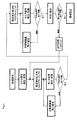
- FIG. 5 is a diagram illustrating the receiving device 300 according to the present embodiment.
- the receiving apparatus 300 includes a chromatic dispersion compensation circuit 101.
- the chromatic dispersion compensation circuit 101 is based on an analog-digital converter 11 that converts an optical analog waveform received from an optical fiber transmission path into a digital signal, and wavelength dispersion of the optical fiber transmission path that the digital signal output from the analog-digital converter 11 has.
- a digital signal processor 12 that compensates for waveform distortion with a dispersion compensation amount estimated by a chromatic dispersion amount estimation method described below, and a symbol arrival timing clock of received data included in the digital signal output from the analog-digital converter 11 And a symbol clock extractor 13 for extracting and outputting the intensity of the symbol arrival timing clock as a clock detection value.
- a rough estimation value estimated by a chromatic dispersion estimation method using a known signal or the like is set as an initial value in the dispersion compensation circuit.
- a waveform subjected to waveform distortion due to residual dispersion caused by an estimation error or the like is output from the dispersion compensation circuit.
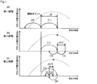
- D (k) represents the dispersion compensation amount set in the digital signal processor 12.
- S (0) a clock detection value
- the dispersion compensation amount D (0) is shifted in a negative direction by a certain shift amount ⁇ D (dispersion compensation amount D (0) ⁇ ), and the clock detection value S ( Measure and store 0-).
- the constant shift amount ⁇ D is about the maximum value of the deviation amount from the expected value of the initial value.
- the initial value depends on the rough estimation algorithm to be used (for example, the algorithm of Patent Document 4). For example, assuming that the error is 1.5 to 5% of the dispersion amount 20000 psec / nm exemplified as the compensation range in Patent Document 4, ⁇ D is set to 300 to 1000 psec / nm.
- the shift amount ⁇ D / 4 is shifted in the positive and negative directions around the compensation dispersion amount D (2) [5] [6].
- the respective clock synchronization detection signals S (2+) and S (2-) when the dispersion compensation amount is shifted to positive and negative are detected and stored in the memory. Then, both are compared and shifted in a larger code direction. Thereafter, by repeating the same process, the optimum compensation dispersion amount can be made asymptotic.
- the shift amount of the compensation dispersion amount D (k) at the k-th stage is ⁇ D / (2 (k ⁇ 1) ), and is halved each time the process proceeds.
- the detection signal originally includes an error
- S (k) is set again.
- S (k) is set again.
- shifting based on uncertain information can reduce the risk of causing an unstable operation.
- the shift amount of the compensation dispersion amount D (k) is halved for each step, that is, ⁇ D / (2 (k ⁇ 1) ), but the shift amount is ⁇ D / (M (k ⁇ 1) ) ) (M is a real number of 1 or more).
- the dispersion compensation amount setting value is determined based on one measurement value of the clock detection signal at each setting value. Therefore, when the error of S (k) in each measurement is large, the optimization sequence may be unstable.
- a method for stabilization measure multiple times at different times for each set value, and compare the average value to determine which direction of positive or negative sign should be used for stable operation. Is expected.
- the coarse estimation value of the dispersion estimation circuit is used as the initial value of the dispersion compensation amount.
- a dispersion value given from the outside may be set.
- a case where the dispersion amount of the transmission line is previously measured with a dispersion measuring device or the like can be considered.
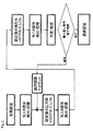
- FIG. 3 is a diagram for explaining the fine adjustment process of the present embodiment.
- a coarse compensation dispersion compensation amount D (0) estimated by a chromatic dispersion estimation method using a known signal or the like is set as an initial value in the dispersion compensation circuit.
- most of the chromatic dispersion is compensated, and a waveform subjected to waveform distortion due to residual dispersion caused by an estimation error or the like is output from the dispersion compensation circuit.
- the clock-synchronized clock detection value S (0) at the initially set dispersion compensation amount D (0) is measured and stored.
- the dispersion compensation set value is shifted in the positive direction by a small amount ⁇ D from D (0) as the first step.
- the clock detection value S (0 + ⁇ ) synchronized with the clock is measured and stored. Further, shifting in the positive direction by ⁇ D, and measuring clock-synchronized clock detection values S (0 + 2 ⁇ ), S (0 + 3 ⁇ ),..., S (0 + n ⁇ ) at the points 2 ⁇ D, 3 ⁇ D,. It may be stored in a memory.
- ⁇ D is shifted in the negative direction, and the clock detection value S (0 ⁇ ) of the clock synchronization at that time is measured and stored in the memory. Similarly, it is shifted in the negative direction by ⁇ D, and at the points ⁇ 2 ⁇ D, ⁇ 3 ⁇ D,..., The clock detection values S (0-2 ⁇ ), S (0-3 ⁇ ),. S (0 ⁇ n ⁇ ) may be measured and stored in the memory.
- a control block diagram of this part is shown in FIG. Repeat this N times.
- an example in which the number of equal points is measured with respect to positive and negative is shown, but it is not necessary to be particularly equal to positive and negative. For example, only D (0) and D (0) + ⁇ D may be measured.
- the minute amount ⁇ D is set based on the period and amplitude of the ripple generated in the clock detection value S (k) with respect to the dispersion compensation amount in FIG. Specifically, the minute amount ⁇ D may be set to be equal to or less than the ripple period. For example, when the amplitude of the ripple is about 10% of the clock detection value S (k), the average fluctuation amount of the clock detection value S (k) when the set dispersion compensation amount D (k) is shifted by ⁇ D is the clock. It is less than 10% of the detected value S (k). When the ripple period changes depending on conditions, the minute amount ⁇ D is made sufficiently smaller than the standard deviation of the final target error.
- ⁇ D can be set to 1/3 to 1/50 of the target error, preferably 1/5 to 1/20, and more preferably 1/7 to 1/20.
- the final target error is 50 psec / nm to 150 psec / nm
- ⁇ D is set to about 1 psec / nm to 50 psec / nm, preferably about 4 psec / nm to 30 psec / nm.
- ⁇ D when ⁇ D is changed according to k, it is changed to ⁇ D / (2 (k ⁇ 1) ) similarly to ⁇ D.
- ⁇ D can be set to 1/3 to 1/50 of ⁇ D, preferably 1/5 to 1/10, and more preferably 1/5 to 1/7.
- n.delta. +) and S (0. ⁇ .n.delta.-) are compared to comprehensively determine the sign direction in which the clock synchronization detection signal becomes large, and the dispersion compensation value is shifted.
- S (0 ⁇ n ⁇ ), S (0 ⁇ n ⁇ +), and S (0 ⁇ n ⁇ ) are averaged with respect to n, and each average value Savg (0) , Savg (0+), Savg (0 ⁇ ) are calculated.
- N is also set in consideration of the balance between accuracy and time.
- ⁇ D is fixed, it is limited by the relationship between ⁇ D and ⁇ D. If ⁇ D> ⁇ D / (2 (N ⁇ 1) ), the error cannot be reduced.
- N is set to 3 or more and 7 or less.
- the dispersion compensation amount D (1) is set to D (0) + ⁇ D.
- the dispersion compensation amount D (1) is set to D (0) ⁇ D.
- both Savg (0+) and Savg (0 ⁇ ) are smaller than Savg (0), it may be considered that Savg (0)> Savg (0+) and Savg (0)> Savg (0 ⁇ ).
- Is D (1) D (0).
- the control method after the second stage is the clock detection value at the point of dispersion compensation amount D (1), the point of D (1) + ⁇ D / 2, and the point of D (1) ⁇ D / 2.
- the positive / negative shift direction is performed using ⁇ D shifted in the positive / negative direction near each point and using the averaged clock detection values. Determine the direction.
- the dispersion compensation amount is shifted in the positive direction by the shift amount ⁇ D / 2 [1], and the dispersion compensation amount D (1) + ⁇ D / 2 is shifted in the positive and negative directions by a small amount n ⁇ ⁇ D to detect the clock.
- the value S (1 ⁇ n ⁇ +) is acquired [7] [8].
- Savg (1+) subjected to the averaging process is obtained.
- the dispersion compensation amount is shifted by a shift amount ⁇ D / 2 in the negative direction [2]
- the dispersion compensation amount D (1) ⁇ D / 2 is shifted by a minute amount n ⁇ ⁇ D in the positive and negative directions around the center.
- the clock detection value S (1 ⁇ n ⁇ ) is acquired. Further, using the detected values, Savg (1-) subjected to the averaging process is obtained.
- the positive / negative shift direction of the compensation dispersion amount is determined in the same manner as described above.
- a point where the compensation dispersion amount is D (2) a point shifted by a shift amount ⁇ D / 4 in the positive and negative directions around D (2), and these three points D (2) D (2) + ⁇ D / 4 D (2) - ⁇ D / 4 Comparison of the clock detection value at.
- the shift amount is further halved to ⁇ D / 4.
- S (1 ⁇ n ⁇ +) S (1 ⁇ n ⁇ -) To get.
- the average value Save (2) of these Savg (2+) Savg (2-) As described in the second step, the shift direction of the next step is determined.
- the optimum compensation dispersion amount can be made asymptotic.
- the shift amount at the k-th stage is ⁇ D / (2 (k ⁇ 1) ), which is halved as the process proceeds.
- the example in which the shift amount of the compensation dispersion amount D (k) is reduced by half, that is, ⁇ D / (2 (k ⁇ 1) ) has been described.
- the shift amount is ⁇ D as in the first embodiment. / (M (k-1) ).
- the minute amount for the averaging process is a constant value of ⁇ D. .
- the dispersion compensation amount cannot be optimized in units smaller than ⁇ D. Therefore, as the shift amount is halved to ⁇ D, ⁇ D / 2, ⁇ D / 4,...
- the minute amount ⁇ D may be reduced within a range where the averaging is effective. For example, the minute amount may be changed as small as ⁇ D, ⁇ D / 2, ⁇ D / 4,.
- a minute change is given to the compensation amount of the chromatic dispersion compensation circuit of the optical communication system, and this is given when searching for the optimum compensation amount using the clock detection signal as a monitor signal.
- the optimum dispersion compensation amount can be efficiently detected by reducing the change amount by half for each trial.
Landscapes
- Physics & Mathematics (AREA)
- Chemical & Material Sciences (AREA)
- Electromagnetism (AREA)
- Engineering & Computer Science (AREA)
- Computer Networks & Wireless Communication (AREA)
- Signal Processing (AREA)
- Dispersion Chemistry (AREA)
- Optics & Photonics (AREA)
- Analytical Chemistry (AREA)
- General Physics & Mathematics (AREA)
- Optical Communication System (AREA)
Abstract
Description
(1)任意の値を波長分散量の第1の候補値とするステップ、
(2)第1の候補値の近傍値を第2の候補値として複数抽出するステップ、
(3)各候補値に対応するデジタルクロック抽出信号強度を測定するステップ、
(4)複数の信号強度の増減の傾向から最適値(最大となる値)を抽出し、次の第1の候補値とするステップ、
(5)所定の条件を満たすまで、(2)~(4)を繰り返す判定ステップ、
を有することとした。
第k(kは整数)番目の分散補償量D(k)の初期値(k=0)である分散補償量D(0)を設定する初期値設定手順と、
受信データに含まれるシンボル到来タイミングクロックの分散補償量D(k)における強度をクロック検出値S(k)として検出し、記憶するクロック検出手順と、
前記分散補償量D(k)を所定量ΔDのM(k-1)分の1(Mは1以上の実数)だけプラス側にシフトした分散補償量D(k)+ΔD/M(k-1)における前記シンボル到来タイミングクロックの強度をクロック検出値S(k+)として検出し、記憶するプラス側シフト手順と、
前記分散補償量D(k)を所定量ΔDのM(k-1)分の1だけマイナス側にシフトした分散補償量D(k)-ΔD/M(k-1)における前記シンボル到来タイミングクロックの強度をクロック検出値S(k-)として検出し、記憶するマイナス側シフト手順と、
前記クロック検出値S(k)、前記クロック検出値S(k+)及び前記クロック検出値S(k-)を比較する比較手順と、
前記比較手順の結果、前記クロック検出値S(k)が最大である場合、前記分散補償量D(k)を最適分散補償量として決定して前記分散補償量の推定を完了し、前記クロック検出値S(k+)又は前記クロック検出値S(k-)が最大である場合、最大の前記クロック検出値の前記分散補償量を第k+1番目の分散補償量D(k+1)として前記クロック検出手順、前記プラス側シフト手順、前記マイナス側シフト手順及び前記比較手順を再度行うことを決定する判定手順と、
を行うことを特徴とする。
前記クロック検出手順において、前記分散補償量D(k)におけるクロック検出値S(k±0)、及び前記分散補償量D(k)を中心として分散補償量D(k)±nδD(nは自然数)におけるクロック検出値S(k±nδ)を検出し、
前記プラス側シフト手順において、前記分散補償量D(k)+ΔD/M(k-1)におけるクロック検出値S(k±0+)、及び前記分散補償量D(k)+ΔDを中心として分散補償量D(k)+ΔD/M(k-1)±nδD(nは自然数)におけるクロック検出値S(k±nδ+)を検出し、
前記マイナス側シフト手順において、前記分散補償量D(k)-ΔD/M(k-1)におけるクロック検出値S(k±0-)、及び前記分散補償量D(k)-ΔDを中心として分散補償量D(k)-ΔD/M(k-1)±nδD(nは自然数)におけるクロック検出値S(k±nδ-)を検出することを特徴とする。
クロック検出値S(k±0+)及びクロック検出値S(k±nδ+)を平均化して前記クロック検出値S(k+)とし、
クロック検出値S(k±0-)及びクロック検出値S(k±nδ-)を平均化して前記クロック検出値S(k-)とする
ことを特徴とする。
前記アナログデジタル変換器が出力する前記デジタル信号が持つ前記光ファイバ伝送路の波長分散による波形歪みを、前記波長分散量推定方法で推定した前記分散補償量で補償するデジタル信号処理器と、
前記アナログデジタル変換器が出力する前記デジタル信号に含まれる受信データのシンボル到来タイミングクロックを抽出し、前記シンボル到来タイミングクロックの強度を前記クロック検出値として出力するシンボルクロック抽出器と、
を備える。
まず、粗調整プロセスとして、既知信号を用いた波長分散推定法などによって推定された粗推定値を初期値として分散補償回路に設定する。このとき、波長分散の大部分が補償され、推定誤差などによって生じる残留分散による波形歪みを受けた波形が分散補償回路から出力される。
[1]分散補償量D(0)からある一定のシフト量ΔDだけ正の方向にシフトさせる(分散補償量D(0)+Δ)。そして、クロック同期のクロック検出値S(0+)を測定して記憶する。
[2]同様に、分散補償量D(0)からある一定のシフト量ΔDだけ負の方向にシフトさせ(分散補償量D(0)-Δ)、その際のクロック同期のクロック検出値S(0-)を測定して格納する。
一定のシフト量ΔDは、初期値が有する期待値からのずれ量の最大値程度とする。ここで、初期値は用いる粗推定アルゴリズム(例えば、特許文献4のアルゴリズム)に依存する。例えば、特許文献4で補償範囲として例示する分散量20000psec/nmの1.5~5%の誤差と仮定して、ΔDを300~1000psec/nmとする。
このように、シフト量をΔD/2,ΔD/4,ΔD/8,・・・と半減させてプロセスを繰り返すが、その反復回数は最終的な目標誤差範囲より、シフト量が小さくなるまでは繰り返す必要がある。例えば、ΔD=1024psec/nm、目標誤差50psec/nmとすると、シフト量はプロセス毎に1024、512、256、126、64、32、16(psec/nm)のように推移する。このため、シフト量が目標誤差より小さくなる6、7回程度、プロセスを繰り返す必要がある。時間に余裕があれば、シフト量がさらに小さくなるまでプロセスを繰り返してもよい。
クロック同期回路の検出信号の残留分散依存性が局所的に揺らぐ可能性がある。この場合、第一の実施例では、局所的な変化のために正方向にシフトすべきか、負方向にシフトすべきかの判断が困難となる場合がある。本実施形態は、局所的な残留分散依存性がある状況であっても、平均化することで高精度に分散補償量のシフト方向を判定し、安定的に分散補償量の推定を行うことができる。
微少量δDは、図3の分散補償量に対するクロック検出値S(k)に発生するリップルの周期及び振幅に基づいて設定する。具体的には、微少量δDはリップルの周期以下とすればよい。例えば、リップルの振幅がクロック検出値S(k)の10%程度である場合、設定分散補償量D(k)をδDシフトした際のクロック検出値S(k)の平均的な変動量はクロック検出値S(k)の10%未満とする。
また、リップルの周期が条件によって変化する場合、微少量δDは最終的な目標誤差の標準偏差より十分小さくする。例えば、δDは目標誤差の1/3~1/50、好ましくは1/5~1/20、より好ましくは1/7~1/20とすることができる。具体的数値として、最終的な目標誤差が50psec/nm~150psec/nmであれば、δDは1psec/nm~50psec/nm程度、好ましくは4psec/nm~30psec/nm程度に設定する。また、δDをkに従って変化させる場合、ΔDと同様にδD/(2(k-1))と変化させる。この場合、δDをΔDの1/3~1/50、好ましくは1/5~1/10、より好ましくは1/5~1/7とすることができる。

D(2)
D(2)+ΔD/4
D(2)-ΔD/4
でのクロック検出値の比較を実施する。第三段階では、シフト量がΔD/4と更に半減している。それら3ポイントにおいて、正負方向に微小量n×±δDづつシフト点のクロック検出値
S(1±nδ)
S(1±nδ+)
S(1±nδ-)
を取得する。さらに、これらの平均値
Save(2)
Savg(2+)
Savg(2-)
を求め、第二段階で説明したように次の段階のシフト方向を判断する。
12:デジタル信号処理器
13:シンボルクロック抽出器
15:光ファイバ
101:波長分散補償回路
300:受信装置
Claims (8)
- 光ファイバ伝送路の波長分散による波形歪みを補償する際の分散補償量を推定する波長分散量推定方法であって、
第k(kは整数)番目の分散補償量D(k)の初期値(k=0)である分散補償量D(0)を設定する初期値設定手順と、
受信データに含まれるシンボル到来タイミングクロックの分散補償量D(k)における強度をクロック検出値S(k)として検出し、記憶するクロック検出手順と、
前記分散補償量D(k)を所定量ΔDのM(k-1)分の1(Mは1以上の実数)だけプラス側にシフトした分散補償量D(k)+ΔD/M(k-1)における前記シンボル到来タイミングクロックの強度をクロック検出値S(k+)として検出し、記憶するプラス側シフト手順と、
前記分散補償量D(k)を所定量ΔDのM(k-1)分の1だけマイナス側にシフトした分散補償量D(k)-ΔD/M(k-1)における前記シンボル到来タイミングクロックの強度をクロック検出値S(k-)として検出し、記憶するマイナス側シフト手順と、
前記クロック検出値S(k)、前記クロック検出値S(k+)及び前記クロック検出値S(k-)を比較する比較手順と、
前記比較手順の結果、前記クロック検出値S(k)が最大である場合、前記分散補償量D(k)を最適分散補償量として決定して前記分散補償量の推定を完了し、前記クロック検出値S(k+)又は前記クロック検出値S(k-)が最大である場合、最大の前記クロック検出値の前記分散補償量を第k+1番目の分散補償量D(k+1)として前記クロック検出手順、前記プラス側シフト手順、前記マイナス側シフト手順及び前記比較手順を再度行うことを決定する判定手順と、
を行うことを特徴とする波長分散量推定方法。 - 前記初期値設定手順の前に前記分散補償量の概略値を取得し、前記分散補償量の概略値を前記初期値設定手順における前記分散補償量D(0)とする概略分散補償量取得手順を有することを特徴とする請求項1に記載の波長分散量推定方法。
- 前記クロック検出手順、前記プラス側シフト手順及び前記マイナス側シフト手順の少なくとも1つは、異なる時刻に複数回繰り返して平均化することを特徴とする請求項1又は2に記載の波長分散量推定方法。
- 前記プラス側シフト手順及び前記マイナス側シフト手順で前記分散補償量をシフトする前記所定量ΔDより小さい微少量δDが設定されており、
前記クロック検出手順において、前記分散補償量D(k)におけるクロック検出値S(k±0)、及び前記分散補償量D(k)を中心として分散補償量D(k)±nδD(nは自然数)におけるクロック検出値S(k±nδ)を検出し、
前記プラス側シフト手順において、前記分散補償量D(k)+ΔD/M(k-1)におけるクロック検出値S(k±0+)、及び前記分散補償量D(k)+ΔDを中心として分散補償量D(k)+ΔD/M(k-1)±nδD(nは自然数)におけるクロック検出値S(k±nδ+)を検出し、
前記マイナス側シフト手順において、前記分散補償量D(k)-ΔD/M(k-1)におけるクロック検出値S(k±0-)、及び前記分散補償量D(k)-ΔDを中心として分散補償量D(k)-ΔD/M(k-1)±nδD(nは自然数)におけるクロック検出値S(k±nδ-)を検出することを特徴とする請求項1又は2に記載の波長分散量推定方法。 - クロック検出値S(k±0)及びクロック検出値S(k±nδ)を平均化して前記クロック検出値S(k)とし、
クロック検出値S(k±0+)及びクロック検出値S(k±nδ+)を平均化して前記クロック検出値S(k+)とし、
クロック検出値S(k±0-)及びクロック検出値S(k±nδ-)を平均化して前記クロック検出値S(k-)とする
ことを特徴とする請求項4に記載の波長分散量推定方法。 - 前記判定手順で、前記クロック検出値S(k)と前記クロック検出値S(k+)との差及び前記クロック検出値S(k)と前記クロック検出値S(k-)との差が所定の閾値未満の場合、前記分散補償量D(k)を最適分散補償量として決定して前記分散補償量の推定を完了することを特徴とする請求項1又は2に記載の波長分散量推定方法。
- 前記光ファイバ伝送路から受信した光アナログ波形をデジタル信号に変換するアナログデジタル変換器と、
前記アナログデジタル変換器が出力する前記デジタル信号が持つ前記光ファイバ伝送路の波長分散による波形歪みを、請求項1から6のいずれかに記載の波長分散量推定方法で推定した前記分散補償量で補償するデジタル信号処理器と、
前記アナログデジタル変換器が出力する前記デジタル信号に含まれる受信データのシンボル到来タイミングクロックを抽出し、前記シンボル到来タイミングクロックの強度を前記クロック検出値として出力するシンボルクロック抽出器と、
を備える波長分散補償回路。 - 請求項7に記載の波長分散補償回路を含む受信装置。
Priority Applications (3)
| Application Number | Priority Date | Filing Date | Title |
|---|---|---|---|
| JP2012555941A JP5663606B2 (ja) | 2011-02-01 | 2012-02-01 | 波長分散量推定方法、波長分散補償回路、及び受信装置 |
| CN201280007278.0A CN103404051B (zh) | 2011-02-01 | 2012-02-01 | 波长色散量推算方法、波长色散补偿电路以及接收装置 |
| US13/982,507 US8971703B2 (en) | 2011-02-01 | 2012-02-01 | Wavelength dispersion amount estimation method, wavelength dispersion compensation circuit, and reception device |
Applications Claiming Priority (2)
| Application Number | Priority Date | Filing Date | Title |
|---|---|---|---|
| JP2011-019499 | 2011-02-01 | ||
| JP2011019499 | 2011-02-01 |
Publications (1)
| Publication Number | Publication Date |
|---|---|
| WO2012105628A1 true WO2012105628A1 (ja) | 2012-08-09 |
Family
ID=46602834
Family Applications (1)
| Application Number | Title | Priority Date | Filing Date |
|---|---|---|---|
| PCT/JP2012/052318 Ceased WO2012105628A1 (ja) | 2011-02-01 | 2012-02-01 | 波長分散量推定方法、波長分散補償回路、及び受信装置 |
Country Status (4)
| Country | Link |
|---|---|
| US (1) | US8971703B2 (ja) |
| JP (1) | JP5663606B2 (ja) |
| CN (1) | CN103404051B (ja) |
| WO (1) | WO2012105628A1 (ja) |
Cited By (1)
| Publication number | Priority date | Publication date | Assignee | Title |
|---|---|---|---|---|
| US10422719B2 (en) | 2015-11-05 | 2019-09-24 | Ntt Electronics Corporation | Chromatic dispersion estimating circuit, optical reception device and chromatic dispersion amount estimating method |
Citations (3)
| Publication number | Priority date | Publication date | Assignee | Title |
|---|---|---|---|---|
| WO1999048231A1 (en) * | 1998-03-19 | 1999-09-23 | Fujitsu Limited | Wavelength dispersion equalizing method and device |
| WO2007141846A1 (ja) * | 2006-06-06 | 2007-12-13 | Fujitsu Limited | 分散補償制御装置および分散制御量探索方法 |
| JP2010178222A (ja) * | 2009-01-30 | 2010-08-12 | Fujitsu Ltd | 歪み補償装置,光受信装置及び光送受信システム |
Family Cites Families (7)
| Publication number | Priority date | Publication date | Assignee | Title |
|---|---|---|---|---|
| JP3771755B2 (ja) | 1999-08-11 | 2006-04-26 | 日本電信電話株式会社 | 光自動等化器 |
| US7536108B2 (en) * | 2001-06-29 | 2009-05-19 | Nippon Telegraph & Telephone Corporation | High precision chromatic dispersion measuring method and automatic dispersion compensating optical link system that uses this method |
| JP4516907B2 (ja) * | 2005-08-26 | 2010-08-04 | 富士通株式会社 | 光受信装置およびその制御方法 |
| JP4826462B2 (ja) * | 2006-12-20 | 2011-11-30 | 株式会社日立製作所 | 分散補償器、光伝送システム及び光伝送方法 |
| JP5004181B2 (ja) | 2008-01-11 | 2012-08-22 | Kddi株式会社 | 領域識別装置およびコンテンツ識別装置 |
| WO2009144997A1 (ja) | 2008-05-27 | 2009-12-03 | 日本電気株式会社 | 光ファイバの分散検出装置およびそれを用いた自動分散補償システム |
| WO2011007803A1 (ja) | 2009-07-17 | 2011-01-20 | 日本電信電話株式会社 | 波長分散量算出装置、光信号受信装置、光信号送信装置及び波長分散量算出方法 |
-
2012
- 2012-02-01 US US13/982,507 patent/US8971703B2/en active Active
- 2012-02-01 CN CN201280007278.0A patent/CN103404051B/zh active Active
- 2012-02-01 WO PCT/JP2012/052318 patent/WO2012105628A1/ja not_active Ceased
- 2012-02-01 JP JP2012555941A patent/JP5663606B2/ja active Active
Patent Citations (3)
| Publication number | Priority date | Publication date | Assignee | Title |
|---|---|---|---|---|
| WO1999048231A1 (en) * | 1998-03-19 | 1999-09-23 | Fujitsu Limited | Wavelength dispersion equalizing method and device |
| WO2007141846A1 (ja) * | 2006-06-06 | 2007-12-13 | Fujitsu Limited | 分散補償制御装置および分散制御量探索方法 |
| JP2010178222A (ja) * | 2009-01-30 | 2010-08-12 | Fujitsu Ltd | 歪み補償装置,光受信装置及び光送受信システム |
Cited By (1)
| Publication number | Priority date | Publication date | Assignee | Title |
|---|---|---|---|---|
| US10422719B2 (en) | 2015-11-05 | 2019-09-24 | Ntt Electronics Corporation | Chromatic dispersion estimating circuit, optical reception device and chromatic dispersion amount estimating method |
Also Published As
| Publication number | Publication date |
|---|---|
| CN103404051A (zh) | 2013-11-20 |
| US8971703B2 (en) | 2015-03-03 |
| JPWO2012105628A1 (ja) | 2014-07-03 |
| US20130343749A1 (en) | 2013-12-26 |
| JP5663606B2 (ja) | 2015-02-04 |
| CN103404051B (zh) | 2016-06-01 |
Similar Documents
| Publication | Publication Date | Title |
|---|---|---|
| US7822350B2 (en) | Reconstruction and restoration of two polarization components of an optical signal field | |
| CN100539472C (zh) | 信号波形劣化补偿器 | |
| US9686020B2 (en) | Signal processing device and signal processing method | |
| US8145071B2 (en) | Electrical-dispersion compensating apparatus, optical receiving apparatus, and optical receiving method | |
| JP5012811B2 (ja) | 分散検出装置およびそれを用いた自動分散補償システム | |
| US8903255B2 (en) | Polarization-multiplexed signal receiver, polarization multiplexing system and polarization-multiplexed signal receiving method | |
| JP2010504694A (ja) | 光信号フィールドの復元および修復 | |
| JP5495120B2 (ja) | 光受信装置、光受信方法及び光受信装置の制御プログラム | |
| JP5263289B2 (ja) | 光ファイバの分散検出装置およびそれを用いた自動分散補償システム | |
| JP5663604B2 (ja) | 波長分散量推定方法、波長分散補償回路、及び受信装置 | |
| US12438610B2 (en) | Device and method for estimating characteristics of optical fiber transmission line | |
| JP5663606B2 (ja) | 波長分散量推定方法、波長分散補償回路、及び受信装置 | |
| US11742978B2 (en) | Optical network device and method for monitoring transmission line | |
| Wang et al. | Performance Enhancement of the High-Order QAM Transmission-Based Kerr Non-Linearity Coefficient Estimation Scheme for Hollow-Core Fibers | |
| CN105509885B (zh) | 用于测量光信号的线宽的系统和方法 | |
| CN119582967B (zh) | 一种模分复用光纤通信的信噪比与模式耦合联合估计方法、装置和存储介质 | |
| CN110971302B (zh) | 一种低速延时采样估计光纤色散的装置与方法 | |
| Wu et al. | Wavelength Dispersion Amount Estimation Method Compensation Circuit and Reception Device | |
| Zhou et al. | Implement Digital Longitudinal Monitoring for Intelligent Optical Networks | |
| CN122027025A (zh) | 光纤传输链路质量监测与色散补偿优化方法及系统 | |
| Yu et al. | Optical performance monitoring based on 2-D phase portrait generated by single-channel sampling technique | |
| KR20160131666A (ko) | 비선형 광전송 시스템을 위한 광신호대 잡음비 추정 방법 및 장치 |
Legal Events
| Date | Code | Title | Description |
|---|---|---|---|
| 121 | Ep: the epo has been informed by wipo that ep was designated in this application |
Ref document number: 12742159 Country of ref document: EP Kind code of ref document: A1 |
|
| ENP | Entry into the national phase |
Ref document number: 2012555941 Country of ref document: JP Kind code of ref document: A |
|
| NENP | Non-entry into the national phase |
Ref country code: DE |
|
| WWE | Wipo information: entry into national phase |
Ref document number: 13982507 Country of ref document: US |
|
| 122 | Ep: pct application non-entry in european phase |
Ref document number: 12742159 Country of ref document: EP Kind code of ref document: A1 |