WO2012105473A1 - Bonded-substrate fabrication method, bonded substrate, substrate bonding method, bonded-substrate fabrication device, and substrate assembly - Google Patents
Bonded-substrate fabrication method, bonded substrate, substrate bonding method, bonded-substrate fabrication device, and substrate assembly Download PDFInfo
- Publication number
- WO2012105473A1 WO2012105473A1 PCT/JP2012/051935 JP2012051935W WO2012105473A1 WO 2012105473 A1 WO2012105473 A1 WO 2012105473A1 JP 2012051935 W JP2012051935 W JP 2012051935W WO 2012105473 A1 WO2012105473 A1 WO 2012105473A1
- Authority
- WO
- WIPO (PCT)
- Prior art keywords
- substrate
- bonding
- metal
- particle source
- particles
- Prior art date
Links
- 239000000758 substrate Substances 0.000 title claims abstract description 684
- 238000000034 method Methods 0.000 title claims abstract description 176
- 238000004519 manufacturing process Methods 0.000 title claims description 115
- 239000002245 particle Substances 0.000 claims abstract description 374
- 239000002923 metal particle Substances 0.000 claims abstract description 157
- 229910052710 silicon Inorganic materials 0.000 claims abstract description 116
- 239000010703 silicon Substances 0.000 claims abstract description 114
- 230000008569 process Effects 0.000 claims description 111
- 238000004381 surface treatment Methods 0.000 claims description 106
- 229910052751 metal Inorganic materials 0.000 claims description 96
- 239000002184 metal Substances 0.000 claims description 96
- XEEYBQQBJWHFJM-UHFFFAOYSA-N Iron Chemical group [Fe] XEEYBQQBJWHFJM-UHFFFAOYSA-N 0.000 claims description 84
- 239000000463 material Substances 0.000 claims description 69
- 239000010410 layer Substances 0.000 claims description 57
- 239000002344 surface layer Substances 0.000 claims description 56
- 230000005855 radiation Effects 0.000 claims description 46
- 229910052742 iron Inorganic materials 0.000 claims description 35
- 230000007246 mechanism Effects 0.000 claims description 35
- 238000005304 joining Methods 0.000 claims description 29
- 230000001678 irradiating effect Effects 0.000 claims description 18
- 238000009826 distribution Methods 0.000 claims description 13
- 229910052723 transition metal Inorganic materials 0.000 claims description 10
- 150000003624 transition metals Chemical group 0.000 claims description 10
- 230000004044 response Effects 0.000 claims description 7
- 238000004886 process control Methods 0.000 claims description 6
- XUIMIQQOPSSXEZ-UHFFFAOYSA-N Silicon Chemical compound [Si] XUIMIQQOPSSXEZ-UHFFFAOYSA-N 0.000 abstract description 118
- 239000010409 thin film Substances 0.000 abstract description 42
- 239000010408 film Substances 0.000 description 28
- XKRFYHLGVUSROY-UHFFFAOYSA-N Argon Chemical compound [Ar] XKRFYHLGVUSROY-UHFFFAOYSA-N 0.000 description 27
- 230000001133 acceleration Effects 0.000 description 24
- 238000005259 measurement Methods 0.000 description 22
- 238000010586 diagram Methods 0.000 description 18
- 229910052786 argon Inorganic materials 0.000 description 15
- 230000015572 biosynthetic process Effects 0.000 description 14
- VYPSYNLAJGMNEJ-UHFFFAOYSA-N Silicium dioxide Chemical compound O=[Si]=O VYPSYNLAJGMNEJ-UHFFFAOYSA-N 0.000 description 12
- 239000012535 impurity Substances 0.000 description 12
- 238000002360 preparation method Methods 0.000 description 12
- 229910052814 silicon oxide Inorganic materials 0.000 description 12
- 229910052581 Si3N4 Inorganic materials 0.000 description 11
- 238000003384 imaging method Methods 0.000 description 11
- 235000012431 wafers Nutrition 0.000 description 11
- 239000013590 bulk material Substances 0.000 description 10
- 238000005530 etching Methods 0.000 description 10
- 238000007254 oxidation reaction Methods 0.000 description 8
- 238000001994 activation Methods 0.000 description 7
- 230000005540 biological transmission Effects 0.000 description 7
- 238000009792 diffusion process Methods 0.000 description 7
- 238000010438 heat treatment Methods 0.000 description 7
- 230000003287 optical effect Effects 0.000 description 7
- 230000003647 oxidation Effects 0.000 description 7
- HQVNEWCFYHHQES-UHFFFAOYSA-N silicon nitride Chemical compound N12[Si]34N5[Si]62N3[Si]51N64 HQVNEWCFYHHQES-UHFFFAOYSA-N 0.000 description 7
- 239000000126 substance Substances 0.000 description 7
- 238000012545 processing Methods 0.000 description 6
- 239000011800 void material Substances 0.000 description 6
- 239000013078 crystal Substances 0.000 description 5
- 230000000694 effects Effects 0.000 description 5
- 230000005684 electric field Effects 0.000 description 5
- 241000252073 Anguilliformes Species 0.000 description 4
- QVGXLLKOCUKJST-UHFFFAOYSA-N atomic oxygen Chemical compound [O] QVGXLLKOCUKJST-UHFFFAOYSA-N 0.000 description 4
- 238000005430 electron energy loss spectroscopy Methods 0.000 description 4
- 239000011261 inert gas Substances 0.000 description 4
- 238000010884 ion-beam technique Methods 0.000 description 4
- 230000007935 neutral effect Effects 0.000 description 4
- 239000001301 oxygen Substances 0.000 description 4
- 229910052760 oxygen Inorganic materials 0.000 description 4
- 239000004065 semiconductor Substances 0.000 description 4
- 239000011343 solid material Substances 0.000 description 4
- 238000004627 transmission electron microscopy Methods 0.000 description 4
- 230000004913 activation Effects 0.000 description 3
- -1 argon ions Chemical class 0.000 description 3
- 230000000052 comparative effect Effects 0.000 description 3
- 230000006870 function Effects 0.000 description 3
- 238000012966 insertion method Methods 0.000 description 3
- 150000002500 ions Chemical class 0.000 description 3
- 238000001228 spectrum Methods 0.000 description 3
- 238000004544 sputter deposition Methods 0.000 description 3
- 238000011282 treatment Methods 0.000 description 3
- IJGRMHOSHXDMSA-UHFFFAOYSA-N Atomic nitrogen Chemical compound N#N IJGRMHOSHXDMSA-UHFFFAOYSA-N 0.000 description 2
- 229910000676 Si alloy Inorganic materials 0.000 description 2
- 229910004298 SiO 2 Inorganic materials 0.000 description 2
- 230000009471 action Effects 0.000 description 2
- 230000003213 activating effect Effects 0.000 description 2
- 238000004458 analytical method Methods 0.000 description 2
- 238000000429 assembly Methods 0.000 description 2
- 230000000712 assembly Effects 0.000 description 2
- 230000008901 benefit Effects 0.000 description 2
- 238000006243 chemical reaction Methods 0.000 description 2
- 238000001514 detection method Methods 0.000 description 2
- 229910003460 diamond Inorganic materials 0.000 description 2
- 239000010432 diamond Substances 0.000 description 2
- 238000011156 evaluation Methods 0.000 description 2
- 239000000284 extract Substances 0.000 description 2
- 239000007789 gas Substances 0.000 description 2
- 239000011521 glass Substances 0.000 description 2
- 239000007769 metal material Substances 0.000 description 2
- 239000012466 permeate Substances 0.000 description 2
- 238000005240 physical vapour deposition Methods 0.000 description 2
- 230000001737 promoting effect Effects 0.000 description 2
- 238000000926 separation method Methods 0.000 description 2
- 239000002210 silicon-based material Substances 0.000 description 2
- 238000003917 TEM image Methods 0.000 description 1
- 238000005411 Van der Waals force Methods 0.000 description 1
- 230000002411 adverse Effects 0.000 description 1
- 238000005280 amorphization Methods 0.000 description 1
- 229910021417 amorphous silicon Inorganic materials 0.000 description 1
- 238000013459 approach Methods 0.000 description 1
- 229910001423 beryllium ion Inorganic materials 0.000 description 1
- 230000015556 catabolic process Effects 0.000 description 1
- 239000000919 ceramic Substances 0.000 description 1
- 238000005229 chemical vapour deposition Methods 0.000 description 1
- 238000004140 cleaning Methods 0.000 description 1
- 238000004891 communication Methods 0.000 description 1
- 229910021419 crystalline silicon Inorganic materials 0.000 description 1
- 230000006378 damage Effects 0.000 description 1
- 230000003247 decreasing effect Effects 0.000 description 1
- 238000000151 deposition Methods 0.000 description 1
- 230000008021 deposition Effects 0.000 description 1
- 239000003989 dielectric material Substances 0.000 description 1
- 239000010419 fine particle Substances 0.000 description 1
- 230000006872 improvement Effects 0.000 description 1
- 238000003780 insertion Methods 0.000 description 1
- 230000037431 insertion Effects 0.000 description 1
- 238000009434 installation Methods 0.000 description 1
- 239000011159 matrix material Substances 0.000 description 1
- 238000002844 melting Methods 0.000 description 1
- 230000008018 melting Effects 0.000 description 1
- 229910021645 metal ion Inorganic materials 0.000 description 1
- 239000000203 mixture Substances 0.000 description 1
- 238000012986 modification Methods 0.000 description 1
- 230000004048 modification Effects 0.000 description 1
- 150000004767 nitrides Chemical class 0.000 description 1
- 229910052757 nitrogen Inorganic materials 0.000 description 1
- 229910052755 nonmetal Inorganic materials 0.000 description 1
- 239000011368 organic material Substances 0.000 description 1
- RJCRUVXAWQRZKQ-UHFFFAOYSA-N oxosilicon;silicon Chemical compound [Si].[Si]=O RJCRUVXAWQRZKQ-UHFFFAOYSA-N 0.000 description 1
- 238000007781 pre-processing Methods 0.000 description 1
- 238000003672 processing method Methods 0.000 description 1
- 239000000047 product Substances 0.000 description 1
- 230000002040 relaxant effect Effects 0.000 description 1
- 238000007789 sealing Methods 0.000 description 1
- SBEQWOXEGHQIMW-UHFFFAOYSA-N silicon Chemical compound [Si].[Si] SBEQWOXEGHQIMW-UHFFFAOYSA-N 0.000 description 1
- 239000011856 silicon-based particle Substances 0.000 description 1
- 229910000679 solder Inorganic materials 0.000 description 1
- 239000007790 solid phase Substances 0.000 description 1
- 230000003595 spectral effect Effects 0.000 description 1
- 239000007858 starting material Substances 0.000 description 1
- WFKWXMTUELFFGS-UHFFFAOYSA-N tungsten Chemical compound [W] WFKWXMTUELFFGS-UHFFFAOYSA-N 0.000 description 1
- 229910052721 tungsten Inorganic materials 0.000 description 1
- 239000010937 tungsten Substances 0.000 description 1
- XLYOFNOQVPJJNP-UHFFFAOYSA-N water Substances O XLYOFNOQVPJJNP-UHFFFAOYSA-N 0.000 description 1
Images


Classifications
-
- H—ELECTRICITY
- H01—ELECTRIC ELEMENTS
- H01L—SEMICONDUCTOR DEVICES NOT COVERED BY CLASS H10
- H01L21/00—Processes or apparatus adapted for the manufacture or treatment of semiconductor or solid state devices or of parts thereof
- H01L21/02—Manufacture or treatment of semiconductor devices or of parts thereof
- H01L21/04—Manufacture or treatment of semiconductor devices or of parts thereof the devices having at least one potential-jump barrier or surface barrier, e.g. PN junction, depletion layer or carrier concentration layer
- H01L21/18—Manufacture or treatment of semiconductor devices or of parts thereof the devices having at least one potential-jump barrier or surface barrier, e.g. PN junction, depletion layer or carrier concentration layer the devices having semiconductor bodies comprising elements of Group IV of the Periodic System or AIIIBV compounds with or without impurities, e.g. doping materials
- H01L21/30—Treatment of semiconductor bodies using processes or apparatus not provided for in groups H01L21/20 - H01L21/26
- H01L21/322—Treatment of semiconductor bodies using processes or apparatus not provided for in groups H01L21/20 - H01L21/26 to modify their internal properties, e.g. to produce internal imperfections
- H01L21/3221—Treatment of semiconductor bodies using processes or apparatus not provided for in groups H01L21/20 - H01L21/26 to modify their internal properties, e.g. to produce internal imperfections of silicon bodies, e.g. for gettering
-
- H—ELECTRICITY
- H01—ELECTRIC ELEMENTS
- H01L—SEMICONDUCTOR DEVICES NOT COVERED BY CLASS H10
- H01L21/00—Processes or apparatus adapted for the manufacture or treatment of semiconductor or solid state devices or of parts thereof
- H01L21/02—Manufacture or treatment of semiconductor devices or of parts thereof
- H01L21/04—Manufacture or treatment of semiconductor devices or of parts thereof the devices having at least one potential-jump barrier or surface barrier, e.g. PN junction, depletion layer or carrier concentration layer
- H01L21/18—Manufacture or treatment of semiconductor devices or of parts thereof the devices having at least one potential-jump barrier or surface barrier, e.g. PN junction, depletion layer or carrier concentration layer the devices having semiconductor bodies comprising elements of Group IV of the Periodic System or AIIIBV compounds with or without impurities, e.g. doping materials
- H01L21/20—Deposition of semiconductor materials on a substrate, e.g. epitaxial growth solid phase epitaxy
-
- B—PERFORMING OPERATIONS; TRANSPORTING
- B23—MACHINE TOOLS; METAL-WORKING NOT OTHERWISE PROVIDED FOR
- B23K—SOLDERING OR UNSOLDERING; WELDING; CLADDING OR PLATING BY SOLDERING OR WELDING; CUTTING BY APPLYING HEAT LOCALLY, e.g. FLAME CUTTING; WORKING BY LASER BEAM
- B23K1/00—Soldering, e.g. brazing, or unsoldering
- B23K1/20—Preliminary treatment of work or areas to be soldered, e.g. in respect of a galvanic coating
-
- B—PERFORMING OPERATIONS; TRANSPORTING
- B23—MACHINE TOOLS; METAL-WORKING NOT OTHERWISE PROVIDED FOR
- B23K—SOLDERING OR UNSOLDERING; WELDING; CLADDING OR PLATING BY SOLDERING OR WELDING; CUTTING BY APPLYING HEAT LOCALLY, e.g. FLAME CUTTING; WORKING BY LASER BEAM
- B23K20/00—Non-electric welding by applying impact or other pressure, with or without the application of heat, e.g. cladding or plating
- B23K20/16—Non-electric welding by applying impact or other pressure, with or without the application of heat, e.g. cladding or plating with interposition of special material to facilitate connection of the parts, e.g. material for absorbing or producing gas
-
- B—PERFORMING OPERATIONS; TRANSPORTING
- B23—MACHINE TOOLS; METAL-WORKING NOT OTHERWISE PROVIDED FOR
- B23K—SOLDERING OR UNSOLDERING; WELDING; CLADDING OR PLATING BY SOLDERING OR WELDING; CUTTING BY APPLYING HEAT LOCALLY, e.g. FLAME CUTTING; WORKING BY LASER BEAM
- B23K20/00—Non-electric welding by applying impact or other pressure, with or without the application of heat, e.g. cladding or plating
- B23K20/24—Preliminary treatment
-
- H—ELECTRICITY
- H01—ELECTRIC ELEMENTS
- H01J—ELECTRIC DISCHARGE TUBES OR DISCHARGE LAMPS
- H01J37/00—Discharge tubes with provision for introducing objects or material to be exposed to the discharge, e.g. for the purpose of examination or processing thereof
- H01J37/30—Electron-beam or ion-beam tubes for localised treatment of objects
- H01J37/317—Electron-beam or ion-beam tubes for localised treatment of objects for changing properties of the objects or for applying thin layers thereon, e.g. for ion implantation
-
- H—ELECTRICITY
- H01—ELECTRIC ELEMENTS
- H01L—SEMICONDUCTOR DEVICES NOT COVERED BY CLASS H10
- H01L21/00—Processes or apparatus adapted for the manufacture or treatment of semiconductor or solid state devices or of parts thereof
- H01L21/02—Manufacture or treatment of semiconductor devices or of parts thereof
- H01L21/02041—Cleaning
- H01L21/02043—Cleaning before device manufacture, i.e. Begin-Of-Line process
- H01L21/02046—Dry cleaning only
-
- H—ELECTRICITY
- H01—ELECTRIC ELEMENTS
- H01L—SEMICONDUCTOR DEVICES NOT COVERED BY CLASS H10
- H01L21/00—Processes or apparatus adapted for the manufacture or treatment of semiconductor or solid state devices or of parts thereof
- H01L21/02—Manufacture or treatment of semiconductor devices or of parts thereof
- H01L21/04—Manufacture or treatment of semiconductor devices or of parts thereof the devices having at least one potential-jump barrier or surface barrier, e.g. PN junction, depletion layer or carrier concentration layer
- H01L21/18—Manufacture or treatment of semiconductor devices or of parts thereof the devices having at least one potential-jump barrier or surface barrier, e.g. PN junction, depletion layer or carrier concentration layer the devices having semiconductor bodies comprising elements of Group IV of the Periodic System or AIIIBV compounds with or without impurities, e.g. doping materials
- H01L21/20—Deposition of semiconductor materials on a substrate, e.g. epitaxial growth solid phase epitaxy
- H01L21/2003—Deposition of semiconductor materials on a substrate, e.g. epitaxial growth solid phase epitaxy characterised by the substrate
- H01L21/2007—Bonding of semiconductor wafers to insulating substrates or to semiconducting substrates using an intermediate insulating layer
-
- H—ELECTRICITY
- H01—ELECTRIC ELEMENTS
- H01L—SEMICONDUCTOR DEVICES NOT COVERED BY CLASS H10
- H01L21/00—Processes or apparatus adapted for the manufacture or treatment of semiconductor or solid state devices or of parts thereof
- H01L21/02—Manufacture or treatment of semiconductor devices or of parts thereof
- H01L21/04—Manufacture or treatment of semiconductor devices or of parts thereof the devices having at least one potential-jump barrier or surface barrier, e.g. PN junction, depletion layer or carrier concentration layer
- H01L21/18—Manufacture or treatment of semiconductor devices or of parts thereof the devices having at least one potential-jump barrier or surface barrier, e.g. PN junction, depletion layer or carrier concentration layer the devices having semiconductor bodies comprising elements of Group IV of the Periodic System or AIIIBV compounds with or without impurities, e.g. doping materials
- H01L21/26—Bombardment with radiation
- H01L21/263—Bombardment with radiation with high-energy radiation
-
- H—ELECTRICITY
- H01—ELECTRIC ELEMENTS
- H01L—SEMICONDUCTOR DEVICES NOT COVERED BY CLASS H10
- H01L21/00—Processes or apparatus adapted for the manufacture or treatment of semiconductor or solid state devices or of parts thereof
- H01L21/02—Manufacture or treatment of semiconductor devices or of parts thereof
- H01L21/04—Manufacture or treatment of semiconductor devices or of parts thereof the devices having at least one potential-jump barrier or surface barrier, e.g. PN junction, depletion layer or carrier concentration layer
- H01L21/18—Manufacture or treatment of semiconductor devices or of parts thereof the devices having at least one potential-jump barrier or surface barrier, e.g. PN junction, depletion layer or carrier concentration layer the devices having semiconductor bodies comprising elements of Group IV of the Periodic System or AIIIBV compounds with or without impurities, e.g. doping materials
- H01L21/30—Treatment of semiconductor bodies using processes or apparatus not provided for in groups H01L21/20 - H01L21/26
- H01L21/302—Treatment of semiconductor bodies using processes or apparatus not provided for in groups H01L21/20 - H01L21/26 to change their surface-physical characteristics or shape, e.g. etching, polishing, cutting
-
- H—ELECTRICITY
- H01—ELECTRIC ELEMENTS
- H01L—SEMICONDUCTOR DEVICES NOT COVERED BY CLASS H10
- H01L21/00—Processes or apparatus adapted for the manufacture or treatment of semiconductor or solid state devices or of parts thereof
- H01L21/67—Apparatus specially adapted for handling semiconductor or electric solid state devices during manufacture or treatment thereof; Apparatus specially adapted for handling wafers during manufacture or treatment of semiconductor or electric solid state devices or components ; Apparatus not specifically provided for elsewhere
- H01L21/67005—Apparatus not specifically provided for elsewhere
- H01L21/67011—Apparatus for manufacture or treatment
- H01L21/67092—Apparatus for mechanical treatment
-
- H—ELECTRICITY
- H01—ELECTRIC ELEMENTS
- H01L—SEMICONDUCTOR DEVICES NOT COVERED BY CLASS H10
- H01L21/00—Processes or apparatus adapted for the manufacture or treatment of semiconductor or solid state devices or of parts thereof
- H01L21/67—Apparatus specially adapted for handling semiconductor or electric solid state devices during manufacture or treatment thereof; Apparatus specially adapted for handling wafers during manufacture or treatment of semiconductor or electric solid state devices or components ; Apparatus not specifically provided for elsewhere
- H01L21/67005—Apparatus not specifically provided for elsewhere
- H01L21/67011—Apparatus for manufacture or treatment
- H01L21/67098—Apparatus for thermal treatment
- H01L21/67115—Apparatus for thermal treatment mainly by radiation
-
- H—ELECTRICITY
- H01—ELECTRIC ELEMENTS
- H01L—SEMICONDUCTOR DEVICES NOT COVERED BY CLASS H10
- H01L21/00—Processes or apparatus adapted for the manufacture or treatment of semiconductor or solid state devices or of parts thereof
- H01L21/70—Manufacture or treatment of devices consisting of a plurality of solid state components formed in or on a common substrate or of parts thereof; Manufacture of integrated circuit devices or of parts thereof
- H01L21/71—Manufacture of specific parts of devices defined in group H01L21/70
- H01L21/76—Making of isolation regions between components
- H01L21/762—Dielectric regions, e.g. EPIC dielectric isolation, LOCOS; Trench refilling techniques, SOI technology, use of channel stoppers
- H01L21/7624—Dielectric regions, e.g. EPIC dielectric isolation, LOCOS; Trench refilling techniques, SOI technology, use of channel stoppers using semiconductor on insulator [SOI] technology
- H01L21/76251—Dielectric regions, e.g. EPIC dielectric isolation, LOCOS; Trench refilling techniques, SOI technology, use of channel stoppers using semiconductor on insulator [SOI] technology using bonding techniques
-
- H—ELECTRICITY
- H01—ELECTRIC ELEMENTS
- H01L—SEMICONDUCTOR DEVICES NOT COVERED BY CLASS H10
- H01L29/00—Semiconductor devices adapted for rectifying, amplifying, oscillating or switching, or capacitors or resistors with at least one potential-jump barrier or surface barrier, e.g. PN junction depletion layer or carrier concentration layer; Details of semiconductor bodies or of electrodes thereof ; Multistep manufacturing processes therefor
- H01L29/02—Semiconductor bodies ; Multistep manufacturing processes therefor
- H01L29/04—Semiconductor bodies ; Multistep manufacturing processes therefor characterised by their crystalline structure, e.g. polycrystalline, cubic or particular orientation of crystalline planes
-
- H—ELECTRICITY
- H01—ELECTRIC ELEMENTS
- H01L—SEMICONDUCTOR DEVICES NOT COVERED BY CLASS H10
- H01L29/00—Semiconductor devices adapted for rectifying, amplifying, oscillating or switching, or capacitors or resistors with at least one potential-jump barrier or surface barrier, e.g. PN junction depletion layer or carrier concentration layer; Details of semiconductor bodies or of electrodes thereof ; Multistep manufacturing processes therefor
- H01L29/02—Semiconductor bodies ; Multistep manufacturing processes therefor
- H01L29/36—Semiconductor bodies ; Multistep manufacturing processes therefor characterised by the concentration or distribution of impurities in the bulk material
-
- B—PERFORMING OPERATIONS; TRANSPORTING
- B23—MACHINE TOOLS; METAL-WORKING NOT OTHERWISE PROVIDED FOR
- B23K—SOLDERING OR UNSOLDERING; WELDING; CLADDING OR PLATING BY SOLDERING OR WELDING; CUTTING BY APPLYING HEAT LOCALLY, e.g. FLAME CUTTING; WORKING BY LASER BEAM
- B23K2101/00—Articles made by soldering, welding or cutting
- B23K2101/36—Electric or electronic devices
-
- H—ELECTRICITY
- H01—ELECTRIC ELEMENTS
- H01J—ELECTRIC DISCHARGE TUBES OR DISCHARGE LAMPS
- H01J2237/00—Discharge tubes exposing object to beam, e.g. for analysis treatment, etching, imaging
- H01J2237/20—Positioning, supporting, modifying or maintaining the physical state of objects being observed or treated
- H01J2237/202—Movement
-
- H—ELECTRICITY
- H01—ELECTRIC ELEMENTS
- H01J—ELECTRIC DISCHARGE TUBES OR DISCHARGE LAMPS
- H01J2237/00—Discharge tubes exposing object to beam, e.g. for analysis treatment, etching, imaging
- H01J2237/30—Electron or ion beam tubes for processing objects
- H01J2237/31—Processing objects on a macro-scale
- H01J2237/3165—Changing chemical properties
Definitions
- the present invention relates to a bonding technique for bonding substrates (solid materials) to each other, and more particularly to a method for producing a bonding surface of a bonding substrate, a substrate bonding method, and a substrate bonded body.
- solid materials can be bonded to each other by using a silicon substrate, a wafer bonding technique for bonding a substrate made of an oxide layer or a nitride layer on silicon or another substrate, or a glass material substrate, It is performed in a technique for joining metal materials between electronic components in a flip chip method, a package sealing technique for producing MEMS (Micro Electro Mechanical Systems), and the like.
- a silicon substrate a wafer bonding technique for bonding a substrate made of an oxide layer or a nitride layer on silicon or another substrate, or a glass material substrate
- MEMS Micro Electro Mechanical Systems
- silicon and heat-resistant glass can be strongly bonded by applying a high voltage of 400 ° C. and 1 kV.
- a bonding method involving heat treatment has limitations on the types of substrates that can be applied.
- the thermal expansion coefficients differ between the materials. Therefore, after a strong bond is obtained at a high temperature, the thermal residual stress increases in the process of lowering the temperature to room temperature. When the body is mechanically damaged and the residual stress is further increased, the bonded body may be broken.
- a bonding method involving heat treatment is difficult to apply to bonding members having elements with low heat resistance and voltage resistance characteristics, such as MEMS.
- a room temperature bonding method in which substrate bonding is performed at room temperature has been proposed.
- the substrate surfaces are subjected to surface treatment such as cleaning and activation by irradiating the particle beam to the substrates, and the surface treated substrate surfaces are brought into contact with each other at room temperature and under vacuum. , Join.
- This kind of room-temperature bonding method has a certain degree of success as compared to bonding methods involving heat treatment, and has expanded the types of applicable substrate materials.
- this type of room temperature bonding method in order to minimize the re-oxidation of the surface activated substrate surface, the atmosphere is kept at a high vacuum after the surface activation treatment, and the bonding process is performed within a short time as much as possible.
- the bonding environment requirements such as the need to migrate, and improvements are required.
- the joining mechanism needs to be provided as a part of the process vacuum system, the joining mechanism tends to be complicated and expensive.
- an object of the present invention addresses the need for improved substrate bonding techniques by relaxing the bonding environment requirements.
- an object of the present invention is to provide a method for manufacturing a bonded substrate that forms a bonding surface that ensures sufficient bonding strength even when the bonding atmosphere is not high vacuum.
- an object of the present invention is to provide a bonding substrate on which a bonding surface having sufficient bonding strength capability is produced even if the bonding atmosphere is not high vacuum. Similarly, it aims at providing the board
- the present invention provides an apparatus capable of manufacturing a bonding substrate having a bonding surface having a potential of sufficient bonding strength and flexibly arranging a process chamber for surface treatment and a bonding mechanism. With the goal.
- a bonded substrate manufacturing method for manufacturing a substrate on which a bonding surface is formed (“bonded substrate”), A first surface treatment step of irradiating the surface of the substrate with radiation particles including energetic particles to treat the surface; A second surface treatment step of irradiating the substrate surface with radiation particles including metal particles to treat the surface;
- the bonded substrate is produced as a result of the first surface treatment step and the second surface treatment step,
- the first surface treatment step and the second surface treatment step provide a bonded substrate manufacturing method in which execution is controlled so that metal particles are distributed in a base material of a surface layer of the bonded substrate.
- Another aspect of the present invention is: Preparing a bonded substrate manufactured by the method; Providing a substrate to be bonded to the bonding substrate (“M substrate”: this may be a bonding substrate manufactured by the method); A bonding step of bonding the bonding substrate and the M substrate; A substrate bonding method is provided.
- the joining step is performed in an atmosphere in the range of 10 ⁇ 5 Pa or more and atmospheric pressure or less.
- the joining step is performed in a gas environment containing oxygen. More preferably, the joining step is performed in the atmosphere.
- a bonded substrate manufacturing apparatus for manufacturing a substrate on which a bonding surface is formed (“bonded substrate”), An energetic particle source that irradiates the surface of the substrate with radiating particles including energetic particles to surface-treat; A metal particle source for irradiating the substrate surface with radiation particles containing metal particles to treat the surface, and The metal particle source has a metal body, The metal body is movable; A bonded substrate manufacturing apparatus is provided.
- a bonded substrate manufacturing apparatus for manufacturing a substrate on which a bonding surface is formed (“bonded substrate”), An energetic particle source that irradiates the surface of the substrate with radiating particles including energetic particles to surface-treat; A metal particle source for irradiating the surface of the substrate with radiation particles containing metal particles to treat the surface; A process condition memory for storing process conditions that satisfy a target bonded substrate property (“target property”); A controller that references the memory and controls the energetic particle source and the metal particle source based on a process condition that satisfies the target property; Comprising A bonded substrate manufacturing apparatus is provided.
- the target property includes (A) the absence of a metal layer on the surface layer of the bonded substrate, and (B) the distribution of metal particles in the base material of the surface layer of the bonded substrate.
- the operation of the energetic particle source and the metal particle source is controlled based on a process condition that satisfies the target property under the control of the controller.
- the target property includes (T1) that the bonded substrate has a predetermined bond strength capability, and the energetic particle source and the metal particle source are under the control of the controller. The operation is controlled based on a process condition that satisfies the target property.
- a bonded substrate manufacturing apparatus for manufacturing a substrate on which a bonding surface is formed (“bonded substrate”), An energetic particle source that emits radiating particles, including energetic particles; A metal particle source that emits radiation particles including metal particles; An attitude control device for controlling the attitude of the energetic particle source; With The attitude control device includes: In a non-metal based surface treatment mode, the energetic particle source is in a first position to direct radiant particles from the energetic particle source to the substrate surface; In a metal-based surface treatment mode, causing the energetic particle source to assume a second position and directing radiating particles from the energetic particle source to the energetic particle source; The energetic particle source is In the metal-based surface treatment mode, in a position to radiate metal particles toward the substrate surface in response to radiating particles from the energetic particle source; A bonded substrate manufacturing apparatus is provided.
- a substrate on which a bonding surface is formed (“bonded substrate”)
- a metal layer is not formed on the surface of the substrate, and metal particles are distributed in the base material of the substrate surface layer.
- a bonded substrate is provided.
- a substrate assembly A pair of substrates bonded together; An interface layer formed between the pair of substrates; Have No metal layer is formed in the interface layer, and metal particles are distributed in the base material of the interface layer.
- a substrate assembly is provided.
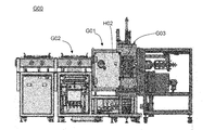
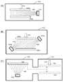
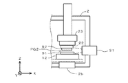
- FIG. 1 is an external view of a substrate bonding system G00 including a load lock device G02, a bonded substrate manufacturing device G01, and a substrate bonding device G03.
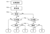
- 2 is a flowchart showing a plurality of types of processes (bonded substrate manufacturing method) for forming a bonding surface on a substrate, in which a silicon thin film is formed in the bonding surface layer according to different embodiments of the present invention.
- Process bonded substrate manufacturing method).
- A is a schematic diagram showing a relevant part for performing the irradiation step (surface treatments F03, F05) of FIG.
- FIG. 1 It is a schematic diagram which shows the relevant part for implementing the silicon thin film formation process (process F04) of FIG. 2 among the board
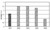
- 3 is a graph showing the bonding strength of the bonding substrate AE obtained by each process AE of FIG.
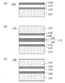
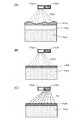
- (A) is a schematic diagram showing a cross-sectional structure of the bonding substrate E obtained from the process E of FIG. 2 based on the embodiment
- (B) is a bonding of the bonding substrates E to each other based on the embodiment.
- It is a schematic diagram which shows the cross-sectional structure of the obtained board
- (C) The schematic diagram which shows the cross-sectional concept of the board
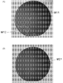
- (A) is an infrared transmission image showing the formation of the void M12 of the substrate assembly A obtained from the process A in FIG. 2
- (B) is the substrate assembly E obtained from the process A in FIG. It is an infrared transmission image in which void formation is not recognized.
- FIG. 4 is a transmission electron micrograph showing a fine structure of a cross section in the vicinity of a bonding interface of a substrate bonded body E. It is an EELS scan by transmission electron microscopy showing the concentration distribution of iron in the direction perpendicular to the bonding interface at and near the interface layer of the substrate bonded body E. It is a graph which shows the joint strength in each condition (N04 and N05) of the combination of board
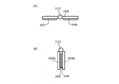
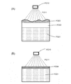
- (A) is a front view schematically showing positions 1 to 5 for measuring the etching amount on the substrate H06 by the particle beam H05 emitted from the particle beam source H03 according to the embodiment of the present invention.
- FIG. 14 is a cross-sectional view of the line particle beam source H03 of FIG. 13 taken along the line P1P2P3.
- the diagram which shows the relationship between memory SS01 which stored the look-up table, control apparatus SS02, particle beam source FG20, and particle source FG30. It is a diagram which shows the relationship between computer S01, power supply S02 which applies an acceleration voltage based on the instruction
- V acceleration voltage
- (A) is a process of radiating energetic particles from one particle beam source FG10 to remove the oxide film FG02 and the impurities FG03 on the surface of the substrate FG01, and (B) is a bonding layer FG04 on the substrate FG01. It is a schematic diagram which shows the process in which is formed.
- FIG. 4 is a schematic diagram showing a process of forming a final bonding layer FG04 by radiating metal particles FG31 onto a substrate FG01.
- FIG. 1 It is a schematic diagram which shows the specific example of an energetic particle source. It is a schematic diagram which shows the specific example in case an energetic particle source has a horn-shaped metal body further. It is a graph which shows the specific example of the relationship between the acceleration voltage of energetic particle, and joining strength. It is the iron 2p spectrum of the board
- “Substrate” is synonymous with “solid material”, and the substrate may have any shape. In the preferred embodiment described below, the substrate may take the form of a wafer. However, this is for illustrative purposes only and is not intended to be limiting.
- “Energetic particles” can be inert gas ions and / or neutral atoms.
- Metal particles can be metal ions, metal neutral atoms and / or clusters.
- An energetic particle source is a device that emits energetic particles. “Emit” is synonymous with “release”. “Energetic radiating particles” or “radiant energy particles” are particles emitted or emitted from an energetic particle source.
- a “metal particle source” is a device that emits and emits metal particles.
- the metal body emits and releases metal particles in response to energetic particle radiation.
- a combination of an energy particle source that emits energy particles to the metal body and the metal body constitutes the metal particle source.
- This type of metal particle source is called a sputter metal particle source.
- FIG. 1 shows the appearance of the substrate bonding system G00.
- the system G00 typically includes a load lock device G02, a bonded substrate manufacturing device G01, and a substrate bonding device G03. It should be noted that the appearance itself of the system G00 or the details of the appearance does not constitute a part of the present invention.
- the load lock device G02 is a substrate carry-in and carry-out port for the bonded substrate or the bonded substrate assembly.
- the bonded substrate manufacturing apparatus G01 performs a process (bonded substrate manufacturing method) in which a bonded surface is formed on a carried-in substrate and a bonded substrate is manufactured. In general, this process requires a high vacuum environment. For this reason, the bonding substrate manufacturing apparatus G01 performs the process in a state where the inside of the process chamber H02 is in a high vacuum (for example, the atmospheric pressure is 10 ⁇ 7 Pa). Usually, before the substrate is introduced into the process chamber H02, a pressure reducing operation is performed to lower the inside of the load lock device G02 loaded with the substrate from the atmosphere to a predetermined vacuum.
- the substrate bonding apparatus G03 is for bonding bonded substrates to produce a substrate bonded body.
- the substrate bonding apparatus G03 is connected to the bonding substrate manufacturing apparatus G01, and the bonding substrate is supplied from the bonding substrate manufacturing apparatus G01 in a state where the atmosphere is in communication.
- the manufactured substrate bonded body can be transferred to the load lock device G02 which is a carry-out port via the bonded substrate manufacturing device G01.
- a robot (not shown) transfers processing devices such as a substrate, a bonded substrate, and a substrate bonded body.
- the substrate bonding apparatus G03 uses a vacuum atmosphere as a process requirement, and bonding (bonding) between bonded substrates is performed under a predetermined vacuum. As will be described later, according to one aspect of the present invention, the substrate bonding apparatus G03 does not require a vacuum atmosphere. In a preferred embodiment of the present invention, the bonding substrate manufactured by the bonding substrate manufacturing apparatus G01 does not require bonding in a vacuum atmosphere. Therefore, in the embodiment of the present invention, the substrate bonding apparatus G03 may be an independent apparatus separated from the bonded substrate manufacturing apparatus G01.
- the bonded substrate manufacturing apparatus G01 forms a bonded substrate by forming a bonded surface on a given substrate.
- some embodiments will be described with respect to a bonding substrate manufacturing method performed by the bonding substrate manufacturing apparatus G01 and related portions of the bonding substrate manufacturing apparatus involved in the implementation of the method.
- FIG. 2 is a flowchart showing a plurality of types of processes (bonding substrate manufacturing method) for manufacturing a silicon thin film embedded bonding surface on a substrate based on different embodiments of the present invention. These processes are performed by the bonding substrate manufacturing apparatus G01. First, a starting substrate is obtained in the first step (F01), and then preprocessing (F02) is performed to obtain a substrate on which a bonding surface is to be formed.
- preprocessing F02
- a commercial industrial silicon substrate having a diameter of 150 mm was used as the starting substrate.
- an oxide film was formed on the surface of the silicon substrate by a general thermal oxidation method.
- a bonded substrate manufacturing process for forming a silicon thin film embedded bonding surface on the substrate is performed after the pretreatment F02 according to a different embodiment of the present invention.
- processes that can be selected five processes A to E are shown in FIG.
- Process A is a process (bonded substrate manufacturing method) in which only the surface treatment (“irradiation” step F03) is performed on the substrate surface. Unlike the other processes BE, the silicon thin film is not formed (F04) on the bonding surface. A substrate manufactured by this process is referred to as a bonded substrate A. Therefore, process A is a comparative reference process and substrate A is a comparative reference substrate.
- Process E is a process in which after the surface treatment (F03) is performed on the substrate surface, a silicon thin film is formed on the surface-treated substrate surface (F04), and the surface of the formed silicon thin film is further surface treated (F05). .
- a substrate manufactured by this process is referred to as a substrate E.
- the surface of the silicon oxide film L01 is surface-treated (L02) and the silicon thin film (L03) is formed on the surface of the bonding substrate E (L00).
- This is a (L04) substrate on which a silicon thin film has been surface-treated.
- Process C is the same as process E up to the surface treatment F03 on the substrate surface and the silicon thin film formation F04, but the final silicon thin film surface treatment F05 is not performed.
- This is referred to as a bonded substrate C obtained as a result.
- the bonding substrate C is a substrate in which a silicon oxide film surface is surface-treated and a silicon thin film is formed on the surface.
- Process D is a process in which a silicon thin film is directly formed (F04) without performing the surface treatment F03 on the substrate surface, and the surface of the formed silicon thin film is surface treated (F05).
- the substrate thus manufactured is called a bonded substrate D.
- the bonding substrate D is a substrate in which a silicon thin film is formed on the surface of the silicon oxide film without being subjected to surface treatment, and is further surface-treated.
- Process B is a process in which a silicon thin film is formed directly on the substrate surface (F04).
- the substrate thus obtained is called a bonded substrate B.
- the bonding strengths of the bonding substrates B to E according to the embodiment showed an unexpected difference with respect to the comparative reference substrate A.
- the surface treatment F03 on the substrate surface may be referred to as “step 1”
- the silicon thin film formation treatment F04 may be referred to as “step 2”
- the surface treatment F05 on the silicon thin film surface may be referred to as “step 3”.
- FIG. 3 schematically shows a relevant part suitable for carrying out Steps 1 and 3 and Step 2 (surface treatment and silicon thin film formation treatment) of FIG. 2 in the bonding substrate manufacturing apparatus G01 together with the process chamber H02. It is shown in. Basically, for surface treatment, a particle source (see H03) that emits energetic particles on the substrate is required.
- the formation of the silicon thin film can be realized by a CVD method using a CVD apparatus, a PVD method using a PVD apparatus, or the like as a silicon source.
- FIG. 3 shows a sputter type silicon source (see H10).
- the process chamber H02 has an atmospheric pressure of 10 ⁇ 7 Pa as a degree of vacuum before the start of the process.
- the substrate H06 is supported by the substrate support H08.
- the energetic particle source H03 is provided so that the substrate H06 can be irradiated with radiation particles H05 including energetic particles and metal particles.
- the energetic particle source H03 has a rotation axis H04 in a direction perpendicular to the drawing, and the attitude of the energy particle source H03 can be controlled around the rotation axis H04. This constitutes a simple attitude control device. If desired, an attitude control device that controls the attitude of the energetic particle source H03 for a plurality of axes can be used.
- the bonding substrate manufacturing apparatus includes an energy particle source H03 that emits radiation particles including energy particles, a silicon source H10, and an attitude control device H04 that controls the attitude of the energy particle source H03.
- the attitude control device H04 causes the energetic particle source H03 to take the first attitude in the surface treatment mode according to steps 1 and 3, and directs the emitted particles from the energetic particle source H03 toward the surface of the substrate H06.
- the energetic particle source takes the second posture, and the radiating particles from the energetic particle source H03 are directed to the silicon source H10.
- the substrate H06 in response to the emitted particles from the energetic particle source H03. Is placed in position to emit silicon particles toward the surface, it is understood.
- the substrate support H08 can support a plurality of substrates in addition to the substrate H06.
- the substrate H07 is further supported.
- the substrate support H08 includes a mechanism H09 that moves in the lateral direction in FIG. 3A, and the substrate support H08 is translated with respect to the energy particle source H03 by the moving mechanism H09.
- the substrates H06 and H07 can be sequentially irradiated with the radiation particles.
- the substrate H06 can be moved out of the irradiation range of the radiating particles H05. It is possible to avoid irradiating the substrate H06 with unfavorable conditions such as instability immediately after ignition of the energetic particle source H03.
- the other substrates H07 held by the substrate support H08 can be irradiated with the radiating particles H05 sequentially or continuously. By doing so, the speed and efficiency of the entire process can be improved.
- a line-type particle source (line-type ion source) that is long in the position direction as shown in FIG. 13 is used, and a substrate having a large size is arranged by arranging it in the direction perpendicular to the paper surface in FIG. It is also possible to process efficiently.
- the energetic particle source H03 can emit radiation particles including energetic particles.
- the energetic particles may be inert particles and preferably contain argon.
- the energetic particle source H03 can further emit radiation particles including metal particles.
- This metal particle is preferably a transition metal, more preferably iron.
- the particle source H03 that emits both energetic particles and metal particles can take several configurations.
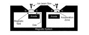
- this type of particle source H03 which emits both energetic particles and metal particles, generates a plasma of inert particles (argon) and applies an electric field E to the plasma to produce plasma inert particles. Is accelerated in the direction of the electric field to generate radiation of energetic particles including inert particles.
- the particle source H03 by disposing a metal body that can move freely including a desired metal in a region where a plasma of inert particles (argon) is generated, the metal particles are moved from the metal body by the energy particles derived from the plasma. Released and becomes part of the emitted particle.
- the particle source of this configuration functions as a particle source that mainly emits energetic particles when the metal body is in the retreat position by selecting the operation mode, and when the metal body is in the advanced position (position in the plasma space). Functions as a particle source that emits metal particles together with energetic particles.
- the ratio of the metal particles contained in the total radiation particles or the amount with respect to the energetic particles can be enhanced or controlled by various methods.
- a metal that is emitted from the particle source by further providing a cone-shaped metal body at the outlet of the particle source H03 and sputtering the metal body with energetic particles (in this case, inert particles in a plasma state).
- energetic particles in this case, inert particles in a plasma state.
- the amount of particles can be increased.
- a grid-like metal body is further provided at the outlet of the particle source H03, and energetic particles (in this case, inert particles in a plasma state) sputter the metal grid, thereby reducing the discharge amount of the metal particles. Can be increased.
- the ratio of metal particles contained in the total radiation particles or the amount with respect to energetic particles is not limited to the above configuration example.
- the metal body that generates the metal particles may be located at a position remote from the particle source and between the particle source and the substrate to be irradiated and exposed to particle radiation including energetic particles.
- position in arbitrary positions.
- the shape of the metal body may be any shape in order to achieve the same purpose.
- FIG. 3B shows a structure in which the process chamber H02 shown in FIG. 3A further includes a silicon source H10.
- the silicon source H10 is arranged so that the silicon H11 can be emitted in the direction of the substrate H06 on which the silicon is deposited, and further receives radiation particles H05 from the particle ion beam H03 to emit silicon. Arranged to be able to.
- the particle ion beam H03 rotates around the rotation axis H04 from the position shown in FIG. 3A and is emitted in the direction of the silicon source H10.
- the energetic particle source H03 and the silicon source H10 are arranged with respect to the substrate H06 in the process chamber H02, so that one energetic particle source H03 is formed. It is possible to perform irradiation with radiation particles on the substrate H06 and sputter deposition of a silicon thin film on the substrate H06. By doing so, the structure of the components in the process chamber H02 can be simplified.
- the substrate bonding apparatus G03 is for bonding bonded substrates to each other.
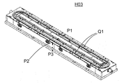
- the substrate bonding mechanism G03 is not limited, but for example, a mechanism that functions as shown in FIG. 5 is preferable. That is, the substrate support portion H08 includes a support portion H08a and a support portion H08b that support the substrate H06 and the substrate H07, respectively.
- the support portion H08a and the support portion H08b can rotate about a rotation axis H12 in a direction perpendicular to the paper surface of FIG. 5 to bring the bonding surfaces of the substrate H06 and the substrate H07 into surface contact with each other.
- the substrates can be bonded together in a desired time and condition in the process chamber H02 or in another vacuum chamber (not shown) without taking out the substrate from the bonding surface manufacturing apparatus G00. Enable.
- the pair of substrates A to E related to the same process is illustrated in the substrate bonded device G03.
- bonding was performed as shown in FIG.
- the pair of bonded substrates will be referred to as substrate bonded bodies A to E.
- the structure of the substrate assembly E is shown in FIG.
- the substrate E is irradiated with the surface of the silicon oxide film L01 in step 1 (L02), a silicon thin film (L03) is formed on the surface, and the silicon thin film is irradiated in step 1 (L04). ing.
- the surfaces L04 are bonded to each other to form a substrate bonded body E (L10).
- FIG. 4 shows an average value obtained by a plurality of measurements for each of the substrate assemblies A to E.
- the substrate bonded body A obtained by bonding the substrates irradiated with the silicon oxide film in the step 1 without forming the silicon film showed the lowest bonding strength (0.05 J / m 2 or less).
- the substrate joined body B obtained by joining the substrates on which the silicon films were formed without any step 1 showed a joining strength (0.37 J / m 2 ), which was higher than that of the substrate joined body A. .
- the substrate bonded body D obtained by bonding the substrates that have passed through the step 1 shows a bonding strength (0.51 J / m 2 ). High bonding strength was shown. This is a bonding strength of about 20% of the fracture strength (2.5 J / m 2 ) of the bulk material of silicon.
- the substrate joined body C in which the substrates are joined without going through the step 1 shows the joining strength (1.17 J / m 2 ), and the substrate joined body D Even higher bonding strength was exhibited. This is a bonding strength of about 40% of the fracture strength (2.5 J / m 2 ) of the bulk material of silicon.
- the substrate joined body E in which the substrates passed through the step 1 were further bonded showed the highest bonding strength (1.55 J / m 2 ). This is a bonding strength of about 60% of the fracture strength (2.5 J / m 2 ) of the bulk material of silicon.
- the results of the bonding strength shown in FIG. 4 indicate that the substrate on which the silicon film is formed clearly shows higher bonding strength than the substrate on which the silicon film is not formed, and step 1 is performed before and after the formation of the silicon film. It shows that the bonding strength increases.
- a pair of substrates subjected to the same type of processing are bonded to each other, and the bonding strength of the substrate bonded body between the processing methods is compared. Even when one substrate is processed, the same effect is obtained. It is clear to play.
- silicon oxide is used as the substrate (surface layer portion), but it is obvious that the present invention is not limited to this.
- a silicon thin film in the bonding surface layer a wide range of application is recognized in that there is no restriction in principle on the material of the substrate itself.
- the present invention can be applied to any substrate material as long as irradiation of the substrate surface with energetic particles and generation of a silicon thin film are possible.
- voids indicates that there are voids between the substrates due to the presence of unwanted particles adhering to the bonding surface at the bonding interface, and the bonding strength is weak.
- FIG. 7A shows an infrared transmission image of the substrate assembly A (M11), and FIG. 7B shows an infrared transmission image of the substrate assembly E (M21).
- FIG. 7A it was confirmed that a void was formed at a position indicated by M12. on the other hand.
- FIG. 7B formation of voids as indicated by M12 in FIG. 7A could not be recognized.
- the substrate E has a larger number of processes than the substrate A, and therefore, it is considered that there is a high probability that unwanted particles and the like adhere to the bonding surface before bonding.
- the fact that no void was formed in the substrate assembly E suggests that the bonding strength of the substrate assembly E is significantly higher than that of the substrate assembly A, and the bonding strength shown in FIG. Consistent with the results.
- FIG. 8 shows a fine structure obtained by transmission electron microscopy in the vicinity of the bonding interface of the substrate assembly E.
- the substrate E is formed by forming the surface of the silicon oxide film L01 on the silicon substrate (L10) as a starting material, and irradiating it in step 1 (L02), and forming a silicon thin film (L03) on the surface.
- the surfaces L04 are bonded to each other to form a substrate bonded body E (L10).
- FIG. 9 shows a concentration profile in the direction perpendicular to the iron joining interface measured by line scanning in the direction perpendicular to the joining interface L04 (K31).
- iron was present at the locations L02 and L04 irradiated with energetic particles in Step 1 and was not measured at other locations. Furthermore, the iron concentration at the bonding interface L04 is higher than that in the portion L02 irradiated with energetic particles before the silicon thin film L03 is deposited. This is considered to correspond to the fact that iron is contained approximately twice as much as the surfaces irradiated with energetic particles under the same conditions in step 1 are combined.
- FIG. 6C will be described.
- the surface of one substrate L01 is irradiated in step 1 (L02), a silicon thin film (L03) is formed on the surface, and the silicon thin film is irradiated in step 1 (L04), and then bonded to another substrate L41.
- L02 silicon thin film
- L04 silicon thin film
- the metal contained in the other energy particles is present at a higher concentration than the other locations.
- This metal is preferably a transition metal, more preferably iron.
- step 1 is performed at an acceleration voltage of 1.5 to 2.5 kV and a current of 350 to 400 mA
- step 2 is performed at an acceleration voltage of 1.0 to 1.0.
- the operation was performed at 2.0 kV and a current of 300 to 500 mA.
- the bonding substrate manufacturing method (see FIG. 2) of the type for forming the “silicon thin film layer” in the bonding surface layer, the bonding substrate (FIG. 6) and the substrate bonded body (FIG. 6) as the apparatus and the product are described. did. As shown in FIG. 4, it has been found that forming a silicon thin film in the bonding surface layer provides a high bonding capability for the bonding substrate as compared to the case without it. In addition, the present method and apparatus have no limitation on the material of the substrate that can be applied, and are very effective.
- bonded substrate manufacturing method for manufacturing a substrate on which a bonded surface is formed (“bonded substrate”).
- a first surface treatment step of irradiating the surface of the substrate with radiation particles including energetic particles to perform surface treatment, and a second surface treatment of the substrate surface by irradiation with radiation particles including metal particles are performed.
- the bonded substrate is manufactured, and the execution of each step is controlled so that the metal particles are distributed in the base material of the surface layer of the bonded substrate.
- the first surface treatment step and the second surface treatment step can be performed simultaneously.
- the energetic particle source / metal particle source H03 already described in FIG. 3 has been described.
- a sequential process can be used in which energetic particle radiation is applied to the substrate surface and then metal particle radiation is applied to the substrate surface.
- the use of an energetic particle source / metal particle source H03 or the operation of a metal particle source followed by the operation of the energetic particle source can be used.
- a bonded substrate manufacturing apparatus G01 for forming a bonded surface of a substrate an energy particle source FG20 that irradiates the surface of the substrate with radiation particles containing energy particles, and the surface of the substrate
- a process condition memory SS01 that stores process conditions that satisfy a target bonded substrate property (“target property”)
- target property a target property
- the target property includes that metal particles are distributed in the base material of the surface layer of the bonded substrate, and the energy particle source FG20 and the metal particle source FG30 are controlled by the control device SS02. Operation is controlled based on process conditions that satisfy the target property.
- the target properties may include (A) the absence of a metal layer in the surface layer of the bonded substrate and (B) the distribution of metal particles in the matrix of the surface layer of the bonded substrate, and the energetic particle source FG20.
- the operation of the metal particle source FG30 is controlled based on a process condition that satisfies the target property under the control of the control device SS02.
- the process condition may include an energy condition acquired by the energy particles by the energy particle source FG20.
- the energy condition may be 30 eV or more.
- the target property includes “the bonding substrate has a predetermined bonding strength capability”, and the energy particle source FG20 and the metal particle source FG30 are controlled by the control device SS02. Operation is controlled based on process conditions that satisfy the target property. For example, look-up tables T01 and T02 as shown in FIG. 20 may be prepared in the process condition memory SS01 so that the bonding strength (for example, expressed by the substrate breakdown strength ratio) can be presented.
- control unit S01 shown in PC format has a built-in memory that stores process requirements relating to energy requirements, and the voltage corresponding to the required acceleration energy is supplied to the power source S02. An instruction is given via the data bus S03. In response to this, the energetic particle source H03 is operated to a voltage corresponding to the acceleration energy requested from the power supply S02 via the power supply line S04.
- Surface treatment is a process of irradiating the substrate surface with energetic radiation particles.
- Oxides are often formed when the substrate material reacts with atmospheric oxygen or water during a wet process.
- silicon which are mostly SiO 2.
- impurities There are various forms and types, and in this specification, they are simply referred to as “impurities”.
- surface treatment is to firstly remove the oxides and impurities by collision of radiation particles including energetic particles, thereby exposing the clean surface of the substrate material itself.
- the surface of the substrate material itself is in an unstable state with high energy due to the presence of dangling bonds, avoiding oxidation and adhesion of impurities, and contacting with other clean surfaces that are unstable in energy, As dangling bonds are bonded to each other and stabilized in energy, a strong bond can be obtained.
- the second purpose of “surface treatment” is to further irradiate the clean surface with radiation particles containing energetic particles, thereby disturbing the crystallinity of the substrate material and promoting the formation of dangling bonds. Get higher. Therefore, a stronger bond can be obtained by bonding the surfaces.
- an inert gas particularly argon
- argon is used for the radiating particles including energetic particles used in the “surface treatment”.
- the present invention is not limited to this.
- other inert gas may be used, and even if it is not an inert gas, particles such as nitrogen molecules, oxygen molecules, etc. that transmit kinetic energy obtained by acceleration to the particle source to the substrate material. Any type is acceptable. In addition to kinetic energy, it may be chemically reactive with the substrate material.
- the particles used in the “surface treatment” particle emission may include a plurality of types of particles.
- metal particles may be included.
- the metal particles that have reached the surface of the substrate material are considered to undergo some kind of chemical reaction during bonding, and as a result, the bonding strength is further increased.
- “Surface treatment” may be performed on both surfaces of a pair of substrates to be bonded or on one surface.
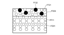
- the surface treatment method based on this embodiment the case where silicon is used as the substrate material, the energy particles are argon, and the metal is iron atoms will be described with reference to FIG. That is, in the substrate FG01, the silicon atoms FF11 are arranged in a diamond crystal structure.
- the surface treatment method based on this embodiment it is considered that the diamond crystal structure is lost in the silicon substrate surface layer FG04, and the silicon atoms FF21 form the amorphous layer FG04.
- the iron atom FF22 is considered to exist mainly in the amorphous layer FG04.
- FIG. 25 shows the composition analysis result in the depth direction of the silicon substrate after irradiation with energetic particles and iron particles by high frequency glow discharge emission analysis. This result indicates that there is an iron concentration peak in the surface layer, and the peak concentration is 4.5 atomic% (hereinafter referred to as “atomic%”).
- Iron atoms other than the amorphous layer FG04 may exist in the substrate FG01. This is because the diffusion coefficient of transition metals in semiconductor materials is generally high, for example, the diffusion coefficient of iron in silicon is very high (Sze, Physics of Semiconductor Devices). Therefore, even at room temperature, the diffusion coefficient of transition metals typified by iron is high. Even if the temperature of the entire substrate is kept at room temperature or a temperature lower than room temperature, the energy of the energy particles is converted into thermal energy by collision during irradiation with energetic particles, and the temperature near the surface is It is said to rise locally within the range of the primitive level. Therefore, the iron diffusion distance is considered to increase near the surface. However, it is iron atoms located in the vicinity of the substrate surface that participate in the bonding process, while iron atoms that are deeper than the amorphous layer FG04 when viewed from the surface do not directly participate in the bonding process.
- the acceleration energy of iron atoms may be lower than the acceleration energy of argon, which is an energetic particle. Since the diffusion rate of iron atoms is higher in amorphous silicon than in crystalline silicon, sufficient diffusion of iron atoms can be considered.
- the surface layer FG04 generated by the surface treatment method according to this embodiment preferably contains 0.1 to 30 atomic% of metal.
- the surface layer FG04 generated by the surface treatment method according to the present embodiment contains 3 to 10 atomic% of metal.
- the metal content is larger than a predetermined amount.
- the metal content is greater than a predetermined amount, sufficient bonding strength may not be obtained.
- a substrate having an iron content of 5 atomic% in the surface layer FG04 is bonded after the pressure is changed from vacuum to atmospheric pressure, a high bonding strength is obtained.
- the substrate with the iron content of 5 atomic% in the surface layer FG04 has a lower oxidation rate than the case of the iron metal film.
- iron atoms can be considered to be isolated from other iron atoms.
- iron atoms combine with silicon atoms to form a silicon alloy.
- a silicon alloy is considered to be less likely to be oxidized than when a metal film is formed adjacent to iron.
- iron atoms are present in the surface layer FG04, one end of the iron atom is bonded to the silicon atom, but the other end is exposed on the surface and is not bonded to the silicon atom or the like. have.
- the iron atom on the outermost surface after this surface treatment has a property that it does not easily oxidize because the content does not exceed a predetermined amount, but it has a sufficient strength when it comes into contact with other substrate surfaces. It can be considered to have activity as much as it occurs.
- metal atoms when the metal content in the surface layer FG04 increases, metal atoms continue to form a metal bond.
- the continuous metal bonding in the surface layer FG04 makes the layer conductive. Even if it is not completely continuous, if a metal atom is present in the vicinity at the atomic level, conductivity may occur due to the tunnel effect. Alternatively, even when the surface layer FG04 alone does not have conductivity, conductivity may be generated by joining a similar pair of surface layers FG04.
- energetic particles and metal particles are radiated from the particle source, so that the driving conditions of the particle source define the energy of the energy particles and metal particles.
- the energy particles and the metal particles play different roles in the action on the substrate material. If the amount of the metal particles reaching the surface of the substrate material exceeds the amount of the energy particles removed from the substrate material, the metal particles will be deposited on the surface of the substrate material. In this case, a metal film is formed. On the other hand, if the amount of the metal particles reaching the surface of the substrate material is smaller than the amount of the energy particles removed from the substrate material, the metal particles are not deposited on the surface of the substrate material and the removal of the substrate material proceeds. That is, the balance between the kinetic energy of energetic particles and the amount of metal particles reaching the substrate material surface is an element for forming a desired thin film.
- FIG. 11A is a side view showing a positional relationship among the irradiation direction of the substrate H06, the energetic particle source H03, and the energetic particles H05.
- FIG. 11B is a plan view thereof.
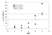
- the substrate H06 a thermal oxide film was formed on a silicon substrate, the thickness of the thermal oxide film was measured before and after irradiation with energetic particles, and the difference in thickness was defined as the etching amount.
- the energetic particle source H03 was irradiated with energetic particles H05 so as to include the center 3 of the substrate from an oblique direction with respect to the substrate surface.
- the thickness of the thermal oxide film was measured along points 1 to 5 in the diameter direction on the substrate H06, that is, along the irradiation direction O01 of the energetic particles H05.
- the measurement points 1 to 5 were positioned by positioning the notch O02.
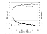
- FIG. 12 shows etching amounts (nm) at 80 V and 100 V at the respective measurement points 1 to 5.
- the etching amount was measured under two conditions of irradiation doses of 15 and 30 Amin, and it was confirmed that the etching amount was almost proportional to the irradiation amount.
- 100 V almost the same results were measured for the etching amounts at 80 V and 30 Amin at the measurement points 1 to 3, and at the positions 4 and 5, the intermediate etching amount between the results of the above two conditions of 80 V was measured. In either case, it was found that the irradiation with energetic particles at 80V and 100V gives almost the same etching amount of the thermal oxide film.
- the silicon substrate was surface-treated with the same energy particle acceleration voltage and bonded. At this time, an oxide film and other thin films other than silicon were not formed on the surface of the silicon substrate, and the silicon materials were bonded to each other.
- an acceleration voltage of 80 V sufficient bonding strength cannot be obtained.
- energetic particles are accelerated and surface-treated at an acceleration voltage of 100 V, sufficient bonding strength is obtained. It was. This measurement result shows that the bonding strength varies depending on the acceleration voltage in a certain particle source, that is, the kinetic energy of the energetic particles, even under energetic particle irradiation conditions that give an equivalent etching amount.
- the acceleration voltage 80V and 100V of energetic particles using a predetermined particle source may vary depending on various conditions.
- the acceleration voltage may be 30 V (see FIG. 31).
- the kinetic energy of energetic particles depends on the configuration of the particle source used.
- silicon was used in the above embodiment, the bonding strength is not only kinetic energy (particle energy) but also the type of material irradiated with energetic particles (semiconductor, ceramic, dielectric material, organic material, etc.) ) And morphology (single crystal material, crystal orientation on material surface, polycrystal, crystal grain size, etc.). Therefore, it can be said that the obtained bonding strength depends on parameters such as the energy of particles, the material to be irradiated, and the particle source.
- the computer S01 issues an instruction S03 regarding the value of the required acceleration voltage to the power source S02. Output to.
- the power source S02 applies the instruction voltage to the electrode plate S05 of the acceleration voltage of the energetic particle source H03 according to the instruction.
- the particles H05 accelerated at the predetermined voltage are emitted from the energetic particle source H03.
- the energy particles include metal particles.
- FIG. 21 the difference between the above embodiment (FIGS. 21A and 21B) and the present embodiment (FIGS. 22A to 22C) will be described.
- energetic particles are emitted from one particle source FG10 to remove the oxide film FG02 and the impurity FG03 (FIG. 21A) on the surface of the substrate FG01, and the bonding layer FG04 is formed on the substrate FG01. It is formed (FIG. 21B).
- the energy particles include metal particles
- the formed bonding layer FG04 includes this metal.
- the final bonding layer FG04 is formed by radiating the metal particles FG31 onto the substrate FG01 using the particle source FG30 having a different radiation amount of the metal particles (FIG. 22C).
- the energy particles in the first step may or may not contain metal particles.
- the particle source FG30 in the second step may be one that emits energetic particles and metal particles at the same time as used in the above embodiment. It is conceivable that the radiation amount of the metal particles is increased or decreased by various methods. Further, the particle source FG30 may not include a mechanism for accelerating the particles. In short, according to the embodiment exemplified in the present embodiment, the irradiation conditions of the energetic particles and the irradiation conditions of the metal particles are set relatively freely in the first step and the second step, and each operation is better controlled. It becomes possible to do.
- the energetic particle source does not radiate energetic particles toward the substrate H06 but radiates toward the metal particle source FG30.
- the metal particle source FG30 reacts with the energetic particles FG21 to sputter the metal particles FG31 and radiates it toward the substrate H06.
- the metal particle source FG30 is a sputter target for the energetic particles FG21.
- a sputter target in which metal particles and silicon are sputtered by switching appropriately according to the process is effective.
- the sputter target has a polygonal prism shape having a plurality of surfaces and is rotatable, and a silicon target is provided on at least one surface, and a metal particle target is provided on at least one other surface.
- energy particles are emitted to the silicon target to sputter silicon to form a silicon film on the substrate, and then the rotary sputter target is rotated. It becomes easy to radiate energetic particles to the metal particle target to sputter metal particles (for example, iron particles) and irradiate the metal particles on the substrate.
- the substrate (surface layer portion) material was silicon oxide. That is, although the material of the starting substrate is silicon, the surface is thermally oxidized to form silicon oxide, and the substrate is an embodiment as silicon oxide because of the configuration of the present invention.
- a material other than silicon oxide was used as the substrate in the following specific example in which no silicon thin film was inserted into the bonding surface.
- both substrates were bonded after being subjected to the same process as the bonding surface preparation process of the substrate E shown in FIG. Therefore, the structure of the interface of the substrate bonded body is the same as that of the substrate bonded body E described above.
- the bonding strength of the substrate bonded body was measured by the blade insertion method, which is the same as the measurement of the bonding strength in FIG.
- a silicon substrate is used as one substrate, a bonding surface is prepared without performing a process such as thermal oxidation, and a silicon substrate is used as another substrate. After forming silicon nitride, a bonding surface was prepared. Therefore, the present embodiment substantially shows the measurement results of bonding surface preparation, bonding, and bonding strength between silicon and silicon nitride.
- the bonding strength of this example was estimated to be 2.5 J / m 2 .
- the substrate did not peel and the silicon substrate was destroyed, so the actual bonding strength of this example was measured.
- the destruction of the silicon substrate indicates that a high-strength bonding surface was formed. That is, the bonding strength in this embodiment has at least the breaking strength of the bulk material of silicon.
- the bonding strength at this time was estimated from the lower limit value and described as a bulk fracture strength of silicon of 2.5 J / m 2 .
- the strength of the substrate bonded body N02 in this example was higher than that of the substrate bonded body E (N01 in FIG. 10), and at least the bonding strength of the silicon substrate bonded body.
- a silicon substrate is used as one substrate, the surface of the silicon substrate is thermally oxidized, a bonding surface is prepared, and a silicon substrate is used as the other substrate. After forming the silicon nitride, the bonding surface was prepared. Therefore, the present embodiment substantially shows the results of measurement of bonding surface preparation, bonding, and bonding strength between silicon oxide and silicon nitride.
- the bonding strength of this example was estimated to be 2.5 J / m 2 . Similar to N02, when the blade was inserted, the substrate was not peeled off and the silicon substrate was broken. Therefore, 2.5 J / m 2 , which is the bonding interface strength of the silicon material, was described as an estimated value.
- the strength of the substrate bonded body N03 in this example was higher than that of the substrate bonded body E (N01 in FIG. 10), and at least the bonding strength of the silicon substrate bonded body.
- a silicon substrate was used as both substrates, and after forming silicon nitride on the surface of any silicon substrate, a bonding surface was prepared. Therefore, the present embodiment substantially shows the results of measurement of bonding surface preparation, bonding, and bonding strength between silicon nitride and silicon nitride.
- the bonding strength of this example was measured to be 2.25 J / m 2 .
- the silicon substrate was not destroyed. This is a bonding strength of about 90% of the fracture strength (2.5 J / m 2 ) of the bulk material of silicon.
- the measurement of the actual bonding strength revealed that the strength of the substrate bonded body N04 in this example was higher than that of the substrate bonded body E (N01 in FIG. 10).
- the measurement results of the bonding strengths of the substrate assemblies N02, N03, and N04 in the above examples are all higher than those of the substrate assembly N01. This indicates that the method according to the present invention can obtain high bonding strength without depending on the type of the substrate.
- the substrates were bonded in a vacuum after being subjected to the bonding surface preparation process according to the present invention.
- the substrate was bonded in an atmosphere of atmospheric pressure after the same process for forming the bonding surface as in the above-described silicon nitride-silicon nitride example (N04 in FIG. 10).
- the bonding strength of the substrate bonded body N05 produced by bonding in an atmospheric pressure atmosphere was 0.9 J / m 2 as shown in the rightmost part of FIG. This is a bonding strength of about 35% of the fracture strength (2.5 J / m 2 ) of the bulk material of silicon.
- the bonding strength of the substrate assembly N05 is lower than the bonding strength of the substrate assembly N04, but is higher than the bonding strength of the substrate assembly A or B shown in FIG. Therefore, by using the method according to the present invention from the measurement result of the bonding strength, a sufficiently high bonding strength can be obtained even when the atmospheric pressure during bonding is atmospheric pressure. Furthermore, it is naturally predicted that the bonding strength when the atmospheric pressure during bonding is lower than the atmospheric pressure is higher than that of the substrate bonded body N05.
- FIG. 1 An example of the device configuration is shown in FIG.
- a pair of substrates H06a and H06b are disposed with their bonding surfaces facing each other in a process chamber H02 that can be in a vacuum atmosphere.
- the energetic particle source H03 emits energetic particles H05 in the horizontal direction to the surfaces of the substrates H06a and H06b and toward the space between both substrate bonding surfaces, whereby both the bonding surfaces of the substrates H06a and H06b are Surface treatment at the same time.
- a bonding mechanism H13 is further provided so that both substrates can be brought into contact with each other after the surface treatment.
- One energetic particle source H03 can perform surface treatment on a pair of substrates, and since the distance between the substrates is small, the apparatus configuration is simple and economical. In addition, since the bonding can be performed immediately after the surface treatment, the chance of reattachment of impurities after the surface treatment can be reduced.
- FIG. 15A Another embodiment of the apparatus configuration is shown in FIG.
- the apparatus configuration shown in FIG. 15A since the substrate surface is substantially parallel to the direction of the energy particles H05, the difference in the intensity distribution of the energy particles on the substrate surface is large, and hence the energy particle irradiation on the substrate surface is uniform. It's hard to say. Further, since the distance between the substrates is small, there is a problem that impurities removed from the surface of one substrate adhere to the surface of another substrate. Therefore, in the apparatus configuration shown in FIG. 15B, the energy particle source H03 is provided for each of the substrates H06a and H06b, the substrate interval is widened, and the energy particles H05 are irradiated at a larger angle with respect to the substrate. Is arranged.
- the intensity distribution difference on the substrate surface of energetic particles is smaller than in the above-described embodiment.
- a bonding mechanism H13 can be provided so that both substrates can be brought into contact with each other immediately after the surface treatment.
- FIG. 1 Another embodiment of the apparatus configuration is shown in FIG.
- one energetic particle source H03 is arranged to face the surface of the substrate H06.
- This energetic particle source H03 emits energetic particles H05 in a direction substantially perpendicular to the surface of the substrate H06, so that a better intensity distribution of energetic particles can be achieved than in the above embodiments.
- a bonding mechanism a bonding chamber H14 that is connected to the process chamber H02 without breaking the vacuum is provided, and each substrate that has undergone surface treatment in the process chamber H02 is transported to the bonding chamber H14, and the bonding mechanism H13 is used.
- the substrates H06 can be contacted and bonded together. Since it is a single wafer process, it may take time from processing to bonding as compared to the above embodiment.
- FIG. 15A Another embodiment of the apparatus configuration is shown in FIG.
- the substrates H06a and H06b are arranged so that their bonding surfaces face each other.
- a movable line type energy particle source H03 is provided between the substrates.
- energetic particles are not emitted from a single point, but are emitted from a linear or line-shaped radiation source, and are suitable for surface treatment of a wide substrate at a time.
- FIG. 16D a line-type particle source that is long in a line shape in a direction perpendicular to the paper surface is assumed.
- the energetic particle source H03 can be moved in the direction indicated by the alternate long and short dash line, and the substrates H06a and H06b can be scanned with the energetic particles H05.
- the line beam source H03 is inverted and the other substrate H06b is scanned with energetic particles.
- surface treatment with uniform energy particle strength can be performed, and therefore the thickness of the bonding surface layer can be made uniform.
- a bonding mechanism H13 can be provided so that both substrates can be brought into contact with each other immediately after the surface treatment.
- FIG. 16D Another embodiment of the device configuration is shown in FIG. Similar to the apparatus configuration shown in FIG. 16D, the substrates H06a and H06b are arranged in the process chamber H02 so that their bonding surfaces face each other. A movable line type energy particle source H03 is provided between the substrates. However, in the apparatus configuration of FIG. 16D, a mechanism for inverting the line beam source H03 is necessary. In the apparatus configuration of the present embodiment, a pair of particle sources is used without using the reversing mechanism. That is, a pair of energetic particle sources H03c and H03d are provided, and each particle source irradiates the respective substrate with energetic particles H05c and H05d.
- the energetic particle sources H03c and H03d can be moved in the direction indicated by the alternate long and short dash line, and the substrates H06a and H06b can be scanned with the energetic particles H05c and H05d. Similar to the previous example, the structure of this example allows the surface treatment with a uniform energy particle intensity to be performed, and hence the thickness of the bonding surface layer to be uniform. Furthermore, a bonding mechanism H13 can be provided so that the two substrates can be brought into contact with each other and bonded after the surface treatment. In addition, since the upper and lower substrates can be processed at the same time, the exposure time from the surface treatment to bonding can be shortened as compared with the apparatus configuration in FIG.
- FIG. 1 Another embodiment of the device configuration is shown in FIG.
- the line type energetic particle source H03 is fixed in the process chamber H02, and the substrate H06 moves to the right side of the drawing, so that the energetic particles H05 scan on the substrate H06. Further, the other substrate H06 is similarly moved to the right side of the drawing to perform surface treatment.
- One of the pair of substrates can be reversed, the substrate bonding surfaces can face each other, and can be contacted and bonded by the bonding mechanism H13.
- a surface treatment can be performed in the middle of handling using a means for conveying a wafer to the bonding chamber, such as a robot, for example, it is efficient and the apparatus can be simplified.
- FIG. 1 Another embodiment of the apparatus configuration is shown in FIG.
- a pair of substrates H06a and H06b are arranged in parallel with the surface to be surface-treated outside.
- the energetic particle sources H03c and H03d are arranged to face the substrates H06a and H06b from the outside of the pair of substrates, and are fixed to the process chamber H02.
- the substrates H06a and H06b move to the right side of the drawing, the substrate H06 is scanned with energetic particles H05, and surface treatment is performed.
- a mechanism for inverting the substrate is not necessary.
- the substrate after the surface treatment is bonded using the bonding mechanism H13 in the bonding chamber H14.
- FIG. 26 is a longitudinal sectional view of the bonding apparatus 1 (also referred to as 1A) according to the first embodiment of the present invention. In each figure, directions and the like are shown using an XYZ orthogonal coordinate system for convenience.
- the bonding apparatus 1 activates the bonding surface of the object to be bonded 91 and the bonding surface of the object to be bonded 92 with an atomic beam or the like in a chamber (vacuum chamber) 2 under reduced pressure, and both the objects to be bonded 91 and 92 are activated.
- a device for joining Is a device for joining.
- this apparatus 1 it is possible to perform surface activation processing on the bonding surfaces of both the objects to be bonded 91 and 92 and perform solid-phase bonding of both the objects to be bonded 91 and 92.
- various materials for example, a semiconductor wafer
- the bonding apparatus 1 includes a vacuum chamber 2 that is a processing space for both the objects to be bonded 91 and 92, and a load lock chamber 3 connected to the vacuum chamber 2.
- the vacuum chamber 2 is connected to a vacuum pump 5 via an exhaust pipe 6 and an exhaust valve 7.
- the vacuum chamber 2 is put into a vacuum state by reducing (reducing pressure) the pressure in the vacuum chamber 2 in accordance with the suction operation of the vacuum pump 5.
- the exhaust valve 7 can adjust the degree of vacuum in the vacuum chamber 2 by the opening / closing operation and the exhaust flow rate adjusting operation.
- Both the objects to be joined 91 and 92 are held in the load lock chamber 3 by the clamping chuck 4c at the tip of the introduction rod 4 and then moved into the vacuum chamber 2.
- the upper article 92 is held at the tip of the introduction rod 4, moved in the X direction to the position PG ⁇ b> 2 immediately below the head 22, and then held by the head 22.
- the lower workpiece 91 is moved to the position PG ⁇ b> 1 toward the stage 12 in the X direction while being held at the tip of the introduction rod 4, and is held by the stage 12.
- Both the head 22 and the stage 12 are installed in the vacuum chamber 2.
- the head 22 is moved (translationally moved) in the X direction and the Y direction by the alignment table 23, and is rotated in the ⁇ direction (rotation direction about the Z axis) by the rotation drive mechanism 25.
- the head 22 is driven by the alignment table 23 and the rotation drive mechanism 25 based on a position detection result by a position recognition unit 28 described later, and alignment operations in the X direction, the Y direction, and the ⁇ direction are executed.
- the head 22 is moved (lifted) in the Z direction by the Z-axis lifting drive mechanism 26.
- the Z-axis raising / lowering drive mechanism 26 can control the applied pressure at the time of joining based on a signal detected by a pressure detection sensor (not shown).
- the stage 12 can be moved (translated) in the X direction by the slide moving mechanism 14.
- the stage 12 moves in the X direction between a standby position (near position PG1) near the beam irradiation unit 11 and a bonding position just below the head 22 (near position PG2).
- the slide moving mechanism 14 has a highly accurate position detector (linear scale), and the stage 12 is positioned with high accuracy.
- the joining apparatus 1 includes position recognition units 18 and 28 for recognizing the positions of the objects to be joined 91 and 92.
- the position recognizing units 18 and 28 include imaging units (cameras) 18b and 28b, respectively, that acquire optical images related to the objects to be joined as image data.
- each of the objects to be bonded 91 and 92 is provided with a position identification mark (hereinafter also simply referred to as a mark).
- a position identification mark hereinafter also simply referred to as a mark.
- two position identification marks are provided on one workpiece 91, and two position identification marks are provided on the other workpiece 92.
- Each mark preferably has a specific shape.
- the present invention is not limited to this, and a portion of the orientation flat of the wafer or a circuit pattern formed on the wafer may be used as a position identification mark.
- the positioning operation of the workpieces 91 and 92 is executed by recognizing the positions of the marks attached to the workpieces 91 and 92 by the position recognition unit (camera or the like).
- the position recognizing unit 18 acquires an optical image of the workpiece 91 existing at the position PG1 as image data. Specifically, light emitted from the light source 18a disposed above the outside of the vacuum chamber 2 passes through the window portion 2a of the vacuum chamber 2 and reaches the object to be bonded 91 (position PG1) to be reflected. . And the light reflected by the to-be-joined object 91 permeate
- the position recognition unit 28 acquires an optical image of the workpiece 92 present at the position PG2 as image data. Specifically, the light emitted from the light source 28a disposed below the vacuum chamber 2 passes through the window 2b of the vacuum chamber 2 and reaches the object 92 (position PG2) to be reflected. . Then, the light reflected by the object to be bonded 92 (specifically, a part thereof) travels again through the window 2b of the vacuum chamber 2 and reaches the imaging unit 28b. In this way, the position recognizing unit 28 acquires an optical image related to the workpiece 92 as image data. Further, the position recognition unit 28 extracts a mark based on the image data, recognizes the position of the mark, and consequently recognizes the position of the workpiece 92.
- the position recognizing unit 28 can also acquire optical images related to the objects to be bonded 91 and 92 as image data in a state where the objects to be bonded 91 and 92 face each other. Specifically, the light emitted from the light source 28a disposed below the vacuum chamber 2 is transmitted through the window portion 2b of the vacuum chamber 2 and the objects to be bonded 91 and 92 (specifically, a part thereof).
- the position recognizing unit 28 acquires, as image data, a light image (image related to reflected light) related to both the objects 91 and 92 acquired in this way, and recognizes the position of the mark based on the image data.
- the light for example, infrared light
- the position recognition unit 28 also has other light sources 28c and 28d.
- the position recognizing unit 28 recognizes the positions of the objects to be bonded 91 and 92 using image data relating to the transmitted light from the light sources 28c and 28d in a state where the objects to be bonded 91 and 92 face each other. Is also possible. Specifically, the light emitted from the light sources 28c and 28d disposed on the outer side of the vacuum chamber 2 is transmitted through the windows 2c and 2d of the vacuum chamber 2, and then reflected by the mirrors 28e and 28f. The direction of travel is changed and proceeds downward.
- the light further passes through both of the objects to be joined 91 and 92 (specifically, a part thereof), and then passes through the window portion 2b and reaches the imaging portion 28b.
- the position recognizing unit 28 acquires, as image data, a light image (an image related to transmitted light) relating to both the objects 91 and 92 acquired in this way, and recognizes the position of the mark based on the image data.
- the joining apparatus 1 includes two types of an imaging system using reflected light (including the light source 28a and the imaging unit 28b) and an imaging system using transmitted light (including the light sources 28c and 28d and the imaging unit 28b).
- An imaging system is provided. The joining apparatus 1 can recognize the position of each mark by appropriately switching between these two types of imaging systems according to the situation.
- the positions of the workpieces 91 and 92 are recognized by the position recognition units 18 and 28 as described above. Then, based on the recognized position information, the head 22 is driven in the X direction, the Y direction, and / or the ⁇ direction by the alignment table 23 and the rotation drive mechanism 25, so And the alignment operation is performed. For example, the two objects 91, 92 are moved slightly so that the two marks attached to the object 91 and the two marks attached to the object 92 overlap each other. 92 can be precisely positioned.
- the bonding apparatus 1 includes three beam irradiation units 11, 21, and 31.
- the surface activation process is executed using these three beam irradiation units 11, 21, and 31.
- the beam irradiation units 11 and 21 are provided on the side wall surface on the back side (+ Y side) of the vacuum chamber 2, and the beam irradiation unit 31 is on the right side (+ X side) of the vacuum chamber 2. It is provided on the side wall surface.
- Each of the beam irradiation units 11, 21, and 31 irradiates a beam of a specific substance toward a corresponding position inside the vacuum chamber 2.
- the beam irradiation unit 11 is disposed near the position PG 1 on the relatively left side ( ⁇ X side) in the vacuum chamber 2, and the beam irradiation unit 21 is disposed in the vacuum chamber 2. Is located near the position PG2 on the relatively right side (+ X side).
- the beam irradiation unit 31 is installed in parallel to the horizontal plane on the + X side wall surface of the vacuum chamber 2.
- the beam irradiation unit 31 is configured such that both the workpiece 91 held by the stage 12 and the workpiece 92 held by the head 22 face each other at the position PG ⁇ b> 2.
- a beam is emitted from the side of the facing space SP toward the facing space SP.
- the beam irradiation direction by the beam irradiation unit 31 is a direction parallel to the X axis.
- this bonding apparatus 1 in a slide arrangement state as will be described later, a specific substance (for example, argon) is released using the beam irradiation units 11 and 21, thereby activating the bonding surfaces of both objects to be bonded 91 and 92. A surface activation process is performed. Then, the joining apparatus 1 brings both the objects to be joined 91 and 92 subjected to the surface activation process into close proximity to each other, and then brings them close to each other to join them.
- a specific substance for example, argon
- a specific substance for example, argon
- the beam irradiation unit 31 whereby both the to-be-joined objects 91 and 92 are formed.
- a surface activation process for activating the bonding surface is also performed.
- the beam irradiation units 11, 21, 31 accelerate the ionized specific substance (here, argon) by an electric field and release the specific substance toward the bonding surfaces of both the objects to be bonded 91, 92, The bonding surfaces of both objects 91 and 92 are activated.
- the beam irradiation units 11, 21, 31 activate the bonding surfaces of the objects to be bonded 91, 92 by emitting energy waves.
- the set 31 and 31 of the beam irradiation units 11 and 21 can be separated from the particle beam and the metal beam.
- the beam irradiation units 11 and 21 may be neutral atom beams (FAB) not containing metal particles, and the beam irradiation unit 31 may be an ion beam as shown in FIG. 29 including many metal particles.
- the beam irradiation units 11 and 21 may also be ion beams as shown in FIG. 29, and the amount containing metal particles may be adjusted as compared with the beam irradiation unit 31.
- the beam irradiation unit 31D includes an anode 51, a cathode 52, and a magnet.
- Each of the anode 51 and the cathode 52 is an electrode (also referred to as an electrode member or a metal member) made of an appropriate metal material.
- the anode 51 is made of iron (Fe)
- the cathode 52 is made of tungsten (W).
- the anode 51 has a horn shape (substantially conical shape), and the cathode 52 has a filament shape (coil shape).
- the main body 59 of the beam irradiation unit 31D has a substantially cylindrical shape, and has a concave portion 58 at the front center.
- the recess 58 is formed as a space surrounded by a horn-shaped (megaphone-shaped) anode 51.
- the anode 51 and the cathode 52 are provided to be electrically insulated from each other, the anode 51 has an anode potential, and the cathode 52 has a cathode potential.
- the argon ions collide with the anode 51 and the cathode 52, and a part of the anode 51 and the cathode 52 is sputtered. Then, the sputtered metal atoms move to the bonding surfaces of the objects to be bonded 91 and 92, and adhere to and accumulate on the bonding surfaces.
- the beam irradiation unit 31D is exemplified as having the relatively compact anode 51, but instead of the beam irradiation unit 31D, a beam irradiation unit 31E as shown in FIG. May be used.
- the substantially conical anode 51 extends long toward the cathode 52 side. More specifically, in the beam irradiation part 31E, the anode 51 (51E) extends so as to extend to a position further forward ( ⁇ X side) than the end (front end) 59f on the opening side of the main body 59. It is configured.
- the anode 51E has the guide portion 51g that protrudes forward from the front end surface 59f of the main body 59 of the irradiation unit 31E in the vicinity of the irradiation port of the beam irradiation unit 31E.
- the anode 51E of the beam irradiation unit 31E can increase the directivity of the scattering range (irradiation range) of argon and metal compared to the anode 51 (51D) of the beam irradiation unit 31D. According to this, it can suppress that argon and a metal disperse
- the beam irradiation unit 31E a larger amount of metal atoms than the beam irradiation unit 31D can be efficiently supplied toward both the objects to be bonded 91 and 92. From these viewpoints, it is preferable to use the beam irradiation unit 31E rather than the beam irradiation unit 31D.
- the cathode 52 may be provided with an electron emitter (follow cathode) separately from the beam irradiation unit. The electrons emitted from the cathode also serve to make the irradiated surface ionically neutral.
- the bonding strength decrease so that bonding cannot be obtained at a certain threshold.
- One of the causes is that due to the irradiation conditions, the removal amount of impurities is not sufficient, and since the amorphization is also insufficient, the bonding strength between iron and the substrate is insufficient, or the iron atoms contained in the surface layer It is conceivable that the bonding strength is reduced by oxidation of the iron atoms before bonding.
- FIG. 32 shows the iron 2p spectrum measured on the surface of the substrate that formed the bonded interface by separating the bonded substrates again, as in the case of bonding strength measurement.
- the substrate surface after the surface treatment is protected from oxidation and reattachment of impurities by being bonded, and almost maintains the state after the surface treatment. Therefore, the state of the substrate surface after the surface treatment can be known by examining the state of the substrate surface after separation of the bonded substrates.
- FIG. 32 shows the iron 2p spectrum of the substrate surface after separation of the substrate assembly when the other two conditions are different (C1, C2) even if the driving conditions of the particle source are the same.
- the condition C1 indicates a condition that gives a high bonding strength
- the condition C2 indicates a condition that gives a relatively low bonding strength.
- the bonding process is preferably performed at room temperature, but the bonding substrate may be heated. If the temperature is about 200 ° C. or lower, there is a great merit compared to the conventional heat bonding. Moreover, it is more preferable if it is 183 degrees C or less of the conventional solder melting
- Appendix 1 A bonded substrate manufacturing method for manufacturing a substrate on which a bonding surface is formed (“bonded substrate”), A first surface treatment step of irradiating the surface of the substrate with radiation particles including energetic particles to treat the surface; A second surface treatment step of irradiating the substrate surface with radiation particles including metal particles to treat the surface; The bonded substrate is produced as a result of the first surface treatment step and the second surface treatment step, Implementation of the first surface treatment step and the second surface treatment step is controlled so that metal particles are distributed in a base material of a surface layer of the joint substrate.
- (Appendix 2) The bonding substrate manufacturing method according to appendix 1, wherein implementation is controlled without forming a metal layer on the surface of the bonding substrate.
- (Appendix 3) The bonding substrate manufacturing method according to appendix 1, wherein the first surface treatment step and the second surface treatment step are performed simultaneously.
- (Appendix 4) The bonding substrate manufacturing method according to appendix 1, wherein the second surface treatment step is performed after the first surface treatment step.
- the first surface treatment step uses an energetic particle source, and particles containing energetic particles are emitted from the energetic particle source toward the substrate surface;
- the second surface treatment step uses a metal particle source, and particles containing metal particles are emitted from the metal particle source toward the substrate surface. Bonding substrate manufacturing method.
- (Appendix 10) Preparing a bonded substrate manufactured by the method according to any one of appendices 1 to 9, Preparing a substrate to be bonded to the bonding substrate ("M substrate"; A bonding step of bonding the bonding substrate and the M substrate; A substrate bonding method comprising: (Appendix 11) Preparing a bonded substrate manufactured by the method according to any one of appendices 1 to 9, A bonding step of bonding the bonding substrates; A substrate bonding method comprising: (Appendix 12) 12. The substrate bonding method according to appendix 10 or 11, wherein the bonding step is performed under a vacuum of 10 ⁇ 5 Pa or more or in the atmosphere. (Appendix R14) 12.
- (Appendix 13) 13 The substrate bonding method according to any one of appendices 10 to 12, wherein the bonding step is performed at a temperature of ⁇ 60 ° C. to + 200 ° C., preferably at room temperature.
- a bonded substrate manufacturing apparatus for manufacturing a substrate on which a bonding surface is formed (“bonded substrate”), An energetic particle source that irradiates the surface of the substrate with radiating particles including energetic particles to surface-treat; A metal particle source for irradiating the substrate surface with radiation particles containing metal particles to treat the surface, and The metal particle source has a metal body, The metal body is movable; Bonded substrate manufacturing device. (Appendix 15) Equipped with a process control device, The process control device controls the energy particle source and the metal particle source so that the metal particles are distributed in the base material of the surface layer of the bonding substrate.
- the bonded substrate manufacturing apparatus according to appendix 14.
- a bonded substrate manufacturing apparatus for manufacturing a substrate on which a bonding surface is formed (“bonded substrate”), An energetic particle source that irradiates the surface of the substrate with radiating particles including energetic particles to surface-treat; A metal particle source for irradiating the surface of the substrate with radiation particles containing metal particles to treat the surface; A process condition memory for storing process conditions that satisfy a target bonded substrate property (“target property”); A controller that references the memory and controls the energetic particle source and the metal particle source based on a process condition that satisfies the target property; Comprising Bonded substrate manufacturing device.
- the target property includes distribution of metal particles in a base material of a surface layer of a bonded substrate, and the energy particle source and the metal particle source are controlled by the control device.
- the target property includes (A) the absence of a metal layer in the surface layer of the bonded substrate, and (B) the distribution of metal particles in the base material of the surface layer of the bonded substrate, The bonded substrate fabrication apparatus according to appendix 17, wherein the energetic particle source and the metal particle source are controlled in operation based on a process condition that satisfies the target property under the control of the control apparatus.
- (Appendix 20) The bonding substrate manufacturing apparatus according to any one of appendices 17 to 19, wherein the process condition includes an energy condition acquired by the energy particle by the energy particle source.
- (Appendix 21) The bonded substrate manufacturing apparatus according to appendix 20, wherein the energy condition is 30 eV or more.
- (Appendix 22) The target property includes (T1) that the bonding substrate has a predetermined bonding strength capability, The bonded substrate fabrication apparatus according to appendix 17, wherein the energetic particle source and the metal particle source are controlled in operation based on a process condition that satisfies the target property under the control of the control apparatus.
- (Appendix 23) The bonded substrate fabrication apparatus according to appendix 22, wherein the process condition includes an energy condition acquired by the energetic particles by the energetic particle source.
- the bonded substrate manufacturing apparatus according to any one of appendices 17 to 23, wherein the process condition memory includes a lookup table.
- An attitude control device for controlling the attitude of the energetic particle source includes: In an energy-based surface treatment mode, the energetic particle source is in a first position to direct radiant particles from the energetic particle source to the substrate surface; In a metal-based surface treatment mode, the energetic particle source is in a second position to direct radiating particles from the energetic particle source to the metal particle source; The metal particle source is In the metal-based surface treatment mode, in a position to radiate metal particles toward the substrate surface in response to radiating particles from the energetic particle source; The bonded substrate manufacturing apparatus according to appendix 17. (Appendix 25) 20.
- the bonded substrate manufacturing apparatus according to any one of appendices 17 to 19, wherein the metal particle source has a metal body. (Appendix R31) 20.
- a bonded substrate manufacturing apparatus for manufacturing a substrate on which a bonding surface is formed (“bonded substrate”), An energetic particle source that emits radiating particles, including energetic particles; A metal particle source that emits radiation particles including metal particles; An attitude control device for controlling the attitude of the energetic particle source; With The attitude control device includes: In an energy-based surface treatment mode, the energetic particle source is in a first position to direct radiant particles from the energetic particle source to the substrate surface; In a metal-based surface treatment mode, the energetic particle source is in a second position to direct radiating particles from the energetic particle source to the metal particle source; The metal particle source is In the metal-based surface treatment mode, in a position to radiate metal particles toward the substrate surface in response to radiating particles from the energetic particle source; Bonded substrate manufacturing device.
- (Appendix 26) The bonded substrate fabrication apparatus according to appendix 24 or 25, wherein the attitude control device includes a mechanism component that rotatably supports the energetic particle source.
- the said metal particle source is a junction board
- (Appendix R35) The bonded substrate manufacturing apparatus according to attachment R32, comprising a carrier that movably supports the substrate.
- (Appendix 27) The bonded substrate fabrication apparatus according to appendix 17, wherein the energetic particle source is a line ion source.
- (Appendix R37) A substrate on which a bonding surface is formed (“bonded substrate”), A bonded substrate in which a metal layer is not formed on the surface of the substrate and metal particles are distributed in a base material of the substrate surface layer.
- bonded substrate A substrate on which a bonding surface is formed
- bonded substrate A bonded substrate in which a metal layer is not formed on the surface of the substrate and metal particles are distributed in a base material of the substrate surface layer.
- (Appendix R38) The bonded substrate according to appendix R37, wherein a metal having a 3% atomic peak concentration to a 10% atomic peak concentration is present in the base material of the substrate surface layer.
- (Appendix R39) The bonded substrate according to appendix R37 or R38, wherein the metal particles distributed in the base material of the substrate surface layer have a concentration gradient in the substrate depth direction.
- (Appendix R40) The bonded substrate according to any one of appendices R37 to R39, which has a bonding strength capability of 20% or more of the bulk fracture strength of the substrate.
- (Appendix R41) The bonded substrate according to any one of appendices R37 to R39, which has a bonding strength capability of 40% or more of the bulk fracture strength of the substrate.
- (Appendix R42) The bonded substrate according to any one of appendices R37 to R39, which has a bonding strength capability of 60% or more of a substrate bulk fracture strength.
- (Appendix R43) The bonded substrate according to any one of appendices R37 to R42, wherein the substrate surface layer is non-conductive.
- (Appendix R44) The bonded substrate according to any one of appendices R37 to R42, wherein a base material of the substrate surface layer is silicon.
- (Appendix R45) The bonded substrate according to any one of appendices R37 to R43, wherein the bonded substrate has a property capable of bonding bonded substrates to each other in the atmosphere by a substrate bonding apparatus.
- (Appendix R46) The bonded substrate according to any one of appendices R37 to R45, wherein the metal included in the substrate surface layer is a transition metal.
- (Appendix R47) The junction substrate according to attachment R45, wherein the transition metal contained in the substrate surface layer is iron.
- (Appendix 28) A substrate assembly, A pair of substrates bonded together; An interface layer formed between the pair of substrates; Have No metal layer is formed in the interface layer, and metal particles are distributed in the base material of the interface layer. Board assembly. (Appendix R48) 29. The substrate bonded body according to appendix 28, wherein a bonding strength between the substrates of the substrate bonded body is 20% or more of a substrate bulk material breaking strength. (Appendix 49) 29. The substrate bonded body according to appendix 28, wherein a bonding strength between the substrates of the substrate bonded body is 40% or more of a substrate bulk material breaking strength. (Appendix R50) 29.
- Appendix 29 The substrate bonded body according to any one of appendices 28 to R48, wherein the metal particles distributed in the base material of the interface layer have a concentration gradient in a depth direction of the interface layer.
- Appendix 30 The substrate joined body according to any one of appendices 28 to R48, wherein a concentration peak of the metal particles is present in a central portion of the interface layer.
- the substrate joined body according to appendix 28, wherein the interface layer has a thickness of 20 nm or less.
- Appendix 32 32.
Abstract
Description
具体的には、本発明は、接合時の雰囲気が高真空でなくとも、十分な接合強度を担保する接合面を形成する、接合基板の作製方法を提供することを目的とする。 Accordingly, the present invention addresses the need for improved substrate bonding techniques by relaxing the bonding environment requirements.
Specifically, an object of the present invention is to provide a method for manufacturing a bonded substrate that forms a bonding surface that ensures sufficient bonding strength even when the bonding atmosphere is not high vacuum.
接合面が形成された基板(「接合基板」)を作製する接合基板作製方法であって、
基板の表面を、エネルギー粒子を含む放射粒子で照射して表面処理する第1の表面処理ステップと、
前記基板表面を、金属粒子を含む放射粒子で照射して表面処理する第2の表面処理ステップを有し、
前記第1の表面処理ステップおよび第2の表面処理ステップの実施結果として前記接合基板が作製され、
前記第1の表面処理ステップおよび前記第2の表面処理ステップは、前記結合基板の表面層の母材中に金属粒子が分布するように、実施がコントロールされる、接合基板作製方法
を提供する。 One aspect of the present invention is:
A bonded substrate manufacturing method for manufacturing a substrate on which a bonding surface is formed (“bonded substrate”),
A first surface treatment step of irradiating the surface of the substrate with radiation particles including energetic particles to treat the surface;
A second surface treatment step of irradiating the substrate surface with radiation particles including metal particles to treat the surface;
The bonded substrate is produced as a result of the first surface treatment step and the second surface treatment step,
The first surface treatment step and the second surface treatment step provide a bonded substrate manufacturing method in which execution is controlled so that metal particles are distributed in a base material of a surface layer of the bonded substrate.
前記方法により作製された接合基板を用意するステップと、
前記接合基板と接合すべき基板(「M基板」:これは前記方法により作製された接合基板であってよい)を用意するステップと、
前記接合基板と前記M基板とを接合する接合ステップと、
を有する基板接合方法
を提供する。
好ましくは、雰囲気要件に関して、前記接合ステップは、10-5Pa以上かつ大気圧以下の範囲にある雰囲気で実施される。好ましくは、前記接合ステップは、酸素を含有するガス環境下で実施される。さらに好ましくは、前記接合ステップは、大気中で実施される。 Another aspect of the present invention is:
Preparing a bonded substrate manufactured by the method;
Providing a substrate to be bonded to the bonding substrate (“M substrate”: this may be a bonding substrate manufactured by the method);
A bonding step of bonding the bonding substrate and the M substrate;
A substrate bonding method is provided.
Preferably, with respect to atmospheric requirements, the joining step is performed in an atmosphere in the range of 10 −5 Pa or more and atmospheric pressure or less. Preferably, the joining step is performed in a gas environment containing oxygen. More preferably, the joining step is performed in the atmosphere.
接合面が形成された基板(「接合基板」)を作製する接合基板作製装置であって、
基板の表面を、エネルギー粒子を含む放射粒子で照射して表面処理するエネルギー粒子源と、
前記基板表面を、金属粒子を含む放射粒子で照射して表面処理する金属粒子源と、を備え、
前記金属粒子源は、金属体を有し、
前記金属体は移動可能である、
接合基板作製装置を提供する。
さらに、本発明の他の側面は、
接合面が形成された基板(「接合基板」)を作製する接合基板作製装置であって、
基板の表面を、エネルギー粒子を含む放射粒子で照射して表面処理するエネルギー粒子源と、
前記基板の表面を、金属粒子を含む放射粒子で照射して表面処理する金属粒子源と、
目標とする接合基板のプロパティ(「目標プロパティ」)を満足するプロセス条件を記憶するプロセス条件メモリと、
前記メモリを参照し、前記目標プロパティを満たすプロセス条件に基づいて、前記エネルギー粒子源と前記金属粒子源をコントロールする制御装置と、
を備える、
接合基板作製装置を提供する。
好ましい形態において、前記目標プロパティは、(A)接合基板の表面層に金属層が存在しないこと、および(B)接合基板の表面層の母材中に金属粒子が分布すること、を含んでおり、前記エネルギー粒子源および前記金属粒子源は、前記制御装置の制御の下に、前記目標プロパティを満足するプロセス条件に基づいて、動作がコントロールされる。別の好ましい形態において、前記目標プロパティは、(T1)接合基板が所定の接合強度能力を有すること、を含んでおり、前記エネルギー粒子源および前記金属粒子源は、前記制御装置の制御の下に、前記目標プロパティを満足するプロセス条件に基づいて、動作がコントロールされる。
さらにまた、本発明の他の側面は、
接合面が形成された基板(「接合基板」)を作製する接合基板作製装置であって、
エネルギー粒子を含む放射粒子を放射するエネルギー粒子源と、
金属粒子を含む放射粒子を放射する金属粒子源と、
前記エネルギー粒子源の姿勢を制御する姿勢制御装置と、
を備え、
前記姿勢制御装置は、
非金属ベースの表面処理モードにおいて、前記エネルギー粒子源に第1の姿勢をとらせて、前記エネルギー粒子源からの放射粒子を基板表面に向け、
金属ベースの表面処理モードにおいて、前記エネルギー粒子源に第2の姿勢をとらせて、前記エネルギー粒子源からの放射粒子を前記エネルギー粒子源に向け、
前記エネルギー粒子源は、
前記金属ベースの表面処理モードにおいて、前記エネルギー粒子源からの放射粒子に応答して、前記基板表面に向けて金属粒子を放射する姿勢におかれる、
接合基板作製装置を提供する。 Another aspect of the present invention is:
A bonded substrate manufacturing apparatus for manufacturing a substrate on which a bonding surface is formed (“bonded substrate”),
An energetic particle source that irradiates the surface of the substrate with radiating particles including energetic particles to surface-treat;
A metal particle source for irradiating the substrate surface with radiation particles containing metal particles to treat the surface, and
The metal particle source has a metal body,
The metal body is movable;
A bonded substrate manufacturing apparatus is provided.
Furthermore, another aspect of the present invention provides
A bonded substrate manufacturing apparatus for manufacturing a substrate on which a bonding surface is formed (“bonded substrate”),
An energetic particle source that irradiates the surface of the substrate with radiating particles including energetic particles to surface-treat;
A metal particle source for irradiating the surface of the substrate with radiation particles containing metal particles to treat the surface;
A process condition memory for storing process conditions that satisfy a target bonded substrate property (“target property”);
A controller that references the memory and controls the energetic particle source and the metal particle source based on a process condition that satisfies the target property;
Comprising
A bonded substrate manufacturing apparatus is provided.
In a preferred embodiment, the target property includes (A) the absence of a metal layer on the surface layer of the bonded substrate, and (B) the distribution of metal particles in the base material of the surface layer of the bonded substrate. The operation of the energetic particle source and the metal particle source is controlled based on a process condition that satisfies the target property under the control of the controller. In another preferred form, the target property includes (T1) that the bonded substrate has a predetermined bond strength capability, and the energetic particle source and the metal particle source are under the control of the controller. The operation is controlled based on a process condition that satisfies the target property.
Furthermore, another aspect of the present invention provides
A bonded substrate manufacturing apparatus for manufacturing a substrate on which a bonding surface is formed (“bonded substrate”),
An energetic particle source that emits radiating particles, including energetic particles;
A metal particle source that emits radiation particles including metal particles;
An attitude control device for controlling the attitude of the energetic particle source;
With
The attitude control device includes:
In a non-metal based surface treatment mode, the energetic particle source is in a first position to direct radiant particles from the energetic particle source to the substrate surface;
In a metal-based surface treatment mode, causing the energetic particle source to assume a second position and directing radiating particles from the energetic particle source to the energetic particle source;
The energetic particle source is
In the metal-based surface treatment mode, in a position to radiate metal particles toward the substrate surface in response to radiating particles from the energetic particle source;
A bonded substrate manufacturing apparatus is provided.
接合面が形成された基板(「接合基板」)であって、
基板の表面上に金属層が形成されず、かつ基板表面層の母材中に金属粒子が分布する、
接合基板を提供する。 Furthermore, another aspect of the present invention provides
A substrate on which a bonding surface is formed (“bonded substrate”),
A metal layer is not formed on the surface of the substrate, and metal particles are distributed in the base material of the substrate surface layer.
A bonded substrate is provided.
基板接合体であって、
一対の、互いに接合された基板と、
前記一対の基板の間に形成された界面層と、
を有し、
前記界面層には、金属層が形成されず、前記界面層の母材中に、金属粒子が分布する、
基板接合体を提供する。 Furthermore, another aspect of the present invention provides
A substrate assembly,
A pair of substrates bonded together;
An interface layer formed between the pair of substrates;
Have
No metal layer is formed in the interface layer, and metal particles are distributed in the base material of the interface layer.
A substrate assembly is provided.
以下、好ましい実施形態について本発明を詳細に説明する。しかしながら、これらの特定の実施形態は、単に例示を目的としたものであり、本発明を限定する意図でなされたものではない。本発明の諸原理、上記およびその他の目的、特徴、利点は、図面を参照してなされる以下の詳細な説明から一層明らかになろう。 First, basic terms used in this document will be explained. “Substrate” is synonymous with “solid material”, and the substrate may have any shape. In the preferred embodiment described below, the substrate may take the form of a wafer. However, this is for illustrative purposes only and is not intended to be limiting. “Energetic particles” can be inert gas ions and / or neutral atoms. “Metal particles” can be metal ions, metal neutral atoms and / or clusters. An energetic particle source is a device that emits energetic particles. “Emit” is synonymous with “release”. “Energetic radiating particles” or “radiant energy particles” are particles emitted or emitted from an energetic particle source. For example, in a typical energetic particle source, particles (plasma particles) existing in the plasma space are accelerated by an electric field to acquire energy, become energetic particles, and are emitted (radiated) out of the plasma space. A “metal particle source” is a device that emits and emits metal particles. For example, the metal body emits and releases metal particles in response to energetic particle radiation. In this case, a combination of an energy particle source that emits energy particles to the metal body and the metal body constitutes the metal particle source. This type of metal particle source is called a sputter metal particle source.
Hereinafter, the present invention will be described in detail with respect to preferred embodiments. However, these specific embodiments are for illustrative purposes only and are not intended to limit the present invention. The principles, above and other objects, features and advantages of the present invention will become more apparent from the following detailed description when taken in conjunction with the drawings.
図1は、基板接合システムG00の外観を示したものである。同システムG00は、典型的に、ロードロック装置G02、接合基板作製装置G01および基板接合装置G03を備える。なお、システムG00の外観自体または外観の詳細は、本発明の一部を構成しない。 <Overall system>
FIG. 1 shows the appearance of the substrate bonding system G00. The system G00 typically includes a load lock device G02, a bonded substrate manufacturing device G01, and a substrate bonding device G03. It should be noted that the appearance itself of the system G00 or the details of the appearance does not constitute a part of the present invention.
従来技術において、基板接合装置G03は、真空状態の雰囲気をプロセス要件とし、接合基板同士の接合(貼り合わせ)は、所定の真空下で実施される。後述するように、本発明の一側面によれば、基板接合装置G03は、真空の雰囲気を要しない。本発明の好ましい実施形態において、接合基板作製装置G01が作製する接合基板は、真空の雰囲気下での接合を要しない。したがって、本発明の実施形態において、基板接合装置G03は、接合基板作製装置G01から分離した独立装置であってよい。 The substrate bonding apparatus G03 is for bonding bonded substrates to produce a substrate bonded body. In a typical substrate bonding system G00 (FIG. 1), the substrate bonding apparatus G03 is connected to the bonding substrate manufacturing apparatus G01, and the bonding substrate is supplied from the bonding substrate manufacturing apparatus G01 in a state where the atmosphere is in communication. The manufactured substrate bonded body can be transferred to the load lock device G02 which is a carry-out port via the bonded substrate manufacturing device G01. Usually, in the substrate bonding system G00, a robot (not shown) transfers processing devices such as a substrate, a bonded substrate, and a substrate bonded body.
In the prior art, the substrate bonding apparatus G03 uses a vacuum atmosphere as a process requirement, and bonding (bonding) between bonded substrates is performed under a predetermined vacuum. As will be described later, according to one aspect of the present invention, the substrate bonding apparatus G03 does not require a vacuum atmosphere. In a preferred embodiment of the present invention, the bonding substrate manufactured by the bonding substrate manufacturing apparatus G01 does not require bonding in a vacuum atmosphere. Therefore, in the embodiment of the present invention, the substrate bonding apparatus G03 may be an independent apparatus separated from the bonded substrate manufacturing apparatus G01.
接合プロセス後、基板接合体AからEを、基板接合システムG00から大気中へ取り出し、ブレード挿入法により、各基板接合体の接合エネルギーを測定した。基板接合体AからEそれぞれについての、複数の測定による平均値を、図4に示す。 <Measurement of bonding energy>
After the bonding process, the substrate bonded bodies A to E were taken out from the substrate bonding system G00 into the atmosphere, and the bonding energy of each substrate bonded body was measured by a blade insertion method. FIG. 4 shows an average value obtained by a plurality of measurements for each of the substrate assemblies A to E.
可視光はシリコン基板を透過しないが、赤外線は透過する。したがって、接合状態をしらべるために赤外線の透過を観察する手法を用いることができる。基板が密接に接合していない箇所は、空隙いわゆるボイドが形成されるので、基板が密接に接合している箇所と比べて、赤外線の光路長が異なる。基板の赤外線の透過画像をみると、基板が密接に接合しているか否かは、透過光の濃淡として表れる。 <Evaluation of bonding interface by infrared transmission method>
Visible light does not transmit through the silicon substrate, but transmits infrared light. Therefore, a method of observing the transmission of infrared rays can be used to check the bonding state. Since a void so-called void is formed at a location where the substrate is not closely bonded, the optical path length of the infrared rays is different from that where the substrate is closely bonded. When an infrared transmission image of the substrate is viewed, whether or not the substrate is closely bonded appears as the density of transmitted light.
図8は、基板接合体Eの接合界面付近の透過型電子顕微鏡法による微細構造を示すものである。具体例において、基板Eは、出発材料であるシリコン基板(L10)上に、シリコン酸化膜L01の表面が形成され、工程1により照射され(L02)、その表面にシリコン薄膜(L03)が形成され、そのシリコン薄膜が工程1により照射された(L04)基板である。同様に処理した一対の基板E同士を接合することにより、それぞれの表面L04同士が接合し、基板接合体E(L10)が構成されている。 <Evaluation of bonding interface by transmission electron microscopy>
FIG. 8 shows a fine structure obtained by transmission electron microscopy in the vicinity of the bonding interface of the substrate assembly E. In a specific example, the substrate E is formed by forming the surface of the silicon oxide film L01 on the silicon substrate (L10) as a starting material, and irradiating it in step 1 (L02), and forming a silicon thin film (L03) on the surface. The (L04) substrate on which the silicon thin film has been irradiated in
以降、実施形態に基づいた表面処理について、詳細に説明する。
実施形態によれば、接合面が形成された基板(「接合基板」)を作製する接合基板作製方法が提供される。この方法では、基板の表面を、エネルギー粒子を含む放射粒子で照射して表面処理する第1の表面処理ステップと、基板表面を、金属粒子を含む放射粒子で照射して表面処理する第2の表面処理ステップを有する。そして、これらステップの実施結果として前記接合基板が作製されるとともに、各ステップは、結合基板の表面層の母材中に金属粒子が分布するように、実施がコントロールされる。ここにおいて、第1の表面処理ステップと前記第2の表面処理ステップは同時に実施することができる。これについては、既に図3で述べたエネルギー粒子源兼金属粒子源H03について説明した。同時実施ではなく、エネルギー粒子放射を基板表面に当てた後で、金属粒子放射を基板表面に与える順次プロセスが使用できる。アプリケーションにあわせて、エネルギー粒子源兼金属粒子源H03の使用、または、エネルギー粒子源の動作に続けられる金属粒子源の動作を使用することができる。 <Joint surface preparation process>
Hereinafter, the surface treatment based on the embodiment will be described in detail.
According to the embodiment, there is provided a bonded substrate manufacturing method for manufacturing a substrate on which a bonded surface is formed (“bonded substrate”). In this method, a first surface treatment step of irradiating the surface of the substrate with radiation particles including energetic particles to perform surface treatment, and a second surface treatment of the substrate surface by irradiation with radiation particles including metal particles are performed. Having a surface treatment step. As a result of the execution of these steps, the bonded substrate is manufactured, and the execution of each step is controlled so that the metal particles are distributed in the base material of the surface layer of the bonded substrate. Here, the first surface treatment step and the second surface treatment step can be performed simultaneously. In this regard, the energetic particle source / metal particle source H03 already described in FIG. 3 has been described. Instead of simultaneous implementation, a sequential process can be used in which energetic particle radiation is applied to the substrate surface and then metal particle radiation is applied to the substrate surface. Depending on the application, the use of an energetic particle source / metal particle source H03 or the operation of a metal particle source followed by the operation of the energetic particle source can be used.
一実施形態に基づいた表面処理は、エネルギー放射粒子で基板表面を照射するプロセスである。一般に、基板本来の固体材料の表面には、一定量の酸化物と、酸化物以外のものが形成あるいは付着している。酸化物は、基板材料が、大気中の酸素や、ウェットプロセス中の水と反応することで形成されることが多い。シリコンの場合、ほとんどがSiO2である。酸化物以外のものは、大気中の微細粒子が付着したり、種々のプロセス中の化学物質が表面に付着あるいは基板材料と反応し形成するものである。様々の形態、種類があり、本明細書では、単に「不純物」と呼ぶこととする。 <Surface treatment process with energetic radiation particles>
Surface treatment according to one embodiment is a process of irradiating the substrate surface with energetic radiation particles. In general, a certain amount of oxide and non-oxide are formed or adhered to the surface of the original solid material of the substrate. Oxides are often formed when the substrate material reacts with atmospheric oxygen or water during a wet process. In the case of silicon, which are mostly SiO 2. Other than oxides, fine particles in the atmosphere adhere, and chemical substances in various processes adhere to the surface or react with the substrate material to form. There are various forms and types, and in this specification, they are simply referred to as “impurities”.
例えば、本表面処理後、表面層FG04の鉄含有量5原子%の基板を、気圧を真空から大気圧にした後に、接合した場合、高い接合強度が得られた。 First, if the metal content is greater than a predetermined amount, sufficient bonding strength may not be obtained.
For example, after this surface treatment, when a substrate having an iron content of 5 atomic% in the surface layer FG04 is bonded after the pressure is changed from vacuum to atmospheric pressure, a high bonding strength is obtained.
図4に関してシリコン薄膜挿入式の形成について説明した。特に、図4のグラフに示した例では、基板(表層部)材料は酸化シリコンであった。すなわち、出発基板の材料は、シリコンであるが、表面を熱酸化し酸化シリコンを形成しており、本願発明の構成上、基板は酸化シリコンとしての実施例である。これに対して、接合面にシリコン薄膜挿入を行わない、以下の具体例では、酸化シリコン以外の材料を基板として用いた。 <Relationship between substrate material and bonding strength>
The formation of the silicon thin film insertion type has been described with reference to FIG. In particular, in the example shown in the graph of FIG. 4, the substrate (surface layer portion) material was silicon oxide. That is, although the material of the starting substrate is silicon, the surface is thermally oxidized to form silicon oxide, and the substrate is an embodiment as silicon oxide because of the configuration of the present invention. On the other hand, a material other than silicon oxide was used as the substrate in the following specific example in which no silicon thin film was inserted into the bonding surface.
本実施例では、一の基板としてシリコン基板を用い、熱酸化等のプロセスをせずに、接合表面作製を行い、他の基板として、シリコン基板を用い、シリコン基板表面に窒化シリコンを形成した後に、接合表面作製を行った。したがって、本実施例は、実質的に、シリコンと窒化シリコンとの接合表面作製、接合、および接合強度の測定結果を示すものである。 Example: Silicon-silicon nitride In this example, a silicon substrate is used as one substrate, a bonding surface is prepared without performing a process such as thermal oxidation, and a silicon substrate is used as another substrate. After forming silicon nitride, a bonding surface was prepared. Therefore, the present embodiment substantially shows the measurement results of bonding surface preparation, bonding, and bonding strength between silicon and silicon nitride.
本実施例では、一の基板としてシリコン基板を用い、シリコン基板表面を熱酸化した後に、接合表面作製を行い、他の基板としてシリコン基板を用い、シリコン基板表面に窒化シリコンを形成した後に、接合表面作製を行った。したがって、本実施例は、実質的に、酸化シリコンと窒化シリコンとの接合表面作製、接合、および接合強度の測定結果を示すものである。 Example: Silicon oxide-silicon nitride In this example, a silicon substrate is used as one substrate, the surface of the silicon substrate is thermally oxidized, a bonding surface is prepared, and a silicon substrate is used as the other substrate. After forming the silicon nitride, the bonding surface was prepared. Therefore, the present embodiment substantially shows the results of measurement of bonding surface preparation, bonding, and bonding strength between silicon oxide and silicon nitride.
本実施例では、両方の基板としてシリコン基板を用い、いずれのシリコン基板表面に窒化シリコンを形成した後に、接合表面作製を行った。したがって、本実施例は、実質的に、窒化シリコンと窒化シリコンとの接合表面作製、接合、および接合強度の測定結果を示すものである。 Example: Silicon Nitride-Silicon Nitride In this example, a silicon substrate was used as both substrates, and after forming silicon nitride on the surface of any silicon substrate, a bonding surface was prepared. Therefore, the present embodiment substantially shows the results of measurement of bonding surface preparation, bonding, and bonding strength between silicon nitride and silicon nitride.
以上の実施例のいずれにおいても、基板は、本発明に係る接合表面作製の処理が施された後に、真空中で、接合された。以下の実施例では、上記の窒化シリコン―窒化シリコンの実施例(図10のN04)と同様の接合表面作製の処理の後に、大気圧の雰囲気中で基板を接合した。 <Relationship between degree of vacuum during bonding and bonding strength>
In any of the above examples, the substrates were bonded in a vacuum after being subjected to the bonding surface preparation process according to the present invention. In the following examples, the substrate was bonded in an atmosphere of atmospheric pressure after the same process for forming the bonding surface as in the above-described silicon nitride-silicon nitride example (N04 in FIG. 10).
本詳細な説明の冒頭に、表面処理、接合面作製を実施し、基板同士を接合するための装置の構成の一実施例を述べた。以下、その他の装置構成の実施例について説明する。 <Device configuration>
At the beginning of this detailed description, an example of the structure of an apparatus for performing surface treatment and bonding surface fabrication and bonding substrates together was described. Examples of other apparatus configurations will be described below.
(付記1)
接合面が形成された基板(「接合基板」)を作製する接合基板作製方法であって、
基板の表面を、エネルギー粒子を含む放射粒子で照射して表面処理する第1の表面処理ステップと、
前記基板表面を、金属粒子を含む放射粒子で照射して表面処理する第2の表面処理ステップを有し、
前記第1の表面処理ステップおよび第2の表面処理ステップの実施結果として前記接合基板が作製され、
前記第1の表面処理ステップおよび前記第2の表面処理ステップは、前記接合基板の表面層の母材中に金属粒子が分布するように、実施がコントロールされる、接合基板作製方法。
(付記2)
前記接合基板の表面上に金属層が形成されることなく実施がコントロールされる、付記1に記載の接合基板作製方法。
(付記3)
前記第1の表面処理ステップと前記第2の表面処理ステップは同時に実施される、付記1に記載の接合基板作製方法。
(付記4)
前記第1の表面処理ステップの実施後、前記第2の表面処理ステップが実施される、付記1に記載の接合基板作製方法。
(付記5)
前記第1の表面処理ステップは、エネルギー粒子源を使用し、前記エネルギー粒子源から前記基板表面に向けて、エネルギー粒子を含む粒子が放射され、
前記第2の表面処理ステップは、金属粒子源を使用し、前記金属粒子源から前記基板表面に向けて、金属粒子を含む粒子が放射される、付記1ないし4のいずれか一つに記載の接合基板作製方法。
(付記6)
前記金属粒子源は、金属体を有する、付記5に記載の接合基板作製方法。
(付記7)
前記金属体は、移動可能である、付記6に記載の接合基板作製方法。
(付記R7)
前記金属体が退避位置にあるとき、前記金属体から前記基板表面への金属粒子放射は抑制される、付記7に記載の接合基板作製方法。
(付記R8)
前記第2の表面処理ステップを実施するために、前記金属体が進出位置にあるとき、前記金属体から前記基板表面へ金属粒子放射が行われる、付記7またはR7に記載の接合基板作製方法。
(付記8)
前記基板表面層の母材はシリコンである、付記1ないし7のいずれか一つに記載の接合基板作製方法。
(付記9)
前記第1の表面処理ステップは、10-5Pa以下の気圧下で開始する、付記1ないし8のいずれか一つに記載の接合基板作製方法。
(付記10)
付記1ないし9のいずれか一つに記載の方法により作製された接合基板を用意するステップと、
前記接合基板と接合すべき基板(「M基板」を用意するステップと、
前記接合基板と前記M基板とを接合する接合ステップと、
を有する基板接合方法。
(付記11)
付記1ないし9のいずれか一つに記載の方法により作製された接合基板を用意するステップと、
前記接合基板同士を接合する接合ステップと、
を有する基板接合方法。
(付記12)
前記接合ステップは、10-5Pa以上の真空下または大気中で実施される、付記10または11に記載の基板接合方法。
(付記R14)
前記接合ステップは、酸素を含有するガス環境下で実施される、付記10または11に記載の基板接合方法。
(付記R15)
前記接合ステップは、大気中で実施される、付記10または11に記載の基板接合方法。
(付記13)
前記接合ステップは、-60℃ないし+200℃の温度下、好ましくは室温下で、実施される、付記10ないし12のいずれか一つに記載の基板接合方法。
(付記14)
接合面が形成された基板(「接合基板」)を作製する接合基板作製装置であって、
基板の表面を、エネルギー粒子を含む放射粒子で照射して表面処理するエネルギー粒子源と、
前記基板表面を、金属粒子を含む放射粒子で照射して表面処理する金属粒子源と、を備え、
前記金属粒子源は、金属体を有し、
前記金属体は移動可能である、
接合基板作製装置。
(付記15)
プロセス制御装置を備え、
前記プロセス制御装置は、前記接合基板の表面層の母材中に金属粒子が分布するように、前記エネルギー粒子源および前記金属粒子源をコントロールする、
付記14に記載の接合基板作製装置。
(付記16)
前記プロセス制御装置は、前記接合基板の表面上に金属層が形成されることなく前記エネルギー粒子源および前記金属粒子源をコントロールする、付記15に記載の接合基板作製装置。
(付記R19)
前記金属体が退避位置にあるとき、前記金属体から前記基板表面への金属粒子放射は抑制され、
前記金属体が進出位置にあるとき、前記金属体から前記基板表面へ金属粒子放射が行われる、
付記14ないし16のいずれか一つに記載の接合基板作製装置。
(付記R20)
前記金属体は、グリッド形状である、付記14ないし16のいずれか一つに記載の接合基板作製装置。
(付記R21)
前記金属体は、ホーン形状である、付記14ないし16のいずれか一つに記載の接合基板作製装置。
(付記17)
接合面が形成された基板(「接合基板」)を作製する接合基板作製装置であって、
基板の表面を、エネルギー粒子を含む放射粒子で照射して表面処理するエネルギー粒子源と、
前記基板の表面を、金属粒子を含む放射粒子で照射して表面処理する金属粒子源と、
目標とする接合基板のプロパティ(「目標プロパティ」)を満足するプロセス条件を記憶するプロセス条件メモリと、
前記メモリを参照し、前記目標プロパティを満たすプロセス条件に基づいて、前記エネルギー粒子源と前記金属粒子源をコントロールする制御装置と、
を備える、
接合基板作製装置。
(付記18)
前記目標プロパティは、接合基板の表面層の母材中に金属粒子が分布すること、を含んでおり、前記エネルギー粒子源および前記金属粒子源は、前記制御装置の制御の下に、前記目標プロパティを満足するプロセス条件に基づいて、動作がコントロールされる、付記17に記載の接合基板作製装置。
(付記19)
前記目標プロパティは、(A)接合基板の表面層に金属層が存在しないこと、および(B)接合基板の表面層の母材中に金属粒子が分布すること、を含んでおり、
前記エネルギー粒子源および前記金属粒子源は、前記制御装置の制御の下に、前記目標プロパティを満足するプロセス条件に基づいて、動作がコントロールされる、付記17に記載の接合基板作製装置。
(付記20)
前記プロセス条件は、前記エネルギー粒子源によって、前記エネルギー粒子が獲得するエネルギー条件を含んでいる、付記17ないし19のいずれか一つに記載の接合基板作製装置。
(付記21)
前記エネルギー条件は、30eV以上である、付記20に記載の接合基板作製装置。
(付記22)
前記目標プロパティは、(T1)接合基板が所定の接合強度能力を有すること、を含んでおり、
前記エネルギー粒子源および前記金属粒子源は、前記制御装置の制御の下に、前記目標プロパティを満足するプロセス条件に基づいて、動作がコントロールされる、付記17に記載の接合基板作製装置。
(付記23)
前記プロセス条件は、前記エネルギー粒子源によって、前記エネルギー粒子が獲得するエネルギー条件を含んでいる、付記22に記載の接合基板作製装置。
(付記R28)
前記プロセス条件メモリはルックアップテーブルを含む、付記17ないし23に記載の接合基板作製装置。
(付記24)
前記エネルギー粒子源の姿勢を制御する姿勢制御装置を備え、
前記姿勢制御装置は、
エネルギーベースの表面処理モードにおいて、前記エネルギー粒子源に第1の姿勢をとらせて、前記エネルギー粒子源からの放射粒子を前記基板表面に向け、
金属ベースの表面処理モードにおいて、前記エネルギー粒子源に第2の姿勢をとらせて、前記エネルギー粒子源からの放射粒子を前記金属粒子源に向け、
前記金属粒子源は、
前記金属ベースの表面処理モードにおいて、前記エネルギー粒子源からの放射粒子に応答して、前記基板表面に向けて金属粒子を放射する姿勢におかれる、
付記17に記載の接合基板作製装置。
(付記25)
前記金属粒子源は金属体を有する、付記17ないし19のいずれか一つに記載の接合基板作製装置。
(付記R31)
前記基板を移動可能に支持するキャリアを備える、付記17ないし19のいずれか一つに記載の接合基板作製装置。
(付記R32)
接合面が形成された基板(「接合基板」)を作製する接合基板作製装置であって、
エネルギー粒子を含む放射粒子を放射するエネルギー粒子源と、
金属粒子を含む放射粒子を放射する金属粒子源と、
前記エネルギー粒子源の姿勢を制御する姿勢制御装置と、
を備え、
前記姿勢制御装置は、
エネルギーベースの表面処理モードにおいて、前記エネルギー粒子源に第1の姿勢をとらせて、前記エネルギー粒子源からの放射粒子を基板表面に向け、
金属ベースの表面処理モードにおいて、前記エネルギー粒子源に第2の姿勢をとらせて、前記エネルギー粒子源からの放射粒子を前記金属粒子源に向け、
前記金属粒子源は、
前記金属ベースの表面処理モードにおいて、前記エネルギー粒子源からの放射粒子に応答して、前記基板表面に向けて金属粒子を放射する姿勢におかれる、
接合基板作製装置。
(付記26)
前記姿勢制御装置は、前記エネルギー粒子源を回転可能に支持する機構部品を備える、付記24または25に記載の接合基板作製装置。
(付記R34)
前記金属粒子源は、金属体を有する、付記R32に記載の接合基板作製装置。
(付記R35)
前記基板を移動可能に支持するキャリアを備える、付記R32に記載の接合基板作製装置。
(付記27)
前記エネルギー粒子源は、ライン式イオンソースである、付記17に記載の接合基板作製装置。
(付記R37)
接合面が形成された基板(「接合基板」)であって、
基板の表面上に金属層が形成されず、かつ、基板表面層の母材中に金属粒子が分布する、接合基板。
(付記R38)
前記基板表面層の母材中に、3%原子ピーク濃度ないし10%原子ピーク濃度の金属が存在する、付記R37に記載の接合基板。
(付記R39)
前記基板表面層の母材中に分布する金属粒子は、基板深さ方向に、濃度勾配を有する、付記R37またはR38に記載の接合基板。
(付記R40)
基板のバルク破壊強度の20%以上の接合強度能力を有する付記R37ないしR39のいずれか一つに記載の接合基板。
(付記R41)
基板のバルク破壊強度の40%以上の接合強度能力を有する付記R37ないしR39のいずれか一つに記載の接合基板。
(付記R42)
基板のバルク破壊強度の60%以上の接合強度能力を有する付記R37ないしR39のいずれか一つに記載の接合基板。
(付記R43)
前記基板表面層は、非導電性である付記R37ないしR42のいずれか一つに記載の接合基板。
(付記R44)
前記基板表面層の母材は、シリコンである、付記R37ないしR42のいずれか一つに記載の接合基板。
(付記R45)
接合基板は、基板接合装置により、接合基板同士を大気中で接合可能なプロパティを有する、付記R37ないしR43のいずれか一つに記載の接合基板。
(付記R46)
前記基板表面層が含有する金属は、遷移金属である、付記R37ないしR45のいずれか一つに記載の接合基板。
(付記R47)
前記基板表面層が含有する前記遷移金属は、鉄である、付記R45に記載の接合基板。
(付記28)
基板接合体であって、
一対の、互いに接合された基板と、
前記一対の基板の間に形成された界面層と、
を有し、
前記界面層には、金属層が形成されず、前記界面層の母材中に、金属粒子が分布する、
基板接合体。
(付記R48)
基板接合体の前記基板間の接合強度は、基板バルク材破壊強度の20%以上である、付記28に記載の基板接合体。
(付記49)
基板接合体の前記基板間の接合強度は、基板バルク材破壊強度の40%以上である、付記28に記載の基板接合体。
(付記R50)
基板接合体の前記基板間の接合強度は、基板バルク材破壊強度の60%以上である、付記28に記載の基板接合体。
(付記29)
前記界面層の母材中に分布する金属粒子は、前記界面層の深さ方向に、濃度勾配を有する、付記28ないしR48のいずれか一つに記載の基板接合体。
(付記30)
前記界面層の中央部に、前記金属粒子の濃度ピークが存在する、付記28ないしR48のいずれか一つに記載の基板接合体。
(付記31)
前記界面層の厚みは、20nm以下である、付記28に記載の基板接合体。
(付記32)
前記界面層の厚みは、前記母材中に分布する金属の、界面層深さ方向における、濃度プロファイルの半値幅で規定される、付記31に記載の基板接合体。
(付記33)
前記界面層が含有する金属は、遷移金属である、付記28ないし32のいずれか一つに記載の基板接合体。
(付記34)
前記界面層が含有する遷移金属は、鉄である、付記33に記載の基板接合体。 In the following, some embodiments are shown in the form of an appendix.
(Appendix 1)
A bonded substrate manufacturing method for manufacturing a substrate on which a bonding surface is formed (“bonded substrate”),
A first surface treatment step of irradiating the surface of the substrate with radiation particles including energetic particles to treat the surface;
A second surface treatment step of irradiating the substrate surface with radiation particles including metal particles to treat the surface;
The bonded substrate is produced as a result of the first surface treatment step and the second surface treatment step,
Implementation of the first surface treatment step and the second surface treatment step is controlled so that metal particles are distributed in a base material of a surface layer of the joint substrate.
(Appendix 2)
The bonding substrate manufacturing method according to
(Appendix 3)
The bonding substrate manufacturing method according to
(Appendix 4)
The bonding substrate manufacturing method according to
(Appendix 5)
The first surface treatment step uses an energetic particle source, and particles containing energetic particles are emitted from the energetic particle source toward the substrate surface;
The second surface treatment step uses a metal particle source, and particles containing metal particles are emitted from the metal particle source toward the substrate surface. Bonding substrate manufacturing method.
(Appendix 6)
The bonded substrate manufacturing method according to
(Appendix 7)
The bonded substrate manufacturing method according to
(Appendix R7)
The bonded substrate fabrication method according to
(Appendix R8)
The bonded substrate manufacturing method according to
(Appendix 8)
The bonded substrate manufacturing method according to any one of
(Appendix 9)
The bonded substrate fabrication method according to any one of
(Appendix 10)
Preparing a bonded substrate manufactured by the method according to any one of
Preparing a substrate to be bonded to the bonding substrate ("M substrate";
A bonding step of bonding the bonding substrate and the M substrate;
A substrate bonding method comprising:
(Appendix 11)
Preparing a bonded substrate manufactured by the method according to any one of
A bonding step of bonding the bonding substrates;
A substrate bonding method comprising:
(Appendix 12)
12. The substrate bonding method according to
(Appendix R14)
12. The substrate bonding method according to
(Appendix R15)
12. The substrate bonding method according to
(Appendix 13)
13. The substrate bonding method according to any one of
(Appendix 14)
A bonded substrate manufacturing apparatus for manufacturing a substrate on which a bonding surface is formed (“bonded substrate”),
An energetic particle source that irradiates the surface of the substrate with radiating particles including energetic particles to surface-treat;
A metal particle source for irradiating the substrate surface with radiation particles containing metal particles to treat the surface, and
The metal particle source has a metal body,
The metal body is movable;
Bonded substrate manufacturing device.
(Appendix 15)
Equipped with a process control device,
The process control device controls the energy particle source and the metal particle source so that the metal particles are distributed in the base material of the surface layer of the bonding substrate.
The bonded substrate manufacturing apparatus according to
(Appendix 16)
The bonded substrate manufacturing apparatus according to
(Appendix R19)
When the metal body is in the retracted position, metal particle radiation from the metal body to the substrate surface is suppressed,
When the metal body is in the advanced position, metal particle radiation is performed from the metal body to the substrate surface.
The bonded substrate manufacturing apparatus according to any one of
(Appendix R20)
The bonded substrate manufacturing apparatus according to any one of
(Appendix R21)
The bonded substrate manufacturing apparatus according to any one of
(Appendix 17)
A bonded substrate manufacturing apparatus for manufacturing a substrate on which a bonding surface is formed (“bonded substrate”),
An energetic particle source that irradiates the surface of the substrate with radiating particles including energetic particles to surface-treat;
A metal particle source for irradiating the surface of the substrate with radiation particles containing metal particles to treat the surface;
A process condition memory for storing process conditions that satisfy a target bonded substrate property (“target property”);
A controller that references the memory and controls the energetic particle source and the metal particle source based on a process condition that satisfies the target property;
Comprising
Bonded substrate manufacturing device.
(Appendix 18)
The target property includes distribution of metal particles in a base material of a surface layer of a bonded substrate, and the energy particle source and the metal particle source are controlled by the control device. The bonded substrate manufacturing apparatus according to appendix 17, wherein the operation is controlled based on a process condition that satisfies the following conditions.
(Appendix 19)
The target property includes (A) the absence of a metal layer in the surface layer of the bonded substrate, and (B) the distribution of metal particles in the base material of the surface layer of the bonded substrate,
The bonded substrate fabrication apparatus according to appendix 17, wherein the energetic particle source and the metal particle source are controlled in operation based on a process condition that satisfies the target property under the control of the control apparatus.
(Appendix 20)
The bonding substrate manufacturing apparatus according to any one of appendices 17 to 19, wherein the process condition includes an energy condition acquired by the energy particle by the energy particle source.
(Appendix 21)
The bonded substrate manufacturing apparatus according to
(Appendix 22)
The target property includes (T1) that the bonding substrate has a predetermined bonding strength capability,
The bonded substrate fabrication apparatus according to appendix 17, wherein the energetic particle source and the metal particle source are controlled in operation based on a process condition that satisfies the target property under the control of the control apparatus.
(Appendix 23)
The bonded substrate fabrication apparatus according to
(Appendix R28)
The bonded substrate manufacturing apparatus according to any one of appendices 17 to 23, wherein the process condition memory includes a lookup table.
(Appendix 24)
An attitude control device for controlling the attitude of the energetic particle source;
The attitude control device includes:
In an energy-based surface treatment mode, the energetic particle source is in a first position to direct radiant particles from the energetic particle source to the substrate surface;
In a metal-based surface treatment mode, the energetic particle source is in a second position to direct radiating particles from the energetic particle source to the metal particle source;
The metal particle source is
In the metal-based surface treatment mode, in a position to radiate metal particles toward the substrate surface in response to radiating particles from the energetic particle source;
The bonded substrate manufacturing apparatus according to appendix 17.
(Appendix 25)
20. The bonded substrate manufacturing apparatus according to any one of appendices 17 to 19, wherein the metal particle source has a metal body.
(Appendix R31)
20. The bonded substrate manufacturing apparatus according to any one of appendices 17 to 19, further comprising a carrier that movably supports the substrate.
(Appendix R32)
A bonded substrate manufacturing apparatus for manufacturing a substrate on which a bonding surface is formed (“bonded substrate”),
An energetic particle source that emits radiating particles, including energetic particles;
A metal particle source that emits radiation particles including metal particles;
An attitude control device for controlling the attitude of the energetic particle source;
With
The attitude control device includes:
In an energy-based surface treatment mode, the energetic particle source is in a first position to direct radiant particles from the energetic particle source to the substrate surface;
In a metal-based surface treatment mode, the energetic particle source is in a second position to direct radiating particles from the energetic particle source to the metal particle source;
The metal particle source is
In the metal-based surface treatment mode, in a position to radiate metal particles toward the substrate surface in response to radiating particles from the energetic particle source;
Bonded substrate manufacturing device.
(Appendix 26)
The bonded substrate fabrication apparatus according to
(Appendix R34)
The said metal particle source is a junction board | substrate preparation apparatus of Additional remark R32 which has a metal body.
(Appendix R35)
The bonded substrate manufacturing apparatus according to attachment R32, comprising a carrier that movably supports the substrate.
(Appendix 27)
The bonded substrate fabrication apparatus according to appendix 17, wherein the energetic particle source is a line ion source.
(Appendix R37)
A substrate on which a bonding surface is formed (“bonded substrate”),
A bonded substrate in which a metal layer is not formed on the surface of the substrate and metal particles are distributed in a base material of the substrate surface layer.
(Appendix R38)
The bonded substrate according to appendix R37, wherein a metal having a 3% atomic peak concentration to a 10% atomic peak concentration is present in the base material of the substrate surface layer.
(Appendix R39)
The bonded substrate according to appendix R37 or R38, wherein the metal particles distributed in the base material of the substrate surface layer have a concentration gradient in the substrate depth direction.
(Appendix R40)
The bonded substrate according to any one of appendices R37 to R39, which has a bonding strength capability of 20% or more of the bulk fracture strength of the substrate.
(Appendix R41)
The bonded substrate according to any one of appendices R37 to R39, which has a bonding strength capability of 40% or more of the bulk fracture strength of the substrate.
(Appendix R42)
The bonded substrate according to any one of appendices R37 to R39, which has a bonding strength capability of 60% or more of a substrate bulk fracture strength.
(Appendix R43)
The bonded substrate according to any one of appendices R37 to R42, wherein the substrate surface layer is non-conductive.
(Appendix R44)
The bonded substrate according to any one of appendices R37 to R42, wherein a base material of the substrate surface layer is silicon.
(Appendix R45)
The bonded substrate according to any one of appendices R37 to R43, wherein the bonded substrate has a property capable of bonding bonded substrates to each other in the atmosphere by a substrate bonding apparatus.
(Appendix R46)
The bonded substrate according to any one of appendices R37 to R45, wherein the metal included in the substrate surface layer is a transition metal.
(Appendix R47)
The junction substrate according to attachment R45, wherein the transition metal contained in the substrate surface layer is iron.
(Appendix 28)
A substrate assembly,
A pair of substrates bonded together;
An interface layer formed between the pair of substrates;
Have
No metal layer is formed in the interface layer, and metal particles are distributed in the base material of the interface layer.
Board assembly.
(Appendix R48)
29. The substrate bonded body according to
(Appendix 49)
29. The substrate bonded body according to
(Appendix R50)
29. The substrate bonded body according to
(Appendix 29)
The substrate bonded body according to any one of
(Appendix 30)
The substrate joined body according to any one of
(Appendix 31)
29. The substrate joined body according to
(Appendix 32)
32. The substrate joined body according to
(Appendix 33)
The substrate joined body according to any one of
(Appendix 34)
34. The substrate joined body according to appendix 33, wherein the transition metal contained in the interface layer is iron.
Claims (34)
- 接合面が形成された基板(「接合基板」)を作製する接合基板作製方法であって、
基板の表面を、エネルギー粒子を含む放射粒子で照射して表面処理する第1の表面処理ステップと、
前記基板表面を、金属粒子を含む放射粒子で照射して表面処理する第2の表面処理ステップを有し、
前記第1の表面処理ステップおよび第2の表面処理ステップの実施結果として前記接合基板が作製され、
前記第1の表面処理ステップおよび前記第2の表面処理ステップは、前記接合基板の表面層の母材中に金属粒子が分布するように、実施がコントロールされる、接合基板作製方法。 A bonded substrate manufacturing method for manufacturing a substrate on which a bonding surface is formed (“bonded substrate”),
A first surface treatment step of irradiating the surface of the substrate with radiation particles including energetic particles to treat the surface;
A second surface treatment step of irradiating the substrate surface with radiation particles including metal particles to treat the surface;
The bonded substrate is produced as a result of the first surface treatment step and the second surface treatment step,
Implementation of the first surface treatment step and the second surface treatment step is controlled so that metal particles are distributed in a base material of a surface layer of the joint substrate. - 前記接合基板の表面上に金属層が形成されることなく実施がコントロールされる、請求項1に記載の接合基板作製方法。 The bonding substrate manufacturing method according to claim 1, wherein the implementation is controlled without forming a metal layer on the surface of the bonding substrate.
- 前記第1の表面処理ステップと前記第2の表面処理ステップは同時に実施される、請求項1に記載の接合基板作製方法。 2. The bonded substrate manufacturing method according to claim 1, wherein the first surface treatment step and the second surface treatment step are performed simultaneously.
- 前記第1の表面処理ステップの実施後、前記第2の表面処理ステップが実施される、請求項1に記載の接合基板作製方法。 2. The bonded substrate manufacturing method according to claim 1, wherein the second surface treatment step is performed after the first surface treatment step.
- 前記第1の表面処理ステップは、エネルギー粒子源を使用し、前記エネルギー粒子源から前記基板表面に向けて、エネルギー粒子を含む粒子が放射され、
前記第2の表面処理ステップは、金属粒子源を使用し、前記金属粒子源から前記基板表面に向けて、金属粒子を含む粒子が放射される、請求項1ないし4のいずれか一項に記載の接合基板作製方法。 The first surface treatment step uses an energetic particle source, and particles containing energetic particles are emitted from the energetic particle source toward the substrate surface;
5. The second surface treatment step uses a metal particle source, and particles including metal particles are emitted from the metal particle source toward the substrate surface. Bonding substrate manufacturing method. - 前記金属粒子源は、金属体を有する、請求項5に記載の接合基板作製方法。 The method for manufacturing a bonded substrate according to claim 5, wherein the metal particle source has a metal body.
- 前記金属体は、移動可能である、請求項6に記載の接合基板作製方法。 The method according to claim 6, wherein the metal body is movable.
- 前記基板表面層の母材はシリコンである、請求項1ないし7のいずれか一項に記載の接合基板作製方法。 The bonding substrate manufacturing method according to any one of claims 1 to 7, wherein a base material of the substrate surface layer is silicon.
- 前記第1の表面処理ステップは、10-5Pa以下の気圧下で開始する、請求項1ないし8のいずれか一項に記載の接合基板作製方法。 The method for manufacturing a bonded substrate according to any one of claims 1 to 8, wherein the first surface treatment step is started under an atmospheric pressure of 10 -5 Pa or less.
- 請求項1ないし9のいずれか一項に記載の方法により作製された接合基板を用意するステップと、
前記接合基板と接合すべき基板(「M基板」を用意するステップと、
前記接合基板と前記M基板とを接合する接合ステップと、
を有する基板接合方法。 Preparing a bonded substrate manufactured by the method according to any one of claims 1 to 9,
Preparing a substrate to be bonded to the bonding substrate ("M substrate";
A bonding step of bonding the bonding substrate and the M substrate;
A substrate bonding method comprising: - 請求項1ないし9のいずれか一項に記載の方法により作製された接合基板を用意するステップと、
前記接合基板同士を接合する接合ステップと、
を有する基板接合方法。 Preparing a bonded substrate manufactured by the method according to any one of claims 1 to 9,
A bonding step of bonding the bonding substrates;
A substrate bonding method comprising: - 前記接合ステップは、10-5Pa以上の真空下または大気中で実施される、請求項10または11に記載の基板接合方法。 The substrate bonding method according to claim 10 or 11, wherein the bonding step is performed under a vacuum of 10 −5 Pa or more or in the atmosphere.
- 前記接合ステップは、-60℃ないし+200℃の温度下、好ましくは室温下で、実施される、
請求項10ないし12のいずれか一項に記載の基板接合方法。 The joining step is performed at a temperature of −60 ° C. to + 200 ° C., preferably at room temperature.
The substrate bonding method according to claim 10. - 接合面が形成された基板(「接合基板」)を作製する接合基板作製装置であって、
基板の表面を、エネルギー粒子を含む放射粒子で照射して表面処理するエネルギー粒子源と、
前記基板表面を、金属粒子を含む放射粒子で照射して表面処理する金属粒子源と、を備え、
前記金属粒子源は、金属体を有し、
前記金属体は移動可能である、
接合基板作製装置。 A bonded substrate manufacturing apparatus for manufacturing a substrate on which a bonding surface is formed (“bonded substrate”),
An energetic particle source that irradiates the surface of the substrate with radiating particles including energetic particles to surface-treat;
A metal particle source for irradiating the substrate surface with radiation particles containing metal particles to treat the surface, and
The metal particle source has a metal body,
The metal body is movable;
Bonded substrate manufacturing device. - プロセス制御装置を備え、
前記プロセス制御装置は、前記接合基板の表面層の母材中に金属粒子が分布するように、前記エネルギー粒子源および前記金属粒子源をコントロールする、請求項14に記載の接合基板作製装置。 Equipped with a process control device,
The bonded substrate manufacturing apparatus according to claim 14, wherein the process control device controls the energy particle source and the metal particle source so that metal particles are distributed in a base material of a surface layer of the bonded substrate. - 前記プロセス制御装置は、前記接合基板の表面上に金属層が形成されることなく前記エネルギー粒子源および前記金属粒子源をコントロールする、請求項15に記載の接合基板作製装置。 The bonded substrate fabrication apparatus according to claim 15, wherein the process control device controls the energy particle source and the metal particle source without forming a metal layer on a surface of the bonded substrate.
- 接合面が形成された基板(「接合基板」)を作製する接合基板作製装置であって、
基板の表面を、エネルギー粒子を含む放射粒子で照射して表面処理するエネルギー粒子源と、
前記基板の表面を、金属粒子を含む放射粒子で照射して表面処理する金属粒子源と、
目標とする接合基板のプロパティ(「目標プロパティ」)を満足するプロセス条件を記憶するプロセス条件メモリと、
前記メモリを参照し、前記目標プロパティを満たすプロセス条件に基づいて、前記エネルギー粒子源と前記金属粒子源をコントロールする制御装置と、
を備える、
接合基板作製装置。 A bonded substrate manufacturing apparatus for manufacturing a substrate on which a bonding surface is formed (“bonded substrate”),
An energetic particle source that irradiates the surface of the substrate with radiating particles including energetic particles to surface-treat;
A metal particle source for irradiating the surface of the substrate with radiation particles containing metal particles to treat the surface;
A process condition memory for storing process conditions that satisfy a target bonded substrate property (“target property”);
A controller that references the memory and controls the energetic particle source and the metal particle source based on a process condition that satisfies the target property;
Comprising
Bonded substrate manufacturing device. - 前記目標プロパティは、接合基板の表面層の母材中に金属粒子が分布すること、を含んでおり、前記エネルギー粒子源および前記金属粒子源は、前記制御装置の制御の下に、前記目標プロパティを満足するプロセス条件に基づいて、動作がコントロールされる、請求項17に記載の接合基板作製装置。 The target property includes distribution of metal particles in a base material of a surface layer of a bonded substrate, and the energy particle source and the metal particle source are controlled by the control device. The bonded substrate manufacturing apparatus according to claim 17, wherein the operation is controlled based on a process condition that satisfies the following conditions.
- 前記目標プロパティは、(A)接合基板の表面層に金属層が存在しないこと、および(B)接合基板の表面層の母材中に金属粒子が分布すること、を含んでおり、
前記エネルギー粒子源および前記金属粒子源は、前記制御装置の制御の下に、前記目標プロパティを満足するプロセス条件に基づいて、動作がコントロールされる、請求項17に記載の接合基板作製装置。 The target property includes (A) the absence of a metal layer in the surface layer of the bonded substrate, and (B) the distribution of metal particles in the base material of the surface layer of the bonded substrate,
The bonded substrate manufacturing apparatus according to claim 17, wherein operations of the energetic particle source and the metal particle source are controlled based on a process condition that satisfies the target property under the control of the control device. - 前記プロセス条件は、前記エネルギー粒子源によって、前記エネルギー粒子が獲得するエネルギー条件を含んでいる、請求項17ないし19のいずれか一項に記載の接合基板作製装置。 The bonded substrate fabrication apparatus according to any one of claims 17 to 19, wherein the process condition includes an energy condition acquired by the energetic particles by the energetic particle source.
- 前記エネルギー条件は、30eV以上ないし5000eV以下である、請求項20に記載の接合基板作製装置。 21. The bonded substrate manufacturing apparatus according to claim 20, wherein the energy condition is 30 eV or more and 5000 eV or less.
- 前記目標プロパティは、(T1)接合基板が所定の接合強度能力を有すること、を含んでおり、
前記エネルギー粒子源および前記金属粒子源は、前記制御装置の制御の下に、前記目標プロパティを満足するプロセス条件に基づいて、動作がコントロールされる、請求項17に記載の接合基板作製装置。 The target property includes (T1) that the bonding substrate has a predetermined bonding strength capability,
The bonded substrate manufacturing apparatus according to claim 17, wherein operations of the energetic particle source and the metal particle source are controlled based on a process condition that satisfies the target property under the control of the control device. - 前記プロセス条件は、前記エネルギー粒子源によって、前記エネルギー粒子が獲得するエネルギー条件を含んでいる、請求項22に記載の接合基板作製装置。 The bonding substrate manufacturing apparatus according to claim 22, wherein the process conditions include an energy condition acquired by the energy particles by the energy particle source.
- 前記エネルギー粒子源の姿勢を制御する姿勢制御装置を備え、
前記姿勢制御装置は、
エネルギーベースの表面処理モードにおいて、前記エネルギー粒子源に第1の姿勢をとらせて、前記エネルギー粒子源からの放射粒子を前記基板表面に向け、
金属ベースの表面処理モードにおいて、前記エネルギー粒子源に第2の姿勢をとらせて、前記エネルギー粒子源からの放射粒子を前記金属粒子源に向け、
前記金属粒子源は、
前記金属ベースの表面処理モードにおいて、前記エネルギー粒子源からの放射粒子に応答して、前記基板表面に向けて金属粒子を放射する姿勢におかれる、
請求項17に記載の接合基板作製装置。 An attitude control device for controlling the attitude of the energetic particle source;
The attitude control device includes:
In an energy-based surface treatment mode, the energetic particle source is in a first position to direct radiant particles from the energetic particle source to the substrate surface;
In a metal-based surface treatment mode, the energetic particle source is in a second position to direct radiating particles from the energetic particle source to the metal particle source;
The metal particle source is
In the metal-based surface treatment mode, in a position to radiate metal particles toward the substrate surface in response to radiating particles from the energetic particle source;
The bonded substrate manufacturing apparatus according to claim 17. - 前記金属粒子源は金属体を有する、請求項17ないし19のいずれか一項に記載の接合基板作製装置。 The bonded substrate manufacturing apparatus according to any one of claims 17 to 19, wherein the metal particle source includes a metal body.
- 前記姿勢制御装置は、前記エネルギー粒子源を回転可能に支持する機構部品を備える、請求項24または25に記載の接合基板作製装置。 26. The bonded substrate manufacturing apparatus according to claim 24 or 25, wherein the attitude control device includes a mechanism component that rotatably supports the energetic particle source.
- 前記エネルギー粒子源は、ライン式イオンソースである、請求項17に記載の接合基板作製装置。 The bonded substrate manufacturing apparatus according to claim 17, wherein the energetic particle source is a line ion source.
- 基板接合体であって、
一対の、互いに接合された基板と、
前記一対の基板の間に形成された界面層と、
を有し、
前記界面層には、金属層が形成されず、前記界面層の母材中に、金属粒子が分布する、
基板接合体。 A substrate assembly,
A pair of substrates bonded together;
An interface layer formed between the pair of substrates;
Have
No metal layer is formed in the interface layer, and metal particles are distributed in the base material of the interface layer.
Board assembly. - 前記界面層の母材中に分布する金属粒子は、前記界面層の深さ方向に、濃度勾配を有する、請求項28に記載の基板接合体。 The substrate bonded body according to claim 28, wherein the metal particles distributed in the base material of the interface layer have a concentration gradient in the depth direction of the interface layer.
- 前記界面層の中央部に、前記金属粒子の濃度ピークが存在する、請求項28または29に記載の基板接合体。 30. The substrate joined body according to claim 28 or 29, wherein a concentration peak of the metal particles is present in a central portion of the interface layer.
- 前記界面層の厚みは、1nm以上20nm以下である、請求項28に記載の基板接合体。 The substrate joined body according to claim 28, wherein the interface layer has a thickness of 1 nm or more and 20 nm or less.
- 前記界面層の厚みは、前記母材中に分布する金属の、界面層深さ方向における、濃度プロファイルの半値幅で規定される、請求項31に記載の基板接合体。 32. The substrate joined body according to claim 31, wherein the thickness of the interface layer is defined by a half-value width of a concentration profile of the metal distributed in the base material in the depth direction of the interface layer.
- 前記界面層が含有する金属は、遷移金属である、請求項28ないし32のいずれか一項に記載の基板接合体。 The substrate joined body according to any one of claims 28 to 32, wherein the metal contained in the interface layer is a transition metal.
- 前記界面層が含有する遷移金属は、鉄である、請求項33に記載の基板接合体。 34. The substrate joined body according to claim 33, wherein the transition metal contained in the interface layer is iron.
Priority Applications (5)
| Application Number | Priority Date | Filing Date | Title |
|---|---|---|---|
| JP2012555849A JP6163689B2 (en) | 2011-01-31 | 2012-01-30 | Bonded substrate manufacturing method, substrate bonding method, and bonded substrate manufacturing apparatus |
| KR1020137023236A KR101985526B1 (en) | 2011-01-31 | 2012-01-30 | Bonded-substrate fabrication method, bonded substrate, substrate bonding method, bonded-substrate fabrication device, and substrate assembly |
| CN201280016996.4A CN103493177B (en) | 2011-01-31 | 2012-01-30 | Engage method for preparing substrate, engage substrate, substrate bonding method, joint substrate manufacture device and substrate conjugant |
| EP12742631.0A EP2672509A4 (en) | 2011-01-31 | 2012-01-30 | Bonding-substrate fabrication method, bonding substrate, substrate bonding method, bonding-substrate fabrication apparatus, and substrate assembly |
| US13/982,697 US9601350B2 (en) | 2011-01-31 | 2012-01-30 | Bonding-substrate fabrication method, bonding substrate, substrate bonding method, bonding-substrate fabrication apparatus, and substrate assembly |
Applications Claiming Priority (2)
| Application Number | Priority Date | Filing Date | Title |
|---|---|---|---|
| JP2011019026 | 2011-01-31 | ||
| JP2011-019026 | 2011-01-31 |
Publications (1)
| Publication Number | Publication Date |
|---|---|
| WO2012105473A1 true WO2012105473A1 (en) | 2012-08-09 |
Family
ID=46602687
Family Applications (1)
| Application Number | Title | Priority Date | Filing Date |
|---|---|---|---|
| PCT/JP2012/051935 WO2012105473A1 (en) | 2011-01-31 | 2012-01-30 | Bonded-substrate fabrication method, bonded substrate, substrate bonding method, bonded-substrate fabrication device, and substrate assembly |
Country Status (6)
| Country | Link |
|---|---|
| US (1) | US9601350B2 (en) |
| EP (1) | EP2672509A4 (en) |
| JP (1) | JP6163689B2 (en) |
| KR (1) | KR101985526B1 (en) |
| CN (1) | CN103493177B (en) |
| WO (1) | WO2012105473A1 (en) |
Cited By (6)
| Publication number | Priority date | Publication date | Assignee | Title |
|---|---|---|---|---|
| JP2014220415A (en) * | 2013-05-09 | 2014-11-20 | 須賀 唯知 | Substrate surface treatment method and device |
| WO2015046483A1 (en) * | 2013-09-30 | 2015-04-02 | 京セラ株式会社 | Composite substrate and method for producing same |
| WO2015163461A1 (en) * | 2014-04-25 | 2015-10-29 | 須賀 唯知 | Substrate-bonding device and method for bonding substrate |
| JP2015191961A (en) * | 2014-03-27 | 2015-11-02 | 株式会社ディスコ | Method of manufacturing lamination device |
| KR20170141595A (en) * | 2016-06-15 | 2017-12-26 | 도오꾜오까고오교 가부시끼가이샤 | An overlapping apparatus, a binding apparatus, and overlapping method and a bonding method |
| JP2019062020A (en) * | 2017-09-25 | 2019-04-18 | 株式会社Sumco | Method for manufacturing soi wafer and soi wafer |
Families Citing this family (5)
| Publication number | Priority date | Publication date | Assignee | Title |
|---|---|---|---|---|
| JP5926401B2 (en) * | 2013-05-31 | 2016-05-25 | 京セラ株式会社 | Composite substrate and manufacturing method thereof |
| CN107078028A (en) * | 2014-06-24 | 2017-08-18 | Ev 集团 E·索尔纳有限责任公司 | Method and apparatus for the surface treatment of substrate |
| JP6165127B2 (en) * | 2014-12-22 | 2017-07-19 | 三菱重工工作機械株式会社 | Semiconductor device and manufacturing method of semiconductor device |
| US10340161B2 (en) | 2014-12-23 | 2019-07-02 | Ev Group E. Thallner Gmbh | Device for prefixing of substrates |
| CN105161515B (en) * | 2015-08-11 | 2018-03-23 | 京东方科技集团股份有限公司 | Organic LED display panel and its method for packing, display device |
Citations (3)
| Publication number | Priority date | Publication date | Assignee | Title |
|---|---|---|---|---|
| JP2004337927A (en) * | 2003-05-15 | 2004-12-02 | Tadatomo Suga | Substrates joining method and substrates joining device |
| JP2008062267A (en) * | 2006-09-06 | 2008-03-21 | Mitsubishi Heavy Ind Ltd | Method and apparatus for room temperature joining |
| JP2009010263A (en) * | 2007-06-29 | 2009-01-15 | Eiko Engineering Co Ltd | Substrate bonding device |
Family Cites Families (8)
| Publication number | Priority date | Publication date | Assignee | Title |
|---|---|---|---|---|
| JPH0699317A (en) | 1992-09-08 | 1994-04-12 | Hitachi Ltd | Splicing method |
| JP2791429B2 (en) | 1996-09-18 | 1998-08-27 | 工業技術院長 | Room-temperature bonding of silicon wafers |
| JP3774782B2 (en) * | 2003-05-14 | 2006-05-17 | 富士通メディアデバイス株式会社 | Manufacturing method of surface acoustic wave device |
| FR2864336B1 (en) * | 2003-12-23 | 2006-04-28 | Commissariat Energie Atomique | METHOD FOR SEALING TWO PLATES WITH FORMATION OF AN OHMIC CONTACT BETWEEN THEM |
| US7550366B2 (en) * | 2005-12-02 | 2009-06-23 | Ayumi Industry | Method for bonding substrates and device for bonding substrates |
| JP4162094B2 (en) | 2006-05-30 | 2008-10-08 | 三菱重工業株式会社 | Devices by room temperature bonding, device manufacturing method and room temperature bonding apparatus |
| JP5070557B2 (en) | 2007-02-27 | 2012-11-14 | 武仁 島津 | Room temperature bonding method |
| JP5401661B2 (en) | 2008-08-22 | 2014-01-29 | 株式会社ムサシノエンジニアリング | Atomic diffusion bonding method and structure bonded by the above method |
-
2012
- 2012-01-30 US US13/982,697 patent/US9601350B2/en active Active
- 2012-01-30 WO PCT/JP2012/051935 patent/WO2012105473A1/en active Application Filing
- 2012-01-30 KR KR1020137023236A patent/KR101985526B1/en active IP Right Grant
- 2012-01-30 JP JP2012555849A patent/JP6163689B2/en active Active
- 2012-01-30 EP EP12742631.0A patent/EP2672509A4/en active Pending
- 2012-01-30 CN CN201280016996.4A patent/CN103493177B/en active Active
Patent Citations (3)
| Publication number | Priority date | Publication date | Assignee | Title |
|---|---|---|---|---|
| JP2004337927A (en) * | 2003-05-15 | 2004-12-02 | Tadatomo Suga | Substrates joining method and substrates joining device |
| JP2008062267A (en) * | 2006-09-06 | 2008-03-21 | Mitsubishi Heavy Ind Ltd | Method and apparatus for room temperature joining |
| JP2009010263A (en) * | 2007-06-29 | 2009-01-15 | Eiko Engineering Co Ltd | Substrate bonding device |
Non-Patent Citations (1)
| Title |
|---|
| See also references of EP2672509A4 * |
Cited By (13)
| Publication number | Priority date | Publication date | Assignee | Title |
|---|---|---|---|---|
| JP2014220415A (en) * | 2013-05-09 | 2014-11-20 | 須賀 唯知 | Substrate surface treatment method and device |
| JP6068626B2 (en) * | 2013-09-30 | 2017-01-25 | 京セラ株式会社 | Composite substrate and manufacturing method thereof |
| WO2015046483A1 (en) * | 2013-09-30 | 2015-04-02 | 京セラ株式会社 | Composite substrate and method for producing same |
| US9754815B2 (en) | 2013-09-30 | 2017-09-05 | Kyocera Corporation | Composite substrate and method for producing same |
| JP2015191961A (en) * | 2014-03-27 | 2015-11-02 | 株式会社ディスコ | Method of manufacturing lamination device |
| JPWO2015163461A1 (en) * | 2014-04-25 | 2017-05-25 | 須賀 唯知 | Substrate bonding apparatus and substrate bonding method |
| WO2015163461A1 (en) * | 2014-04-25 | 2015-10-29 | 須賀 唯知 | Substrate-bonding device and method for bonding substrate |
| US9870922B2 (en) | 2014-04-25 | 2018-01-16 | Tadatomo Suga | Substrate bonding apparatus and substrate bonding method |
| US10204785B2 (en) | 2014-04-25 | 2019-02-12 | Tadatomo Suga | Substrate bonding apparatus and substrate bonding method |
| KR20170141595A (en) * | 2016-06-15 | 2017-12-26 | 도오꾜오까고오교 가부시끼가이샤 | An overlapping apparatus, a binding apparatus, and overlapping method and a bonding method |
| TWI726111B (en) * | 2016-06-15 | 2021-05-01 | 日商東京應化工業股份有限公司 | An overlapping apparatus, a bonding apparatus, an overlapping method and a bonding method |
| KR102332010B1 (en) * | 2016-06-15 | 2021-11-26 | 도오꾜오까고오교 가부시끼가이샤 | An overlapping apparatus, a binding apparatus, and overlapping method and a bonding method |
| JP2019062020A (en) * | 2017-09-25 | 2019-04-18 | 株式会社Sumco | Method for manufacturing soi wafer and soi wafer |
Also Published As
| Publication number | Publication date |
|---|---|
| US20140048805A1 (en) | 2014-02-20 |
| EP2672509A4 (en) | 2017-10-25 |
| CN103493177B (en) | 2016-08-31 |
| US9601350B2 (en) | 2017-03-21 |
| EP2672509A1 (en) | 2013-12-11 |
| CN103493177A (en) | 2014-01-01 |
| KR101985526B1 (en) | 2019-06-03 |
| JPWO2012105473A1 (en) | 2014-07-03 |
| KR20140048084A (en) | 2014-04-23 |
| JP6163689B2 (en) | 2017-07-19 |
Similar Documents
| Publication | Publication Date | Title |
|---|---|---|
| JP6122297B2 (en) | Bonded substrate creating method, substrate bonding method, and bonded substrate creating apparatus | |
| JP6163689B2 (en) | Bonded substrate manufacturing method, substrate bonding method, and bonded substrate manufacturing apparatus | |
| JP6617227B2 (en) | Substrate bonding apparatus and substrate bonding method | |
| JP4133333B2 (en) | Method of processing object and processing apparatus thereof | |
| US9962908B2 (en) | Method for bonding polymer film and polymer film, method for bonding polymer film and inorganic material substrate, polymer film laminate, and laminate of polymer film and inorganic material substrate | |
| JP2013251405A (en) | Bonding method of substrate having metal region | |
| TW201611372A (en) | Thin substrate, method for manufacturing same, and method for transporting substrate | |
| JP5392105B2 (en) | Bonding apparatus, bonding method, and semiconductor device | |
| JP3124508B2 (en) | Method for modifying nitride surface and nitride surface modified by the method | |
| JP6436455B2 (en) | Substrate surface treatment apparatus and method | |
| Kondou et al. | Room-temperature si-si and si-sin wafer bonding | |
| JP2018074050A (en) | Board bonding method and board bonding device | |
| JP4565136B2 (en) | Electrostatic chuck | |
| TWI342035B (en) | ||
| US20240009984A1 (en) | Substrate bonding method and substrate bonding system | |
| JP2010221253A (en) | Joining device, joining method, and semiconductor device | |
| Aristov et al. | Microfabrication of ultrathin free-standing platinum foils | |
| JP2017216469A (en) | Method for bonding substrates having respective metal regions |
Legal Events
| Date | Code | Title | Description |
|---|---|---|---|
| 121 | Ep: the epo has been informed by wipo that ep was designated in this application |
Ref document number: 12742631 Country of ref document: EP Kind code of ref document: A1 |
|
| ENP | Entry into the national phase |
Ref document number: 2012555849 Country of ref document: JP Kind code of ref document: A |
|
| NENP | Non-entry into the national phase |
Ref country code: DE |
|
| ENP | Entry into the national phase |
Ref document number: 20137023236 Country of ref document: KR Kind code of ref document: A |
|
| WWE | Wipo information: entry into national phase |
Ref document number: 2012742631 Country of ref document: EP |
|
| WWE | Wipo information: entry into national phase |
Ref document number: 13982697 Country of ref document: US |