WO2012105455A1 - 可変分光素子 - Google Patents
可変分光素子 Download PDFInfo
- Publication number
- WO2012105455A1 WO2012105455A1 PCT/JP2012/051858 JP2012051858W WO2012105455A1 WO 2012105455 A1 WO2012105455 A1 WO 2012105455A1 JP 2012051858 W JP2012051858 W JP 2012051858W WO 2012105455 A1 WO2012105455 A1 WO 2012105455A1
- Authority
- WO
- WIPO (PCT)
- Prior art keywords
- pair
- optical substrates
- opposing surfaces
- optical
- gravity
- Prior art date
- Legal status (The legal status is an assumption and is not a legal conclusion. Google has not performed a legal analysis and makes no representation as to the accuracy of the status listed.)
- Ceased
Links
Images


Classifications
-
- G—PHYSICS
- G01—MEASURING; TESTING
- G01J—MEASUREMENT OF INTENSITY, VELOCITY, SPECTRAL CONTENT, POLARISATION, PHASE OR PULSE CHARACTERISTICS OF INFRARED, VISIBLE OR ULTRAVIOLET LIGHT; COLORIMETRY; RADIATION PYROMETRY
- G01J3/00—Spectrometry; Spectrophotometry; Monochromators; Measuring colours
- G01J3/12—Generating the spectrum; Monochromators
- G01J3/26—Generating the spectrum; Monochromators using multiple reflection, e.g. Fabry-Perot interferometer, variable interference filters
-
- G—PHYSICS
- G02—OPTICS
- G02F—OPTICAL DEVICES OR ARRANGEMENTS FOR THE CONTROL OF LIGHT BY MODIFICATION OF THE OPTICAL PROPERTIES OF THE MEDIA OF THE ELEMENTS INVOLVED THEREIN; NON-LINEAR OPTICS; FREQUENCY-CHANGING OF LIGHT; OPTICAL LOGIC ELEMENTS; OPTICAL ANALOGUE/DIGITAL CONVERTERS
- G02F1/00—Devices or arrangements for the control of the intensity, colour, phase, polarisation or direction of light arriving from an independent light source, e.g. switching, gating or modulating; Non-linear optics
- G02F1/01—Devices or arrangements for the control of the intensity, colour, phase, polarisation or direction of light arriving from an independent light source, e.g. switching, gating or modulating; Non-linear optics for the control of the intensity, phase, polarisation or colour
- G02F1/0121—Operation of devices; Circuit arrangements, not otherwise provided for in this subclass
-
- G—PHYSICS
- G02—OPTICS
- G02B—OPTICAL ELEMENTS, SYSTEMS OR APPARATUS
- G02B26/00—Optical devices or arrangements for the control of light using movable or deformable optical elements
- G02B26/001—Optical devices or arrangements for the control of light using movable or deformable optical elements based on interference in an adjustable optical cavity
-
- A—HUMAN NECESSITIES
- A61—MEDICAL OR VETERINARY SCIENCE; HYGIENE
- A61B—DIAGNOSIS; SURGERY; IDENTIFICATION
- A61B1/00—Instruments for performing medical examinations of the interior of cavities or tubes of the body by visual or photographical inspection, e.g. endoscopes; Illuminating arrangements therefor
- A61B1/00163—Optical arrangements
- A61B1/00186—Optical arrangements with imaging filters
Definitions
- the present invention relates to a variable spectroscopic element.
- an etalon device and a control unit are used as a variable spectroscopic element that can change the optical characteristics by changing the surface interval between the reflection films formed on the surface (hereinafter collectively referred to as “surface interval of the optical substrate”).
- surface interval of the optical substrate refer to Japanese Unexamined Patent Application Publication No. 2008-129149.
- a capacitance sensor for measuring the surface interval is arranged on the opposite surface, and the capacitance A sensor that measures the current surface interval at a predetermined sampling cycle, compares the measured surface interval with the desired surface interval, and drives the actuator based on the comparison result to adjust the surface interval. It is known (for example, see JP-A-6-241899).
- variable spectroscopic element as described in Japanese Patent Application Laid-Open Nos. 2008-129149 and 6-241899 is, for example, a spectroscopic endoscope apparatus that acquires an image whose spectral characteristics are continuously changed.
- the surface distance of the optical substrate is changed by controlling the actuator within a very short time of one frame of the image acquisition sampling period. I have to let it.
- variable spectroscopic element as described in Japanese Patent Application Laid-Open Nos. 2008-129149 and 6-241899 are the reflection surfaces formed on the surfaces of the pair of optical substrates facing each other. Actuator control must be accurate because it is greatly affected by the parallelism between the films.
- the parallelism of the surface opposite to the surface interval of the optical substrate is set to four capacitance sensors.
- the control is to be performed based on the output amount from the four actuators, it is necessary to control the four actuators in consideration of mutual interference between the actuators. And since such arithmetic processing is complicated, there existed a problem that control took time and the change of an optical characteristic could not be made high-speed.
- variable spectroscopic element described in Japanese Patent Application No. 2011-209574 as a variable spectroscopic element capable of changing optical characteristics at high speed and accurately.
- the variable spectroscopic element described in Japanese Patent Application No. 2011-209574 includes control of the center-of-gravity position of the optical substrate obtained from the distance between the surfaces of the pair of optical substrates at the positions of the four actuators, and each of the opposing surfaces of the pair of optical substrates.
- the control of the rotation angle in two directions of the optical substrate obtained from the difference in the surface spacing between the opposing surfaces of the pair of optical substrates at the position where the two pairs of actuators facing each other with the line connecting the centroids as axes is separated
- the actuators can be made non-interfering with each other and the optical characteristics can be changed at high speed.
- variable spectroscopic element described in Japanese Patent Application No. 2011-209574 is configured to input the same signal to four actuators in the control of the center of gravity of the optical substrate. For this reason, in the variable spectroscopic element described in Japanese Patent Application No. 2011-209574, the characteristics of the four actuators are required to be substantially the same.
- the variable spectroscopic element described in Japanese Patent Application No. 2011-209574 connects the centers of gravity of the opposing surfaces of a pair of optical substrates so that the rotation angle is 0 degrees in controlling the rotation angle of the optical substrate. Signals with different polarities are input to the opposing actuators with the ellipse as the axis. Therefore, according to the variable spectroscopic element described in Japanese Patent Application No.
- variable spectroscopic element described in Japanese Patent Application No. 2011-209574 even if there is a difference in the characteristics of the opposing actuators, the difference is absorbed and adjusted so that the angle becomes 0 degree. Is possible.
- variable spectroscopic element described in Japanese Patent Application No. 2011-209574 it is only the control of the rotation angle of the optical substrate that can absorb the difference in the characteristics of the actuator. It is not involved in the control of the surface spacing. For this reason, in the variable spectroscopic element described in Japanese Patent Application No.
- the surface of the optical substrate may bend due to the difference in the distance between the surfaces of the optical substrate at the positions where the two pairs of actuators facing each other with the line connecting the centers of gravity of the opposing surfaces as axes.
- the resolution of the wavelength is deteriorated, for example, the intensity of expanding the wavelength band to be transmitted is lowered.
- FIG. 1 schematically shows the state of the optical substrate at the position where the actuator is disposed when the center of gravity and the rotation angle of the optical substrate are adjusted to desired values in the variable spectroscopic element described in Japanese Patent Application No. 2011-209574. It is explanatory drawing.
- FIG. 1A shows an example in which the characteristics of the four actuators x1 to x4 provided on the optical substrate are equal.
- the optical substrate is horizontally arranged at a position of 500 nm with the entire surface being flat.
- the example of FIG. 1B is an example in which the characteristics of the four actuators x1 ′ to x4 ′ provided on the optical substrate are different.
- the surface distance of the optical substrate at the position where the actuators x1 ′ and x3 ′ are arranged is 520 nm
- the surface distance of the optical substrate at the position where the actuators x2 ′ and x4 ′ are located is 480 nm.
- the optical substrate is bent with a plane in the direction along the straight line L2′4 ′ connecting the arrangement positions of the actuators x2 ′ and x4 ′ as a valley.
- the center of gravity position and the rotation angle are set to desired values.
- the control of the rotation angle of the optical substrate can absorb the difference in the characteristics of the actuator, and the control of the rotation angle of the optical substrate can be used to control the surface distance of the optical substrate. Since it is not involved, there is a problem that the optical substrate is deflected due to the difference in the surface spacing of the optical substrate at the position where the actuator is disposed, and high-precision control cannot be performed.
- the present invention has been made in view of the above problems of the prior art, and is capable of changing optical characteristics at high speed and accurately without regard to variations in the characteristics of actuators provided on an optical substrate.
- the object is to provide an element.
- a variable spectroscopic element includes a pair of optical substrates disposed so as to face each other with a gap therebetween, and a pair disposed on each of the opposing surfaces of the pair of optical substrates.
- First to fourth capacitance sensors that detect the distance between the opposing surfaces of the pair of optical substrates at each arrangement position, and one of the pair of optical substrates is the other.
- the first electrostatic capacitance sensor and the third static sensor are provided.
- a capacitance sensor disposed at a symmetrical position with respect to a line connecting the centers of gravity of the opposing surfaces of the pair of optical substrates, and the second capacitance sensor and the fourth capacitance sensor; Is the pair of optical substrates
- Each of the first to fourth actuators is arranged from the center of gravity of each of the opposing surfaces of the pair of optical substrates, and is disposed at a symmetric position with respect to a line connecting the centers of gravity of the opposing surfaces.
- Each of the first to fourth capacitance sensors is arranged on a line extending in the center direction, and each of the opposing surfaces of the pair of optical substrates is detected from signals from the first to fourth capacitance sensors.
- An interval between centroids is calculated, and a surface perpendicular to a line connecting the centroids from a signal from the first capacitance sensor and a signal from the third capacitance sensor and a surface opposite to the pair of optical substrates are calculated.
- a first angle formed by the surface of one of the optical substrates to be relatively moved is calculated, and a line connecting the centroids from the signal from the second capacitance sensor and the signal from the fourth capacitance sensor
- a plane perpendicular to the pair and the pair A second angle formed by the surface of one of the optical substrates to be relatively moved among the opposing surfaces of the scientific substrate is calculated, and the signal from the signal from the first capacitance sensor and the signal from the second capacitance sensor are calculated.
- the difference between the surface intervals of the opposing surfaces is calculated, the interval between the centroids, the first angle, the surface interval between the opposing surfaces of the pair of optical substrates at the position where the first actuator is disposed, and the The first and third actuators are driven based on the difference between the facing surfaces of the pair of optical substrates at the position where the second actuator is disposed, and the distance between the centers of gravity and the front.
- the second and fourth actuators are driven based on the difference from the interval, and the processing from the calculation of the interval between the centers of gravity to the driving of the second and fourth actuators is performed at the position where the first actuator is arranged.
- a control unit that repeats until a difference between a surface interval between the opposing surfaces of the pair of optical substrates and a surface interval between the opposing surfaces of the pair of optical substrates at the position of the second actuator becomes substantially zero. It is characterized by having.
- each of the first to fourth capacitance sensors and each of the first to fourth actuators has a center of gravity of each of the opposing surfaces of the pair of optical substrates. It is preferably arranged at a position overlapping with the connected line as an axis when viewed from the direction along the axis, and the following conditional expression is satisfied.
- x 1 to x 4 are the distances between the opposing surfaces of the pair of optical substrates at the respective arrangement positions of the first to fourth capacitance sensors
- ⁇ is the The first angle
- ⁇ is the second angle
- r is the first to fourth capacitances from the center of gravity on the surface of one of the optical substrates that are relatively moved among the opposing surfaces of the pair of optical substrates. This is the distance to the sensor location.
- the control unit may calculate the center of gravity based on an average distance between the opposing surfaces of the pair of optical substrates at the arrangement positions of the first to fourth capacitance sensors. Calculating an interval between the first and third capacitance sensors, calculating a first angle from a difference in surface interval between opposing surfaces of the pair of optical substrates at an arrangement position of the first and third capacitance sensors, and calculating the second and second The second angle is calculated from the difference in surface spacing between the opposing surfaces of the pair of optical substrates at the position where the fourth capacitance sensor is disposed, and the pair of pairs at the position where the first capacitance sensor is disposed.
- the one at the position where the first actuator is disposed is based on the difference between the distance between the surfaces of the optical substrates facing each other and the distance between the surfaces of the pair of optical substrates facing each other at the position where the second capacitance sensor is disposed.
- each of the first to fourth capacitance sensors and each of the first to fourth actuators has a center of gravity of each of the opposing surfaces of the pair of optical substrates. It is preferably arranged at a position overlapping with the connected line as an axis when viewed from the direction along the axis, and the following conditional expression is satisfied.
- x is the distance between the centroids
- x 1 to x 4 are the distances between the opposing surfaces of the pair of optical substrates at the respective arrangement positions of the first to fourth capacitance sensors
- ⁇ is the The first angle
- ⁇ is the second angle
- R 1 and R 2 are predetermined coefficients.
- variable spectroscopic element includes a pair of optical substrates disposed so as to face each other with a gap therebetween, and a pair of electrode portions disposed on each of the opposing surfaces of the pair of optical substrates.
- the first to fourth capacitance sensors for detecting the surface spacing between the opposing surfaces of the pair of optical substrates at each arrangement position, and one of the pair of optical substrates relative to the other.
- the first capacitance sensor and the third capacitance sensor include: The second electrostatic capacity sensor and the fourth electrostatic capacity sensor are arranged at positions symmetrical with respect to a line connecting the centers of gravity of the opposing surfaces of the pair of optical substrates, and the second electrostatic capacity sensor and the fourth electrostatic capacity sensor are Each of the opposing surfaces of the optical substrate.
- the first to fourth capacitance sensors and the first to fourth actuators are arranged at positions symmetrical with respect to a line connecting the centers of gravity, and each of the opposing surfaces of the pair of optical substrates Are arranged in an annular manner alternately at positions equidistant from the direction along the axis, with the line connecting the centers of gravity of the pair of optical substrates as the axis.
- the distance between the centroids of the opposing surfaces is calculated, and the pair of optics at the arrangement positions of the first to fourth actuators on the pair of optical substrates is determined from signals from the first to fourth capacitance sensors.
- Perpendicular to A first angle formed by a surface and a surface of one of the optical substrates that are moved relative to each other of the opposing surfaces of the pair of optical substrates is calculated, and the pair of the second and fourth actuators at each of the arrangement positions is calculated.
- the first and third actuators are driven based on the difference in surface spacing between the opposing surfaces of the pair of optical substrates at the arrangement position, and the distance between the centroids, the second angle, and the first actuator Position Based on the difference between the distance between the opposing surfaces of the pair of optical substrates in the mounting position and the distance between the opposing surfaces of the pair of optical substrates at the position of the second actuator. Processes from driving the actuator to calculating the distance between the centers of gravity to driving the second and fourth actuators are performed between the opposing surfaces of the pair of optical substrates at the position where the first actuator is disposed. A control unit is provided that repeats until the difference between the distance and the surface distance between the opposed surfaces of the pair of optical substrates at the arrangement position of the second actuator becomes substantially zero.
- variable spectroscopic element includes a pair of optical substrates disposed so as to face each other with a gap therebetween, and a pair of electrode portions disposed on each of the opposing surfaces of the pair of optical substrates.
- the first to fourth capacitance sensors for detecting the surface spacing between the opposing surfaces of the pair of optical substrates at each arrangement position, and one of the pair of optical substrates relative to the other.
- the first capacitance sensor and the third capacitance sensor include: The second electrostatic capacity sensor and the fourth electrostatic capacity sensor are arranged at positions symmetrical with respect to a line connecting the centers of gravity of the opposing surfaces of the pair of optical substrates, and the second electrostatic capacity sensor and the fourth electrostatic capacity sensor are Each of the opposing surfaces of the optical substrate.
- the first to fourth actuators are arranged at positions symmetrical with respect to a line connecting the centers of gravity, and each of the first to fourth actuators moves from the center of gravity of each of the opposing surfaces of the pair of optical substrates to the first to fourth static.
- the distance between the centers of gravity of each of the opposing surfaces of the pair of optical substrates is calculated from the signals from the first to fourth capacitance sensors. Then, the signal is moved relatively between the surface perpendicular to the line connecting the centers of gravity and the surface facing the pair of optical substrates from the signal from the first capacitance sensor and the signal from the third capacitance sensor.
- a first angle formed by a surface of one optical substrate is calculated, and a surface perpendicular to a line connecting the centroids from a signal from the second capacitance sensor and a signal from the fourth capacitance sensor;
- a pair of optical substrates face each other
- the second angle formed by the surface of one of the optical substrates to be relatively moved is calculated, and the pair of optical substrates is calculated from the signal from the first capacitance sensor and the signal from the third capacitance sensor.
- the average of the surface intervals in the first direction which is the average of the surface intervals
- the second of the pair of optical substrates is determined from the signal from the second capacitance sensor and the signal from the fourth capacitance sensor.
- calculating the average of the surface intervals in the second direction which is the average of the surface intervals between the surfaces, and the average of the surface intervals in the first direction and the average of the surface intervals in the second direction.
- a difference is calculated, and the first and the first angles are calculated based on the difference between the distance between the centroids, the average of the first angle and the surface distance in the first direction, and the average of the surface distance in the second direction.
- the third actuator is driven, and the first actuator is based on the difference between the distance between the centers of gravity, the second angle, the average of the surface distance in the first direction, and the average of the surface distance in the second direction.
- 2 and the fourth actuator are driven, and the processing from the calculation of the distance between the centers of gravity to the driving of the second and fourth actuators is the same as the average of the surface distance in the first direction and the second direction. It has a control unit that repeats until the difference from the average of the surface spacing at is almost zero It is characterized in that there.
- each of the first to fourth capacitance sensors and each of the first to fourth actuators has a center of gravity of each of the opposing surfaces of the pair of optical substrates. It is preferably arranged at a position overlapping with the connected line as an axis when viewed from the direction along the axis, and the following conditional expression is satisfied.
- x 1 to x 4 are the distances between the opposing surfaces of the pair of optical substrates at the respective arrangement positions of the first to fourth capacitance sensors
- ⁇ is the The first angle
- ⁇ is the second angle
- r is the first to fourth capacitances from the center of gravity on the surface of one of the optical substrates that are relatively moved among the opposing surfaces of the pair of optical substrates. This is the distance to the sensor location.
- the control unit may calculate the center of gravity based on an average distance between the opposing surfaces of the pair of optical substrates at the arrangement positions of the first to fourth capacitance sensors. Calculating an interval between the first and third capacitance sensors, calculating a first angle from a difference in surface interval between opposing surfaces of the pair of optical substrates at an arrangement position of the first and third capacitance sensors, and calculating the second and second The second angle is calculated from the difference in surface spacing between the opposing surfaces of the pair of optical substrates at the position where the fourth capacitance sensor is disposed, and the pair of pairs at the position where the first capacitance sensor is disposed.
- each of the first to fourth capacitance sensors and each of the first to fourth actuators has a center of gravity of each of the opposing surfaces of the pair of optical substrates. It is preferably arranged at a position overlapping with the connected line as an axis when viewed from the direction along the axis, and the following conditional expression is satisfied.
- x is the distance between the centroids
- x 1 to x 4 are the distances between the opposing surfaces of the pair of optical substrates at the respective arrangement positions of the first to fourth capacitance sensors
- ⁇ is the The first angle
- ⁇ is the second angle
- R 1 and R 2 are predetermined coefficients.
- variable spectroscopic element includes a pair of optical substrates disposed so as to face each other with a gap therebetween, and a pair of electrode portions disposed on each of the opposing surfaces of the pair of optical substrates.
- the first to fourth capacitance sensors for detecting the surface spacing between the opposing surfaces of the pair of optical substrates at each arrangement position, and one of the pair of optical substrates relative to the other.
- the first capacitance sensor and the third capacitance sensor include: The second electrostatic capacity sensor and the fourth electrostatic capacity sensor are arranged at positions symmetrical with respect to a line connecting the centers of gravity of the opposing surfaces of the pair of optical substrates, and the second electrostatic capacity sensor and the fourth electrostatic capacity sensor are Each of the opposing surfaces of the optical substrate.
- the first to fourth capacitance sensors and the first to fourth actuators are arranged at positions symmetrical with respect to a line connecting the centers of gravity, and each of the opposing surfaces of the pair of optical substrates Are arranged in an annular manner alternately at positions equidistant from the direction along the axis, with the line connecting the centers of gravity of the pair of optical substrates as the axis.
- the distance between the centroids of the opposing surfaces is calculated, and the pair of optics at the arrangement positions of the first to fourth actuators on the pair of optical substrates is determined from signals from the first to fourth capacitance sensors. While calculating the surface interval between the opposing surfaces of the substrate, the surface interval between the opposing surfaces of the pair of optical substrates at the arrangement position of the first and third actuators in the pair of optical substrates was averaged. A surface interval in the second direction obtained by averaging an average surface interval in one direction and a surface interval between the opposing surfaces of the pair of optical substrates at the arrangement positions of the second and fourth actuators in the pair of optical substrates.
- the surface perpendicular to the line connecting the centroids and the pair using the value of the surface spacing between the opposing surfaces of the pair of optical substrates at the arrangement positions of the first and third actuators A first angle formed by the surface of one of the optical substrates to be relatively moved among the opposing surfaces of the optical substrate is calculated, and the pair of optical substrates at each of the arrangement positions of the second and fourth actuators is calculated.
- the second and fourth actuators are driven based on the difference between the center-to-center distance, the second angle, and the average surface spacing in the first direction and the average surface spacing in the second direction.
- the processing from the calculation of the distance between the centroids to the driving of the second and fourth actuators is performed using the average of the surface distances in the first direction and the average of the surface distances in the second direction. It is characterized by including a control unit that repeats until the difference between the two becomes substantially zero.
- an offset voltage for canceling a characteristic difference between the actuators is applied to each of the first to fourth actuators when the control unit is operated. It is preferable to have a characteristic difference correction voltage application unit.
- variable spectroscopic element capable of changing the optical characteristics at high speed and accurately without regard to variations in the characteristics of the actuator provided on the optical substrate.
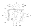
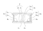
- FIG. 1 is a cross-sectional view showing an etalon device in a variable spectral element according to Example 1.
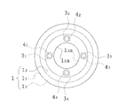
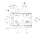
- FIG. 3 is a plan view of the etalon device of FIG. 2.
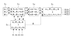
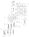
- FIG. 3 is a block diagram illustrating a calculation performed by a control unit in the variable spectral element according to the first embodiment.
- FIG. 3 is a block diagram schematically illustrating an overall control configuration of the variable spectral element according to the first embodiment.
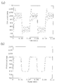
- 3 is a graph showing response characteristics of the etalon device of FIG. 2, (a) is a graph when the surface separation is controlled by a conventional variable spectroscopic element, and (b) is a surface control by the variable spectroscopic device of the present embodiment. It is a graph when it is done.
- FIG. 10 is a block diagram illustrating a calculation performed by a control unit in a variable spectral element according to a second embodiment.
- FIG. 10 is a block diagram schematically illustrating an overall control configuration of a variable spectral element according to a second embodiment.
- FIG. 10 is a block diagram schematically illustrating an overall control configuration of a variable spectral element according to a third embodiment.
- FIG. 10 is a block diagram schematically illustrating an overall control configuration of a variable spectral element according to a fourth embodiment.
- FIG. 10 is a block diagram illustrating a calculation performed by a control unit in a variable spectral element according to a second embodiment.
- FIG. 10 is a block diagram schematically illustrating an overall control configuration of a variable spectral element according to a second embodiment.
- FIG. 10 is a block diagram schematically illustrating an overall control configuration of a variable spectral element according to a third embodiment.
- FIG. 10 is a block diagram schematically illustrating an overall control configuration of
- FIG. 6 is a plan view showing a first modification of the etalon device of FIG. 2. It is a top view which shows the 2nd modification of the etalon apparatus of FIG. It is a top view which shows the 3rd modification of the etalon apparatus of FIG. It is a top view which shows the 4th modification of the etalon apparatus of FIG.
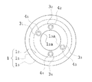
- FIG. 10 is a cross-sectional view illustrating an etalon device in a variable spectral element according to a fifth embodiment.
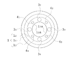
- FIG. 18 is a plan view of the etalon device of FIG. 17.
- FIG. 2 is a cross-sectional view showing the etalon device in the variable spectral element according to the present embodiment.
- FIG. 3 is a plan view of the etalon device of FIG.
- FIG. 4 is a schematic diagram showing the operation of a pair of optical substrates and four piezoelectric elements of the etalon device of FIG.
- FIG. 5 is a block diagram illustrating calculation performed by the control unit in the variable spectral element according to the first embodiment.
- FIG. 6 is a block diagram schematically illustrating the overall control configuration of the variable spectral element according to the first embodiment.
- FIG. 7 is a graph showing the response characteristics of the etalon device of FIG. 2, (a) is a graph when the surface spacing is controlled by a conventional variable spectroscopic element, and (b) is a surface by the variable spectroscopic element of this embodiment. It is a graph when an interval is controlled.
- variable spectroscopic element is configured by the etalon device shown in FIGS. 2 and 3 and a control unit (not shown).
- this etalon device includes a pair of optical substrates 2 in the outer frame 1 and a capacitance that is a means for measuring a surface interval between the opposing surfaces of the pair of optical substrates 2.
- An actuator for moving the sensor and one of the pair of optical substrates 2 includes a piezo element whose drive is controlled by a control unit (not shown).
- the outer frame 1, the annular member 1 2 in one end surface of the tubular member 1 1 is constituted by attaching the annular member 1 3 on the other.
- circular openings 1 2 a and 1 3 a are formed in the annular members 1 2 and 1 3 at substantially the center thereof. In this etalon device, the openings 1 2 a and 1 3 are formed. Light passes through a.
- the pair of optical substrates 2 includes a fixed substrate 2 1 and a movable substrate 2 2 which are arranged so that opposing surfaces are parallel to each other with a space therebetween.
- the fixed substrate 2 1 the opening 1 2 a in the interior of the outer frame 1, 1 3 disc which is fixed to the annular member 1 2 of the outer frame 1 so as to cross the axis of the light passing through the a Shaped optical member.
- the movable substrate 2 2 is a disc-shaped optical member held by the piezo element so as to cross the light passing through the openings 1 2 a and 1 3 a.
- the movable substrate 2 2 has a direction along the axis of light passing through the openings 1 2 a and 1 3 a, that is, the center of gravity of each of the opposing surfaces of the pair of optical substrates.
- the first capacitance sensor 3 1 , the second capacitance sensor 3 2 , the third capacitance sensor 3 3 , and the fourth capacitance sensor 3 4 have a pair of electrodes 3 11 , 3 12 , 3 21 , respectively. And 3 22 , 3 31 and 3 32 , 3 41 and 3 42 .
- the pair of electrodes are opposed to each other at positions where the light passing through the openings 1 2 a and 1 3 a of the outer frame 1 is not blocked on the opposing surfaces of the pair of optical substrates 2. are arranged.
- these capacitance sensors have a characteristic that the capacitance between the electrodes changes in inverse proportion to the surface spacing.
- the value acquired by these capacitance sensors is converted into the surface interval value of the optical substrate 2 and output to a control unit (not shown).
- the first piezo element 4 1 , the second piezo element 4 2 , the third piezo element 4 3 , and the fourth piezo element 4 4 respectively transmit the light passing through the openings 1 2 a and 1 3 a inside the outer frame 1. It is fixed to the annular member 1 3 of the outer frame 1 so as not to block.
- the first piezo element 4 1 is the first capacitance sensor 3 1
- the second piezo element 4 2 is the second capacitance sensor 3 2
- the third piezo element 4 3 is the third capacitance sensor 3.
- the fourth piezo element 4 4 are arranged at an overlapping position when viewed from the direction along the line connecting the centroids of the surfaces of the fourth electrostatic capacitance sensor 3 4 and the pair of optical substrates 2 facing each other. .
- the first capacitance sensor 3 1 and the first piezo element 4 1 , and the third capacitance sensor 3 3 and the third piezo element 4 3 are respectively centroids of the opposing surfaces of the pair of optical substrates 2. As viewed from the direction along the line connecting the centroids, they are arranged at positions symmetrical with respect to the line connecting the centers of gravity.
- the second capacitance sensor 3 2 and the second piezo element 4 2 , and the fourth capacitance sensor 3 4 and the fourth piezo element 4 4 are respectively centroids of the opposing surfaces of the pair of optical substrates 2. As viewed from the direction along the line connecting the centroids, they are arranged at positions symmetrical with respect to the line connecting the centers of gravity.
- the first capacitance sensor 3 1 and the first piezo element 4 1 , the second capacitance sensor 3 2 and the second piezo element 4 2 , the third capacitance sensor 3 3 and the third piezo element 4. 3 and the fourth capacitance sensor 3 4 and the fourth piezo element 4 4 are arranged at equal intervals as viewed from the direction along the line connecting the centers of gravity of the opposing surfaces of the pair of optical substrates 2. Yes.
- the first piezo element 4 1 is accurately driven to set the surface distance between the pair of optical substrates 2 at the position where the first capacitance sensor 3 1 is set to the target value x 0. also, then, the interference caused when the first piezoelectric element 4 1 second piezoelectric element 4 2 and 4 piezoelectric element 4 4 which is arranged adjacent to the drive surface distance from the target value x 0 Sometimes changed.
- examples of the resolution method there is a method employing a feedback control such as PID control (Proportional Integral Derivative Control), in which case the need a long time to surface distance of the optical substrate is a target value x 0 It is.
- PID control Proportional Integral Derivative Control
- variable spectroscopic element the four output values from the first to fourth capacitance sensors 3 1 , 3 2 , 3 3 , and 3 4 are converted into three parameters for calculation,
- the first to fourth piezo elements 4 1 , 4 2 , 4 3 and 4 4 are controlled.
- variable spectroscopic element of this embodiment as shown in FIG. 4, when the movable substrate 2 2 is moved with respect to the fixed substrate 2 1 and the surface interval between the pair of optical substrates 2 is set to x 0 , as shown in FIG. 5 and FIG. 5, via the target input unit 5 1 to the control unit, the interval between the center of gravity G 2 opposing faces of the center of gravity G 1 and the movable substrate 2 2 opposing surfaces of the fixed substrate 2 1 target value x 0, the target value phi 0 of the target value theta 0 and the second angle of the first angle and those of the opposite sides of the center of gravity plane perpendicular the movable substrate in a line connecting between 2 2 forms input.
- the sensor output conversion unit 5 2 includes a pair of optical substrates 2 at the arrangement positions of the capacitance sensors measured by the first to fourth capacitance sensors 3 1 , 3 2 , 3 3 , 3 4 .
- the first to fourth piezoelectric elements 4 1 to 4 4 are respectively opposed to the first to fourth capacitance sensors 3 1 to 3 4 and the pair of optical substrates 2 facing each other. As seen from the direction along the line connecting the centroids of the two, they are arranged at overlapping positions. For this reason, the inter-surface distances x 41 , x 42 , x 43 , x 44 between the opposing surfaces of the pair of optical substrates 2 at the arrangement positions of the first to fourth piezo elements 4 1 to 4 4 are the first to fourth. The distances between the opposing surfaces of the pair of optical substrates 2 at the positions where the capacitive sensors 3 1 to 3 4 are disposed coincide with the distances x 1 , x 2 , x 3 , x 4 .
- the first angle ⁇ and the second angle ⁇ formed by the surface perpendicular to the line connecting the centers of gravity of the opposed surfaces of the pair of optical substrates 2 and the surface of the movable substrate 2 2 facing the fixed substrate 2 1.
- the first to fourth capacitive sensor from the center of gravity G 2 of opposing surfaces of the movable substrate 2 2 is a known value 3 1, 3 2, 3 3, 3 4 electrodes 3 12, 3 22, 3 32 , by using the distance r 31, r 32, r 33 , r 34 of 3 to 42 the center of the fixed substrate 2 2 opposite the surface, the following equation holds.
- sin ⁇ (x 3 ⁇ x 1 ) / (r 31 + r 33 )
- sin ⁇ (x 4 ⁇ x 2 ) / (r 32 + r 34 )
- the difference value calculating unit 3 a target value input via the target value input section 5 1 x 0, ⁇ 0, and phi 0, converted by the sensor output converting unit 5 2 x, theta, phi
- the difference values ex, e ⁇ , e ⁇ are calculated.
- the command value calculating unit 4 performs PID control based differential value ex is calculated by the difference value calculator 5 3, E.theta, the E?, Obtains the command value xc, .theta.c, the .phi.c.
- the command value converter 5 5 the command values xc, ⁇ c, and ⁇ c obtained by the command value calculator 5 4 are used as commands for the first to fourth piezo elements 4 1 , 4 2 , 4 3 , 4 4. Convert to values x c1 , x c2 , x c3 , x c4 .
- the command value conversion unit 5 5 is configured such that the optical substrate surface interval x 1 and the second capacitance sensor 3 2 are arranged at the arrangement position of the first capacitance sensor 3 1 calculated by the sensor output conversion unit 5 2.
- the corrected command values x c1 ′, x c2 ′, x c3 ′, and x c4 ′ are supplied to piezo element drivers (not shown) that drive the corresponding first to fourth piezo elements 4 1 , 4 2 , 4 3 , and 4 4 , respectively.
- the drive voltage is applied to each of the first to fourth piezo elements 4 1 , 4 2 , 4 3 , 4 4 by the piezo element input driver.
- the command values x c1 , x c2 , x c3 , and x c4 for the first to fourth piezo elements 4 1 , 4 2 , 4 3 , and 4 4 are known values that are the first to fourth piezo elements. Using the distances r 41 , r 42 , r 43 , r 44 on the opposing surface of the fixed substrate 2 2 to the center of the elements 4 1 , 4 2 , 4 3 , 4 4 , the following equation is established.
- each of the first to fourth piezo elements 4 1 , 4 2 , 4 3 , 4 4 The command values x c1 , x c2 , x c3 , and x c4 for are obtained by the following equations.
- x c1 , x c2 , x c3 , x c4 are corrected as in the following expressions x c1 ′, x c2 ′, x c3 ′, x c4 ′.
- x c1 ′ x ⁇ r ⁇ c ⁇ ( ⁇ / 2)
- x c2 ′ x ⁇ r ⁇ c + ( ⁇ / 2)
- x c3 ′ x + r ⁇ c ⁇ ( ⁇ / 2)
- x c4 ′ x + r ⁇ c + ( ⁇ / 2)
- the first to fourth piezo elements 4 1 , 4 2 , 4 3 , and 4 4 are changed to the command values x c1 ′, x c2 ′, x c3 ′, and x c4 ′ corrected as shown in the above formulas. based driven by a voltage applied by the piezoelectric element driver, by moving the movable substrate 2 2, changing the surface interval x of the pair of optical substrates 2.
- variable spectroscopic element is based on these control processes in the sensor output conversion unit 5 2 , the difference value calculation unit 5 3 , the command value calculation unit 5 4 , and the command value conversion unit 5 5, and the control processes thereof.
- FIG. 7 is a graph showing experimental results regarding response characteristics of the etalon device when feedback control is performed in the variable spectroscopic element.
- the vertical axis represents the surface spacing (nm) between the pair of optical substrates
- the horizontal axis represents time (sec)
- (a) is the experimental result of a conventional variable spectral element
- (b) is the variable spectral element of this example. It is an experimental result by.
- a signal is input by switching the target value every 0.02 seconds.
- the diameter of the used etalon optical substrate is about 10 mm, and a command is issued to control the surface interval to move between 800 nm and 1000 nm every 0.02 seconds.
- variable spectroscopic element of this example has a very short time until the distance between the surfaces of the pair of optical substrates converges as compared with the conventional variable spectroscopic element. Therefore, the variable spectroscopic element of the present invention can accurately change the optical characteristics even when the optical characteristics are continuously and rapidly changed.
- the command value converting portion 5 5, the sensor output conversion unit 5 2 surface spacing x 1 optical substrates in a first capacitive sensor 3 1 of the arrangement position calculated in the second capacitance Since the control for correcting the deflection of the optical substrate is performed by using the difference value ⁇ with respect to the surface interval x 2 of the optical substrate at the position where the sensor 3 2 is arranged, even if the piezo characteristics of each axis vary, The center of gravity position and rotation angle of the optical substrate can be adjusted in consideration of variations.
- FIG. 8 is a graph showing the spectral sensitivity of a variable optical element having a deflection on the optical substrate and the spectral sensitivity of a variable optical element having no deflection on the optical substrate.
- an optical substrate having a deflection of about 50 nm was used as the variable optical element having deflection used in the data of FIG. 8.
- variable optical element having a deflection on the optical substrate and the variable optical element having no deflection on the optical substrate are set so that the sensitivity is maximized at a wavelength of 600 nm.
- a deflection amount of about 5 nm is generated, and when the optical substrate is bent, a deflection amount of 50 nm is generated, and the distance between the optical substrates is controlled to be 600 nm.
- the spectral sensitivity characteristics in this state were measured using an optical spectrum analyzer.
- the variable optical element having no deflection on the optical substrate has a sharp peak wavelength.
- the variable optical element having the deflection on the optical substrate has poor spectral sensitivity, and the peak wavelength spreads horizontally.
- variable spectroscopic element that does not include the deflection control means described in Japanese Patent Application No. 2011-209574 can eliminate the deflection of the optical substrate when there is a variation in the actuator characteristics of the optical substrate. Therefore, the optical characteristics cannot be changed accurately.
- the variable spectroscopic element according to the present embodiment includes the deflection control means, it is possible to prevent the optical substrate from being bent even if there is a variation in the actuator characteristics in two directions provided in the optical substrate. . For this reason, according to the variable optical element of the present embodiment, the optical characteristics can be accurately changed at high speed regardless of variations in the characteristics of the two-direction actuator provided in the etalon.
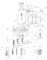
- FIG. 9 is a block diagram illustrating an operation performed by the control unit in the variable spectral element according to the second embodiment
- FIG. 10 is a block diagram schematically illustrating an overall control configuration of the variable spectral element according to the second embodiment.
- the second embodiment is an example applicable to a case where the difference in the position of the optical substrate between the positions of the opposing actuators is large and it is difficult to control the rotation angle of the optical substrate with high accuracy. When the difference in characteristics between the opposing actuators is large, the accuracy of controlling the rotation angle of the optical substrate is deteriorated.
- variable optical element the average distance between the optical substrates at the position of the opposing actuator in the first direction and the surface distance of the optical substrate at the position of the opposing actuator in the second direction. It is comprised so that bending control may be performed using the difference with the average of.
- the configuration of the etalon device is the same as that of the first embodiment shown in FIGS.
- the corrected command values x c1 ", x c2 ", x c3 “, x c4 " are supplied to piezoelectric element drivers (not shown) that drive the corresponding first to fourth piezoelectric elements 4 1 , 4 2 , 4 3 , 4 4 , respectively.
- the drive voltage is applied to each of the first to fourth piezo elements 4 1 , 4 2 , 4 3 , 4 4 by the piezo element input driver.
- the command values x c1 , x c2 , x c3 , and x c4 for the first to fourth piezo elements 4 1 , 4 2 , 4 3 , and 4 4 are known values that are the first to fourth piezo elements. Using the distances r 41 , r 42 , r 43 , r 44 on the opposing surface of the fixed substrate 2 2 to the center of the elements 4 1 , 4 2 , 4 3 , 4 4 , the following equation is established.
- each of the first to fourth piezo elements 4 1 , 4 2 , 4 3 , 4 4 The command values x c1 , x c2 , x c3 , and x c4 for are obtained by the following equations.
- x c1 x ⁇ r ⁇ c ⁇ ( ⁇ ′ / 2)
- x c2 x ⁇ r ⁇ c + ( ⁇ ′ / 2)
- x c3 x + r ⁇ c- ( ⁇ '/ 2)
- x c4 x + r ⁇ c + ( ⁇ '/ 2)
- the first to fourth piezo elements 4 1 , 4 2 , 4 3 , and 4 4 are changed to the command values x c1 ", x c2 ", x c3 ", and x c4 " corrected as shown in the above equations. based driven by a voltage applied by the piezoelectric element driver, by moving the movable substrate 2 2, changing the surface interval x of the pair of optical substrates 2.
- variable spectroscopic element is based on these control processes in the sensor output conversion unit 5 2 , the difference value calculation unit 5 3 , the command value calculation unit 5 4 , and the command value conversion unit 5 5, and the control processes thereof.
- the rotation angle of the optical substrate can be controlled with high accuracy even when the difference in characteristics between the actuators facing each other is large.
- the optical characteristics can be changed more accurately.
- FIG. 11 is a block diagram schematically illustrating an overall control configuration of the variable spectral element according to the third embodiment.
- the variable spectroscopic element of the third embodiment cancels the characteristic difference between the actuators with respect to each of the first to fourth actuators when the variable control unit 5 is operated.
- a characteristic difference correction voltage application unit 6 for applying an offset voltage for the purpose is provided.
- the characteristic difference correction voltage application unit 6 stores, for example, a fixed offset voltage value set in advance for canceling the characteristic difference between the piezoelectric elements for each of the first to fourth piezoelectric elements 4 1 to 4 4.
- a ROM (not shown) is configured, and when the control unit 5 operates, a predetermined offset voltage is applied to each of the channels of the first to fourth piezo elements 4 1 to 4 4 .
- the characteristic difference correction voltage applying unit 6 includes a temperature / humidity sensor (not shown) and driving characteristics (inputs) of the first to fourth piezo elements 4 1 to 4 4 using temperature / humidity information as a key in addition to the ROM.
- the temperature / humidity information detected in real time by the temperature / humidity sensor when the control unit 5 is operated, it is configured with a so-called look-up table (not shown) that stores offset voltage data according to the voltage expansion / contraction amount).
- the offset voltage applied to each channel of the first to fourth piezo elements 4 1 to 4 4 may be switched.
- the characteristic difference correction voltage applying unit 6 is the first to fourth actuators. Since the characteristic difference between the fourth piezo elements 4 1 to 4 4 is reduced as much as possible, the calculation load of the control unit 5 can be reduced, and the optical characteristics can be changed with high speed and high accuracy accordingly.
- the characteristic difference correction voltage application unit 6 is composed of a ROM (not shown) that stores a fixed offset voltage value, the configuration can be simplified.
- the characteristic difference correction voltage application unit 6 is configured to switch the offset voltage in real time, it can cope with fluctuations in the characteristics of the piezo element due to environmental fluctuations and changes with time, and can change the optical characteristics with high accuracy. Can do.
- Other functions and effects are substantially the same as those of the variable optical element of the first embodiment.
- FIG. 12 is a block diagram schematically illustrating an overall control configuration of the variable spectral element according to the fourth embodiment.
- the variable spectroscopic element according to the fourth embodiment cancels the characteristic difference between the actuators with respect to each of the first to fourth actuators when the variable control unit 5 is operated.
- a characteristic difference correction voltage application unit 6 for applying an offset voltage for the purpose is provided.
- the configuration of the characteristic difference correction voltage application unit 6 is substantially the same as the characteristic difference correction voltage application unit in the variable optical element of Example 3.
- the characteristic difference correction voltage applying unit 6 is the first to fourth actuators. Since the characteristic difference between the fourth piezo elements 4 1 to 4 4 is reduced as much as possible, the calculation load of the control unit 5 can be reduced, and the optical characteristics can be changed with high speed and high accuracy accordingly. This is particularly effective when the characteristic difference between the first to fourth piezo elements 4 1 to 4 4 is large and it is difficult to control the rotation angle of the optical substrate.
- the characteristic difference correction voltage application unit 6 is composed of a ROM (not shown) that stores a fixed offset voltage value, the configuration can be simplified.
- the characteristic difference correction voltage application unit 6 when configured to switch the offset voltage in real time, it can cope with fluctuations in the characteristics of the piezo element due to environmental fluctuations and changes with time, and can change the optical characteristics with high accuracy. Can do. Other functions and effects are substantially the same as those of the variable optical element of the second embodiment.
- FIG. 13 is a plan view showing a first modification of the etalon device of FIG.
- FIG. 14 is a plan view showing a second modification of the etalon device of FIG.
- FIG. 15 is a plan view showing a third modification of the etalon device of FIG.
- FIG. 16 is a cross-sectional view showing a fourth modification of the etalon device of FIG.
- first and first capacitive sensor 3 1 and the first piezoelectric element 4 are opposed surfaces of the pair of optical substrates 2. They are not arranged at regular intervals as viewed from the direction along the line connecting the centers of gravity.
- the first capacitance sensor 3 1, the first piezo element 4 1 , the third capacitance sensor 3 3, the third piezo element 4 3 , and the second capacitance sensor 3. 2 and the second piezo element 4 2 , the fourth capacitance sensor 3 4 and the fourth piezo element 4 4 as viewed from the direction along the line connecting the centers of gravity of the opposing surfaces of the pair of optical substrates 2.
- the control unit can perform control by performing the same calculation as the etalon device of the variable spectroscopic element of each of the above embodiments.
- the etalon device shown in FIGS. 14 and 15 is different from the etalon device of the variable spectroscopic element of each of the embodiments described above, and the first capacitance sensor 3 1 , the first piezo element 4 1 , the second capacitance sensor 3 2, and The second piezo element 4 2 , the third capacitance sensor 3 3, the third piezo element 4 3 , the fourth capacitance sensor 3 4, and the fourth piezo element 4 4 are disposed on the opposing surfaces of the pair of optical substrates 2. They are arranged at positions that do not overlap as seen from the direction along the line connecting the centers of gravity.
- the first to fourth piezo elements 4 1 , 4 2 , 4 3 can be performed by performing the same calculation as the etalon device of the variable spectroscopic element.
- the etalon device shown in FIG. 16 is different from the etalon device in the variable spectroscopic element of each of the above embodiments, and does not include the outer frame 1, and the first piezo element 4 1 , the second piezo element 4 2 , and the third piezo element 4. 3, the fourth piezoelectric element 4 4 are each, so as not to block the light passing through the etalon device, it is fixed to the fixed substrate 2 1 opposite the surface.
- control can be performed by performing the same calculation as the etalon device in the variable spectroscopic element of the above embodiment in the control unit.
- a fifth embodiment of a variable spectral element having an etalon device which is a variable spectral element according to the present invention, will be described with reference to FIGS.
- the member which comprises the etalon apparatus in the variable spectroscopy element of Example 5 is the same as the member which comprises the etalon apparatus of Example 1, while attaching the same code
- the configuration of the control unit in the variable spectroscopic element of Example 5 and the calculations performed therein are substantially the same as the calculations performed in the control unit of the variable spectroscopic element of Example 1, so a detailed description thereof will be given. Omitted.
- FIG. 17 is a cross-sectional view showing the etalon device in the variable spectral element according to the present embodiment.
- 18 is a plan view of the etalon device of FIG.
- the first to fourth piezo elements 4 1 , 4 2 , 4 3 , 4 4 and the first to fourth piezo elements are annularly formed so as to be alternately spaced at an equal interval when viewed from the direction along the line connecting the centers of gravity of the opposing surfaces of the pair of optical substrates 2. Has been placed.
- the distance x between the centers of gravity of the opposing surfaces of the pair of optical substrates 2 is determined from the output values of the first to fourth capacitance sensors 3 1 , 3 2 , 3 3 , 3 4.
- the first angle ⁇ is calculated from the output values of the first and third capacitance sensors 3 1 and 3 3
- the second angle is calculated from the output values of the second and fourth capacitance sensors 3 2 and 3 4 .
- the angle ⁇ is calculated.
- the driving of the first and third piezo elements 4 1 and 4 3 is controlled based on the distance x between the centroids and the first angle ⁇ , and the driving of the second and fourth piezo elements 4 2 and 4 4 is controlled.
- variable spectroscopic element of the fifth embodiment using all output values of the first to fourth capacitance sensors 3 1 , 3 2 , 3 3 , 3 4 , the distance x between the centroids and a pair of The inter-surface spacings x 41 , x 42 , x 43 , x of the pair of optical substrates 2 at the arrangement positions of the first to fourth piezo elements 4 1 , 4 2 , 4 3 , 4 4 on the optical substrate 2. 44 is calculated, and the first angle ⁇ and the second angle ⁇ are calculated using the calculated surface intervals x 41 , x 42 , x 43 , x 44 .
- the first to fourth piezo elements 4 1 , 4 2 , 4 3 , 4 4 are driven by the distance x between the centers of gravity, the first angle ⁇ , and the second angle.
- the mean and the second position of the piezoelectric element 4 2 of the first piezoelectric element 4 1 surface distance x 41 optical substrates at the arrangement position of the third spacing of the optical substrate at the arrangement position of the piezoelectric element 4 3 x 43 difference value between the average surface distance x 44 optical substrate surface spacing x 42 optical substrate and in the fourth position of the piezoelectric element 4 4 ⁇ '(
- the capacitance sensor 3 and the corresponding piezo element 4 are viewed from the direction along the line connecting the centers of gravity of the opposing surfaces of the pair of optical substrates 2.
- the distances x 1 , x 2 , x 3 , x 4 between the opposing surfaces of the pair of optical substrates 2 detected by the capacitance sensor 3 are set as the first to fourth piezoelectric elements. Since the optical substrate plane distances x 41 , x 42 , x 43 , and x 44 at the positions 4 1 , 4 2 , 4 3 , and 4 4 are converted, the same control as in the first embodiment can be performed. .
- variable spectroscopic element of Example 5 can accurately change the optical characteristics even when the optical characteristics are continuously and rapidly changed.
- ), or the surface spacing x 41 optical substrates in the first piezoelectric element 4 1 position the 3 of the optical substrate at the arrangement position of the piezoelectric element 4 3 surface spacing x 43 average and a surface spacing x 42 optical substrates of the second piezoelectric element 4 2 of the arrangement position of the optical substrate in a fourth position of the piezoelectric element 4 4 Since the difference value ⁇ ′ (
Landscapes
- Physics & Mathematics (AREA)
- Spectroscopy & Molecular Physics (AREA)
- General Physics & Mathematics (AREA)
- Optics & Photonics (AREA)
- Nonlinear Science (AREA)
- Mechanical Light Control Or Optical Switches (AREA)
- Spectrometry And Color Measurement (AREA)
Priority Applications (1)
| Application Number | Priority Date | Filing Date | Title |
|---|---|---|---|
| US13/955,658 US9383596B2 (en) | 2011-02-01 | 2013-07-31 | Variable spectrum element |
Applications Claiming Priority (2)
| Application Number | Priority Date | Filing Date | Title |
|---|---|---|---|
| JP2011-019706 | 2011-02-01 | ||
| JP2011019706A JP5530375B2 (ja) | 2011-02-01 | 2011-02-01 | 可変分光素子 |
Related Child Applications (1)
| Application Number | Title | Priority Date | Filing Date |
|---|---|---|---|
| US13/955,658 Continuation US9383596B2 (en) | 2011-02-01 | 2013-07-31 | Variable spectrum element |
Publications (1)
| Publication Number | Publication Date |
|---|---|
| WO2012105455A1 true WO2012105455A1 (ja) | 2012-08-09 |
Family
ID=46602671
Family Applications (1)
| Application Number | Title | Priority Date | Filing Date |
|---|---|---|---|
| PCT/JP2012/051858 Ceased WO2012105455A1 (ja) | 2011-02-01 | 2012-01-27 | 可変分光素子 |
Country Status (3)
| Country | Link |
|---|---|
| US (1) | US9383596B2 (enExample) |
| JP (1) | JP5530375B2 (enExample) |
| WO (1) | WO2012105455A1 (enExample) |
Families Citing this family (1)
| Publication number | Priority date | Publication date | Assignee | Title |
|---|---|---|---|---|
| US10088670B1 (en) * | 2015-03-20 | 2018-10-02 | C. Anthony Hester | Interference based spatial light modulator systems and methods |
Citations (3)
| Publication number | Priority date | Publication date | Assignee | Title |
|---|---|---|---|---|
| JP2008151544A (ja) * | 2006-12-14 | 2008-07-03 | Olympus Corp | 可変分光素子、分光装置および内視鏡システム |
| JP2010224011A (ja) * | 2009-03-19 | 2010-10-07 | Olympus Corp | エタロン装置及びそれを備えた光学ユニット |
| JP2011209574A (ja) * | 2010-03-30 | 2011-10-20 | Olympus Corp | 可変分光素子 |
Family Cites Families (7)
| Publication number | Priority date | Publication date | Assignee | Title |
|---|---|---|---|---|
| JPH06241899A (ja) | 1993-01-29 | 1994-09-02 | Shimadzu Corp | エタロン駆動機構 |
| JP3812550B2 (ja) * | 2003-07-07 | 2006-08-23 | セイコーエプソン株式会社 | 波長可変光フィルタ |
| JP5085101B2 (ja) * | 2006-11-17 | 2012-11-28 | オリンパス株式会社 | 可変分光素子 |
| JP2008183350A (ja) * | 2007-01-31 | 2008-08-14 | Olympus Corp | 可変分光素子、分光装置および内視鏡システム |
| JP2008197362A (ja) * | 2007-02-13 | 2008-08-28 | Olympus Corp | 可変分光素子 |
| JP5798709B2 (ja) * | 2009-03-04 | 2015-10-21 | セイコーエプソン株式会社 | 光フィルター及びそれを備えた光モジュール |
| JP5363394B2 (ja) * | 2010-03-30 | 2013-12-11 | オリンパス株式会社 | 可変分光素子 |
-
2011
- 2011-02-01 JP JP2011019706A patent/JP5530375B2/ja not_active Expired - Fee Related
-
2012
- 2012-01-27 WO PCT/JP2012/051858 patent/WO2012105455A1/ja not_active Ceased
-
2013
- 2013-07-31 US US13/955,658 patent/US9383596B2/en not_active Expired - Fee Related
Patent Citations (3)
| Publication number | Priority date | Publication date | Assignee | Title |
|---|---|---|---|---|
| JP2008151544A (ja) * | 2006-12-14 | 2008-07-03 | Olympus Corp | 可変分光素子、分光装置および内視鏡システム |
| JP2010224011A (ja) * | 2009-03-19 | 2010-10-07 | Olympus Corp | エタロン装置及びそれを備えた光学ユニット |
| JP2011209574A (ja) * | 2010-03-30 | 2011-10-20 | Olympus Corp | 可変分光素子 |
Also Published As
| Publication number | Publication date |
|---|---|
| US20140036344A1 (en) | 2014-02-06 |
| JP2012159719A (ja) | 2012-08-23 |
| JP5530375B2 (ja) | 2014-06-25 |
| US9383596B2 (en) | 2016-07-05 |
Similar Documents
| Publication | Publication Date | Title |
|---|---|---|
| JP5519067B1 (ja) | 光学干渉計、及びこれを用いたフーリエ変換型分光器 | |
| US8259300B2 (en) | Interferometer actuator | |
| JP2014153389A5 (enExample) | ||
| US20150270477A1 (en) | Actuator | |
| JP5363393B2 (ja) | 可変分光素子 | |
| CN110799883B (zh) | 光学装置 | |
| WO2016097127A1 (en) | A quadrature compensation method for mems gyroscopes and a gyroscope sensor | |
| CN102822720B (zh) | 可变分光元件 | |
| JP5530375B2 (ja) | 可変分光素子 | |
| US11060909B2 (en) | Spectrometer, analysis equipment, and wavelength-variable light source | |
| CN104541130B (zh) | 回转角加速度测定装置 | |
| JP2010224011A (ja) | エタロン装置及びそれを備えた光学ユニット | |
| JP2011209574A5 (enExample) | ||
| JP4135054B2 (ja) | 光干渉計用移動ミラー支持装置 | |
| US9086302B2 (en) | Measuring element | |
| JP2011033368A (ja) | 光学式エンコーダ | |
| JP2015231643A (ja) | 回転型アクチュエータ及び回転型アクチュエータの制御方法 | |
| TW202000576A (zh) | 微機電感測器 | |
| KR20160008445A (ko) | 액추에이터 유닛 및 렌즈 모듈 | |
| JP2020115098A5 (ja) | 角速度センサー、慣性計測装置、電子機器および移動体 | |
| JP2013164397A (ja) | エンコーダ用スケールユニットおよびエンコーダ | |
| JP2015060108A (ja) | 波長選択スイッチの製造方法 | |
| WO2019009393A1 (ja) | 光学デバイス及びその製造方法 | |
| JP2012143294A (ja) | 可変分光素子、分光装置および内視鏡装置 | |
| WO2010023767A1 (ja) | 変位センサ |
Legal Events
| Date | Code | Title | Description |
|---|---|---|---|
| 121 | Ep: the epo has been informed by wipo that ep was designated in this application |
Ref document number: 12741819 Country of ref document: EP Kind code of ref document: A1 |
|
| NENP | Non-entry into the national phase |
Ref country code: DE |
|
| 122 | Ep: pct application non-entry in european phase |
Ref document number: 12741819 Country of ref document: EP Kind code of ref document: A1 |