WO2012102113A1 - モータ制御装置 - Google Patents
モータ制御装置 Download PDFInfo
- Publication number
- WO2012102113A1 WO2012102113A1 PCT/JP2012/050731 JP2012050731W WO2012102113A1 WO 2012102113 A1 WO2012102113 A1 WO 2012102113A1 JP 2012050731 W JP2012050731 W JP 2012050731W WO 2012102113 A1 WO2012102113 A1 WO 2012102113A1
- Authority
- WO
- WIPO (PCT)
- Prior art keywords
- circuit
- current
- phase
- motor control
- control device
- Prior art date
- Legal status (The legal status is an assumption and is not a legal conclusion. Google has not performed a legal analysis and makes no representation as to the accuracy of the status listed.)
- Ceased
Links
Images



Classifications
-
- H—ELECTRICITY
- H02—GENERATION; CONVERSION OR DISTRIBUTION OF ELECTRIC POWER
- H02P—CONTROL OR REGULATION OF ELECTRIC MOTORS, ELECTRIC GENERATORS OR DYNAMO-ELECTRIC CONVERTERS; CONTROLLING TRANSFORMERS, REACTORS OR CHOKE COILS
- H02P6/00—Arrangements for controlling synchronous motors or other dynamo-electric motors using electronic commutation dependent on the rotor position; Electronic commutators therefor
- H02P6/12—Monitoring commutation; Providing indication of commutation failure
Definitions
- the present invention mainly relates to a motor control device for controlling a three-phase motor used in an in-vehicle electric power steering device, an electric water pump device, an electric oil pump device, an inverter device and the like.
- the present invention relates to a motor control device capable of continuing stable motor driving even when an abnormality occurs.
- an electric motor that performs torque assist using a motor instead of a conventional hydraulic power assist device for the purpose of improving fuel efficiency by reducing vehicle weight.
- a power steering device (EPS) has been introduced.
- the electric power steering apparatus does not always need to rotate the hydraulic pump, and assists the driving force by rotating the motor only when necessary. Therefore, it is effective in improving fuel consumption.
- a three-phase brushless DC motor that is relatively agile and can generate high torque and is easy to control is used as an assist motor for an electric power steering apparatus.
- a semiconductor switch element is generally used to generate the driving power of the motor from the DC power.
- disturbances such as inductive noise and transient surges caused by external factors may cause a failure of the semiconductor switch element. Therefore, various techniques for detecting a failure of the semiconductor switch element are known.
- Patent Document 1 discloses the following technique in a drive circuit of a three-phase brushless DC motor. That is, the output voltage of each phase of the motor is detected, and if any one phase voltage does not satisfy the desired voltage, it is determined that the semiconductor switch element is abnormal. And the power supply of a three-phase drive circuit is interrupted
- Patent Document 2 discloses the following technique in an inverter circuit for driving a three-phase AC motor. That is, for each phase of the motor to be driven, a semiconductor switch element and a fuse are respectively provided on the power supply side (high side) and the ground side (low side) in the inverter circuit. By detecting that the fuse is blown by the failure diagnosis device, the failure of the semiconductor switch element of each phase is detected. Then, the motor is urgently operated by two-phase driving.
- the motor control device is for controlling a three-phase motor, and is provided with a semiconductor switch element provided for each phase of the three-phase motor to drive the three-phase motor; A pre-driver circuit provided for each phase of the three-phase motor to control the operation of the semiconductor switch element, a power supply circuit that supplies current to the pre-driver circuit, and an arithmetic processing device that calculates and outputs a motor control signal And a logic circuit that outputs a drive signal for each phase of the three-phase motor based on the motor control signal output from the arithmetic processing unit, and an operation of the pre-driver circuit based on the drive signal output from the logic circuit.
- the semiconductor switch element is provided on the high voltage side of each phase, and on the low voltage side of each phase.
- the low-side semiconductor switch element is preferably included.
- the pre-driver circuit includes a high-side push-pull circuit provided corresponding to the high-side semiconductor switch element of each phase and a low-side push-pull circuit provided corresponding to the low-side semiconductor switch element of each phase. It is preferable to include. Furthermore, it is preferable that the current interrupting circuit interrupts the supply of current to at least one of the high-side push-pull circuit and the low-side push-pull circuit.
- the current cutoff circuit includes a voltage follower circuit provided between the power supply circuit and the pre-driver circuit, and a current magnitude. And a current detection circuit for detecting. When the magnitude of the current detected by the current detection circuit is greater than or equal to a predetermined value, it is preferable to cut off the supply of current from the power supply circuit to the pre-driver circuit by changing the output voltage of the voltage follower circuit.
- the current interrupt circuit may include an overcurrent interrupt fuse provided between the power supply circuit and the pre-driver circuit.
- the magnitude of the current is greater than or equal to a predetermined value, it is preferable to cut off the supply of current from the power supply circuit to the pre-driver circuit by melting the overcurrent cutoff fuse.
- the pre-driver circuit includes a plurality of push-pulls connected in parallel to the power supply circuit for each phase of the three-phase motor.
- a circuit may be included.
- the current interrupt circuit preferably interrupts the supply of current from the power supply circuit to at least one of the plurality of push-pull circuits.
- the current interrupt circuit is at least one of the arithmetic processing unit and the logic circuit. It is preferable to output a fault diagnosis signal to one side.
- the motor control device is a semiconductor device in which a plurality of circuits including at least a pre-driver circuit, a logic circuit, a drive circuit, and a current interrupt circuit are integrated. You may have.
- FIG. 7 is a block diagram illustrating a configuration example of a conventional motor control device.
- a motor control device 1 ′ shown in FIG. 7 is for controlling the driving of the three-phase motor 2, and includes a semiconductor device 3, a power supply circuit 4 and an arithmetic processing unit (MPU) 10, a battery voltage 8 and a ground 9. There are high-side semiconductor switch elements 27 to 29 and low-side semiconductor switch elements 42 to 44 for driving the motor, which are respectively connected therebetween.
- MPU arithmetic processing unit
- the semiconductor device 3 includes a booster circuit 5 and a logic circuit 11, and pre-driver circuits 12 to 14 corresponding to the U-phase, V-phase, and W-phase of the three-phase motor 2, respectively. Each of these circuits is integrated in the semiconductor device 3, and constitutes the semiconductor device 3 as an integrated circuit.
- Each of the pre-driver circuits 12 to 14 includes semiconductor switch elements 20 and 21 constituting a high-side push-pull circuit 19 corresponding to the high-side semiconductor switch elements 27 to 29, and low side corresponding to the low-side semiconductor switch elements 42 to 44.
- FIG. 7 the configuration of the U-phase pre-driver circuit 12 is shown on behalf of the pre-driver circuits 12 to 14 for each phase, but the same applies to the other V-phase and W-phase pre-driver circuits 13 and 14. It has the composition of. Therefore, in the following, the operation of the U-phase pre-driver circuit 12 will be mainly described, representing the pre-driver circuits 12 to 14 of each phase.
- the power supply circuit 4 generates a predetermined power supply voltage and outputs it to the semiconductor device 3.
- the power supply voltage input in the semiconductor device 3 is supplied to the booster circuit 5 and the low side push-pull circuit 34 of the pre-driver circuit 12 through the power supply wiring 6.
- the booster circuit 5 boosts the power supply voltage supplied from the power supply circuit 4 via the power supply wiring 6, and applies a boost voltage higher than the power supply voltage to the high-side push-pull of the pre-driver circuit 12 via the boosted voltage supply wiring 7.
- Supply to circuit 19 This is because the gate-source voltage output from the high-side push-pull circuit 19 to the high-side semiconductor switch element 27 to turn on the high-side semiconductor switch element 27 is the voltage of the motor drive output in the U-phase motor output wiring 45.
- a current flows by the power supply voltage thus supplied from the power supply circuit 4 and the boosted voltage obtained by boosting the power supply voltage. Thereby, current supply from the power supply circuit 4 to the pre-driver circuit 12 is performed.
- the arithmetic processing unit 10 calculates a motor control signal based on the rotation state of the motor 2 and an external command, and outputs it to the logic circuit 11.
- the logic circuit 11 generates a drive signal for controlling the operation of the predriver circuit 12 based on the motor control signal output from the arithmetic processing unit 10, and outputs the drive signal to the predriver circuit 12.
- the operation of the high-side push-pull circuit 19 and the operation of the low-side push-pull circuit 34 are controlled by the drive circuits 22 and 37 based on the drive signal output from the logic circuit 11, respectively.
- the drive circuit 22 turns on one of the semiconductor switch elements 20 or 21 of the high-side push-pull circuit 19 according to the drive signal.
- the boosted voltage or the ground voltage is output from the pre-driver circuit 12 to the gate terminal of the high-side semiconductor switch element 27 via the pre-driver output wiring 26, and the operation of the high-side semiconductor switch element 27 is controlled.
- the drive circuit 37 turns on one of the semiconductor switch elements 35 or 36 of the low-side push-pull circuit 34 according to the drive signal.
- the power supply voltage or the ground voltage is output from the pre-driver circuit 12 to the gate terminal of the low-side semiconductor switch element 42 via the pre-driver output wiring 41, and the operation of the low-side semiconductor switch element 42 is controlled.
- the motor control device 1 ′ is used in, for example, an electric power steering device mounted on a vehicle.
- disturbances such as induction noise and transient surge may occur due to the influence of external factors. These disturbances may cause junction breakdown between the drain and source of the high-side semiconductor switch elements 27 to 29 and the low-side semiconductor switch elements 42 to 44 or between the gate and the source, and may cause a short circuit failure.
- the semiconductor switch elements 20 and 21 of the high-side push-pull circuit 19 provided corresponding to the switch elements.
- the semiconductor switch elements 35 and 36 of the low-side push-pull circuit 34 may be broken to cause a short circuit failure.
- the semiconductor switch element 21 is turned on in the U-phase pre-driver circuit 12 in a state where the semiconductor switch element 20 has caused a short circuit failure, a through current flows from the booster circuit 5 to the ground via the boosted voltage supply wiring 7. . Since the through current in this case is a large current, there is a possibility of causing a circuit failure.
- the motor control device 1 ′ uses two-phase drive using other two phases (here, V phase and W phase) in which no short-circuit failure has occurred.
- the motor 2 can be driven.
- the decrease in the boosted voltage as described above adversely affects the driving of the motor 2 by the two-phase driving.
- the adverse effect on the other two phases due to the junction breakdown of the semiconductor switch elements 20 and 21 or the semiconductor switch elements 35 and 36 in the pre-driver circuits 12 to 14 can be reduced, and stable motor driving can be continued.
- One of the purposes is to make it possible.
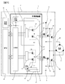
- FIG. 1 is a block diagram showing a configuration of an embodiment of a motor control device according to the present invention.
- the motor control device 1 in FIG. 1 is different from the motor control device 1 ′ in FIG. 7 in that a current cutoff circuit 23 is provided between the high-side push-pull circuit 19 and the booster circuit 5 of each phase, The difference is that a current cut-off circuit 38 is provided between the low-side push-pull circuit 34 and the power supply circuit 4.
- the U-phase pre-driver circuit 12 is shown as a representative example.
- current cutoff circuits 23 and 38 are respectively provided. Is provided.
- the feature of the present invention resides in that current interrupting circuits 23 and 38 are provided in each phase of the motor control device 1 as shown in FIG.
- the current interrupting circuits 23 and 38 of each phase are used when the semiconductor switch elements 20, 21, 35, or 36 of the pre-driver circuits 12 to 14 are short-circuited due to junction breakdown and a large current flows.
- the current flowing through the provided pre-driver circuit 12, 13 or 14 is cut off.
- the boosted voltage or power supply voltage supplied to the other two phases is not affected, and normal output is possible in the remaining two phases.
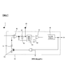
- FIG. 2 is a block diagram showing a configuration example of the current cutoff circuit 23 according to the first embodiment of the present invention.
- the current interrupt circuit 23 of this embodiment includes operational amplifiers 46 and 47, a filter circuit 48, a current detection resistor 50, a current limiting resistor 51, a switch element 54, and a current detection circuit 93.
- the current interrupt circuit 23 is shown here as a representative example, the current interrupt circuit 38 has a similar configuration.
- the operational amplifier 46 is provided between the boost voltage supply wiring 7 from the boost circuit 5 and the boost voltage output wiring 25 connected to the high side push-pull circuit 19.
- the operational amplifier 46 constitutes a voltage follower circuit for supplying the boosted voltage output from the booster circuit 5 to the high side push-pull circuit 19.
- the booster circuit 5 is connected to the power supply circuit 4 as shown in FIG. That is, a voltage follower circuit configured by the operational amplifier 46 is provided between the power supply circuit 4 and the high-side push-pull circuit 19 in the pre-driver circuit 12.
- an operational amplifier 46 is provided between the power supply wiring 6 from the power supply circuit 4 and the power supply output wiring 40 (see FIG. 1) connected to the low-side push-pull circuit 34. That is, a voltage follower circuit configured by the operational amplifier 46 is provided between the power supply circuit 4 and the low-side push-pull circuit 34 in the pre-driver circuit 12.
- the current detection circuit 93 detects the magnitude of the current 92 flowing through the current detection resistor 50 by the output voltage from the operational amplifier 46.
- the current detection circuit 93 outputs a current detection voltage corresponding to the detection value of the current 92 to the operational amplifier 47. This current detection voltage is input to the non-inverting input side of the operational amplifier 47.
- the operational amplifier 47 compares the current detection voltage from the current detection circuit 93 input to the non-inverting input side with the reference voltage 95 input to the inverting input side, and outputs a comparator output corresponding to the comparison result to the filter circuit 48. Output to. A logical sum of the comparator output that has passed through the filter circuit 48 and the arithmetic processing unit signal output from the arithmetic processing unit 10 is output to the gate terminal of the switch element 54 as a switch element drive signal.
- the comparator output that has passed through the filter circuit 48 is output to the logic circuit 11 as the failure diagnosis output 24.
- the occurrence of an abnormality can be detected by outputting the failure diagnosis output 24 from the current interrupt circuit 23.
- the failure diagnosis output 24 may be output to the arithmetic processing unit 10 instead of the logic circuit 11.
- the failure diagnosis output 24 may be output to both the logic circuit 11 and the arithmetic processing unit 10.
- the comparator output from the operational amplifier 47 that has passed through the filter circuit 48 is output to the logic circuit 11 as a failure diagnosis output 39 (see FIG. 1).
- the failure diagnosis output 39 may be output to the arithmetic processing device 10 instead of the logic circuit 11, or may be output to both the logic circuit 11 and the arithmetic processing device 10.
- the operation of the current interrupt circuit 23 will be described.
- the high-side push-pull circuit 19 When the high-side push-pull circuit 19 is normal, the current 92 flowing through the current detection resistor 50 is relatively small, so that the current detection voltage output from the current detection circuit 93 is less than the reference voltage 95. Therefore, the comparator output output from the operational amplifier 47 is at a low level, and the switch element 54 is turned off. As a result, the boosted voltage input from the booster circuit 5 to the voltage follower circuit of the operational amplifier 46 via the boosted voltage supply wiring 7 is output to the high side push-pull circuit 19 via the boosted voltage output wiring 25. Further, since the comparator output output from the operational amplifier 47 is at low level, the failure diagnosis output 24 is also at low level. That is, the high-level failure diagnosis output 24 indicating a failure is not output.
- the high-side push-pull circuit 19 for example, when the semiconductor switch element 20 is short-circuited, a through current flows from the booster circuit 5 to the ground via the boosted voltage supply wiring 7 as described above. This through current is detected by the current detection circuit 93 as a current 92 flowing through the current detection resistor 50. By detecting a through current of a predetermined value or more as the current 92, when the current detection voltage output from the current detection circuit 93 exceeds the reference voltage 95, the comparator output output from the operational amplifier 47 becomes high level. As a result, the switch element 54 is turned on, and a high-level failure diagnosis output 24 indicating a failure is output.
- the switch element 54 When the switch element 54 is turned on, the output voltage from the voltage follower circuit of the operational amplifier 46 changes and is fixed at the low level. As a result, the boosted voltage from the booster circuit 5 is blocked by the operational amplifier 46 and is not supplied to the high side push-pull circuit 19. Thereby, the current supply from the power supply circuit 4 to the pre-driver circuit 12 via the booster circuit 5 is cut off.
- the on / off of the switch element 54 can be controlled by the arithmetic processing unit signal output from the arithmetic processing unit 10. That is, the arithmetic processing unit 10 determines whether or not a predetermined current interruption condition is satisfied. When it is determined that the current interruption condition is satisfied, the arithmetic processing unit 10 outputs an arithmetic processing unit signal to the current interruption circuit 23. Thus, the current supply from the power supply circuit 4 to the pre-driver circuit 12 can be forcibly cut off. The same applies to the current interrupt circuit 38.
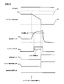
- FIG. 3 is a timing chart at the time of current interruption in the first embodiment of the present invention.
- the current 92 flowing through the current detection resistor 50 starts to increase, and the current detection output from the current detection circuit 93 increases as indicated by reference numeral 102.
- the boosted voltage output from the booster circuit 5 to the boosted voltage output wiring 25 of the pre-driver circuit 12 starts to decrease from the normal voltage 58 as indicated by reference numeral 101.
- the comparator output from the operational amplifier 47 changes from low level to high level as indicated by reference numeral 103.
- a predetermined filter time indicated by reference numeral 56 elapses from the rising edge of the comparator output, as shown by reference numerals 104 and 105, the failure diagnosis output 24 and the switch element drive signal output to the switch element 54 change from low level to high. Accordingly, the output voltage of the operational amplifier 46 is fixed to the low level.
- the boosted voltage output from the booster circuit 5 to the boosted voltage output wiring 25 of the predriver circuit 12 decreases to the voltage 59 at the time of abnormality as indicated by reference numeral 101, and the current supply to the predriver circuit 12 is cut off. Is done.
- the current interrupt circuit 23 can also reduce the adverse effect on the other two phases due to the junction breakdown of the semiconductor switch elements 35 and 36, and can continue to drive the motor stably even when an abnormality occurs.
- the motor control device 1 for controlling the three-phase motor 2 includes a high-side semiconductor switching element 27 to 29 and a low-side semiconductor provided for each phase of the three-phase motor 2 to drive the three-phase motor 2.
- Pre-driver circuits 12 to 14 provided for each phase of the three-phase motor 2 to control the operations of the switch elements 42 to 44, the high-side semiconductor switch elements 27 to 29, and the low-side semiconductor switch elements 42 to 44;
- the power supply circuit 4 that supplies current to the pre-driver circuits 12 to 14, the arithmetic processing device 10 that calculates and outputs a motor control signal, and the three-phase motor 2 based on the motor control signal output from the arithmetic processing device 10
- the logic circuit 11 that outputs the drive signal of each phase, and the operations of the pre-driver circuits 12 to 14 are controlled based on the drive signal output from the logic circuit 11.
- the pre-driver circuits 12 to 14 correspond to the high-side push-pull circuit 19 provided corresponding to the high-side semiconductor switch elements 27 to 29 of each phase and the low-side semiconductor switch elements 42 to 44 of each phase.
- the current cut-off circuits 23 and 38 are configured to cut off the supply of current to at least one of the high-side push-pull circuit 19 and the low-side push-pull circuit 34. did.
- the operations of the high-side semiconductor switch elements 27 to 29 and the low-side semiconductor switch elements 42 to 44 are appropriately controlled by the high-side push-pull circuit 19 and the low-side push-pull circuit 34, respectively.
- stable current driving can be continued by cutting off the current supply to the circuit.
- the current cut-off circuits 23 and 38 are the magnitude of the current supplied to the voltage follower circuit by the operational amplifier 46 and the predriver circuits 12 to 14 provided between the power supply circuit 4 and the predriver circuits 12 to 14.
- the output voltage of the voltage follower circuit by the operational amplifier 46 is changed to change from the power supply circuit 4 to the current detection circuit 93.
- the supply of current to the pre-driver circuits 12 to 14 was cut off. Thus, it is possible to reliably detect an abnormality occurring in the pre-driver circuits 12 to 14 and cut off the current supply.
- the current interrupting circuits 23 and 38 when the current supplied to the pre-driver circuits 12 to 14 is equal to or greater than a predetermined value, send a fault diagnosis signal 24, to at least one of the arithmetic processing unit 10 and the logic circuit 11, 39 was output.
- a fault diagnosis signal 24 to at least one of the arithmetic processing unit 10 and the logic circuit 11, 39 was output.
- the motor control device 1 includes the semiconductor device 3 in which a plurality of circuits including at least the pre-driver circuits 12 to 14, the logic circuit 11, the drive circuits 22 and 37, and the current cutoff circuits 23 and 38 are integrated. . Thereby, size reduction and cost reduction of the motor control apparatus 1 can be achieved.
- FIG. 4 is a block diagram showing a configuration example of the current interrupt circuit 23 according to the second embodiment of the present invention.
- the current cut-off circuit 23 according to the present embodiment is an alternative to the operational amplifier 46, the current detection resistor 50, the current limiting resistor 51, the switch element 54, and the current detection circuit 93, as compared with the one according to the first embodiment shown in FIG. 1 except that a diode 49 and an overcurrent cutoff fuse 57 are provided.
- the current interruption circuit 23 is shown here as a representative example, the current interruption circuit 38 has a similar configuration.
- the overcurrent cutoff fuse 57 is provided between the boosted voltage supply wiring 7 from the booster circuit 5 and the boosted voltage output wiring 25 connected to the high-side push-pull circuit 19 in the same manner as the operational amplifier 46 in FIG. That is, an overcurrent cutoff fuse 57 is provided between the power supply circuit 4 and the high-side push-pull circuit 19 in the pre-driver circuit 12. Similarly, in the current interrupt circuit 38, an overcurrent interrupt fuse 57 is provided between the power supply circuit 4 and the low-side push-pull circuit 34 in the pre-driver circuit 12.
- the operational amplifier 47 compares the output side voltage of the overcurrent cutoff fuse 57 input to the non-inverting input side with the input side voltage of the overcurrent cutoff fuse 57 input to the inverting input side via the diode 49.
- the comparator output corresponding to the comparison result is output to the filter circuit 48.
- This comparator output is inverted and passes through the filter circuit 48 and then output to the logic circuit 11 as a failure diagnosis output 24.
- the failure diagnosis output 24 may be output to the arithmetic processing unit 10 instead of the logical circuit 11, or the logical circuit 11 and the arithmetic processing unit 10. You may output to both. This also applies to the failure diagnosis output 39 output from the current interrupt circuit 38.
- the overcurrent breaking fuse 57 When the high-side push-pull circuit 19 is normal, the current flowing through the overcurrent breaking fuse 57 is relatively small, so the overcurrent breaking fuse 57 is not blown. Therefore, the boosted voltage input from the booster circuit 5 through the boosted voltage supply wiring 7 is output to the high side push-pull circuit 19 through the overcurrent cutoff fuse 57 and the boosted voltage output wiring 25. Further, since the voltage on the non-inverting input side of the operational amplifier 47 is higher than the voltage on the inverting input side by the drop voltage of the diode 49, the comparator output from the operational amplifier 47 becomes high level. Therefore, the failure diagnosis output 24 obtained by inverting the comparator output is not output at a low level.
- the high-side push-pull circuit 19 for example, when the semiconductor switch element 20 is short-circuited, a relatively large through current flows from the booster circuit 5 to the ground via the boosted voltage supply wiring 7.
- the overcurrent cutoff fuse 57 is blown to cut off the boosted voltage from the booster circuit 5 and is not supplied to the high side push-pull circuit 19. Thereby, the current supply from the power supply circuit 4 to the pre-driver circuit 12 via the booster circuit 5 is cut off.
- the failure diagnosis output 24 obtained by inverting the comparator output is output at a high level.
- the current interruption circuits 23 and 38 include an overcurrent interruption fuse 57 provided between the power supply circuit 4 and the predriver circuits 12 to 14, and the magnitude of the current supplied to the predriver circuits 12 to 14
- the overcurrent cutoff fuse 57 is blown to cut off the supply of current from the power supply circuit 4 to the pre-driver circuits 12-14.
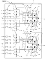
- FIG. 5 is a block diagram showing a configuration example of the pre-driver circuit 12 according to the third embodiment of the present invention.
- the pre-driver circuit 12 according to the present embodiment divides the high-side push-pull circuit 19 and the low-side push-pull circuit 34 into a plurality of push-pull circuits, respectively, as compared with the one according to the first embodiment shown in FIG. The point is mainly different. That is, the high-side push-pull circuit 19 includes a push-pull circuit composed of semiconductor switch elements 62 and 65, a push-pull circuit composed of semiconductor switch elements 63 and 66, and semiconductor switch elements 64 and 67. The push-pull circuit is connected in parallel to the power supply circuit 4 via the boost voltage supply wiring 7 and the boost circuit 5.
- the low-side push-pull circuit 34 includes a push-pull circuit composed of semiconductor switch elements 77 and 80, a push-pull circuit composed of semiconductor switch elements 78 and 81, and semiconductor switch elements 79 and 82.
- the push-pull circuit is connected in parallel to the power supply circuit 4 via the power supply wiring 6.
- an example is shown in which three push-pull circuits are connected in parallel in the high-side push-pull circuit 19 and the low-side push-pull circuit 34, but the columns of push-pull circuits in parallel are not limited to this.
- the U-phase pre-driver circuit 12 is shown here as a representative example, the other V-phase and W-phase pre-driver circuits 13 and 14 have the same configuration.
- Each push-pull circuit constituting the high-side push-pull circuit 19 has a current cutoff circuit similar to the current cutoff circuit 23 according to the second embodiment shown in FIG. 4 on the boost voltage supply wiring 7 side and the ground side. Each is connected. That is, the operational amplifier 47, the filter circuit 48, and the overcurrent cutoff fuse 57 are connected to the boosted voltage supply wiring 7 side and the ground side of each push-pull circuit, respectively.
- each push-pull circuit constituting the low-side push-pull circuit 34 includes an operational amplifier 47, a filter circuit 48, and an overcurrent cutoff fuse 57 on the power supply wiring 6 side and the ground side of each push-pull circuit, respectively. It is connected.
- the operational amplifiers 47 on the boosted voltage supply wiring 7 side of the high side push-pull circuit 19 and the operational amplifiers 47 on the power supply wiring 6 side of the low side push-pull circuit 34 are for overcurrent blocking input to the non-inverting input side.
- These comparator outputs are inverted as in the second embodiment, pass through each filter circuit 48, and then output to the logic circuit 11 as fault diagnosis outputs 71 to 73 and 86 to 88, respectively.
- each operational amplifier 47 on the ground side of the high-side push-pull circuit 19 and the low-side push-pull circuit 34 has an input-side voltage (semiconductor switch elements 65 to 67 or semiconductor switch elements 65 to 67 or The source terminal voltages 80 to 82 are compared with a predetermined reference voltage 70 or 85 input to the inverting input side, and a comparator output corresponding to the comparison result is output to the filter circuit 48, respectively. These comparator outputs are inverted and pass through the filter circuits 48, and are output to the logic circuit 11 as fault diagnosis outputs 74 to 76 and 89 to 91, respectively.
- each failure diagnosis output described above may be output to the arithmetic processing unit 10 instead of the logical circuit 11, or the logical circuit 11 and the arithmetic processing unit. 10 may be output to both.
- semiconductor switch elements 62 to 64 have variations in individual on-resistance values due to manufacturing variations and wiring parasitic resistance.
- a large amount of current flows through the semiconductor switch elements 62 to 64 having the smallest on-resistance value a difference occurs in the occurrence state of the short circuit failure in the semiconductor switch elements 62 to 64.
- the semiconductor switch element 62 is short-circuited first.
- the operational amplifier 47 connected to the push-pull circuit has a higher voltage than the non-inverting input side voltage.
- the voltage on the inverting input side becomes higher, and the comparator output becomes low level.
- the failure diagnosis output 71 is output at a high level.
- FIG. 6 is a timing chart at the time of current interruption in the third embodiment of the present invention.
- the drive signal (control signal) input from the logic circuit 11 to the pre-driver circuit 12 changes from the low level to the high level as indicated by reference numeral 106
- the high-side semiconductor switch from the pre-driver circuit 12 through the pre-driver output wiring 26.
- the predriver output voltage output to the gate terminal of the element 27 rises to the normal voltage 60 as indicated by reference numeral 107.
- the comparator output from the operational amplifier 47 changes from the high level to the low level as indicated by reference numeral 109.
- the failure diagnosis output 71 changes from low level to high level as indicated by reference numeral 110 and is output to the logic circuit 11.
- the pre-driver circuits 12 to 14 include a plurality of push-pull circuits connected in parallel to the power supply circuit 4 for each phase of the three-phase motor 2, and include an operational amplifier 47, a filter circuit 48, and an overcurrent cutoff circuit.
- the current cut-off circuit constituted by the fuse 57 cuts off the supply of current from the power supply circuit 4 to at least one of the plurality of push-pull circuits.
Landscapes
- Engineering & Computer Science (AREA)
- Power Engineering (AREA)
- Control Of Motors That Do Not Use Commutators (AREA)
Abstract
モータ制御装置は、三相モータを駆動するために三相モータの各相ごとに設けられた半導体スイッチ素子と、半導体スイッチ素子の動作を制御するために三相モータの各相ごとに設けられたプリドライバ回路と、プリドライバ回路へ電流を供給する電源回路と、モータ制御信号を演算して出力する演算処理装置と、モータ制御信号に基づいて三相モータの各相の駆動信号を出力する論理回路と、駆動信号に基づいてプリドライバ回路の動作を制御する駆動回路と、電流が所定値以上であるときに、電源回路からプリドライバ回路への電流の供給を遮断する電流遮断回路とを備える。
Description
本発明は、主に車載用の電動パワーステアリング装置、電動ウォーターポンプ装置、電動オイルポンプ装置、インバータ装置等に使用する三相モータを制御するためのモータ制御装置に関する。特に、異常が発生した場合においても安定したモータ駆動を続けることができるモータ制御装置に関する。
近年、地球環境保全、エネルギー有効利用及び安全性能向上の観点から、車両の重量軽減による燃費の向上等を目的として、従来の油圧によるパワーアシスト装置の代わりに、モータを用いてトルクアシストを行う電動パワーステアリング装置(EPS)が導入されている。電動パワーステアリング装置は、従来の油圧パワーステアリング装置のように常に油圧ポンプを回す必要がなく、必要なときだけモータを回して駆動力をアシストする。そのため、燃費の改善に効果がある。例えば、電動パワーステアリング装置のアシスト用モータには、比較的俊敏で高トルクを発生でき、制御が容易な三相ブラシレスDCモータが用いられている。
上記のようなモータの駆動を制御するためのモータ制御装置では、直流電力からモータの駆動電力を発生させるために半導体スイッチ素子が一般に用いられている。こうしたモータ制御装置において、外部要因により発生する誘導ノイズや過渡サージ等の外乱は、半導体スイッチ素子の故障を招くおそれがある。そこで、半導体スイッチ素子の故障を検出するための様々な技術が知られている。
例えば、特許文献1には、三相ブラシレスDCモータの駆動回路において、次のような技術が開示されている。すなわち、モータの各相の出力電圧を検出し、いずれか一相の電圧が所望の電圧を満たさない場合は半導体スイッチ素子の異常であると判断する。そして、三相駆動回路の供給電源を遮断させる。また、特許文献2には、三相交流モータ駆動用のインバータ回路において、次のような技術が開示されている。すなわち、駆動対象のモータの各相について、インバータ回路内の電源側(ハイサイド)とグランド側(ロウサイド)に半導体スイッチ素子とヒューズをそれぞれ設ける。ヒューズが溶断されたことを故障診断装置により検知することで各相の半導体スイッチ素子の故障を検出する。そして、二相駆動によりモータを応急運転する。
特許文献1に記載された技術では、いずれか一相の半導体スイッチ素子の異常が検出された場合、三相全ての駆動回路の供給電源が遮断される。そのため、それ以上モータ駆動を続けることができない。また、特許文献2に記載された技術では、モータ駆動用の半導体スイッチ素子に対して直列にヒューズが接続される。そのため、許容電流が大きなヒューズを使用する必要があり、コストアップにつながる。
本発明の第1の態様によるモータ制御装置は、三相モータを制御するためのものであって、三相モータを駆動するために三相モータの各相ごとに設けられた半導体スイッチ素子と、半導体スイッチ素子の動作を制御するために三相モータの各相ごとに設けられたプリドライバ回路と、プリドライバ回路へ電流を供給する電源回路と、モータ制御信号を演算して出力する演算処理装置と、演算処理装置から出力されたモータ制御信号に基づいて、三相モータの各相の駆動信号を出力する論理回路と、論理回路から出力された駆動信号に基づいて、プリドライバ回路の動作を制御する駆動回路と、電流が所定値以上であるときに、電源回路からプリドライバ回路への電流の供給を遮断する電流遮断回路とを備える。
本発明の第2の態様によると、第1の態様のモータ制御装置において、半導体スイッチ素子は、各相の高電圧側に設けられたハイサイド半導体スイッチ素子と、各相の低電圧側に設けられたロウサイド半導体スイッチ素子とを含むことが好ましい。また、プリドライバ回路は、各相のハイサイド半導体スイッチ素子に対応して設けられたハイサイドプッシュプル回路と、各相のロウサイド半導体スイッチ素子に対応して設けられたロウサイドプッシュプル回路とを含むことが好ましい。さらに、電流遮断回路は、ハイサイドプッシュプル回路およびロウサイドプッシュプル回路のいずれか少なくとも一方への電流の供給を遮断することが好ましい。
本発明の第3の態様によると、第1または第2の態様のモータ制御装置において、電流遮断回路は、電源回路とプリドライバ回路との間に設けられた電圧フォロワ回路と、電流の大きさを検出する電流検出回路とを含んでもよい。電流検出回路により検出された電流の大きさが所定値以上である場合、電圧フォロワ回路の出力電圧を変化させることにより、電源回路からプリドライバ回路への電流の供給を遮断することが好ましい。
本発明の第4の態様によると、第1または第2の態様のモータ制御装置において、電流遮断回路は、電源回路とプリドライバ回路との間に設けられた過電流遮断用ヒューズを含んでもよい。電流の大きさが所定値以上である場合、過電流遮断用ヒューズが溶断することにより、電源回路からプリドライバ回路への電流の供給を遮断することが好ましい。
本発明の第5の態様によると、第1または第2の態様のモータ制御装置において、プリドライバ回路は、三相モータの各相ごとに電源回路に対して並列に接続された複数のプッシュプル回路を含んでもよい。電流遮断回路は、電源回路から複数のプッシュプル回路のいずれか少なくとも1つへの電流の供給を遮断することが好ましい。
本発明の第6の態様によると、第1~第5いずれかの態様のモータ制御装置において、電流遮断回路は、電流が所定値以上であるときに、演算処理装置または論理回路のいずれか少なくとも一方へ故障診断信号を出力することが好ましい。
本発明の第7の態様によると、第1~第6いずれかの態様のモータ制御装置は、プリドライバ回路、論理回路、駆動回路および電流遮断回路を少なくとも含む複数の回路を集積化した半導体装置を有してもよい。
本発明によれば、異常が発生した場合においても安定したモータ駆動を続けることができるモータ制御装置を低コストで提供することができる。
(従来技術の説明)
以下に本発明の実施の形態について説明する。最初に、図7を用いて本発明の従来技術についての説明を行う。図7は、従来技術によるモータ制御装置の構成例を示すブロック図である。
以下に本発明の実施の形態について説明する。最初に、図7を用いて本発明の従来技術についての説明を行う。図7は、従来技術によるモータ制御装置の構成例を示すブロック図である。
図7に示すモータ制御装置1´は、三相モータ2の駆動を制御するためのものであり、半導体装置3、電源回路4および演算処理装置(MPU)10と、バッテリ電圧8とグランド9の間にそれぞれ接続されたモータ駆動用のハイサイド半導体スイッチ素子27~29およびロウサイド半導体スイッチ素子42~44とを有する。
半導体装置3は、昇圧回路5および論理回路11と、三相モータ2のU相、V相およびW相の各相にそれぞれ対応するプリドライバ回路12~14とを有している。これらの各回路は、半導体装置3において集積化されており、一体化された集積回路としての半導体装置3を構成している。
プリドライバ回路12~14の各々は、ハイサイド半導体スイッチ素子27~29に対応するハイサイドプッシュプル回路19を構成する半導体スイッチ素子20および21と、ロウサイド半導体スイッチ素子42~44に対応するロウサイドプッシュプル回路34を構成する半導体スイッチ素子35および36と、これらのプッシュプル回路19、34の動作をそれぞれ制御する駆動回路22、37とを有する。なお、図7では各相のプリドライバ回路12~14を代表してU相のプリドライバ回路12の構成を図示しているが、他のV相、W相のプリドライバ回路13、14も同様の構成を有している。したがって、以下では、各相のプリドライバ回路12~14を代表して、U相のプリドライバ回路12の動作を中心に説明を行うこととする。
電源回路4は、所定の電源電圧を生成して半導体装置3へ出力する。半導体装置3において入力された電源電圧は、電源供給配線6を介して昇圧回路5およびプリドライバ回路12のロウサイドプッシュプル回路34へ供給される。昇圧回路5は、電源回路4から電源供給配線6を介して供給された電源電圧を昇圧し、電源電圧よりも高い昇圧電圧を昇圧電圧供給配線7を介してプリドライバ回路12のハイサイドプッシュプル回路19へ供給する。これは、ハイサイド半導体スイッチ素子27をオンするためにハイサイドプッシュプル回路19からハイサイド半導体スイッチ素子27へ出力するゲート-ソース間電圧は、U相のモータ出力配線45におけるモータ駆動出力の電圧レベルよりも高くする必要があるためである。プリドライバ回路12では、こうして電源回路4から供給された電源電圧およびそれを昇圧した昇圧電圧によって電流が流れる。これにより、電源回路4からプリドライバ回路12への電流供給が行われる。
演算処理装置10は、モータ2の回転状態や外部からの指令に基づいてモータ制御信号を演算し、論理回路11へ出力する。論理回路11は、演算処理装置10から出力されたモータ制御信号に基づいて、プリドライバ回路12の動作を制御するための駆動信号を生成し、プリドライバ回路12へ出力する。
プリドライバ回路12では、論理回路11から出力された駆動信号に基づいて、駆動回路22、37により、ハイサイドプッシュプル回路19の動作とロウサイドプッシュプル回路34の動作をそれぞれ制御する。駆動回路22は、駆動信号に応じてハイサイドプッシュプル回路19の半導体スイッチ素子20または21のいずれか一方をオンさせる。これにより、プリドライバ回路12からプリドライバ出力配線26を介して、昇圧電圧またはグランド電圧がハイサイド半導体スイッチ素子27のゲート端子へ出力され、ハイサイド半導体スイッチ素子27の動作が制御される。
駆動回路37も駆動回路22と同様に、駆動信号に応じてロウサイドプッシュプル回路34の半導体スイッチ素子35または36のいずれか一方をオンさせる。これにより、プリドライバ回路12からプリドライバ出力配線41を介して、電源電圧またはグランド電圧がロウサイド半導体スイッチ素子42のゲート端子へ出力され、ロウサイド半導体スイッチ素子42の動作が制御される。
ここで、モータ制御装置1´の故障発生原因について説明する。モータ制御装置1´は、例えば車両に搭載される電動パワーステアリング装置などにおいて使用される。その場合、操舵補助力をモータ2から出力する際などに、外部要因の影響により誘導ノイズや過渡サージ等の外乱が生じることがある。これらの外乱は、ハイサイド半導体スイッチ素子27~29やロウサイド半導体スイッチ素子42~44のドレイン-ソース間またはゲート-ソース間における接合破壊を引き起こし、短絡故障の原因となり得る。
上記のような短絡故障がハイサイド半導体スイッチ素子27~29またはロウサイド半導体スイッチ素子42~44において発生すると、当該スイッチ素子に対応して設けられたハイサイドプッシュプル回路19の半導体スイッチ素子20、21またはロウサイドプッシュプル回路34の半導体スイッチ素子35、36の接合破壊を誘発し、短絡故障を引き起こすおそれがある。例えば、U相のプリドライバ回路12において半導体スイッチ素子20が短絡故障を起こした状態で半導体スイッチ素子21がオンされると、昇圧回路5から昇圧電圧供給配線7を介してグランドへ貫通電流が流れる。この場合の貫通電流は大電流であるため、回路故障を招くおそれがある。
また、例えばU相のプリドライバ回路12においてハイサイドプッシュプル回路19の半導体スイッチ素子20がある程度の抵抗値を持った状態で短絡故障をした場合、常に半導体スイッチ素子20において貫通電流が流れることになるため、昇圧回路5から供給される昇圧電圧の低下を引き起こす。近年の車載機器では機能安全に関する規制が厳しくなる傾向にあるため、半導体スイッチ素子20が短絡故障を起こした場合でも、モータ制御装置1´に対して要求される最低限のシステム性能を成立させなくてはならない。そこで、短絡故障時に最低限のモータ駆動補償を実現するために、モータ制御装置1´では、短絡故障が起きていない他の二相(ここではV相およびW相)を用いた二相駆動によりモータ2を駆動することができるようにしている。しかし、上記のような昇圧電圧の低下は、二相駆動によるモータ2の駆動に悪影響を及ぼすことになる。これは、ロウサイドプッシュプル回路34の半導体スイッチ素子35が短絡故障した場合に電源回路4から供給される電源電圧においても同様である。
そこで本発明では、上述のプリドライバ回路12~14における半導体スイッチ素子20、21または半導体スイッチ素子35、36の接合破壊による他の二相への悪影響を低減させ、安定したモータ駆動を続けることができるようにすることを目的の一つとする。なお、この目的を実現するための方法の一つとして、各相ごとに電源回路4を設けることも考えられるが、これは装置全体のコストアップを招くために現実的ではない。したがって、上記目的を低コストで実現できることをさらに目的の一つとする。
(本発明の説明)
図1は、本発明によるモータ制御装置の一実施形態の構成を示すブロック図である。図1のモータ制御装置1は、図7のモータ制御装置1´と比較して、各相のハイサイドプッシュプル回路19と昇圧回路5の間に電流遮断回路23を設けた点と、各相のロウサイドプッシュプル回路34と電源回路4の間に電流遮断回路38を設けた点とが異なっている。なお、図1ではU相のプリドライバ回路12を代表例として図示しているが、V相のプリドライバ回路13およびW相のプリドライバ回路14においても同様に、電流遮断回路23および38がそれぞれ設けられている。
図1は、本発明によるモータ制御装置の一実施形態の構成を示すブロック図である。図1のモータ制御装置1は、図7のモータ制御装置1´と比較して、各相のハイサイドプッシュプル回路19と昇圧回路5の間に電流遮断回路23を設けた点と、各相のロウサイドプッシュプル回路34と電源回路4の間に電流遮断回路38を設けた点とが異なっている。なお、図1ではU相のプリドライバ回路12を代表例として図示しているが、V相のプリドライバ回路13およびW相のプリドライバ回路14においても同様に、電流遮断回路23および38がそれぞれ設けられている。
本発明の特徴は、図1に示すように、モータ制御装置1の各相に電流遮断回路23および38を設けたことにある。各相の電流遮断回路23および38は、プリドライバ回路12~14の半導体スイッチ素子20、21、35または36が接合破壊のために短絡故障して大電流が流れたときに、当該スイッチ素子が設けられたプリドライバ回路12、13または14に流れる電流を遮断する。これにより、大電流による回路故障を防ぐと共に、昇圧回路5から出力される昇圧電圧または電源回路4から供給される電源電圧の低下を防ぐことができる。その結果、他の二相に供給される昇圧電圧または電源電圧には影響がないため、残り二相では正常出力が可能となる。
以下、図1の電流遮断回路23、38の実施形態について、図2~図6を参照して詳細に説明する。
(第1の実施の形態)
本発明の第1の実施の形態による電流遮断回路23、38の構成について、図2と図3を使用して説明する。
本発明の第1の実施の形態による電流遮断回路23、38の構成について、図2と図3を使用して説明する。
図2は、本発明の第1の実施の形態による電流遮断回路23の構成例を示すブロック図である。図2に示すように、本実施形態の電流遮断回路23は、オペアンプ46および47、フィルタ回路48、電流検出抵抗50、電流制限抵抗51、スイッチ素子54および電流検出回路93を有している。なお、ここでは電流遮断回路23を代表例として示しているが、電流遮断回路38も同様の構成を有している。
オペアンプ46は、昇圧回路5からの昇圧電圧供給配線7とハイサイドプッシュプル回路19に繋がる昇圧電圧出力配線25との間に設けられている。このオペアンプ46により、昇圧回路5から出力された昇圧電圧をハイサイドプッシュプル回路19へ供給するための電圧フォロワ回路が構成される。なお、昇圧回路5は、図1に示すように電源回路4と接続されている。すなわち、電源回路4とプリドライバ回路12内のハイサイドプッシュプル回路19との間に、オペアンプ46によって構成された電圧フォロワ回路が設けられている。
なお、電流遮断回路38でも同様に、電源回路4からの電源供給配線6とロウサイドプッシュプル回路34に繋がる電源出力配線40(図1参照)との間にオペアンプ46が設けられている。すなわち、電源回路4とプリドライバ回路12内のロウサイドプッシュプル回路34との間に、オペアンプ46によって構成された電圧フォロワ回路が設けられている。
ここで図2に戻って電流遮断回路23の説明を続ける。図2において、オペアンプ46からの出力電圧により電流検出抵抗50を流れる電流92の大きさは、電流検出回路93により検出される。電流検出回路93は、電流92の検出値に応じた電流検出電圧をオペアンプ47へ出力する。この電流検出電圧は、オペアンプ47の非反転入力側に入力される。
オペアンプ47は、非反転入力側に入力された電流検出回路93からの電流検出電圧と、反転入力側に入力される基準電圧95とを比較し、その比較結果に応じたコンパレータ出力をフィルタ回路48へ出力する。フィルタ回路48を通過したコンパレータ出力と演算処理装置10から出力された演算処理装置信号との論理和が、スイッチ素子54のゲート端子へスイッチ素子駆動信号として出力される。
また、フィルタ回路48を通過したコンパレータ出力は、故障診断出力24として論理回路11へ出力される。論理回路11では、電流遮断回路23から故障診断出力24が出力されることにより、異常の発生を検知することができる。なお、故障診断出力24を論理回路11ではなく演算処理装置10へ出力するようにしてもよい。あるいは、論理回路11と演算処理装置10の両方へ故障診断出力24を出力してもよい。
なお、電流遮断回路38では、フィルタ回路48を通過したオペアンプ47からのコンパレータ出力は、故障診断出力39(図1参照)として論理回路11へ出力される。この故障診断出力39も故障診断出力24と同様に、論理回路11ではなく演算処理装置10へ出力してもよいし、論理回路11と演算処理装置10の両方へ出力してもよい。
次に電流遮断回路23の動作を説明する。ハイサイドプッシュプル回路19が正常である場合、電流検出抵抗50に流れる電流92は比較的小さいため、電流検出回路93から出力される電流検出電圧は基準電圧95未満となる。そのため、オペアンプ47から出力されるコンパレータ出力はロウレベルとなり、スイッチ素子54はオフ状態となる。これにより、昇圧回路5から昇圧電圧供給配線7を介してオペアンプ46の電圧フォロワ回路へ入力された昇圧電圧が昇圧電圧出力配線25を介してハイサイドプッシュプル回路19へ出力される。また、オペアンプ47から出力されるコンパレータ出力がロウレベルであるため、故障診断出力24もロウレベルとなる。すなわち、故障を示すハイレベルの故障診断出力24は出力されない。
一方、ハイサイドプッシュプル回路19において、例えば半導体スイッチ素子20が短絡故障した場合、前述のように昇圧回路5から昇圧電圧供給配線7を介してグランドへ貫通電流が流れる。この貫通電流は、電流検出回路93において、電流検出抵抗50に流れる電流92として検出される。所定値以上の貫通電流を電流92として検出することにより、電流検出回路93から出力される電流検出電圧が基準電圧95を超えると、オペアンプ47から出力されるコンパレータ出力がハイレベルとなる。これにより、スイッチ素子54がオン状態になると共に、故障を示すハイレベルの故障診断出力24が出力される。
スイッチ素子54がオンすると、オペアンプ46の電圧フォロワ回路からの出力電圧が変化し、ロウレベルに固定される。その結果、昇圧回路5からの昇圧電圧はオペアンプ46において遮断され、ハイサイドプッシュプル回路19へ供給されなくなる。これにより、昇圧回路5を介した電源回路4からプリドライバ回路12への電流供給が遮断される。
なお、電流遮断回路38でも同様に、所定値以上の貫通電流を検出することにより電流検出回路93から出力される電流検出電圧が基準電圧95を超えると、故障を示すハイレベルの故障診断出力39が出力される。すると、スイッチ素子54がオン状態となり、オペアンプ46の電圧フォロワ回路からの出力電圧がロウレベルに固定される。その結果、電源回路4からの電源電圧がオペアンプ46において遮断されてロウサイドプッシュプル回路34へ供給されなくなる。これにより、電源回路4からプリドライバ回路12への電流供給が遮断される。
また、電流遮断回路23では、半導体スイッチ素子20の短絡故障が発生していない場合に、演算処理装置10から出力される演算処理装置信号によってスイッチ素子54のオンオフを制御することもできる。すなわち、予め定められた電流遮断条件を満たすか否かを演算処理装置10において判断し、電流遮断条件を満たすと判断した場合は演算処理装置10から電流遮断回路23へ演算処理装置信号を出力することで、電源回路4からプリドライバ回路12への電流供給を強制的に遮断することができる。これは、電流遮断回路38においても同様である。
図3は、本発明の第1の実施の形態における電流遮断時のタイミングチャートである。ハイサイドプッシュプル回路19において半導体スイッチ素子20の故障が発生すると、電流検出抵抗50に流れる電流92が上昇し始めることにより、電流検出回路93からの電流検出出力が符号102に示すように上昇する。また、これと同時に、昇圧回路5からプリドライバ回路12の昇圧電圧出力配線25へ出力される昇圧電圧は、符号101に示すように、正常時の電圧58から低下し始める。
電流検出回路93からの電流検出出力が基準電圧95に達すると、オペアンプ47からのコンパレータ出力は、符号103に示すようにロウレベルからハイレベルへと変化する。このコンパレータ出力の立上りエッジから符号56に示す所定のフィルタ時間が経過すると、符号104および105に示すように、故障診断出力24と、スイッチ素子54へ出力されるスイッチ素子駆動信号とがロウレベルからハイレベルへと変化し、それに応じて、オペアンプ46の出力電圧がロウレベルに固定される。その結果、昇圧回路5からプリドライバ回路12の昇圧電圧出力配線25へ出力される昇圧電圧が、符号101に示すように異常時の電圧59まで低下し、プリドライバ回路12への電流供給が遮断される。
以上説明したようにして、電流遮断回路23により短絡故障時の貫通電流を遮断することにより、プリドライバ回路12における半導体スイッチ素子20、21の接合破壊による他の二相への悪影響を低減させることができる。その結果、異常が発生した場合においても安定したモータ駆動を続けることができる。なお、電流遮断回路38でも同様に、半導体スイッチ素子35、36の接合破壊による他の二相への悪影響を低減させ、異常が発生した場合においても安定したモータ駆動を続けることができる。さらに、U相以外の二相、すなわちV相およびW相についても同様である。
以上説明した本発明の第1の実施の形態によれば、次の作用効果を奏する。
(1)三相モータ2を制御するためのモータ制御装置1は、三相モータ2を駆動するために三相モータ2の各相ごとに設けられたハイサイド半導体スイッチ素子27~29およびロウサイド半導体スイッチ素子42~44と、ハイサイド半導体スイッチ素子27~29およびロウサイド半導体スイッチ素子42~44の動作を制御するために三相モータ2の各相ごとに設けられたプリドライバ回路12~14と、プリドライバ回路12~14へ電流を供給する電源回路4と、モータ制御信号を演算して出力する演算処理装置10と、演算処理装置10から出力されたモータ制御信号に基づいて三相モータ2の各相の駆動信号を出力する論理回路11と、論理回路11から出力された駆動信号に基づいてプリドライバ回路12~14の動作を制御する駆動回路22、37と、上記電流が所定値以上であるときに電源回路4からプリドライバ回路12~14への電流の供給を遮断する電流遮断回路23、38とを備える。このようにしたので、異常が発生した場合においても安定したモータ駆動を続けることができるモータ制御装置1を低コストで提供することができる。
(2)プリドライバ回路12~14は、各相のハイサイド半導体スイッチ素子27~29に対応して設けられたハイサイドプッシュプル回路19と、各相のロウサイド半導体スイッチ素子42~44に対応して設けられたロウサイドプッシュプル回路34とを含み、電流遮断回路23、38は、ハイサイドプッシュプル回路19およびロウサイドプッシュプル回路34のいずれか少なくとも一方への電流の供給を遮断するようにした。これにより、ハイサイド半導体スイッチ素子27~29およびロウサイド半導体スイッチ素子42~44の動作をハイサイドプッシュプル回路19およびロウサイドプッシュプル回路34によりそれぞれ適切に制御しつつ、ハイサイドプッシュプル回路19およびロウサイドプッシュプル回路34のいずれか少なくとも一方に異常が発生した場合は、その回路への電流供給を遮断して安定したモータ駆動を続けることができる。
(3)電流遮断回路23、38は、電源回路4とプリドライバ回路12~14との間に設けられたオペアンプ46による電圧フォロワ回路と、プリドライバ回路12~14へ供給される電流の大きさを検出する電流検出回路93とを含み、電流検出回路93により検出された電流の大きさが所定値以上である場合、オペアンプ46による電圧フォロワ回路の出力電圧を変化させることにより、電源回路4からプリドライバ回路12~14への電流の供給を遮断するようにした。これにより、プリドライバ回路12~14において発生した異常を確実に検知して電流供給を遮断することができる。
(4)電流遮断回路23、38は、プリドライバ回路12~14へ供給される電流が所定値以上であるときに、演算処理装置10または論理回路11のいずれか少なくとも一方へ故障診断信号24、39をそれぞれ出力するようにした。これにより、プリドライバ回路12~14において異常が発生したことをモータ制御装置1のシステム全体で把握し、必要に応じてユーザへの警告等の措置を講じることができる。
(5)モータ制御装置1は、プリドライバ回路12~14、論理回路11、駆動回路22、37および電流遮断回路23、38を少なくとも含む複数の回路を集積化した半導体装置3を有することとした。これにより、モータ制御装置1の小型化および低コスト化を図ることができる。
(第2の実施の形態)
本発明の第2の実施の形態による電流遮断回路23、38の構成について、図4を使用して説明する。
本発明の第2の実施の形態による電流遮断回路23、38の構成について、図4を使用して説明する。
図4は、本発明の第2の実施の形態による電流遮断回路23の構成例を示すブロック図である。本実施形態による電流遮断回路23は、図2に示した第1の実施の形態によるものと比べて、オペアンプ46、電流検出抵抗50、電流制限抵抗51、スイッチ素子54および電流検出回路93の代わりに、ダイオード49および過電流遮断用ヒューズ57を有する点が異なっている。なお、ここでは電流遮断回路23を代表例として示しているが、電流遮断回路38も同様の構成を有している。
過電流遮断用ヒューズ57は、図2のオペアンプ46と同様に、昇圧回路5からの昇圧電圧供給配線7とハイサイドプッシュプル回路19に繋がる昇圧電圧出力配線25との間に設けられている。すなわち、電源回路4とプリドライバ回路12内のハイサイドプッシュプル回路19との間に過電流遮断用ヒューズ57が設けられている。なお、電流遮断回路38でも同様に、電源回路4とプリドライバ回路12内のロウサイドプッシュプル回路34との間に過電流遮断用ヒューズ57が設けられている。
オペアンプ47は、非反転入力側に入力される過電流遮断用ヒューズ57の出力側電圧と、ダイオード49を介して反転入力側に入力される過電流遮断用ヒューズ57の入力側電圧とを比較し、その比較結果に応じたコンパレータ出力をフィルタ回路48へ出力する。このコンパレータ出力は、反転されてフィルタ回路48を通過した後、故障診断出力24として論理回路11へ出力される。なお、先に説明した第1の実施の形態の場合と同様に、故障診断出力24を論理回路11ではなく演算処理装置10へ出力するようにしてもよいし、論理回路11と演算処理装置10の両方へ出力してもよい。この点は、電流遮断回路38から出力される故障診断出力39についても同様である。
ハイサイドプッシュプル回路19が正常である場合、過電流遮断用ヒューズ57に流れる電流は比較的小さいため、過電流遮断用ヒューズ57は溶断しない。そのため、昇圧回路5から昇圧電圧供給配線7を介して入力された昇圧電圧が過電流遮断用ヒューズ57および昇圧電圧出力配線25を介してハイサイドプッシュプル回路19へ出力される。また、オペアンプ47の非反転入力側の電圧は、反転入力側の電圧よりもダイオード49のドロップ電圧分だけ高いため、オペアンプ47からのコンパレータ出力はハイレベルとなる。そのため、コンパレータ出力を反転した故障診断出力24はロウレベルとなって出力されない。
一方、ハイサイドプッシュプル回路19において、例えば半導体スイッチ素子20が短絡故障した場合、昇圧回路5から昇圧電圧供給配線7を介してグランドへ比較的大きな貫通電流が流れる。所定値以上の貫通電流が流れると、過電流遮断用ヒューズ57が溶断されることにより昇圧回路5からの昇圧電圧が遮断され、ハイサイドプッシュプル回路19へ供給されなくなる。これにより、昇圧回路5を介した電源回路4からプリドライバ回路12への電流供給が遮断される。また、昇圧回路5からの昇圧電圧が遮断されることにより、オペアンプ47の非反転入力側の電圧よりも反転入力側の電圧の方が高くなり、オペアンプ47からのコンパレータ出力がロウレベルとなる。そのため、コンパレータ出力を反転した故障診断出力24がハイレベルとなって出力される。
以上説明した本発明の第2の実施の形態によれば、第1の実施の形態で説明した(1)、(2)、(4)および(5)の各作用効果に加えて、さらに次の(6)のような作用効果を奏する。
(6)電流遮断回路23、38は、電源回路4とプリドライバ回路12~14との間に設けられた過電流遮断用ヒューズ57を含み、プリドライバ回路12~14へ供給される電流の大きさが所定値以上である場合、過電流遮断用ヒューズ57が溶断することにより、電源回路4からプリドライバ回路12~14への電流の供給を遮断するようにした。これにより、プリドライバ回路12~14において発生した異常を確実に検知して電流供給を遮断することができる。
(第3の実施の形態)
本発明の第3の実施の形態による電流遮断回路23、38の構成について、図5と図6を使用して説明する。
本発明の第3の実施の形態による電流遮断回路23、38の構成について、図5と図6を使用して説明する。
図5は、本発明の第3の実施の形態によるプリドライバ回路12の構成例を示すブロック図である。本実施形態によるプリドライバ回路12は、図1に示した第1の実施の形態によるものと比べて、ハイサイドプッシュプル回路19およびロウサイドプッシュプル回路34をそれぞれ複数のプッシュプル回路に分割した点が主に異なっている。すなわち、ハイサイドプッシュプル回路19には、半導体スイッチ素子62および65により構成されるプッシュプル回路と、半導体スイッチ素子63および66により構成されるプッシュプル回路と、半導体スイッチ素子64および67により構成されるプッシュプル回路とが、昇圧電圧供給配線7および昇圧回路5を介して、電源回路4に対して並列に接続されている。また、ロウサイドプッシュプル回路34には、半導体スイッチ素子77および80により構成されるプッシュプル回路と、半導体スイッチ素子78および81により構成されるプッシュプル回路と、半導体スイッチ素子79および82により構成されるプッシュプル回路とが、電源供給配線6を介して、電源回路4に対して並列に接続されている。なお、ここではハイサイドプッシュプル回路19およびロウサイドプッシュプル回路34において3つのプッシュプル回路をそれぞれ並列に接続した例を示したが、並列するプッシュプル回路の列はこれに限定されない。また、ここではU相のプリドライバ回路12を代表例として示しているが、他のV相、W相のプリドライバ回路13、14も同様の構成を有している。
ハイサイドプッシュプル回路19を構成する各プッシュプル回路には、図4に示した第2の実施の形態による電流遮断回路23と同様の電流遮断回路が、昇圧電圧供給配線7側とグランド側にそれぞれ接続されている。すなわち、オペアンプ47、フィルタ回路48および過電流遮断用ヒューズ57が、各プッシュプル回路の昇圧電圧供給配線7側とグランド側にそれぞれ接続されている。また、ロウサイドプッシュプル回路34を構成する各プッシュプル回路にも同様に、オペアンプ47、フィルタ回路48および過電流遮断用ヒューズ57が、各プッシュプル回路の電源供給配線6側とグランド側にそれぞれ接続されている。
ハイサイドプッシュプル回路19の昇圧電圧供給配線7側の各オペアンプ47と、ロウサイドプッシュプル回路34の電源供給配線6側の各オペアンプ47とは、非反転入力側に入力される過電流遮断用ヒューズ57の出力側電圧(半導体スイッチ素子62~64または77~79のソース端子電圧)と、共通のダイオード49を介して反転入力側に入力される過電流遮断用ヒューズ57の入力側電圧(昇圧電圧または電源電圧)とを比較し、その比較結果に応じたコンパレータ出力をフィルタ回路48へそれぞれ出力する。これらのコンパレータ出力は、第2の実施の形態と同様に反転されて各フィルタ回路48を通過した後、故障診断出力71~73および86~88として論理回路11へそれぞれ出力される。
一方、ハイサイドプッシュプル回路19およびロウサイドプッシュプル回路34のグランド側の各オペアンプ47は、非反転入力側に入力される過電流遮断用ヒューズ57の入力側電圧(半導体スイッチ素子65~67または80~82のソース端子電圧)と、反転入力側に入力される所定の基準電圧70または85とを比較し、その比較結果に応じたコンパレータ出力をフィルタ回路48へそれぞれ出力する。これらのコンパレータ出力は反転されて各フィルタ回路48を通過し、故障診断出力74~76および89~91として論理回路11へそれぞれ出力される。
なお、第1および第2の実施の形態で説明したように、上記の各故障診断出力を論理回路11ではなく演算処理装置10へ出力するようにしてもよいし、論理回路11と演算処理装置10の両方へ出力してもよい。
例えば、プリドライバ出力配線26を介して半導体スイッチ素子62~64と接続されたハイサイド半導体スイッチ素子27が短絡故障すると、半導体スイッチ素子62~64に誘電ノイズや過渡サージが印加される。ここで、一般的に半導体スイッチ素子は、製造バラツキや配線の寄生抵抗の影響により、オン抵抗値において個体ごとにバラツキを有する。これにより、半導体スイッチ素子62~64のうちオン抵抗値が最も小さいものに多くの電流が流れるため、半導体スイッチ素子62~64において短絡故障の発生状態に差が生じる。例えば、半導体スイッチ素子62のオン抵抗が最も小さい場合、半導体スイッチ素子62が最初に短絡故障することになる。
上記のようにして半導体スイッチ素子62が短絡故障した場合、第2の実施の形態で説明したのと同様に、昇圧回路5から昇圧電圧供給配線7を介してグランドへ比較的大きな貫通電流が流れる。この貫通電流が所定値以上になると、半導体スイッチ素子62および65によって構成されるプッシュプル回路と接続されている過電流遮断用ヒューズ57が溶断されることにより、昇圧回路5からの昇圧電圧が遮断され、当該プッシュプル回路へ供給されなくなる。これにより、昇圧回路5を介した電源回路4から当該プリドライバ回路への電流供給が遮断される。
この場合、半導体スイッチ素子62および65によって構成されるプッシュプル回路への電流供給のみが遮断されるため、その他の半導体スイッチ素子63および66によって構成されるプッシュプル回路と、半導体スイッチ素子64および67によって構成されるプッシュプル回路とは、正常に動作することが可能となる。これにより、プリドライバ回路12によるハイサイド半導体スイッチ素子27の動作制御性能は低下するものの、三相全てを用いたモータ2の駆動を継続することができる。
また、半導体スイッチ素子62および65によって構成されるプッシュプル回路について昇圧回路5からの昇圧電圧が遮断されると、当該プッシュプル回路に接続されているオペアンプ47において、非反転入力側の電圧よりも反転入力側の電圧の方が高くなり、コンパレータ出力がロウレベルとなる。その結果、故障診断出力71がハイレベルとなって出力される。
図6は、本発明の第3の実施の形態における電流遮断時のタイミングチャートである。論理回路11からプリドライバ回路12へ入力される駆動信号(制御信号)が符号106に示すようにロウレベルからハイレベルに変化すると、プリドライバ回路12からプリドライバ出力配線26を介してハイサイド半導体スイッチ素子27のゲート端子へ出力されるプリドライバ出力電圧が符号107に示すように正常時の電圧60まで上昇する。
ハイサイドプッシュプル回路19において半導体スイッチ素子62の短絡故障が発生し、昇圧回路5から昇圧電圧供給配線7および半導体スイッチ素子62、65を介してグランドへ流れる貫通電流が所定値以上になると、過電流遮断用ヒューズ57が溶断し、昇圧回路5から半導体スイッチ素子62への昇圧電圧が遮断される。すると、プリドライバ出力電圧が符号107に示すように、残りの半導体スイッチ素子63および64のオン抵抗値に応じたドロップ電圧分だけ変化し、異常時の電圧61まで低下していく。また、オペアンプ47の非反転入力側に入力されるコンパレータ入力、すなわち半導体スイッチ素子62のソース端子電圧も、符号108に示すように低下する。
コンパレータ入力の低下分がダイオード49のドロップ電圧に応じた基準電圧52を超えると、オペアンプ47からのコンパレータ出力が符号109に示すようにハイレベルからロウレベルに変化する。このコンパレータ出力の立下りエッジから符号56に示す所定のフィルタ時間が経過すると、符号110に示すように故障診断出力71がロウレベルからハイレベルへと変化し、論理回路11に出力される。
以上説明した本発明の第3の実施の形態によれば、第2の実施の形態で説明した(1)、(2)、(4)および(5)の各作用効果に加えて、さらに次の(7)のような作用効果を奏する。
(7)プリドライバ回路12~14は、三相モータ2の各相ごとに電源回路4に対して並列に接続された複数のプッシュプル回路を含み、オペアンプ47、フィルタ回路48および過電流遮断用ヒューズ57によって構成される電流遮断回路は、電源回路4から複数のプッシュプル回路のいずれか少なくとも1つへの電流の供給を遮断するようにした。これにより、プリドライバ回路12~14においていずれかのプッシュプル回路に異常が発生した場合であっても、三相全てを用いたモータ2の駆動を継続することができる。
なお、以上説明した各実施の形態では、車両に搭載される電動パワーステアリング装置などに使用されるモータ制御装置を例として説明したが、本発明の適用範囲はこれに限定されず、様々な用途のモータ制御装置において適用することができる。以上の説明はあくまで一例であり、本発明は上記実施形態の構成に何ら限定されるものではない。
次の優先権基礎出願の開示内容は引用文としてここに組み込まれる。
日本国特許出願2011年第13840号(2011年1月26日出願)
日本国特許出願2011年第13840号(2011年1月26日出願)
Claims (7)
- 三相モータを制御するためのモータ制御装置であって、
前記三相モータを駆動するために前記三相モータの各相ごとに設けられた半導体スイッチ素子と、
前記半導体スイッチ素子の動作を制御するために前記三相モータの各相ごとに設けられたプリドライバ回路と、
前記プリドライバ回路へ電流を供給する電源回路と、
モータ制御信号を演算して出力する演算処理装置と、
前記演算処理装置から出力されたモータ制御信号に基づいて、前記三相モータの各相の駆動信号を出力する論理回路と、
前記論理回路から出力された駆動信号に基づいて、前記プリドライバ回路の動作を制御する駆動回路と、
前記電流が所定値以上であるときに、前記電源回路から前記プリドライバ回路への前記電流の供給を遮断する電流遮断回路とを備えるモータ制御装置。 - 請求項1に記載のモータ制御装置において、
前記半導体スイッチ素子は、各相の高電圧側に設けられたハイサイド半導体スイッチ素子と、各相の低電圧側に設けられたロウサイド半導体スイッチ素子とを含み、
前記プリドライバ回路は、各相の前記ハイサイド半導体スイッチ素子に対応して設けられたハイサイドプッシュプル回路と、各相の前記ロウサイド半導体スイッチ素子に対応して設けられたロウサイドプッシュプル回路とを含み、
前記電流遮断回路は、前記ハイサイドプッシュプル回路および前記ロウサイドプッシュプル回路のいずれか少なくとも一方への前記電流の供給を遮断するモータ制御装置。 - 請求項1または2に記載のモータ制御装置において、
前記電流遮断回路は、
前記電源回路と前記プリドライバ回路との間に設けられた電圧フォロワ回路と、
前記電流の大きさを検出する電流検出回路とを含み、
前記電流検出回路により検出された前記電流の大きさが前記所定値以上である場合、前記電圧フォロワ回路の出力電圧を変化させることにより、前記電源回路から前記プリドライバ回路への前記電流の供給を遮断するモータ制御装置。 - 請求項1または2に記載のモータ制御装置において、
前記電流遮断回路は、
前記電源回路と前記プリドライバ回路との間に設けられた過電流遮断用ヒューズを含み、
前記電流の大きさが前記所定値以上である場合、前記過電流遮断用ヒューズが溶断することにより、前記電源回路から前記プリドライバ回路への前記電流の供給を遮断するモータ制御装置。 - 請求項1または2に記載のモータ制御装置において、
前記プリドライバ回路は、前記三相モータの各相ごとに前記電源回路に対して並列に接続された複数のプッシュプル回路を含み、
前記電流遮断回路は、前記電源回路から前記複数のプッシュプル回路のいずれか少なくとも1つへの前記電流の供給を遮断するモータ制御装置。 - 請求項1乃至5のいずれか一項に記載のモータ制御装置において、
前記電流遮断回路は、前記電流が所定値以上であるときに、前記演算処理装置または前記論理回路のいずれか少なくとも一方へ故障診断信号を出力するモータ制御装置。 - 請求項1乃至6のいずれか一項に記載のモータ制御装置において、
前記プリドライバ回路、前記論理回路、前記駆動回路および前記電流遮断回路を少なくとも含む複数の回路を集積化した半導体装置を有するモータ制御装置。
Applications Claiming Priority (2)
| Application Number | Priority Date | Filing Date | Title |
|---|---|---|---|
| JP2011013840A JP2012157154A (ja) | 2011-01-26 | 2011-01-26 | モータ制御装置 |
| JP2011-013840 | 2011-01-26 |
Publications (1)
| Publication Number | Publication Date |
|---|---|
| WO2012102113A1 true WO2012102113A1 (ja) | 2012-08-02 |
Family
ID=46580685
Family Applications (1)
| Application Number | Title | Priority Date | Filing Date |
|---|---|---|---|
| PCT/JP2012/050731 Ceased WO2012102113A1 (ja) | 2011-01-26 | 2012-01-16 | モータ制御装置 |
Country Status (2)
| Country | Link |
|---|---|
| JP (1) | JP2012157154A (ja) |
| WO (1) | WO2012102113A1 (ja) |
Cited By (3)
| Publication number | Priority date | Publication date | Assignee | Title |
|---|---|---|---|---|
| EP2843825A2 (en) | 2013-08-29 | 2015-03-04 | Alps Electric Co., Ltd. | Motor controller |
| US9917538B2 (en) | 2012-08-24 | 2018-03-13 | Hitachi Automotive Systems, Ltd. | Motor driving circuit, motor driving system, electric power steering system, electric brake system, and vehicle driving system |
| JP2021126008A (ja) * | 2020-02-07 | 2021-08-30 | 日立Astemo株式会社 | 電力変換装置 |
Families Citing this family (3)
| Publication number | Priority date | Publication date | Assignee | Title |
|---|---|---|---|---|
| JPWO2015104921A1 (ja) * | 2014-01-09 | 2017-03-23 | 日立オートモティブシステムズ株式会社 | 車載用電子制御装置 |
| JP2017051070A (ja) * | 2015-09-04 | 2017-03-09 | ファナック株式会社 | Dcリンク電流検出機能を有するモータ駆動装置 |
| JP7498626B2 (ja) | 2020-09-01 | 2024-06-12 | ミネベアミツミ株式会社 | モータ駆動制御装置、ファンユニット、およびモータ駆動制御方法 |
Citations (4)
| Publication number | Priority date | Publication date | Assignee | Title |
|---|---|---|---|---|
| JPH1146491A (ja) * | 1997-07-24 | 1999-02-16 | Matsushita Electric Ind Co Ltd | ブラシレス直流モータ |
| JP2004120883A (ja) * | 2002-09-25 | 2004-04-15 | Japan Science & Technology Corp | 三相交流モータ駆動用インバータ装置 |
| JP2005269808A (ja) * | 2004-03-19 | 2005-09-29 | Renesas Technology Corp | モータ駆動回路とモータ駆動制御回路 |
| JP2011109779A (ja) * | 2009-11-16 | 2011-06-02 | Jtekt Corp | モータ制御装置、電動パワーステアリング装置及び車両用操舵装置 |
Family Cites Families (2)
| Publication number | Priority date | Publication date | Assignee | Title |
|---|---|---|---|---|
| JP4899801B2 (ja) * | 2005-11-25 | 2012-03-21 | 株式会社日立製作所 | 半導体装置とそれを有するモータ及びモータ駆動装置 |
| JP5152573B2 (ja) * | 2008-03-26 | 2013-02-27 | アイシン・エィ・ダブリュ株式会社 | 回転電機の制御装置 |
-
2011
- 2011-01-26 JP JP2011013840A patent/JP2012157154A/ja active Pending
-
2012
- 2012-01-16 WO PCT/JP2012/050731 patent/WO2012102113A1/ja not_active Ceased
Patent Citations (4)
| Publication number | Priority date | Publication date | Assignee | Title |
|---|---|---|---|---|
| JPH1146491A (ja) * | 1997-07-24 | 1999-02-16 | Matsushita Electric Ind Co Ltd | ブラシレス直流モータ |
| JP2004120883A (ja) * | 2002-09-25 | 2004-04-15 | Japan Science & Technology Corp | 三相交流モータ駆動用インバータ装置 |
| JP2005269808A (ja) * | 2004-03-19 | 2005-09-29 | Renesas Technology Corp | モータ駆動回路とモータ駆動制御回路 |
| JP2011109779A (ja) * | 2009-11-16 | 2011-06-02 | Jtekt Corp | モータ制御装置、電動パワーステアリング装置及び車両用操舵装置 |
Cited By (5)
| Publication number | Priority date | Publication date | Assignee | Title |
|---|---|---|---|---|
| US9917538B2 (en) | 2012-08-24 | 2018-03-13 | Hitachi Automotive Systems, Ltd. | Motor driving circuit, motor driving system, electric power steering system, electric brake system, and vehicle driving system |
| EP2843825A2 (en) | 2013-08-29 | 2015-03-04 | Alps Electric Co., Ltd. | Motor controller |
| US9337757B2 (en) | 2013-08-29 | 2016-05-10 | Alps Electric Co., Ltd. | Motor controller |
| JP2021126008A (ja) * | 2020-02-07 | 2021-08-30 | 日立Astemo株式会社 | 電力変換装置 |
| JP7373424B2 (ja) | 2020-02-07 | 2023-11-02 | 日立Astemo株式会社 | 電力変換装置 |
Also Published As
| Publication number | Publication date |
|---|---|
| JP2012157154A (ja) | 2012-08-16 |
Similar Documents
| Publication | Publication Date | Title |
|---|---|---|
| CN104170238B (zh) | 变换器装置以及动力转向装置 | |
| KR101841406B1 (ko) | 전동 모터의 구동 제어 장치 | |
| US9882522B2 (en) | Power conversion device, electric power steering system, electric vehicle, electronic control throttle, and electric brake | |
| JP6157752B2 (ja) | 多相交流モータ駆動用インバータ装置 | |
| KR101704112B1 (ko) | 모터 구동 장치 | |
| JP5377756B2 (ja) | 短絡保護方法 | |
| WO2013140906A1 (ja) | 電力変換装置、電動パワーステアリングシステム、電気自動車、電子制御スロットル、電動ブレーキ | |
| JP2015008611A (ja) | Dc−dcコンバータ | |
| US10833614B2 (en) | Motor drive device and electric power steering device | |
| JP2013223371A (ja) | モータ駆動装置 | |
| JP2011109779A (ja) | モータ制御装置、電動パワーステアリング装置及び車両用操舵装置 | |
| US10840899B2 (en) | Motor drive device and electric power steering device | |
| JP2012157154A (ja) | モータ制御装置 | |
| JP5611420B1 (ja) | Dc−dcコンバータ | |
| JP2008118834A (ja) | サージ低減回路およびサージ低減回路を備えたインバータ装置 | |
| JP6394036B2 (ja) | 電力用半導体素子の駆動装置 | |
| JP5893383B2 (ja) | 電力変換装置 | |
| JPWO2015104921A1 (ja) | 車載用電子制御装置 | |
| JP5268819B2 (ja) | モータ制御装置 | |
| KR102613129B1 (ko) | 파워 트랜지스터 보호 회로 및 보호 회로를 포함하는 eps 시스템 | |
| WO2018212219A1 (ja) | モータ駆動装置、電動パワーステアリング装置、モータ駆動方法、および記録媒体 | |
| JP2014011927A (ja) | インバータ装置 |
Legal Events
| Date | Code | Title | Description |
|---|---|---|---|
| 121 | Ep: the epo has been informed by wipo that ep was designated in this application |
Ref document number: 12739567 Country of ref document: EP Kind code of ref document: A1 |
|
| NENP | Non-entry into the national phase |
Ref country code: DE |
|
| 122 | Ep: pct application non-entry in european phase |
Ref document number: 12739567 Country of ref document: EP Kind code of ref document: A1 |