WO2012102104A1 - 露光装置、液晶表示装置及びその製造方法 - Google Patents
露光装置、液晶表示装置及びその製造方法 Download PDFInfo
- Publication number
- WO2012102104A1 WO2012102104A1 PCT/JP2012/050662 JP2012050662W WO2012102104A1 WO 2012102104 A1 WO2012102104 A1 WO 2012102104A1 JP 2012050662 W JP2012050662 W JP 2012050662W WO 2012102104 A1 WO2012102104 A1 WO 2012102104A1
- Authority
- WO
- WIPO (PCT)
- Prior art keywords
- exposure
- liquid crystal
- light
- substrate
- crystal display
- Prior art date
- Legal status (The legal status is an assumption and is not a legal conclusion. Google has not performed a legal analysis and makes no representation as to the accuracy of the status listed.)
- Ceased
Links
Images


Classifications
-
- G—PHYSICS
- G02—OPTICS
- G02F—OPTICAL DEVICES OR ARRANGEMENTS FOR THE CONTROL OF LIGHT BY MODIFICATION OF THE OPTICAL PROPERTIES OF THE MEDIA OF THE ELEMENTS INVOLVED THEREIN; NON-LINEAR OPTICS; FREQUENCY-CHANGING OF LIGHT; OPTICAL LOGIC ELEMENTS; OPTICAL ANALOGUE/DIGITAL CONVERTERS
- G02F1/00—Devices or arrangements for the control of the intensity, colour, phase, polarisation or direction of light arriving from an independent light source, e.g. switching, gating or modulating; Non-linear optics
- G02F1/01—Devices or arrangements for the control of the intensity, colour, phase, polarisation or direction of light arriving from an independent light source, e.g. switching, gating or modulating; Non-linear optics for the control of the intensity, phase, polarisation or colour
- G02F1/13—Devices or arrangements for the control of the intensity, colour, phase, polarisation or direction of light arriving from an independent light source, e.g. switching, gating or modulating; Non-linear optics for the control of the intensity, phase, polarisation or colour based on liquid crystals, e.g. single liquid crystal display cells
- G02F1/133—Constructional arrangements; Operation of liquid crystal cells; Circuit arrangements
- G02F1/1333—Constructional arrangements; Manufacturing methods
- G02F1/1337—Surface-induced orientation of the liquid crystal molecules, e.g. by alignment layers
- G02F1/13378—Surface-induced orientation of the liquid crystal molecules, e.g. by alignment layers by treatment of the surface, e.g. embossing, rubbing or light irradiation
- G02F1/133788—Surface-induced orientation of the liquid crystal molecules, e.g. by alignment layers by treatment of the surface, e.g. embossing, rubbing or light irradiation by light irradiation, e.g. linearly polarised light photo-polymerisation
-
- G—PHYSICS
- G02—OPTICS
- G02F—OPTICAL DEVICES OR ARRANGEMENTS FOR THE CONTROL OF LIGHT BY MODIFICATION OF THE OPTICAL PROPERTIES OF THE MEDIA OF THE ELEMENTS INVOLVED THEREIN; NON-LINEAR OPTICS; FREQUENCY-CHANGING OF LIGHT; OPTICAL LOGIC ELEMENTS; OPTICAL ANALOGUE/DIGITAL CONVERTERS
- G02F1/00—Devices or arrangements for the control of the intensity, colour, phase, polarisation or direction of light arriving from an independent light source, e.g. switching, gating or modulating; Non-linear optics
- G02F1/01—Devices or arrangements for the control of the intensity, colour, phase, polarisation or direction of light arriving from an independent light source, e.g. switching, gating or modulating; Non-linear optics for the control of the intensity, phase, polarisation or colour
- G02F1/13—Devices or arrangements for the control of the intensity, colour, phase, polarisation or direction of light arriving from an independent light source, e.g. switching, gating or modulating; Non-linear optics for the control of the intensity, phase, polarisation or colour based on liquid crystals, e.g. single liquid crystal display cells
- G02F1/133—Constructional arrangements; Operation of liquid crystal cells; Circuit arrangements
- G02F1/1333—Constructional arrangements; Manufacturing methods
- G02F1/1337—Surface-induced orientation of the liquid crystal molecules, e.g. by alignment layers
- G02F1/133753—Surface-induced orientation of the liquid crystal molecules, e.g. by alignment layers with different alignment orientations or pretilt angles on a same surface, e.g. for grey scale or improved viewing angle
Definitions
- the present invention relates to an exposure apparatus, a liquid crystal display device, and a manufacturing method thereof. More specifically, the present invention relates to an exposure apparatus suitably used for the photo-alignment treatment of the photo-alignment film, a liquid crystal display device including the photo-alignment film, and a method for manufacturing the liquid crystal display device.
- the liquid crystal display device is a display device that can be reduced in weight, thickness, and power consumption, it is widely used for televisions, monitors for personal computers, monitors for portable terminals, and the like.
- Such a liquid crystal display device usually controls the transmittance of light transmitted through the liquid crystal layer according to the inclination angle of the liquid crystal molecules that changes in accordance with the voltage applied between the pair of substrates (liquid crystal layer). Therefore, the liquid crystal display device has an angle dependency on the transmittance.
- display defects such as a decrease in contrast and gradation inversion during halftone display may occur depending on the viewing angle (observation) direction. Therefore, in general, the liquid crystal display device has room for improvement in terms of improving viewing angle characteristics.
- each pixel is divided into two or more regions having different tilt directions of liquid crystal molecules.
- this technique when a voltage is applied to the liquid crystal layer, the liquid crystal molecules are inclined in different directions within the pixel, so that the viewing angle characteristics can be improved.
- Each region having a different orientation direction is also called a domain, and orientation division is also called a multi-domain.
- a multi-domain twisted nematic (TN) mode As the liquid crystal mode in which the alignment division is performed, in the horizontal alignment mode, a multi-domain twisted nematic (TN) mode, a multi-domain birefringence control (ECB) mode, a multi-domain optical compensation birefringence (OCB) (Optically Compensated Birefringence) mode and the like.
- TN multi-domain twisted nematic
- ECB multi-domain birefringence control
- OCB optical compensation birefringence
- Examples of the method for performing the alignment division include a rubbing method and a photo-alignment method (see, for example, Patent Documents 1 and 2).
- a rubbing method a method of rubbing the alignment film in a state where the rubbing region and the non-rubbing region are separated by a patterned resist has been proposed.
- the alignment treatment is performed by rubbing the surface of the alignment film with a cloth wound around a roller. Therefore, in the rubbing method, dust such as cloth hairs or scraped pieces may be generated, or switching elements may be damaged due to static electricity, characteristic shift, deterioration, etc., and there is room for further improvement. It was.
- the photo-alignment method uses a photo-alignment film as the alignment film, and irradiates (exposures) light such as ultraviolet rays to the photo-alignment film, thereby generating an alignment regulating force in the alignment film and / or This is an alignment method for changing the alignment regulation direction. Therefore, the photo-alignment method can perform the alignment treatment of the alignment film in a non-contact manner, and can suppress the occurrence of dirt, dust, etc. during the alignment treatment. Further, by using a photomask at the time of exposure, light irradiation can be performed under different conditions on a desired region in the alignment film surface. Therefore, a domain having a desired design can be easily formed.
- liquid crystal display devices In recent years, the size of liquid crystal display devices has been increasing, and liquid crystal televisions have rapidly expanded into the size range, which has been the main battlefield of plasma televisions, such as 40-inch to 60-inch.
- This method includes an exposure step of dividing the substrate surface into two or more exposure regions and exposing the alignment film via a photomask for each exposure region, and the exposure step includes a part of the adjacent exposure region. The exposure is performed so as to overlap, and the photomask has a halftone portion corresponding to the overlapping exposure region.
- the present invention has been made in view of the above situation, and an exposure apparatus and a liquid crystal display that can effectively suppress the generation of a seam on a display screen even when an alignment process is performed by a scanning exposure method.
- An object of the present invention is to provide an apparatus and a method for manufacturing the same.
- the inventors have conducted various studies on an exposure apparatus and a method for manufacturing a liquid crystal display apparatus that can effectively suppress the generation of seams on the display screen even when the alignment process is performed by a scanning exposure method. Attention was paid to the amount of irradiation in the overlappingly exposed part (exposure joint part).
- the total irradiation amount of the exposure joint portion is preferably 50 to 200. %, More preferably 70-150%.
- the total exposure dose of the exposure joint is set to 100%, but in the scanning exposure method, the seam is generated by setting the exposure dose to less than 100%.
- the result of being effectively suppressed is surprising.
- the present inventors speculate as follows. Unlike the normal exposure portion, the photo-alignment film is exposed twice at the exposure joint portion, and the edge of the exposure light passes at least four times in total. On the other hand, in the normal exposure portion, the edge of the exposure light usually passes twice in total. This difference in the number of passes of the exposure light edge is thought to affect some factor that gives the tilt angle of the photo-alignment film.
- the first to third parts were set in the photo-alignment film on the substrate, the second part was provided between the first part and the third part, and the irradiation amount of the second part.
- a second exposure is performed in which the portion is scanned and the second portion is scanned again, and the sum of the dose of the second portion by the first exposure and the dose of the second portion by the second exposure is calculated as follows.
- An area to be exposed (exposure area) of the substrate includes the first part and the second part by setting smaller than the irradiation amount of the part and smaller than the irradiation amount of the third part. Scanning exposure can be performed by dividing into an area and an area including the second part and the third part. The region including the second portion can be used as an exposure joint (a portion exposed twice or more), and further, it is effective that a joint is generated on the display screen of a liquid crystal display device manufactured using this substrate. As a result, the inventors have found that the above problems can be solved brilliantly, and have reached the present invention.
- one aspect of the present invention is an exposure apparatus that exposes the photo-alignment film while moving a substrate provided with the photo-alignment film on the surface thereof relative to exposure light
- the exposure apparatus comprising: Performing a first exposure for exposing the first part and the second part of the photo-alignment film, and a second exposure for exposing the third part of the photo-alignment film and exposing the second part again,
- the second part is between the first part and the third part
- the first exposure is performed such that the dose of the second part is smaller than the dose of the first part
- the second exposure is performed such that the dose of the second part is smaller than the dose of the third part, and the dose of the second part by the first exposure and by the second exposure.
- the total dose of the second part is the dose of the first part
- It said third portion said dose exposure apparatus either be set smaller than in (hereinafter, also referred to as an exposure apparatus of the present invention.) Is.
- the configuration of the exposure apparatus of the present invention is not particularly limited by other components as long as such components are formed as essential, but a light source and a table on which the substrate is placed. And a moving means for moving the light source and / or the table in a predetermined direction.
- Another aspect of the present invention is a method of manufacturing a liquid crystal display device including an exposure step of exposing the photo-alignment film while moving a substrate on which the photo-alignment film is provided relative to the exposure light.
- a first exposure for exposing the first part and the second part of the photo-alignment film, a second exposure for exposing the third part of the photo-alignment film and exposing the second part again The first exposure is performed such that the dose of the second part is smaller than the dose of the first part, and the dose of the second part is greater than the dose of the third part.
- the second exposure is performed so that the irradiation amount of the second part by the first exposure and the irradiation amount of the second part by the second exposure are the first part to be smaller.
- any of the above-mentioned irradiation amount and the above-mentioned irradiation amount of the third portion Method of manufacturing a liquid crystal display device that is fence set (hereinafter, the method of manufacturing the liquid crystal display device of the present invention also referred to.).
- the irradiation amount to the photo-alignment film can be calculated by the following formula.
- (Irradiation amount) (Illuminance) ⁇ (Exposure light width) / (Scanning speed)
- the illuminance means the illuminance of the exposure light on the photo-alignment film.
- the width of the exposure light means the width (length) of the exposure light in the scanning (moving) direction on the photo-alignment film. Since the exposure light is applied to a planar area, it normally spreads in a direction orthogonal to the moving direction of the exposure light on the photo-alignment film.
- the exposure light has a spread and the width of the exposure light is not constant depending on the location (for example, when the width of the exposure light decreases in a sine function within the region corresponding to the exposure joint), the exposure is performed.
- the width of light means the width (length) at each location in the orthogonal direction.
- the scanning speed means a relative movement (scanning) speed of the substrate with respect to the exposure light. Note that which of the exposure light and the substrate moves is not particularly limited, and either one of them or both of them may move.
- the first exposure and the second exposure are performed so that the tilt directions of the liquid crystal molecules in the vicinity of the first to third parts are substantially the same. Is preferably implemented. Accordingly, each pixel (or each picture element) can be efficiently divided in orientation.
- the tilt direction of the liquid crystal molecules near the first to third portions is preferably 5 ° or less, more preferably 2 ° or less.
- the photo-alignment film has a direction of exposure light (may be an optical axis of exposure light) and / or a direction of movement of exposure light on the film, It is preferable to use a material (photo-alignment material) that changes the alignment direction of the liquid crystal according to the above.
- the irradiation amount of the first part and / or the irradiation amount of the third part is 100%
- the irradiation amount of the second part when the irradiation amount of the first part and / or the irradiation amount of the third part is 100%, the irradiation amount of the second part.
- the minimum value of the total is more than 85.2%, preferably less than 100%, more preferably 91% or more and 96% or less.
- the two ends of the exposure light pass once on the first portion and the end of the exposure light passes twice in total, and the third portion is exposed in the same manner. The end of the light passes twice, and the two ends of the exposure light pass twice on the second portion, and the end of the exposure light passes a total of four times.
- the dose of the first portion and the dose of the third portion are usually set to be substantially the same, and when either dose is 100%, the difference between them is 5% or less. It is preferable that it is 2% or less.
- the exposure apparatus of the present invention it is preferable that ultraviolet light is incident from an oblique direction with respect to the normal line of the surface of the substrate.
- a desired pretilt angle can be expressed easily.
- the expression of the pretilt angle depends on the movement direction of the light irradiation region, it is not necessary to make the exposure light incident obliquely on the surface of the substrate.
- the incident light can be made substantially perpendicular to the surface of the substrate.
- what is necessary is just to set the wavelength range of the said ultraviolet ray suitably with the material of the photo-alignment film
- the ultraviolet light is incident from an oblique direction with respect to the normal line of the surface of the substrate.
- the ultraviolet light is preferably polarized ultraviolet light.
- anisotropic ultraviolet light By irradiating the photo-alignment film with anisotropic ultraviolet light in this manner, anisotropic rearrangement of molecules and / or chemical reaction in the photo-alignment film can be easily induced. Therefore, the orientation direction of the liquid crystal molecules in the vicinity of the photo-alignment film can be controlled more uniformly.
- a dedicated point light source for example, a laser light source
- the illuminance of the spot light (spot light) emitted from the point light source is adjusted.
- the exposure apparatus of the present invention includes a photomask including a light shielding portion and a plurality of light transmitting portions, and exposes the photo-alignment film through the photomask.
- the aperture ratio of the light transmitting part of the photomask can be easily changed by changing the size of the light transmitting part. Therefore, according to this embodiment, the amount of irradiation can be easily made different between the first portion, the third portion, and the second portion by using one kind of light source.
- the photo-alignment film is exposed through a photomask including a light shielding portion and a plurality of light transmitting portions.
- the light shielding part and the plurality of light transmitting parts are arranged in a stripe shape. Thereby, alignment processing can be efficiently performed on a substrate in which pixel regions (which may be pixel regions) are arranged in a matrix.
- the longitudinal direction of the plurality of translucent portions and the relative direction of movement of the substrate are substantially the same.
- all pixel regions or all picture element regions
- the longitudinal direction of the plurality of light transmitting portions and the relative movement direction of the substrate are substantially the same, both positions do not necessarily coincide exactly, both positions Is preferably 5 ° (more preferably 2 °) or less.
- the photomask is provided corresponding to the first portion and / or the plurality of first light transmitting portions provided corresponding to the third portion and the second portion.
- a plurality of second light-transmitting portions, and the aperture ratio of each second light-transmitting portion is smaller than the aperture ratio of each first light-transmitting portion.
- the aperture ratio means the ratio (percentage) of the area of the light transmitting part to the area of an arbitrary light transmitting part (usually the light transmitting part having the largest area).
- the aperture ratio of the plurality of second light-transmitting portions decreases as the distance from the plurality of first light-transmitting portions increases. According to the said form (A), it can suppress more effectively that a joint line is visually recognized.
- Preferred forms in the above form (A) include the following forms (A-1) and (A-2).
- the change in the aperture ratio of the plurality of second light transmitting parts is represented by a linear function or a trigonometric function. According to the above form (A-1), it is possible to prevent a discontinuous step from occurring in the change in the aperture ratio of the second light transmitting part.
- the change in the aperture ratio is represented by a trigonometric function
- the differential coefficient of the change in the aperture ratio is substantially zero at the end on the first light transmitting portion side and the end on the opposite side. The seam can be particularly effectively suppressed from being visually recognized.
- the lengths (lengths in the longitudinal direction) of the plurality of second light-transmitting portions are shortened as the distance from the plurality of first light-transmitting portions is increased.
- the total irradiation amount of the second portion can be easily controlled.
- a proximity gap is provided between the photomask and the substrate.
- the exposure apparatus of the present invention preferably includes an image pickup unit that reads the pattern of the substrate.
- an image pickup unit that reads the pattern of the substrate.
- the exposure apparatus of the present invention controls the relative movement direction of the substrate with respect to the exposure light while reading the pattern of the substrate.
- the pattern of the substrate is not an essential component, and there may be no pattern on the substrate, but usually the pattern is formed on the substrate.
- a specific example of the pattern is not particularly limited, but a dot-like or linear member formed periodically or continuously in the relative movement direction of the substrate is preferable, and in particular, a bus line (for example, a source bus line) , Gate bus line) and black matrix are preferable.
- the manufacturing method of the liquid crystal display device of the present invention preferably includes a step of forming a vertical alignment type liquid crystal layer. Thereby, a liquid crystal display device in a vertical alignment mode can be realized.
- the method for producing a liquid crystal display device of the present invention preferably includes a step of forming a liquid crystal layer containing a liquid crystal material having a negative dielectric anisotropy. Accordingly, in the liquid crystal display device in the vertical alignment mode, the liquid crystal layer can be driven efficiently, so that the transmittance can be increased.
- the projection direction (or the exposure direction) of the two substrates exposed in the exposure process onto the surface of the substrate in the irradiation direction of the exposure light may be substantially orthogonal to each other.
- a step of bonding may be included.
- a liquid crystal display device of TN mode, VATN mode, multi-domain TN mode or multi-domain VATN mode can be realized.
- the fact that the projection directions are substantially orthogonal to each other does not necessarily mean that the angle formed by the projection directions is strictly 90 °, and the angle formed by the projection directions is 90 ° ⁇ 10 ° (more preferably 90 ° ⁇ 5). °) is preferably within the range.
- the substrate when the substrate is viewed in plan, two regions exposed in antiparallel directions to each other are formed in each pixel (may be in each pixel). It is preferable to include a step of exposing the photo-alignment film.
- wide-angle display such as multi-domain TN mode, multi-domain ECB mode, multi-domain VAECB mode, multi-domain VAHAN (Vertical Alignment Hybrid-aligned Nematic) mode, multi-domain VATN (Vertical Alignment Twisted Nematic) liquid crystal display, etc.
- the antiparallel direction does not necessarily mean that the two directions are strictly opposite and parallel, and the angle formed by both directions is preferably 175 ° (more preferably 178 °) or more and 180 ° or less. .
- Still another aspect of the present invention is a liquid crystal display device (hereinafter, also referred to as a liquid crystal display device of the present invention) manufactured using the exposure apparatus of the present invention or the liquid crystal display device manufacturing method of the present invention. .
- the liquid crystal display device of the present invention is preferably driven by active matrix, but may be driven simply.
- the liquid crystal display device of the present invention is preferably driven in the VATN mode.
- a VATN mode liquid crystal display device includes a pair of substrates, a liquid crystal layer containing a nematic liquid crystal, and a pair of vertical alignment films provided on the respective substrates. The directions of the alignment treatment applied to these vertical alignment films are substantially orthogonal to each other, and the nematic liquid crystal is vertically and twist-aligned when no voltage is applied.
- the liquid crystal display device of the present invention preferably has 2 or more domains, preferably 4 or less domains, and more preferably 4 domains.
- a liquid crystal display device excellent in viewing angle characteristics can be realized while suppressing the complexity of the manufacturing process.
- a wide viewing angle can be obtained in any of four directions orthogonal to each other, for example, four directions of up, down, left, and right.
- the viewing angle characteristics in any of the four directions orthogonal to each other can be made substantially the same. That is, it is possible to realize viewing angle characteristics with excellent symmetry. Therefore, a liquid crystal display device with small viewing angle dependency can be realized.
- the arrangement form of the domains in the case where the orientation is divided into four domains is not particularly limited, and examples thereof include a matrix shape and a stripe shape such as an eye shape.
- an exposure apparatus it is possible to realize an exposure apparatus, a liquid crystal display apparatus, and a manufacturing method thereof that can suppress the generation of a seam on a display screen even when alignment processing is performed by a scanning exposure method.
- FIG. 3 is a schematic plan view of a mother glass substrate using the method for manufacturing a liquid crystal display device according to Embodiment 1.
- FIG. 3 is a perspective view schematically showing a picture element region of a mother glass substrate (array substrate) using the method for manufacturing a liquid crystal display device according to Embodiment 1.
- FIG. 3 is a perspective view schematically showing a picture element region of a mother glass substrate (color filter substrate) using the method for manufacturing a liquid crystal display device according to Embodiment 1.
- FIG. FIG. 2 is a schematic diagram showing a main part of an exposure apparatus according to Embodiment 1, viewed from above.
- FIG. 2 is a schematic view showing a main part of an exposure apparatus according to Embodiment 1, viewed from the side.
- FIG. 4 is a perspective view schematically showing a photomask using the method for manufacturing a liquid crystal display device according to Embodiment 1.
- FIG. 4 is a plan view schematically showing a photomask using the method for manufacturing the liquid crystal display device according to Embodiment 1.
- FIG. 3 is a perspective view schematically showing a photo-alignment process for a mother glass substrate using the method for manufacturing a liquid crystal display device according to Embodiment 1. It is a graph which shows the relationship between the irradiation amount to a photo-alignment film
- the relationship between dimensions and positions of the photomask for the array substrate and the pattern formed on the mother glass substrate for the array substrate is shown. It is the figure which showed typically the exposure process in the manufacturing method of the liquid crystal display device which concerns on Embodiment 1, and is the figure seen from the side. It is the figure which showed typically the exposure process in the manufacturing method of the liquid crystal display device which concerns on Embodiment 1, and is the figure seen from upper direction. It is the top view which showed typically the mother glass substrate for array substrates using the manufacturing method of the liquid crystal display device which concerns on Embodiment 1, and shows the state after an exposure process.
- 5 is a plan view schematically showing a pattern formed on the photomask and an arrangement position of the photomask in the exposure process for the array substrate photomask used in the method for manufacturing the liquid crystal display device according to the first embodiment.
- 6 is a graph showing irradiation amounts in a normal exposure portion and an exposure joint portion in the method for manufacturing a liquid crystal display device according to the first embodiment. It is the top view which showed typically the relationship of the various directions in each pixel about the board
- FIG. 1 is a cross-sectional view schematically showing a liquid crystal display panel and a liquid crystal display device according to Embodiment 1.
- FIG. FIG. 3 is a diagram schematically illustrating the alignment direction of liquid crystal molecules in each pixel in the liquid crystal display panel according to Embodiment 1. The result of having simulated the brightness in one picture element in the liquid crystal display panel which concerns on Embodiment 1 is shown. It is the figure which showed typically the exposure process in panel trial manufacture, and is the figure seen from upper direction.
- FIG. 5 is a schematic plan view for explaining a method for visually evaluating the appearance of exposed joints of prototype panels 1 to 3; 6 is an image showing the result of measuring the luminance unevenness of the prototype panels 1 to 3; FIG. 6 is a diagram schematically showing the orientation direction of liquid crystal molecules in each picture element in a normal exposure portion for prototype panels 1 to 3; FIG. 5 is a diagram schematically showing the orientation direction of liquid crystal molecules in each picture element at an exposure joint for prototype panels 1 to 3; 12 is a plan view schematically showing prototype panels 4 to 13.
- FIG. 10 is a schematic perspective view for explaining a method for visually evaluating the appearance of exposed joints of prototype panels 4 to 13;
- FIG. 6 is a diagram schematically showing the orientation direction of liquid crystal molecules in each picture element in the normal exposure portion for prototype panels 4 to 13;
- FIG. 6 is a diagram schematically showing the orientation direction of liquid crystal molecules in each picture element in an exposure joint for prototype panels 4-13. It is the figure which showed typically the exposure process in the manufacturing method of the liquid crystal display device which concerns on Embodiment 2, and is the figure seen from upper direction.
- FIG. 6 is a plan view schematically showing a pattern formed on a photomask and an arrangement position of the photomask in an exposure process for a photomask used in the method for manufacturing a liquid crystal display device according to Embodiment 2.
- FIG. 35 is a plan view schematically showing the relationship between various directions in each pixel for the substrate after the exposure process shown in FIGS. 32 and 34.
- FIG. 10 is a schematic plan view showing a main part of an exposure apparatus according to Embodiment 3.
- FIG. 6 is a diagram schematically showing the alignment direction of liquid crystal molecules in each pixel in the liquid crystal display panel of Modification 1 according to Embodiment 1.
- FIG. 6 is a diagram schematically showing the alignment direction of liquid crystal molecules in each picture element of a liquid crystal display panel of a second modification according to the first embodiment. It is the figure which showed typically the orientation direction of the liquid crystal molecule in each pixel about the liquid crystal display panel of the modification 3 which concerns on Embodiment 1.
- Embodiment 1 Below, the manufacturing method of the liquid crystal display device which concerns on Embodiment 1 is demonstrated.
- the method for manufacturing a liquid crystal display device according to the present embodiment is applied to a method for manufacturing a liquid crystal display device including an exposure process for performing a photo-alignment process.
- the manufacturing method of the liquid crystal display device according to the present embodiment can be applied to liquid crystal display devices of various display modes, and in particular, a liquid crystal display device of a twisted nematic vertical alignment (Vertical Aligned Twisted Nematic (VATN)) mode. It is suitable for.
- VATN twisted nematic vertical alignment
- a pair of mother glass substrates 10 before alignment film formation are prepared by a general method. From each mother glass substrate 10, for example, a plurality of (for example, six) array substrates or color filter substrates are obtained. In this embodiment, a single array substrate or a single color filter substrate may be used. Each mother glass substrate 10 is provided with a plurality of panel regions 11 corresponding to the obtained array substrate or color filter substrate.
- source bus lines 12 and gate bus lines 13 that intersect with each other are formed in a mesh shape, and the source bus lines 12 and the gate bus lines 13 A thin film transistor 14 and a pixel electrode 15 are formed in each partitioned pixel region. Then, in each of the pixel regions, assuming two regions A1 and A2 formed by being substantially divided between the source bus lines 12 on both sides (line CL1 in the drawing), The polarized ultraviolet rays are irradiated to the regions A1 and A2 from a direction inclined by a predetermined angle ⁇ with respect to the normal line of the surface of the substrate 10.
- the direction of irradiation of polarized ultraviolet light with respect to each region is such that when the optical axis of the polarized ultraviolet light to be irradiated is projected onto the surface of the substrate 10, the projected optical axes are parallel to the source bus line 12 and are different from each other by 180 °. Orient.
- a black matrix 16 is formed in a mesh pattern in the panel region 11 of the other mother glass substrate, and a color filter 17 is formed in each pixel region partitioned by the black matrix 16.
- a common electrode (not shown) is formed on the black matrix 16 and the color filter 17.
- two regions B1 and B2 formed by being divided into two substantially at the middle (line CL2 in the figure) of two sides parallel to the gate bus line 13 when bonded to the array substrate.
- polarized ultraviolet rays are irradiated from the direction inclined by a predetermined angle ⁇ with respect to the normal of the surface of the substrate 10 to the regions B1 and B2.
- the direction of irradiation of polarized ultraviolet light with respect to each region is such that when the optical axis of the polarized ultraviolet light to be irradiated is projected onto the surface of the substrate 10, these projected optical axes are parallel to the gate bus line 13 and 180 ° to each other. Use different orientations.
- the liquid crystal display device according to this embodiment is a monochrome display liquid crystal display device. Also good.
- the picture element may be read as a pixel. Note that a picture element is an element constituting a pixel and is synonymous with a sub-pixel.
- the photo-alignment film material is not particularly limited, and examples thereof include a resin containing a photosensitive group. More specifically, a 4-chalcone group (the following chemical formula (1)), a 4′-chalcone group (the following chemical formula (2)), a coumarin group (the following chemical formula (3)), and a cinnamoyl group (the following chemical formula (4)).
- a polyimide containing a photosensitive group such as is suitable.
- the photosensitive groups of the following chemical formulas (1) to (4) are those that cause a crosslinking reaction (including a dimerization reaction), an isomerization reaction, a photoreorientation, etc. by irradiation with light (preferably ultraviolet rays). Accordingly, the variation in the pretilt angle in the alignment film plane can be effectively reduced as compared with the photodecomposition type photo-alignment film material.
- the photosensitive groups represented by the following chemical formulas (1) to (4) include structures in which a substituent is bonded to the benzene ring.
- the photo-alignment film material is more preferably a polyimide containing a cinnamate group.
- the firing temperature, firing time, and film thickness of the photo-alignment film are not particularly limited and may be set as appropriate.
- a photo-alignment film material that reacts with light and generates a pretilt angle of liquid crystal molecules in the light irradiation direction is used as the alignment film material.
- the photo-alignment method disclosed in Non-Patent Document 1 As described above, a photo-alignment film material that can define the pretilt direction depending on the moving direction of the light irradiation region may be used. In this case, light does not need to be incident on the substrate from an oblique direction, and can be incident substantially perpendicular to the substrate.
- the exposure apparatus 30 is a one-stage scanning exposure apparatus, and an exposure stage 32 including a plurality of exposure heads 31 and a mother glass substrate 10 are placed and moved in a predetermined direction. And a table 33 to be operated.
- the table 33 also functions as a moving unit.
- the exposure apparatus 30 may include a moving unit that moves the exposure stage 32, or does not function as a moving unit, and includes a table on which the mother glass substrate 10 is placed and a moving unit that moves the exposure stage 32. You may prepare.
- the plurality of exposure heads 31 are arranged at intervals in a direction b orthogonal to the moving direction (scanning direction) a of the substrate 10. Each exposure head 31 is supported so as to be movable in a direction b in a plane parallel to the irradiated surface of the substrate 10.
- Each exposure head 31 includes an ultraviolet light source 34 that emits ultraviolet light, a photomask 50, and an optical member (not shown) such as a polarizing filter and an optical lens provided between the light source 34 and the photomask 50.
- the surface of the substrate 10 can be irradiated with polarized ultraviolet rays through the mask 50 at a predetermined irradiation angle (an angle between the normal direction of the surface of the substrate 10 and the irradiation direction of the exposure light, for example, 40 °).
- the Each optical member optically converts the ultraviolet rays emitted from the light source 34 into desired exposure light.
- the light source 34 may be appropriately selected according to the irradiation target, and may be a light source that emits visible light.
- Each exposure head 31 includes an imaging unit 35, a storage unit, a collation unit, and a mask moving unit.
- the imaging means 35 can photograph the surface of the substrate 10 and can read a pattern of the substrate 10 (for example, the source bus line 12, the gate bus line 13, the black matrix 16, etc.).
- a camera such as a CCD camera can be applied.
- the storage means can store a reference image serving as a reference for exposure alignment.
- the collating unit compares and collates the image captured by the image capturing unit 35 with the reference image, and calculates a difference between the position where the exposure is actually performed and the position where the exposure is to be performed.
- the mask moving means corrects the position and angle of the mask 50 based on the calculation result of the deviation by the collating means.
- the scanning exposure can be performed while reading the pattern of the substrate 10 and controlling the relative movement direction and position of the substrate 10 with respect to the exposure light with high accuracy.
- the collating means can similarly correct the position and angle of the mask 50 by a method of comparing and collating the result of imaging the substrate 10 and the result of imaging the mask 50 instead of using the reference image.
- the mask 50 is disposed so that the surface thereof is substantially parallel to the irradiated surface of the substrate 10, and a proximity gap 41 is formed between the mask 50 and the irradiated surface of the substrate 10, that is, the surface of the photo-alignment film. Is provided.
- the mask 50 is, for example, a plate-like member, and as shown in FIG. 6, a transparent substrate formed using quartz glass or the like, and a predetermined pattern (preferably a stripe pattern) on the surface of the transparent substrate.
- the light-shielding portion 52 and the plurality of light-transmitting portions 51 are formed.
- Each translucent portion 51 has a longitudinal shape, and the plurality of translucent portions 51 are arranged in a direction b orthogonal to the moving direction a of the substrate 10 at a predetermined pitch.
- the mask 50 has a central region 53 and an overlap region 54 as shown in FIG.
- the length of the light transmitting portion 56 (corresponding to the second light transmitting portion) provided in the overlap region 54 gradually decreases as the distance from the central region 53 increases.
- the aperture ratio of the light transmitting portion 56 provided in the overlap region 54 is smaller than the aperture ratio of the light transmitting portion 55 (corresponding to the first light transmitting portion) provided in the central region 53. It has become.
- the translucent part 56 farther from the translucent part 55 has a shorter length and a smaller aperture ratio.
- the material of the light transmission part 51 will not be specifically limited if light (for example, polarized ultraviolet rays) can be permeate
- the translucent part 51 may be, for example, an opening that penetrates the mask 50.
- the illuminance means the illuminance of the exposure light on the photo-alignment film. Therefore, if the illuminance and the moving speed V are kept constant, the irradiation amount is proportional to the length Y of the light transmitting part.
- FIG. 9 is a graph showing the relationship between the irradiation amount to the photo-alignment film and the pretilt angle of the liquid crystal molecules.
- the pretilt angle of the liquid crystal molecules in the vicinity of the alignment film becomes smaller as the irradiation amount to the photo-alignment film becomes larger.
- the pretilt angle depends on the dose, and the dose is a very important factor in controlling the pretilt angle. Further, as described in Patent Document 4, in the VATN mode, it is extremely important to control the pretilt angle with high accuracy.
- the area to be exposed of the mother glass substrate 10 is divided into a plurality of areas and exposed (photo-alignment treatment).
- the mother glass substrate 10a for an array substrate will be described.
- the array substrate photomask 60 is a substantially rectangular plate-shaped member.
- a plurality of slit-like light transmitting portions 61 through which polarized ultraviolet rays can pass are formed in parallel at a predetermined pitch Px.
- the pitch Px is set equal to the pitch of the source bus line 12.
- the dimension Lx in the pitch direction of the translucent portion 61 is set to a dimension that is approximately 1 ⁇ 2 of the pitch of the source bus line 12.
- the mask 60 has a central region and an overlap region, and the aperture ratio of the light transmissive portion provided in the overlap region is smaller than the aperture ratio of the light transmissive portion provided in the central region. .
- the substrate 10a and the table are moved from the end of the photo-alignment film 19 provided on the surface of the substrate 10a through the photomask 60 while moving the substrate 10a and the table at a constant speed in the + x-axis direction.
- (1st exposure (1)) the substrate 10 a is moved so that the source bus line 12 is along the longitudinal direction of the light transmitting portion 61 of the photomask 60.
- the irradiation amount of the area A1 in the area 22 is within the area 21. It becomes smaller than the irradiation amount of area
- the substrate 10a and the table are moved in the ⁇ x-axis direction and returned to the position before the exposure stage 32. Further, each exposure head 31 is moved in the + y-axis direction by one exposure head. As a result, the central region of the photomask 60 is disposed corresponding to the region 23, and the overlap region of the photomask 60 is disposed corresponding to the region 22.
- the substrate 10a and the table are moved from the end of the photo-alignment film 19 provided on the surface of the substrate 10a through the photomask 60 while moving the substrate 10a and the table at a constant speed in the + x-axis direction.
- (1st exposure (2)) the substrate 10 a is moved so that the source bus line 12 is along the longitudinal direction of the light transmitting portion 61 of the photomask 60.
- the area A1 of the picture element area is exposed in the area 23 through which the central area of the photomask 60 has passed.
- the region A1 is exposed again.
- 1st exposure (1) and 1st exposure (2) irradiate the same area
- the sum of the irradiation amount of the region A1 by the first exposure (1) in the region 22 and the irradiation amount of the region A1 by the first exposure (2) in the region 22 is the first exposure (1 in the region 21).
- portions of the photo-alignment film 19 that are in the region A1, the region 21, the region 22, and the region 23 correspond to the first portion, the second portion, and the third portion, respectively.
- the substrate 10a and the table are moved in the ⁇ x-axis direction and returned to the position before the exposure stage 32. Further, the substrate 10a is rotated 180 ° in the plane and placed on the table. Further, each exposure head 31 is moved in the ⁇ y-axis direction by one exposure head. As a result, the photomask 60 is disposed at substantially the same position as the position during the first exposure (1). However, the photomask 60 is arranged at a position shifted in the y-axis direction by half the pitch of the source bus lines 12 as compared to the position at the time of the first exposure (1).
- the substrate 10a and the table are moved from the end of the photo-alignment film 19 provided on the surface of the substrate 10a through the photomask 60 while moving the substrate 10a and the table at a constant speed in the + x-axis direction.
- (2nd exposure (1)) At this time, the substrate 10 a is moved so that the source bus line 12 is along the longitudinal direction of the light transmitting portion 61 of the photomask 60.
- the second exposure (1) in the region 21 through which the central region of the photomask 60 has passed and in the region 22 through which the overlap region of the photomask 60 has passed, the remaining pixel region shown in FIG. This area A2 is exposed.
- the irradiation amount of the region A2 in the region 22 is smaller than the irradiation amount of the region A2 in the region 21. Further, the area A2 of the picture element area in the area 23 where the light transmitting portion 61 of the photomask 60 has not passed is not exposed at this stage.
- the substrate 10a and the table are moved in the ⁇ x-axis direction and returned to the position before the exposure stage 32. Further, each exposure head 31 is moved in the + y-axis direction by one exposure head. As a result, the central region of the photomask 60 is disposed corresponding to the region 23, and the overlap region of the photomask 60 is disposed corresponding to the region 22. And the photomask 60 is arrange
- the substrate 10a and the table are moved from the end of the photo-alignment film 19 provided on the surface of the substrate 10a through the photomask 60 while moving the substrate 10a and the table at a constant speed in the + x-axis direction.
- (2nd exposure (2)) At this time, the substrate 10 a is moved so that the source bus line 12 is along the longitudinal direction of the light transmitting portion 61 of the photomask 60.
- the second exposure (2) the area A2 of the picture element area is exposed in the area 23 through which the central area of the photomask 60 has passed. Further, in the region 22 where the overlap region of the photomask 60 has passed, the region A2 of the pixel region is exposed again.
- 2nd exposure (1) and 2nd exposure (2) irradiate the same area
- the sum of the irradiation amount of the region A2 by the second exposure (1) in the region 22 and the irradiation amount of the region A2 by the second exposure (2) in the region 22 is the second exposure (1 in the region 21).
- portions of the photo-alignment film 19 that are in the region A2 in the region 21, the region 22, and the region 23 correspond to the first portion, the second portion, and the third portion, respectively.
- the substrate 10a is exposed over the entire surface, and the photo-alignment processing of the substrate 10a is completed.
- the substrate 10a is formed with the normal exposure part 24 exposed only once and the exposure joint part 25 exposed twice.
- a portion of the photo-alignment film 19 that is normally in the exposure portion 24 corresponds to the first and third portions, and is a portion of the photo-alignment film 19 and in the exposure joint portion 25.
- the part located at corresponds to the second part.
- FIG. 14 is a plan view schematically showing a pattern formed on the photomask 60 and an arrangement location of the photomask 60 in the exposure process.
- the photomask 60 has a central region 63 and an overlap region 64.
- the width of the overlap region 64 is 10 to 80 mm (preferably 30 to 60 mm, for example, 45 mm).
- the length y of the translucent part 66 (corresponding to the second translucent part) provided in the overlap region 64 is equal to the translucent part 65 (corresponding to the first translucent part) provided in the central region 63. ) Is smaller than the length y0.
- the length y of the light transmitting portion 66 is gradually shortened, whereby the aperture ratio of the light transmitting portion 66 is gradually decreased. Therefore, the portion exposed through the relatively long light transmitting portion 66 in the first exposure (1) or the second exposure (1) is relatively transparent in the first exposure (2) or the second exposure (2). The light is exposed through the light part 66.
- the length (aperture ratio) of the translucent portion 66 preferably changes according to a linear function or a trigonometric function. In the exposure joint 25, the first exposure (1) and the first exposure (2) are the same, and the second exposure (1) and the second exposure (2) are the same part (for example, the same half on the same side of the picture element). ) Is designed to be exposed.
- the method of gradually decreasing the aperture ratio of the light transmitting portion 66 as the distance from the central region 63 is not particularly limited, and for example, the method described in Patent Document 3 can be appropriately employed. Alternatively, a method may be used in which the translucent portion 66 is shaded while the length of the translucent portion 66 is kept constant, and the density of the shade is gradually increased as the distance from the central region 63 increases.
- FIG. 15 is a graph showing the irradiation amounts in the normal exposure part 24 and the exposure joint part 25.
- the dose E0 of the normal exposure unit 24 is proportional to the length y0 of the translucent unit 65 provided in the central region 63, and is constant regardless of the position x. Since the irradiation amount E of the exposure joint portion 25 is proportional to the length y of the light transmitting portion 66 provided in the overlap region 64, it gradually decreases as the distance from the normal exposure portion 24 increases.
- the total irradiation amount of the exposure joint portion 25 is the sum of the irradiation amount by the first exposure (1) and the irradiation amount by the first exposure (2), or , The sum of the dose by the second exposure (1) and the dose by the second exposure (2). That is, the total dose of the exposure joint portion 25 depends on the dose of each exposure, and may have a maximum value E max or a minimum value E min .
- the photomask 60 is designed so that the total irradiation amount of the exposure joint portion 25 is smaller than the irradiation amount E0 of the normal exposure portion 24. Thereby, it is possible to effectively suppress the generation of a seam between adjacent normal exposure portions 24.
- FIG. 16 is a plan view schematically showing the relationship between various directions in each pixel for the substrate after the exposure process shown in FIGS.
- the substrate in the irradiation direction of polarized ultraviolet rays (or the direction of the optical axis may be used) between the first exposure (1) and (2) and the second exposure (1) and (2).
- Projection directions A onto the planes are parallel to each other and differ by 180 °.
- the movement direction B of the substrate between the first exposures (1) and (2) and the second exposures (1) and (2) is parallel to each other and is different by 180 °.
- the tilt directions C of the liquid crystal molecules in the vicinity of the photo-alignment film are parallel to each other and different from each other by 180 °.
- the tilt direction means the direction of projection of the liquid crystal molecules 4b in the vicinity of the photo-alignment film onto the surface of the substrate 10 as shown in FIG.
- the tilt angle ⁇ means an angle formed between the long axis of the liquid crystal molecules 4b and the surface of the substrate 10.
- the relationship between the projection direction A and the substrate movement direction B is the same for all exposures (first exposure (1), (2) and second exposure (1), (2)). Are the same.
- the color filter substrate photomask 70 has substantially the same configuration as the array substrate photomask 60. That is, a plurality of slit-like light transmitting portions 71 through which polarized ultraviolet rays can pass are formed in parallel with a predetermined pitch Py.
- the pitch Py is set to be equal to the pitch of the black matrix 16 (here, the pitch of the side parallel to the gate bus line 13 of the array substrate when superimposed on the array substrate).
- the dimension Ly in the pitch direction of the translucent portion 71 is set to a dimension that is approximately 1 ⁇ 2 of the pitch of the black matrix 16.
- the mask 70 has a central region and an overlap region, and the aperture ratio of the light transmissive portion provided in the overlap region is smaller than the aperture ratio of the light transmissive portion provided in the central region. .
- the exposure mode for the mother glass substrate 10b is substantially the same as the exposure mode for the mother glass substrate 10a for an array substrate, except that the orientation of the substrate is different by 90 °, and therefore detailed description thereof is omitted.
- the region B1 is exposed by the first exposure (1) and / or the first exposure (2)
- the region B2 is exposed by the second exposure (1) and / or the second exposure (2).
- the substrates 10a and 10b are divided into panel regions, and the array substrate 1 and the color filter substrate 2 are produced. And the bonding process of the board
- a sealing material is applied to the frame region of one substrate.
- plastic beads having a particle diameter of 4 ⁇ m are sprayed on a substrate coated with a sealing material, and then both substrates are bonded together.
- a nematic liquid crystal material having a negative dielectric anisotropy is sealed between the substrates 1 and 2 to form a liquid crystal layer 3, thereby completing a liquid crystal display panel.
- the following process may be employed for manufacturing the liquid crystal display panel.
- a sealing material is applied to the frame region of each panel region 11 for one of the substrates 10a and 10b.
- a nematic liquid crystal material having a negative dielectric anisotropy is dropped onto the other substrate surface at a predetermined pitch.
- both substrates thus treated are bonded together in a vacuum environment.
- the cell thickness is controlled by a photo spacer previously set on the mother glass substrate 10b for the color filter substrate, and is set to 4 ⁇ m, for example.
- the sealing material is cured and divided into panels to complete a liquid crystal display panel. *
- the liquid crystal molecules 4 in the liquid crystal layer 3 are aligned in a direction substantially perpendicular to the surface of the photo-alignment film 19 when a driving voltage is not applied to the liquid crystal layer 3 (when no voltage is applied).
- the liquid crystal molecules 4 are aligned with a slight inclination of about 0.1 ° to several degrees with respect to the normal direction of the surface of the photo-alignment film 19 at this time. That is, the liquid crystal molecules 4 are aligned by the optical alignment 19 so as to have a slight pretilt angle.
- the pretilt angle means the tilt angle when no voltage is applied.
- FIG. 20 is a diagram schematically showing the alignment direction of the liquid crystal molecules in each picture element.
- the liquid crystal display panel is configured by bonding the array substrate and the color filter substrate subjected to the alignment treatment as described above, the liquid crystal molecules are directed to the orientation treatment applied to each region of each substrate, that is, irradiated with polarized ultraviolet rays. Orient according to direction.
- the tilt direction of the liquid crystal molecules in the vicinity of the array substrate dotted arrow in FIG. 20
- the tilt direction of the liquid crystal molecules in the vicinity of the color filter substrate solid arrow in FIG. 20
- four domains D1 to D4 having different orientation directions of liquid crystal molecules are formed.
- the liquid crystal molecules are twisted and aligned by approximately 90 °.
- the liquid crystal molecules are tilted in an orientation that divides the tilt directions of both substrates into two equal parts.
- the liquid crystal molecules 4a located equidistant from the surfaces of both substrates are tilted to 45 ° azimuth, 135 ° azimuth, 225 ° azimuth, or 315 ° azimuth when a voltage is applied.
- the liquid crystal molecules 4a are inclined in a direction substantially parallel to the surfaces of both substrates.
- the two retardation plates 7 a and 7 b and the two polarizing plates 6 a and 6 b are attached to the outside of the substrates 1 and 2.
- the retardation plates 7a and 7b need not be installed, but are preferably installed from the viewpoint of realizing a wide viewing angle. Further, only one of the phase difference plates 7a and 7b may be arranged.
- the polarizing plates 6a and 6b are arranged in crossed Nicols. One of the polarizing plates 6a and 6b is arranged so that the absorption axis thereof is parallel to the tilt direction (dotted line arrow in FIG. 20) of the liquid crystal molecules in the vicinity of the array substrate, and the other has the absorption axis of the color filter.
- the liquid crystal molecules in the vicinity of the substrate are arranged so as to be parallel to the tilt direction (solid arrow in FIG. 20).
- the liquid crystal display panel of the present embodiment can realize a good black display (normally black mode).
- the liquid crystal display panel of the present embodiment has four domains, and the liquid crystal molecules in the four domains respond to four different directions, so that display characteristics almost independent of the viewing angle direction can be exhibited.
- FIG. 21 shows the result of simulating the brightness of one picture element in the liquid crystal display panel according to the first embodiment.
- the directions in which the liquid crystal molecules 4a are tilted in the four domains D1 to D4 form an angle of about 90 °. Therefore, at the boundary between different domains, the liquid crystal molecules 4a are aligned so as to continuously connect the liquid crystal molecules 4a tilted in different directions. Further, the direction in which the liquid crystal molecules 4a fall in the four domains D1 to D4 differs by about 45 ° with respect to the absorption axis directions of the polarizing plates 6a and 6b.
- the orientation direction of the liquid crystal molecules 4a at the boundary between different domains is an orientation that is substantially the same or substantially orthogonal to the absorption axis direction of the polarizing plate 6a or the absorption axis direction of the polarizing plate 6b. Accordingly, retardation (phase difference) due to liquid crystal molecules does not occur in the polarized light transmitted through the lower polarizing plate 6a at the boundary between different domains. That is, the polarized light transmitted through the lower polarizing plate 6a is not affected at all by the liquid crystal layer 3, and the polarized light transmitted through the lower polarizing plate 6a cannot be transmitted through the upper polarizing plate 6b. As a result, a dark line having a low luminance, that is, a dark line, is generated at the boundary between different domains.
- FIGS. 37 to 39 show a case where the alignment direction of the liquid crystal molecules is set so that a reverse dark line is generated when the panel is observed from the color filter substrate side.
- the direction may be set as shown in FIGS. 37 to 39, the dotted arrow indicates the tilt direction of the liquid crystal molecules near the array substrate, and the solid arrow indicates the tilt direction of the liquid crystal molecules near the color filter substrate.
- a saddle-shaped dark line is generated in the case shown in FIG. 37
- an 8-shaped dark line is generated in the case shown in FIG. 38, and vice versa in the case shown in FIG.
- a dark line with a letter shape is generated.
- one picture element region may be divided into two regions, and four domains may be formed in each region.
- Embodiment 1 can be completed through a general module manufacturing process.
- the liquid crystal display device of this embodiment is a four-domain VATN mode.
- each of the substrates 10a and 10b is irradiated twice, and four domains can be formed by a total of four irradiations. Therefore, it is possible to reduce the number of apparatuses and shorten the alignment processing time (shorten the tact time). Further, dividing one picture element into four domains is a preferable form from the viewpoint of realizing a wide viewing angle of the liquid crystal display device. Further, the photomask for forming the alignment control structure such as ribs (protrusions) required in the liquid crystal mode having the alignment control structure such as the conventional MVA mode, that is, the photolithography process can be reduced.
- the manufacturing process can be simplified.
- the viewing angle characteristics in the other direction can be increased, although the viewing angle in the other direction can be widened. Can not.
- the number of domains may be increased to five or more, it is not preferable because the process becomes complicated and the processing time becomes long. Furthermore, it has been found that there is practically no difference in viewing angle characteristics between four domains and more domains.
- Examples of materials that can be used in the present embodiment and conditions in an applicable manufacturing process include the following. However, materials and conditions that can be used in the present embodiment are not limited to the following.
- Pretilt angle 85 ⁇ 89.9 ° ⁇
- Cell thickness 2-5 ⁇ m ⁇
- Irradiation energy density 0.01 to 5 J / cm 2 ⁇
- Proximity gap 100-300 ⁇ m ⁇
- Light source low-pressure mercury lamp, high-pressure mercury lamp, deuterium lamp, metal halide lamp, argon resonance lamp, xenon lamp, excimer laser, ultraviolet extinction ratio (degree of polarization): 1: 1 to 60: 1 -UV irradiation direction: 0 to 70 ° (for example, 40 °) from the normal direction of the substrate surface
- the exposure process is performed so that the total irradiation amount of the exposure joint portion is smaller than the irradiation amount E0 of the normal exposure portion.
- the inventors made a prototype of the following panel.
- the total irradiation amount of the exposure joint was adjusted with the color filter substrate.
- batch exposure was performed without performing splice exposure on the array substrate. That is, the entire surface of the array substrate was exposed at once.
- the orientation of the first exposure and the second exposure on the array substrate was the left-right direction.
- each photomask 70 is provided with a central region 73 and an overlap region 74, and a translucent part 75 having the same length in the central region 73 (in the first translucent part).
- a translucent portion 76 (corresponding to the second translucent portion) is provided in the overlap region 74 so that the length of the translucent portion 76 gradually decreases as the distance from the central region 73 increases.
- the first exposure (1) and the first exposure (2), the second exposure (1) and the second exposure (2) are the same part (for example, the same half on the same side of the picture element).
- the mask 70 was designed to be exposed.
- the following three types of masks were used as the mask 70 to produce panels 1 to 3.
- the first mask was designed so that the total irradiation amount of the exposure joints was constant and 100%.
- the second and third masks are designed so that the total irradiation amount of the exposure joint portion is higher than 100%, and the second mask is such that the maximum irradiation amount E max of the exposure joint portion is 125%.
- the third mask was designed so that the E max of the exposed joint was 150%.
- the exposed joint 25 When viewed from the front direction, the exposed joint 25 was not visible over all gradations. (2) When viewed obliquely in the left-right direction (0 ° or 180 ° azimuth), the exposure joint portion 25 appeared brighter than the normal exposure portion 24 in a strip shape with a gray gradation (low gradation). (3) When viewed obliquely in the up-down direction (90 ° or 270 ° azimuth), the exposure joint portion 25 looks darker than the normal exposure portion 24 in a strip shape with a low gradation. (4) Although the degree of the above-mentioned appearance becomes lighter in the order of 150%, 125%, and 100%, the exposure joint portion 25 was visually recognized even in the case of 100%.
- FIG. 25 shows the result of measuring the luminance unevenness from the oblique 60 ° direction in the left-right direction (0 ° or 180 ° azimuth). This was measured while scanning the luminance meter in the horizontal direction. As shown in FIG. 25, the tendency of the above visual result (4) was also reproduced by the measurement of the luminance meter. That is, at 100%, it can be said that the exposure to the joint portion is still excessive.
- FIG. 26 is a diagram schematically showing the alignment direction of the liquid crystal molecules in each pixel in the normal exposure portion for the prototype panels 1 to 3.
- FIG. 27 is a diagram schematically showing the orientation direction of the liquid crystal molecules in each picture element in the joint portion of the prototype panels 1 to 3. 26 and 27, the solid line arrow indicates the tilt direction on the color filter substrate, and the dotted line arrow indicates the tilt direction on the array substrate. In the normal exposure portion, the tilt angle on the array substrate and the tilt angle on the color filter substrate are substantially equal, and as shown in FIG. 26, the liquid crystal molecules are tilted in an orientation that bisects the tilt direction of both substrates.
- the liquid crystal molecules are pulled down in the tilt direction on the color filter substrate when the voltage is applied at the exposure joint portion. That is, it is considered that the tilt angle is lower at the exposure joint portion than at the normal exposure portion even when the total irradiation amount is 100%.
- the antinode portion of the liquid crystal molecules (the portion having a large phase difference) is seen from the left and right directions, looks brighter than the normal exposure portion, and the head of the liquid crystal molecules from the up and down directions. This portion (the portion with a small phase difference) is seen more, and it is considered that the portion looks darker than the normal exposure portion.
- the ratio (percentage) of the total irradiation amount of the exposure joint portion to the irradiation amount of the normal exposure portion needs to be less than 100% particularly in the scanning exposure method.
- joint exposure was performed on the array substrate side.
- the array substrate was divided into six regions and subjected to scanning exposure in the vertical direction. That is, in this prototype, there are five exposure joints 25 as shown in FIG. The width of the exposure joint portion 25 was set to 45 mm.
- the exposure joint portion 25 was visually observed from the oblique direction in the left-right direction without passing through the ND filter or through the ND filter.
- the results are shown in Table 1 below.
- the observation was performed at 32 gradations, which is the gradation at which the exposed joint portion is most easily visible.
- OK the gradation at which the exposed joint portion is most easily visible.
- NG the gradation at which the exposed joint portion is most easily visible.
- ND 1% OK means that the exposed joint is not visible through the 1% ND filter
- ND 3% NG means that the exposed joint is visible through the 3% ND filter. Note that the amount of light transmitted from the filter decreases as the ND value decreases.
- FIG. 30 is a diagram schematically showing the alignment direction of the liquid crystal molecules in each pixel in the normal exposure portion for the prototype panels 4 to 13.
- FIG. 31 is a diagram schematically showing the orientation direction of the liquid crystal molecules in each picture element in the exposure joint for the prototype panels 4 to 13.
- a solid arrow indicates a tilt direction on the color filter substrate
- a dotted arrow indicates a tilt direction on the array substrate.
- the tilt angle on the array substrate and the tilt angle on the color filter substrate are substantially equal.
- FIG. It falls to the direction to divide. For example, when the minimum irradiation amount of the exposure joint portion is 74.8%, the exposure joint portion appears dark from an oblique direction in the left-right direction.
- the exposure dose at the exposure joint is insufficient at 74.8%, and the tilt angle of the exposure joint is higher than the tilt angle of the normal exposure on the array substrate. This is considered to be caused by being pulled in the tilt direction on the color filter substrate side and falling down.
- the head portion of liquid crystal molecules when viewed obliquely in the left-right direction, the head portion of liquid crystal molecules (the portion having a smaller phase difference) is seen more, and it is considered darker than the portions other than the exposure joint portion. It is done.
- the exposed joint portion looks a little dark, but it is at the ND3% OK level, which is acceptable in practical use. Further, if the range of 91.5 ⁇ E min ⁇ 95.8, a ND10% OK level, said to be non-defective panels no problem. From this result, in the present embodiment, it can be said that the range of the total irradiation amount of the exposure joint portion is preferably 85 ⁇ E min ⁇ 100, and more preferably 91 ⁇ E min ⁇ 96.
- the exposure apparatus 30 having one stage 32 has been described.
- the exposure apparatus 30 may have a plurality of stages.
- a stage may be provided for each of the first exposure (1), the first exposure (2), the second exposure (1), and the second exposure (2).
- Emodiment 2 The present embodiment is almost the same as the first embodiment except that the exposure apparatus to be used is different and the aspect of the exposure process is different.
- the exposure apparatus includes an exposure stage 232 including a plurality of exposure heads 231 as shown in FIG.
- Each exposure head 231 includes a light source and optical member for first exposure (1) and (2), a light source and optical member for second exposure (1) and (2), and a photomask 250.
- Each photomask 250 is formed with a light-transmitting portion pattern 251a for the first exposure (1) and (2) and a light-transmitting portion pattern 251b for the second exposure (1) and (2).
- the light-transmitting portion patterns 251a and 251b are arranged so as to be shifted from each other by half the pixel pitch, for example.
- the mask 250 has a central region 253 and an overlap region 254. The length of the translucent part provided in the overlap region 254 gradually decreases as the distance from the central region 253 increases.
- the polarized ultraviolet rays generated from the light sources for the first exposure (1) and (2) are irradiated to the light transmitting portion pattern 251a, and the second exposure (1) and (2).
- the substrate 10 is allowed to pass under the mask 250 in a state where the polarized ultraviolet rays generated from the light source for use are irradiated onto the light transmitting portion pattern 251b.
- These polarized ultraviolet rays are irradiated from opposite directions.
- the first exposure (1) and the second exposure (1) can be performed simultaneously, and the first exposure (2) and the second exposure (2) can be performed simultaneously. That is, the alignment process of the substrate 10 is completed only by performing scanning exposure twice in total.
- the tilt direction C of the liquid crystal molecules in the vicinity of the photo-alignment film is the same as in the first embodiment.
- the exposure apparatus may have a plurality of stages. For example, a stage for the first exposure (1) and the second exposure (1) and a stage for the first exposure (2) and the second exposure (2) may be provided.
- Embodiment 3 This embodiment is almost the same as Embodiments 1 and 2 except that the exposure apparatus used is different and the aspect of the exposure process is different.
- each exposure head includes a photomask 350 and a light shielding member 356, as shown in FIG.
- a plurality of light-transmitting portions 351 having the same length are formed on the photomask 350, but a part of the light-transmitting portion 351 on the end side is a light-shielding member so that the aperture ratio of the light-transmitting portion 351 gradually decreases. 356 is shielded from light.
- the total irradiation amount of the exposure joint portion can be made smaller than the irradiation amount of the normal exposure portion.
- the light shielding member 356 may be any member that partially blocks light from the light source, and for example, an optical shutter, an optical blind, or the like can be selected as appropriate.
- a mechanism for changing the arrangement position of the light shielding member 356 mechanically may be provided in the member 356. In this case, there is an advantage that the irradiation amount of the exposure joint portion can be easily adjusted.
- Array substrate 2 Color filter substrate 3: Liquid crystal layers 4, 4a, 4b: Liquid crystal molecules 6a, 6b: Polarizing plates 7a, 7b: Phase difference plate 10: Mother glass substrate 10a: Mother glass substrate 10b for array substrate: Mother glass substrate 11 for color filter substrate: panel region 12: source bus line 13: gate bus line 14: thin film transistor 15: picture element electrode 16: black matrix 17: color filter 19: photo-alignment films 18, 21, 22, 23 A1, A2, B1, B2: Area 24: Normal exposure section 25: Exposure joint section 30: Exposure apparatus 31, 231: Exposure head 32, 232: Exposure stage 33: Table 34: Ultraviolet light source 35: Imaging means 41: Proxy Mitty gap 50, 250, 350: Photomask 52: Light shielding parts 51, 55, 56, 61, 65, 6, 71, 75, 76, 351: Translucent portions 53, 63, 73, 253: Central regions 54, 64, 74, 254: Overlap region 60: Photomask for array substrate 70
Landscapes
- Physics & Mathematics (AREA)
- Nonlinear Science (AREA)
- Spectroscopy & Molecular Physics (AREA)
- Mathematical Physics (AREA)
- Chemical & Material Sciences (AREA)
- Crystallography & Structural Chemistry (AREA)
- General Physics & Mathematics (AREA)
- Optics & Photonics (AREA)
- Liquid Crystal (AREA)
Abstract
本発明は、走査露光方式によって配向処理を行った場合でも、表示画面上に継ぎ目が発生するのを抑制することができる露光装置、液晶表示装置及びその製造方法を提供する。本発明は、光配向膜が表面に設けられた基板を露光光に対して相対的に移動させながら光配向膜を露光する露光装置であって、露光装置は、光配向膜の第1部分及び第2部分を露光する第1露光と、光配向膜の第3部分を露光するとともに第2部分を再び露光する第2露光とを行うものであり、第2部分は、第1部分及び前記第3部分の間にあり、第2部分の照射量が第1部分の照射量よりも小さくなるように第1露光は行われ、第2部分の照射量が第3部分の照射量よりも小さくなるように、第2露光は行われ、第1露光による第2部分の照射量、及び、第2露光による第2部分の照射量の合計は、第1部分の照射量、及び、第3部分の照射量のいずれよりも小さく設定される露光装置である。
Description
本発明は、露光装置、液晶表示装置及びその製造方法に関する。より詳しくは、光配向膜の光配向処理に好適に使用される露光装置と、光配向膜を備える液晶表示装置と、その液晶表示装置の製造方法とに関するものである。
液晶表示装置は、軽量化、薄型化及び低消費電力化が可能な表示装置であることから、テレビ、パーソナルコンピュータ用モニタ、携帯端末用モニタ等に広く利用されている。このような液晶表示装置は、通常、一対の基板間(液晶層)に印加される電圧に応じて変化する液晶分子の傾斜角度によって液晶層を透過する光の透過率を制御する。そのため、液晶表示装置は、透過率に角度依存性を有することになる。その結果、従来の液晶表示装置においては、視角(観察)方向によってはコントラストの低下、中間調表示時の階調反転等の表示不具合が発生することがあった。したがって、一般的に、液晶表示装置においては、視野角特性を向上するという点で改善の余地があった。
そこで、液晶分子の傾斜方向が異なる2以上の領域に各画素を分割する配向分割の技術が開発されている。この技術によれば、液晶層に電圧が印加された場合、液晶分子は、画素内で異なる方向に傾斜することから、視野角特性を改善することができる。なお、配向方向が異なる各領域は、ドメインとも呼ばれ、配向分割は、マルチドメインとも呼ばれる。
配向分割が行われる液晶モードとしては、水平配向モードでは、マルチドメイン捩れネマチック(TN;Twisted Nematic)モード、マルチドメイン複屈折制御(ECB;Electrically Controlled Birefringence)モード、マルチドメイン光学補償複屈折(OCB;Optically Compensated Birefringence)モード等が挙げられる。一方、垂直配向モードでは、マルチドメイン垂直配向(MVA;Multi-Domain Vertical Alignment)モード、マルチドメイン垂直配向捩れネマチック(VATN;Vertical Alignment Twisted Nematic)モード、PVA(Patterned Vertical Alignment)モード、マルチドメインVAECB(Vertical Alignment ECB)モード等が挙げられ、各モードの液晶表示装置において、更なる広視野角化を実現するための様々な改良がなされている。
配向分割を行う方法としては、ラビング法、光配向法等が挙げられる(例えば、特許文献1、2参照。)。ラビング法の具体例としては、ラビング領域と非ラビング領域とをパターン形成されたレジストにより分離した状態で配向膜のラビング処理を行う方法が提案されている。しかしながら、ラビング法は、ローラに巻き付けられた布で配向膜表面を擦ることによって配向処理を行う。したがって、ラビング法においては、布の毛、削れ片等のごみが発生したり、静電気によるスイッチング素子の破壊、特性シフト、劣化等の不良が発生したりすることがあり、更に改善の余地があった。
一方、光配向法は、配向膜として光配向膜を用い、光配向膜に紫外線等の光を照射(露光)することによって、配向膜に配向規制力を生じさせる、及び/又は、配向膜の配向規制方向を変化させる配向方法である。したがって、光配向法は、配向膜の配向処理を非接触で行うことができるので、配向処理中における汚れ、ごみ等の発生を抑制することができる。また、露光時にフォトマスクを用いることによって、配向膜面内の所望の領域に異なった条件で光照射を行うことができる。そのため、所望のデザインを有するドメインを容易に形成することができる。
また近年、液晶表示装置の大型化が進み、40型から60型といった従来はプラズマテレビの主戦場であったサイズ領域に液晶テレビが急速に進出してきている。
M. Kimura、他3名、「Photo-Rubbing Method: A Single-Exposure Method to Stable Liquid-Crystal Pretilt Angle on Photo-Alignment Film」、IDW’04: proceedings of the 11th International Display Workshops、IDW’04 Publication committee、2004年、LCT2-1、p. 35-38
しかしながら、このような60型クラスの大型液晶表示装置を光配向法により配向分割することは非常に困難であった。なぜなら、60型クラスの基板を1度に露光可能であり、かつ工場内に設置可能なサイズである露光装置は、今のところ実際は存在せず、60型クラスの基板全面を1度に露光することは不可能であるためである。そこで、大型液晶表示装置を光配向法により配向分割する場合には、基板を何回かに分割して露光する必要があった。また、20型クラスの比較的小型の液晶表示装置を光配向法により配向分割する場合にも、露光装置のサイズをできる限り小さくしたいとの要請から、基板を何回かに分割して露光することが必須になることも考えられる。しかしながら、このように基板を何回かに分割して露光することによって配向分割された液晶表示装置においては、表示画面に各露光領域間の継ぎ目がはっきりと見えることがあり、不良品となってしまうことがあった。したがって、基板を分割して露光することによって液晶表示装置の配向分割を行った場合において、表示品位を向上し、歩留まりを向上させるという点で未だ工夫の余地があった。
それを改善するための技術として、本発明者らは以下の方法を開発し、既に特許出願している(特許文献3参照。)。この方法は、基板面内を2以上の露光領域に分割し、露光領域毎にフォトマスクを介して配向膜の露光を行う露光工程を含み、上記露光工程は、隣り合う露光領域の一部が重複するように露光するものであり、上記フォトマスクは、重複する露光領域に対応したハーフトーン部を有する。
しかしながら、特許文献3に記載の技術において走査露光(スキャン露光)方式を採用した場合は、実使用上、目視されないレベルにまで継ぎ目の発生を抑制する、すなわち継ぎ目をより見え難くするという点において未だ改善の余地があった。
本発明は、上記現状に鑑みてなされたものであり、走査露光方式によって配向処理を行った場合でも、表示画面上に継ぎ目が発生するのを効果的に抑制することができる露光装置、液晶表示装置及びその製造方法を提供することを目的とするものである。
本発明者らは、走査露光方式によって配向処理を行った場合でも、表示画面上に継ぎ目が発生するのを効果的に抑制することができる露光装置及び液晶表示装置の製造方法について種々検討したところ、重複して露光される部分(露光継ぎ部)における照射量に着目した。特許文献3では、露光継ぎ部以外の部分、すなわち1度の露光が行われる部分(通常露光部)の照射量を100%とした場合、露光継ぎ部の合計照射量は好適には50~200%、より好適には70~150%であると記載されていた。しかしながら、本発明者らが更に詳細に検討した結果、走査露光方式を採用した場合は、露光継ぎ部の合計照射量を通常露光部の照射量よりも小さくすることが継ぎ目を目視されなくする観点から非常に有効であることを新たに見いだした。
常識的には、或いは、直感的には、露光継ぎ部の合計照射量を100%に設定することが最適と予想されるが、走査露光方式では100%より小さく設定することによって継ぎ目の発生が特に効果的に抑制されるという結果は意外である。この原因は詳細には分かっていないが、本発明者らは以下のように推察している。通常露光部と異なり、露光継ぎ部では光配向膜は2回露光され、露光光のエッジが少なくとも合計4回通過する。一方、通常露光部では、通常、露光光のエッジが合計2回通過する。この露光光エッジの通過回数の相違が、光配向膜のチルト角を付与する何らかの要因に影響するのではと考えている。そして、露光継ぎ部の合計照射量を100%にした場合、照射量の値としては通常露光部と同じであっても、露光継ぎ部において、より低いチルト角が光配向膜に実効的には付与されているのではないかと推察している。
以上の結果を踏まえて更に検討したところ、基板上の光配向膜に第1~第3部分を設定し、第2部分を第1部分及び第3部分の間に設け、第2部分の照射量が第1部分の照射量よりも小さくなるように第1部分及び第2部分を走査露光する第1露光と、第2部分の照射量が第3部分の照射量よりも小さくなるように第3部分を走査露光するとともに第2部分を再び走査露光する第2露光とを行い、第1露光による第2部分の照射量と、第2露光による第2部分の照射量との合計を、第1部分の照射量よりも小さく、かつ、第3部分の照射量よりも小さく設定することにより、基板(光配向膜)の露光すべき領域(露光領域)を、第1部分及び第2部分を含む領域と、第2部分及び第3部分を含む領域とに分割して走査露光が実施でき、すなわち、第2部分を含む領域を露光継ぎ部(2回以上露光された部分)として利用でき、更に、この基板を用いて作製された液晶表示装置の表示画面上に継ぎ目が発生するのを効果的に抑制できることを見いだし、上記課題をみごとに解決することができることに想到し、本発明に到達したものである。
すなわち、本発明の一側面は、光配向膜が表面に設けられた基板を露光光に対して相対的に移動させながら前記光配向膜を露光する露光装置であって、前記露光装置は、前記光配向膜の第1部分及び第2部分を露光する第1露光と、前記光配向膜の第3部分を露光するとともに前記第2部分を再び露光する第2露光とを行うものであり、前記第2部分は、前記第1部分及び前記第3部分の間にあり、前記第2部分の照射量が前記第1部分の照射量よりも小さくなるように、前記第1露光は行われ、前記第2部分の照射量が前記第3部分の照射量よりも小さくなるように、前記第2露光は行われ、前記第1露光による前記第2部分の前記照射量、及び、前記第2露光による前記第2部分の前記照射量の合計は、前記第1部分の前記照射量、及び、前記第3部分の前記照射量のいずれよりも小さく設定される露光装置(以下、本発明の露光装置とも言う。)である。
本発明の露光装置の構成としては、このような構成要素を必須として形成されるものである限り、その他の構成要素により特に限定されるものではないが、光源と、前記基板を載置するテーブルと、前記光源及び/又は前記テーブルを所定方向に移動する移動手段とを備えてもよい。
本発明の他の側面は、光配向膜が表面に設けられた基板を露光光に対して相対的に移動させながら前記光配向膜を露光する露光工程を含む液晶表示装置の製造方法であって、前記露光工程において、前記光配向膜の第1部分及び第2部分を露光する第1露光と、前記光配向膜の第3部分を露光するとともに前記第2部分を再び露光する第2露光とを行い、前記第2部分の照射量が前記第1部分の照射量よりも小さくなるように、前記第1露光は行われ、前記第2部分の照射量が前記第3部分の照射量よりも小さくなるように、前記第2露光は行われ、前記第1露光による前記第2部分の前記照射量、及び、前記第2露光による前記第2部分の前記照射量の合計は、前記第1部分の前記照射量、及び、前記第3部分の前記照射量のいずれよりも小さく設定される液晶表示装置の製造方法(以下、本発明の液晶表示装置の製造方法とも言う。)である。
本発明の液晶表示装置の製造方法の工程としては、このような工程を必須として含むものである限り、その他の工程により特に限定されるものではない。
なお、本発明において、光配向膜への照射量は次式で計算することができる。
(照射量)=(照度)×(露光光の幅)/(走査速度)
なお、照度とは、より詳細には、露光光の光配向膜上での照度を意味する。また、露光光の幅とは、より詳細には、露光光の光配向膜上での走査(移動)方向における幅(長さ)を意味する。露光光は、平面的な領域に照射されるため、通常、当該露光光の光配向膜上での移動方向に直交する方向に広がっている。このように露光光が広がりを持ち、かつ、場所によって露光光の幅が一定でない場合(例えば、露光継ぎ部に対応する領域内において露光光の幅がサイン関数的に減少する場合等)、露光光の幅とは、上記の直交する方向上の各場所における幅(長さ)を意味する。更に、走査速度とは、より詳細には、露光光に対する基板の相対的な移動(走査)速度を意味する。なお、露光光及び基板のいずれが移動するかは特に限定されず、いずれか一方のみが移動してもよいし、両者が移動してもよい。
(照射量)=(照度)×(露光光の幅)/(走査速度)
なお、照度とは、より詳細には、露光光の光配向膜上での照度を意味する。また、露光光の幅とは、より詳細には、露光光の光配向膜上での走査(移動)方向における幅(長さ)を意味する。露光光は、平面的な領域に照射されるため、通常、当該露光光の光配向膜上での移動方向に直交する方向に広がっている。このように露光光が広がりを持ち、かつ、場所によって露光光の幅が一定でない場合(例えば、露光継ぎ部に対応する領域内において露光光の幅がサイン関数的に減少する場合等)、露光光の幅とは、上記の直交する方向上の各場所における幅(長さ)を意味する。更に、走査速度とは、より詳細には、露光光に対する基板の相対的な移動(走査)速度を意味する。なお、露光光及び基板のいずれが移動するかは特に限定されず、いずれか一方のみが移動してもよいし、両者が移動してもよい。
本発明の露光装置及び液晶表示装置の製造方法における好ましい形態について以下に詳しく説明する。以下に示す各種形態は、適宜組み合わされてもよく、以下の2以上の好ましい形態を互いに組み合わせた形態もまた、好ましい形態の一つである。
本発明の露光装置及び液晶表示装置の製造方法において、前記第1~第3部分の各部分近傍の液晶分子のチルト方向が実質的に同じになるように、前記第1露光及び前記第2露光は実施されることが好ましい。これにより、各画素(各絵素でもよい。)を効率的に配向分割することができる。なお、第1~第3部分近傍の液晶分子のチルト方向は、互いのなす角が5°以下であることが好ましく、2°以下であることがより好ましい。
本発明の露光装置及び液晶表示装置の製造方法において、前記光配向膜は、露光光(露光光の光軸でもよい。)の方向、及び/又は、露光光の当該膜上での移動方向、に応じて液晶の配向方向が変化する材料(光配向材料)を用いて形成されることが好ましい。
本発明の露光装置及び液晶表示装置の製造方法において、前記第1部分の前記照射量、及び/又は、前記第3部分の前記照射量を100%としたとき、前記第2部分の前記照射量の合計の最小値は、85.2%より大きく、100%より小さいことが好ましく、91%以上、96%以下であることがより好ましい。本発明の一実施態様においては、第1部分上を露光光の2つの端部が各々1回通過して露光光の端部が計2回通過することとなり、第3部分上も同様に露光光の端部が計2回通過することとなり、第2部分上を露光光の2つの端部が各々2回通過して露光光の端部が計4回通過することとなる。
なお、第1部分の照射量と第3部分の照射量とは、通常、実質的に同じに設定され、いずれか一方の照射量を100%とした時に、両者の差は、5%以下であることが好ましく、2%以下であることがより好ましい。
本発明の露光装置は、紫外線を前記基板の面の法線に対して斜め方向から入射させるものであることが好ましい。これにより、所望のプレチルト角を容易に発現することができる。ただし、非特許文献1に開示の光配向法のように、プレチルト角の発現が光の照射領域の移動方向による場合には、露光光を基板の面に対して斜めから入射させる必要がなく、基板の面に対して略垂直に入射させることができる。なお、上記紫外線の波長範囲は、露光する光配向膜の材料により適宜設定すればよい。
同様の観点から、前記露光工程において、紫外線を前記基板の面の法線に対して斜め方向から入射させることが好ましい。
本発明の露光装置及び液晶表示装置の製造方法において、前記紫外線は、偏光紫外線であることが好ましい。このように異方性の紫外線を光配向膜に照射することによって、光配向膜内の分子の異方的な再配列及び/又は化学反応を容易に誘起することができる。したがって、光配向膜近傍の液晶分子の配向方位をより均一に制御することができる。
前記第1~第3部分における照射量の調整は、例えば、それぞれの部分に専用の点光源(例えば、レーザ光源)を設け、点光源から照射される点状光線(スポット状光線)の照度を調節することによって行ってもよいが、フォトマスクを用いて行われることが好ましい。すなわち、本発明の露光装置は、遮光部及び複数の透光部を含むフォトマスクを備え、前記フォトマスクを介して前記光配向膜を露光することが好ましい。フォトマスクの透光部の開口率は、透光部の大きさを変える等して、容易に変更することができる。したがって、この形態によれば、一種類の光源を用いて、第1部分及び第3部分と、第2部分とで互いに照射量を容易に異ならせることができる。
同様の観点から、前記露光工程において、遮光部及び複数の透光部を含むフォトマスクを介して前記光配向膜を露光することが好ましい。
本発明の露光装置及び液晶表示装置の製造方法において、前記遮光部及び前記複数の透光部は、ストライプ状に配置されることが好ましい。これにより、画素領域(絵素領域でもよい。)がマトリックス状に配列された基板に対して、効率よく配向処理を行うことができる。
またこのとき、前記複数の透光部の長手方向の方位と、前記基板の相対的な移動方向の方位とが実質的に同じであることが好ましい。これにより、フォトマスクと基板とを相対的に移動させるだけで、全画素領域(全絵素領域でもよい。)を精度よく、かつ簡便に配向分割することができる。なお、前記複数の透光部の長手方向の方位と、前記基板の相対的な移動方向の方位とが実質的に同じであるとは、両方位が必ずしも厳密に一致する必要はなく、両方位のなす角が、5°(より好適には2°)以下であることが好ましい。
本発明の露光装置及び液晶表示装置の製造方法における好適な形態としては、下記形態(1)が挙げられる。
形態(1)において、前記フォトマスクは、前記第1部分、及び/又は、前記第3部分に対応して設けられた複数の第1透光部と、前記第2部分に対応して設けられた複数の第2透光部とを含み、各第2透光部の開口率は、各第1透光部の開口率よりも小さい。上記形態(1)によれば、第1部分及び第3部分のそれぞれの照射量に比べて、第2部分の照射量を容易に小さくすることができる。
なお、開口率とは、任意の透光部(通常は、最も大きな面積を有する透光部)の面積に対する当該透光部の面積の割合(百分率)を意味する。
上記形態(1)における好適な形態としては、下記形態(A)が挙げられる。
形態(A)において、前記複数の第2透光部の開口率は、前記複数の第1透光部から離れるにしたがって減少する。上記形態(A)によれば、継ぎ目が視認されるのをより効果的に抑制することができる。
上記形態(A)における好適な形態としては、下記形態(A-1)、(A-2)が挙げられる。
形態(A-1)において、前記複数の第2透光部の開口率の変化は、線形関数又は三角関数で表される。上記形態(A-1)によれば、第2透光部の開口率の変化に不連続なステップが生じるのを防ぐことができる。また、開口率の変化が三角関数で表される場合は、第1透光部側の端と、それとは反対側の端とにおいて、開口率の変化の微分係数が実質的にゼロとなるので、継ぎ目が視認されるのを特に効果的に抑制することができる。
形態(A-2)において、前記複数の第2透光部の長さ(長手方向の長さ)は、前記複数の第1透光部から離れるにしたがって短くなる。上記形態(A-2)によれば、走査露光方式を採用する本発明の露光装置及び液晶表示装置の製造方法において、第2部分の照射量の合計を容易に制御することができる。
本発明の露光装置及び液晶表示装置の製造方法において、前記フォトマスク及び前記基板の間に、プロキシミティギャップが設けられることが好ましい。これにより、基板を露光光に対してスムーズに相対的に移動させることができるとともに、フォトマスクが自重により撓んだとしても基板に接触することを抑制することができる。
本発明の露光装置は、前記基板のパターンを読み取る撮像手段を備えることが好ましい。これにより、基板のパターンを読み取りながら基板の露光光に対する相対的な移動方向を制御することができる。したがって、基板が歪んでいるような場合であっても、画素配列に沿って高精度の走査露光を行うことができる。
このような観点から、本発明の露光装置は、前記基板のパターンを読み取りながら前記基板の露光光に対する相対的な移動方向を制御することが好ましい。
なお、本発明の露光装置において、基板のパターンは、必須の構成要素ではなく、基板上にはパターンがなくてもよいが、通常は、基板にはパターンが形成されている。また、パターンの具体例は特に限定されないが、前記基板の相対的な移動方向に周期的又は連続的に形成された点状又は線状の部材が好ましく、なかでもバスライン(例えば、ソースバスライン、ゲートバスライン)、ブラックマトリックスが好適である。
本発明の液晶表示装置の製造方法は、垂直配向型の液晶層を形成する工程を含むことが好ましい。これにより、垂直配向モードの液晶表示装置を実現することが可能となる。
本発明の液晶表示装置の製造方法は、誘電率異方性が負の液晶材料を含有する液晶層を形成する工程を含むことが好ましい。これにより、垂直配向モードの液晶表示装置において、液晶層を効率的に駆動することができるので、透過率を大きくすることができる。
本発明の液晶表示装置の製造方法は、前記露光工程によって露光処理された2枚の基板を、露光光の照射方向の当該基板の面への射影方向(露光方位でもよい。)が互いに略直交するように、貼り合わせる工程を含んでもよい。これにより、TNモード、VATNモード、マルチドメインTNモード又はマルチドメインVATNモードの液晶表示装置を実現することができる。なお、前記射影方向が互いに略直交するとは、射影方向のなす角度が必ずしも厳密に90°である必要はなく、射影方向のなす角度が、90°±10°(より好適には90°±5°)の範囲内であることが好ましい。
本発明の液晶表示装置の製造方法は、前記基板を平面視したときに、互いに反平行方向に露光される2つの領域を各画素内(各絵素内でもよい。)に形成するように、前記光配向膜を露光する工程を含むことが好ましい。これにより、マルチドメインTNモード、マルチドメインECBモード、マルチドメインVAECBモード、マルチドメインVAHAN(Vertical Alignment Hybrid-aligned Nematic)モード、マルチドメインVATN(Vertical Alignment Twisted Nematic)モード等の広視野角の液晶表示装置を容易に実現することができる。なお、反平行方向とは、2つの方向が必ずしも厳密に反対かつ平行である必要はなく、両方向のなす角度が、175°(より好適には178°)以上、180°以下であることが好ましい。
本発明の更に他の側面は、本発明の露光装置、又は、本発明の液晶表示装置の製造方法を用いて作製された液晶表示装置(以下、本発明の液晶表示装置とも言う。)である。
本発明の液晶表示装置は、アクティブマトリックス駆動されることが好ましいが、単純駆動されてもよい。
本発明の液晶表示装置は、VATNモードで駆動されることが好ましい。なお、VATNモードの液晶表示装置は、一対の基板と、ネマチック液晶を含有する液晶層と、それぞれの基板上に設けられた一対の垂直配向膜とを備え、両基板面を平面視したときに、これらの垂直配向膜に施された配向処理の方向が互いに略直交し、電圧無印加時に、ネマチック液晶が垂直、かつツイスト配向する。
本発明の液晶表示装置は、2以上のドメインを有することが好ましく、4以下のドメインを有することが好ましく、4つのドメインを有することがより好ましい。これにより、製造工程の複雑化を抑制しつつ、視野角特性に優れた液晶表示装置を実現できる。また、ドメインを4つにすることによって、例えば上下左右の4つの方向といったように、互いに直交する4つの方向のいずれにおいても広視野角化できる。また、互いに直交する4つの方向のいずれの視野角特性もほぼ同一にすることが可能となる。すなわち、対称性に優れた視野角特性を実現することが可能となる。そのため、視野角依存性の小さい液晶表示装置を実現できる。なお、4つのドメインに配向分割した場合のドメインの配置形態としては特に限定されず、マトリックス状、目の字のようなストライプ状等が挙げられる。
本発明によれば、走査露光方式によって配向処理を行った場合でも、表示画面上に継ぎ目が発生するのを抑制することができる露光装置、液晶表示装置及びその製造方法を実現することができる。
以下に実施形態を掲げ、本発明を図面を参照して更に詳細に説明するが、本発明はこれらの実施形態のみに限定されるものではない。
(実施形態1)
以下に、実施形態1に係る液晶表示装置の製造方法について説明する。
本実施形態に係る液晶表示装置の製造方法は、光配向処理を施す露光工程を含む液晶表示装置の製造方法に適用されるものである。本実施形態に係る液晶表示装置の製造方法は、さまざまな表示モードの液晶表示装置に適用できるものであるが、なかでも、ねじれネマチック垂直配向(Vertical Alignment Twisted Nematic(VATN))モードの液晶表示装置に好適である。以下では、本実施形態に係る液晶表示装置の製造方法を用いてVATNモードの液晶表示装置を作製する方法を説明する。
以下に、実施形態1に係る液晶表示装置の製造方法について説明する。
本実施形態に係る液晶表示装置の製造方法は、光配向処理を施す露光工程を含む液晶表示装置の製造方法に適用されるものである。本実施形態に係る液晶表示装置の製造方法は、さまざまな表示モードの液晶表示装置に適用できるものであるが、なかでも、ねじれネマチック垂直配向(Vertical Alignment Twisted Nematic(VATN))モードの液晶表示装置に好適である。以下では、本実施形態に係る液晶表示装置の製造方法を用いてVATNモードの液晶表示装置を作製する方法を説明する。
まず、一般的な方法により、図1に示すように、配向膜形成前の一対のマザーガラス基板10を準備する。各マザーガラス基板10からは、例えば、複数枚(例えば6枚)のアレイ基板又はカラーフィルタ基板が得られる。なお、本実施形態では、単体のアレイ基板、単体のカラーフィルタ基板を用いてもよい。各マザーガラス基板10には、得られるアレイ基板又はカラーフィルタ基板に対応して、複数のパネル領域11が設けられている。
一方のマザーガラス基板のパネル領域11には、図2に示すように、互いに交差するソースバスライン12及びゲートバスライン13が網目状に形成されており、ソースバスライン12及びゲートバスライン13により区画された各絵素領域に、薄膜トランジスタ14及び絵素電極15が形成されている。そして、各絵素領域内に、その両側のソースバスライン12の略中間(図中の線CL1)で二分されて形成される2つの領域A1、A2を想定し、後述する露光工程において、それぞれの領域A1、A2に対して、基板10の面の法線に対して所定の角度θだけ傾斜した方向から偏光紫外線を照射する。各領域に対する偏光紫外線の照射の向きは、それぞれ照射される偏光紫外線の光軸を基板10の面に投影した場合に、これらの投影した光軸がソースバスライン12に平行でかつ互いに180°異なる向きとする。
他方のマザーガラス基板のパネル領域11には、図3に示すように、ブラックマトリックス16が網目状に形成されており、ブラックマトリックス16により区画された各絵素領域に、カラーフィルタ17が形成されており、ブラックマトリックス16及びカラーフィルタ17上には、共通電極(図示せず)が形成されている。そして、各絵素領域内に、アレイ基板と貼り合わせた際にゲートバスライン13に平行となる2辺の略中間(図中の線CL2)で二分されて形成される2つの領域B1、B2を想定し、後述する露光工程において、それぞれの領域B1、B2に対して、基板10の面の法線に対して所定の角度θだけ傾斜した方向から偏光紫外線を照射する。各領域に対する偏光紫外線の照射の向きは、それぞれ照射される偏光紫外線の光軸を基板10の面に投影した場合に、これらの投影した光軸が、ゲートバスライン13に平行でかつ互いに180°異なる向きとする。
なお、本実施形態では、各画素が複数の絵素から構成されるカラー表示の液晶表示装置について説明しているが、本実施形態に係る液晶表示装置は、モノクロ表示の液晶表示装置であってもよい。その場合、本実施形態において、絵素を画素と読み替えればよい。なお、絵素は、画素を構成する要素であり、サブ画素と同義である。
次に、各マザーガラス基板10に対して、光配向膜材料を含む溶液をスピンキャスト法等により塗布した後、例えば180℃で60分間、光配向膜材料の焼成を行うことによって、光配向膜(垂直配向膜)を形成する。光配向膜材料としては特に限定されず、感光性基を含む樹脂等が挙げられる。より具体的には、4-カルコン基(下記化学式(1))、4’-カルコン基(下記化学式(2))、クマリン基(下記化学式(3))、シンナモイル基(下記化学式(4))等の感光性基を含むポリイミド等が好適である。下記化学式(1)~(4)の感光性基は、光(好適には紫外線)の照射により架橋反応(二量化反応を含む)、異性化反応、光再配向等を生じるものであり、これらによれば、光分解型の光配向膜材料に比べて配向膜面内におけるプレチルト角のばらつきを効果的に小さくすることができる。なお、下記化学式(1)~(4)の感光性基には、ベンゼン環に置換基が結合した構造も含まれる。また、下記化学式(4)のシンナモイル基におけるカルボニル基に更に酸素原子が結合したシンナメート基(C6H5-CH=CH-COO-、下記化学式(5))は、合成しやすいという利点を有している。したがって、光配向膜材料としては、シンナメート基を含むポリイミドがより好ましい。なお、焼成温度、焼成時間及び光配向膜の膜厚は特に限定されず、適宜設定すればよい。
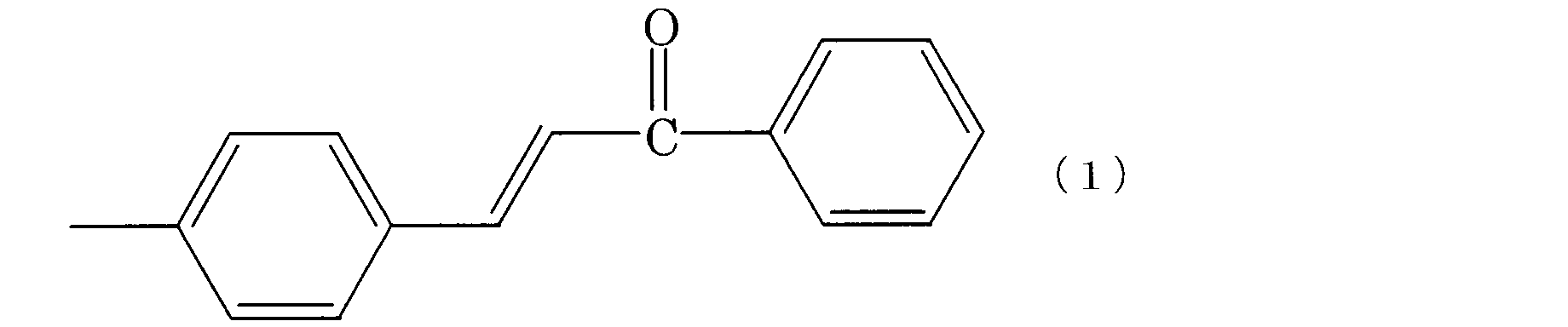




なお、本実施形態においては、配向膜材料として、光に反応し、光線の照射方向に液晶分子のプレチルト角を生じる光配向膜材料を使用したが、非特許文献1に開示の光配向法のように、光の照射領域の移動方向によってプレチルト方向の規定が可能である光配向膜材料を用いてもよい。この場合は、光を基板に対して斜めから入射させる必要はなく、基板に対して略垂直に入射させることができる。
次に、光配向膜の露光工程について説明する。まず、本実施形態の露光装置30について説明する。
図4、5に示すように、露光装置30は、1ステージタイプの走査型露光装置であり、複数の露光ヘッド31を含む露光ステージ32と、マザーガラス基板10を載置して所定方向に移動させるテーブル33とを備える。テーブル33は、移動手段としても機能する。なお、露光装置30は、露光ステージ32を移動させる移動手段を備えてもよいし、移動手段として機能せず、マザーガラス基板10を載置するテーブルと、露光ステージ32を移動させる移動手段とを備えてもよい。
複数の露光ヘッド31は、基板10の移動方向(走査方向)aに対して直交する方向bに、間隔をあけて配置されている。各露光ヘッド31は、基板10の被照射面に平行な面内を方向bに移動可能な状態で支持されている。
各露光ヘッド31は、紫外線を発する紫外線光源34と、フォトマスク50と、光源34及びフォトマスク50の間に設けられた偏光フィルタ、光学レンズ等の光学部材(図示せず)とを備え、フォトマスク50を介して基板10の表面に所定の照射角度(基板10の面の法線方向と、露光光の照射方向とのなす角度、例えば、40°)で偏光紫外線を照射できるように構成される。各光学部材は、光源34が発した紫外線を所望の露光光に光学的に変換する。光源34は、照射対象に応じて適宜選択すればよく、可視光線を発する光源であってもよい。
また、各露光ヘッド31は、撮像手段35と、記憶手段と、照合手段と、マスク移動手段とを備える。撮像手段35は、基板10の表面を撮影でき、基板10のパターン(例えば、ソースバスライン12、ゲートバスライン13、ブラックマトリックス16等)を読み取ることができる。撮像手段35には、例えばCCDカメラ等のカメラが適用できる。記憶手段は、露光の位置合わせの基準となる基準画像を記憶しておくことができる。照合手段は、撮像手段35が撮影した画像と基準画像とを比較照合して、実際に露光している位置と露光すべき位置とのズレを算出する。マスク移動手段は、照合手段によるズレの算出結果に基づいて、マスク50の位置や角度を補正する。これにより、基板10のパターンを読み取り、基板10の露光光に対する相対的な移動方向及び位置を高精度に制御しながら、走査露光を行うことができる。なお、照合手段は、基準画像を用いる代わりに、基板10を撮像した結果とマスク50を撮像した結果とを比較照合する方法によっても、同様にマスク50の位置及び角度を補正することができる。
マスク50は、その表面が基板10の被照射面に略平行となるように配置され、マスク50と、基板10の被照射面、すなわち光配向膜の表面との間にはプロキシミティギャップ41が設けられている。
マスク50は、例えば板状の部材であり、図6に示すように、石英ガラス等を用いて形成された透明基板と、透明基板の表面に所定のパターン(好適にはストライプ状のパターン)で形成された遮光部52及び複数の透光部51とを有する。各透光部51は、長手状であり、複数の透光部51は、所定のピッチで、基板10の移動方向aに対して直交する方向bに並んでいる。また、マスク50は、図7に示すように、中央領域53及びオーバーラップ領域54を有する。そして、オーバーラップ領域54内に設けられた透光部56(上記第2透光部に対応)の長さは、中央領域53から離れるにしたがって徐々に短くなっている。このようにして、オーバーラップ領域54内に設けられた透光部56の開口率が中央領域53内に設けられた透光部55(上記第1透光部に対応)の開口率よりも小さくなっている。換言すると、透光部55からより離れた透光部56ほど、その長さはより短く、また、その開口率はより小さい。
このようなマスク50の直下を基板10が通過すると、透光部51の直下を通過した領域のみが露光される。この結果、図8に示すように、基板10の表面の所定の細長い線状の領域18が露光される。なお、透光部51の材質は、光(例えば偏光紫外線)を透過することができれば特に限定されない。透光部51は、例えば、マスク50を貫通する開口部であってもよい。
走査露光方式を採用した本実施形態では、マスク50の透光部51の長さYと、基板10の移動速度(走査速度)Vで照射量が設定されている。より具体的には、光配向膜への照射量は次式で計算される。
(照射量)=(照度)×(透光部の長さY)/(基板の移動速度V)
なお、照度とは、より詳細には、露光光の光配向膜上での照度を意味する。したがって、照度及び移動速度Vを一定に保てば、照射量は、透光部の長さYに比例することとなる。
(照射量)=(照度)×(透光部の長さY)/(基板の移動速度V)
なお、照度とは、より詳細には、露光光の光配向膜上での照度を意味する。したがって、照度及び移動速度Vを一定に保てば、照射量は、透光部の長さYに比例することとなる。
図9は、光配向膜への照射量と、液晶分子のプレチルト角との関係を示すグラフである。図9に示すように、一般的に、光配向膜への照射量が大きくなるほど、該配向膜近傍の液晶分子のプレチルト角は、小さくなっていく。このように、プレチルト角は、照射量に依存し、プレチルト角を制御する上で照射量は非常に重要な要素である。また、特許文献4に記載されているように、VATNモードでは、プレチルト角を高精度に制御することが極めて重要である。
次に、露光装置30を用いてマザーガラス基板10を露光する方法について説明する。本実施形態では、マザーガラス基板10の露光すべき領域を複数の領域に分割して露光(光配向処理)する。まず、アレイ基板用のマザーガラス基板10aについて説明する。
図10に示すように、アレイ基板用フォトマスク60は、略長方形の板状の部材である。そして偏光紫外線が通過できるスリット状の透光部61が、所定のピッチPxで複数平行に形成されている。ピッチPxは、ソースバスライン12のピッチに等しく設定される。また、透光部61のピッチ方向の寸法Lxは、ソースバスライン12のピッチの約1/2の寸法に設定される。また、マスク60は、中央領域及びオーバーラップ領域を有し、オーバーラップ領域内に設けられた透光部の開口率が中央領域内に設けられた透光部の開口率よりも小さくなっている。
そして、図11、12に示すように、基板10a及びテーブルを+x軸方向に等速で移動させながら、フォトマスク60を介して、基板10aの表面に設けられた光配向膜19の端から端まで偏光紫外線を照射する(第1露光(1))。このとき、基板10aは、ソースバスライン12がフォトマスク60の透光部61の長手方向に沿うように移動させられる。この第1露光(1)の結果、フォトマスク60の中央領域が通過した領域21内と、フォトマスク60のオーバーラップ領域が通過した領域22内とにおいて、図2で示した絵素領域の領域A1が露光されることとなる。ただし、オーバーラップ領域内に設けられた透光部の開口率が中央領域内に設けられた透光部の開口率よりも小さいため、領域22内における領域A1の照射量は、領域21内における領域A1の照射量よりも小さくなる。また、フォトマスク60の透光部61が通過しなかった領域23内の絵素領域は、この段階では、露光されていない。
次に、基板10a及びテーブルを-x軸方向に移動させ、露光ステージ32の手前の位置に戻す。また、各露光ヘッド31を1つの露光ヘッド分だけ+y軸方向に移動させる。その結果、フォトマスク60の中央領域が領域23に対応して配置され、フォトマスク60のオーバーラップ領域が領域22に対応して配置される。
そして、図11、12に示すように、基板10a及びテーブルを+x軸方向に等速で移動させながら、フォトマスク60を介して、基板10aの表面に設けられた光配向膜19の端から端まで偏光紫外線を照射する(第1露光(2))。このとき、基板10aは、ソースバスライン12がフォトマスク60の透光部61の長手方向に沿うように移動させられる。この第1露光(2)の結果、フォトマスク60の中央領域が通過した領域23内において、絵素領域の領域A1が露光されることとなる。また、フォトマスク60のオーバーラップ領域が通過した領域22内において、領域A1が再び露光されることとなる。このように、第1露光(1)及び第1露光(2)は、同じ領域A1を照射する。ただし、領域22内における第1露光(1)による領域A1の照射量と、領域22内における第1露光(2)による領域A1の照射量との合計は、領域21内における第1露光(1)による領域A1の照射量よりも小さく、また、領域23内における第1露光(2)による領域A1の照射量よりも小さい。なお、光配向膜19の一部であって、領域21、領域22及び領域23内の領域A1にある部分は、それぞれ、上記第1部分、上記第2部分及び上記第3部分に対応する。
次に、基板10a及びテーブルを-x軸方向に移動させ、露光ステージ32の手前の位置に戻す。また、基板10aを面内で180°回転させてテーブル上に載置する。更に、各露光ヘッド31を1つの露光ヘッド分だけ-y軸方向に移動させる。その結果、フォトマスク60は、第1露光(1)時の位置とほぼ同じ位置に配置される。ただし、フォトマスク60は、第1露光(1)時の位置に比べて、ソースバスライン12のピッチの半分だけy軸方向にずれた位置に配置される。
そして、図11、12に示すように、基板10a及びテーブルを+x軸方向に等速で移動させながら、フォトマスク60を介して、基板10aの表面に設けられた光配向膜19の端から端まで偏光紫外線を照射する(第2露光(1))。このとき、基板10aは、ソースバスライン12がフォトマスク60の透光部61の長手方向に沿うように移動させられる。この第2露光(1)の結果、フォトマスク60の中央領域が通過した領域21内と、フォトマスク60のオーバーラップ領域が通過した領域22内とにおいて、図2で示した絵素領域の残りの領域A2が露光されることとなる。ただし、領域22内における領域A2の照射量は、領域21内における領域A2の照射量よりも小さくなる。また、フォトマスク60の透光部61が通過しなかった領域23内の絵素領域の領域A2は、この段階では、露光されていない。
次に、基板10a及びテーブルを-x軸方向に移動させ、露光ステージ32の手前の位置に戻す。また、各露光ヘッド31を1つの露光ヘッド分だけ+y軸方向に移動させる。その結果、フォトマスク60の中央領域が領域23に対応して配置され、フォトマスク60のオーバーラップ領域が領域22に対応して配置される。そして、フォトマスク60は、第1露光(2)時の位置とほぼ同じ位置に配置される。ただし、フォトマスク60は、第1露光(2)時の位置に比べて、ソースバスライン12のピッチの半分だけy軸方向にずれた位置に配置される。
そして、図11、12に示すように、基板10a及びテーブルを+x軸方向に等速で移動させながら、フォトマスク60を介して、基板10aの表面に設けられた光配向膜19の端から端まで偏光紫外線を照射する(第2露光(2))。このとき、基板10aは、ソースバスライン12がフォトマスク60の透光部61の長手方向に沿うように移動させられる。この第2露光(2)の結果、フォトマスク60の中央領域が通過した領域23内において、絵素領域の領域A2が露光されることとなる。また、フォトマスク60のオーバーラップ領域が通過した領域22内において、絵素領域の領域A2が再び露光されることとなる。このように、第2露光(1)及び第2露光(2)は、同じ領域A2を照射する。ただし、領域22内における第2露光(1)による領域A2の照射量と、領域22内における第2露光(2)による領域A2の照射量との合計は、領域21内における第2露光(1)による領域A2の照射量よりも小さく、また、領域23内における第2露光(2)による領域A2の照射量よりも小さい。なお、光配向膜19の一部であって、領域21、領域22及び領域23内の領域A2にある部分は、それぞれ、上記第1部分、上記第2部分及び上記第3部分に対応する。
以上の結果、基板10aは、全面にわたって露光され、基板10aの光配向処理が完了する。そして、図13に示すように、基板10aには、1度のみ露光された通常露光部24と、2回露光された露光継ぎ部25とが形成されることになる。なお、光配向膜19の一部であって、通常露光部24内にある部分は、上記第1及び第3部分に対応し、光配向膜19の一部であって、露光継ぎ部25内にある部分は、上記第2部分に対応する。
図14は、フォトマスク60に形成されるパターンと、露光工程におけるフォトマスク60の配置場所とを模式的に示した平面図である。フォトマスク60は、図14に示すように、中央領域63及びオーバーラップ領域64を有する。オーバーラップ領域64の幅は、10~80mm(好適には、30~60mm、例えば45mm)である。オーバーラップ領域64内に設けられた透光部66(上記第2透光部に対応)の長さyは、中央領域63内に設けられた透光部65(上記第1透光部に対応)の長さy0よりも小さくなっている。また、中央領域63から離れるにしたがって、透光部66の長さyは徐々に短くなっており、これにより、透光部66の開口率が徐々に減少している。したがって、第1露光(1)又は第2露光(1)において相対的に長い透光部66を通して露光された部分は、第1露光(2)又は第2露光(2)において相対的に短い透光部66を通して露光されることになる。透光部66の長さ(開口率)は、好適には、線形関数又は三角関数に従って変化している。また、露光継ぎ部25内において、第1露光(1)と第1露光(2)同士、第2露光(1)と第2露光(2)同士が同一部分(例えば絵素の同一の片側半分)を露光するように、マスク60は設計されている。
なお、中央領域63から離れるにしたがって、透光部66の開口率を徐々に減少させる方法は特に限定されず、例えば、特許文献3に記載の方法を適宜採用することができる。また、透光部66の長さを一定に保った状態で透光部66に網掛けをし、この網掛けの濃度を中央領域63から離れるにしたがって徐々に濃くする方法でもよい。
図15は、通常露光部24と露光継ぎ部25における照射量を示したグラフである。通常露光部24の照射量E0は、中央領域63内に設けられた透光部65の長さy0に比例し、位置xに関わらず一定である。露光継ぎ部25の照射量Eは、オーバーラップ領域64内に設けられた透光部66の長さyに比例するため、通常露光部24から離れるにしたがって徐々に減少している。露光継ぎ部25は、上述のように2回露光されるので、露光継ぎ部25の合計照射量は、第1露光(1)による照射量及び第1露光(2)による照射量の和、又は、第2露光(1)による照射量及び第2露光(2)による照射量の和となる。すなわち、露光継ぎ部25の合計照射量は、各露光による照射量に依存し、最大値Emaxを有する場合もあれば、最小値Eminを有する場合もある。しかしながら、本実施形態では、上述のように、露光継ぎ部25の合計照射量が通常露光部24の照射量E0よりも小さくなるように、フォトマスク60を設計している。これにより、隣接する通常露光部24の間で継ぎ目が発生するのを効果的に抑制することができる。
図16は、図11及び12で示した露光工程後の基板について、各絵素内における各種方向の関係を模式的に示した平面図である。図16に示すように、第1露光(1)、(2)と、第2露光(1)、(2)との間で、偏光紫外線の照射方向(光軸の方向でもよい。)の基板面への射影方向Aは、互いに、平行でかつ180°異なる向きとなる。また、第1露光(1)、(2)と、第2露光(1)、(2)との間で、基板の移動方向Bは、互いに、平行でかつ180°異なる向きとなる。その結果、第1露光(1)及び/又は第1露光(2)によって露光された領域A1と、第2露光(1)及び/又は第2露光(2)によって露光された領域A2との間で、光配向膜近傍の液晶分子のチルト方向Cは、互いに、平行でかつ180°異なる向きとなる。なお、チルト方向は、図17に示すように、光配向膜近傍の液晶分子4bの長軸の基板10の面への射影方向を意味する。また、チルト角θは、液晶分子4bの長軸と、基板10の面とのなす角を意味する。また、本実施形態において、上記射影方向Aと、基板の移動方向Bとの関係は、全ての露光(第1露光(1)、(2)及び第2露光(1)、(2))において同一である。
次に、カラーフィルタ基板用のマザーガラス基板10bに対する露光方法について説明する。
図18に示すように、カラーフィルタ基板用フォトマスク70は、アレイ基板用フォトマスク60とほぼ同一の構成を備える。すなわち、偏光紫外線が通過できるスリット状の透光部71が、所定のピッチPyをおいて複数平行に形成される。ピッチPyは、ブラックマトリックス16のピッチ(ここでは、アレイ基板と重ね合わせた場合に、アレイ基板のゲートバスライン13に平行する辺のピッチ)と等しくなるように設定される。また、透光部71のピッチ方向の寸法Lyは、ブラックマトリックス16のピッチの約1/2の寸法に設定される。また、マスク70は、中央領域及びオーバーラップ領域を有し、オーバーラップ領域内に設けられた透光部の開口率が中央領域内に設けられた透光部の開口率よりも小さくなっている。
そして、露光装置30を用いてマザーガラス基板10bを露光する。マザーガラス基板10bに対する露光態様は、基板の向きが90°異なるだけで、アレイ基板用のマザーガラス基板10aに対する露光態様とほぼ同様であるので、その詳細な説明は省略する。この結果、領域B1は、第1露光(1)及び/又は第1露光(2)によって露光され、領域B2は、第2露光(1)及び/又は第2露光(2)によって露光される。
その後、基板10a、10bを各パネル領域に分断し、アレイ基板1及びカラーフィルタ基板2を作製する。そして、配向処理が施された基板1、2の貼り合わせ工程を行う。貼り合わせ工程では、一方の基板の額縁領域にシール材を塗布する。次に、例えば粒径4μmのプラスチックビーズをシール材が塗布された基板上に散布した後、両基板を貼り合わせる。そして、図19に示すように、両基板1、2の間に、誘電率異方性が負のネマチック液晶材料を封入し、液晶層3を形成することによって、液晶表示パネルが完成する。
なお、液晶表示パネルの作製には、以下のようなプロセスを採用してもよい。まず、基板10a、10bの一方について、各パネル領域11の額縁領域にシール材を塗布する。次に、他方の基板表面に、誘電率異方性が負のネマチック液晶材料を所定のピッチで点状に滴下する。そして、このように処理した両基板を真空環境下で貼り合わせる。セル厚は、カラーフィルタ基板用のマザーガラス基板10bに予め設置されたフォトスペーサーによって制御され、例えば4μmに設定される。その後、シール材を硬化し、各パネルに分断して液晶表示パネルが完成する。
液晶層3内の液晶分子4は、駆動電圧が液晶層3に印加されていないとき(電圧無印加時)には、光配向膜19の表面に対して略垂直方向に配向される。実際には、液晶分子4は、このとき、光配向膜19の表面の法線方向に対して0.1°程度から数°程度、若干傾いて配向される。すなわち、液晶分子4は、若干のプレチルト角を有するように、光配向19により配向されている。なお、プレチルト角とは、電圧無印加時におけるチルト角を意味する。
図20は、各絵素内における液晶分子の配向方向を模式的に示した図である。上記のように配向処理が施されたアレイ基板及びカラーフィルタ基板を貼り合わせて液晶表示パネルを構成すると、液晶分子は、各基板の各領域に施された配向処理の向き、すなわち偏光紫外線の照射方向にしたがって配向する。その結果、図20に示すように、アレイ基板近傍の液晶分子のチルト方向(図20中の点線矢印)と、カラーフィルタ基板近傍の液晶分子のチルト方向(図20中の実線矢印)とは、互いに略直交する。そして、各絵素内には、液晶分子の配向の向きが互いに異なる4つのドメインD1~D4が形成される。各ドメインにおいて、液晶分子は、略90°捩れて配向する。また、各ドメインにおいて、液晶分子は、液晶層3に閾値以上の充分な駆動電圧が印加されたとき(電圧印加時)、両基板のチルト方向を2等分する方位に倒れる。例えば、両基板表面から等距離に位置する液晶分子4aは、電圧印加時、45°方位、135°方位、225°方位、又は、315°方位に倒れる。また、液晶分子4aは、両基板の面に対して略平行な方向にまで傾斜する。
次に、図19に示すように、基板1、2の外側に、2枚の位相差板7a、7b、及び、2枚の偏光板6a、6bを貼り付ける。なお、位相差板7a、7bは、設置しなくともよいが、広視野角を実現する観点からは、設置することが好ましい。また、位相差板7a、7bは、どちらか一方のみが配置されてもよい。偏光板6a、6bは、クロスニコルに配置されている。また、偏光板6a、6bの一方は、その吸収軸がアレイ基板近傍の液晶分子のチルト方向(図20中の点線矢印)と平行となるように配置され、他方は、その吸収軸がカラーフィルタ基板近傍の液晶分子のチルト方向(図20中の実線矢印)と平行となるように配置される。上述のように、電圧無印加時に、液晶分子は、ほぼ垂直配向するため、本実施形態の液晶表示パネルは、良好な黒表示(ノーマリーブラックモード)を実現することができる。また、本実施形態の液晶表示パネルは、4つのドメインを有し、4つのドメインの液晶分子は、互いに異なる4方向に応答するため、視角方向にほとんど依存しない表示特性を示すことができる。
図21は、実施形態1に係る液晶表示パネルにおいて、1つの絵素における明るさをシミュレーションした結果を示す。図21に示すように、実施形態1に係る液晶表示パネルにおいては、4つのドメインD1~D4内における液晶分子4aの倒れる方向は、互いに略90°の角度をなしている。したがって、異なるドメインの境界においては、液晶分子4aは、互いに異なる方向に倒れた液晶分子4aを連続的に繋ぐように配向することになる。また、4つのドメインD1~D4内における液晶分子4aの倒れる方向は、偏光板6a、6bの吸収軸方向に対して略45°異なる。その結果、異なるドメインの境界における液晶分子4aの配向方位は、偏光板6aの吸収軸方向、又は、偏光板6bの吸収軸方向と略同一又は略直交する方位となる。したがって、異なるドメインの境界において、下側の偏光板6aを透過した偏光には、液晶分子によるリターデーション(位相差)が発生しない。すなわち、下側の偏光板6aを透過した偏光は、液晶層3で何ら影響を受けず、下側の偏光板6aを透過した偏光は、上側の偏光板6bを透過することができない。その結果、異なるドメインの境界において輝度の低い、暗い線、すなわち暗線が発生することとなる。
なお、図20、21では、カラーフィルタ基板側からパネルを観察したときに、逆卍状の暗線が発生するように液晶分子の配向方向が設定された場合を示しているが、液晶分子の配向方向は、図37~39に示すように設定されてもよい。図37~39において、点線矢印は、アレイ基板近傍の液晶分子のチルト方向を示し、実線矢印は、カラーフィルタ基板近傍の液晶分子のチルト方向を示す。カラーフィルタ基板側からパネルを観察したときに、図37に示す場合は卍状の暗線が発生し、図38に示す場合は8の字状の暗線が発生し、図39に示す場合は逆8の字状の暗線が発生する。また、図26等に示すように、1つの絵素領域を2つの領域に分割し、各領域内に4つのドメインを形成してもよい。
その後、一般的なモジュール製造工程を経て、実施形態1の液晶表示装置を完成することができる。
本実施形態の液晶表示装置は、4ドメインのVATNモードである。4ドメインのVATNモードによれば、基板10a、10bをそれぞれ2回照射し、合計4回の照射で4つのドメインを形成することができる。そのため、装置台数の削減と配向処理時間の短縮(タクトタイムの短縮)とが実現できる。また、1絵素を4ドメインに分割させることは液晶表示装置の広視野角化を実現する観点から好ましい形態である。更に、従来のMVAモード等のように配向制御構造物を有する液晶モードにおいて必要であったリブ(突起)等の配向制御構造物を形成するためのフォトマスク、すなわちフォトリソ工程を削減することができ、その結果、製造プロセスの簡略化が可能となる。なお、1画素(1サブ画素)を2ドメインに分割させた場合には、例えば上下又は左右のどちらかの方向については広視野角化できるが、他方の方向の視野角特性を向上することはできない。また、5つ以上にドメインを増やしても構わないが、プロセスが煩雑となる上、処理時間も長くなるためあまり好ましくない。更に、4ドメインとそれ以上のドメインとでは、視野角特性には実用上それ程違いがないことも分かっている。
本実施形態で使用可能な材料及び適応可能な製造プロセスにおける条件としては下記が挙げられる。ただし、本実施形態で使用可能な材料及び条件は、下記に限定されるものではない。また、露光に用いる光線の種類は偏光紫外線に特に限定されず、配向膜材料、製造プロセス等によって適宜設定することができ、無偏光(消光比=1:1)であってもよい。
・液晶材料:Δn(複屈折)=0.06~0.14、Δε(誘電率異方性)=-2.0~-8.0、Tni(ネマチック-アイソトロピック相転移温度)=60~110℃を有するネマチック液晶。
・プレチルト角:85~89.9°
・セル厚:2~5μm
・照射エネルギー密度:0.01~5J/cm2
・プロキシミティギャップ:100~300μm
・光源:低圧水銀ランプ、高圧水銀ランプ、重水素ランプ、メタルハライドランプ、アルゴン共鳴ランプ、キセノンランプ、エキシマーレーザ
・紫外線の消光比(偏光度):1:1~60:1
・紫外線の照射方向:基板面法線方向から0~70°(例えば40°)方向
・液晶材料:Δn(複屈折)=0.06~0.14、Δε(誘電率異方性)=-2.0~-8.0、Tni(ネマチック-アイソトロピック相転移温度)=60~110℃を有するネマチック液晶。
・プレチルト角:85~89.9°
・セル厚:2~5μm
・照射エネルギー密度:0.01~5J/cm2
・プロキシミティギャップ:100~300μm
・光源:低圧水銀ランプ、高圧水銀ランプ、重水素ランプ、メタルハライドランプ、アルゴン共鳴ランプ、キセノンランプ、エキシマーレーザ
・紫外線の消光比(偏光度):1:1~60:1
・紫外線の照射方向:基板面法線方向から0~70°(例えば40°)方向
以上説明したように、本実施形態では、露光継ぎ部の合計照射量が通常露光部の照射量E0よりも小さくなるように露光処理が施されている。これにより、隣接する通常露光部の間で継ぎ目が発生するのを効果的に抑制することができる。
常識的には、或いは、直感的には、通常露光部の照射量E0を100%とした場合、露光継ぎ部の合計照射量は100%にするようにすべきと思われる。すなわち、図14及び図15で露光継ぎ部の合計照射量が位置xに関わらず一定で100%とする場合である。そこで本発明者らは次のようなパネルを試作した。
試作ではカラーフィルタ基板で露光継ぎ部の合計照射量の調整を行った。簡単のため、アレイ基板では継ぎ露光を行わない一括露光を行った。すなわち、アレイ基板の全面を一括して露光した。また、アレイ基板における第1露光及び第2露光の方位は、左右方向とした。
図22に示すように、試作では、フォトマスク70を含む複数の露光ヘッドを備える露光装置を使用した。試作パネルでは、4つの通常露光部24の間に、合計3つの露光継ぎ部25が発生した。また、図23に示すように、各フォトマスク70には、中央領域73及びオーバーラップ領域74を設け、中央領域73内に互いの長さが同じ透光部75(上記第1透光部に対応)を設け、オーバーラップ領域74内に透光部76(上記第2透光部に対応)を設け、透光部76の長さは、中央領域73から離れるにしたがって徐々に短くなるように設定した。また、露光継ぎ部において、第1露光(1)と第1露光(2)同士、第2露光(1)と第2露光(2)同士が同一部分(例えば絵素の同一の片側半分)を露光するように、マスク70を設計した。
そして、パネル試作には、マスク70として、以下の3種類のマスクを使用し、パネル1~3を作製した。第1のマスクは、露光継ぎ部の合計照射量が一定で100%となるように設計した。第2、第3のマスクは、露光継ぎ部の合計照射量が100%より高くなるように設計されており、第2のマスクは、露光継ぎ部の最大照射量Emaxが125%となるよう、第3のマスクは、露光継ぎ部のEmaxが150%となるように設計した。
試作パネル1~3において、露光継ぎ部の見え方を目視によって評価した結果を説明する。図24に示すように、正面方向、左右方向(0°又は180°方位)、上下方向(90°又は270°方位)から試作パネル1~3を観察した。得られた結果(1)~(4)を以下に示す。
(1)正面方向から見ると、全階調に渡って露光継ぎ部25は目視できなかった。
(2)左右方向(0°又は180°方位)において斜めから見ると、グレー階調(低階調)で、露光継ぎ部25が短冊状に通常露光部24と比べて明るく見えた。
(3)上下方向(90°又は270°方位)において斜めから見ると、低階調で露光継ぎ部25が短冊状に通常露光部24と比べて暗く見えた。
(4)150%、125%、100%の順に上記見え方の程度は軽くなってはいくが、100%の場合でも露光継ぎ部25が目視で視認された。
(2)左右方向(0°又は180°方位)において斜めから見ると、グレー階調(低階調)で、露光継ぎ部25が短冊状に通常露光部24と比べて明るく見えた。
(3)上下方向(90°又は270°方位)において斜めから見ると、低階調で露光継ぎ部25が短冊状に通常露光部24と比べて暗く見えた。
(4)150%、125%、100%の順に上記見え方の程度は軽くなってはいくが、100%の場合でも露光継ぎ部25が目視で視認された。
図25に、左右方向(0°又は180°方位)において斜め60°方向からの輝度ムラを測定した結果を示す。これは、横方向に輝度計をスキャンしながら測定した。図25に示すように、輝度計の測定でも上記の目視結果(4)の傾向が再現された。すなわち、100%では露光継ぎ部に対する露光が依然過剰になっていると言える。
図26は、試作パネル1~3について、通常露光部にある各絵素内における液晶分子の配向方向を模式的に示した図である。図27は、試作パネル1~3について、露光継ぎ部にある各絵素内における液晶分子の配向方向を模式的に示した図である。図26、27において、実線矢印は、カラーフィルタ基板上のチルト方向を、点線矢印は、アレイ基板上のチルト方向を示す。通常露光部では、アレイ基板上のチルト角と、カラーフィルタ基板上のチルト角とがほぼ等しく、図26に示すように、液晶分子は、両基板のチルト方向を2等分する方位に倒れる。それに対して、露光継ぎ部では電圧印加時に液晶分子がカラーフィルタ基板上のチルト方向に引っ張られて倒れると推察される。つまり、露光継ぎ部では合計照射量が100%であっても通常露光部よりチルト角が低いと考えられる。そのため、図27に示すように、左右方向からは液晶分子の腹の部分(位相差の大きい部分)をより見ることになり、通常露光部に比べて明るく見え、上下方向からは液晶分子の頭の部分(位相差の小さい部分)をより見ることになり、通常露光部に比べて暗く見えると考えられる。
この試作の結果より、特に走査露光方式においては、通常露光部の照射量に対する露光継ぎ部の合計照射量の割合(百分率)を100%未満にする必要があることが今回初めて明らかとなった。
露光継ぎ部の最適な合計照射量を見出すべく、合計照射量を100%未満で細かく振ったパネル4~13(Emin=74.8~95.8%)を試作した。ここではアレイ基板側で継ぎ露光を実施した。先の試作とは異なり、ここではアレイ基板を6個の領域に分割し、縦方向に走査露光した。すなわち、本試作では、図28に示すように、露光継ぎ部25は、5つ存在する。なお、露光継ぎ部25の幅は、45mmに設定した。
各パネルについて、図29に示すように、露光継ぎ部25を左右方向で斜め方向から、NDフィルタを介さず、又は、NDフィルタを介して、目視で観察した。その結果を下記表1に示す。観察は、露光継ぎ部が最も見えやすい階調である32階調で行った。NDフィルタ越しの評価においては、NDフィルタ越しに継ぎ目が目視できない場合はOKとし、目視できる場合はNGとした。すなわち、例えば、ND1%OKとは、1%NDフィルタ越しに露光継ぎ部が見えないことを意味し、ND3%NGとは、3%NDフィルタ越しに露光継ぎ部が見えることを意味する。なお、ND値が小さくなるほど、フィルタからの透過光量は低下する。

図30は、試作パネル4~13について、通常露光部にある各絵素内における液晶分子の配向方向を模式的に示した図である。図31は、試作パネル4~13について、露光継ぎ部にある各絵素内における液晶分子の配向方向を模式的に示した図である。図30、31において、実線矢印は、カラーフィルタ基板上のチルト方向を、点線矢印は、アレイ基板上のチルト方向を示す。いずれのパネルについても、通常露光部では、アレイ基板上のチルト角と、カラーフィルタ基板上のチルト角とがほぼ等しく、図30に示すように、液晶分子は、両基板のチルト方向を2等分する方位に倒れる。例えば露光継ぎ部の最小照射量が74.8%の場合は左右方向で斜め方向から露光継ぎ部が暗く見えた。この原因としては74.8%では露光継ぎ部の照射量が不足しており、アレイ基板上において、露光継ぎ部のチルト角が通常露光部のチルト角よりも高くなって、電圧印加時に液晶分子がカラーフィルタ基板側のチルト方向に引っ張られて倒れているためと考えられる。その結果、図31に示すように、左右方向で斜めから見た際には液晶分子の頭の部分(位相差のより小さい部分)をより見ることになり、露光継ぎ部以外より暗く見えると考えられる。
85.2<Emin<100の範囲であれば、露光継ぎ部は若干、暗く見えるが、ND3%OKレベルであり、実使用上は許容できる範囲内である。また、91.5≦Emin≦95.8の範囲であれば、ND10%OKレベルであり、全く問題ない良品パネルであると言える。今回の結果から、本実施形態において、露光継ぎ部の合計照射量の範囲は、好ましくは、85<Emin<100であり、より好ましくは、91≦Emin≦96であると言える。
なお、本実施形態では、1つのステージ32を有する露光装置30について説明したが、露光装置30は複数のステージを有してもよい。例えば、第1露光(1)、第1露光(2)、第2露光(1)、第2露光(2)それぞれに対してステージを設けてもよい。
(実施形態2)
本実施形態は、使用する露光装置が異なり、露光工程の態様が異なる点を除いて、実施形態1とほとんど同じである。
本実施形態は、使用する露光装置が異なり、露光工程の態様が異なる点を除いて、実施形態1とほとんど同じである。
本実施形態に係る露光装置は、図32に示すように、複数の露光ヘッド231を含む露光ステージ232を備える。各露光ヘッド231は、第1露光(1)、(2)用の光源及び光学部材と、第2露光(1)、(2)用の光源及び光学部材と、フォトマスク250とを有する。各フォトマスク250には、第1露光(1)、(2)用の透光部パターン251aと、第2露光(1)、(2)用の透光部パターン251bとが形成されている。図33に示すように、透光部パターン251a、251bは、例えば、互いに絵素ピッチの半分だけずれて配置されている。マスク250は、中央領域253及びオーバーラップ領域254を有する。オーバーラップ領域254内に設けられた透光部の長さは、中央領域253から離れるにしたがって徐々に短くなっている。
そして、図32、34に示すように、第1露光(1)、(2)用の光源から生成された偏光紫外線を透光部パターン251aに照射し、第2露光(1)、(2)用の光源から生成された偏光紫外線を透光部パターン251bに照射した状態で、基板10をマスク250の下を通過させる。これらの偏光紫外線は、互いに反対方向から照射されている。これにより、第1露光(1)及び第2露光(1)を同時に実施でき、また、第1露光(2)及び第2露光(2)を同時に実施できる。すなわち、合計2回の走査露光を行うのみで基板10の配向処理が完了する。
なお、本実施形態では、図35に示すように、第1露光(1)、(2)と、第2露光(1)、(2)との間で、偏光紫外線の照射方向の基板面への射影方向Aと、基板の移動方向Bとの関係が互いに異なるが、光配向膜近傍の液晶分子のチルト方向Cは、実施形態1の場合と同じである。
また、本実施形態に係る露光装置は、複数のステージを有してもよい。例えば、第1露光(1)及び第2露光(1)用のステージと、第1露光(2)及び第2露光(2)用のステージとを設けてもよい。
(実施形態3)
本実施形態は、使用する露光装置が異なり、露光工程の態様が異なる点を除いて、実施形態1、2とほとんど同じである。
本実施形態は、使用する露光装置が異なり、露光工程の態様が異なる点を除いて、実施形態1、2とほとんど同じである。
本実施形態に係る露光装置において、各露光ヘッドは、図36に示すように、フォトマスク350及び遮光部材356を有する。フォトマスク350には、同じ長さの複数の透光部351が形成されているが、透光部351の開口率が徐々に減少するように端側の透光部351の一部が遮光部材356によって遮光されている。
本実施形態によっても、実施形態1、2と同様に、露光継ぎ部の合計照射量を通常露光部の照射量よりも小さくすることができる。
遮光部材356としては、光源からの光を部分的に遮断する部材であればよく、例えば、光シャッター、光ブラインド等を適宜選択できる。また、遮光部材356の配置位置をメカニカルに可変とする機構を部材356に設けてもよく、この場合は露光継ぎ部の照射量を容易に調整できるというメリットがある。
本願は、2011年1月24日に出願された日本国特許出願2011-012391号を基礎として、パリ条約ないし移行する国における法規に基づく優先権を主張するものである。該出願の内容は、その全体が本願中に参照として組み込まれている。
1:アレイ基板
2:カラーフィルタ基板
3:液晶層
4、4a、4b:液晶分子
6a、6b:偏光板
7a、7b:位相差板
10:マザーガラス基板
10a:アレイ基板用のマザーガラス基板
10b:カラーフィルタ基板用のマザーガラス基板
11:パネル領域
12:ソースバスライン
13:ゲートバスライン
14:薄膜トランジスタ
15:絵素電極
16:ブラックマトリックス
17:カラーフィルタ
19:光配向膜
18、21、22、23、A1、A2、B1、B2:領域
24:通常露光部
25:露光継ぎ部
30:露光装置
31、231:露光ヘッド
32、232:露光ステージ
33:テーブル
34:紫外線光源
35:撮像手段
41:プロキシミティギャップ
50、250、350:フォトマスク
52:遮光部
51、55、56、61、65、66、71、75、76、351:透光部
53、63、73、253:中央領域
54、64、74、254:オーバーラップ領域
60:アレイ基板用フォトマスク
70:カラーフィルタ基板用フォトマスク
251a、251b:透光部パターン
356:遮光部材
A:偏光紫外線の照射方向の基板面への射影方向
B:基板の移動方向
C:チルト方向
D1、D2、D3、D4:ドメイン
2:カラーフィルタ基板
3:液晶層
4、4a、4b:液晶分子
6a、6b:偏光板
7a、7b:位相差板
10:マザーガラス基板
10a:アレイ基板用のマザーガラス基板
10b:カラーフィルタ基板用のマザーガラス基板
11:パネル領域
12:ソースバスライン
13:ゲートバスライン
14:薄膜トランジスタ
15:絵素電極
16:ブラックマトリックス
17:カラーフィルタ
19:光配向膜
18、21、22、23、A1、A2、B1、B2:領域
24:通常露光部
25:露光継ぎ部
30:露光装置
31、231:露光ヘッド
32、232:露光ステージ
33:テーブル
34:紫外線光源
35:撮像手段
41:プロキシミティギャップ
50、250、350:フォトマスク
52:遮光部
51、55、56、61、65、66、71、75、76、351:透光部
53、63、73、253:中央領域
54、64、74、254:オーバーラップ領域
60:アレイ基板用フォトマスク
70:カラーフィルタ基板用フォトマスク
251a、251b:透光部パターン
356:遮光部材
A:偏光紫外線の照射方向の基板面への射影方向
B:基板の移動方向
C:チルト方向
D1、D2、D3、D4:ドメイン
Claims (24)
- 光配向膜が表面に設けられた基板を露光光に対して相対的に移動させながら前記光配向膜を露光する露光装置であって、
前記露光装置は、前記光配向膜の第1部分及び第2部分を露光する第1露光と、前記光配向膜の第3部分を露光するとともに前記第2部分を再び露光する第2露光とを行うものであり、
前記第2部分は、前記第1部分及び前記第3部分の間にあり、
前記第2部分の照射量が前記第1部分の照射量よりも小さくなるように、前記第1露光は行われ、
前記第2部分の照射量が前記第3部分の照射量よりも小さくなるように、前記第2露光は行われ、
前記第1露光による前記第2部分の前記照射量、及び、前記第2露光による前記第2部分の前記照射量の合計は、前記第1部分の前記照射量、及び、前記第3部分の前記照射量のいずれよりも小さく設定されることを特徴とする露光装置。 - 前記第1部分の前記照射量、及び/又は、前記第3部分の前記照射量を100%としたとき、
前記第2部分の前記照射量の合計の最小値は、85.2%より大きく、100%より小さいことを特徴とする請求項1記載の露光装置。 - 前記第2部分の前記照射量の合計の最小値は、91%以上、96%以下であることを特徴とする請求項2記載の露光装置。
- 前記露光装置は、紫外線を前記基板の面の法線に対して斜め方向から入射させるものであることを特徴とする請求項1~3のいずれかに記載の露光装置。
- 前記紫外線は、偏光紫外線であることを特徴とする請求項4記載の露光装置。
- 前記露光装置は、遮光部及び複数の透光部を含むフォトマスクを備え、
前記フォトマスクを介して前記光配向膜を露光することを特徴とする請求項1~4のいずれかに記載の露光装置。 - 前記遮光部及び前記複数の透光部は、ストライプ状に配置されることを特徴とする請求項6記載の露光装置。
- 前記複数の透光部の長手方向の方位と、前記基板の相対的な移動方向の方位とが実質的に同じであることを特徴とする請求項7記載の露光装置。
- 前記フォトマスクは、前記第1部分、及び/又は、前記第3部分に対応して設けられた複数の第1透光部と、前記第2部分に対応して設けられた複数の第2透光部とを含み、
各第2透光部の開口率は、各第1透光部の開口率よりも小さいことを特徴とする請求項6~8のいずれかに記載の露光装置。 - 前記複数の第2透光部の開口率は、前記複数の第1透光部から離れるにしたがって減少することを特徴とする請求項9記載の露光装置。
- 前記複数の第2透光部の開口率の変化は、線形関数又は三角関数で表されることを特徴とする請求項10記載の露光装置。
- 前記複数の第2透光部の長さは、前記複数の第1透光部から離れるにしたがって短くなることを特徴とする請求項10又は11記載の露光装置。
- 前記フォトマスク及び前記基板の間に、プロキシミティギャップが設けられることを特徴とする請求項6~12のいずれかに記載の露光装置。
- 前記基板のパターンを読み取る撮像手段を備えることを特徴とする請求項1~13のいずれかに記載の露光装置。
- 前記基板のパターンを読み取りながら前記基板の露光光に対する相対的な移動方向を制御することを特徴とする請求項14記載の露光装置。
- 請求項1~15のいずれかに記載の露光装置を用いて作製されたことを特徴とする液晶表示装置。
- VATNモードで駆動されることを特徴とする請求項16記載の液晶表示装置。
- 2以上のドメインを有することを特徴とする請求項16又は17記載の液晶表示装置。
- 光配向膜が表面に設けられた基板を露光光に対して相対的に移動させながら前記光配向膜を露光する露光工程を含む液晶表示装置の製造方法であって、
前記露光工程において、前記光配向膜の第1部分及び第2部分を露光する第1露光と、前記光配向膜の第3部分を露光するとともに前記第2部分を再び露光する第2露光とを行い、
前記第2部分の照射量が前記第1部分の照射量よりも小さくなるように、前記第1露光は行われ、
前記第2部分の照射量が前記第3部分の照射量よりも小さくなるように、前記第2露光は行われ、
前記第1露光による前記第2部分の前記照射量、及び、前記第2露光による前記第2部分の前記照射量の合計は、前記第1部分の前記照射量、及び、前記第3部分の前記照射量のいずれよりも小さく設定されることを特徴とする液晶表示装置の製造方法。 - 垂直配向型の液晶層を形成する工程を含むことを特徴とする請求項19記載の液晶表示装置の製造方法。
- 誘電率異方性が負の液晶材料を含有する液晶層を形成する工程を含むことを特徴とする請求項19又は20記載の液晶表示装置の製造方法。
- 前記露光工程によって露光処理された2枚の基板を、露光光の照射方向の当該基板の面への射影方向が互いに略直交するように、貼り合わせる工程を含むことを特徴とする19~21のいずれかに記載の液晶表示装置の製造方法。
- 前記基板を平面視したときに、互いに反平行方向に露光される2つの領域を各画素内に形成するように、前記光配向膜を露光する工程を含むことを特徴とする請求項19~22のいずれかに記載の液晶表示装置の製造方法。
- 請求項19~23のいずれかに記載の液晶表示装置の製造方法を用いて作製されたことを特徴とする液晶表示装置。
Applications Claiming Priority (2)
| Application Number | Priority Date | Filing Date | Title |
|---|---|---|---|
| JP2011012391 | 2011-01-24 | ||
| JP2011-012391 | 2011-01-24 |
Publications (1)
| Publication Number | Publication Date |
|---|---|
| WO2012102104A1 true WO2012102104A1 (ja) | 2012-08-02 |
Family
ID=46580676
Family Applications (1)
| Application Number | Title | Priority Date | Filing Date |
|---|---|---|---|
| PCT/JP2012/050662 Ceased WO2012102104A1 (ja) | 2011-01-24 | 2012-01-16 | 露光装置、液晶表示装置及びその製造方法 |
Country Status (2)
| Country | Link |
|---|---|
| TW (1) | TW201235799A (ja) |
| WO (1) | WO2012102104A1 (ja) |
Cited By (7)
| Publication number | Priority date | Publication date | Assignee | Title |
|---|---|---|---|---|
| WO2014034471A1 (ja) * | 2012-08-27 | 2014-03-06 | シャープ株式会社 | 液晶表示装置 |
| JP2016529489A (ja) * | 2013-07-12 | 2016-09-23 | ジェネンテック, インコーポレイテッド | イオン交換クロマトグラフィーのインプットの最適化の解明 |
| CN111290175A (zh) * | 2020-02-16 | 2020-06-16 | 南京中电熊猫液晶显示科技有限公司 | 一种掩膜版 |
| CN111566549A (zh) * | 2018-01-19 | 2020-08-21 | 堺显示器制品株式会社 | 液晶显示装置的制造方法及光掩模 |
| CN111856822A (zh) * | 2020-06-29 | 2020-10-30 | 南京中电熊猫平板显示科技有限公司 | 双层掩膜版及其使用方法、改善双层掩膜版的漏光方法 |
| CN112068396A (zh) * | 2020-09-25 | 2020-12-11 | 南京中电熊猫液晶显示科技有限公司 | 一种掩膜版 |
| WO2026079136A1 (ja) * | 2024-10-11 | 2026-04-16 | ソニーセミコンダクタソリューションズ株式会社 | 表示装置、電子機器、及び、表示装置の製造方法 |
Citations (2)
| Publication number | Priority date | Publication date | Assignee | Title |
|---|---|---|---|---|
| WO2007086474A1 (ja) * | 2006-01-26 | 2007-08-02 | Sharp Kabushiki Kaisha | 液晶表示装置の製造方法及び液晶表示装置 |
| WO2008069181A1 (ja) * | 2006-12-05 | 2008-06-12 | Sharp Kabushiki Kaisha | 液晶表示装置 |
-
2012
- 2012-01-16 TW TW101101633A patent/TW201235799A/zh unknown
- 2012-01-16 WO PCT/JP2012/050662 patent/WO2012102104A1/ja not_active Ceased
Patent Citations (2)
| Publication number | Priority date | Publication date | Assignee | Title |
|---|---|---|---|---|
| WO2007086474A1 (ja) * | 2006-01-26 | 2007-08-02 | Sharp Kabushiki Kaisha | 液晶表示装置の製造方法及び液晶表示装置 |
| WO2008069181A1 (ja) * | 2006-12-05 | 2008-06-12 | Sharp Kabushiki Kaisha | 液晶表示装置 |
Cited By (10)
| Publication number | Priority date | Publication date | Assignee | Title |
|---|---|---|---|---|
| WO2014034471A1 (ja) * | 2012-08-27 | 2014-03-06 | シャープ株式会社 | 液晶表示装置 |
| JP2016529489A (ja) * | 2013-07-12 | 2016-09-23 | ジェネンテック, インコーポレイテッド | イオン交換クロマトグラフィーのインプットの最適化の解明 |
| US10274466B2 (en) | 2013-07-12 | 2019-04-30 | Genentech, Inc. | Elucidation of ion exchange chromatography input optimization |
| US10921297B2 (en) | 2013-07-12 | 2021-02-16 | Genentech, Inc. | Elucidation of ion exchange chromatography input optimization |
| CN111566549A (zh) * | 2018-01-19 | 2020-08-21 | 堺显示器制品株式会社 | 液晶显示装置的制造方法及光掩模 |
| CN111566549B (zh) * | 2018-01-19 | 2023-03-24 | 堺显示器制品株式会社 | 液晶显示装置的制造方法及光掩模 |
| CN111290175A (zh) * | 2020-02-16 | 2020-06-16 | 南京中电熊猫液晶显示科技有限公司 | 一种掩膜版 |
| CN111856822A (zh) * | 2020-06-29 | 2020-10-30 | 南京中电熊猫平板显示科技有限公司 | 双层掩膜版及其使用方法、改善双层掩膜版的漏光方法 |
| CN112068396A (zh) * | 2020-09-25 | 2020-12-11 | 南京中电熊猫液晶显示科技有限公司 | 一种掩膜版 |
| WO2026079136A1 (ja) * | 2024-10-11 | 2026-04-16 | ソニーセミコンダクタソリューションズ株式会社 | 表示装置、電子機器、及び、表示装置の製造方法 |
Also Published As
| Publication number | Publication date |
|---|---|
| TW201235799A (en) | 2012-09-01 |
Similar Documents
| Publication | Publication Date | Title |
|---|---|---|
| JP5400176B2 (ja) | 露光装置及び液晶表示装置の製造方法 | |
| JP4606510B2 (ja) | 液晶表示装置の製造方法及び液晶表示装置 | |
| JP4666417B2 (ja) | 液晶表示装置の製造方法及び配向処理用露光装置 | |
| CN101622572B (zh) | 液晶显示装置及其制造方法 | |
| JP5079796B2 (ja) | 液晶表示装置の製造方法及び液晶表示装置 | |
| CN101765806B (zh) | 液晶显示装置及其制造方法 | |
| WO2012102104A1 (ja) | 露光装置、液晶表示装置及びその製造方法 | |
| US20120064441A1 (en) | Method for photo-alignment treatment, mask for photo-alignment treatment, and method for producing alignment film | |
| WO2012105393A1 (ja) | 露光装置、液晶表示装置及びその製造方法 | |
| Tang et al. | 39.1: Invited Paper: Novel Photo‐Alignment Material for Ultra‐High Definition VA LCDs |
Legal Events
| Date | Code | Title | Description |
|---|---|---|---|
| 121 | Ep: the epo has been informed by wipo that ep was designated in this application |
Ref document number: 12738969 Country of ref document: EP Kind code of ref document: A1 |
|
| NENP | Non-entry into the national phase |
Ref country code: DE |
|
| 122 | Ep: pct application non-entry in european phase |
Ref document number: 12738969 Country of ref document: EP Kind code of ref document: A1 |
|
| NENP | Non-entry into the national phase |
Ref country code: JP |