WO2012090936A1 - シンチレータ用発光材料、それを用いたシンチレータ及びそれを用いた放射線検出器並びに放射線検査装置 - Google Patents
シンチレータ用発光材料、それを用いたシンチレータ及びそれを用いた放射線検出器並びに放射線検査装置 Download PDFInfo
- Publication number
- WO2012090936A1 WO2012090936A1 PCT/JP2011/080076 JP2011080076W WO2012090936A1 WO 2012090936 A1 WO2012090936 A1 WO 2012090936A1 JP 2011080076 W JP2011080076 W JP 2011080076W WO 2012090936 A1 WO2012090936 A1 WO 2012090936A1
- Authority
- WO
- WIPO (PCT)
- Prior art keywords
- scintillator
- light
- raw material
- radiation
- radiation detector
- Prior art date
- Legal status (The legal status is an assumption and is not a legal conclusion. Google has not performed a legal analysis and makes no representation as to the accuracy of the status listed.)
- Ceased
Links
Images




Classifications
-
- G—PHYSICS
- G01—MEASURING; TESTING
- G01T—MEASUREMENT OF NUCLEAR OR X-RADIATION
- G01T1/00—Measuring X-radiation, gamma radiation, corpuscular radiation, or cosmic radiation
- G01T1/16—Measuring radiation intensity
- G01T1/20—Measuring radiation intensity with scintillation detectors
- G01T1/202—Measuring radiation intensity with scintillation detectors the detector being a crystal
-
- C—CHEMISTRY; METALLURGY
- C04—CEMENTS; CONCRETE; ARTIFICIAL STONE; CERAMICS; REFRACTORIES
- C04B—LIME, MAGNESIA; SLAG; CEMENTS; COMPOSITIONS THEREOF, e.g. MORTARS, CONCRETE OR LIKE BUILDING MATERIALS; ARTIFICIAL STONE; CERAMICS; REFRACTORIES; TREATMENT OF NATURAL STONE
- C04B35/00—Shaped ceramic products characterised by their composition; Ceramics compositions; Processing powders of inorganic compounds preparatory to the manufacturing of ceramic products
- C04B35/50—Shaped ceramic products characterised by their composition; Ceramics compositions; Processing powders of inorganic compounds preparatory to the manufacturing of ceramic products based on rare-earth compounds
- C04B35/505—Shaped ceramic products characterised by their composition; Ceramics compositions; Processing powders of inorganic compounds preparatory to the manufacturing of ceramic products based on rare-earth compounds based on yttrium oxide
-
- C—CHEMISTRY; METALLURGY
- C09—DYES; PAINTS; POLISHES; NATURAL RESINS; ADHESIVES; COMPOSITIONS NOT OTHERWISE PROVIDED FOR; APPLICATIONS OF MATERIALS NOT OTHERWISE PROVIDED FOR
- C09K—MATERIALS FOR MISCELLANEOUS APPLICATIONS, NOT PROVIDED FOR ELSEWHERE
- C09K11/00—Luminescent materials, e.g. electroluminescent or chemiluminescent
- C09K11/08—Luminescent materials, e.g. electroluminescent or chemiluminescent containing inorganic luminescent materials
- C09K11/77—Luminescent materials, e.g. electroluminescent or chemiluminescent containing inorganic luminescent materials containing rare earth metals
- C09K11/7766—Luminescent materials, e.g. electroluminescent or chemiluminescent containing inorganic luminescent materials containing rare earth metals containing two or more rare earth metals
- C09K11/7767—Chalcogenides
-
- C—CHEMISTRY; METALLURGY
- C04—CEMENTS; CONCRETE; ARTIFICIAL STONE; CERAMICS; REFRACTORIES
- C04B—LIME, MAGNESIA; SLAG; CEMENTS; COMPOSITIONS THEREOF, e.g. MORTARS, CONCRETE OR LIKE BUILDING MATERIALS; ARTIFICIAL STONE; CERAMICS; REFRACTORIES; TREATMENT OF NATURAL STONE
- C04B2235/00—Aspects relating to ceramic starting mixtures or sintered ceramic products
- C04B2235/02—Composition of constituents of the starting material or of secondary phases of the final product
- C04B2235/30—Constituents and secondary phases not being of a fibrous nature
- C04B2235/32—Metal oxides, mixed metal oxides, or oxide-forming salts thereof, e.g. carbonates, nitrates, (oxy)hydroxides, chlorides
- C04B2235/3224—Rare earth oxide or oxide forming salts thereof, e.g. scandium oxide
- C04B2235/3227—Lanthanum oxide or oxide-forming salts thereof
-
- C—CHEMISTRY; METALLURGY
- C04—CEMENTS; CONCRETE; ARTIFICIAL STONE; CERAMICS; REFRACTORIES
- C04B—LIME, MAGNESIA; SLAG; CEMENTS; COMPOSITIONS THEREOF, e.g. MORTARS, CONCRETE OR LIKE BUILDING MATERIALS; ARTIFICIAL STONE; CERAMICS; REFRACTORIES; TREATMENT OF NATURAL STONE
- C04B2235/00—Aspects relating to ceramic starting mixtures or sintered ceramic products
- C04B2235/02—Composition of constituents of the starting material or of secondary phases of the final product
- C04B2235/50—Constituents or additives of the starting mixture chosen for their shape or used because of their shape or their physical appearance
- C04B2235/54—Particle size related information
- C04B2235/5409—Particle size related information expressed by specific surface values
-
- C—CHEMISTRY; METALLURGY
- C04—CEMENTS; CONCRETE; ARTIFICIAL STONE; CERAMICS; REFRACTORIES
- C04B—LIME, MAGNESIA; SLAG; CEMENTS; COMPOSITIONS THEREOF, e.g. MORTARS, CONCRETE OR LIKE BUILDING MATERIALS; ARTIFICIAL STONE; CERAMICS; REFRACTORIES; TREATMENT OF NATURAL STONE
- C04B2235/00—Aspects relating to ceramic starting mixtures or sintered ceramic products
- C04B2235/02—Composition of constituents of the starting material or of secondary phases of the final product
- C04B2235/50—Constituents or additives of the starting mixture chosen for their shape or used because of their shape or their physical appearance
- C04B2235/54—Particle size related information
- C04B2235/549—Particle size related information the particle size being expressed by crystallite size or primary particle size
-
- C—CHEMISTRY; METALLURGY
- C04—CEMENTS; CONCRETE; ARTIFICIAL STONE; CERAMICS; REFRACTORIES
- C04B—LIME, MAGNESIA; SLAG; CEMENTS; COMPOSITIONS THEREOF, e.g. MORTARS, CONCRETE OR LIKE BUILDING MATERIALS; ARTIFICIAL STONE; CERAMICS; REFRACTORIES; TREATMENT OF NATURAL STONE
- C04B2235/00—Aspects relating to ceramic starting mixtures or sintered ceramic products
- C04B2235/65—Aspects relating to heat treatments of ceramic bodies such as green ceramics or pre-sintered ceramics, e.g. burning, sintering or melting processes
- C04B2235/658—Atmosphere during thermal treatment
- C04B2235/6581—Total pressure below 1 atmosphere, e.g. vacuum
-
- C—CHEMISTRY; METALLURGY
- C04—CEMENTS; CONCRETE; ARTIFICIAL STONE; CERAMICS; REFRACTORIES
- C04B—LIME, MAGNESIA; SLAG; CEMENTS; COMPOSITIONS THEREOF, e.g. MORTARS, CONCRETE OR LIKE BUILDING MATERIALS; ARTIFICIAL STONE; CERAMICS; REFRACTORIES; TREATMENT OF NATURAL STONE
- C04B2235/00—Aspects relating to ceramic starting mixtures or sintered ceramic products
- C04B2235/70—Aspects relating to sintered or melt-casted ceramic products
- C04B2235/96—Properties of ceramic products, e.g. mechanical properties such as strength, toughness, wear resistance
- C04B2235/9646—Optical properties
Definitions
- the present invention relates to a luminescent material for a scintillator, a scintillator using the luminescent material, a radiation detector using the scintillator, and a radiation inspection apparatus.
- Positrons are also called positrons.
- a positron emitting drug is administered into a subject.
- a positron emitting pharmaceutical is a compound labeled with a positron emitting nuclide, and is produced by irradiating a compound with protons or deuterons with cycloton or the like.
- the positron emitting nuclide administered into the subject decays in the body and generates one positron. These positrons annihilate with the electrons of neighboring atoms. At this time, two oppositely directed ⁇ rays having energy of 511 keV are generated by the interaction between the positron and the corresponding electron.
- the ⁇ rays enter a scintillator crystal in the scintillator and are converted into light (photons). This light is detected by the light receiving element. In this way, light emitted from a specific position in the subject is converted into an electrical signal through the scintillator and detected.
- a photodiode (PD) or a photomultiplier tube (PMT) is used as the light receiving element.
- PET Examination using PET is being used for diagnosis of clinical stage by diagnosis of tumor grade before treatment, detection of cancer invasion range and metastatic lesion, etc.
- a PET test is expected to provide highly accurate information for determination and evaluation of response to cancer treatment during treatment or immediately after treatment, prognosis prediction after treatment, recurrence diagnosis, etc.
- Clinical application is widespread.
- materials used as light-emitting materials for scintillators are materials using the 5d-4f transition of Ce 3+ (trivalent cerium ion) as typified by Ce: GSO, Ce: LSO, and Ce: YAP. (See Non-Patent Document 1).
- Ce 3+ trivalent cerium ion
- Ce: GSO, Ce: LSO, and Ce: YAP typified by Ce: GSO, Ce: LSO, and Ce: YAP.
- a normal Ce-based scintillator crystal made of such a light emitting material for scintillator has a fluorescence lifetime of several tens of ns (see Non-Patent Document 2).
- a radiation detector having a high response speed is required in order to reduce counting down.
- the PET apparatus is required to reduce the burden on the subject to be examined by shortening the examination time.
- a radiation detector used for PET or the like is required to have a high temporal resolution capable of preventing a phenomenon in which a plurality of fluorescences overlap, that is, a so-called pile-up phenomenon.
- pile-up phenomenon a phenomenon in which a plurality of fluorescences overlap
- Non-Patent Document 2 since the general scintillator crystal described in Non-Patent Document 2 has a fluorescence lifetime of several tens of ns, a high-speed response of, for example, 1 ns or less has not been obtained. 1 ns is 10 -9 seconds.
- Patent Document 1 describes that the scintillator has a time resolution of 1 ns or less, but does not show the specific configuration of the scintillator and data related to the time response.
- the present invention provides a scintillator light-emitting material that exhibits an extremely short fluorescence lifetime of sub-nanoseconds to 5 ns, a scintillator using the novel light-emitting material, a radiation detector equipped with the scintillator, and a radiation inspection apparatus The purpose is to provide.
- the present inventors have found that Yb mixed crystal rare earth oxide operates as a scintillator that responds at high speed at room temperature. By combining with an appropriate light receiving element, the present inventors realized a radiation detector with excellent characteristics and a high-speed response. The invention has been reached.
- the light-emitting material for scintillators of the present invention has a chemical formula (R 1-X Yb X ) 2 O 3 (where R is a rare earth element composed of Sc, Y and a lanthanoid) One or more elements selected from the group consisting of 0 ⁇ x ⁇ 0.1).
- R is a rare earth element composed of Sc, Y and a lanthanoid
- the rare earth element is preferably one or more elements selected from Sc, Y, La, Gd, and Lu.
- the scintillator luminescent material preferably emits fluorescence having an emission peak wavelength in a wavelength region of about 300 to 600 nm by irradiation with radiation.
- the light emitting material for scintillator is preferably transparent with little absorption in the wavelength region of 300 to 530 nm corresponding to the emission peak wavelength.
- the scintillator light-emitting material preferably emits fluorescence resulting from a transition from the charge transfer state (CTS) of Yb 3+ .
- CTS charge transfer state
- the scintillator luminescent material is preferably made of polycrystal or crystal.
- the scintillator light-emitting material of the present invention is characterized by being composed of any of the above-described scintillator light-emitting materials.
- the fluorescence lifetime at room temperature is preferably 5 ns or less.
- a radiation detector includes a scintillator made of any one of the above-described scintillator light emitting materials and a light receiving element that receives fluorescence from the scintillator.
- the light receiving element is preferably any one of a photomultiplier tube, a photodiode, an avalanche photodiode, a Geiger mode avalanche photodiode, an image intensifier, and a charge coupled device.
- a radiation inspection apparatus includes the radiation detector described above.
- a method for producing a light-emitting material for scintillator according to the present invention is a method for producing a light-emitting material for scintillator according to any one of the above, wherein the raw material powder is molded by mixing the following R oxide powder and Yb oxide powder: A polycrystal of (R 1-X Yb X ) 2 O 3 is produced by firing the molded body for a predetermined time.
- the oxide powder preferably has a BET specific surface area of 2 m 2 / g or more and 15 m 2 / g or less, and secondary aggregated particles exceeding 5 ⁇ m are 10% or less by mass fraction. It is good also considering the density of a molded object as 58% or more.
- a single crystal of a light emitting material for scintillator may be grown using raw material powder having a composition represented by the chemical formula.
- the light emitting material for scintillator of the present invention has the chemical formula (R 1-X Yb X ) 2 O 3 (where R is one or more elements selected from rare earth elements composed of Sc, Y and lanthanoids). 0 ⁇ x ⁇ 0.1) and exhibits a very short fluorescence lifetime of sub-nanoseconds to 5 ns, and can be applied to a high-speed scintillator for radiation.
- the radiation detector of the present invention since the high-speed scintillator and the light-receiving element having a high response speed are combined, high-speed response, high time resolution, and pile-up can be prevented. Less radiation can be detected with high accuracy.
- the radiation detector described above since the radiation detector described above is provided, it can be applied to, for example, an image diagnostic apparatus using the PET method, and radiation can be detected with high accuracy.
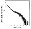
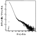
- FIG. 1 Energy wave height distribution when 0.66 MeV gamma ray from a 137 Cs source is detected using the radiation detector comprising the scintillator (Lu X0.997 Yb 0.003 ) 2 O 3 and a photomultiplier tube of Example 1.
- FIG. 1 Using the radiation detector comprising the scintillator (Lu X0.997 Yb 0.003 ) 2 O 3 and a photomultiplier tube of Example 1, the energy wave height distribution when detecting 0.66 MeV ⁇ -rays from a 137 Cs radiation source is shown.
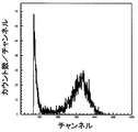
- FIG. 1 Using the radiation detector comprising the scintillator (Lu X0.997 Yb 0.003 ) 2 O 3 and an avalanche photodiode of Example 1, the energy wave height distribution when detecting 0.66 MeV ⁇ -rays from a 137 Cs radiation source is shown.
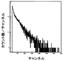
- the radiation detector comprising the scintillator (Lu X0.997 Yb 0.003 ) 2 O 3 and an avalanche photodiode of Example 1
- the energy wave height distribution when detecting 1.8 MeV ⁇ -ray from a 90 Sr radiation source is shown.
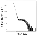
- FIG. Using the scintillator of Example 1 (Lu X0.997 Yb 0.003 ) 2 O 3 and an avalanche photodiode, the energy wave height distribution when detecting 5.5 MeV ⁇ -ray from a 241 Am radiation source is shown.
- FIG. 1 Energy wave height when detecting 1.8 MeV ⁇ -ray from 90 Sr source using radiation detector comprising scintillator (Lu X0.997 Yb 0.003 ) 2 O 3 and Geiger mode avalanche photodiode of Example 1 It is a figure which shows distribution.
- Micro pulling device 2 Melt 3: Crucible 3a: Fine pore 4: Seed crystal holding unit 4a: Seed crystal 5: Moving mechanism unit 5a: Pulling shaft 5b: Moving mechanism 5c: Moving mechanism control unit 6: Induction heating unit 6a: induction heating coil 7: furnace material 7a: heat insulating material 7b: after heater 8: crystal synthesis chamber 8a: vacuum exhaust unit 8b: gas introduction unit 9: single crystal 10: radiation detector 12: chamber 13: scintillator 14: light reception Element 14a: Power connection terminal 14b: Output terminal 15: Reflector 17: Read circuit 20, 20a: Radiation inspection apparatus 22: Bias power supply 23: Preamplifier 24: Waveform shaping amplifier 25: Multichannel analyzer 26: Computer 30: Radiation source 31: Image intensifier (IIT) 32: CCD 33: Read circuit 34: High voltage power supply
- the light-emitting material for scintillator has a chemical formula (R 1-X Yb X ) 2 O 3 (where R is selected from rare earth elements composed of Sc, Y and lanthanoids). It is a transparent ceramic represented by 0 ⁇ x ⁇ 0.1. Lanthanoids are elements having element numbers 57 to 71.
- the composition x of Yb serving as the emission center is set to be larger than 0 so that Yb is the emission center, and the upper limit is set to x ⁇ 0.1. This is because, as will be described later, if the amount of CTS of Yb 3+ is too large, concentration quenching occurs and the light emission amount decreases.
- the light emitting material for scintillator of the present invention generates fluorescence having an emission peak wavelength in a wavelength region of about 300 to 600 nm when irradiated with radiation.
- the generation of this fluorescence is Yb which is an element that forms an optically active state called a charge transfer state (hereinafter referred to as CTS) with oxygen ions, which are adjacent negative ions in the light emitting material.
- CTS charge transfer state
- oxygen ions which are adjacent negative ions in the light emitting material.
- radiation refers to particles ( ⁇ rays, ⁇ rays, neutron rays, etc.) and photons ( ⁇ rays, X rays, etc.) having sufficient energy to ionize atoms and molecules.
- R is one or more elements selected from rare earth elements composed of Sc (scandium), Y (yttrium) and lanthanoids.
- Sc scandium
- Y yttrium
- lanthanoids Preferably, one or more elements selected from Sc, Y, La (lanthanum), Gd (gadolinium), Lu (lutetium) and the like can be used.
- the composition x of the chemical formula (R 1-X Yb X ) 2 O 3 is 0 ⁇ x ⁇ 0.006, more preferably 0.001 ⁇ x ⁇ 0.005 may be satisfied. It is not preferable that the composition x of Yb is less than 0.001 because the amount of light emission becomes low because the CTS of Yb 3+ serving as the emission center is too small. Conversely, the upper limit is set to a value that does not cause a decrease in the amount of light emission due to the concentration quenching of Yb 3+ .
- the composition x of Yb may be smaller than 0.006 or smaller than 0.005.
- the response speed is shorter than 1 ns.
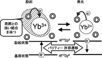
- FIG. 1 is a schematic diagram for explaining CTS by Yb ions contained in the light emitting material for scintillator of the present invention.
- Yb 3+ cations form an optically active state called CTS with oxygen ions, which are adjacent anions.
- the scintillator is irradiated with radiation, the Yb 3+ cation shown on the left side of FIG. 1 interacts with surrounding O, and the electron in the ground state 4f 13 2P 6 state is the excitation level 4f 14 excited to 2P 5, the fluorescence is emitted in the process of relaxation (see the right side in FIG. 1).
- Non-Patent Documents 1 and 2 which is a conventional additive for a scintillator luminescent material, forms an excited state of a 5d-4f transition in its nucleus.
- CTS formed by the interaction of Yb ions and O is not in the nucleus of Yb, but is in an excited state. The light emission accompanying the transition from this state.
- the fluorescence lifetime from CTS by Yb 3+ contained in the light emitting material for scintillator of the present invention is 100 to 300 ns at low temperature and 1 to 5 ns at room temperature.
- the fluorescence lifetime at room temperature from CTS by Yb 3+ is about one order of magnitude faster than the conventional Ce 3+ fluorescence lifetime of 10 to 80 ns.
- the wavelength range of fluorescence from CTS by Yb 3+ ranges from UV to red.
- the wavelength range of conventional Ce 3+ fluorescence is from UV to blue. From now on, since the fluorescence wavelength region from the light emitting material for scintillators of the present invention is wider than the conventional Ce 3+ fluorescence wavelength region and covers visible light up to red, various semiconductor detections described later are used for fluorescence detection. Can be used.
- the CTS with Yb 3+ has a large Stokes shift, whereas the conventional Ce 3+ has a small Stokes shift.
- the fluorescence lifetime at room temperature is shorter than 5 ns due to thermal quenching.
- the temperature dependence of the light emission amount depends on the composition other than Yb serving as the light emission center, that is, the host. For this reason, the fluorescence lifetime can be changed by combining with a host that exhibits a high light emission amount even at room temperature.
- Table 1 summarizes the comparison of fluorescence lifetime, fluorescence wavelength region, Stokes shift, and concentration quenching in the Yb 3+ CTS and Ce 3+ 5d-4f transitions according to the present invention.
- a sintered body or a single crystal made of polycrystal can be used as the scintillator light emitting material.
- a sintered body made of polycrystal is also simply called ceramics.
- a scintillator light-emitting material made of a polycrystalline sintered body can be produced by mixing raw materials, solidifying and firing this raw material powder.
- a single crystal of a scintillator luminescent material can be grown by a melt growth method such as the Bridgman method, the zone melt method, the Bernoulli method, the heat exchange method, the CZ method, the FZ method, or the micro-pulling down method.
- the polycrystal used as the raw material of the single crystal the same raw material as the polycrystal used as the light emitting material for the scintillator can be used.
- Each raw material powder of (R 1-X Yb X ) 2 O 3 includes an oxide of R And ytterbium oxide (Yb 2 O 3 ) which is an oxide of Yb can be used.
- the oxide of R include scandium oxide (Sc 2 O 3 ), yttrium oxide (Y 2 O 3 ), and lanthanoid oxides.
- lanthanoid oxides include lutetium oxide (Lu 2 O 3 ) and gadolinium oxide (Gd 2 O 3 ).
- Each raw material powder has a purity of 99.9% or more, a BET value (BET specific surface area) of 2 m 2 / g or more and 15 m 2 / g or less, and secondary aggregated particles exceeding 5 ⁇ m are 10% or less by mass fraction.
- This raw material powder is molded to form a raw material powder compact.
- This raw material powder compact is sintered at a temperature of 1750 ° C. or lower, which is extremely lower than the melting point, to synthesize a translucent sintered body. In order to make the average particle diameter of the translucent sintered body 20 ⁇ m or less, it is necessary to produce a high-density molded body.
- the raw material powder compact before sintering may have a compact density of 58% or more empirically after degreasing.
- the BET value of the raw material powder exceeds 15 m 2 / g, it is too fine to handle, and it is difficult to increase the density of the compact.
- the BET value of the raw material powder is less than 2 m 2 / g, it is not preferable because it is not easy to densify at a low temperature.
- the BET value of the raw material powder used is set to 2 m 2 / g or more and 15 m 2 / g or less.
- the BET value of the raw material powder is more preferably about 4 m 2 / g or more and 8 m 2 / g or less.
- a secondary agglomerated particle exceeding 5 ⁇ m is preferably a raw material powder having a mass fraction of 10% or less, preferably 5% or less, and a uniform particle size distribution.
- a high-density molded body cannot be obtained, which is not preferable.
- FIG. 2 is a schematic diagram showing the micro pull-down device 1.
- the micro-pulling device 1 includes a crucible 3 that holds a melt 2 and a seed crystal that holds a seed crystal 4 a that is brought into contact with the melt 2 flowing out from a pore 3 a provided at the bottom of the crucible 3.
- a holding unit 4, a moving mechanism unit 5 that moves the seed crystal holding unit 4 downward, and an induction heating unit 6 that heats the crucible 3 are provided.
- a heat insulating material 7 a made of zirconia or the like is disposed as the furnace material 7.
- the crucible 3 is accommodated in a crystal synthesis chamber 8 made of a quartz tube or the like disposed outside the heat insulating material 7.
- the crystal synthesis chamber 8 includes a vacuum exhaust unit 8a and a gas introduction unit 8b, and is a container that can be evacuated.
- the induction heating unit 6 that heats the crucible 3 includes an induction heating coil 6a that heats the crucible 3, an AC frequency power source (not shown) that supplies power to the induction heating coil 6a, and the like.
- the moving mechanism unit 5 includes a pulling shaft 5a that moves the seed crystal holding unit 4 downward, a moving mechanism 5b that moves the pulling shaft 5a in the vertical direction, and a moving mechanism control unit 5c.
- the moving mechanism control unit 5c performs position control of the pulling shaft 5a, speed control for moving the pulling shaft 5a downward during single crystal growth, and the like.
- An after heater 7b which is a heating element, is disposed on the outer periphery of the bottom of the crucible 3.
- the heating temperature of the solid-liquid boundary phase of the melt 2 drawn from the pores provided at the bottom of the crucible 3 is controlled by the crucible 3 and the after heater 7b heated by the induction heating coil 6a.
- the polycrystal of (R 1-X Yb X ) 2 O 3 described above is put in the crucible 3 as a raw material, and the crystal synthesis chamber 8 is evacuated by the vacuum exhaust part 8a, and then the gas introduction part 8b enters the crystal synthesis chamber 8
- An inert gas Ar is introduced to make the inside of the crystal synthesis chamber 8 an inert gas atmosphere.
- the inert gas Ar (85 to 99%) may be a mixed gas in which hydrogen gas (H 2 , 1 to 15%) is mixed to prevent the crucible 3 from being oxidized.
- the crucible 3 is heated by the induction heating coil 6a and the after heater 7b to completely melt the raw material in the crucible 3.
- the seed crystal 4a is gradually raised at a predetermined speed, and the tip of the seed crystal 4a is brought into contact with the pores at the lower end of the crucible 3 so that the seed crystal 4a is sufficiently adapted. Then, the single crystal 9 is grown by lowering the pulling shaft 5a while adjusting the melt temperature. When the melt 2 in the crucible 3 is all crystallized and the melt 2 is exhausted, the crystal growth is terminated.
- the micro-pulling device 1 When the micro-pulling device 1 is used, the effective segregation coefficient at the time of single crystallization from the melt is close to 1, and the light emitting material for scintillator is compared with the case of using the conventional pulling method or Bridgman method. There is an advantage that variation in composition is reduced. Compared with the conventional pulling method and Bridgman method, which requires a week to grow a single crystal of one composition, the micro pulling method has the advantage that it takes 5 to 10 hours. Can do growth.
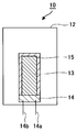
- FIG. 3 is a cross-sectional view showing the configuration of the radiation detector 10 according to the first exemplary embodiment of the present invention.
- the radiation detector 10 of the present invention includes a chamber 12, a scintillator 13 accommodated in the chamber 12, a light receiving element 14 that detects fluorescence from the scintillator 13, and a reflector 15. It is configured.
- the light receiving element 14 is provided in contact with the lower surface of the scintillator 13.
- the fluorescent material may be covered with a reflector 15 so that the fluorescence does not leak outside the scintillator 13.
- the light receiving element 14 includes a power connection terminal 14a to which power is supplied and an output terminal 14b.
- the light receiving element 14 converts the fluorescence emitted from the scintillator 13 made of (R 1 ⁇ X Yb X ) 2 O 3 into an electrical signal.
- the material of the scintillator 13 made of (R 1-X Yb X ) 2 O 3 is also called Yb mixed crystal rare earth oxide.
- the light receiving element 14 is preferably capable of detecting the emission peak wavelength of the scintillator 13, that is, the wavelength region of 300 to 600 nm, and has high quantum conversion efficiency.
- the quantum conversion efficiency is preferably 10% or more.
- a photomultiplier tube PMT
- PD photodiode
- APD avalanche photodiode
- IIT image intensifier
- a charge coupled device also referred to as a charge coupled device or CCD
- Examples of commercially available products that can be used for the light receiving element 14 include photomultiplier tubes, photodiodes, avalanche photodiodes, Geiger mode avalanche photodiodes manufactured by Hamamatsu Photonics Co., Ltd., and the like. Each of these light receiving elements 14 can detect a wavelength region of 200 nm to 900 nm, and has a quantum conversion efficiency of 10% or more in a wavelength region of 300 nm to 600 nm.
- the Yb mixed crystal rare earth oxide scintillator 13 has a fluorescence lifetime of 0.05 ns to 5 ns seconds due to light emission resulting from the transition from the charge transfer state (CTS) of Yb 3+ .
- the scintillator 13 made of Yb mixed crystal rare earth oxide has an emission peak wavelength in the range of 300 nm to 600 nm.
- the operation of the radiation detector 10 will be described.
- the radiation detector 10 when the radiation enters the Yb mixed crystal rare earth oxide scintillator 13, the Yb mixed crystal rare earth oxide scintillator 13 emits fluorescence, and the light receiving element 14 detects this fluorescence and converts it into an electrical signal. Output.
- both the Yb mixed crystal rare earth oxide scintillator 13 and the light receiving element 14 have high-speed response in the sub-nanosecond range of 0.05 ns to 1 ns. Furthermore, since the Yb mixed crystal rare earth oxide scintillator 13 contains an element having a high effective atomic number Z eff such as Lu as a constituent element of the mother crystal structure, it can detect radiation with high sensitivity and high accuracy. For this reason, the time resolution of the radiation detector 10 is also increased. Thereby, the radiation detector 10 has high time resolution and can prevent pile-up. For this reason, counting down decreases.
- FIG. 4 is a block diagram showing the configuration of the radiation inspection apparatus 20 according to the second embodiment of the present invention.
- the radiation inspection apparatus 20 of the present invention includes the radiation detector 10 described above, a bias power source 22, a preamplifier 23, a waveform shaping amplifier 24, a multichannel analyzer 25, a computer 26, and a radiation detector. And a radiation source 30.
- the bias power source 22 is connected to the power connection terminal 14 a of the light receiving element 14 in order to supply power to the radiation detector 10.
- the preamplifier 23 is connected to the output terminal 14b of the light receiving element 14, and amplifies the electric signal output from the light receiving element 14.
- the waveform shaping amplifier 24 is connected to the preamplifier 23, and shapes and further amplifies the signal waveform output from the preamplifier 23.
- the multi-channel analyzer 25 is connected to the waveform shaping amplifier 24 and receives a signal from the waveform shaping amplifier 24 to perform sampling, data storage, data display, and the like.
- a computer such as a personal computer (PC) can be used as the computer 26.
- the computer 26 is connected to the multi-channel analyzer 25 and can execute various arithmetic processes on the measurement data. Thereby, the radiation inspection apparatus 20 can detect the radiation from the radiation source 30 with the radiation detector 10, can preserve
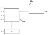
- FIG. 5 is a block diagram showing a configuration of a modification of the radiation inspection apparatus 20 according to the second embodiment of the present invention.
- the radiation inspection apparatus 20 a of the present invention uses the light receiving element 14 of the radiation detector 10 as an image intensifier (IIT) 31, and further receives the output light from the image intensifier 31 by the CCD 32.
- the readout circuit 33 for reading out the output from the CCD 32 is outputted to the personal computer 26.
- a high voltage power supply 34 is connected to the image intensifier 31 as a bias power supply.
- the readout circuit 33 includes an amplifier, an A / D converter that converts an amplified analog signal into a digital signal, and the like.
- the radiation inspection apparatuses 20 and 20a can configure, for example, PET, X-ray CT, SPECT (single photon emission tomography), etc., depending on the radiation source 30 used.
- the radiation inspection apparatuses 20 and 20a are not particularly limited when made of PET, but are MRI-PET, CT-PET, two-dimensional PET, three-dimensional PET, time-of-flight positron emission apparatus (TOF type PET). It is preferably made of depth detection (DOI) type PET, OPEN-PET. Furthermore, the radiation inspection apparatuses 20 and 20a may be configured by a combination of these.
- TOF type PET which is currently expected to be realized, differs from the conventional two scintillators, that is, a method of detecting with equal probability on a straight line (LOR) connecting both detectors.
- the coordinate point of the radiation source 30 is obtained from the difference in measurement time, and the distribution blurred with a Gaussian function corresponding to the time resolution of the detector along the LOR is used as position information. For this reason, the response speed of the conventional scintillator has a position identification capability of less than 100 cm.
- the fluorescence lifetime of the scintillator 13 is about an order of magnitude faster than that of the conventional scintillator.
- a position identification capability of several centimeters can be provided, and high performance can be achieved.
- the radiation inspection apparatus 20 includes the radiation detector 10 having a high-speed response, the data acquisition time can be greatly shortened. For this reason, by using the radiation inspection apparatus 20 for a medical imaging apparatus or the like, the inspection time can be shortened, and the burden on the subject can be greatly reduced.
- the present invention will be described in more detail by way of examples.
- a high-purity lutetium chloride solution Shin-Etsu Chemical Co., Ltd.
- a lutetium chloride aqueous solution 2 liters of an ammonium hydrogen carbonate solution having a concentration of 3 M (mol ⁇ dm ⁇ 3 ) was dropped at a rate of 5 ml per minute, followed by stirring and curing at room temperature for 7 days. After curing, filtration and washing with ultrapure water were repeated several times, and then put into a dryer at 150 ° C. and dried for 3 days to prepare a precursor powder. The obtained precursor powder was put into an alumina crucible and calcined in an electric furnace at 1200 ° C. for 10 hours, whereby lutetium oxide having a BET specific surface area value of 5.0 m 2 / g and an average primary particle size of 0.13 ⁇ m. Raw material powder was prepared.
- ytterbium oxide raw material powder manufactured by Shin-Etsu Chemical Co., Ltd., purity 99.99%, BET specific surface area value 2.7 m 2 / g
- BET specific surface area value 2.7 m 2 / g BET specific surface area value 2.7 m 2 / g
- 2 g of Kyoeisha Chemical's Floren G700 (Floren is a trade name of Kyoeisha Chemical) and 0.5 g of Sekisui Chemical's PVB-BL1 (PVB-BL1 is a trade name of Sekisui Chemical) were added as a binder.
- Ethanol 35g was added to this mixture, and it mixed for 50 hours using the nylon pot and the nylon ball, and was set as the alcohol slurry.
- the molded article was produced by pouring the alcohol slurry into a gypsum mold and curing for 3 days.
- the amount of the ytterbium oxide raw material powder may be adjusted.
- x is 0.01, the amount of the ytterbium oxide raw material powder is set to 0.99 g.
- the molded body was heated at 5 ° C./hour in an oxygen stream, and degreased at 900 ° C. for 40 hours.
- the composition ratio of the compact was determined by ICP (inductively coupled plasma) emission spectrometry, and was (Lu 0.997 Yb 0.003 ) 2 O 3 .
- the compact was further heated to 1200 ° C. and held for 10 hours. Then, it sintered for 10 hours at the temperature of 1650 degreeC in the vacuum baking furnace. At this time, the heating rate was 300 ° C./hour up to 1200 ° C., 50 ° C./hour above that, and the degree of vacuum in the furnace was 10 ⁇ 2 Pa or less.
- the obtained sintered body was annealed in the atmosphere at 900 ° C. for 50 hours, and then mirror-polished using a diamond slurry to produce a transparent polycrystalline ceramic.
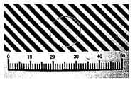
- FIG. 6 is an optical image showing the transparency of the scintillator crystal made of (Lu X0.99 Yb 0.01 ) 2 O 3 in Example 1. As is apparent from FIG. 6, since the pattern below the scintillator crystal made of (Lu X0.99 Yb 0.01 ) 2 O 3 of Example 1 is seen through, it can be seen that the scintillator crystal is highly transparent.
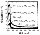
- FIG. 7 also shows Lu 2 O 3 data to which Yb is not added for comparison. As is apparent from FIG. 7, it can be seen that there is no absorption in the vicinity of 300 to 530 nm, which is the emission peak due to the transition from the charge transfer state (CTS) of Yb 3+ .
- CTS charge transfer state
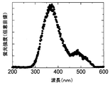
- the horizontal axis represents wavelength (nm) and the vertical axis represents fluorescence intensity (arbitrary scale).
- the fluorescence intensity spectrum has two peaks characteristic of the emission peak caused by the transition from the charge transfer state (CTS) of Yb 3+ at around 370 nm and around 480 nm. I understand that.
- CTS charge transfer state
- the horizontal axis of FIG. 9 is time (ns), and the vertical axis is the fluorescence count.
- these scintillators 13 have an extremely short sub-nanosecond fluorescence lifetime of 0.8 ns.
- the scintillator 13 made of (Lu X0.99 Yb 0.01 ) 2 O 3 has a light emission amount of about 1000 photons / MeV.
- the radiation detector 10 was manufactured.
- the reflecting member 14 covering the scintillator 13 a fluororesin tape was used.
- the light receiving element 14 a photomultiplier tube, an avalanche photodiode, or a Geiger mode avalanche photodiode was used.
- the radiation detector 10 has a light emission amount of about 1000 photons / MeV when a photomultiplier tube is used as the light receiving element 14.
- a radiation inspection apparatus 20 was manufactured using the radiation detector 10 of Example 2.
- the radiation inspection apparatus 20 has the configuration shown in FIG.
- a radiation source 30 a ⁇ ray having an energy of 0.66 MeV from a 137 Cs source, a ⁇ ray having an energy of 1.8 MeV from a 90 Sr source, and a 241 Am source ⁇ rays with an energy of 5.5 MeV were used.
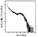
- FIG. 10 shows detection of 0.66 MeV ⁇ rays from a 137 Cs source using the radiation detector 10 comprising the scintillator 13 (Lu X0.997 Yb 0.003 ) 2 O 3 and a photomultiplier tube of Example 1. It is a figure which shows energy wave height distribution at the time of doing.
- the horizontal axis in FIG. 10 is the channel, and the vertical axis is the fluorescence count in each channel.
- the display in FIGS. 11 to 17 described later is also the same.
- the radiation detector 10 was able to detect 0.66 MeV ⁇ rays from a 137 Cs radiation source with high sensitivity by using a photomultiplier tube as the light receiving element 14.
- FIG. 11 shows detection of 1.8 MeV ⁇ -rays from a 90 Sr source using the radiation detector 10 comprising the scintillator 13 (Lu X0.997 Yb 0.003 ) 2 O 3 and a photomultiplier tube of Example 1. It is a figure which shows energy wave height distribution at the time of doing. As shown in FIG. 11, the radiation detector 10 was able to detect the 1.8 MeV ⁇ -ray from the 90 Sr radiation source with high sensitivity using a photomultiplier tube as the light receiving element 14.
- FIG. 12 shows detection of 5.5 MeV ⁇ -rays from a 241 Am radiation source using the radiation detector 10 composed of the scintillator 13 (Lu X0.997 Yb 0.003 ) 2 O 3 and a photomultiplier tube of Example 1. It is a figure which shows energy wave height distribution at the time of doing. As shown in FIG. 12, the radiation detector 10 was able to detect 5.5 MeV ⁇ rays from a 241 Am radiation source with high sensitivity by using a photomultiplier tube as the light receiving element 14.
- FIG. 13 shows the detection of 0.66 MeV ⁇ rays from a 137 Cs source using the radiation detector 10 comprising the scintillator 13 (Lu X0.997 Yb 0.003 ) 2 O 3 and an avalanche photodiode in Example 1. It is a figure which shows energy wave height distribution at the time.
- the ⁇ -ray signal is shown by a straight line, and the gentle slope in the figure is a ⁇ -ray direct detection signal by an avalanche photodiode.
- the radiation detector 10 was able to detect 0.66 MeV ⁇ rays from a 137 Cs radiation source with high sensitivity by using an avalanche photodiode as the light receiving element 14.
- FIG. 14 shows detection of 1.8 MeV ⁇ -rays from a 90 Sr radiation source using the radiation detector 10 composed of the scintillator 13 (Lu X0.997 Yb 0.003 ) 2 O 3 of Example 1 and an avalanche photodiode. It is a figure which shows energy wave height distribution at the time. As shown in FIG. 14, the radiation detector 10 was able to detect the 1.8 MeV ⁇ -ray from the 90 Sr radiation source with high sensitivity by using an avalanche photodiode as the light receiving element 14.
- FIG. 15 shows detection of 5.5 MeV ⁇ rays from a 241 Am radiation source using the radiation detector 10 comprising the scintillator 13 (Lu X0.997 Yb 0.003 ) 2 O 3 of Example 1 and an avalanche photodiode. It is a figure which shows energy wave height distribution at the time.
- the radiation detector 10 can detect the 5.5 MeV ⁇ ray from the 241 Am radiation source with high sensitivity by using an avalanche photodiode as the light receiving element 14.
- FIG. 16 shows a 5.5 MeV ⁇ ray from a 241 Am radiation source using the radiation detector 10 composed of the scintillator 13 (Lu X0.997 Yb 0.003 ) 2 O 3 and Geiger mode avalanche photodiode of Example 1. The energy wave height distribution at the time of detection is shown.
- the radiation detector 10 was able to detect the 5.5 MeV ⁇ ray from the 241 Am radiation source with high sensitivity by using a Geiger mode avalanche photodiode as the light receiving element 14.
- FIG. 17 shows a 1.8 MeV ⁇ ray from a 90 Sr radiation source using the radiation detector 10 composed of the scintillator 13 (Lu X0.997 Yb 0.003 ) 2 O 3 and Geiger mode avalanche photodiode of Example 1. The energy wave height distribution at the time of detection is shown.
- the radiation detector 10 was able to detect the 1.8 MeV ⁇ -ray from the 90 Sr radiation source with high sensitivity by using a Geiger mode avalanche photodiode as the light receiving element 14.
- the characteristics of the radiation detector 10 were the same even if the light receiving element 14 was replaced with IIT and CCD. From the above measurement, in the scintillator 13 (Lu X0.997 Yb 0.003 ) 2 O 3 of Example 1, the light receiving peak wavelength is 360 to 370 nm, the light emission amount is 1500 photons / MeV, and the fluorescence lifetime is about 1 ns. there were.
- Example 4 a fluorescent material having a blending ratio of (Lu 0.99 Sc 0.007 Yb 0.003 ) 2 O 3 was produced.
- Lutetium oxide raw material powder and ytterbium oxide raw material powder manufactured by Shin-Etsu Chemical Co., Ltd., purity 99.99%, BET specific surface area value 2.7 m 2 / g) prepared in Example 1 and scandium oxide raw material powder (Shin-Etsu Chemical Co., Ltd.) Co., Ltd., purity 99.99%, BET specific surface area value 3.5 m 2 / g) was weighed so as to have a composition ratio of (Lu 0.99 Sc 0.007 Yb 0.003 ) 2 O 3 , and then mixed to prepare a raw material A mixed powder was obtained.
- the raw material mixed powder was treated in the same manner as in Example 1 and vacuum baked at 1650 ° C. for 10 hours to obtain a transparent polycrystalline ceramic composed of (Lu 0.99 Sc 0.007 Yb 0.003 ) 2 O 3 of Example 4. Produced. Next, a radiation detector 10 using this transparent polycrystalline ceramic was manufactured. The radiation detector 10 was incorporated in the radiation inspection apparatus 20, and the characteristics of the scintillator 13 were measured in the same manner as in Example 3.
- the light reception peak wavelength was 360 to 370 nm
- the light emission amount when irradiated with ⁇ rays was 1800 photons / MeV
- the fluorescence lifetime was about 1.5 ns.
- Example 5 a fluorescent material having a blending ratio of (Lu 0.99 Y 0.007 Yb 0.003 ) 2 O 3 was produced.
- the lutetium oxide raw material powder and the yttrium oxide raw material powder (manufactured by Shin-Etsu Chemical Co., Ltd., purity 99.99%, BET specific surface area value 4.5 m 2 / g) prepared in Example 1 and the ytterbium oxide raw material powder (Shin-Etsu Chemical Co., Ltd.) Co., Ltd., purity 99.99%, BET specific surface area value 2.7 m 2 / g) was weighed so as to have a composition ratio of (Lu 0.99 Y 0.007 Yb 0.003 ) 2 O 3 , then mixed and used as a raw material A mixed powder was obtained.
- the raw material mixed powder was treated in the same manner as in Example 1 and vacuum baked at 1650 ° C. for 10 hours to obtain a transparent polycrystalline ceramic composed of (Lu 0.99 Y 0.007 Yb 0.003 ) 2 O 3 of Example 5. Produced. Next, a radiation detector 10 using this transparent polycrystalline ceramic was manufactured. The radiation detector 10 was incorporated in the radiation inspection apparatus 20, and the characteristics of the scintillator 13 were measured in the same manner as in Example 3.
- the light receiving peak wavelength was 360 to 370 nm
- the light emission amount was 1400 photons / MeV
- the fluorescence lifetime was about 1 ns.
- Example 6 a fluorescent material having a blending ratio of (Lu 0.99 Gd 0.007 Yb 0.003 ) 2 O 3 was produced.
- Lutetium oxide raw material powder and ytterbium oxide raw material powder manufactured by Shin-Etsu Chemical Co., Ltd., purity 99.99%, BET specific surface area value 2.7 m 2 / g) and gadolinium oxide raw material powder (Shin-Etsu Chemical Co., Ltd.) prepared in Example 1 (Made by Co., Ltd., purity 99.99%, BET specific surface area value 4.3 m 2 / g) was weighed so as to have a composition ratio of (Lu 0.99 Gd 0.007 Yb 0.003 ) 2 O 3 , then mixed and used as a raw material A mixed powder was obtained.
- This raw material mixed powder was treated in the same manner as in Example 1 and vacuum baked at 1650 ° C. for 10 hours to produce scintillator 13 made of (Lu 0.99 Gd 0.007 Yb 0.003 ) 2 O 3 of Example 6.
- the radiation detector 10 using this scintillator 13 was manufactured.
- the radiation detector 10 was incorporated in the radiation inspection apparatus 20, and the characteristics of the scintillator 13 were measured in the same manner as in Example 3.
- the light receiving peak wavelength was 360 to 370 nm
- the light emission amount was 1500 photons / MeV
- the fluorescence lifetime was about 1.5 ns.
- Example 7 a fluorescent material having a blending ratio of (Lu 0.99 La 0.007 Yb 0.003 ) 2 O 3 was produced.
- the lutetium oxide raw material powder and the lanthanum oxide raw material powder (manufactured by Shin-Etsu Chemical Co., Ltd., purity 99.99%, BET specific surface area value 3.8 m 2 / g) prepared in Example 1 and ytterbium oxide raw material powder (Shin-Etsu Chemical Co., Ltd.) Co., Ltd., purity 99.99%, BET specific surface area value 2.7 m 2 / g) was weighed so as to have a composition ratio of (Lu 0.99 La 0.007 Yb 0.003 ) 2 O 3 , and then mixed to prepare a raw material A mixed powder was obtained.
- This raw material mixed powder was treated in the same manner as in Example 1 and vacuum baked at 1650 ° C. for 10 hours to produce scintillator 13 made of (Lu 0.99 La 0.007 Yb 0.003 ) 2 O 3 of Example 6.
- the radiation detector 10 using this scintillator 13 was manufactured.
- the radiation detector 10 was incorporated in the radiation inspection apparatus 20, and the characteristics of the scintillator 13 were measured in the same manner as in Example 3.
- the light receiving peak wavelength was 360 to 370 nm
- the light emission amount was 1000 photons / MeV
- the fluorescence lifetime was about 1.5 ns.
- Example 8 a fluorescent material having a compounding ratio of (Lu 0.99 Sc 0.003 Y 0.004 Yb 0.003 ) 2 O 3 was produced.
- the lutetium oxide raw material powder and scandium oxide raw material powder (manufactured by Shin-Etsu Chemical Co., Ltd., purity 99.99%, BET specific surface area value 3.5 m 2 / g) prepared in Example 1 and yttrium oxide raw material powder (Shin-Etsu Chemical Co., Ltd.) Manufactured by Co., Ltd., purity 99.99%, BET specific surface area value 4.5 m 2 / g) and ytterbium oxide raw material powder (manufactured by Shin-Etsu Chemical Co., Ltd., purity 99.99%, BET specific surface area value 2.7 m 2) / G) was weighed so as to have a composition ratio of (Lu 0.99 Sc 0.003 Y 0.004 Yb 0.003 ) 2 O 3 and then mixed to
- the raw material mixed powder is treated in the same manner as in Example 1 and vacuum baked at 1650 ° C. for 10 hours to produce the scintillator 13 made of (Lu 0.99 Sc 0.003 Y 0.004 Yb 0.003 ) 2 O 3 of Example 6. did.
- the radiation detector 10 using this scintillator 13 was manufactured.
- the radiation detector 10 was incorporated in the radiation inspection apparatus 20, and the characteristics of the scintillator 13 were measured in the same manner as in Example 3.
- the light receiving peak wavelength was 360 to 370 nm
- the light emission amount was 1700 photons / MeV
- the fluorescence lifetime was about 1.5 ns.
- Example 9 a fluorescent material having a blending ratio of (Lu 0.99 Sc 0.003 Gd 0.004 Yb 0.003 ) 2 O 3 was produced.
- Lutetium oxide raw material powder and scandium oxide raw material powder (manufactured by Shin-Etsu Chemical Co., Ltd., purity 99.99%, BET specific surface area value 3.5 m 2 / g) and gadolinium oxide raw material powder (Shin-Etsu Chemical Co., Ltd.) produced in Example 1 Manufactured by Co., Ltd., purity 99.99%, BET specific surface area value 4.3 m 2 / g) and ytterbium oxide raw material powder (manufactured by Shin-Etsu Chemical Co., Ltd., purity 99.99%, BET specific surface area value 2.7 m 2) / G) was weighed so as to have a composition ratio of (Lu 0.99 Sc 0.003 Gd 0.004 Yb 0.003 ) 2 O 3 and mixed to obtain a
- the raw material mixed powder is treated in the same manner as in Example 1 and vacuum baked at 1650 ° C. for 10 hours to produce the scintillator 13 made of (Lu 0.99 Sc 0.003 Gd 0.004 Yb 0.003 ) 2 O 3 of Example 9. did.
- the radiation detector 10 using this scintillator 13 was manufactured.
- the radiation detector 10 was incorporated in the radiation inspection apparatus 20, and the characteristics of the scintillator 13 were measured in the same manner as in Example 3.
- the light receiving peak wavelength was 360 to 370 nm
- the light emission amount was 1600 photons / MeV
- the fluorescence lifetime was about 1.5 ns.
- Example 10 a fluorescent material having a blending ratio of (Lu 0.99 Sc 0.005 La 0.002 Yb 0.003 ) 2 O 3 was produced.
- Lutetium oxide raw material powder and scandium oxide raw material powder (manufactured by Shin-Etsu Chemical Co., Ltd., purity 99.99%, BET specific surface area value 3.5 m 2 / g) and lanthanum oxide raw material powder (Shin-Etsu Chemical Industry) produced in Example 1 Manufactured by Co., Ltd., purity 99.99%, BET specific surface area value 3.8 m 2 / g) and ytterbium oxide raw material powder (manufactured by Shin-Etsu Chemical Co., Ltd., purity 99.99%, BET specific surface area value 2.7 m 2) / G) was weighed so as to have a composition ratio of (Lu 0.99 Sc 0.005 La 0.002 Yb 0.003 ) 2 O 3 and mixed to obtain a raw material mixed powder.
- This raw material mixed powder is treated in the same manner as in Example 1 and vacuum baked at 1650 ° C. for 10 hours to produce the scintillator 13 made of (Lu 0.99 Sc 0.005 La 0.002 Yb 0.003 ) 2 O 3 of Example 10. did.
- the radiation detector 10 using this scintillator 13 was manufactured.
- the radiation detector 10 was incorporated in the radiation inspection apparatus 20, and the characteristics of the scintillator 13 were measured in the same manner as in Example 3.
- the light receiving peak wavelength was 360 to 370 nm
- the light emission amount was 1400 photons / MeV
- the fluorescence lifetime was about 1.7 ns.
- Example 11 a fluorescent material having a blending ratio of (Lu 0.99 Y 0.004 Gd 0.003 Yb 0.003 ) 2 O 3 was produced.
- the lutetium oxide raw material powder and yttrium oxide raw material powder (manufactured by Shin-Etsu Chemical Co., Ltd., purity 99.99%, BET specific surface area value 4.5 m 2 / g) and gadolinium oxide raw material powder (Shin-Etsu Chemical Industry) produced in Example 1 Manufactured by Co., Ltd., purity 99.99%, BET specific surface area value 4.3 m 2 / g) and ytterbium oxide raw material powder (manufactured by Shin-Etsu Chemical Co., Ltd., purity 99.99%, BET specific surface area value 2.7 m 2) / G) was weighed so as to have a composition ratio of (Lu 0.99 Y 0.004 Gd 0.003 Yb 0.003 ) 2 O 3 and then mixed to
- the raw material mixed powder is treated in the same manner as in Example 1 and vacuum baked at 1650 ° C. for 10 hours to produce the scintillator 13 made of (Lu 0.99 Y 0.004 Gd 0.003 Yb 0.003 ) 2 O 3 of Example 11. did.
- the radiation detector 10 using this scintillator 13 was manufactured.
- the radiation detector 10 was incorporated in the radiation inspection apparatus 20, and the characteristics of the scintillator 13 were measured in the same manner as in Example 3.
- the light receiving peak wavelength was 360 to 370 nm
- the light emission amount was 1500 photons / MeV
- the fluorescence lifetime was about 1 ns.
- Example 12 a fluorescent material having a blending ratio of (Lu 0.99 Y 0.005 La 0.02 Yb 0.003 ) 2 O 3 was produced.
- the lutetium oxide raw material powder and the yttrium oxide raw material powder (manufactured by Shin-Etsu Chemical Co., Ltd., purity 99.99%, BET specific surface area value 4.5 m 2 / g) and lanthanum oxide raw material powder (Shin-Etsu Chemical Industry) produced in Example 1 Manufactured by Co., Ltd., purity 99.99%, BET specific surface area value 3.8 m 2 / g) and ytterbium oxide raw material powder (manufactured by Shin-Etsu Chemical Co., Ltd., purity 99.99%, BET specific surface area value 2.7 m 2) / G) was weighed so as to have a composition ratio of (Lu 0.99 Y 0.005 La 0.02 Yb 0.003 ) 2 O 3 and mixed to obtain a raw
- This raw material mixed powder is treated in the same manner as in Example 1 and vacuum baked at 1650 ° C. for 10 hours to produce the scintillator 13 made of (Lu 0.99 Y 0.005 La 0.02 Yb 0.003 ) 2 O 3 of Example 12. did.
- the radiation detector 10 using this scintillator 13 was manufactured.
- the radiation detector 10 was incorporated in the radiation inspection apparatus 20, and the characteristics of the scintillator 13 were measured in the same manner as in Example 3.
- the light receiving peak wavelength was 360 to 370 nm
- the light emission amount was 1400 photons / MeV
- the fluorescence lifetime was about 1 ns.
- Example 13 a fluorescent material having a blending ratio of (Lu 0.99 Gd 0.005 La 0.002 Yb 0.003 ) 2 O 3 was produced.
- the lutetium oxide raw material powder and gadolinium oxide raw material powder (manufactured by Shin-Etsu Chemical Co., Ltd., purity 99.99%, BET specific surface area value 4.3 m 2 / g) and lanthanum oxide raw material powder (Shin-Etsu Chemical Industry) produced in Example 1 Manufactured by Co., Ltd., purity 99.99%, BET specific surface area value 3.8 m 2 / g) and ytterbium oxide raw material powder (manufactured by Shin-Etsu Chemical Co., Ltd., purity 99.99%, BET specific surface area value 2.7 m 2) / G) was weighed so as to have a composition ratio of (Lu 0.99 Gd 0.005 La 0.002 Yb 0.003 ) 2 O 3 and mixed to obtain a raw
- This raw material mixed powder is treated in the same manner as in Example 1 and vacuum baked at 1650 ° C. for 10 hours to produce the scintillator 13 made of (Lu 0.99 Gd 0.005 La 0.002 Yb 0.003 ) 2 O 3 of Example 13. did.
- the radiation detector 10 using this scintillator 13 was manufactured.
- the radiation detector 10 was incorporated in the radiation inspection apparatus 20, and the characteristics of the scintillator 13 were measured in the same manner as in Example 3.
- the light receiving peak wavelength was 360 to 370 nm
- the light emission amount was 1500 photons / MeV
- the fluorescence lifetime was about 1 ns.
- Table 2 summarizes the emission peak wavelength, emission amount, and fluorescence lifetime when the radiation detector 10 using the scintillators 13 of Examples 3 to 13 is irradiated with ⁇ rays.
- Example 14 a fluorescent material having a blending ratio of (Gd 0.997 Yb 0.003 ) 2 O 3 was produced.
- the single crystal for the scintillator 13 was produced using a micro pulling method.
- As the melt a mixture of oxide powders of Gd 2 O 3 and Yb 2 O 3 so that the single crystal has a composition ratio of (Gd 0.997 Yb 0.003 ) 2 O 3 was used. That is, an oxide powder raw material having a purity of 99.99% was prepared, and Re metal was used as a crucible.
- As the atmosphere a mixed gas composed of Ar (97%) gas and H 2 (3%) gas was used.
- a single crystal having the same composition as the single crystal to be produced was cut in the [111] direction to obtain a seed crystal.
- the solid-liquid interface was observed with a CCD camera to determine the appropriate temperature and crystal production rate.
- a typical condition for the crystal production speed was 0.05 to 0.1 mm / min.
- the radiation detector 10 using the scintillator 13 made of (Gd 0.997 Yb 0.003 ) 2 O 3 was manufactured and incorporated in the radiation inspection apparatus 20, and the characteristics of the scintillator 13 were measured in the same manner as in Example 3.
- the light reception peak wavelength was 360 to 370 nm
- the light emission amount was 1600 photons / MeV
- the fluorescence lifetime was about 1 ns.
- Lu in Example 3 is replaced with Gd, but the received light peak wavelength is 360 to 370 nm as in Example 3.
- the light emission amount and fluorescence lifetime of Example 14 were the same as those of Example 3.
- Example 15 a fluorescent material having a blending ratio of (Gd 0.947 Sc 0.05 Yb 0.003 ) 2 O 3 was produced.
- the radiation detector 10 using the scintillator 13 made of (Gd 0.947 Sc 0.05 Yb 0.003 ) 2 O 3 is manufactured in the same manner as in the fourteenth embodiment, and is incorporated in the radiation inspection apparatus 20.
- the characteristics of the scintillator 13 were measured.
- the received light peak wavelength was 360 to 370 nm
- the light emission amount was 1800 photons / MeV
- the fluorescence lifetime was about 1.5 ns.
- Example 16 a fluorescent material having a blending ratio of (Gd 0.947 Y 0.05 Yb 0.003 ) 2 O 3 was produced.
- the radiation detector 10 using the scintillator 13 made of (Gd 0.947 Y 0.05 Yb 0.003 ) 2 O 3 is manufactured in the same manner as in the fourteenth embodiment, incorporated in the radiation inspection apparatus 20, and the same as in the third embodiment. The characteristics of the scintillator 13 were measured.
- the light receiving peak wavelength was 360 to 370 nm
- the light emission amount was 1600 photons / MeV
- the fluorescence lifetime was about 1 ns.
- Example 17 a fluorescent material having a blending ratio of (Gd 0.947 La 0.05 Yb 0.003 ) 2 O 3 was produced.
- the radiation detector 10 using the scintillator 13 made of (Gd 0.947 La 0.05 Yb 0.003 ) 2 O 3 is manufactured and incorporated in the radiation inspection apparatus 20, and the same as in Example 3.
- the characteristics of the scintillator 13 were measured.
- the light reception peak wavelength was 360 to 370 nm
- the light emission amount was 1200 photons / MeV
- the fluorescence lifetime was about 1 ns.
- Table 3 summarizes the emission peak wavelength, emission amount, and fluorescence lifetime when the radiation detector 10 using the scintillators 13 of Examples 14 to 17 is irradiated with ⁇ rays.
- Example 18 a fluorescent material with a blending ratio of (La 0.997 Yb 0.003 ) 2 O 3 was produced.
- polycrystal was used as in Example 1.
- the radiation detector 10 using the scintillator 13 made of (La 0.997 Yb 0.003 ) 2 O 3 was manufactured, incorporated in the radiation inspection apparatus 20, and the characteristics of the scintillator 13 were measured in the same manner as in Example 3.
- the received light peak wavelength was 360 to 370 nm
- the light emission amount was 200 photons / MeV
- the fluorescence lifetime was about 1 ns.
- Example 14 Lu in Example 3 is replaced with La, but the received light peak wavelength is 360 to 370 nm as in Example 3. Further, the light emission amount of Example 14 was about 13% of Example 3, but the fluorescence lifetime was the same as that of Example 3.
- Example 19 a fluorescent material having a blending ratio of (La 0.947 Sc 0.05 Yb 0.003 ) 2 O 3 was produced.
- the radiation detector 10 using the scintillator 13 made of (La 0.947 Sc 0.05 Yb 0.003 ) 2 O 3 was manufactured and incorporated in the radiation inspection apparatus 20, and the characteristics of the scintillator 13 were measured in the same manner as in Example 3. did.
- the light receiving peak wavelength was 360 to 370 nm
- the light emission amount was 400 photons / MeV
- the fluorescence lifetime was about 1.5 ns.
- Example 20 a fluorescent material having a blending ratio of (La 0.947 Y 0.05 Yb 0.003 ) 2 O 3 was produced.
- the radiation detector 10 using the scintillator 13 made of (La 0.947 Y 0.05 Yb 0.003 ) 2 O 3 was manufactured and incorporated in the radiation inspection apparatus 20, and the characteristics of the scintillator 13 were measured in the same manner as in Example 3. did.
- the light reception peak wavelength was 360 to 370 nm
- the light emission amount was 300 photons / MeV
- the fluorescence lifetime was about 1 ns.
- Example 21 a fluorescent material having a blending ratio of (La 0.947 Gd 0.05 Yb 0.003 ) 2 O 3 was produced.
- the radiation detector 10 using the scintillator 13 made of (La 0.947 Gd 0.05 Yb 0.003 ) 2 O 3 was manufactured and incorporated in the radiation inspection apparatus 20, and the characteristics of the scintillator 13 were measured in the same manner as in Example 3. did.
- the light reception peak wavelength was 360 to 370 nm
- the light emission amount was 300 photons / MeV
- the fluorescence lifetime was about 1 ns.
- Table 4 summarizes the emission peak wavelength, emission amount, and fluorescence lifetime when the radiation detector 10 using the scintillators 13 of Examples 18 to 21 is irradiated with ⁇ rays.
- Example 22 a fluorescent material with a blending ratio of (Sc 0.997 Yb 0.003 ) 2 O 3 was produced.
- a scandium oxide raw material powder was produced (see Patent Document 2, paragraph [0040]). Scandium oxide having a purity of 99.9% or more and Si of 5 ppm was dissolved in hydrochloric acid to prepare an aqueous scandium chloride solution having a concentration of 0.25 M (mol ⁇ dm ⁇ 3 ). 500 ml of this solution was placed in a polytetrafluoroethylene beaker and stirred.
- a 0.5M (mol ⁇ dm ⁇ 3 ) ammonium hydrogen carbonate solution was dropped into an aqueous scandium chloride solution at a rate of 5 ml / min until pH 8.0 was reached, followed by curing at room temperature for 10 days. . After curing, filtration and washing with ultrapure water were repeated several times, and then placed in a dryer at 150 ° C. and dried for 2 days.
- the obtained precursor powder was put into an alumina crucible and calcined (1250 ° C. ⁇ 3 hours) in an electric furnace to prepare a scandium oxide raw material powder having an average primary particle size of 0.35 ⁇ m.
- the scandium oxide raw material powder and the ytterbium oxide raw material powder (manufactured by Shin-Etsu Chemical Co., Ltd., purity 99.99%, BET specific surface area value 2.7 m 2 / g) are (Sc 0.997 Yb 0.003 ) 2 O 3
- the raw material mixed powder was treated in the same manner as in Example 1 and vacuum baked at 1700 ° C. for 5 hours to produce a scintillator 13 made of (Sc 0.997 Yb 0.003 ) 2 O 3 of Example 22.
- the radiation detector 10 using this scintillator 13 was manufactured.
- the radiation detector 10 was incorporated in the radiation inspection apparatus 20, and the characteristics of the scintillator 13 were measured in the same manner as in Example 3.
- the light receiving peak wavelength was 360 to 370 nm
- the light emission amount was 2000 photons / MeV
- the fluorescence lifetime was about 2 ns.
- Lu in Example 3 is replaced with Sc, but the received light peak wavelength is 360 to 370 nm as in Example 3.
- the light emission amount of Example 22 was about 133% of Example 3, but the fluorescence lifetime was 2 ns, about twice that of Example 3.
- Example 23 a fluorescent material having a blending ratio of (Sc 0.99 Y 0.007 Yb 0.003 ) 2 O 3 was produced.
- Scandium oxide raw material powder and yttrium oxide raw material powder produced by Example 22 manufactured by Shin-Etsu Chemical Co., Ltd., purity 99.99%, BET specific surface area value 4.5 m 2 / g) and ytterbium oxide (Shin-Etsu Chemical Co., Ltd.) ), Purity 99.99%, BET specific surface area value 2.7 m 2 / g) was weighed so as to have a composition ratio of (Sc 0.99 Y 0.007 Yb 0.003 ) 2 O 3 , and mixed to mix the raw materials Powdered.
- the raw material mixed powder was treated in the same manner as in Example 1 and vacuum baked at 1700 ° C. for 5 hours to produce a scintillator 13 made of (Sc 0.99 Y 0.007 Yb 0.003 ) 2 O 3 of Example 23.
- the radiation detector 10 using this scintillator 13 was manufactured.
- the radiation detector 10 was incorporated in the radiation inspection apparatus 20, and the characteristics of the scintillator 13 were measured in the same manner as in Example 3.
- the light receiving peak wavelength was 360 to 370 nm
- the light emission amount was 1800 photons / MeV
- the fluorescence lifetime was about 1.8 ns.
- Example 24 a fluorescent material having a blending ratio of (Sc 0.99 Gd 0.007 Yb 0.003 ) 2 O 3 was produced.
- Scandium oxide raw material powder and yttrium oxide raw material powder produced by Example 22 manufactured by Shin-Etsu Chemical Co., Ltd., purity 99.99%, BET specific surface area value 4.5 m 2 / g) and ytterbium oxide raw material powder (Shin-Etsu Chemical Co., Ltd.) (Made by Co., Ltd., purity 99.99%, BET specific surface area value 2.7 m 2 / g) was weighed so as to have a composition ratio of (Sc 0.99 Gd 0.007 Yb 0.003 ) 2 O 3 and mixed.
- Raw material mixed powder was used.
- the raw material mixed powder was treated in the same manner as in Example 1 and vacuum baked at 1700 ° C. for 5 hours to produce the scintillator 13 made of (Sc 0.99 Gd 0.007 Yb 0.003 ) 2 O 3 of Example 24.
- the radiation detector 10 using this scintillator 13 was manufactured.
- the radiation detector 10 was incorporated in the radiation inspection apparatus 20, and the characteristics of the scintillator 13 were measured in the same manner as in Example 3.
- the light receiving peak wavelength was 360 to 370 nm
- the light emission amount was 1800 photons / MeV
- the fluorescence lifetime was about 2 ns.
- Example 25 a fluorescent material having a blending ratio of (Sc 0.99 Gd 0.007 Yb 0.003 ) 2 O 3 was produced.
- Scandium oxide raw material powder and yttrium oxide raw material powder produced by Example 22 manufactured by Shin-Etsu Chemical Co., Ltd., purity 99.99%, BET specific surface area value 4.5 m 2 / g) and ytterbium oxide raw material powder (Shin-Etsu Chemical Co., Ltd.) (Made by Co., Ltd., purity 99.99%, BET specific surface area value 2.7 m 2 / g) was weighed so as to have a composition ratio of (Sc 0.99 Gd 0.007 Yb 0.003 ) 2 O 3 and mixed.
- Raw material mixed powder was used.
- the raw material mixed powder was treated in the same manner as in Example 1 and vacuum baked at 1700 ° C. for 5 hours to produce the scintillator 13 made of (Sc 0.99 Gd 0.007 Yb 0.003 ) 2 O 3 of Example 25.
- the radiation detector 10 using this scintillator 13 was manufactured.
- the radiation detector 10 was incorporated in the radiation inspection apparatus 20, and the characteristics of the scintillator 13 were measured in the same manner as in Example 3.
- the light receiving peak wavelength was 360 to 370 nm
- the light emission amount was 1600 photons / MeV
- the fluorescence lifetime was about 2 ns.
- Table 5 summarizes the emission peak wavelength, emission amount, and fluorescence lifetime when the radiation detector 10 using the scintillators 13 of Examples 22 to 25 is irradiated with ⁇ rays.
- Example 26 a fluorescent material having a blending ratio of (Y 0.997 Yb 0.003 ) 2 O 3 was produced.
- an yttrium oxide raw material powder was prepared, an average primary particle size of 0.3 ⁇ m, a purity of 99.99, based on the technique of JP-A-11-157933. 9% or more of Si 3 wtppm yttrium oxide raw material powder was produced.
- an aqueous solution of yttrium nitrate, an aqueous solution of urea, and an aqueous solution of ammonium sulfate were mixed to give a yttrium: urea: ammonium sulfate molar ratio of 1: 6: 1 and hydrothermally reacted in an autoclave at 125 ° C. for 2 hours. Carbonate was obtained. The obtained carbonate was washed with pure water and dried. Next, this dry powder was calcined at 1200 ° C. for 3 hours in an air atmosphere using an alumina crucible to obtain an yttrium oxide raw material powder.
- the above yttrium oxide raw material powder and ytterbium oxide raw material powder (manufactured by Shin-Etsu Chemical Co., Ltd., purity 99.99%, BET specific surface area value 2.7 m 2 / g) are used as (Y 0.997 Yb 0.003 ) 2 O 3
- This raw material mixed powder was treated in the same manner as in Example 1 and vacuum baked at 1600 ° C. for 10 hours to produce scintillator 13 made of (Y 0.997 Yb 0.003 ) 2 O 3 of Example 26.
- the radiation detector 10 using this scintillator 13 was manufactured.
- the radiation detector 10 was incorporated in the radiation inspection apparatus 20, and the characteristics of the scintillator 13 were measured in the same manner as in Example 3.
- the light receiving peak wavelength was 360 to 370 nm
- the light emission amount was 200 photons / MeV
- the fluorescence lifetime was about 1 ns.
- Lu in Example 3 is replaced with Y, but the received light peak wavelength is 360 to 370 nm as in Example 3.
- the light emission amount of Example 22 was about 13% of Example 3, but the fluorescence lifetime was 1 ns, the same as that of Example 3.
- Example 27 a fluorescent material having a blending ratio of (Y 0.99 Sc 0.007 Yb 0.003 ) 2 O 3 was produced.
- the yttrium oxide raw material powder and scandium oxide raw material powder produced by Example 26 (manufactured by Shin-Etsu Chemical Co., Ltd., purity 99.99%, BET specific surface area value 3.5 m 2 / g) and ytterbium oxide (Shin-Etsu Chemical Co., Ltd.
- the light receiving peak wavelength was 360 to 370 nm
- the light emission amount was 250 photons / MeV
- the fluorescence lifetime was about 2 ns.
- Example 28 a fluorescent material having a blending ratio of (Y 0.99 Gd 0.007 Yb 0.003 ) 2 O 3 was produced.
- Yttrium oxide raw material powder and gadolinium oxide raw material powder manufactured by Shin-Etsu Chemical Co., Ltd., purity 99.99%, BET specific surface area value 4.3 m 2 / g) prepared in Example 26 and ytterbium oxide raw material powder (Shin-Etsu Chemical Co., Ltd.) (Made by Co., Ltd., purity 99.99%, BET specific surface area value 2.7 m 2 / g) was weighed so as to have a composition ratio of (Y 0.99 Gd 0.007 Yb 0.003 ) 2 O 3 and mixed.
- Raw material mixed powder was used.
- the raw material mixed powder was treated in the same manner as in Example 1 and vacuum baked at 1600 ° C. for 10 hours to produce the scintillator 13 made of (Y 0.99 Gd 0.007 Yb 0.003 ) 2 O 3 of Example 28.
- the radiation detector 10 using this scintillator 13 was manufactured.
- the radiation detector 10 was incorporated in the radiation inspection apparatus 20, and the characteristics of the scintillator 13 were measured in the same manner as in Example 3.
- the light reception peak wavelength was 360 to 370 nm
- the light emission amount was 300 photons / MeV
- the fluorescence lifetime was about 1.5 ns.
- Example 29 a fluorescent material having a blending ratio of (Y 0.995 La 0.002 Yb 0.003 ) 2 O 3 was produced.
- Yttrium oxide raw material powder and lanthanum oxide raw material powder manufactured by Shin-Etsu Chemical Co., Ltd., purity 99.99%, BET specific surface area value 3.8 m 2 / g) prepared in Example 26 and ytterbium oxide raw material powder (Shin-Etsu Chemical Co., Ltd.) (Made by Co., Ltd., purity 99.99%, BET specific surface area value 2.7 m 2 / g) was weighed so as to have a composition ratio of (Y 0.995 La 0.002 Yb 0.003 ) 2 O 3 and mixed.
- Raw material mixed powder was used.
- the raw material mixed powder was treated in the same manner as in Example 1 and vacuum baked at 1600 ° C. for 10 hours to produce the scintillator 13 made of (Y 0.995 La 0.002 Yb 0.003 ) 2 O 3 of Example 29.
- the radiation detector 10 using this scintillator 13 was manufactured.
- the radiation detector 10 was incorporated in the radiation inspection apparatus 20, and the characteristics of the scintillator 13 were measured in the same manner as in Example 3.
- the light receiving peak wavelength was 360 to 370 nm
- the light emission amount was 250 photons / MeV
- the fluorescence lifetime was about 1.5 ns.
- Example 30 a fluorescent material having a compounding ratio of (Y 0.99 Sc 0.004 Gd 0.003 Yb 0.003 ) 2 O 3 was produced.
- Yttrium oxide raw material powder and scandium oxide raw material powder manufactured by Shin-Etsu Chemical Co., Ltd., purity 99.99%, BET specific surface area value 3.5 m 2 / g) and gadolinium oxide raw material powder (Shin-Etsu Chemical Co., Ltd.) produced in Example 26 Manufactured by Co., Ltd., purity 99.99%, BET specific surface area value 4.3 m 2 / g) and ytterbium oxide raw material powder (manufactured by Shin-Etsu Chemical Co., Ltd., purity 99.99%, BET specific surface area value 2.7 m 2) / G) was weighed so as to have a composition ratio of (Y 0.99 Sc 0.004 Gd 0.003 Yb 0.003 ) 2 O 3 and mixed to obtain a raw material mixed
- the raw material mixed powder was treated in the same manner as in Example 1 and vacuum baked at 1600 ° C. for 10 hours to produce the scintillator 13 made of (Y 0.99 Sc 0.004 Gd 0.003 Yb 0.003 ) 2 O 3 of Example 30. did.
- the radiation detector 10 using this scintillator 13 was manufactured.
- the radiation detector 10 was incorporated in the radiation inspection apparatus 20, and the characteristics of the scintillator 13 were measured in the same manner as in Example 3.
- the light receiving peak wavelength was 360 to 370 nm
- the light emission amount was 500 photons / MeV
- the fluorescence lifetime was about 1.5 ns.
- Example 31 a fluorescent material having a blending ratio of (Y 0.99 Sc 0.005 La 0.002 Yb 0.003 ) 2 O 3 was produced.
- Yttrium oxide raw material powder and scandium oxide raw material powder manufactured by Shin-Etsu Chemical Co., Ltd., purity 99.99%, BET specific surface area value 3.5 m 2 / g) prepared in Example 26 and lanthanum oxide raw material powder (Shin-Etsu Chemical Co., Ltd.) Manufactured by Co., Ltd., purity 99.99%, BET specific surface area value 3.8 m 2 / g) and ytterbium oxide raw material powder (manufactured by Shin-Etsu Chemical Co., Ltd., purity 99.99%, BET specific surface area value 2.7 m 2) / G) was weighed so as to have a composition ratio of (Y 0.99 Sc 0.005 La 0.002 Yb 0.003 ) 2 O 3 and mixed to obtain a raw material mixed powder.
- the raw material mixed powder was treated in the same manner as in Example 1 and vacuum fired at 1600 ° C. for 10 hours to produce the scintillator 13 made of (Y 0.99 Sc 0.005 La 0.002 Yb 0.003 ) 2 O 3 of Example 31. .
- the radiation detector 10 using this scintillator 13 was manufactured.
- the radiation detector 10 was incorporated in the radiation inspection apparatus 20, and the characteristics of the scintillator 13 were measured in the same manner as in Example 3.
- the light receiving peak wavelength was 360 to 370 nm
- the light emission amount was 600 photons / MeV
- the fluorescence lifetime was about 1.5 ns.
- Example 32 a fluorescent material having a blending ratio of (Y 0.99 Gd 0.005 La 0.002 Yb 0.003 ) 2 O 3 was produced.
- Yttrium oxide raw material powder and scandium oxide raw material powder manufactured by Shin-Etsu Chemical Co., Ltd., purity 99.99%, BET specific surface area value 3.5 m 2 / g) prepared in Example 26 and lanthanum oxide raw material powder (Shin-Etsu Chemical Co., Ltd.) Manufactured by Co., Ltd., purity 99.99%, BET specific surface area value 3.8 m 2 / g) and ytterbium oxide raw material powder (manufactured by Shin-Etsu Chemical Co., Ltd., purity 99.99%, BET specific surface area value 2.7 m 2) / G) was weighed so as to have a composition ratio of (Y 0.99 Gd 0.005 La 0.002 Yb 0.003 ) 2 O 3 and mixed to obtain a raw material
- the raw material mixed powder was treated in the same manner as in Example 1 and vacuum baked at 1600 ° C. for 10 hours to produce the scintillator 13 made of (Y 0.99 Gd 0.005 La 0.002 Yb 0.003 ) 2 O 3 of Example 32. .
- the radiation detector 10 using this scintillator 13 was manufactured.
- the radiation detector 10 was incorporated in the radiation inspection apparatus 20, and the characteristics of the scintillator 13 were measured in the same manner as in Example 3.
- the light receiving peak wavelength was 360 to 370 nm
- the light emission amount was 500 photons / MeV
- the fluorescence lifetime was about 1 ns.
- Table 6 summarizes the emission peak wavelength, emission amount, and fluorescence lifetime when the radiation detector 10 using the scintillators 13 of Examples 26 to 32 is irradiated with ⁇ rays.
- the composition of the scintillator 13 may be set as appropriate in consideration of the fluorescence emission amount and the fluorescence lifetime.
Landscapes
- Chemical & Material Sciences (AREA)
- Engineering & Computer Science (AREA)
- Ceramic Engineering (AREA)
- Materials Engineering (AREA)
- Organic Chemistry (AREA)
- Manufacturing & Machinery (AREA)
- Structural Engineering (AREA)
- Crystallography & Structural Chemistry (AREA)
- Inorganic Chemistry (AREA)
- Physics & Mathematics (AREA)
- Health & Medical Sciences (AREA)
- Life Sciences & Earth Sciences (AREA)
- General Physics & Mathematics (AREA)
- High Energy & Nuclear Physics (AREA)
- Molecular Biology (AREA)
- Spectroscopy & Molecular Physics (AREA)
- Luminescent Compositions (AREA)
- Measurement Of Radiation (AREA)
- Nuclear Medicine (AREA)
Abstract
サブナノ秒という極めて短い蛍光寿命を示すシンチレータ用発光材料、それを用いたシンチレータ及びそれを用いた放射線検出器並びに放射線検査装置を提供する。シンチレータ用発光材料は、化学式(R1-XYbX)2O3(ここで、Rは、Sc、Y及びランタノイドで構成される希土類元素から選択される1つ以上の元素であり、0<x<0.1)で表される。このシンチレータ用発光材料は放射線の照射によって大凡300~600nmの波長領域に発光ピーク波長を有している蛍光を発生し、この発光ピーク波長に対応する300~530nmの波長領域における吸収が少なく透明である。シンチレータ用発光材料は多結晶や単結晶からなる。シンチレータは上記シンチレータ用発光材料からなる。放射線検出器(10)は、シンチレータ(13)と、シンチレータ(13)からの蛍光を受光する受光素子(14)と、を備える。
Description
本発明は、シンチレータ用発光材料、この発光材料を用いたシンチレータ及びこのシンチレータを用いた放射線検出器並びに放射線検査装置に関する。
高エネルギー物理における核崩壊事象や陽電子放出型断層撮影(PET)法による画像診断では、核崩壊事象によって発生する放射線の衝突をシンチレータで検出して画像等が作成される。陽電子はポジトロンとも呼ばれている。
例えば、PET法による画像診断では、被検体内に陽電子放出性医薬品が投与される。陽電子放出性医薬品は、陽電子放出核種で標識された化合物であり、化合物にサイクロトン等で陽子や重陽子が照射されて作製される。被検体内に投与された陽電子放出核種は体内で崩壊して、1個の陽電子を発生する。この陽電子は近傍の原子の電子と対消滅する。この際、陽電子と対応する電子との相互作用によって511keVのエネルギーを有する2つの逆方向に向いたγ線が生じる。このγ線は、シンチレータ中のシンチレータ用の結晶中へ入って、光(フォトン)に変換される。この光が受光素子によって検出される。被検体内の特定の位置から放出された光は、このようにしてシンチレータを介して電気信号に変換されて検出される。受光素子は、例えば、フォトダイオード(PD)や光電子増倍管(PMT)等が使用される。
PETを用いた検査は、治療前の腫瘍悪性度診断、癌の浸潤範囲や転移病巣の検出などによる臨床病期の診断のために使用されつつある。例えば癌診断の場合、PET検査は、治療中や治療直後の癌治療に対する反応の判定や評価、治療後の予後予測や再発診断等に対して精度の高い情報が得られるものと期待され、癌臨床への応用が広まっている。
しかしながら、癌浸潤範囲の正確な診断という観点では、通常のPETにより得られる画像だけでは、S/N比や分解能が悪く、生体臓器や組織の正確な位置情報が得にくいという欠点がある。
これまで、シンチレータ用発光材料として使用されているものは、Ce:GSO、Ce:LSO、Ce:YAPに代表されるようなCe3+(3価セリウムイオン)の5d-4f遷移を用いた材料である(非特許文献1参照)。このようなシンチレータ用発光材料からなる通常のCe系シンチレータ結晶は、蛍光寿命が数10nsであった(非特許文献2参照)。
PET等に用いられる放射線検出器では、数え落としを少なくするために応答速度の速い放射線検出器が求められている。特に、PET装置では、検査時間を短くして検査の対象となる被検体の負担を軽減することが求められている。さらに、PET等に用いられる放射線検出器では、複数の蛍光が重なり合う現象、所謂パイルアップ現象を防止することができる高い時間分解能を有する放射線検出器が求められている。このように、応答速度が速く、高い時間分解能を得るために、発光量が低くとも蛍光寿命が短いシンチレータと、シンチレータの発光ピーク波長で量子変換効率が高く、時間応答性の速い受光素子とを組み合わせた、高速応答する放射線検出器が求められている。
しかしながら、非特許文献2に記載の一般的なシンチレータ結晶は、蛍光寿命が数10nsであるので、例えば1ns以下の高速応答が得られていない。1nsは10-9秒である。
特許文献1では、シンチレータとして1ns以下の時間分解能を有するとの記載があるが、その具体的なシンチレータの構成や、時間応答に関するデータは示されていない。
Charles L. Melcher,"Scintillation Crystals for PET", The Journal Of Nuclear Medicine, Vol.41, No.6, pp.1051-1055, June 2000
M. Nikl 他16名,"An effect of Zr4+ co-doping of YAP: Ce scintillator", Nuclear Instrument and Methods in Physics Research Section A, 486, pp.250-253, 2002
従来では、Lu等のγ線に対する感度が高くなる、所謂実効原子番号Zeffの元素を母結晶の構造構成元素として含み、1ns以下~数ns秒の蛍光寿命を呈する無機シンチレータを用いた放射線検出器に関する報告はない。1ns以下の時間は、サブナノ秒とも呼ばれている。
本発明は、上記課題に鑑み、サブナノ秒~5nsという極めて短い蛍光寿命を示すシンチレータ用発光材料と、この新規な発光材料を用いたシンチレータ、さらに、このシンチレータを搭載した放射線検出器並びに放射線検査装置を提供することを目的としている。
本発明者等は、Yb混晶希土類酸化物が室温で高速応答するシンチレータとして動作することを見出し、適切な受光素子と組み合わせることにより、特性の優れた高速応答する放射線検出器を実現し、本発明に到達した。
上記の第1の目的を達成するため、本発明のシンチレータ用発光材料は、化学式(R1-XYbX)2O3(ここで、Rは、Sc、Y及びランタノイドで構成される希土類元素から選択される1つ以上の元素であり、0<x<0.1)で表されることを特徴とする。
上記構成において、希土類元素は、好ましくは、Sc、Y、La、Gd及びLuからから選択される1つ以上の元素である。
シンチレータ用発光材料は、好ましくは、放射線の照射によって大凡300~600nmの波長領域に発光ピーク波長を有している蛍光を発生する。
シンチレータ用発光材料は、好ましくは、発光ピーク波長に対応する300~530nmの波長領域における吸収が少なく、透明である。
シンチレータ用発光材料は、好ましくは、Yb3+の電荷移動状態(CTS)からの遷移に起因する蛍光を発光する。シンチレータ用発光材料は、好ましくは、多結晶又は結晶からなる。
上記構成において、希土類元素は、好ましくは、Sc、Y、La、Gd及びLuからから選択される1つ以上の元素である。
シンチレータ用発光材料は、好ましくは、放射線の照射によって大凡300~600nmの波長領域に発光ピーク波長を有している蛍光を発生する。
シンチレータ用発光材料は、好ましくは、発光ピーク波長に対応する300~530nmの波長領域における吸収が少なく、透明である。
シンチレータ用発光材料は、好ましくは、Yb3+の電荷移動状態(CTS)からの遷移に起因する蛍光を発光する。シンチレータ用発光材料は、好ましくは、多結晶又は結晶からなる。
本発明のシンチレータ用発光材料は、上記の何れかに記載のシンチレータ用発光材料から構成されることを特徴とする。
上記構成において、室温における蛍光寿命は、好ましくは、5ns以下である。
上記構成において、室温における蛍光寿命は、好ましくは、5ns以下である。
本発明の放射線検出器は、上記何れかに記載のシンチレータ用発光材料から構成したシンチレータとシンチレータからの蛍光を受光する受光素子とを備えたことを特徴とする。
上記構成において、受光素子は、好ましくは、光電子増倍管、フォトダイオード、アバランシェフォトダイオード、ガイガーモードアバランシェフォトダイオード、イメージインテンシファイア、電荷結合素子の何れかである。
上記構成において、受光素子は、好ましくは、光電子増倍管、フォトダイオード、アバランシェフォトダイオード、ガイガーモードアバランシェフォトダイオード、イメージインテンシファイア、電荷結合素子の何れかである。
本発明の放射線検査装置は、上記記載の放射線検出器を備えることを特徴とする。
本発明のシンチレータ用発光材料の製造方法は、上記の何れかに記載のシンチレータ用発光材料の製造方法であって、下記Rの酸化物粉末とYbの酸化物粉末とを混合し原料粉末の成形体とし、成形体を所定の時間焼成することによって、(R1-XYbX)2O3の多結晶を製造することを特徴とする。
上記構成において、好ましくは、酸化物粉末のBET比表面積が、2m2/g以上15m2/g以下で、5μmを超える2次凝集粒子が質量分率で10%以下である。成形体の密度を58%以上としてもよい。
前記化学式で表される組成の原料粉末を用いて、シンチレータ用発光材料の単結晶を育成してもよい。
本発明のシンチレータ用発光材料の製造方法は、上記の何れかに記載のシンチレータ用発光材料の製造方法であって、下記Rの酸化物粉末とYbの酸化物粉末とを混合し原料粉末の成形体とし、成形体を所定の時間焼成することによって、(R1-XYbX)2O3の多結晶を製造することを特徴とする。
上記構成において、好ましくは、酸化物粉末のBET比表面積が、2m2/g以上15m2/g以下で、5μmを超える2次凝集粒子が質量分率で10%以下である。成形体の密度を58%以上としてもよい。
前記化学式で表される組成の原料粉末を用いて、シンチレータ用発光材料の単結晶を育成してもよい。
本発明のシンチレータ用発光材料は、化学式(R1-XYbX)2O3(ここで、Rは、Sc、Y及びランタノイドで構成される希土類元素から選択される1つ以上の元素であり、0<x<0.1)で表され、サブナノ秒~5nsという極めて短い蛍光寿命を示すので、放射線用の高速シンチレータに適用することができる。
本発明の放射線検出器によれば、上記の高速シンチレータと応答速度が速い受光素子とを組み合わせているので、高速応答、時間分解能が高く、さらにパイルアップを防止することができるので、数え落としが少なく、高精度で放射線を検出することができる。
本発明の放射線検査装置によれば、上記記載の放射線検出器を備えているので、例えばPET法による画像診断装置に応用でき、高精度で放射線を検出することができる。
1:マイクロ引下げ装置
2:融液
3:坩堝
3a:細孔
4:種結晶保持部
4a:種結晶
5:移動機構部
5a:引下げ軸
5b:移動機構
5c:移動機構制御部
6:誘導加熱部
6a:誘導加熱コイル
7:炉材
7a:断熱材
7b:アフターヒーター
8:結晶合成チャンバ
8a:真空排気部
8b:ガス導入部
9:単結晶
10:放射線検出器
12:チャンバ
13:シンチレータ
14:受光素子
14a:電源接続用端子
14b:出力端子
15:反射材
17:読み出し回路
20,20a:放射線検査装置
22:バイアス電源
23:前置増幅器
24:波形整形増幅器
25:マルチチャンネルアナライザ
26:コンピュータ
30:線源
31:イメージインテンシファイア(IIT)
32:CCD
33:読み出し回路
34:高圧電源
以下、図面を参照しながら本発明の幾つかの実施形態について具体的に説明する。
本発明の実施形態に係るシンチレータ用発光材料は、化学式(R1-XYbX)2O3の組成(ここで、Rは、Sc、Y及びランタノイドで構成される希土類元素から選択される1つ以上の元素であり、0<x<0.1)で表される透明セラミックからなる。ランタノイドは、元素番号57から71までの元素である。発光中心となるYbの組成xは、Ybを発光中心とするために0よりも大きくし、上限はx<0.1とする。これは、後述するように、Yb3+のCTSが多すぎると濃度消光が起こって発光量が減少するからである。
本発明の実施形態に係るシンチレータ用発光材料は、化学式(R1-XYbX)2O3の組成(ここで、Rは、Sc、Y及びランタノイドで構成される希土類元素から選択される1つ以上の元素であり、0<x<0.1)で表される透明セラミックからなる。ランタノイドは、元素番号57から71までの元素である。発光中心となるYbの組成xは、Ybを発光中心とするために0よりも大きくし、上限はx<0.1とする。これは、後述するように、Yb3+のCTSが多すぎると濃度消光が起こって発光量が減少するからである。
本発明のシンチレータ用発光材料は、放射線が照射されると、大凡300~600nmの波長領域に発光ピーク波長を有している蛍光を発生する。この蛍光の発生は、上記発光材料内において近接する陰イオンである酸素イオンと電荷移動状態(Charge Transfer State,以下、CTSと呼ぶ。)と呼ばれる光学的に活性な状態を形成する元素であるYb(イッテルビウム)との相互作用に基づいている。本発明において、放射線とは、原子、分子をイオン化させるのに十分なエネルギーをもった粒子(α線、β線、中性子線等)及び光子(γ線、X線等)を示す。
Rは、Sc(スカンジウム)、Y(イットリウム)及びランタノイドで構成される希土類元素から選択される1つ以上の元素である。好ましくは、Sc、Y、La(ランタン)、Gd(ガドリニウム)、Lu(ルテチウム)等から選択される1つ以上の元素を用いることができる。
本発明のシンチレータ用発光材料から発生する蛍光を高発光量とするためには、上記化学式(R1-XYbX)2O3の組成xは、0<x<0.006、より好ましくは0.001<x<0.005とすればよい。Ybの組成xが0.001よりも少ないと、発光中心となるYb3+のCTSが少なすぎて発光量が低くなるために好ましくない。逆に、上限はYb3+の濃度消光が起こって発光量が減少しない値とする。Yb3+のCTSからの発光の場合、完全に消光するのは数十%と高濃度である。しかしながら、Yb3+の発光量が減り始める現象は数%という濃度から観察されるので、Ybの組成xは0.006よりも小さいか又は0.005よりも小さくすればよい。
高速応答には、0.007<x<0.1、より好ましくは、0.01<x<0.05とすればよい。応答速度が1nsより短時間であるという特徴がある。
図1は、本発明のシンチレータ用発光材料に含有されるYbイオンによるCTSを説明する模式図である。
図1に示すように、Yb3+陽イオンは近接の陰イオンである酸素イオンとCTSと呼ばれる光学的に活性な状態を形成している。シンチレータに放射線が照射されると、図1の左側に示すYb3+陽イオンが回りのOと相互作用して、基底状態の4f132P6の状態にある電子が励起準位である4f142P5に励起され、緩和の過程で蛍光が発光する(図1の右側参照)。従来のシンチレータ用発光材料の添加物であるCe(非特許文献1及び2参照)では、その核内で5d-4f遷移の励起状態を形成する。しかしながら、本発明のシンチレータ用発光材料に含有されるYbイオン(Yb3+)によるCTSからの発光の場合は、Ybの核内ではなくYbイオンとOの相互作用により形成されるCTSが励起状態であり、この状態からの遷移に伴う発光となる。
図1に示すように、Yb3+陽イオンは近接の陰イオンである酸素イオンとCTSと呼ばれる光学的に活性な状態を形成している。シンチレータに放射線が照射されると、図1の左側に示すYb3+陽イオンが回りのOと相互作用して、基底状態の4f132P6の状態にある電子が励起準位である4f142P5に励起され、緩和の過程で蛍光が発光する(図1の右側参照)。従来のシンチレータ用発光材料の添加物であるCe(非特許文献1及び2参照)では、その核内で5d-4f遷移の励起状態を形成する。しかしながら、本発明のシンチレータ用発光材料に含有されるYbイオン(Yb3+)によるCTSからの発光の場合は、Ybの核内ではなくYbイオンとOの相互作用により形成されるCTSが励起状態であり、この状態からの遷移に伴う発光となる。
本発明のシンチレータ用発光材料に含有されるYb3+によるCTSからの蛍光寿命は、低温状態では100~300nsであり、室温では1~5nsとなる。このYb3+によるCTSからの室温での蛍光寿命は、従来のCe3+の蛍光寿命である10~80nsと比較すると約1桁速くなる。
Yb3+によるCTSからの蛍光の波長領域は、UVから赤までに及ぶ。従来のCe3+の蛍光の波長領域は、UVから青である。これから、本発明のシンチレータ用発光材料からの蛍光の波長領域は、従来のCe3+の蛍光の波長領域よりも広く赤色までの可視光に及ぶので、蛍光の検出には後述する各種の半導体検出器を使用することができる。
Yb3+によるCTSではストークスシフトが大きいのに対して、従来のCe3+ではストークスシフトが小さい。
本発明のシンチレータ用発光材料によれば、熱消光のため室温での蛍光寿命は、5nsよりも短い値となる。本発明の(R1-XYbX)2O3によれば、発光量の温度依存性は発光中心となるYb以外の他の組成、つまりホストに依存する。このため、室温でも高い発光量を示すホストと組み合わせることによって蛍光寿命を変えることが可能となる。
表1は、本発明によるYb3+のCTS及びCe3+の5d-4f遷移における、蛍光寿命、蛍光の波長領域、ストークスシフト、濃度消光との対比を纏めて示す表である。

シンチレータ用発光材料は、多結晶からなる焼結体や単結晶を使用することができる。多結晶からなる焼結体は、単にセラミックスとも呼ばれている。多結晶の焼結体からなるシンチレータ用発光材料は、原料となる材料を混合し、この原料粉末を固めて焼成することによって作製することができる。シンチレータ用発光材料の単結晶は、ブリッジマン法、ゾーンメルト法、ベルヌイ法、熱交換法、CZ法、FZ法、マイクロ引下げ法等の融液成長法で育成することができる。単結晶の原料となる多結晶は、上記のシンチレータ用発光材料となる多結晶と同じ原料を用いることができる。
(多結晶からなるシンチレータ用発光材料の製造方法)
(R1-XYbX)2O3(ここで、Rは、Sc、Y及びランタノイドで構成される希土類元素から選択される1つ以上の元素)の各原料粉末としては、Rの酸化物及びYbの酸化物である酸化イッテルビウム(Yb2O3)を使用することができる。Rの酸化物としては、酸化スカンジウム(Sc2O3)、酸化イットリウム(Y2O3)及びランタノイドの酸化物を用いることができる。ランタノイドの酸化物としては、酸化ルテチウム(Lu2O3)や酸化ガドリニウム等(Gd2O3)が挙げられる。
(R1-XYbX)2O3(ここで、Rは、Sc、Y及びランタノイドで構成される希土類元素から選択される1つ以上の元素)の各原料粉末としては、Rの酸化物及びYbの酸化物である酸化イッテルビウム(Yb2O3)を使用することができる。Rの酸化物としては、酸化スカンジウム(Sc2O3)、酸化イットリウム(Y2O3)及びランタノイドの酸化物を用いることができる。ランタノイドの酸化物としては、酸化ルテチウム(Lu2O3)や酸化ガドリニウム等(Gd2O3)が挙げられる。
上記の各原料粉末は、純度が99.9%以上、BET値(BET比表面積)が2m2/g以上15m2/g以下で、5μmを超える2次凝集粒子が質量分率で10%以下とする。この原料粉末を成形し、原料粉末の成形体を形成する。この原料粉末成形体を、融点よりも極めて低い1750℃以下の温度で焼結して透光性焼結体を合成する。透光性焼結体の平均粒子径を20μm以下にするには、高密度な成形体を作製する必要がある。焼結前の原料粉末成形体は、脱脂後で成形体密度を経験的には58%以上とすればよい。
原料粉末のBET値が15m2/gを超える場合には、微粉末すぎるため取り扱いが容易でなく、成形体密度を高くすることは困難である。逆に、原料粉末のBET値が2m2/g未満の場合では、低温で緻密化させることは容易でないので好ましくない。このため、焼結性、パッキング性及び取り扱いの容易さという観点から、使用する原料粉末のBET値は、2m2/g以上15m2/g以下とした。原料粉末のBET値は、4m2/g以上8m2/g以下程度のものがより好ましい。
高密度成形体の作製には、2次凝集粒子の大きさも問題となる。2次凝集粒子内又は2次凝集粒子間には、一般の成形によって生成するよりも大きな、数μmにもなる空隙が存在する。このような大きな空隙は、熱間静水圧成形(HIP)等の加圧焼結を行っても除去が困難であり、透過率を低下させる要因となる。従って、5μmを超える2次凝集粒子が質量分率で10%以下、好ましくは5%以下で、粒度分布の均一な原料粉末が好ましい。2次凝集粒子が質量分率で10%を超える場合には、高密度な成形体が得られないので好ましくない。
(単結晶からなるシンチレータ用発光材料の製造方法)
シンチレータ用発光材料となる単結晶を、マイクロ引下げ装置で成長させる製造方法について説明する。
図2は、マイクロ引下げ装置1を示す模式図である。最初にマイクロ引下げ装置の構成を説明する。図2に示すように、マイクロ引下げ装置1は、融液2を保持する坩堝3と、坩堝3の底部に設けた細孔3aから流出する融液2に接触させる種結晶4aを保持する種結晶保持部4と、種結晶保持部4を下方に移動させる移動機構部5と、坩堝3を加熱する誘導加熱部6と、を備えている。坩堝3の周囲には、炉材7としてジルコニア等からなる断熱材7aが配置されている。坩堝3は、断熱材7の外側に配置されている石英管等からなる結晶合成チャンバ8中に収容されている。結晶合成チャンバ8は、真空排気部8aとガス導入部8bとを備えており、真空引きが可能な容器である。
坩堝3を加熱する誘導加熱部6は、坩堝3を加熱する誘導加熱コイル6aと誘導加熱コイル6aに電力を供給する交流周波数の電源(図示せず)等から構成されている。
移動機構部5は、種結晶保持部4を下方に移動させる引下げ軸5aとこの引下げ軸5aを上下方向に移動させる移動機構5bと、移動機構制御部5cとから構成されている。移動機構制御部5cは、引下げ軸5aの位置制御や単結晶成長時に引下げ軸5aを下方に移動させる速度制御等を行う。
坩堝3の底部外周には発熱体であるアフターヒーター7bが配置されている。坩堝3の底部に設けた細孔から引き出される融液2の固液境界相の加熱温度は、誘導加熱コイル6aで加熱される坩堝3及びアフターヒーター7bによって制御される。
次に、上記マイクロ引下げ装置を用いて(R1-XYbX)2O3の単結晶を成長する方法について説明する。
上記した(R1-XYbX)2O3の多結晶を原料として坩堝3に入れ、真空排気部8aによって結晶合成チャンバ8を真空排気した後、ガス導入部8bから結晶合成チャンバ8内に不活性ガスのArを導入して、結晶合成チャンバ8内を不活性ガス雰囲気とする。不活性ガスのAr(85~99%)には、坩堝3の酸化防止のために水素ガス(H2、1~15%)を混合した混合ガスとしてもよい。
次に、坩堝3を誘導加熱コイル6a及びアフターヒーター7bで加熱して、坩堝3内の原料を完全に融解する。
上記した(R1-XYbX)2O3の多結晶を原料として坩堝3に入れ、真空排気部8aによって結晶合成チャンバ8を真空排気した後、ガス導入部8bから結晶合成チャンバ8内に不活性ガスのArを導入して、結晶合成チャンバ8内を不活性ガス雰囲気とする。不活性ガスのAr(85~99%)には、坩堝3の酸化防止のために水素ガス(H2、1~15%)を混合した混合ガスとしてもよい。
次に、坩堝3を誘導加熱コイル6a及びアフターヒーター7bで加熱して、坩堝3内の原料を完全に融解する。
種結晶4aを所定の速度で徐々に上昇させ、種結晶4aの先端を坩堝3の下端の細孔に接触させて充分になじませる。そして、融液温度を調整しながら引下げ軸5aを下降させることで単結晶9を成長させる。坩堝3内の融液2が全て結晶化し、融液2が無くなった時点で結晶成長を終了させる。
マイクロ引下げ装置1を用いた場合には、融液から単結晶化する際の実効偏析係数が1に近く、従来の引上げ法やブリッジマン法を用いた場合に比較して、シンチレータ用発光材料の組成のばらつきが少なくなるという利点がある。従来の引き上げ法やブリッジマン法を用いた場合の1組成の単結晶成長が1週間掛かるのに比較して、マイクロ引下げ法では、5~10時間で済むという利点があり、短時間で単結晶成長を行うことができる。
(放射線検出器)
次に、本発明のシンチレータ用発光材料を組み込んだ第1の実施形態に係る放射線検出器について説明する。
図3は、本発明の第1の実施形態に係る放射線検出器10の構成を示す断面図である。図3に示すように、本発明の放射線検出器10は、チャンバ12と、チャンバ12内に収容されるシンチレータ13と、シンチレータ13からの蛍光を検出する受光素子14と、反射材15と、から構成されている。受光素子14はシンチレータ13の下面に接して設けられている。シンチレータ13の受光素子14と接触している面以外は、蛍光がシンチレータ13の外部に漏れないように反射材15で被覆されていてもよい。さらに、受光素子14は、電源が供給される電源接続用端子14aと出力端子14bとを備えている。
受光素子14は、(R1-XYbX)2O3からなるシンチレータ13から発せられた蛍光を電気信号に変換する。(R1-XYbX)2O3からなるシンチレータ13の材料は、Yb混晶希土類酸化物とも呼ぶ。受光素子14としては、シンチレータ13の発光ピーク波長、すなわち300~600nmの波長域の検出ができ、高い量子変換効率を有していることが望ましい。量子変換効率は好ましくは10%以上である。このような、受光素子14としては、光電子増倍管(PMT)、フォトダイオード(PD)、アバランシェフォトダイオード(APD)、ガイガーモードアバランシェフォトダイオード(ガイガーモードAPD)、イメージインテンシファイア(IIT)、電荷結合素子(Charge Couplled Device、CCDとも呼ぶ。)を用いることができる。
受光素子14に使用可能な市販品の例としては、浜松ホトニクス株式会社製の光電子増倍管、フォトダイオード、アバランシェフォトダイオード、ガイガーモードアバランシェフォトダイオード等が挙げられる。これらの受光素子14は何れも200nm~900nmの波長領域の検出が可能で、300nm~600nmの波長領域で量子変換効率が10%以上の量子変換効率を有している。
Yb混晶希土類酸化物シンチレータ13は、Yb3+の電荷移動状態(CTS)からの遷移に起因する発光により0.05ns~5ns秒の蛍光寿命を有している。また、Yb混晶希土類酸化物からなるシンチレータ13は、300nm~600nmに発光ピーク波長を有している。
次に、放射線検出器10の動作について説明する。
放射線検出器10は、放射線がYb混晶希土類酸化物シンチレータ13の内部に入ると、Yb混晶希土類酸化物シンチレータ13が蛍光を発し、この蛍光を受光素子14が検出して電気信号に変換して出力するようになっている。
放射線検出器10は、放射線がYb混晶希土類酸化物シンチレータ13の内部に入ると、Yb混晶希土類酸化物シンチレータ13が蛍光を発し、この蛍光を受光素子14が検出して電気信号に変換して出力するようになっている。
放射線検出器10は、Yb混晶希土類酸化物シンチレータ13及び受光素子14が共に0.05ns~1nsというサブナノ秒台の高速応答性を備えている。さらに、Yb混晶希土類酸化物シンチレータ13は、Lu等の実効原子番号Zeffの高い元素を母結晶構造構成元素として含んでいるので、高感度かつ高精度で放射線を検出することができる。このため、放射線検出器10の時間分解能も高くなる。これにより、放射線検出器10は、時間分解能が高くパイルアップを防止することができる。このため、数え落としが少なくなる。
(放射線検査装置)
本発明の第2の実施形態として、放射線検出器10を用いた放射線検査装置20について説明する。
図4は、本発明の第2の実施形態に係る放射線検査装置20の構成を示すブロック図である。図4に示すように、本発明の放射線検査装置20は、上記した放射線検出器10と、さらに、バイアス電源22と前置増幅器23と波形整形増幅器24とマルチチャンネルアナライザ25とコンピュータ26と放射線の線源30とを有している。
バイアス電源22は、放射線検出器10に電力を供給するために受光素子14の電源接続用端子14aに接続されている。前置増幅器23は、受光素子14の出力端子14bに接続され、受光素子14から出力された電気信号を増幅するようになっている。波形整形増幅器24は、前置増幅器23に接続され、前置増幅器23から出力された信号波形を整形し、さらに増幅するようになっている。マルチチャンネルアナライザ25は、波形整形増幅器24に接続され、波形整形増幅器24からの信号を入力して、サンプリング、データの保存、データの表示などを行うようになっている。コンピュータ26としては、パーソナルコンピュータ(PC)等のコンピュータを使用することができる。
コンピュータ26はマルチチャンネルアナライザ25に接続され、測定データに対しての各種演算処理が実行可能になっている。これにより、放射線検査装置20は、線源30からの放射線を放射線検出器10で検出し、検出されたデータを保存し、解析することが可能になっている。
(放射線検査装置の変形例)
図5は、本発明の第2の実施形態に係る放射線検査装置20の変形例の構成を示すブロック図である。
図5に示すように、本発明の放射線検査装置20aは、放射線検出器10の受光素子14をイメージインテンシファイア(IIT)31とし、イメージインテンシファイア31からの出力光をさらにCCD32で受光し、CCD32からの出力を読み出す読み出し回路33からパーソナルコンピュータ26に出力される構成を有している。イメージインテンシファイア31には、バイアス用電源として高圧電源34が接続されている。読み出し回路33は、増幅器や増幅したアナログ信号をデジタル信号に変換するA/D変換器等から構成されている。
図5は、本発明の第2の実施形態に係る放射線検査装置20の変形例の構成を示すブロック図である。
図5に示すように、本発明の放射線検査装置20aは、放射線検出器10の受光素子14をイメージインテンシファイア(IIT)31とし、イメージインテンシファイア31からの出力光をさらにCCD32で受光し、CCD32からの出力を読み出す読み出し回路33からパーソナルコンピュータ26に出力される構成を有している。イメージインテンシファイア31には、バイアス用電源として高圧電源34が接続されている。読み出し回路33は、増幅器や増幅したアナログ信号をデジタル信号に変換するA/D変換器等から構成されている。
放射線検査装置20,20aは、用いる放射線の線源30によって、例えば、PET、X線CT、SPECT(単一光子放射断層撮影)等を構成することができる。放射線検査装置20,20aは、PETからなる場合、特に限定されることはないが、MRI-PET、CT-PET、2次元型PET、三次元型PET、飛行時間陽電子放出装置(TOF型PET)、深さ検出(DOI)型PET、OPEN-PETから成ることが好ましい。さらに、放射線検査装置20,20aは、これらの組み合わせから構成されてもよい。
特に、現在実現が期待されているTOF型PETでは、従来の2つのシンチレータ、つまり両検出器を結ぶ直線(LOR)上に等確率を付与して検知する方法と異なり、対向する両検出器の計測時刻の差から放射線の線源30の座標点を求め、LORに沿って検出器の時間分解能に相当するガウス関数でぼかした分布を位置情報とする。このため、従来のシンチレータの応答速度では、100cm弱の位置特定能力しか有していない。
これに対して、本発明のYb混晶希土類酸化物からなるシンチレータ13を用いた放射線検査装置20では、シンチレータ13の蛍光寿命は、従来のシンチレータよりも約1桁速くなるので、10cm以下、つまり数cmの位置特定能力を持たせることができ、高性能化を図ることができる。
これに対して、本発明のYb混晶希土類酸化物からなるシンチレータ13を用いた放射線検査装置20では、シンチレータ13の蛍光寿命は、従来のシンチレータよりも約1桁速くなるので、10cm以下、つまり数cmの位置特定能力を持たせることができ、高性能化を図ることができる。
放射線検査装置20は、高速応答の放射線検出器10を備えるため、データ取得時間を大幅に短縮することができる。このため、放射線検査装置20を医療画像装置などに利用することにより、検査時間を短くすることができ、被検体の負担を大幅に軽減することができる。
以下、本発明を実施例によってさらに詳細に説明する。
以下、本発明を実施例によってさらに詳細に説明する。
実施例1として、(Lu1-XYbX)2O3(x=0.003、0.01、0.03)からなるシンチレータ用結晶を作製した。
純度99.99%の高純度塩化ルテチウム溶液(信越化学工業(株))に超純水を加え、濃度0.5M(mol・dm-3)の塩化ルテチウム水溶液を調整した。この溶液5リットルをポリテトラフルオロエチレン製容器に入れ攪拌した。塩化ルテチウム水溶液に濃度3M(mol・dm-3)の炭酸水素アンモニウム溶液2リットルを毎分5mlの速さで滴下し、室温にて7日間攪拌養生を行った。養生後、濾過及び超純水を用いた水洗を数回繰り返した後、150℃の乾燥機に入れ、3日間乾燥することで、前駆体粉末を作製した。得られた前駆体粉末をアルミナ製坩堝に入れ、電気炉で1200℃において10時間仮焼することにより、BET比表面積値が5.0m2/g、平均一次粒子径が0.13μmの酸化ルテチウム原料粉末を作製した。
純度99.99%の高純度塩化ルテチウム溶液(信越化学工業(株))に超純水を加え、濃度0.5M(mol・dm-3)の塩化ルテチウム水溶液を調整した。この溶液5リットルをポリテトラフルオロエチレン製容器に入れ攪拌した。塩化ルテチウム水溶液に濃度3M(mol・dm-3)の炭酸水素アンモニウム溶液2リットルを毎分5mlの速さで滴下し、室温にて7日間攪拌養生を行った。養生後、濾過及び超純水を用いた水洗を数回繰り返した後、150℃の乾燥機に入れ、3日間乾燥することで、前駆体粉末を作製した。得られた前駆体粉末をアルミナ製坩堝に入れ、電気炉で1200℃において10時間仮焼することにより、BET比表面積値が5.0m2/g、平均一次粒子径が0.13μmの酸化ルテチウム原料粉末を作製した。
酸化ルテチウム原料粉末100.0gに対し酸化イッテルビウム原料粉末(信越化学工業(株)製、純度99.99%、BET比表面積値2.7m2/g)0.297gを添加し、解こう剤として共栄社化学製フローレンG700(フローレンは共栄社化学の商品名)を2g、更にバインダーとして積水化学製PVB-BL1(PVB-BL1は積水化学の商品名)を0.5g添加した。この混合物にエタノール35gを加え、ナイロンポット及びナイロンボールを用いて50時間混合し、アルコールスラリーとした。
次に、アルコールスラリーを石膏型に流し込み、3日間放置養生することにより成形体を作製した。Ybxの組成を変える場合には、酸化イッテルビウム原料粉末の量を調整すればよく、xが0.01の場合には、酸化イッテルビウム原料粉末の量を0.99gとした。
次に、アルコールスラリーを石膏型に流し込み、3日間放置養生することにより成形体を作製した。Ybxの組成を変える場合には、酸化イッテルビウム原料粉末の量を調整すればよく、xが0.01の場合には、酸化イッテルビウム原料粉末の量を0.99gとした。
上記成形体を酸素気流中5℃/時間で昇温し、900℃で40時間脱脂処理を行った。成形体の組成比をICP(誘導結合プラズマ)発光分析法により求めた結果、(Lu0.997Yb0.003)2O3であった。
脱脂処理を充分行うために、この成形体を更に1200℃まで昇温し、10時間保持した。その後、真空焼成炉にて1650℃の温度で10時間焼結した。この際、昇温速度は1200℃までは300℃/時間、それ以上は50℃/時間とし、炉内の真空度は10-2Pa以下とした。
次に、得られた焼結体を大気中900℃で50時間アニ-ル処理を行った後、ダイヤモンドスラリーを用いて鏡面研磨を行うことで、透明な多結晶からなるセラミックスを作製した。
次に、得られた焼結体を大気中900℃で50時間アニ-ル処理を行った後、ダイヤモンドスラリーを用いて鏡面研磨を行うことで、透明な多結晶からなるセラミックスを作製した。
図6は、実施例1の(LuX0.99Yb0.01)2O3からなるシンチレータ結晶の透明性を示す光学像である。図6から明らかなように、実施例1の(LuX0.99Yb0.01)2O3からなるシンチレータ結晶の下部の模様が透けて見えるので、シンチレータ結晶の透明性が高いことが分かる。
図7は、(Lu1-XYbX)2O3(x=0.003、0.01、0.03)の吸収係数を測定した結果を示す図である。図7には、比較のためにYbが添加されていないLu2O3のデータも示している。図7から明らかなように、Yb3+の電荷移動状態(CTS)からの遷移に起因する発光ピークである300~530nm付近には、吸収が無いことが分かる。
図8は、(Lu1-XYbX)2O3(x=0.01)の蛍光強度をラジオルミネッセンスにより測定した結果を示す図である。図8の横軸は波長(nm)、縦軸は蛍光強度(任意目盛)である。図8から明らかなように、蛍光強度スペクトルにおいては、Yb3+の電荷移動状態(CTS)からの遷移に起因する発光ピークに特徴的な2つのピークを、370nm付近及び480nm付近に有していることが分かる。
図9は、(Lu1-XYbX)2O3の蛍光減衰時間をラジオルミネッセンスにより測定した結果を示す図であり、(a)は組成x=0.003、(b)は組成x=0.01、(c)は組成x=0.03である。図9の横軸は時間(ns)、縦軸は蛍光のカウント数である。
図9から明らかなように、これらのシンチレータ13は、0.8nsという極めて短いサブナノ秒の蛍光寿命を有することが分かる。図9(b)に示すように、(LuX0.99Yb0.01)2O3からなるシンチレータ13は、1000光子/MeV程度の発光量を有している。
図9から明らかなように、これらのシンチレータ13は、0.8nsという極めて短いサブナノ秒の蛍光寿命を有することが分かる。図9(b)に示すように、(LuX0.99Yb0.01)2O3からなるシンチレータ13は、1000光子/MeV程度の発光量を有している。
(放射線検出器)
実施例1のシンチレータ13を用いて、放射線検出器10を製作した。シンチレータ13を覆う反射部材14として、フッ素樹脂製のテープを使用した。受光素子14として、光電子増倍管、アバランシェフォトダイオード、ガイガーモードアバランシェフォトダイオードを用いた。図9に示すように、この放射線検出器10は、受光素子14として光電子増倍管を使用した場合には、1000光子/MeV程度の発光量を有している。
実施例1のシンチレータ13を用いて、放射線検出器10を製作した。シンチレータ13を覆う反射部材14として、フッ素樹脂製のテープを使用した。受光素子14として、光電子増倍管、アバランシェフォトダイオード、ガイガーモードアバランシェフォトダイオードを用いた。図9に示すように、この放射線検出器10は、受光素子14として光電子増倍管を使用した場合には、1000光子/MeV程度の発光量を有している。
(放射線検査装置)
実施例2の放射線検出器10を用いて、放射線検査装置20を製作した。放射線検査装置20は、図5の構成を有している。放射線の線源30として、137Cs線源からの0.66MeVのエネルギーを有しているγ線、90Sr線源からの1.8MeVのエネルギーを有しているβ線、241Am線源からの5.5MeVのエネルギーを有しているα線を使用した。
実施例2の放射線検出器10を用いて、放射線検査装置20を製作した。放射線検査装置20は、図5の構成を有している。放射線の線源30として、137Cs線源からの0.66MeVのエネルギーを有しているγ線、90Sr線源からの1.8MeVのエネルギーを有しているβ線、241Am線源からの5.5MeVのエネルギーを有しているα線を使用した。
受光素子14として光電子増倍管を用いた放射線検出器10を使用して測定した例について説明する。
図10は、実施例1のシンチレータ13(LuX0.997Yb0.003)2O3と光電子増倍管からなる放射線検出器10を用いて、137Cs線源からの0.66MeVのγ線を検出したときのエネルギー波高分布を示す図である。図10の横軸はチャンネルで、縦軸は各チャンネルにおける蛍光のカウント数である。後述する図11~図17の表示も同じである。
図10に示すように、放射線検出器10は、受光素子14として光電子増倍管を使用することで、137Cs線源からの0.66MeVのγ線を感度良く検出できた。
図10は、実施例1のシンチレータ13(LuX0.997Yb0.003)2O3と光電子増倍管からなる放射線検出器10を用いて、137Cs線源からの0.66MeVのγ線を検出したときのエネルギー波高分布を示す図である。図10の横軸はチャンネルで、縦軸は各チャンネルにおける蛍光のカウント数である。後述する図11~図17の表示も同じである。
図10に示すように、放射線検出器10は、受光素子14として光電子増倍管を使用することで、137Cs線源からの0.66MeVのγ線を感度良く検出できた。
図11は、実施例1のシンチレータ13(LuX0.997Yb0.003)2O3と光電子増倍管からなる放射線検出器10を用いて、90Sr線源からの1.8MeVのβ線を検出したときのエネルギー波高分布を示す図である。図11に示すように、放射線検出器10は、受光素子14として光電子増倍管を使用して、90Sr線源からの1.8MeVのβ線を感度良く検出できた。
図12は、実施例1のシンチレータ13(LuX0.997Yb0.003)2O3と光電子増倍管からなる放射線検出器10を用いて、241Am線源からの5.5MeVのα線を検出したときのエネルギー波高分布を示す図である。図12に示すように、放射線検出器10は、受光素子14として光電子増倍管を使用することで、241Am線源からの5.5MeVのα線を感度良く検出できた。
次に、受光素子14としてアバランシェフォトダイオードを用いた放射線検出器10の測定例について説明する。
図13は、実施例1のシンチレータ13(LuX0.997Yb0.003)2O3とアバランシェフォトダイオードからなる放射線検出器10を用いて、137Cs線源からの0.66MeVのγ線を検出したときのエネルギー波高分布を示す図である。図13では、γ線のシグナルを直線で示しており、図中のなだらかなスロープはアバランシェフォトダイオードによるγ線直接検出信号である。図13に示すように、放射線検出器10は、受光素子14としてアバランシェフォトダイオードを使用することで、137Cs線源からの0.66MeVのγ線を感度良く検出できた。
図13は、実施例1のシンチレータ13(LuX0.997Yb0.003)2O3とアバランシェフォトダイオードからなる放射線検出器10を用いて、137Cs線源からの0.66MeVのγ線を検出したときのエネルギー波高分布を示す図である。図13では、γ線のシグナルを直線で示しており、図中のなだらかなスロープはアバランシェフォトダイオードによるγ線直接検出信号である。図13に示すように、放射線検出器10は、受光素子14としてアバランシェフォトダイオードを使用することで、137Cs線源からの0.66MeVのγ線を感度良く検出できた。
図14は、実施例1のシンチレータ13(LuX0.997Yb0.003)2O3とアバランシェフォトダイオードからなる放射線検出器10を用いて、90Sr線源からの1.8MeVのβ線を検出したときのエネルギー波高分布を示す図である。図14に示すように、放射線検出器10は、受光素子14としてアバランシェフォトダイオードを使用することで、90Sr線源からの1.8MeVのβ線を感度良く検出できた。
図15は、実施例1のシンチレータ13(LuX0.997Yb0.003)2O3とアバランシェフォトダイオードからなる放射線検出器10を用いて、241Am線源からの5.5MeVのα線を検出したときのエネルギー波高分布を示す図である。図15に示すように、放射線検出器10は、受光素子14としてアバランシェフォトダイオードを使用することで、241Am線源からの5.5MeVのα線を感度良く検出できた。
次に、受光素子14としてガイガーモードアバランシェフォトダイオードを用いた放射線検出器10の測定例について説明する。
図16は、実施例1のシンチレータ13(LuX0.997Yb0.003)2O3とガイガーモードアバランシェフォトダイオードからなる放射線検出器10を用いて、241Am線源からの5.5MeVのα線を検出したときのエネルギー波高分布を示す。図16に示すように、放射線検出器10は、受光素子14としてガイガーモードアバランシェフォトダイオードを使用することで、241Am線源からの5.5MeVのα線を感度良く検出できた。
図16は、実施例1のシンチレータ13(LuX0.997Yb0.003)2O3とガイガーモードアバランシェフォトダイオードからなる放射線検出器10を用いて、241Am線源からの5.5MeVのα線を検出したときのエネルギー波高分布を示す。図16に示すように、放射線検出器10は、受光素子14としてガイガーモードアバランシェフォトダイオードを使用することで、241Am線源からの5.5MeVのα線を感度良く検出できた。
図17は、実施例1のシンチレータ13(LuX0.997Yb0.003)2O3とガイガーモードアバランシェフォトダイオードからなる放射線検出器10を用いて、90Sr線源からの1.8MeVのβ線を検出したときのエネルギー波高分布を示す。図17に示すように、放射線検出器10は、受光素子14としてガイガーモードアバランシェフォトダイオードを使用することで、90Sr線源からの1.8MeVのβ線を感度良く検出できた。
実施例1のシンチレータ13(LuX0.997Yb0.003)2O3では、受光素子14をIIT及びCCDに換えても放射線検出器10の特性は同様であった。以上の測定から、実施例1のシンチレータ13(LuX0.997Yb0.003)2O3では、受光ピーク波長は360~370nmであり、発光量は1500光子/MeVであり、蛍光寿命は1ns程度であった。
実施例4として、配合比を(Lu0.99Sc0.007Yb0.003)2O3とした蛍光材料を作製した。
実施例1で作製した酸化ルテチウム原料粉末と酸化イッテルビウム原料粉末(信越化学工業(株)製、純度99.99%、BET比表面積値2.7m2/g)と酸化スカンジウム原料粉末(信越化学工業(株)製、純度99.99%、BET比表面積値3.5m2/g)とを(Lu0.99Sc0.007Yb0.003)2O3の組成比となるように秤量した後、混合して原料混合粉末とした。この原料混合粉末を、実施例1と同様に処理して1650℃で10時間真空焼成を行うことによって、実施例4の(Lu0.99Sc0.007Yb0.003)2O3からなる透明な多結晶セラミックスを作製した。次に、この透明な多結晶セラミックスを用いた放射線検出器10を製作した。放射線検出器10を放射線検査装置20に組み込み、実施例3と同様にシンチレータ13の特性を測定した。
実施例1で作製した酸化ルテチウム原料粉末と酸化イッテルビウム原料粉末(信越化学工業(株)製、純度99.99%、BET比表面積値2.7m2/g)と酸化スカンジウム原料粉末(信越化学工業(株)製、純度99.99%、BET比表面積値3.5m2/g)とを(Lu0.99Sc0.007Yb0.003)2O3の組成比となるように秤量した後、混合して原料混合粉末とした。この原料混合粉末を、実施例1と同様に処理して1650℃で10時間真空焼成を行うことによって、実施例4の(Lu0.99Sc0.007Yb0.003)2O3からなる透明な多結晶セラミックスを作製した。次に、この透明な多結晶セラミックスを用いた放射線検出器10を製作した。放射線検出器10を放射線検査装置20に組み込み、実施例3と同様にシンチレータ13の特性を測定した。
実施例4のシンチレータ13では、受光ピーク波長は360~370nmであり、γ線を照射したときの発光量は1800光子/MeVであり、蛍光寿命は1.5ns程度であった。
実施例5として、配合比を(Lu0.99Y0.007Yb0.003)2O3とした蛍光材料を作製した。
実施例1で作製した酸化ルテチウム原料粉末と酸化イットリウム原料粉末(信越化学工業(株)製、純度99.99%、BET比表面積値4.5m2/g)と酸化イッテルビウム原料粉末(信越化学工業(株)製、純度99.99%、BET比表面積値2.7m2/g)とを(Lu0.99Y0.007Yb0.003)2O3の組成比となるように秤量した後、混合して原料混合粉末とした。この原料混合粉末を、実施例1と同様に処理して1650℃で10時間真空焼成を行うことによって、実施例5の(Lu0.99Y0.007Yb0.003)2O3からなる透明な多結晶セラミックスを作製した。次に、この透明な多結晶セラミックスを用いた放射線検出器10を製作した。放射線検出器10を放射線検査装置20に組み込み、実施例3と同様にシンチレータ13の特性を測定した。
実施例1で作製した酸化ルテチウム原料粉末と酸化イットリウム原料粉末(信越化学工業(株)製、純度99.99%、BET比表面積値4.5m2/g)と酸化イッテルビウム原料粉末(信越化学工業(株)製、純度99.99%、BET比表面積値2.7m2/g)とを(Lu0.99Y0.007Yb0.003)2O3の組成比となるように秤量した後、混合して原料混合粉末とした。この原料混合粉末を、実施例1と同様に処理して1650℃で10時間真空焼成を行うことによって、実施例5の(Lu0.99Y0.007Yb0.003)2O3からなる透明な多結晶セラミックスを作製した。次に、この透明な多結晶セラミックスを用いた放射線検出器10を製作した。放射線検出器10を放射線検査装置20に組み込み、実施例3と同様にシンチレータ13の特性を測定した。
実施例5のシンチレータ13では、受光ピーク波長は360~370nmであり、発光量は1400光子/MeVであり、蛍光寿命は1ns程度であった。
実施例6として、配合比を(Lu0.99Gd0.007Yb0.003)2O3とした蛍光材料を作製した。
実施例1で作製した酸化ルテチウム原料粉末と酸化イッテルビウム原料粉末(信越化学工業(株)製、純度99.99%、BET比表面積値2.7m2/g)と酸化ガドリニウム原料粉末(信越化学工業(株)製、純度99.99%、BET比表面積値4.3m2/g)とを(Lu0.99Gd0.007Yb0.003)2O3の組成比となるように秤量した後、混合して原料混合粉末とした。この原料混合粉末を、実施例1と同様に処理して1650℃で10時間真空焼成を行うことによって、実施例6の(Lu0.99Gd0.007Yb0.003)2O3からなるシンチレータ13を作製した。次に、このシンチレータ13を用いた放射線検出器10を製作した。放射線検出器10を放射線検査装置20に組み込み、実施例3と同様にシンチレータ13の特性を測定した。
実施例1で作製した酸化ルテチウム原料粉末と酸化イッテルビウム原料粉末(信越化学工業(株)製、純度99.99%、BET比表面積値2.7m2/g)と酸化ガドリニウム原料粉末(信越化学工業(株)製、純度99.99%、BET比表面積値4.3m2/g)とを(Lu0.99Gd0.007Yb0.003)2O3の組成比となるように秤量した後、混合して原料混合粉末とした。この原料混合粉末を、実施例1と同様に処理して1650℃で10時間真空焼成を行うことによって、実施例6の(Lu0.99Gd0.007Yb0.003)2O3からなるシンチレータ13を作製した。次に、このシンチレータ13を用いた放射線検出器10を製作した。放射線検出器10を放射線検査装置20に組み込み、実施例3と同様にシンチレータ13の特性を測定した。
実施例6のシンチレータ13では、受光ピーク波長は360~370nmであり、発光量は1500光子/MeV、蛍光寿命は1.5ns程度であった。
実施例7として、配合比を(Lu0.99La0.007Yb0.003)2O3とした蛍光材料を作製した。
実施例1で作製した酸化ルテチウム原料粉末と酸化ランタン原料粉末(信越化学工業(株)製、純度99.99%、BET比表面積値3.8m2/g)と酸化イッテルビウム原料粉末(信越化学工業(株)製、純度99.99%、BET比表面積値2.7m2/g)とを(Lu0.99La0.007Yb0.003)2O3の組成比となるように秤量した後、混合して原料混合粉末とした。この原料混合粉末を、実施例1と同様に処理して1650℃で10時間真空焼成を行うことによって、実施例6の(Lu0.99La0.007Yb0.003)2O3からなるシンチレータ13を作製した。次に、このシンチレータ13を用いた放射線検出器10を製作した。放射線検出器10を放射線検査装置20に組み込み、実施例3と同様にシンチレータ13の特性を測定した。
実施例1で作製した酸化ルテチウム原料粉末と酸化ランタン原料粉末(信越化学工業(株)製、純度99.99%、BET比表面積値3.8m2/g)と酸化イッテルビウム原料粉末(信越化学工業(株)製、純度99.99%、BET比表面積値2.7m2/g)とを(Lu0.99La0.007Yb0.003)2O3の組成比となるように秤量した後、混合して原料混合粉末とした。この原料混合粉末を、実施例1と同様に処理して1650℃で10時間真空焼成を行うことによって、実施例6の(Lu0.99La0.007Yb0.003)2O3からなるシンチレータ13を作製した。次に、このシンチレータ13を用いた放射線検出器10を製作した。放射線検出器10を放射線検査装置20に組み込み、実施例3と同様にシンチレータ13の特性を測定した。
実施例7のシンチレータ13では、受光ピーク波長は360~370nmであり、発光量は1000光子/MeV、蛍光寿命は1.5ns程度であった。
実施例8として、配合比を(Lu0.99Sc0.003Y0.004Yb0.003)2O3とした蛍光材料を作製した。
実施例1で作製した酸化ルテチウム原料粉末と酸化スカンジウム原料粉末(信越化学工業(株)製、純度99.99%、BET比表面積値3.5m2/g)と酸化イットリウム原料粉末(信越化学工業(株)製、純度99.99%、BET比表面積値4.5m2/g)と酸化イッテルビウム原料粉末(信越化学工業(株)製、純度99.99%、BET比表面積値2.7m2/g)とを(Lu0.99Sc0.003Y0.004Yb0.003)2O3の組成比となるように秤量した後、混合して原料混合粉末とした。この原料混合粉末を、実施例1と同様に処理して1650℃で10時間真空焼成を行うことによって、実施例6の(Lu0.99Sc0.003Y0.004Yb0.003)2O3からなるシンチレータ13を作製した。次に、このシンチレータ13を用いた放射線検出器10を製作した。放射線検出器10を放射線検査装置20に組み込み、実施例3と同様にシンチレータ13の特性を測定した。
実施例1で作製した酸化ルテチウム原料粉末と酸化スカンジウム原料粉末(信越化学工業(株)製、純度99.99%、BET比表面積値3.5m2/g)と酸化イットリウム原料粉末(信越化学工業(株)製、純度99.99%、BET比表面積値4.5m2/g)と酸化イッテルビウム原料粉末(信越化学工業(株)製、純度99.99%、BET比表面積値2.7m2/g)とを(Lu0.99Sc0.003Y0.004Yb0.003)2O3の組成比となるように秤量した後、混合して原料混合粉末とした。この原料混合粉末を、実施例1と同様に処理して1650℃で10時間真空焼成を行うことによって、実施例6の(Lu0.99Sc0.003Y0.004Yb0.003)2O3からなるシンチレータ13を作製した。次に、このシンチレータ13を用いた放射線検出器10を製作した。放射線検出器10を放射線検査装置20に組み込み、実施例3と同様にシンチレータ13の特性を測定した。
実施例8のシンチレータ13では、受光ピーク波長は360~370nmであり、発光量は1700光子/MeV、蛍光寿命は1.5ns程度であった。
実施例9として、配合比を(Lu0.99Sc0.003Gd0.004Yb0.003)2O3とした蛍光材料を作製した。
実施例1で作製した酸化ルテチウム原料粉末と酸化スカンジウム原料粉末(信越化学工業(株)製、純度99.99%、BET比表面積値3.5m2/g)と酸化ガドリニウム原料粉末(信越化学工業(株)製、純度99.99%、BET比表面積値4.3m2/g)と酸化イッテルビウム原料粉末(信越化学工業(株)製、純度99.99%、BET比表面積値2.7m2/g)とを(Lu0.99Sc0.003Gd0.004Yb0.003)2O3の組成比となるように秤量した後、混合して原料混合粉末とした。この原料混合粉末を、実施例1と同様に処理して1650℃で10時間真空焼成を行うことによって、実施例9の(Lu0.99Sc0.003Gd0.004Yb0.003)2O3からなるシンチレータ13を作製した。次に、このシンチレータ13を用いた放射線検出器10を製作した。放射線検出器10を放射線検査装置20に組み込み、実施例3と同様にシンチレータ13の特性を測定した。
実施例1で作製した酸化ルテチウム原料粉末と酸化スカンジウム原料粉末(信越化学工業(株)製、純度99.99%、BET比表面積値3.5m2/g)と酸化ガドリニウム原料粉末(信越化学工業(株)製、純度99.99%、BET比表面積値4.3m2/g)と酸化イッテルビウム原料粉末(信越化学工業(株)製、純度99.99%、BET比表面積値2.7m2/g)とを(Lu0.99Sc0.003Gd0.004Yb0.003)2O3の組成比となるように秤量した後、混合して原料混合粉末とした。この原料混合粉末を、実施例1と同様に処理して1650℃で10時間真空焼成を行うことによって、実施例9の(Lu0.99Sc0.003Gd0.004Yb0.003)2O3からなるシンチレータ13を作製した。次に、このシンチレータ13を用いた放射線検出器10を製作した。放射線検出器10を放射線検査装置20に組み込み、実施例3と同様にシンチレータ13の特性を測定した。
実施例9のシンチレータ13では、受光ピーク波長は360~370nmであり、発光量は1600光子/MeV、蛍光寿命は1.5ns程度であった。
実施例10として、配合比を(Lu0.99Sc0.005La0.002Yb0.003)2O3とした蛍光材料を作製した。
実施例1で作製した酸化ルテチウム原料粉末と酸化スカンジウム原料粉末(信越化学工業(株)製、純度99.99%、BET比表面積値3.5m2/g)と酸化ランタン原料粉末(信越化学工業(株)製、純度99.99%、BET比表面積値3.8m2/g)と酸化イッテルビウム原料粉末(信越化学工業(株)製、純度99.99%、BET比表面積値2.7m2/g)とを(Lu0.99Sc0.005La0.002Yb0.003)2O3の組成比となるように秤量した後、混合して原料混合粉末とした。この原料混合粉末を、実施例1と同様に処理して1650℃で10時間真空焼成を行うことによって、実施例10の(Lu0.99Sc0.005La0.002Yb0.003)2O3からなるシンチレータ13を作製した。次に、このシンチレータ13を用いた放射線検出器10を製作した。放射線検出器10を放射線検査装置20に組み込み、実施例3と同様にシンチレータ13の特性を測定した。
実施例1で作製した酸化ルテチウム原料粉末と酸化スカンジウム原料粉末(信越化学工業(株)製、純度99.99%、BET比表面積値3.5m2/g)と酸化ランタン原料粉末(信越化学工業(株)製、純度99.99%、BET比表面積値3.8m2/g)と酸化イッテルビウム原料粉末(信越化学工業(株)製、純度99.99%、BET比表面積値2.7m2/g)とを(Lu0.99Sc0.005La0.002Yb0.003)2O3の組成比となるように秤量した後、混合して原料混合粉末とした。この原料混合粉末を、実施例1と同様に処理して1650℃で10時間真空焼成を行うことによって、実施例10の(Lu0.99Sc0.005La0.002Yb0.003)2O3からなるシンチレータ13を作製した。次に、このシンチレータ13を用いた放射線検出器10を製作した。放射線検出器10を放射線検査装置20に組み込み、実施例3と同様にシンチレータ13の特性を測定した。
実施例10のシンチレータ13では、受光ピーク波長は360~370nmであり、発光量は1400光子/MeV、蛍光寿命は1.7ns程度であった。
実施例11として、配合比を(Lu0.99Y0.004Gd0.003Yb0.003)2O3とした蛍光材料を作製した。
実施例1で作製した酸化ルテチウム原料粉末と酸化イットリウム原料粉末(信越化学工業(株)製、純度99.99%、BET比表面積値4.5m2/g)と酸化ガドリニウム原料粉末(信越化学工業(株)製、純度99.99%、BET比表面積値4.3m2/g)と酸化イッテルビウム原料粉末(信越化学工業(株)製、純度99.99%、BET比表面積値2.7m2/g)とを(Lu0.99Y0.004Gd0.003Yb0.003)2O3の組成比となるように秤量した後、混合して原料混合粉末とした。この原料混合粉末を、実施例1と同様に処理して1650℃で10時間真空焼成を行うことによって、実施例11の(Lu0.99Y0.004Gd0.003Yb0.003)2O3からなるシンチレータ13を作製した。次に、このシンチレータ13を用いた放射線検出器10を製作した。放射線検出器10を放射線検査装置20に組み込み、実施例3と同様にシンチレータ13の特性を測定した。
実施例1で作製した酸化ルテチウム原料粉末と酸化イットリウム原料粉末(信越化学工業(株)製、純度99.99%、BET比表面積値4.5m2/g)と酸化ガドリニウム原料粉末(信越化学工業(株)製、純度99.99%、BET比表面積値4.3m2/g)と酸化イッテルビウム原料粉末(信越化学工業(株)製、純度99.99%、BET比表面積値2.7m2/g)とを(Lu0.99Y0.004Gd0.003Yb0.003)2O3の組成比となるように秤量した後、混合して原料混合粉末とした。この原料混合粉末を、実施例1と同様に処理して1650℃で10時間真空焼成を行うことによって、実施例11の(Lu0.99Y0.004Gd0.003Yb0.003)2O3からなるシンチレータ13を作製した。次に、このシンチレータ13を用いた放射線検出器10を製作した。放射線検出器10を放射線検査装置20に組み込み、実施例3と同様にシンチレータ13の特性を測定した。
実施例11のシンチレータ13では、受光ピーク波長は360~370nmであり、発光量は1500光子/MeV、蛍光寿命は1ns程度であった。
実施例12として、配合比を(Lu0.99Y0.005La0.02Yb0.003)2O3とした蛍光材料を作製した。
実施例1で作製した酸化ルテチウム原料粉末と酸化イットリウム原料粉末(信越化学工業(株)製、純度99.99%、BET比表面積値4.5m2/g)と酸化ランタン原料粉末(信越化学工業(株)製、純度99.99%、BET比表面積値3.8m2/g)と酸化イッテルビウム原料粉末(信越化学工業(株)製、純度99.99%、BET比表面積値2.7m2/g)とを(Lu0.99Y0.005La0.02Yb0.003)2O3の組成比となるように秤量した後、混合して原料混合粉末とした。この原料混合粉末を、実施例1と同様に処理して1650℃で10時間真空焼成を行うことによって、実施例12の(Lu0.99Y0.005La0.02Yb0.003)2O3からなるシンチレータ13を作製した。次に、このシンチレータ13を用いた放射線検出器10を製作した。放射線検出器10を放射線検査装置20に組み込み、実施例3と同様にシンチレータ13の特性を測定した。
実施例1で作製した酸化ルテチウム原料粉末と酸化イットリウム原料粉末(信越化学工業(株)製、純度99.99%、BET比表面積値4.5m2/g)と酸化ランタン原料粉末(信越化学工業(株)製、純度99.99%、BET比表面積値3.8m2/g)と酸化イッテルビウム原料粉末(信越化学工業(株)製、純度99.99%、BET比表面積値2.7m2/g)とを(Lu0.99Y0.005La0.02Yb0.003)2O3の組成比となるように秤量した後、混合して原料混合粉末とした。この原料混合粉末を、実施例1と同様に処理して1650℃で10時間真空焼成を行うことによって、実施例12の(Lu0.99Y0.005La0.02Yb0.003)2O3からなるシンチレータ13を作製した。次に、このシンチレータ13を用いた放射線検出器10を製作した。放射線検出器10を放射線検査装置20に組み込み、実施例3と同様にシンチレータ13の特性を測定した。
実施例12のシンチレータ13では、受光ピーク波長は360~370nmであり、発光量は1400光子/MeV、蛍光寿命は1ns程度であった。
実施例13として、配合比を(Lu0.99Gd0.005La0.002Yb0.003)2O3とした蛍光材料を作製した。
実施例1で作製した酸化ルテチウム原料粉末と酸化ガドリニウム原料粉末(信越化学工業(株)製、純度99.99%、BET比表面積値4.3m2/g)と酸化ランタン原料粉末(信越化学工業(株)製、純度99.99%、BET比表面積値3.8m2/g)と酸化イッテルビウム原料粉末(信越化学工業(株)製、純度99.99%、BET比表面積値2.7m2/g)とを(Lu0.99Gd0.005La0.002Yb0.003)2O3の組成比となるように秤量した後、混合して原料混合粉末とした。この原料混合粉末を、実施例1と同様に処理して1650℃で10時間真空焼成を行うことによって、実施例13の(Lu0.99Gd0.005La0.002Yb0.003)2O3からなるシンチレータ13を作製した。次に、このシンチレータ13を用いた放射線検出器10を製作した。放射線検出器10を放射線検査装置20に組み込み、実施例3と同様にシンチレータ13の特性を測定した。
実施例1で作製した酸化ルテチウム原料粉末と酸化ガドリニウム原料粉末(信越化学工業(株)製、純度99.99%、BET比表面積値4.3m2/g)と酸化ランタン原料粉末(信越化学工業(株)製、純度99.99%、BET比表面積値3.8m2/g)と酸化イッテルビウム原料粉末(信越化学工業(株)製、純度99.99%、BET比表面積値2.7m2/g)とを(Lu0.99Gd0.005La0.002Yb0.003)2O3の組成比となるように秤量した後、混合して原料混合粉末とした。この原料混合粉末を、実施例1と同様に処理して1650℃で10時間真空焼成を行うことによって、実施例13の(Lu0.99Gd0.005La0.002Yb0.003)2O3からなるシンチレータ13を作製した。次に、このシンチレータ13を用いた放射線検出器10を製作した。放射線検出器10を放射線検査装置20に組み込み、実施例3と同様にシンチレータ13の特性を測定した。
実施例13のシンチレータ13では、受光ピーク波長は360~370nmであり、発光量は1500光子/MeV、蛍光寿命は1ns程度であった。
実施例3~13のシンチレータ13を用いた放射線検出器10にγ線を照射したときの発光ピーク波長、発光量及び蛍光寿命を表2に纏めて示す。
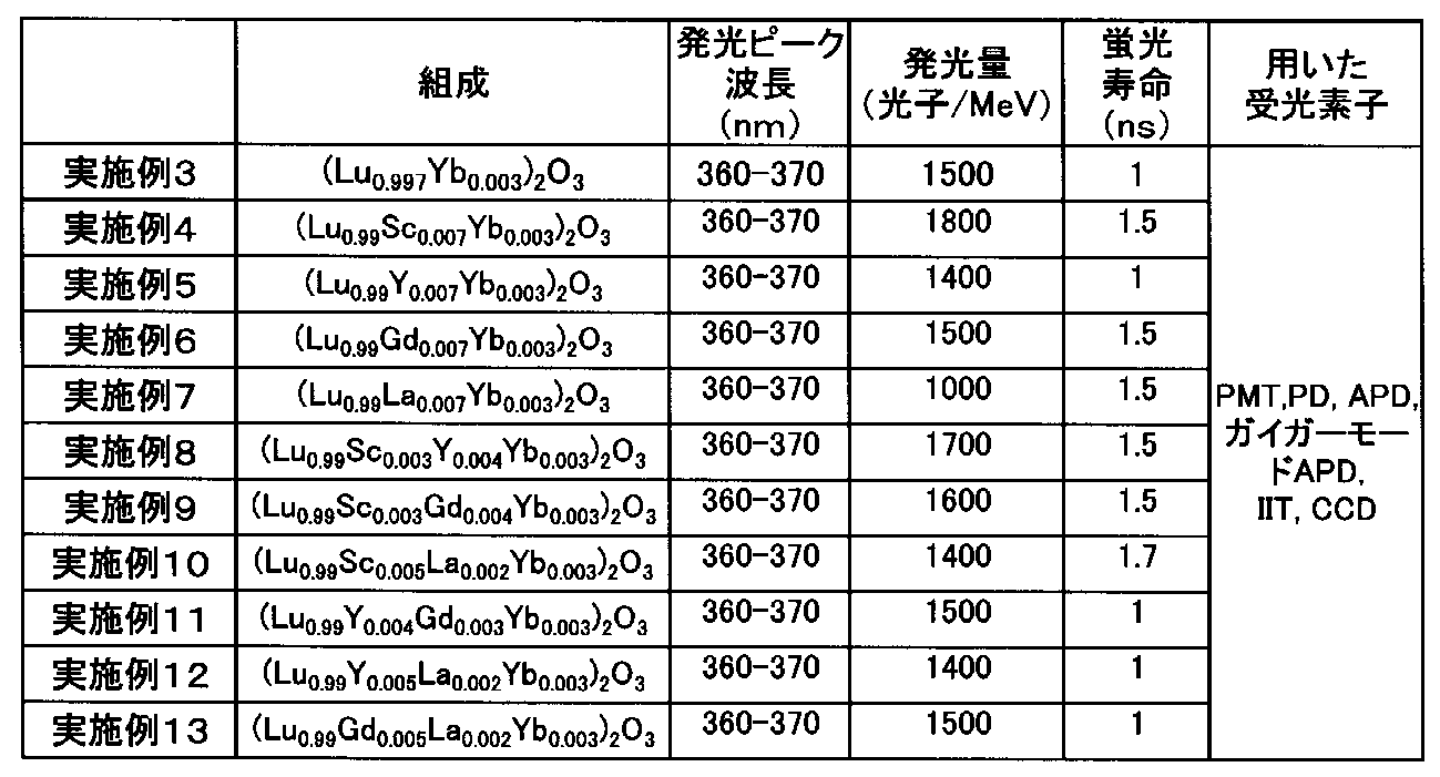
実施例14として、配合比を(Gd0.997Yb0.003)2O3とした蛍光材料を作製した。
このシンチレータ13用単結晶の作製にはマイクロ引下げ法を用いた。融液としては、単結晶が(Gd0.997Yb0.003)2O3の組成比となるようにGd2O3及びYb2O3の酸化物粉末を混合したものを用いた。つまり、純度99.99%の酸化物粉末原料を調合し、Re金属を坩堝として用いた。雰囲気としては、Ar(97%)ガス及びH2(3%)ガスからなる混合ガスを用いた。作製する単結晶と同じ組成の単結晶を[111]方位で方位切断して種結晶とした。固体と液体の界面をCCDカメラで観察し、適切な温度と結晶作製速度を決定した。結晶作製速度は0.05~0.1mm/分が典型的な条件であった。
このシンチレータ13用単結晶の作製にはマイクロ引下げ法を用いた。融液としては、単結晶が(Gd0.997Yb0.003)2O3の組成比となるようにGd2O3及びYb2O3の酸化物粉末を混合したものを用いた。つまり、純度99.99%の酸化物粉末原料を調合し、Re金属を坩堝として用いた。雰囲気としては、Ar(97%)ガス及びH2(3%)ガスからなる混合ガスを用いた。作製する単結晶と同じ組成の単結晶を[111]方位で方位切断して種結晶とした。固体と液体の界面をCCDカメラで観察し、適切な温度と結晶作製速度を決定した。結晶作製速度は0.05~0.1mm/分が典型的な条件であった。
(Gd0.997Yb0.003)2O3からなるシンチレータ13を用いた放射線検出器10を製作し、放射線検査装置20に組み込み、実施例3と同様にシンチレータ13の特性を測定した。実施例14のシンチレータ13では、受光ピーク波長は360~370nmであり、発光量は1600光子/MeV、蛍光寿命は1ns程度であった。実施例14のシンチレータ13では、実施例3のLuがGdに置換されているが、受光ピーク波長は実施例3と同様に360~370nmである。さらに、実施例14の発光量及び蛍光寿命も実施例3と同様であった。
実施例15として、配合比を(Gd0.947Sc0.05Yb0.003)2O3とした蛍光材料を作製した。
実施例15では、実施例14と同様に(Gd0.947Sc0.05Yb0.003)2O3からなるシンチレータ13を用いた放射線検出器10を製作し、放射線検査装置20に組み込み、実施例3と同様にシンチレータ13の特性を測定した。実施例15のシンチレータ13では、受光ピーク波長は360~370nmであり、発光量は1800光子/MeV、蛍光寿命は1.5ns程度であった。
実施例15では、実施例14と同様に(Gd0.947Sc0.05Yb0.003)2O3からなるシンチレータ13を用いた放射線検出器10を製作し、放射線検査装置20に組み込み、実施例3と同様にシンチレータ13の特性を測定した。実施例15のシンチレータ13では、受光ピーク波長は360~370nmであり、発光量は1800光子/MeV、蛍光寿命は1.5ns程度であった。
実施例16として、配合比を(Gd0.947Y0.05Yb0.003)2O3とした蛍光材料を作製した。
実施例16では、実施例14と同様に(Gd0.947Y0.05Yb0.003)2O3からなるシンチレータ13を用いた放射線検出器10を製作し、放射線検査装置20に組み込み、実施例3と同様にシンチレータ13の特性を測定した。実施例16のシンチレータ13では、受光ピーク波長は360~370nmであり、発光量は1600光子/MeV、蛍光寿命は1ns程度であった。
実施例16では、実施例14と同様に(Gd0.947Y0.05Yb0.003)2O3からなるシンチレータ13を用いた放射線検出器10を製作し、放射線検査装置20に組み込み、実施例3と同様にシンチレータ13の特性を測定した。実施例16のシンチレータ13では、受光ピーク波長は360~370nmであり、発光量は1600光子/MeV、蛍光寿命は1ns程度であった。
実施例17として、配合比を(Gd0.947La0.05Yb0.003)2O3とした蛍光材料を作製した。
実施例17では、実施例14と同様に(Gd0.947La0.05Yb0.003)2O3からなるシンチレータ13を用いた放射線検出器10を製作し、放射線検査装置20に組み込み、実施例3と同様にシンチレータ13の特性を測定した。実施例17のシンチレータ13では、受光ピーク波長は360~370nmであり、発光量は1200光子/MeV、蛍光寿命は1ns程度であった。実施例14~17のシンチレータ13を用いた放射線検出器10にγ線を照射したときの発光ピーク波長、発光量及び蛍光寿命を表3に纏めて示す。
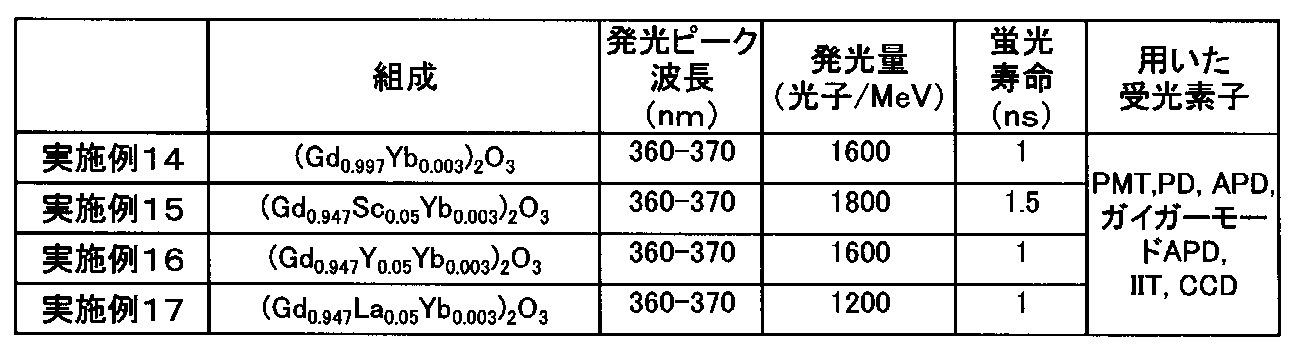
実施例17では、実施例14と同様に(Gd0.947La0.05Yb0.003)2O3からなるシンチレータ13を用いた放射線検出器10を製作し、放射線検査装置20に組み込み、実施例3と同様にシンチレータ13の特性を測定した。実施例17のシンチレータ13では、受光ピーク波長は360~370nmであり、発光量は1200光子/MeV、蛍光寿命は1ns程度であった。実施例14~17のシンチレータ13を用いた放射線検出器10にγ線を照射したときの発光ピーク波長、発光量及び蛍光寿命を表3に纏めて示す。
実施例18として、配合比を(La0.997Yb0.003)2O3とした蛍光材料を作製した。
実施例18~21では、実施例1と同様に多結晶を用いた。実施例18では、(La0.997Yb0.003)2O3からなるシンチレータ13を用いた放射線検出器10を製作し、放射線検査装置20に組み込み、実施例3と同様にシンチレータ13の特性を測定した。実施例18のシンチレータ13では、受光ピーク波長は360~370nmであり、発光量は200光子/MeV、蛍光寿命は1ns程度であった。実施例14のシンチレータ13では、実施例3のLuがLaに置換されているが、受光ピーク波長は実施例3と同様に360~370nmである。さらに、実施例14の発光量は、実施例3の13%程度となったが、蛍光寿命は実施例3と同様であった。
実施例18~21では、実施例1と同様に多結晶を用いた。実施例18では、(La0.997Yb0.003)2O3からなるシンチレータ13を用いた放射線検出器10を製作し、放射線検査装置20に組み込み、実施例3と同様にシンチレータ13の特性を測定した。実施例18のシンチレータ13では、受光ピーク波長は360~370nmであり、発光量は200光子/MeV、蛍光寿命は1ns程度であった。実施例14のシンチレータ13では、実施例3のLuがLaに置換されているが、受光ピーク波長は実施例3と同様に360~370nmである。さらに、実施例14の発光量は、実施例3の13%程度となったが、蛍光寿命は実施例3と同様であった。
実施例19として、配合比を(La0.947Sc0.05Yb0.003)2O3とした蛍光材料を作製した。
実施例19では、(La0.947Sc0.05Yb0.003)2O3からなるシンチレータ13を用いた放射線検出器10を製作し、放射線検査装置20に組み込み、実施例3と同様にシンチレータ13の特性を測定した。実施例19のシンチレータ13では、受光ピーク波長は360~370nmであり、発光量は400光子/MeV、蛍光寿命は1.5ns程度であった。
実施例19では、(La0.947Sc0.05Yb0.003)2O3からなるシンチレータ13を用いた放射線検出器10を製作し、放射線検査装置20に組み込み、実施例3と同様にシンチレータ13の特性を測定した。実施例19のシンチレータ13では、受光ピーク波長は360~370nmであり、発光量は400光子/MeV、蛍光寿命は1.5ns程度であった。
実施例20として、配合比を(La0.947Y0.05Yb0.003)2O3とした蛍光材料を作製した。
実施例20では、(La0.947Y0.05Yb0.003)2O3からなるシンチレータ13を用いた放射線検出器10を製作し、放射線検査装置20に組み込み、実施例3と同様にシンチレータ13の特性を測定した。実施例20のシンチレータ13では、受光ピーク波長は360~370nmであり、発光量は300光子/MeV、蛍光寿命は1ns程度であった。
実施例20では、(La0.947Y0.05Yb0.003)2O3からなるシンチレータ13を用いた放射線検出器10を製作し、放射線検査装置20に組み込み、実施例3と同様にシンチレータ13の特性を測定した。実施例20のシンチレータ13では、受光ピーク波長は360~370nmであり、発光量は300光子/MeV、蛍光寿命は1ns程度であった。
実施例21として、配合比を(La0.947Gd0.05Yb0.003)2O3とした蛍光材料を作製した。
実施例21では、(La0.947Gd0.05Yb0.003)2O3からなるシンチレータ13を用いた放射線検出器10を製作し、放射線検査装置20に組み込み、実施例3と同様にシンチレータ13の特性を測定した。実施例21のシンチレータ13では、受光ピーク波長は360~370nmであり、発光量は300光子/MeV、蛍光寿命は1ns程度であった。実施例18~21のシンチレータ13を用いた放射線検出器10にγ線を照射したときの発光ピーク波長、発光量及び蛍光寿命を表4に纏めて示す。
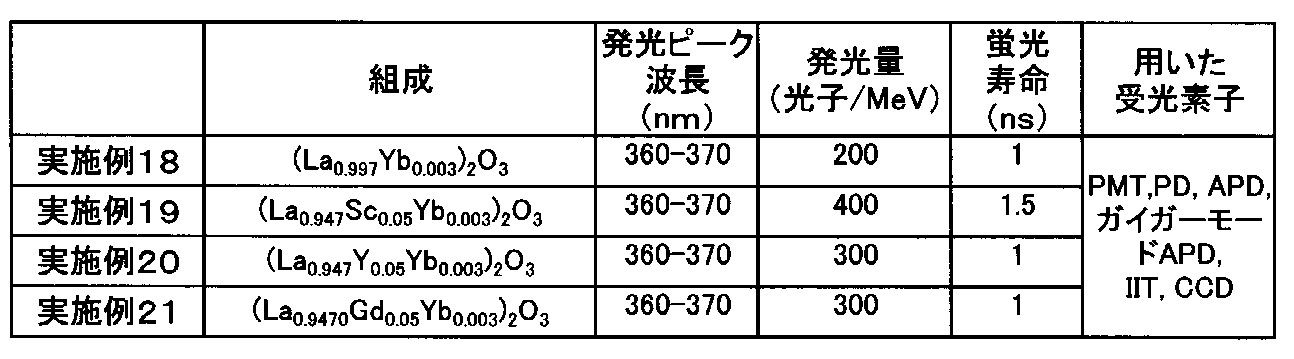
実施例21では、(La0.947Gd0.05Yb0.003)2O3からなるシンチレータ13を用いた放射線検出器10を製作し、放射線検査装置20に組み込み、実施例3と同様にシンチレータ13の特性を測定した。実施例21のシンチレータ13では、受光ピーク波長は360~370nmであり、発光量は300光子/MeV、蛍光寿命は1ns程度であった。実施例18~21のシンチレータ13を用いた放射線検出器10にγ線を照射したときの発光ピーク波長、発光量及び蛍光寿命を表4に纏めて示す。
実施例22として、配合比を(Sc0.997Yb0.003)2O3とした蛍光材料を作製した。
最初に、酸化スカンジウム原料粉末を作製した(特許文献2、段落[0040]参照)。純度99.9%以上Si5ppmの酸化スカンジウムを塩酸に溶解させ、濃度0.25M(mol・dm-3)の塩化スカンジウム水溶液を調製した。この溶液500mlをポリテトラフルオロエチレン製ビーカーに入れ攪拌した。塩化スカンジウム水溶液に、濃度0.5M(mol・dm-3)の炭酸水素アンモニウム溶液を5ml/minの速さでpH8.0となるまで滴下し、攪拌を続けながら室温で10日間養生を行った。養生後、濾過及び超純水を用いた水洗を数回繰り返した後、150℃の乾燥機に入れ2日間乾燥した。得られた前駆体粉末をアルミナ製坩堝に入れ、電気炉で仮焼(1250℃×3時間)することにより、平均一次粒子径0.35μmの酸化スカンジウム原料粉末を作製した。
最初に、酸化スカンジウム原料粉末を作製した(特許文献2、段落[0040]参照)。純度99.9%以上Si5ppmの酸化スカンジウムを塩酸に溶解させ、濃度0.25M(mol・dm-3)の塩化スカンジウム水溶液を調製した。この溶液500mlをポリテトラフルオロエチレン製ビーカーに入れ攪拌した。塩化スカンジウム水溶液に、濃度0.5M(mol・dm-3)の炭酸水素アンモニウム溶液を5ml/minの速さでpH8.0となるまで滴下し、攪拌を続けながら室温で10日間養生を行った。養生後、濾過及び超純水を用いた水洗を数回繰り返した後、150℃の乾燥機に入れ2日間乾燥した。得られた前駆体粉末をアルミナ製坩堝に入れ、電気炉で仮焼(1250℃×3時間)することにより、平均一次粒子径0.35μmの酸化スカンジウム原料粉末を作製した。
次に、酸化スカンジウム原料粉末と酸化イッテルビウム原料粉末(信越化学工業(株)製、純度99.99%、BET比表面積値2.7m2/g)とを、(Sc0.997Yb0.003)2O3の組成比となるように秤量した後、混合して原料混合粉末とした。この原料混合粉末を、実施例1と同様に処理して、1700℃で5時間真空焼成を行うことによって、実施例22の(Sc0.997Yb0.003)2O3からなるシンチレータ13を作製した。次に、このシンチレータ13を用いた放射線検出器10を製作した。放射線検出器10を放射線検査装置20に組み込み、実施例3と同様にシンチレータ13の特性を測定した。
実施例22のシンチレータ13では、受光ピーク波長は360~370nmであり、発光量は2000光子/MeV、蛍光寿命は2ns程度であった。実施例22のシンチレータ13では、実施例3のLuがScに置換されているが、受光ピーク波長は実施例3と同様に360~370nmである。さらに、実施例22の発光量は、実施例3の133%程度となったが、蛍光寿命は実施例3の2倍程度の2nsであった。
実施例23として、配合比を(Sc0.99Y0.007Yb0.003)2O3とした蛍光材料を作製した。
実施例22で作製した酸化スカンジウム原料粉末と酸化イットリウム原料粉末(信越化学工業(株)製、純度99.99%、BET比表面積値4.5m2/g)と酸化イッテルビウム(信越化学工業(株)製、純度99.99%、BET比表面積値2.7m2/g)とを、(Sc0.99Y0.007Yb0.003)2O3の組成比となるように秤量した後、混合して原料混合粉末とした。この原料混合粉末を実施例1と同様に処理して、1700℃で5時間真空焼成を行うことによって、実施例23の(Sc0.99Y0.007Yb0.003)2O3からなるシンチレータ13を作製した。次に、このシンチレータ13を用いた放射線検出器10を製作した。放射線検出器10を放射線検査装置20に組み込み、実施例3と同様にシンチレータ13の特性を測定した。
実施例22で作製した酸化スカンジウム原料粉末と酸化イットリウム原料粉末(信越化学工業(株)製、純度99.99%、BET比表面積値4.5m2/g)と酸化イッテルビウム(信越化学工業(株)製、純度99.99%、BET比表面積値2.7m2/g)とを、(Sc0.99Y0.007Yb0.003)2O3の組成比となるように秤量した後、混合して原料混合粉末とした。この原料混合粉末を実施例1と同様に処理して、1700℃で5時間真空焼成を行うことによって、実施例23の(Sc0.99Y0.007Yb0.003)2O3からなるシンチレータ13を作製した。次に、このシンチレータ13を用いた放射線検出器10を製作した。放射線検出器10を放射線検査装置20に組み込み、実施例3と同様にシンチレータ13の特性を測定した。
実施例23のシンチレータ13では、受光ピーク波長は360~370nmであり、発光量は1800光子/MeV、蛍光寿命は1.8ns程度であった。
実施例24として、配合比を(Sc0.99Gd0.007Yb0.003)2O3とした蛍光材料を作製した。
実施例22で作製した酸化スカンジウム原料粉末と酸化イットリウム原料粉末(信越化学工業(株)製、純度99.99%、BET比表面積値4.5m2/g)と酸化イッテルビウム原料粉末(信越化学工業(株)製、純度99.99%、BET比表面積値2.7m2/g)とを、(Sc0.99Gd0.007Yb0.003)2O3の組成比となるように秤量した後、混合して原料混合粉末とした。この原料混合粉末を実施例1と同様に処理して、1700℃で5時間真空焼成を行うことによって、実施例24の(Sc0.99Gd0.007Yb0.003)2O3からなるシンチレータ13を作製した。次に、このシンチレータ13を用いた放射線検出器10を製作した。放射線検出器10を放射線検査装置20に組み込み、実施例3と同様にシンチレータ13の特性を測定した。
実施例22で作製した酸化スカンジウム原料粉末と酸化イットリウム原料粉末(信越化学工業(株)製、純度99.99%、BET比表面積値4.5m2/g)と酸化イッテルビウム原料粉末(信越化学工業(株)製、純度99.99%、BET比表面積値2.7m2/g)とを、(Sc0.99Gd0.007Yb0.003)2O3の組成比となるように秤量した後、混合して原料混合粉末とした。この原料混合粉末を実施例1と同様に処理して、1700℃で5時間真空焼成を行うことによって、実施例24の(Sc0.99Gd0.007Yb0.003)2O3からなるシンチレータ13を作製した。次に、このシンチレータ13を用いた放射線検出器10を製作した。放射線検出器10を放射線検査装置20に組み込み、実施例3と同様にシンチレータ13の特性を測定した。
実施例24のシンチレータ13では、受光ピーク波長は360~370nmであり、発光量は1800光子/MeV、蛍光寿命は2ns程度であった。
実施例25として、配合比を(Sc0.99Gd0.007Yb0.003)2O3とした蛍光材料を作製した。
実施例22で作製した酸化スカンジウム原料粉末と酸化イットリウム原料粉末(信越化学工業(株)製、純度99.99%、BET比表面積値4.5m2/g)と酸化イッテルビウム原料粉末(信越化学工業(株)製、純度99.99%、BET比表面積値2.7m2/g)とを、(Sc0.99Gd0.007Yb0.003)2O3の組成比となるように秤量した後、混合して原料混合粉末とした。この原料混合粉末を実施例1と同様に処理して、1700℃で5時間真空焼成を行うことによって、実施例25の(Sc0.99Gd0.007Yb0.003)2O3からなるシンチレータ13を作製した。次に、このシンチレータ13を用いた放射線検出器10を製作した。放射線検出器10を放射線検査装置20に組み込み、実施例3と同様にシンチレータ13の特性を測定した。
実施例22で作製した酸化スカンジウム原料粉末と酸化イットリウム原料粉末(信越化学工業(株)製、純度99.99%、BET比表面積値4.5m2/g)と酸化イッテルビウム原料粉末(信越化学工業(株)製、純度99.99%、BET比表面積値2.7m2/g)とを、(Sc0.99Gd0.007Yb0.003)2O3の組成比となるように秤量した後、混合して原料混合粉末とした。この原料混合粉末を実施例1と同様に処理して、1700℃で5時間真空焼成を行うことによって、実施例25の(Sc0.99Gd0.007Yb0.003)2O3からなるシンチレータ13を作製した。次に、このシンチレータ13を用いた放射線検出器10を製作した。放射線検出器10を放射線検査装置20に組み込み、実施例3と同様にシンチレータ13の特性を測定した。
実施例25のシンチレータ13では、受光ピーク波長は360~370nmであり、発光量は1600光子/MeV、蛍光寿命は2ns程度であった。
実施例22~25のシンチレータ13を用いた放射線検出器10にγ線を照射したときの発光ピーク波長、発光量及び蛍光寿命を表5に纏めて示す。
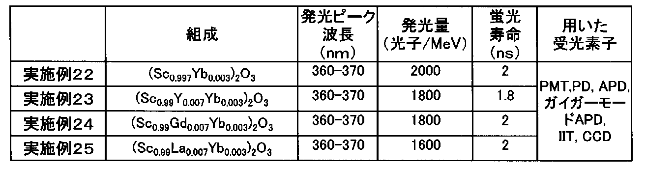
実施例26として、配合比を(Y0.997Yb0.003)2O3とした蛍光材料を作製した。
最初に、酸化イットリウム原料粉末を作製した、特許文献3の段落[0037]に記載されているように、特開平11-157933号公報の手法に基づき、平均一次粒子径0.3μm、純度99.9%以上、Si3wtppmの酸化イットリウム原料粉末を作製した。
即ち、イットリウムの硝酸塩水溶液と尿素の水溶液と硫酸アンモニウムの水溶液とを混合して、イットリウム:尿素:硫酸アンモニウムがモル比で1:6:1とし、オートクレーブ中125℃で2時間水熱反応させ、イットリウムの炭酸塩を得た。得られた炭酸塩を純水で洗浄し、乾燥した。次に、この乾燥粉末を、アルミナ坩堝を用い大気雰囲気中1200℃で3時間仮焼して、酸化イットリウム原料粉末とした。
上記の酸化イットリウム原料粉末と酸化イッテルビウム原料粉末(信越化学工業(株)製、純度99.99%、BET比表面積値2.7m2/g)とを、(Y0.997Yb0.003)2O3の組成比となるように秤量した後、混合して原料混合粉末とした。この原料混合粉末を実施例1と同様に処理して、1600℃で10時間真空焼成を行うことによって、実施例26の(Y0.997Yb0.003)2O3からなるシンチレータ13を作製した。次に、このシンチレータ13を用いた放射線検出器10を製作した。放射線検出器10を放射線検査装置20に組み込み、実施例3と同様にシンチレータ13の特性を測定した。
実施例26のシンチレータ13では、受光ピーク波長は360~370nmであり、発光量は200光子/MeV、蛍光寿命は1ns程度であった。実施例22のシンチレータ13では、実施例3のLuがYに置換されているが、受光ピーク波長は実施例3と同様に360~370nmである。さらに、実施例22の発光量は、実施例3の13%程度となったが、蛍光寿命は実施例3と同じ1nsであった。
実施例27として、配合比を(Y0.99Sc0.007Yb0.003)2O3とした蛍光材料を作製した。
実施例26で作製した酸化イットリウム原料粉末と酸化スカンジウム原料粉末(信越化学工業(株)製、純度99.99%、BET比表面積値3.5m2/g)と、酸化イッテルビウム(信越化学工業(株)製、純度99.99%、BET比表面積値2.7m2/g)とを、(Y0.99Sc0.007Yb0.003)2O3の組成比となるように秤量した後、混合して原料混合粉末とした。この原料混合粉末を実施例1と同様に処理して、1600℃で10時間真空焼成を行うことによって、実施例27の(Y0.99Sc0.007Yb0.003)2O3からなるシンチレータ13を作製した。次に、このシンチレータ13を用いた放射線検出器10を製作した。放射線検出器10を放射線検査装置20に組み込み、実施例3と同様にシンチレータ13の特性を測定した。
実施例26で作製した酸化イットリウム原料粉末と酸化スカンジウム原料粉末(信越化学工業(株)製、純度99.99%、BET比表面積値3.5m2/g)と、酸化イッテルビウム(信越化学工業(株)製、純度99.99%、BET比表面積値2.7m2/g)とを、(Y0.99Sc0.007Yb0.003)2O3の組成比となるように秤量した後、混合して原料混合粉末とした。この原料混合粉末を実施例1と同様に処理して、1600℃で10時間真空焼成を行うことによって、実施例27の(Y0.99Sc0.007Yb0.003)2O3からなるシンチレータ13を作製した。次に、このシンチレータ13を用いた放射線検出器10を製作した。放射線検出器10を放射線検査装置20に組み込み、実施例3と同様にシンチレータ13の特性を測定した。
実施例27のシンチレータ13では、受光ピーク波長は360~370nmであり、発光量は250光子/MeV、蛍光寿命は2ns程度であった。
実施例28として、配合比を(Y0.99Gd0.007Yb0.003)2O3とした蛍光材料を作製した。
実施例26で作製した酸化イットリウム原料粉末と酸化ガドリニウム原料粉末(信越化学工業(株)製、純度99.99%、BET比表面積値4.3m2/g)と酸化イッテルビウム原料粉末(信越化学工業(株)製、純度99.99%、BET比表面積値2.7m2/g)とを、(Y0.99Gd0.007Yb0.003)2O3の組成比となるように秤量した後、混合して原料混合粉末とした。この原料混合粉末を実施例1と同様に処理して、1600℃で10時間真空焼成を行うことによって、実施例28の(Y0.99Gd0.007Yb0.003)2O3からなるシンチレータ13を作製した。次に、このシンチレータ13を用いた放射線検出器10を製作した。放射線検出器10を放射線検査装置20に組み込み、実施例3と同様にシンチレータ13の特性を測定した。
実施例26で作製した酸化イットリウム原料粉末と酸化ガドリニウム原料粉末(信越化学工業(株)製、純度99.99%、BET比表面積値4.3m2/g)と酸化イッテルビウム原料粉末(信越化学工業(株)製、純度99.99%、BET比表面積値2.7m2/g)とを、(Y0.99Gd0.007Yb0.003)2O3の組成比となるように秤量した後、混合して原料混合粉末とした。この原料混合粉末を実施例1と同様に処理して、1600℃で10時間真空焼成を行うことによって、実施例28の(Y0.99Gd0.007Yb0.003)2O3からなるシンチレータ13を作製した。次に、このシンチレータ13を用いた放射線検出器10を製作した。放射線検出器10を放射線検査装置20に組み込み、実施例3と同様にシンチレータ13の特性を測定した。
実施例28のシンチレータ13では、受光ピーク波長は360~370nmであり、発光量は300光子/MeV、蛍光寿命は1.5ns程度であった。
実施例29として、配合比を(Y0.995La0.002Yb0.003)2O3とした蛍光材料を作製した。
実施例26で作製した酸化イットリウム原料粉末と酸化ランタン原料粉末(信越化学工業(株)製、純度99.99%、BET比表面積値3.8m2/g)と酸化イッテルビウム原料粉末(信越化学工業(株)製、純度99.99%、BET比表面積値2.7m2/g)とを、(Y0.995La0.002Yb0.003)2O3の組成比となるように秤量した後、混合して原料混合粉末とした。この原料混合粉末を実施例1と同様に処理して、1600℃で10時間真空焼成を行うことによって、実施例29の(Y0.995La0.002Yb0.003)2O3からなるシンチレータ13を作製した。次に、このシンチレータ13を用いた放射線検出器10を製作した。放射線検出器10を放射線検査装置20に組み込み、実施例3と同様にシンチレータ13の特性を測定した。
実施例26で作製した酸化イットリウム原料粉末と酸化ランタン原料粉末(信越化学工業(株)製、純度99.99%、BET比表面積値3.8m2/g)と酸化イッテルビウム原料粉末(信越化学工業(株)製、純度99.99%、BET比表面積値2.7m2/g)とを、(Y0.995La0.002Yb0.003)2O3の組成比となるように秤量した後、混合して原料混合粉末とした。この原料混合粉末を実施例1と同様に処理して、1600℃で10時間真空焼成を行うことによって、実施例29の(Y0.995La0.002Yb0.003)2O3からなるシンチレータ13を作製した。次に、このシンチレータ13を用いた放射線検出器10を製作した。放射線検出器10を放射線検査装置20に組み込み、実施例3と同様にシンチレータ13の特性を測定した。
実施例29のシンチレータ13では、受光ピーク波長は360~370nmであり、発光量は250光子/MeV、蛍光寿命は1.5ns程度であった。
実施例30として、配合比を(Y0.99Sc0.004Gd0.003Yb0.003)2O3とした蛍光材料を作製した。
実施例26で作製した酸化イットリウム原料粉末と酸化スカンジウム原料粉末(信越化学工業(株)製、純度99.99%、BET比表面積値3.5m2/g)と酸化ガドリニウム原料粉末(信越化学工業(株)製、純度99.99%、BET比表面積値4.3m2/g)と酸化イッテルビウム原料粉末(信越化学工業(株)製、純度99.99%、BET比表面積値2.7m2/g)とを、(Y0.99Sc0.004Gd0.003Yb0.003)2O3の組成比となるように秤量した後、混合して原料混合粉末とした。この原料混合粉末を実施例1と同様に処理して、1600℃で10時間真空焼成を行うことによって、実施例30の(Y0.99Sc0.004Gd0.003Yb0.003)2O3からなるシンチレータ13を作製した。次に、このシンチレータ13を用いた放射線検出器10を製作した。放射線検出器10を放射線検査装置20に組み込み、実施例3と同様にシンチレータ13の特性を測定した。
実施例26で作製した酸化イットリウム原料粉末と酸化スカンジウム原料粉末(信越化学工業(株)製、純度99.99%、BET比表面積値3.5m2/g)と酸化ガドリニウム原料粉末(信越化学工業(株)製、純度99.99%、BET比表面積値4.3m2/g)と酸化イッテルビウム原料粉末(信越化学工業(株)製、純度99.99%、BET比表面積値2.7m2/g)とを、(Y0.99Sc0.004Gd0.003Yb0.003)2O3の組成比となるように秤量した後、混合して原料混合粉末とした。この原料混合粉末を実施例1と同様に処理して、1600℃で10時間真空焼成を行うことによって、実施例30の(Y0.99Sc0.004Gd0.003Yb0.003)2O3からなるシンチレータ13を作製した。次に、このシンチレータ13を用いた放射線検出器10を製作した。放射線検出器10を放射線検査装置20に組み込み、実施例3と同様にシンチレータ13の特性を測定した。
実施例30のシンチレータ13では、受光ピーク波長は360~370nmであり、発光量は500光子/MeV、蛍光寿命は1.5ns程度であった。
実施例31として、配合比を(Y0.99Sc0.005La0.002Yb0.003)2O3とした蛍光材料を作製した。
実施例26で作製した酸化イットリウム原料粉末と酸化スカンジウム原料粉末(信越化学工業(株)製、純度99.99%、BET比表面積値3.5m2/g)と酸化ランタン原料粉末(信越化学工業(株)製、純度99.99%、BET比表面積値3.8m2/g)と酸化イッテルビウム原料粉末(信越化学工業(株)製、純度99.99%、BET比表面積値2.7m2/g)とを、(Y0.99Sc0.005La0.002Yb0.003)2O3の組成比となるように秤量した後、混合して原料混合粉末とした。この原料混合粉末を実施例1と同様に処理して、1600℃で10時間真空焼成を行うことによって実施例31の(Y0.99Sc0.005La0.002Yb0.003)2O3からなるシンチレータ13を作製した。次に、このシンチレータ13を用いた放射線検出器10を製作した。放射線検出器10を放射線検査装置20に組み込み、実施例3と同様にシンチレータ13の特性を測定した。
実施例26で作製した酸化イットリウム原料粉末と酸化スカンジウム原料粉末(信越化学工業(株)製、純度99.99%、BET比表面積値3.5m2/g)と酸化ランタン原料粉末(信越化学工業(株)製、純度99.99%、BET比表面積値3.8m2/g)と酸化イッテルビウム原料粉末(信越化学工業(株)製、純度99.99%、BET比表面積値2.7m2/g)とを、(Y0.99Sc0.005La0.002Yb0.003)2O3の組成比となるように秤量した後、混合して原料混合粉末とした。この原料混合粉末を実施例1と同様に処理して、1600℃で10時間真空焼成を行うことによって実施例31の(Y0.99Sc0.005La0.002Yb0.003)2O3からなるシンチレータ13を作製した。次に、このシンチレータ13を用いた放射線検出器10を製作した。放射線検出器10を放射線検査装置20に組み込み、実施例3と同様にシンチレータ13の特性を測定した。
実施例31のシンチレータ13では、受光ピーク波長は360~370nmであり、発光量は600光子/MeV、蛍光寿命は1.5ns程度であった。
実施例32として、配合比を(Y0.99Gd0.005La0.002Yb0.003)2O3とした蛍光材料を作製した。
実施例26で作製した酸化イットリウム原料粉末と酸化スカンジウム原料粉末(信越化学工業(株)製、純度99.99%、BET比表面積値3.5m2/g)と酸化ランタン原料粉末(信越化学工業(株)製、純度99.99%、BET比表面積値3.8m2/g)と酸化イッテルビウム原料粉末(信越化学工業(株)製、純度99.99%、BET比表面積値2.7m2/g)とを、(Y0.99Gd0.005La0.002Yb0.003)2O3の組成比となるように秤量した後、混合して原料混合粉末とした。この原料混合粉末を実施例1と同様に処理して、1600℃で10時間真空焼成を行うことによって実施例32の(Y0.99Gd0.005La0.002Yb0.003)2O3からなるシンチレータ13を作製した。次に、このシンチレータ13を用いた放射線検出器10を製作した。放射線検出器10を放射線検査装置20に組み込み、実施例3と同様にシンチレータ13の特性を測定した。
実施例26で作製した酸化イットリウム原料粉末と酸化スカンジウム原料粉末(信越化学工業(株)製、純度99.99%、BET比表面積値3.5m2/g)と酸化ランタン原料粉末(信越化学工業(株)製、純度99.99%、BET比表面積値3.8m2/g)と酸化イッテルビウム原料粉末(信越化学工業(株)製、純度99.99%、BET比表面積値2.7m2/g)とを、(Y0.99Gd0.005La0.002Yb0.003)2O3の組成比となるように秤量した後、混合して原料混合粉末とした。この原料混合粉末を実施例1と同様に処理して、1600℃で10時間真空焼成を行うことによって実施例32の(Y0.99Gd0.005La0.002Yb0.003)2O3からなるシンチレータ13を作製した。次に、このシンチレータ13を用いた放射線検出器10を製作した。放射線検出器10を放射線検査装置20に組み込み、実施例3と同様にシンチレータ13の特性を測定した。
実施例32のシンチレータ13では、受光ピーク波長は360~370nmであり、発光量は500光子/MeV、蛍光寿命は1ns程度であった。
実施例26~32のシンチレータ13を用いた放射線検出器10にγ線を照射したときの発光ピーク波長、発光量及び蛍光寿命を表6に纏めて示す。
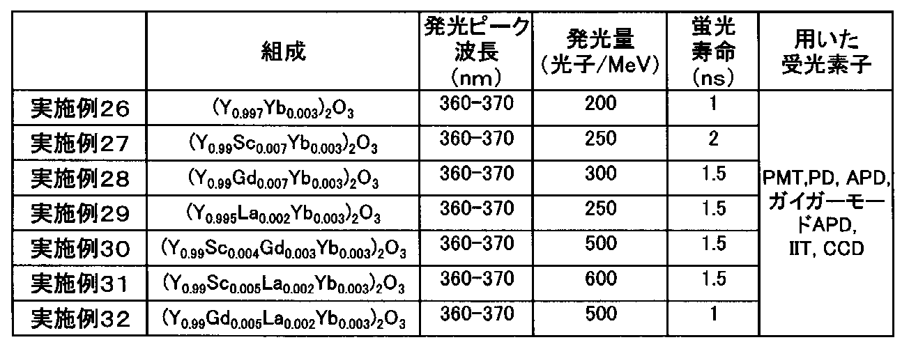
本発明は、上記実施の形態に限定されるものではなく、特許請求の範囲に記載した発明の範囲内で種々の変形が可能であり、それらも本発明の範囲内に含まれることはいうまでもない。例えば、シンチレータ13の組成は、蛍光発光量や蛍光寿命を考慮して適宜に設定すればよい。
Claims (15)
- 化学式(R1-XYbX)2O3(ここで、Rは、Sc、Y及びランタノイドで構成される希土類元素から選択される1つ以上の元素であり、0<x<0.1)で表されることを特徴とする、シンチレータ用発光材料。
- 前記希土類元素は、Sc、Y、La、Gd及びLuから選択される1つ以上の元素であることを特徴とする、請求項1に記載のシンチレータ用発光材料。
- 前記シンチレータ用発光材料は、放射線の照射によって大凡300~600nmの波長領域に発光ピーク波長を有している蛍光を発生することを特徴とする、請求項1又は2に記載のシンチレータ用発光材料。
- 前記シンチレータ用発光材料は、前記発光ピーク波長に対応する300~530nmの波長領域における吸収が少なく、透明であることを特徴とする、請求項3に記載のシンチレータ用発光材料。
- 前記シンチレータ用発光材料は、Yb3+の電荷移動状態(CTS)からの遷移に起因する蛍光を発光することを特徴とする、請求項1に記載のシンチレータ用発光材料。
- 前記シンチレータ用発光材料は、多結晶又は結晶からなることを特徴とする、請求項1~5の何れかに記載のシンチレータ用発光材料。
- 請求項1~6の何れかに記載のシンチレータ用発光材料から構成したことを特徴とする、シンチレータ。
- 室温における蛍光寿命は、5ns以下であることを特徴とする、請求項7に記載のシンチレータ。
- 請求項1~6の何れかに記載のシンチレータ用発光材料から構成したシンチレータと該シンチレータからの蛍光を受光する受光素子とを備えたことを特徴とする、放射線検出器。
- 前記受光素子は、光電子増倍管、フォトダイオード、アバランシェフォトダイオード、ガイガーモードアバランシェフォトダイオード、イメージインテンシファイア、電荷結合素子の何れかであることを特徴とする、請求項9に記載の放射線検出器。
- 請求項9又は10に記載の放射線検出器を備えることを特徴とする、放射線検査装置。
- 請求項1~6の何れかに記載のシンチレータ用発光材料の製造方法であって、
前記Rの酸化物粉末と前記Ybの酸化物粉末とを混合して原料粉末の成形体とし、
上記成形体を所定の時間焼成することによって、(R1-XYbX)2O3の多結晶を製造することを特徴とする、シンチレータ用発光材料の製造方法。 - 前記酸化物粉末のBET比表面積が、2m2/g以上15m2/g以下で、5μmを超える2次凝集粒子が質量分率で10%以下であることを特徴とする、請求項12に記載のシンチレータ用発光材料の製造方法。
- 前記成形体の密度を58%以上とすることを特徴とする、請求項12に記載のシンチレータ用発光材料の製造方法。
- 請求項1~6の何れかに記載のシンチレータ用発光材料の製造方法であって、前記化学式(R1-XYbX)2O3(ここで、Rは、Sc、Y及びランタノイドで構成される希土類元素から選択される1つ以上の元素であり、0<x<0.1)で表される組成の原料粉末を用いて、シンチレータ用発光材料の単結晶を育成することを特徴とする、シンチレータ用発光材料の製造方法。
Applications Claiming Priority (2)
| Application Number | Priority Date | Filing Date | Title |
|---|---|---|---|
| JP2010291327A JP2012136667A (ja) | 2010-12-27 | 2010-12-27 | シンチレータ用発光材料、それを用いたシンチレータ及びそれを用いた放射線検出器並びに放射線検査装置 |
| JP2010-291327 | 2010-12-27 |
Publications (1)
| Publication Number | Publication Date |
|---|---|
| WO2012090936A1 true WO2012090936A1 (ja) | 2012-07-05 |
Family
ID=46383039
Family Applications (1)
| Application Number | Title | Priority Date | Filing Date |
|---|---|---|---|
| PCT/JP2011/080076 Ceased WO2012090936A1 (ja) | 2010-12-27 | 2011-12-26 | シンチレータ用発光材料、それを用いたシンチレータ及びそれを用いた放射線検出器並びに放射線検査装置 |
Country Status (2)
| Country | Link |
|---|---|
| JP (1) | JP2012136667A (ja) |
| WO (1) | WO2012090936A1 (ja) |
Cited By (1)
| Publication number | Priority date | Publication date | Assignee | Title |
|---|---|---|---|---|
| CN110622039A (zh) * | 2017-03-15 | 2019-12-27 | 德国史密斯海曼简化股份公司 | 用于检查系统的检测器和方法 |
Families Citing this family (3)
| Publication number | Priority date | Publication date | Assignee | Title |
|---|---|---|---|---|
| JP2015531414A (ja) * | 2012-09-11 | 2015-11-02 | オーシャンズ キング ライティング サイエンス アンド テクノロジー シーオー.,エルティーディー | ルテチウム酸化物発光材料、及び、その製造方法 |
| JP2019082409A (ja) * | 2017-10-31 | 2019-05-30 | 国立大学法人千葉大学 | Pet装置用シンチレーター及びこれを用いたpet装置 |
| WO2021132494A1 (ja) * | 2019-12-25 | 2021-07-01 | 三菱ケミカル株式会社 | シンチレータおよび放射線検出器 |
Citations (9)
| Publication number | Priority date | Publication date | Assignee | Title |
|---|---|---|---|---|
| JPS5930883A (ja) * | 1982-06-18 | 1984-02-18 | ゼネラル・エレクトリツク・カンパニイ | 希土類添加イツトリア−ガドリニアセラミツクシンチレ−タおよびその製法 |
| JPS5930882A (ja) * | 1982-06-18 | 1984-02-18 | ゼネラル・エレクトリツク・カンパニイ | 希土類添加イツトリア−ガドリニアセラミツクシンチレ−タおよびその製法 |
| JPS6438491A (en) * | 1982-06-18 | 1989-02-08 | Gen Electric | Rare earth metal element added yttria-gadonia ceramic scintillator |
| JPH06206769A (ja) * | 1992-07-28 | 1994-07-26 | Siemens Ag | 希土類−オキシスルフィドの高密度シンチレーションセラミックの製法及びレントゲンコンピューター断層撮影用セラミック体 |
| JP2000178547A (ja) * | 1998-12-16 | 2000-06-27 | Hitachi Metals Ltd | セラミックスシンチレータ |
| JP2003277191A (ja) * | 2002-03-26 | 2003-10-02 | Japan Science & Technology Corp | Yb混晶酸化物単結晶からなるシンチレータ用発光材料 |
| JP2005095514A (ja) * | 2003-09-26 | 2005-04-14 | Hitachi Medical Corp | 放射線検出器及びそれを用いたx線ct装置 |
| JP2010122166A (ja) * | 2008-11-21 | 2010-06-03 | Tohoku Univ | 放射線検出器および放射線検査装置 |
| JP2010169673A (ja) * | 2008-12-26 | 2010-08-05 | Tohoku Univ | 放射線検出器 |
-
2010
- 2010-12-27 JP JP2010291327A patent/JP2012136667A/ja active Pending
-
2011
- 2011-12-26 WO PCT/JP2011/080076 patent/WO2012090936A1/ja not_active Ceased
Patent Citations (9)
| Publication number | Priority date | Publication date | Assignee | Title |
|---|---|---|---|---|
| JPS5930883A (ja) * | 1982-06-18 | 1984-02-18 | ゼネラル・エレクトリツク・カンパニイ | 希土類添加イツトリア−ガドリニアセラミツクシンチレ−タおよびその製法 |
| JPS5930882A (ja) * | 1982-06-18 | 1984-02-18 | ゼネラル・エレクトリツク・カンパニイ | 希土類添加イツトリア−ガドリニアセラミツクシンチレ−タおよびその製法 |
| JPS6438491A (en) * | 1982-06-18 | 1989-02-08 | Gen Electric | Rare earth metal element added yttria-gadonia ceramic scintillator |
| JPH06206769A (ja) * | 1992-07-28 | 1994-07-26 | Siemens Ag | 希土類−オキシスルフィドの高密度シンチレーションセラミックの製法及びレントゲンコンピューター断層撮影用セラミック体 |
| JP2000178547A (ja) * | 1998-12-16 | 2000-06-27 | Hitachi Metals Ltd | セラミックスシンチレータ |
| JP2003277191A (ja) * | 2002-03-26 | 2003-10-02 | Japan Science & Technology Corp | Yb混晶酸化物単結晶からなるシンチレータ用発光材料 |
| JP2005095514A (ja) * | 2003-09-26 | 2005-04-14 | Hitachi Medical Corp | 放射線検出器及びそれを用いたx線ct装置 |
| JP2010122166A (ja) * | 2008-11-21 | 2010-06-03 | Tohoku Univ | 放射線検出器および放射線検査装置 |
| JP2010169673A (ja) * | 2008-12-26 | 2010-08-05 | Tohoku Univ | 放射線検出器 |
Cited By (2)
| Publication number | Priority date | Publication date | Assignee | Title |
|---|---|---|---|---|
| CN110622039A (zh) * | 2017-03-15 | 2019-12-27 | 德国史密斯海曼简化股份公司 | 用于检查系统的检测器和方法 |
| CN110622039B (zh) * | 2017-03-15 | 2023-10-24 | 德国史密斯海曼简化股份公司 | 用于检查系统的检测器和方法 |
Also Published As
| Publication number | Publication date |
|---|---|
| JP2012136667A (ja) | 2012-07-19 |
Similar Documents
| Publication | Publication Date | Title |
|---|---|---|
| JP5952746B2 (ja) | シンチレータ用ガーネット型単結晶、及びこれを用いた放射線検出器 | |
| JP5462515B2 (ja) | 透明セラミックス及びその製造方法並びにその透明セラミックスを用いたデバイス | |
| JP6644010B2 (ja) | 向上した耐放射線性を有する多重ドープルテチウム系オキシオルトシリケートシンチレータ | |
| US8431042B2 (en) | Solid state scintillator material, solid state scintillator, radiation detector, and radiation inspection apparatus | |
| CN1171973C (zh) | 磷光体和使用此磷光体的辐射探测器及使用此磷光体的x射线ct装置 | |
| US5116560A (en) | Method of forming rare earth oxide ceramic scintillator with ammonium dispersion of oxalate precipitates | |
| CA2059915C (en) | Method of forming yttria-gadolinia ceramic scintillator using hydroxide coprecipitation step | |
| US9183962B2 (en) | Ceramic scintillator body and scintillation device | |
| JP5548629B2 (ja) | シンチレータ用ガーネット型結晶およびこれを用いる放射線検出器 | |
| JP2013002882A (ja) | 放射線検出器 | |
| Prusa et al. | Tailoring and optimization of LuAG: Ce epitaxial film scintillation properties by Mg co-doping | |
| JP6078223B2 (ja) | シンチレータ用ガーネット型単結晶およびこれを用いる放射線検出器 | |
| CN112745845A (zh) | 用于正电子发射断层摄影(pet)的基于立方石榴石组合物的陶瓷闪烁体 | |
| JP6776671B2 (ja) | 蛍光材料、セラミックシンチレータおよび放射線検出器、並びに蛍光材料の製造方法 | |
| JP6037025B2 (ja) | シンチレータ材料、放射線検出器及び放射線検査装置 | |
| JP2013040274A (ja) | シンチレータ用ガーネット型結晶およびこれを用いる放射線検出器 | |
| JP2012136667A (ja) | シンチレータ用発光材料、それを用いたシンチレータ及びそれを用いた放射線検出器並びに放射線検査装置 | |
| CN100434933C (zh) | 闪烁体与放射线检测器以及放射线检查装置 | |
| JP4429444B2 (ja) | シンチレータ、それを用いた放射線検出器及びx線ct装置 | |
| JP2013043960A (ja) | シンチレータ用ガーネット型結晶およびこれを用いる放射線検出器 | |
| JP5241979B2 (ja) | セラミックシンチレータ材料とその製造方法、およびそれを用いた放射線検出器と放射線検査装置 | |
| JP6188024B2 (ja) | 発光体及び放射線検出器 | |
| Wang et al. | ${\rm Lu} _ {2}{\rm SiO} _ {5}:{\rm Ce} $ Optical Ceramic Scintillator for PET | |
| KR101641946B1 (ko) | 섬광체 및 이의 제조 방법 | |
| WO2024195455A1 (ja) | ルテチウムケイ酸塩結晶、その製造方法、それを用いたシンチレータ材料、放射線検出器、および、放射線検査装置 |
Legal Events
| Date | Code | Title | Description |
|---|---|---|---|
| 121 | Ep: the epo has been informed by wipo that ep was designated in this application |
Ref document number: 11853750 Country of ref document: EP Kind code of ref document: A1 |
|
| NENP | Non-entry into the national phase |
Ref country code: DE |
|
| 122 | Ep: pct application non-entry in european phase |
Ref document number: 11853750 Country of ref document: EP Kind code of ref document: A1 |