WO2012090509A2 - Light-emitting device - Google Patents
Light-emitting device Download PDFInfo
- Publication number
- WO2012090509A2 WO2012090509A2 PCT/JP2011/007369 JP2011007369W WO2012090509A2 WO 2012090509 A2 WO2012090509 A2 WO 2012090509A2 JP 2011007369 W JP2011007369 W JP 2011007369W WO 2012090509 A2 WO2012090509 A2 WO 2012090509A2
- Authority
- WO
- WIPO (PCT)
- Prior art keywords
- light
- emitting
- emitting elements
- voltage
- elements
- Prior art date
- Legal status (The legal status is an assumption and is not a legal conclusion. Google has not performed a legal analysis and makes no representation as to the accuracy of the status listed.)
- Ceased
Links
Images


Classifications
-
- H—ELECTRICITY
- H05—ELECTRIC TECHNIQUES NOT OTHERWISE PROVIDED FOR
- H05B—ELECTRIC HEATING; ELECTRIC LIGHT SOURCES NOT OTHERWISE PROVIDED FOR; CIRCUIT ARRANGEMENTS FOR ELECTRIC LIGHT SOURCES, IN GENERAL
- H05B45/00—Circuit arrangements for operating light-emitting diodes [LED]
- H05B45/30—Driver circuits
- H05B45/37—Converter circuits
-
- F—MECHANICAL ENGINEERING; LIGHTING; HEATING; WEAPONS; BLASTING
- F21—LIGHTING
- F21K—NON-ELECTRIC LIGHT SOURCES USING LUMINESCENCE; LIGHT SOURCES USING ELECTROCHEMILUMINESCENCE; LIGHT SOURCES USING CHARGES OF COMBUSTIBLE MATERIAL; LIGHT SOURCES USING SEMICONDUCTOR DEVICES AS LIGHT-GENERATING ELEMENTS; LIGHT SOURCES NOT OTHERWISE PROVIDED FOR
- F21K9/00—Light sources using semiconductor devices as light-generating elements, e.g. using light-emitting diodes [LED] or lasers
-
- H—ELECTRICITY
- H05—ELECTRIC TECHNIQUES NOT OTHERWISE PROVIDED FOR
- H05B—ELECTRIC HEATING; ELECTRIC LIGHT SOURCES NOT OTHERWISE PROVIDED FOR; CIRCUIT ARRANGEMENTS FOR ELECTRIC LIGHT SOURCES, IN GENERAL
- H05B45/00—Circuit arrangements for operating light-emitting diodes [LED]
- H05B45/40—Details of LED load circuits
- H05B45/42—Antiparallel configurations
-
- H—ELECTRICITY
- H05—ELECTRIC TECHNIQUES NOT OTHERWISE PROVIDED FOR
- H05B—ELECTRIC HEATING; ELECTRIC LIGHT SOURCES NOT OTHERWISE PROVIDED FOR; CIRCUIT ARRANGEMENTS FOR ELECTRIC LIGHT SOURCES, IN GENERAL
- H05B45/00—Circuit arrangements for operating light-emitting diodes [LED]
- H05B45/40—Details of LED load circuits
- H05B45/44—Details of LED load circuits with an active control inside an LED matrix
-
- H—ELECTRICITY
- H01—ELECTRIC ELEMENTS
- H01L—SEMICONDUCTOR DEVICES NOT COVERED BY CLASS H10
- H01L25/00—Assemblies consisting of a plurality of semiconductor or other solid state devices
- H01L25/03—Assemblies consisting of a plurality of semiconductor or other solid state devices all the devices being of a type provided for in a single subclass of subclasses H10B, H10D, H10F, H10H, H10K or H10N, e.g. assemblies of rectifier diodes
- H01L25/04—Assemblies consisting of a plurality of semiconductor or other solid state devices all the devices being of a type provided for in a single subclass of subclasses H10B, H10D, H10F, H10H, H10K or H10N, e.g. assemblies of rectifier diodes the devices not having separate containers
- H01L25/075—Assemblies consisting of a plurality of semiconductor or other solid state devices all the devices being of a type provided for in a single subclass of subclasses H10B, H10D, H10F, H10H, H10K or H10N, e.g. assemblies of rectifier diodes the devices not having separate containers the devices being of a type provided for in group H10H20/00
- H01L25/0753—Assemblies consisting of a plurality of semiconductor or other solid state devices all the devices being of a type provided for in a single subclass of subclasses H10B, H10D, H10F, H10H, H10K or H10N, e.g. assemblies of rectifier diodes the devices not having separate containers the devices being of a type provided for in group H10H20/00 the devices being arranged next to each other
-
- H—ELECTRICITY
- H01—ELECTRIC ELEMENTS
- H01L—SEMICONDUCTOR DEVICES NOT COVERED BY CLASS H10
- H01L2924/00—Indexing scheme for arrangements or methods for connecting or disconnecting semiconductor or solid-state bodies as covered by H01L24/00
- H01L2924/0001—Technical content checked by a classifier
- H01L2924/0002—Not covered by any one of groups H01L24/00, H01L24/00 and H01L2224/00
-
- H—ELECTRICITY
- H05—ELECTRIC TECHNIQUES NOT OTHERWISE PROVIDED FOR
- H05B—ELECTRIC HEATING; ELECTRIC LIGHT SOURCES NOT OTHERWISE PROVIDED FOR; CIRCUIT ARRANGEMENTS FOR ELECTRIC LIGHT SOURCES, IN GENERAL
- H05B45/00—Circuit arrangements for operating light-emitting diodes [LED]
- H05B45/30—Driver circuits
- H05B45/355—Power factor correction [PFC]; Reactive power compensation
Definitions
- the present invention relates to a light-emitting device, more specifically, to a light-emitting device using semiconductor light-emitting elements which are driven by the voltage that is rectified from an alternating-current (AC) voltage.
- AC alternating-current
- LED elements light-emitting diode elements
- the LED elements are semi-conductor light-emitting elements and have a long service life and excellent driving characteristic, and further have a high light-emitting efficiency and bright light-emitting color.
- LED elements that are electrically connected in series and driven by the voltage rectified from the AC voltage.
- the number of LED elements connected in series are switched, depending on a voltage level or current level of the voltage that is rectified from the AC voltage of an AC power source.
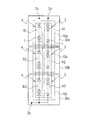
- the conventional light-emitting device includes a plurality of light-emitting blocks C1 to C7.
- Each of the light-emitting blocks includes two to four LED elements which are connected in series.
- the light-emitting blocks C1 to C7 are arranged in any shape to display a character and so on.
- an object of the conventional light-emitting device is to display a character and so on by properly arranging a plurality of light-emitting blocks, a drive condition, light-emitting intensity and so on of the light-emitting blocks are not at all disclosed.
- the conventional light-emitting device does not disclose a light-emitting device including a plurality of light-emitting areas that can emit uniform light from each respective light-emitting areas of the light-emitting device, even if light-emitting elements included in the light-emitting device are driven by the voltage rectified from an AC voltage that continuously changes from low value to high value and from high value to low value like a continuous wave.
- the invention provides a light-emitting device including a plurality of light-emitting areas each with a first light-emitting block and a second light-emitting block.
- the first light-emitting block of each respective light-emitting areas include first light-emitting elements to be lit at a first voltage value
- the second light-emitting blocks of the light-emitting areas include the second light-emitting elements to be lit at a second voltage value that is set higher than the first voltage, while the first light-emitting elements are kept lit at voltages on and above the first voltage value.
- a light-emitting device includes a plurality of light-emitting areas each including a first light-emitting block and a second light-emitting block, and the plurality of first light-emitting blocks each include a plurality of first light-emitting elements, and the plurality of second light-emitting blocks each include a plurality of second light-emitting elements.
- the light-emitting device further includes a control circuit that includes at least one switch switching a voltage supply to the first light-emitting elements in the plurality of light-emitting areas or to the second light-emitting elements in the plurality of light-emitting areas as well as the first light-emitting elements in the plurality of light-emitting areas.
- control circuit includes two switches, a first switch is configured to switch a voltage supply to the first light-emitting elements in the first light-emitting blocks of the plurality of light-emitting areas and a second switch is configured to switch the voltage supply to the second light-emitting elements in the second light-emitting blocks of the plurality of light-emitting areas as well as the first light-emitting elements in the first light-emitting blocks of the plurality of light-emitting areas.
- the control circuit is configured to detect value of voltage rectified from an AC voltage of the AC power source and to switch the first switch to apply the voltage to the first light-emitting elements in the first light-emitting blocks when the voltage being supplied from the AC power source reaches a first voltage value, and the control circuit is configured to switch the second switch to apply the voltage to the second light-emitting elements of the second light-emitting blocks as well as the first light-emitting elements in the first light-emitting blocks when the voltage being supplied from the AC power source reaches a second voltage value that is set higher than the first voltage value.
- the light-emitting device that emits uniform light from each respective light-emitting areas in accordance with changes of voltage can be achieved.
- the first light-emitting elements and the second light-emitting elements are driven by the voltage rectified from an AC voltage that continuously changes from low value to high value and from high value to low value like a continuous wave, as each respective light-emitting areas include the first light-emitting block and the second light-emitting block, the light-emitting areas can emit uniform light in accordance with the value of voltage that changes continuously. Also, the light-emitting device with simple electrical connection can be proposed.
- Fig. 1 is a perspective view showing a light-emitting device according to a first embodiment of the present invention.
- Fig. 2 is an arrangement view of a light-emitting block in each of light-emitting areas of the light-emitting device as shown in Fig. 1.
- Fig. 3-A is a sectional view taken along line A-A of the light-emitting device as shown in Fig. 1.
- Fig. 3-B is a schematic view showing a modified example of an arrangement of the light-emitting areas.
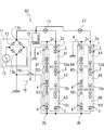
- Fig. 4 is a system block view showing a control circuit of the light-emitting device as shown in Fig. 1.
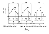
- 5-A is a wave shape view showing a relationship a current and a light-emitting time of the light-emitting areas in the light-emitting device as shown in Fig. 1.
- Fig. 5-B is a wave shape view showing a relationship a light flux and a light-emitting time of the light-emitting areas in the light-emitting device as shown in Fig. 1.
- Fig. 6 is a perspective view of a light-emitting device according to a second embodiment of the present invention.
- Fig. 7 is an arrangement view of a light-emitting block in each of light-emitting areas of the light-emitting device as shown in Fig. 6.
- FIG. 8 is a system block view showing a control circuit of a light-emitting device according to a third embodiment of the present invention.
- Fig. 9 is another system block view showing a control circuit of a light-emitting device according to a fourth embodiment of the present invention.
- Fig. 10 is a plan view showing a conventional light-emitting device.
- Figs. 1 to 5 illustrate a light-emitting device 10 according to a first embodiment of the present invention.
- the light-emitting device 10 includes a first light-emitting area 10a that includes a first light-emitting block 3 and a second light-emitting block 4.
- the first light-emitting block 3 includes first light-emitting elements A1 that are electrically connected to one another of the first light-emitting elements A1 in the first light-emitting block 3 in series.
- the second light-emitting elements B1 in the second light-emitting block 4 are electrically connected to one another of the second light-emitting elements B1 in the second light-emitting block 4 in series.
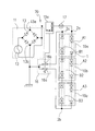
- the light-emitting device 10 also includes a control circuit 60 including a first switch 16a that switches a voltage supply rectified from an alternative current (AC) power source 12 to the first light-emitting elements A1, and the control circuit 60 includes a second switch 16b that switches the voltage supply rectified from the AC power source to the second light-emitting elements B1 as well as the first light-emitting elements A1.
- a control circuit 60 including a first switch 16a that switches a voltage supply rectified from an alternative current (AC) power source 12 to the first light-emitting elements A1
- AC alternative current
- the control circuit 60 includes a voltage level detecting circuit 15 that can be connected to the power source terminals 13a and 13b of a rectifier 13 and a switching circuit 16, and the control circuit 60 is configured to detect voltage value rectified from an AC voltage of the AC power source and to switch the first switch 16a to apply the voltage to the first light-emitting elements A1, A2, and A3 when the voltage being supplied from the AC power source 11 reaches a first voltage value LV1 and configured to switch the second switch 16b to apply the voltage to the second light-emitting elements B1 as well as the first light-emitting elements A1 when the voltage being supplied from the AC power source 12 reaches a second voltage value HV1 that is set higher than the first voltage value LV1.
- a rectifier 13 is used to rectify the AC voltage and to apply the voltage that is rectified by the rectifier 13 to light-emitting elements.
- a plurality of light-emitting areas can emit light equally with one another of the light-emitting areas.
- the first voltage value LV1 and the second voltage value HV1 should be set in consideration of the AC power voltage of a targeted country where the light-emitting device 10 will be used, a necessary number of light-emitting areas 10a, 10b, 10c, and more, the number of the first light-emitting elements A1, and the number of the second light-emitting elements B1.
- AC power voltage is around 220V.
- a light-emitting element generally requires around 3V to emit light.
- a light-emitting device 10 includes five light-emitting areas
- the total number of the first light-emitting elements could be 30 and the total number of the second light-emitting elements could be 20 that are divided into the five light-emitting areas each with six first-light-emitting elements and four second-light-emitting elements.
- the first voltage value LV1 is set to be 90V (3V*6*5)
- the second voltage value HV1 is set to be 150V (3V*6*5+3V*4*5).
- the first voltage value LV1 in this case, the first voltage value is 90V
- the first light-emitting elements A1 in the first light-emitting blocks of the five light-emitting areas start to emit light
- the second voltage value HV1 in this case, the second voltage value is 150V
- the second light-emitting elements in the second light-emitting blocks of the five light-emitting areas start to emit light.
- the first light-emitting elements are lit while the voltage being supplied from the AC power source is at and above 90V
- the second light-emitting elements B1 are lit while the voltage being supplied from the AC power source is at and above 150V.
- the first voltage value LV1 and the second voltage value HV1 change in accordance with a targeted country's AC power voltage, the number of light-emitting areas, and the total number of the first light-emitting elements and the total number of the second light-emitting elements, they can be set in consideration of above mentioned conditions.
- first light-emitting area 10a there are three light-emitting areas; a first light-emitting area 10a, a second light-emitting area 10b, and a third light-emitting area 10c.
- a first light-emitting block 3 and a second light-emitting block 4 in each respective first light-emitting area 10a, second light-emitting area 10b and third light-emitting area 10c are arranged side by side.
- the first light-emitting area 10a further includes a first circuit substrate 30a at that the first light-emitting elements and the second light-emitting elements of the first light-emitting area 10a are mounted.
- the second light-emitting area 10b includes a second circuit substrate 30b, and the first light-emitting elements A2 of the second light-emitting area are disposed at the second circuit substrate 30b and the second light-emitting elements B2 of the second light-emitting area are disposed at the second circuit substrate 30b.
- the third light-emitting area 10c includes a third circuit substrate 30c, and the first light-emitting elements A3 of the third light-emitting area are disposed at the third circuit substrate 30c and the second light-emitting elements B3 of the third light-emitting area 10c are disposed at the third circuit substrate 30c.
- the number of the first light-emitting elements and the number of the second light-emitting elements are different from one another of the first light-emitting elements and the second light-emitting elements of each respective first, second, third light-emitting areas. Also, the number of the first light-emitting elements in each of the first light-emitting area, the second light-emitting area, and the third light-emitting area is the same with one another of the first light-emitting area, the second light-emitting area, and the third light-emitting area, and the number of the second light-emitting elements in each of the first light-emitting area, the second light-emitting area, and the third light-emitting area is the same with one another of the first light-emitting area, the second light-emitting area, and the third light-emitting area.
- the first light-emitting block 3 in each respective first light-emitting area 10a, second light-emitting area 10b and third light-emitting area 10c includes first light-emitting elements A1, A2, and A3, and the second light-emitting block 4 in each respective first light-emitting area 10a, second light-emitting area 10b and third light-emitting area 10c includes second light-emitting elements B1, B2, and B3.
- the first light-emitting elements A1 of the first light-emitting area 10a are electrically connected in series to the first light-emitting elements A2 of the second light-emitting area 10b
- the first light-emitting elements A2 of the second light emitting area 10b are electrically connected in series to the first light-emitting elements A3 of the third light-emitting area 10c
- the first light-emitting elements A3 of the third light-emitting area 10c are electrically connected in series to the second light-emitting elements B3 of the third light-emitting area 10c
- the second light-emitting elements B3 of the third light-emitting area 10c are electrically connected in series to the second light-emitting elements B2 of the second light-emitting area 10b
- the second light-emitting elements B2 of the second light-emitting area 10b are electrically connected in series to the second light-emitting elements B1 of the first light-emitting
- the control circuit including the switch that switches the voltage to the second light-emitting elements as well as the first light-emitting elements when the voltage being supplied from the AC power source reaches the second voltage value with a simple connection.
- the light-emitting device 10 may further include a rectifier 13 that can be electrically connected to the AC power source 12 to rectify an AC voltage of the AC power source 12 and supply the voltage that is rectified to the first light-emitting elements and the second light-emitting elements through the control circuit.
- a rectifier 13 that can be electrically connected to the AC power source 12 to rectify an AC voltage of the AC power source 12 and supply the voltage that is rectified to the first light-emitting elements and the second light-emitting elements through the control circuit.
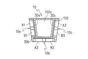
- the light-emitting device 10 can be used as a street light 100 as an example.
- the street light 100 includes a casing 102 that includes a first surface, a second surface, and a third surface, and the first light-emitting area 10a is disposed at the first surface of the casing 102, the second light-emitting area 10b is disposed at the second surface of the casing 102, and the third light-emitting area 10c is disposed at the third surface of the casing 102.
- the casing 102 may include a polyhedral shape with polyhedral surfaces.
- the casing 102 includes a space 102a inside the casing 102, a first end portion 102b at that the light-emitting areas 10a, 10b, and 10c are disposed, and a second end portion 102c.
- the first end portion 102b and the second end portion 102c are laterally opposite to each other.
- the casing 102 may further include a support 101 that supports the second end portion 102c of the casing 102.
- the casing 102 may have an inverted trapezoidal shape.
- first light-emitting area 10a there are the first light-emitting area 10a, the second light-emitting area 10b and the third light-emitting area 10c are arranged at respective surfaces in the space 102a of the casing 12.
- the first light-emitting area 10a, the second light-emitting area 10b, and the third light-emitting area 10c may be arranged at, at least some of polyhedral surfaces of the casing 102 to emit light outside the casing 102 in different directions.
- a first surface and the second surface of the casing 102 may be disposed with a first angle between the first surface and the second surface, and the second surface and the third surface of the casing 102 may be disposed with a second angle between the second surface and the third surface.
- the first angle and the second angle may be the same with each other or may be different from each other in accordance with the shape of the casing 102.
- a fourth surface or more surfaces may be provided for additional light-emitting areas 10a, 10b, and 10c.
- the first light-emitting area 10a and the third light-emitting area 10c are attached to inner walls of right and left surfaces at the first end portion 102b of the casing 102, and the second light-emitting area 10b is attached to a front surface positioned between the inner walls of the right and left surfaces at the first end portion 102b of the casing 102.
- These first to third light-emitting areas 10a to 10c are configured to emit light in respective directions outside the casing 102. Accordingly, a street or a space can be illuminated widely.
- the first embodiment it is also possible to achieve a light-emitting device that also emits light downward with a fourth light-emitting area on a bottom surface positioned between the inner walls of the right and left surfaces in the first end portion 102b of the casing 102, for example.
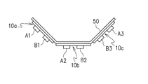
- Fig. 3A and 3B illustrates a modified example of the first light-emitting area 10a including a first circuit substrate 30a, the second light-emitting area 10b including a second circuit substrate 30b and the third light-emitting area 10c including a third circuit substrate 30c.
- the first circuit substrate 30a, the second circuit substrate 30b and the third circuit substrate 30c are arranged on a metal plate 50 including three surfaces with a predetermined angle between respective adjacent surfaces of the three surfaces of the metal plate 50.
- the metal plate 50 can be arranged on a wall of a building and/or in such a casing 102 of a light-emitting device. In this way, the plurality of light-emitting areas 10a, 10b and 10c can be applied to various light-emitting devices and systems.
- the first light-emitting area 10a may include the first light-emitting block 3 and the second emitting block 4 arranged side by side
- the second light-emitting area 10b may include the first light-emitting block 3 and the second emitting block 4 arranged side by side
- the third light-emitting area 10c may include the first light-emitting block 3 and the second emitting block 4 arranged side by side.
- the first circuit substrate 30a may be provided on a first metal plate
- the second circuit substrate 30b may be provided on a second metal plate
- the third circuit substrate 30c may be provided on a third metal plate, separately.
- the first light-emitting elements A1 and the second light-emitting elements B1 of the first light-emitting area are mounted at the first circuit substrate 30a and thermally connected to the first metal plate
- the first light-emitting elements A2 and the second light-emitting elements B2 of the second light-emitting area are mounted at the second circuit substrate 30b and thermally connected to the second metal plate
- the first light-emitting elements A3 and the second light-emitting elements B3 of the third light-emitting area are mounted at the third circuit substrate 30c and thermally connected to the third metal plate.
- the first light-emitting block 3 and the second light-emitting block 4 are electrically connected to a first electrode 2a and a third electrode 2c which are provided on the circuit substrate 30a and a second electrode 2b which is provided on the circuit substrate 30c.
- the constitution is mentioned below.
- Fig. 4 illustrates an example of electrical connection, showing a system block view of a control circuit including a first switch 16a and a second switch 16b.
- the first light-emitting block 3 and the second light-emitting block 4 are electrically connected in series to the first electrode 2a, the second electrode 2b, and the third electrode 2c.
- the first light-emitting elements A1, A2, A3 of the first light-emitting blocks 3 are electrically connected in series to the first electrode 2a and the second electrode 2b.
- the second light-emitting elements B1, B2, B3 of the second light-emitting blocks 4 are electrically connected in series to the second electrode 2b and the third electrode 2c.
- the control circuit 60 includes the first switch 16a that switches the voltage supply from the AC power source to the first light-emitting elements A1, A2, A3 and the second switch 16b, and the second switch 16b that switches the voltage supply from the AC power source 12 to the second light-emitting elements B1, B2, B3 as well as the first light-emitting elements A1, A2, A3.
- the control circuit 60 is configured to detect value of voltage rectified from an AC voltage of the AC power source 12 and to switch the first switch 16a to apply the voltage to the first light-emitting elements A1, A2, A3 when the voltage being supplied from the AC power source 12 reaches the first voltage value LV1, and the control circuit 60 is configured to switch the second switch 16b to apply the voltage to the second light-emitting elements B1, B2, B3 as well as the first light-emitting elements A1, A2, A3 when the voltage being supplied from the AC power source 12 reaches the second voltage value HV1 that is set higher than the first voltage value LV1.
- the voltage is flowed from the first electrode 2a, through the first light-emitting elements A1, A2, A3 in the first light-emitting blocks 3 to the second electrode 2b during the voltage supply from the AC power source 12 remaining below the second voltage value HV1, and the control circuit 60 that controls to apply the voltage is flowed from the first electrode 2a, through the first light-emitting elements A1, A2, A3 in the first light-emitting blocks 3 to the second electrode 2b, and further through the second light-emitting elements B1, B2, B3 in the second light-emitting blocks 4 to the third electrode 2c.
- an AC (alternating-current) power source 12 is shown in the system blocks of Figures 4, 8, and 9, the AC power source 12 is not included in this light-emitting device 10.
- the AC power source 12 is basically located outside the light-emitting device 10, for example, in a building or a facility, and the light-emitting device 10 uses the voltage that is rectified from the AC voltage of the AC power source 12 to drive light-emitting elements. Accordingly, the light-emitting device 10 includes a rectifier 13 to rectify an AC voltage and supply a voltage that is rectified from the AC voltage to the first light-emitting elements and the second light-emitting elements through the control circuit 60.
- the rectifier 13 can perform full-wave rectification for a pulse wave signal (hereinafter referred to as AC voltage) to supply a rectified voltage or a DC voltage.
- AC voltage a pulse wave signal
- AC 120V and 60Hz an AC power source of AC 120V and 60Hz is explained.
- the light-emitting device 10 includes a control circuit 60 that includes a voltage level detecting circuit or voltage level detector circuit 15 connected to the power source terminals 13a and 13b of the rectifier 13 and detects a value of AC voltage level (high voltage HV, low voltage LV).
- the control circuit 60 also includes a switching circuit 16 that includes a first switch 16a and a second switch 16b. The first switch 16a switches a voltage supply to the first light-emitting elements and the second switch 16b switches the voltage supply to the second light-emitting elements as well as the first light-emitting elements.
- the first switch 16a and the second switch 16b are configured to be switched by a detection signal of the voltage level detecting circuit 15 and is configured to switchably connect the second electrode 2b and the third electrode 2c to the power source terminal 13b of the rectifier 13.
- the power source terminal 13a of the rectifier 13 is connected through a current-limiting element 17 (for example, a resistive element) to the first electrode 2a.
- the first light-emitting block 3 is lighted, and in this state, when the power source terminal 13b of the rectifier 13 is connected to the third electrode 2b, the second light-emitting block 4 is lighted.
- the switching circuit 16 While the voltage level detecting circuit 15 detects a low voltage level LV, the switching circuit 16 is maintained in a state where the first switch 16a is ON and the second switch 16b is OFF. On the other hand, while the voltage level detecting circuit 15 detects a high voltage level HV including a peak of the AC voltage supply, the switching circuit 16 is switched to a state where the first switch 16a is OFF and the second switch 16b is ON.
- the first light-emitting block 3 is connected between the power source terminals 13a and 13b of the rectifier 13, thereby the first light-emitting elements A1, A2 and A3 constituting the first light-emitting block 3 are lighted.
- each of the three light-emitting areas 10a, 10b and 10c has the same light-emitting intensity, that is, brightness, because each of the first light-emitting elements A1, A2 and A3 has the same number of light-emitting elements, as mentioned above.
- the switching circuit 16 when the switching circuit 16 is switched to a state where the first switch 16a is OFF and the second switch 16b is ON, the power source terminal 13a of the rectifier 13 is connected through the current-limiting element 17 to the first electrode 2a of the light-emitting device 10 and a current flowing in first light-emitting elements in the first light-emitting blocks 3 flows from the second electrode 2b into the second light-emitting elements in the second light-emitting blocks 4, and then flows from the third electrode 2c into the power source terminal 13b of the rectifier 13 through the second switch 16b that is in a state of ON.
- the first light-emitting block 3 and the second light-emitting block 4 are connected in series between the power source terminals 13a and 13b of the rectifier 13. Consequently, the first light-emitting elements A1, A2, and A3 in the first light-emitting blocks 3 and the second light-emitting elements B1, B2, and B3 in the second light-emitting blocks 4 are lighted.
- the voltage level detecting circuit 15 detects the first voltage value that is the low voltage level LV1, the first light-emitting elements A1, A2 and A3 constituting the first light-emitting blocks 3 are lighted, and while the voltage level detecting circuit 15 detects the second voltage value that is high voltage level HV1 including a peak of the AC voltage supply, the second light-emitting elements B1, B2 and B3 constituting the second light-emitting blocks 4 are lighted, in addition to the first light-emitting elements A1, A2, and A3 in the first light-emitting blocks 3.
- the number of the light-emitting elements constituting the first light-emitting elements A1, A2 and A3 and the number of the light-emitting elements constituting the second light-emitting elements B1, B2 and B3 are the same, light emitted from the first light-emitting elements A1, A2 and A3 and light emitted from the second light-emitting elements B1, B2 and B3 have the same brightness.
- a light-emitting time of the first light-emitting block 3 depends on the number of the light-emitting elements 1 serially arranged in the first light-emitting block 3, and a light-emitting time of the second light-emitting block 4 depends on the number of the light-emitting elements serially arranged in the second light-emitting block 4.
- the number of each of the first light-emitting elements A1, A2 and A3 in the first light-emitting block 3 is thirty (30)
- the number of each of the second light-emitting elements B1, B2 and B3 in the second light-emitting block 4 is twenty (20).
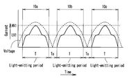
- Fig. 5A illustrates a drive current of each of the first light-emitting block 3 and the second light-emitting block 4, which are driven by the voltage rectified from an AC voltage.
- a vertical axis shows a current and a horizontal axis shows a time.
- a wave shape shown by solid line shows a light-emitting period T in each of the first to third light-emitting areas 10a, 10b and 10c, and a wave shape shown by dotted line shows the voltage in each of the first to third light-emitting areas 10a, 10b and 10c. Further details are described with reference to Fig. 5B.
- the voltage wave shape repeats mountain-like pulse wave shape because the rectified voltage from the AC voltage is used, and until the detection level of the voltage level detecting circuit 15 as shown by the vertical axis reaches LV1, a current flows only the first light-emitting block 3. Consequently, only the first light-emitting block 3 is lighted at the first voltage value.
- a current flows in the series connection between the first light-emitting block 3 and the second light-emitting block 4, thereby the first light-emitting block 3 and the second light-emitting block 4 are lighted.
- a period in which the first light-emitting block 3 and the second light-emitting block 4 are lighted by a current flowing therein is the light-emitting period T. Because a current does not flow in the first light-emitting block 3 while the voltage is lower than a threshold voltage of the first light-emitting block 3, this period is a non-light-emitting period T 0 in which the light emission is not performed.
- Fig. 5B illustrates a light-emitting wave shape KH of the each of the light-emitting areas 10a, 10b and 10c.
- the light-emitting wave shape KH of each of the first to third light-emitting areas 10a, 10b and 10c has approximately the same shape as a wave shape of the drive current.
- the light-emitting condition with respect to the plurality of light-emitting areas represents the constantly same light-emitting state and the same drive current flowing in each light-emitting element, regardless of the switching conditions due to the AC voltage of the AC power supply. Therefore, it is possible to provide a light-emitting device including a plurality of light-emitting areas with a simple electrical connection. Accordingly, the light-emitting device can have the light-emitting areas with uniform intensity of light and operating life maintained, even if the light-emitting elements in the light-emitting device will be driven by the voltage rectified from an AC voltage.
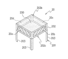
- a light-emitting device according to a second embodiment of the present invention is described with reference to Figs. 6 and 7.
- the light-emitting device 20 includes a support 201, and a casing 202 provided on an upper end of the support 201 and including a first end portion 202b and a second end portion 202c vertically opposite to each other, and peripheral surfaces between the first end portion 202b and the second end portion 202c.
- the light-emitting areas 20a, 20b, 20c and 20d are disposed at, at least some of the peripheral surfaces of the casing 202.
- the support supports the casing at the second end portion 202c.
- the support may include a plurality of pillars 203.
- Fig. 6 illustrates an example in which the light-emitting device 20 according to the present invention is applied to an illumination device 200 set in a building or outside.
- the illumination device 200 has a squire shape and includes four surfaces at a circumference of the device.
- First light-emitting area 20a, second light-emitting area 20b, third light-emitting area 20c and fourth light-emitting area 20d are arranged on the four surfaces of the illumination device, respectively.
- Fig. 7 illustrates a light-emitting block 23 and a second light-emitting block 24 in the light-emitting device 20.
- the light-emitting device 20 in the second embodiment has the same basic structure as the light-emitting device 10 in the first embodiment. Accordingly, only a difference of the light-emitting device in the second embodiment from the light-emitting device according to the first embodiment is explained.
- the light-emitting device 20 in the second embodiment differs from the light-emitting device 10 in the first embodiment in that the light-emitting device 20 includes four light-emitting areas 20a, 20b, 20c and 20d, as shown in Figs. 6 and 7. Consequently, in the light-emitting device 20 according to the second embodiment, the first light-emitting block 23 includes four first light-emitting elements A1, A2, A3 and A4, and the second light-emitting block 4 includes four second light-emitting elements B1, B2, B3 and B4.
- each of the first light-emitting elements A1, A2, A3 and A4 constituting the first light-emitting block 23 has the same number of light-emitting elements 1
- each of the second light-emitting elements B1, B2, B3 and B4 constituting the second light-emitting block 24 has the same number of light-emitting elements 1.
- each of the first and second light-emitting elements A1 and B1 arranged in the first light-emitting area 20a, the first and second light-emitting elements A2 and B2 arranged in the second light-emitting area 20b, the first and second light-emitting elements A3 and B3 arranged in the third light-emitting area 20c, and the first and second light-emitting elements A4 and B4 arranged in the fourth first light-emitting area 20d is formed by the same number of light-emitting elements 1.
- each of the first light-emitting elements A1, A2, A3, A4 and the second light-emitting elements B1, B2, B3 and B4 in the light-emitting areas 20a, 20b, 20c and 20d is configured by the same number and the same arrangement of the light-emitting elements 1.
- a light-emitting wave shape KH of each of the light-emitting areas 20a, 20b, 20c and 20d has approximately the same shape as a wave shape of a drive current, similarly to the wave shape views shown in Figs. 5A and 5B.
- the light-emitting condition with respect to the plurality of light-emitting areas indicates the constantly same light-emitting state and the same drive current flowing in each light-emitting element, regardless of the switching conditions of the AC power supply. Therefore, it is possible to provide a light-emitting device in which there is no difference in the drive condition, thereby the same illumination effect and the same operating life are maintained.
- the light-emitting device in the third embodiment has a structure adapted to drive the aforementioned light-emitting device 10 by a voltage level-switching system.
- Fig. 8 illustrates a system of a drive circuit of the light-emitting device 10. Because a control circuit 70 as shown in Fig. 8 is basically the same as the control circuit 60 shown in Fig. 4, in the light-emitting device in the third embodiment, identical reference numbers are attached to similar parts to that in the light-emitting device 10 in the first embodiment, as a result, a duplicated description thereof is omitted.
- the control circuit as shown in Fig. 8 differs from the control circuit as shown in Fig. 4 in the following points.
- the switching circuit 16 to perform the switching connection of the first light-emitting block 3 and the second light-emitting block 4 is controlled based on the voltage level detection of the voltage level detecting circuit 15, but in the control circuit 70 of the current level-switching system as shown in Fig. 8, the control circuit 70 is controlled based on the current level detection of a current level detecting circuit 15a.
- the current level detecting circuit 15a controls a current based on the detection signal of the current level LA, HA to perform light-emitting operation of the light-emitting device 10.
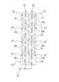
- the light-emitting device 10 with more light-emitting areas can be provided with a simple electrical connection. As shown in Fig. 9, there are six light-emitting areas 10a-10f each with a first light-emitting block 3 and a second light-emitting block 4. As a light-emitting device, the light-emitting device includes the plurality of light-emitting areas 10a-10f each including a first light-emitting block 3 and a second light-emitting block 4.
- the plurality of first light-emitting blocks 3 each include a plurality of first light-emitting elements A1, A2, A3, A4, A5 or A6, and the plurality of second light-emitting blocks 4 each include a plurality of second light-emitting elements B1, B2, B3, B4, B5 or B6.
- the light-emitting device further includes a control circuit 80 that including a switch 16c that switches a voltage to the first light-emitting elements A1-A6 and to the second light-emitting elements B1-B6.
- the voltage rectified from the AC power source 12 by a rectifier 13 is applied to the first light-emitting elements A1-A6 that are configured to start light at a first voltage value LV1
- the control circuit 80 is configured to switch the switch 16c to apply the voltage to the second light-emitting elements B1-B6 as well as the first light-emitting elements A1-A6 when the voltage reaches a second voltage value HV1 that is set higher than the first voltage value LV1.
- the control circuit 80 includes a voltage level detecting circuit 15 that can be connected to the power source terminals 13a and 13 b of the rectifier 13 and a switching circuit 16 including the single switch 16c.
- the first light-emitting elements in the first light-emitting block of each respective first light-emitting areas are electrically connected to one another of the first light-emitting elements in the first light-emitting block 3 in series, and the second light-emitting elements in the second light-emitting block 4 of each respective first light-emitting areas electrically connected to one another of the second light-emitting elements in the second light-emitting block 4 in series.
- the first light-emitting elements (A1 or A4) of the first light-emitting area (10a or 10d) are electrically connected in series to the first light-emitting elements (A2 or A5) of the second light-emitting area (10b or 10e)
- the first light-emitting elements (A2 or A5) of the second light emitting area (10b or 10e) are electrically connected in series to the first light-emitting elements (A3 or A6) of the third light-emitting area (10c or 10f)
- the first light-emitting elements (A3 or A6) of the third light-emitting area (10c or 10f) are electrically connected in series to the second light-emitting elements (B3 or B6) of the third light-emitting area (10c or 10f)
- the light-emitting areas 10a-10f can emit a same or similar intensity of light with one another even when the voltage from the AC power source changes from a low voltage to a high voltage or from a high voltage to a low voltage.
- illumination light of each light-emitting area has constantly the same brightness, and each light-emitting element in each light-emitting area has the same service life.
- the present invention is applied to the light-emitting device using the light-emitting diode elements as the light-emitting elements, the present invention may be applied to a light-emitting device using light-emitting elements other than the light-emitting diode elements.
Landscapes
- Engineering & Computer Science (AREA)
- Physics & Mathematics (AREA)
- Microelectronics & Electronic Packaging (AREA)
- Optics & Photonics (AREA)
- General Engineering & Computer Science (AREA)
- Circuit Arrangement For Electric Light Sources In General (AREA)
- Arrangement Of Elements, Cooling, Sealing, Or The Like Of Lighting Devices (AREA)
- Non-Portable Lighting Devices Or Systems Thereof (AREA)
- Led Device Packages (AREA)
- Led Devices (AREA)
Priority Applications (5)
| Application Number | Priority Date | Filing Date | Title |
|---|---|---|---|
| JP2010294507A JP2012142453A (ja) | 2010-12-29 | 2010-12-29 | 半導体発光装置 |
| US13/822,792 US9241383B2 (en) | 2010-12-29 | 2011-12-29 | Light-emitting device |
| DE112011104649T DE112011104649T5 (de) | 2010-12-29 | 2011-12-29 | Licht aussendende Vorrichtung |
| CN201180063701.4A CN103314456B (zh) | 2010-12-29 | 2011-12-29 | 发光装置 |
| JP2013529250A JP5858494B2 (ja) | 2010-12-29 | 2011-12-29 | 発光装置 |
Applications Claiming Priority (2)
| Application Number | Priority Date | Filing Date | Title |
|---|---|---|---|
| JP2010-294507 | 2010-12-29 | ||
| JP2010294507A JP2012142453A (ja) | 2010-12-29 | 2010-12-29 | 半導体発光装置 |
Publications (2)
| Publication Number | Publication Date |
|---|---|
| WO2012090509A2 true WO2012090509A2 (en) | 2012-07-05 |
| WO2012090509A3 WO2012090509A3 (en) | 2013-01-31 |
Family
ID=46383592
Family Applications (1)
| Application Number | Title | Priority Date | Filing Date |
|---|---|---|---|
| PCT/JP2011/007369 Ceased WO2012090509A2 (en) | 2010-12-29 | 2011-12-29 | Light-emitting device |
Country Status (5)
| Country | Link |
|---|---|
| US (1) | US9241383B2 (enExample) |
| JP (2) | JP2012142453A (enExample) |
| CN (1) | CN103314456B (enExample) |
| DE (1) | DE112011104649T5 (enExample) |
| WO (1) | WO2012090509A2 (enExample) |
Families Citing this family (2)
| Publication number | Priority date | Publication date | Assignee | Title |
|---|---|---|---|---|
| CN109716863B (zh) * | 2016-05-02 | 2021-08-27 | 亮锐控股有限公司 | 具有带分接头的线性驱动器的多焊盘多接点led封装 |
| WO2020211044A1 (en) * | 2019-04-18 | 2020-10-22 | Boe Technology Group Co., Ltd. | Display substrate, display apparatus, and method of fabricating display substrate |
Family Cites Families (15)
| Publication number | Priority date | Publication date | Assignee | Title |
|---|---|---|---|---|
| JP2005183721A (ja) | 2003-12-19 | 2005-07-07 | Touken Techno:Kk | Led照明装置 |
| JP4581646B2 (ja) | 2004-11-22 | 2010-11-17 | パナソニック電工株式会社 | 発光ダイオード点灯装置 |
| JP4588494B2 (ja) | 2005-03-03 | 2010-12-01 | 株式会社ジャムコ | 照明用発光ダイオード駆動回路 |
| JP4785586B2 (ja) * | 2006-03-23 | 2011-10-05 | アルパイン株式会社 | Ledバックライト駆動装置 |
| KR101340905B1 (ko) * | 2006-05-02 | 2013-12-13 | 코닌클리케 필립스 엔.브이. | 발광 다이오드 회로, 배열 및 장치 |
| JP5007395B2 (ja) * | 2006-06-23 | 2012-08-22 | シーシーエス株式会社 | 立体光源体 |
| JP5319933B2 (ja) * | 2008-02-26 | 2013-10-16 | パナソニック株式会社 | 照明装置 |
| JP2010225413A (ja) | 2009-03-24 | 2010-10-07 | Nippon Seiki Co Ltd | 照明装置 |
| US8410717B2 (en) * | 2009-06-04 | 2013-04-02 | Point Somee Limited Liability Company | Apparatus, method and system for providing AC line power to lighting devices |
| TW201044912A (en) * | 2009-06-08 | 2010-12-16 | Univ Nat Cheng Kung | Driving device |
| US8384307B2 (en) * | 2009-06-16 | 2013-02-26 | Nexxus Lighting, Inc. | Continuous step driver |
| US7936135B2 (en) * | 2009-07-17 | 2011-05-03 | Bridgelux, Inc | Reconfigurable LED array and use in lighting system |
| US8384311B2 (en) * | 2009-10-14 | 2013-02-26 | Richard Landry Gray | Light emitting diode selection circuit |
| US8299724B2 (en) * | 2010-03-19 | 2012-10-30 | Active-Semi, Inc. | AC LED lamp involving an LED string having separately shortable sections |
| US8040071B2 (en) * | 2010-12-14 | 2011-10-18 | O2Micro, Inc. | Circuits and methods for driving light sources |
-
2010
- 2010-12-29 JP JP2010294507A patent/JP2012142453A/ja active Pending
-
2011
- 2011-12-29 US US13/822,792 patent/US9241383B2/en not_active Expired - Fee Related
- 2011-12-29 WO PCT/JP2011/007369 patent/WO2012090509A2/en not_active Ceased
- 2011-12-29 DE DE112011104649T patent/DE112011104649T5/de not_active Withdrawn
- 2011-12-29 CN CN201180063701.4A patent/CN103314456B/zh not_active Expired - Fee Related
- 2011-12-29 JP JP2013529250A patent/JP5858494B2/ja not_active Expired - Fee Related
Also Published As
| Publication number | Publication date |
|---|---|
| JP5858494B2 (ja) | 2016-02-10 |
| US9241383B2 (en) | 2016-01-19 |
| US20130264958A1 (en) | 2013-10-10 |
| JP2012142453A (ja) | 2012-07-26 |
| WO2012090509A3 (en) | 2013-01-31 |
| DE112011104649T5 (de) | 2013-09-26 |
| CN103314456A (zh) | 2013-09-18 |
| CN103314456B (zh) | 2016-09-28 |
| JP2014506373A (ja) | 2014-03-13 |
Similar Documents
| Publication | Publication Date | Title |
|---|---|---|
| JP5725736B2 (ja) | Led電源装置及びled照明器具 | |
| US8360609B2 (en) | Illumination apparatus and driving method thereof | |
| KR101267278B1 (ko) | 변조지수가 개선된 엘이디 조명장치 | |
| JP5665382B2 (ja) | Led電源装置及びled照明器具 | |
| US20140062313A1 (en) | Lighting device and lighting fixture using the same | |
| JP2011258589A (ja) | Ledランプ装置 | |
| KR101435853B1 (ko) | 발광 다이오드 구동 장치 | |
| CN105530740A (zh) | 调光控制单元、照明系统和设施设备 | |
| JP5538078B2 (ja) | Led電源装置 | |
| US9775214B2 (en) | Battery backup system for LED luminaire | |
| JP2017054653A (ja) | 点灯装置、照明装置、および照明器具 | |
| KR100287781B1 (ko) | 발광다이오드를이용한전등회로및전등구조 | |
| WO2012090509A2 (en) | Light-emitting device | |
| KR20140070289A (ko) | 변조지수가 개선된 엘이디 조명장치 | |
| US8143793B2 (en) | Device and method for periodic diode actuation | |
| JP2009245638A (ja) | 制御装置、当該制御装置を備える照明装置 | |
| KR101431614B1 (ko) | 발광 다이오드 조명등 및 발광 다이오드 조명 장치 | |
| CN110072313B (zh) | Led照明装置 | |
| JP2001268760A (ja) | 架線装着形照明灯 | |
| JP2009129136A (ja) | 照明制御装置及びそれを備えた自動販売機 | |
| JP2004252342A (ja) | 発電量表示装置 | |
| JP2012028506A (ja) | Led点灯装置 | |
| JP2001148293A (ja) | 灯器システム | |
| KR102003365B1 (ko) | Led 구동 장치 | |
| KR101592111B1 (ko) | 물체 감지를 통한 자동 밝기 조절기능을 갖는 엘이디 조명장치 및 그것의 엘이디 어레이 구조 |
Legal Events
| Date | Code | Title | Description |
|---|---|---|---|
| WWE | Wipo information: entry into national phase |
Ref document number: 13822792 Country of ref document: US |
|
| ENP | Entry into the national phase |
Ref document number: 2013529250 Country of ref document: JP Kind code of ref document: A |
|
| WWE | Wipo information: entry into national phase |
Ref document number: 112011104649 Country of ref document: DE Ref document number: 1120111046499 Country of ref document: DE |
|
| 122 | Ep: pct application non-entry in european phase |
Ref document number: 11853201 Country of ref document: EP Kind code of ref document: A2 |