WO2012086142A1 - 検査装置 - Google Patents
検査装置 Download PDFInfo
- Publication number
- WO2012086142A1 WO2012086142A1 PCT/JP2011/006836 JP2011006836W WO2012086142A1 WO 2012086142 A1 WO2012086142 A1 WO 2012086142A1 JP 2011006836 W JP2011006836 W JP 2011006836W WO 2012086142 A1 WO2012086142 A1 WO 2012086142A1
- Authority
- WO
- WIPO (PCT)
- Prior art keywords
- inspection apparatus
- light
- wafer
- inspection
- optical system
- Prior art date
- Legal status (The legal status is an assumption and is not a legal conclusion. Google has not performed a legal analysis and makes no representation as to the accuracy of the status listed.)
- Ceased
Links
Images




Classifications
-
- G—PHYSICS
- G01—MEASURING; TESTING
- G01N—INVESTIGATING OR ANALYSING MATERIALS BY DETERMINING THEIR CHEMICAL OR PHYSICAL PROPERTIES
- G01N21/00—Investigating or analysing materials by the use of optical means, i.e. using sub-millimetre waves, infrared, visible or ultraviolet light
- G01N21/84—Systems specially adapted for particular applications
- G01N21/88—Investigating the presence of flaws or contamination
- G01N21/95—Investigating the presence of flaws or contamination characterised by the material or shape of the object to be examined
- G01N21/9501—Semiconductor wafers
-
- G—PHYSICS
- G01—MEASURING; TESTING
- G01N—INVESTIGATING OR ANALYSING MATERIALS BY DETERMINING THEIR CHEMICAL OR PHYSICAL PROPERTIES
- G01N2201/00—Features of devices classified in G01N21/00
- G01N2201/08—Optical fibres; light guides
- G01N2201/0833—Fibre array at detector, resolving
Definitions
- the present invention relates to an inspection apparatus and an inspection method for inspecting defects such as a scratch on a substrate and a foreign matter.
- a circuit is formed by transferring a pattern to the wafer surface and cutting it by etching.
- defects on the wafer surface are a major factor that decreases the yield.
- a wafer surface inspection apparatus detects foreign matter adhering to the wafer surface or defects existing on the wafer surface with high sensitivity and high throughput.
- the wafer surface inspection apparatus detects the size and position coordinate data of a foreign substance by irradiating an electromagnetic wave such as a laser beam on the wafer surface and receiving scattered light generated from the foreign substance / defect by the irradiated light.
- an electromagnetic wave such as a laser beam
- the inspection table on which the wafer is mounted is rotated at high speed while the stage on which the inspection table is placed is moved in the same plane as the inspection surface to scan the inspection laser beam. It has become.
- This surface inspection apparatus is described in Patent Document 1.
- Patent Document 2 and Patent Document 3 can be cited.
- the inspection apparatus in order to improve the inspection speed, it is also possible to illuminate the surface of the wafer with elongated light and form an image of the illumination area with a photodetector to perform inspection. However, it is not easy to correctly form an image of the illumination area on the photodetector. This is not taken into consideration in the prior art.
- the present invention is characterized in that it has an imaging optical system having a bundle of optical fibers, and further has a mechanism for rotating the condensing side of the bundle of optical fibers.
- the scattered light from the illumination area can be correctly imaged on the photodetector.
- the schematic structure of the surface inspection apparatus of a present Example The figure explaining the test
- FIG. The figure explaining the angle correction
- FIG. 1 is a diagram showing a schematic configuration of a surface inspection apparatus according to the present embodiment.
- the wafer 1 to be inspected is stored in a wafer pod 410 that is a storage container.
- the wafer pod 410 is disposed in the load port 400 of the inspection apparatus.
- a wafer transfer robot 310 is disposed in the wafer transfer apparatus 300.
- the wafer transfer robot 310 has a wafer handling arm 311 for transferring the wafer 1.
- the wafer handling arm 311 takes out the wafer 1 stored in the wafer pod 410 and moves it to the pre-alignment unit 320.
- pre-alignment unit 320 the center position of the wafer 1 and the position of the notch are calculated (pre-alignment) so that the inspection unit 200 to be described later performs positioning correctly.
- the pre-aligned wafer 1 is moved to the wafer holding mechanism 215 of the inspection stage 210 in the inspection unit 200 by the wafer handling arm 311.
- FIG. 2 is a diagram for explaining the inspection unit 200 in detail.
- the inspection stage 210 described in FIG. 1 rotates the wafer 1 at a high speed while moving linearly.
- the inspection stage 210 is provided on the X stage 211 for linearly moving in the horizontal direction, the Z stage provided on the X stage for adjusting the height of the wafer 1, and the Z stage 211 for rotating the wafer 1 at high speed.
- the ⁇ stage 213 is configured.
- the ⁇ stage 213 has a high-speed rotating part such as a spindle motor.
- a wafer holding mechanism 215 is disposed on the ⁇ stage 213.
- a light irradiation unit 250 for illuminating the wafer 1 with light is disposed approximately above the inspection stage 210 described above.
- the light irradiation unit 250 illuminates the wafer with linear light from an oblique direction.
- Scattered light generated on the wafer 1 is condensed by a first imaging optical system 291, a second imaging optical system 292, a third imaging optical system 293, which will be described later, and a fourth imaging optical system 294. Imaging and detection.
- the first imaging optical system 291 has a first optical fiber array 271a and a first photodetector 270a arranged on the imaging side of the first optical fiber array 271a.
- the second imaging optical system 292 includes a second optical fiber array 271b and a first photodetector 270b arranged on the imaging side of the first optical fiber array 271b.
- the photodetectors 270a and 270b are a photoelectric converter such as a CCD having a plurality of pixels, a CMOS sensor, an avalanche photodiode (APD) array capable of high-speed response, or a multi-pixel photon counter.
- a photoelectric converter such as a CCD having a plurality of pixels, a CMOS sensor, an avalanche photodiode (APD) array capable of high-speed response, or a multi-pixel photon counter.
- the configurations of the third imaging optical system 293 and the fourth imaging optical system 294 are the same.
- the detection signals of the photodetectors 270a and 270b are compared with a threshold value in the processing unit 290, and a signal exceeding the threshold value is determined as a defect. Defect classification is also performed using the detection of photodetectors 270a, 270b.
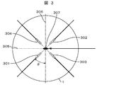
- FIG. 3 is a view of the relationship between the wafer 1 and the first to fourth imaging optical systems 291-294 as viewed from above.
- the first to fourth imaging optical systems 291 to 294 each have an optical fiber array.
- Each optical fiber array has an end for collecting scattered light (hereinafter referred to as a condensing side).
- the first imaging optical system 291 has a first condensing side 301.
- the second imaging optical system 292 has a second condensing side 302.
- the third imaging optical system 293 has a third condensing side 303.
- the fourth imaging optical system 294 has a fourth condensing side 304.
- the first to fourth condensing sides 301 to 304 are arranged so as to surround the illumination spot 307 by the illumination light formed on the wafer 1.
- the first light condensing side 301 is arranged at a certain azimuth angle ⁇ with respect to the wafer 1.
- the third light collecting side 303 is arranged symmetrically with the first light collecting side 301 with respect to an axis 306 orthogonal to the projection line 305 formed by the illumination light on the wafer 1.
- the second light collecting side 302 is arranged symmetrically with the third light collecting side 303 with respect to the projection line 305.
- the fourth light collecting side 304 is arranged symmetrically with the first light collecting side 301 with respect to the projection line 305. Note that the elevation angles of the first to fourth condensing sides 301 to 304 with respect to the wafer are the same. By arranging in this way, defects can be detected efficiently. Moreover, since the light condensed by the optical fiber array is propagated, the photodetector can be arranged at an arbitrary position.
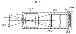
- FIG. 4 is a diagram for explaining the collection and imaging of scattered light.
- the first imaging optical system 291 will be described, but the same applies to the second to fourth imaging optical systems.
- the first imaging optical system 291 includes the first optical fiber array 271a and the first photodetector 270a.
- the first photodetector 270a has an optical sensor array 280 that performs photoelectric conversion.
- the first optical fiber array 271a has a bundle 282 of optical fibers.
- the first optical fiber array 271 a includes a lens 281 for condensing the scattered light from the illumination region 286 onto the first end 283 before the first end 283 of the bundle 282.
- the lens 281 may be a microlens array provided with a lens for each optical fiber of the bundle 282.
- the 1st condensing side mentioned above contains the lens 281 and the 1st edge part 283, for example.
- the optical sensor array 280 has pixels D1-Dn. Pixels D1-Dn are arranged in a straight line.
- Scattered light generated from the illumination area 286 is collected by the lens 281.
- the condensed light is imaged at the first end portion 283.
- the formed image of the illumination area propagates to the second end 284 side and is photoelectrically converted by the photosensor array 280.
- the scattered light from the defect 5 is detected by the pixel D3.
- FIG. 5 is a diagram for explaining the first end 283 and the second end 284.
- the shape of the bundle of optical fibers is a parallelogram having a major axis 501 and a minor axis 502 shorter than the major axis 501 as diagonal lines.
- the shape of the first end portion 283 is not limited to the present embodiment as long as it has two axes having different lengths.
- the shape of the second end portion 284 is a rectangle having a diagonal line 53.
- the relationship between the major axis 501, the minor axis 502, and the diagonal line 503 can be expressed as follows. Short axis 502 ⁇ Diagonal line 503 ⁇ Long axis 501
- the shape of the pixel Dn described above is a rectangle, and light from the optical fibers 510-515 is detected.
- the first end 283 has a folder 6001 for maintaining the shape thereof, and a generally circular folder 6002 for rotating the folder 6001. Further, a cylindrical pin 6003 is arranged in the folder 6002. There is a moving mechanism 6004 having a recess in the vicinity of the pin 6003, and the recess of the moving mechanism 6004 surrounds the pin 6003.
- a ball screw 6005 that moves the moving mechanism 6004 linearly is connected to the moving mechanism 6004.
- a rotating body 6006 (for example, a motor) for rotating the ball screw 6005 is connected to the ball screw 6005. That is, when the rotating body 6006 rotates, the first end portion also rotates. For example, if the rotating body 6006 is a stepping motor, a pulse signal corresponding to the rotation angle of the first end 283 may be given.
- the scattered light from the illumination region is imaged at the first end 283 so as to be approximately the same as the length of the long side 504 of the first end by the lens 281 described above. Is the case. In this case, no correction is necessary.
- FIG. 6B illustrates the case where the scattered light from the illumination region is imaged at the first end 283 longer than the length of the long side 54 of the first end by the lens 281 described above. It is a figure to do.
- the first end 283 is rotated by the angle ⁇ 1 along the long axis 501 described above.
- FIG. 6C illustrates a case where the scattered light from the illumination region is imaged at the first end 283 shorter than the length of the long side 54 of the first end by the lens 281 described above. It is a figure to do.
- the first end 283 is rotated by the angle ⁇ 2 along the short axis 502 described above.
- control related to the correction described above is performed.
- the scattered light from the illumination area can always be correctly imaged on the photodetector.
Landscapes
- Physics & Mathematics (AREA)
- Health & Medical Sciences (AREA)
- Life Sciences & Earth Sciences (AREA)
- Chemical & Material Sciences (AREA)
- Analytical Chemistry (AREA)
- Biochemistry (AREA)
- General Health & Medical Sciences (AREA)
- General Physics & Mathematics (AREA)
- Immunology (AREA)
- Pathology (AREA)
- Investigating Materials By The Use Of Optical Means Adapted For Particular Applications (AREA)
Abstract
検査装置においては検査速度を向上させるためにウェハ表面に細長い光を照明し、照明領域の像を光検出器で結像して、検査を行う方式も考えられる。しかし、光検出器に照明領域の像を正しく結像させるのは容易ではない。従来技術ではこの点に配慮なされていなかった。 本発明は、光ファイバの束を有する結像光学系を有し、さらに前記光ファイバの束の集光側を回転させる機構を有することを特徴とする。本発明によれば、照明領域からの散乱光を正しく光検出器に結像させることができる。
Description
本発明は、基板の傷、異物等の欠陥を検査する検査装置,検査方法に関する。
半導体デバイスの製造工程では、ウェハ表面にパターンを転写し、エッチングで削ることによって回路を形成してゆく。この回路を形成していく様々な半導体デバイスの製造工程において、ウェハ表面の欠陥は、歩留まりを低下させる大きな要因となってくる。
そのため、ウェハ表面の欠陥は、各製造工程において管理され、低減対策が施されている。このウェハ表面に付着している異物やウェハ表面に存在する欠陥などを高感度、及び高スループットで検出するのが、ウェハ表面検査装置である。
ウェハ表面検査装置は、ウェハ表面にレーザ光などの電磁波を照射し、該照射光によって異物・欠陥から生ずる散乱光を検出器で受光することにより、異物の大きさや位置座標データを検出する。検査の高スループット化のため、ウェハが搭載される検査テーブルを高速で回転させながら、検査テーブルが配置されるステージを検査面と同一平面の一軸方向に移動させ、検査用レーザ光を走査させる方式となっている。この表面検査装置は、特許文献1に記載されている。
その他の技術については、特許文献2、及び特許文献3が挙げられる。
検査装置においては検査速度を向上させるためにウェハ表面に細長い光を照明し、照明領域の像を光検出器で結像して、検査を行う方式も考えられる。しかし、光検出器に照明領域の像を正しく結像させるのは容易ではない。従来技術ではこの点に配慮なされていなかった。
本発明は、光ファイバの束を有する結像光学系を有し、さらに前記光ファイバの束の集光側を回転させる機構を有することを特徴とする。
本発明によれば、照明領域からの散乱光を正しく光検出器に結像させることができる。
〔実施例〕
図1は本実施例の表面検査装置の概略構成を示した図である。
図1は本実施例の表面検査装置の概略構成を示した図である。
検査対象であるウェハ1は格納容器であるウェハポッド410に格納されている。
ウェハポッド410は検査装置のロードポート400に配置される。
ウェハ搬送装置300の中にはウェハ搬送ロボット310が配置されている。
ウェハ搬送ロボット310はウェハ1を搬送するためのウェハハンドリングアーム311を有する。
ウェハハンドリングアーム311はウェハポッド410に格納されたウェハ1を取り出し、プリアライメント部320に移動する。
プリアライメント部320では、後述する検査部200で正しく位置決めが行われるように、ウェハ1の中心位置、及びノッチの位置の算出が行われる(プリアライメント)。
プリアライメントが行われたウェハ1は、ウェハハンドリングアーム311によって、検査部200内の検査ステージ210のウェハ保持機構215に移動させられる。
図2は検査部200を詳細に説明する図である。
図1で説明した検査ステージ210は直線移動を行いながら、ウェハ1を高速回転させるものである。検査ステージ210は水平方向に直線移動を行うためのXステージ211、ウェハ1の高さを調節するためのXステージに設けられたZステージ、ウェハ1を高速回転させるためのZステージ211上に設けられたθステージ213によって構成される。なお、θステージ213はスピンドルモータ等の高速回転な回転部を有する。そして、θステージ213上にウェハ保持機構215が配置されている。
上述した検査ステージ210の概略上方には、ウェハ1に光を照明するための光照射部250が配置されている。光照射部250はウェハに対して斜方から線状の光を照明する。
ウェハ1で発生した散乱光は第1の結像光学系291,第2の結像光学系292,後述する第3の結像光学系293,第4の結像光学系294によって、集光,結像,検出される。
第1の結像光学系291は第1の光ファイバアレイ271a、及び第1の光ファイバアレイ271aの結像側に配置された第1の光検出器270aを有する。
第2の結像光学系292は第2の光ファイバアレイ271b、及び第1の光ファイバアレイ271bの結像側に配置された第1の光検出器270bを有する。
ここで、光検出器270a,270bは複数の画素を有するCCD,CMOSセンサー,高速応答が可能なアバランシェフォトダイオード(APD)アレイ、またはマルチピクセルフォトンカウンター等の光電変換器である。
第3の結像光学系293,第4の結像光学系294の構成も同様である。
光検出器270a,270bの検出信号は処理部290において、閾値と比較され閾値を超えた信号は欠陥と判定される。光検出器270a,270bの検出を使って欠陥の分類も行われる。
図3はウェハ1と第1-第4の結像光学系291-294との関係を上方から見た図である。
第1-第4の結像光学系291-294はそれぞれ光ファイバアレイを有する。そしてそれぞれの光ファイバアレイは、散乱光を集光するための端部(以降、集光側と称する)を有する。
第1の結像光学系291は第1の集光側301を有する。第2の結像光学系292は第2の集光側302を有する。第3の結像光学系293は第3の集光側303を有する。第4の結像光学系294は第4の集光側304を有する。
第1-第4の集光側301-304は、ウェハ1上に形成される照明光による照明スポット307を囲むように配置されている。
例えば、第1の集光側301はウェハ1に対してある方位角αで配置されている。第3の集光側303は照明光がウェハ1に形成する投影線305と直交する軸306に対して第1の集光側301と線対称に配置されている。第2の集光側302は投影線305に対して第3の集光側303と線対称に配置されている。第4の集光側304は投影線305に対して第1の集光側301と線対称に配置されている。なお、第1-第4の集光側301-304のウェハに対する仰角は同一である。このように配置することで効率よく欠陥を検出することができる。また、光ファイバアレイで集光した光を伝播するので、光検出器を任意の位置に配置することもできる。
図4は、散乱光の集光,結像を説明する図である。ここでは、第1の結像光学系291について説明するが、第2-第4の結像光学系についても同様である。
第1の結像光学系291は前述したように、第1の光ファイバアレイ271a、及び第1の光検出器270a、を有する。
第1の光検出器270aは光電変換を行う光センサアレイ280を有する。
第1の光ファイバアレイ271aは光ファイバの束282を有する。また、第1の光ファイバアレイ271aは、束282の第1の端部283より前に第1の端部283へ照明領域286からの散乱光を集光するためのレンズ281を有する。ここで、レンズ281は束282の光ファイバ毎にレンズを備えたマイクロレンズアレイであっても良い。
なお、前述した第1の集光側とは例えば、レンズ281と第1の端部283を含むと表現することができる。
光センサアレイ280は画素D1-Dnを有する。画素D1-Dnは直線状に配列されている。
照明領域286から発生した散乱光はレンズ281によって集光される。集光された光は、第1の端部283の部分で結像される。結像された照明領域の像は第2の端部284側に伝播し、光センサアレイ280によって光電変換される。欠陥5からの散乱光は本実施例の場合画素D3で検出されることとなる。
図5は第1の端部283,第2の端部284を説明する図である。
第1の端部283では光ファイバの束の形状は、長軸501と長軸501より短い短軸502とを対角線とする平行四辺形となっている。この2軸を使うことで後述する補正が可能となる。なお、このように長さの異なる2軸を有すれば第1の端部283の形状は本実施例には限定されない。
一方、第2の端部284の形状は、対角線53を有する長方形となっている。ここで、長軸501,短軸502,対角線503の関係は以下のように表現することができる。
短軸502<対角線503<長軸501
短軸502<対角線503<長軸501
また、第1の端部283の長辺504と、第2の端部284の長辺505との関係は、以下のように表現することができる。
長辺504=長辺505
長辺504=長辺505
さらに、前述した画素Dnの形状は長方形であり、光ファイバ510-515からの光を検出する。
このようにすることで、後述する補正を行った場合に、常に照明領域からの散乱光を正しく検出することができる。
次に、図6を用いて光ファイバの束の角度補正について説明する。
第1の端部283はその形状を保つためフォルダ6001、及びフォルダ6001を回転させるための概略円形のフォルダ6002を有する。さらに、フォルダ6002には円柱型のピン6003が配置されている。ピン6003の近傍には凹みを有する移動機構6004があり、移動機構6004の凹みはピン6003を囲っている。そして、移動機構6004には移動機構6004を直線的に移動させるボールネジ6005が接続されている。ボールネジ6005には、ボールネジ6005を回転させるための回転体6006(例えばモータ)が接続されている。即ち、回転体6006が回転することにより第1の端部も回転することになる。例えば、回転体6006がステッピングモータであれば、第1の端部283の回転角に相当するパルス信号を与えてやれば良い。
図6(a)は、前述したレンズ281によって照明領域からの散乱光が第1の端部283において、第1の端部の長辺504の長さと概略同じになるように結像されている場合である。この場合は補正は必要無い。
図6(b)は、前述したレンズ281によって照明領域からの散乱光が第1の端部283において、第1の端部の長辺54の長さより長く結像されてしまっている場合を説明する図である。この場合は、第1の端部283を前述した長軸501に沿うように角度θ1だけ回転させる。
図6(c)は、前述したレンズ281によって照明領域からの散乱光が第1の端部283において、第1の端部の長辺54の長さより短く結像されてしまっている場合を説明する図である。この場合は、第1の端部283を前述した短軸502に沿うように角度θ2だけ回転させる。
本実施例は上述した補正に関する制御を行う。このように補正を行うことで、常に照明領域からの散乱光を正しく光検出器に結像させることができる。
1 ウェハ
200 検査部
210 検査ステージ
270a 第1の光検出器
270b 第2の光検出器
271a 第1の光ファイバアレイ
271b 第2の光ファイバアレイ
280 光センサアレイ
281 レンズ
282 束
283 第1の端部
284 第2の端部
291 第1の結像光学系
292 第2の結像光学系
301 第1の集光側
302 第2の集光側
305 投影線
400 ロードポート
410 ウェハポッド
501 長軸
502 短軸
200 検査部
210 検査ステージ
270a 第1の光検出器
270b 第2の光検出器
271a 第1の光ファイバアレイ
271b 第2の光ファイバアレイ
280 光センサアレイ
281 レンズ
282 束
283 第1の端部
284 第2の端部
291 第1の結像光学系
292 第2の結像光学系
301 第1の集光側
302 第2の集光側
305 投影線
400 ロードポート
410 ウェハポッド
501 長軸
502 短軸
Claims (6)
- 基板を検査する検査装置において、
前記基板に光を照明する照明光学系と、
前記基板からの光を光ファイバの束で集光して結像する検出光学系と、
前記光ファイバの束の集光側を回転させる回転部と、
前記光ファイバの結像側に配置され、前記結像された像を検出する光検出器と、
前記検出器の検出結果を用いて前記基板の欠陥を検出する処理部と、を有することを特徴とする検査装置。 - 請求項1に記載の検査装置おいて、
前記集光側の断面は、平行四辺形であることを特徴とする検査装置。 - 請求項1に記載の検査装置において、
前記結像側の断面は、長方形であることを特徴とする検査装置。 - 請求項1に記載の検査装置において、
前記集光側の形状を保つための第1のフォルダを有することを特徴とする検査装置。 - 請求項1に記載の検査装置において、
前記第1のフォルダを回転させるための第2のフォルダを有することを特徴とする検査装置。 - 請求項1に記載の検査装置おいて、
前記集光側の断面は、長軸、及び前記長軸よりも短い短軸を有する形状であり、
前記結像側の断面は、四角形であり、
前記四角形の対角線は、前記短軸より長く、前記長軸より短いことを特徴とする検査装置。
Priority Applications (1)
| Application Number | Priority Date | Filing Date | Title |
|---|---|---|---|
| US13/994,755 US20130286385A1 (en) | 2010-12-24 | 2011-12-07 | Inspection apparatus |
Applications Claiming Priority (2)
| Application Number | Priority Date | Filing Date | Title |
|---|---|---|---|
| JP2010286917A JP5593213B2 (ja) | 2010-12-24 | 2010-12-24 | 検査装置 |
| JP2010-286917 | 2010-12-24 |
Publications (1)
| Publication Number | Publication Date |
|---|---|
| WO2012086142A1 true WO2012086142A1 (ja) | 2012-06-28 |
Family
ID=46313435
Family Applications (1)
| Application Number | Title | Priority Date | Filing Date |
|---|---|---|---|
| PCT/JP2011/006836 Ceased WO2012086142A1 (ja) | 2010-12-24 | 2011-12-07 | 検査装置 |
Country Status (3)
| Country | Link |
|---|---|
| US (1) | US20130286385A1 (ja) |
| JP (1) | JP5593213B2 (ja) |
| WO (1) | WO2012086142A1 (ja) |
Families Citing this family (2)
| Publication number | Priority date | Publication date | Assignee | Title |
|---|---|---|---|---|
| JP5676419B2 (ja) | 2011-11-24 | 2015-02-25 | 株式会社日立ハイテクノロジーズ | 欠陥検査方法およびその装置 |
| US11143600B2 (en) | 2018-02-16 | 2021-10-12 | Hitachi High-Tech Corporation | Defect inspection device |
Citations (6)
| Publication number | Priority date | Publication date | Assignee | Title |
|---|---|---|---|---|
| JPS60158405A (ja) * | 1984-01-28 | 1985-08-19 | Agency Of Ind Science & Technol | マルチイメ−ジフアイバのためのイメ−ジフアイバ捩れ補正装置 |
| JPH05288999A (ja) * | 1992-04-14 | 1993-11-05 | Hitachi Ltd | ファイバースコープ先端部の保護装置 |
| JPH06174454A (ja) * | 1992-12-03 | 1994-06-24 | Nippon Telegr & Teleph Corp <Ntt> | ホール内検査装置 |
| JPH09139806A (ja) * | 1995-11-16 | 1997-05-27 | Fujikura Ltd | 画像情報読み取り装置 |
| JP2003502634A (ja) * | 1999-06-10 | 2003-01-21 | アプライド マテリアルズ インコーポレイテッド | 可変角度のデザインを用いた光検査の方法及び装置 |
| JP2005160815A (ja) * | 2003-12-03 | 2005-06-23 | Olympus Corp | 光イメージング装置 |
Family Cites Families (5)
| Publication number | Priority date | Publication date | Assignee | Title |
|---|---|---|---|---|
| US5076692A (en) * | 1990-05-31 | 1991-12-31 | Tencor Instruments | Particle detection on a patterned or bare wafer surface |
| US5363187A (en) * | 1990-09-12 | 1994-11-08 | Nikon Corporation | Light scanning apparatus for detecting foreign particles on surface having circuit pattern |
| JPH0643111A (ja) * | 1992-04-20 | 1994-02-18 | Nikon Corp | 欠陥検査装置 |
| US5798831A (en) * | 1991-12-19 | 1998-08-25 | Nikon Corporation | Defect inspecting apparatus and defect inspecting method |
| US7061598B1 (en) * | 2002-09-27 | 2006-06-13 | Kla-Tencor Technologies Corporation | Darkfield inspection system having photodetector array |
-
2010
- 2010-12-24 JP JP2010286917A patent/JP5593213B2/ja not_active Expired - Fee Related
-
2011
- 2011-12-07 WO PCT/JP2011/006836 patent/WO2012086142A1/ja not_active Ceased
- 2011-12-07 US US13/994,755 patent/US20130286385A1/en not_active Abandoned
Patent Citations (6)
| Publication number | Priority date | Publication date | Assignee | Title |
|---|---|---|---|---|
| JPS60158405A (ja) * | 1984-01-28 | 1985-08-19 | Agency Of Ind Science & Technol | マルチイメ−ジフアイバのためのイメ−ジフアイバ捩れ補正装置 |
| JPH05288999A (ja) * | 1992-04-14 | 1993-11-05 | Hitachi Ltd | ファイバースコープ先端部の保護装置 |
| JPH06174454A (ja) * | 1992-12-03 | 1994-06-24 | Nippon Telegr & Teleph Corp <Ntt> | ホール内検査装置 |
| JPH09139806A (ja) * | 1995-11-16 | 1997-05-27 | Fujikura Ltd | 画像情報読み取り装置 |
| JP2003502634A (ja) * | 1999-06-10 | 2003-01-21 | アプライド マテリアルズ インコーポレイテッド | 可変角度のデザインを用いた光検査の方法及び装置 |
| JP2005160815A (ja) * | 2003-12-03 | 2005-06-23 | Olympus Corp | 光イメージング装置 |
Also Published As
| Publication number | Publication date |
|---|---|
| US20130286385A1 (en) | 2013-10-31 |
| JP2012132859A (ja) | 2012-07-12 |
| JP5593213B2 (ja) | 2014-09-17 |
Similar Documents
| Publication | Publication Date | Title |
|---|---|---|
| JP7373527B2 (ja) | ワークピースの欠陥検出装置及び方法 | |
| TWI793578B (zh) | 用於晶圓檢測之系統 | |
| US7847927B2 (en) | Defect inspection method and defect inspection apparatus | |
| TW516083B (en) | Optical sensor | |
| US20140118730A1 (en) | Sample Inspection System Detector | |
| JP5918009B2 (ja) | 欠陥検査方法および欠陥検査装置 | |
| JP5405956B2 (ja) | 欠陥検査装置 | |
| US9568437B2 (en) | Inspection device | |
| JP5349742B2 (ja) | 表面検査方法及び表面検査装置 | |
| WO2025049065A1 (en) | Multidirectional illumination for hybrid bonding defect detection | |
| US12366538B2 (en) | Defect inspection apparatus and defect inspection method | |
| JP5593213B2 (ja) | 検査装置 | |
| KR102160025B1 (ko) | 하전 입자빔 장치 및 광학식 검사 장치 | |
| JP5927010B2 (ja) | 検査装置 | |
| JP5877679B2 (ja) | レチクルの支持機構および検査装置 | |
| KR20260057334A (ko) | 하이브리드 접합 결함 검출을 위한 다방향 조명 | |
| JPH1183755A (ja) | 傷検査装置 | |
| JP2009276207A (ja) | 表面欠陥検査装置 | |
| JP2021167794A (ja) | 欠陥検査装置、欠陥検査方法、散乱光検出系 | |
| JPH06123708A (ja) | 異物検査装置 |
Legal Events
| Date | Code | Title | Description |
|---|---|---|---|
| 121 | Ep: the epo has been informed by wipo that ep was designated in this application |
Ref document number: 11850645 Country of ref document: EP Kind code of ref document: A1 |
|
| WWE | Wipo information: entry into national phase |
Ref document number: 13994755 Country of ref document: US |
|
| NENP | Non-entry into the national phase |
Ref country code: DE |
|
| 122 | Ep: pct application non-entry in european phase |
Ref document number: 11850645 Country of ref document: EP Kind code of ref document: A1 |