WO2012073777A1 - 電子機器用銅合金、電子機器用銅合金の製造方法及び電子機器用銅合金圧延材 - Google Patents
電子機器用銅合金、電子機器用銅合金の製造方法及び電子機器用銅合金圧延材 Download PDFInfo
- Publication number
- WO2012073777A1 WO2012073777A1 PCT/JP2011/077011 JP2011077011W WO2012073777A1 WO 2012073777 A1 WO2012073777 A1 WO 2012073777A1 JP 2011077011 W JP2011077011 W JP 2011077011W WO 2012073777 A1 WO2012073777 A1 WO 2012073777A1
- Authority
- WO
- WIPO (PCT)
- Prior art keywords
- copper alloy
- atomic
- less
- electronic devices
- copper
- Prior art date
- Legal status (The legal status is an assumption and is not a legal conclusion. Google has not performed a legal analysis and makes no representation as to the accuracy of the status listed.)
- Ceased
Links
Images


Classifications
-
- H—ELECTRICITY
- H01—ELECTRIC ELEMENTS
- H01B—CABLES; CONDUCTORS; INSULATORS; SELECTION OF MATERIALS FOR THEIR CONDUCTIVE, INSULATING OR DIELECTRIC PROPERTIES
- H01B1/00—Conductors or conductive bodies characterised by the conductive materials; Selection of materials as conductors
- H01B1/02—Conductors or conductive bodies characterised by the conductive materials; Selection of materials as conductors mainly consisting of metals or alloys
- H01B1/026—Alloys based on copper
-
- C—CHEMISTRY; METALLURGY
- C22—METALLURGY; FERROUS OR NON-FERROUS ALLOYS; TREATMENT OF ALLOYS OR NON-FERROUS METALS
- C22C—ALLOYS
- C22C9/00—Alloys based on copper
- C22C9/01—Alloys based on copper with aluminium as the next major constituent
-
- C—CHEMISTRY; METALLURGY
- C22—METALLURGY; FERROUS OR NON-FERROUS ALLOYS; TREATMENT OF ALLOYS OR NON-FERROUS METALS
- C22F—CHANGING THE PHYSICAL STRUCTURE OF NON-FERROUS METALS AND NON-FERROUS ALLOYS
- C22F1/00—Changing the physical structure of non-ferrous metals or alloys by heat treatment or by hot or cold working
- C22F1/08—Changing the physical structure of non-ferrous metals or alloys by heat treatment or by hot or cold working of copper or alloys based thereon
-
- H—ELECTRICITY
- H01—ELECTRIC ELEMENTS
- H01B—CABLES; CONDUCTORS; INSULATORS; SELECTION OF MATERIALS FOR THEIR CONDUCTIVE, INSULATING OR DIELECTRIC PROPERTIES
- H01B13/00—Apparatus or processes specially adapted for manufacturing conductors or cables
- H01B13/0016—Apparatus or processes specially adapted for manufacturing conductors or cables for heat treatment
Definitions
- the present invention relates to a copper alloy for electronic equipment suitable for electronic electrical components such as terminals, connectors and relays, a method for producing a copper alloy for electronic equipment, and a rolled copper alloy material for electronic equipment.
- Patent Document 1 provides a Cu—Be alloy containing Be.
- the strength is improved without lowering the conductivity by aging precipitation of CuBe in the matrix, and this Cu—Be alloy is a precipitation hardening type high strength alloy.
- Patent Document 2 provides a Cu—Ni—Si alloy (so-called Corson alloy).
- Corson alloy is a precipitation hardening type alloy in which Ni 2 Si precipitates are dispersed, and has relatively high electrical conductivity, strength, and stress relaxation characteristics. For this reason, Corson alloys are widely used in applications such as automobile terminals and signal system small terminals, and have been actively developed in recent years.
- a Cu—Mg—P alloy described in Patent Document 3 has been developed.
- the Corson alloy disclosed in Patent Document 2 generally has a relatively high Young's modulus of 126 to 135 GPa.
- the connector having a structure in which the male tab is inserted by pushing up the spring contact portion of the female terminal when the Young's modulus of the material constituting the connector is high, the contact pressure fluctuation at the time of insertion is severe. Furthermore, there is a risk of plastic deformation easily exceeding the elastic limit. For this reason, a material with a high Young's modulus is not preferable for the connector.
- the Cu—Mg—P alloy described in Patent Document 3 has high electrical conductivity, but has insufficient mechanical properties such as proof stress and tensile strength. Further, since the Young's modulus is relatively high, there is a problem that it is not suitable for a connector.
- This invention has been made in view of the circumstances described above, and has a low Young's modulus, high proof stress, and high conductivity, and is suitable for electronic electrical components such as terminals, connectors and relays, It aims at providing the manufacturing method of the copper alloy for electronic devices, and the copper alloy rolling material for electronic devices.
- Mg is included in the range of 1.3 atomic% or more and less than 2.6 atomic%
- Al is included in the range of 6.7 atomic% or more and 20 atomic% or less
- the balance is substantially Cu and inevitable impurities.
- a copper alloy for electronic equipment characterized in that there is.
- a processing step of processing the rapidly cooled copper material wherein the copper material contains Mg in a range of 1.3 atomic% or more and less than 2.6 atomic%, and Al is 6.7 atomic% or more 20
- the copper alloy constituting the copper material further includes one or more selected from Zn, Sn, Si, Mn, and Ni, and the content thereof is 0.05 atomic% or more and 5 atomic% or less.
- the copper alloy constituting the copper material further contains one or more selected from B, P, Zr, Fe, Co, Cr, Ag, Ca, and a rare earth element, and the content thereof is 0.00.
- the copper alloy rolled material for electronic equipment according to [10] which is used as a terminal, a connector, or a relay.
- One aspect of the copper alloy for electronic devices of the present invention includes Mg in a range of 1.3 atomic% or more and less than 2.6 atomic%, and Al in a range of 6.7 atomic% or more and 20 atomic% or less, The balance is substantially Cu and inevitable impurities.
- This copper alloy for electronic equipment contains Mg and Al, and the balance is substantially Cu and inevitable impurities, and the Mg content and the Al content are specified as described above.
- a copper alloy having such a component composition has characteristics of low Young's modulus and high strength, and has a relatively high electrical conductivity.
- the above-described copper alloy for electronic devices further includes one or more selected from Zn, Sn, Si, Mn, and Ni, and the content thereof is preferably 0.05 atomic percent or more and 5 atomic percent or less. .
- the characteristics of the copper alloy can be improved.
- the copper alloy for electronic devices especially suitable for the use can be provided by making the said element contain selectively according to a use.
- the above-described copper alloy for electronic devices further includes one or more selected from B, P, Zr, Fe, Co, Cr, Ag, Ca, and rare earth elements, and the content thereof is 0.01 atomic% or more. It is preferable that it is 1 atomic% or less.
- the characteristics of the copper alloy are improved. It becomes possible. For this reason, the copper alloy for electronic devices especially suitable for the use can be provided by making the said element contain selectively according to a use.
- the 0.2% yield strength ⁇ 0.2 is 400 MPa or more.
- the Young's modulus E is preferably 125 GPa or less.
- the 0.2% proof stress ⁇ 0.2 is 400 MPa or more, or the Young's modulus E is 125 GPa or less, the elastic energy coefficient ( ⁇ 0.2 2 / 2E) increases, and plastic deformation does not easily occur.
- the copper alloy for electronic devices is particularly suitable for electronic and electrical parts such as terminals, connectors, and relays.
- the average number of intermetallic compounds having a particle diameter of 0.1 ⁇ m or more observed with a scanning electron microscope is preferably 10 / ⁇ m 2 or less.
- the average number of intermetallic compounds having a particle size of 0.1 ⁇ m or more observed with a scanning electron microscope is 10 / ⁇ m 2 or less.
- precipitation of coarse intermetallic compounds is suppressed, and Mg And at least a part of Al is in a state of being dissolved in the matrix.
- the strength and recrystallization temperature can be increased while maintaining high conductivity, and the Young's modulus can be decreased. Can do.
- the average number of coarse intermetallic compounds having a particle size of 0.1 ⁇ m or more was observed using a field emission scanning electron microscope at 10 magnifications with a magnification of 50,000 times and a visual field of about 4.8 ⁇ m 2. Go and calculate.
- the particle size of the intermetallic compound is the average value of the major axis and minor axis of the intermetallic compound.
- the major axis is the length of a straight line that can be drawn the longest in the grain under conditions that do not contact the grain boundary in the middle
- the minor axis is a direction that intersects the major axis at a right angle and does not contact the grain boundary in the middle. This is the length of the straight line that can be drawn the longest.
- One aspect of the method for producing a copper alloy for electronic equipment according to the present invention is a method for producing one aspect of the above-described copper alloy for electronic equipment.
- One aspect of the method for producing a copper alloy for electronic equipment is a heating step of heating a copper material to a temperature of 500 ° C. or more and 1000 ° C. or less, and the heated copper material at a cooling rate of 200 ° C./min or more.
- the copper material includes Mg in a range of 1.3 atomic% or more and less than 2.6 atomic%, and It is made of a copper alloy containing Al in a range of 6.7 atomic% to 20 atomic% with the balance being substantially Cu and inevitable impurities.
- a solution of Mg and Al is formed by a heating step of heating a copper material containing Mg and Al having the above composition to a temperature of 500 ° C. or higher and 1000 ° C. or lower. It can be performed.
- the heating temperature is less than 500 ° C.
- solutionization is incomplete, and a large amount of coarse intermetallic compounds may remain in the matrix phase.
- the heating temperature exceeds 1000 ° C., a part of the copper material becomes a liquid phase, and the structure and the surface state may become non-uniform. For this reason, heating temperature is set to the range of 500 degreeC or more and 1000 degrees C or less.
- the processing method is not particularly limited.
- the final form is a plate or a strip
- rolling is employed.
- the final form is a wire or bar
- wire drawing or extrusion is employed.
- the final form is a bulk shape, forging or pressing is adopted.
- the processing temperature is not particularly limited, but is preferably adjusted to a range of ⁇ 200 ° C. to 200 ° C., which is cold or warm processing, so that precipitation does not occur.
- the processing rate is appropriately selected so as to be close to the final shape, but is preferably 20% or more, and more preferably 30% or more in consideration of work hardening.
- the processing rate is a value obtained by dividing the difference between the cross-sectional area of the material before processing and the cross-sectional area after processing by the cross-sectional area before processing to calculate a ratio, and expressing this ratio as a percentage.
- so-called low-temperature annealing may be performed after the processing step. This low-temperature annealing can further improve the mechanical properties.
- the copper alloy constituting the copper material further includes one or more selected from Zn, Sn, Si, Mn, and Ni, and the content thereof is 0.00. It may be from 05 atomic% to 5 atomic%.
- the copper alloy constituting the copper material further includes one or more selected from B, P, Zr, Fe, Co, Cr, Ag, Ca, and rare earth elements, and the content thereof is 0.01 atomic%. It may be 1 atomic% or less.
- One aspect of the copper alloy rolled material for electronic equipment according to the present invention comprises one aspect of the above-described copper alloy for electronic equipment.
- the Young's modulus E in the rolling direction is 125 GPa or less and the 0.2% proof stress ⁇ 0.2 in the rolling direction. Is 400 MPa.
- the elastic energy coefficient ( ⁇ 0.2 2 / 2E) is high, and plastic deformation does not easily occur. It is preferable that the one aspect
- a copper alloy for electronic equipment having a low Young's modulus, high proof stress, and high conductivity and suitable for electronic electrical parts such as terminals, connectors and relays, a method for producing a copper alloy for electronic equipment, and A rolled copper alloy material for electronic equipment can be provided.
- the copper alloy for electronic devices which is one Embodiment of this invention is demonstrated.
- the copper alloy for electronic devices according to the present embodiment includes Mg in a range of 1.3 atomic% to less than 2.6 atomic%, Al in a range of 6.7 atomic% to 20 atomic%, Containing one or more selected from Zn, Sn, Si, Mn, and Ni in a content of 0.05 atomic% or more and 5 atomic% or less, and containing B, P, Zr, Fe, Co, Cr, Ag, Ca, And one or more selected from rare earth elements in a content of 0.01 atomic% or more and 1 atomic% or less, with the balance being composed of Cu and inevitable impurities.
- the average number of the intermetallic compounds with a particle size of 0.1 micrometer or more observed with a scanning electron microscope is 10 pieces / micrometer ⁇ 2 > or less. The reason why the contents of these elements are set in the above-described range will be described below.
- Mg Mg is an element that has the effect of improving the strength and raising the recrystallization temperature without greatly reducing the electrical conductivity.
- the Young's modulus can be kept low by dissolving Mg in the matrix.
- the Mg content is less than 1.3 atomic%, the effect cannot be obtained.
- the Mg content is 2.6 atomic% or more, if the material temperature during hot working is 800 ° C. or more, a liquid phase may partially form and cracks may occur. For this reason, the material temperature at the time of hot processing cannot be set high, and production efficiency will fall. For these reasons, the Mg content is set to 1.3 atomic% or more and less than 2.6 atomic%.
- Al Al is an element having an effect of greatly improving the strength without increasing the Young's modulus by being dissolved in a copper alloy in which a part or all of Mg is dissolved.
- the Al content is less than 6.7 atomic%, the effect cannot be obtained.
- the Al content exceeds 20 atomic%, a large amount of intermetallic compounds remain when heat treatment is performed for solution treatment, and cracks may occur during subsequent processing. .
- the Al content is set to 6.7 atomic% or more and 20 atomic% or less.
- Zn, Sn, Si, Mn, Ni Elements such as Zn, Sn, Si, Mn, Ni have an effect of improving the characteristics of the copper alloy by adding to a copper alloy in which a part or all of Mg and Al are dissolved. For this reason, it becomes possible to improve a characteristic by making it contain selectively according to a use.
- Zn has the effect of improving the strength without reducing the electrical conductivity.
- the content of one or more elements selected from Zn, Sn, Si, Mn, and Ni is less than 0.05 atomic%, the effect cannot be obtained.
- the content of one or more elements selected from Zn, Sn, Si, Mn, and Ni exceeds 5 atomic%, the conductivity is greatly reduced.
- the content of one or more elements selected from Zn, Sn, Si, Mn, and Ni is set to 0.05 atomic% or more and 5 atomic% or less.
- the content means the total amount of 2 or more types of elements.
- the rare earth element is one or more elements selected from Sc, Y, La, Ce, Pr, Nd, Pm, Sm, Eu, Gd, Tb, Dy, Ho, Er, Tm, Yb, and Lu. is there.
- the content of one or more elements selected from B, P, Zr, Fe, Co, Cr, Ag, Ca, and rare earth elements is less than 0.01 atomic%, the effect cannot be obtained. .
- the content of one or more elements selected from B, P, Zr, Fe, Co, Cr, Ag, Ca, and rare earth elements exceeds 1 atomic%, the conductivity is greatly reduced. become. Further, when heat treatment is performed for solution treatment, a large amount of coarse compounds may remain. For these reasons, the content of one or more elements selected from B, P, Zr, Fe, Co, Cr, Ag, Ca, and rare earth elements is 0.01 atomic% or more and 1 atomic% or less. It is set. In addition, when containing 2 or more types of said elements, the content means the total amount of 2 or more types of elements.
- Inevitable impurities include Sr, Ba, Hf, V, Nb, Ta, Mo, W, Re, Ru, Os, Se, Te, Rh, Ir, Pd, Pt, Au, Cd, Ga, In, Li, Ge. , As, Sb, Ti, Tl, Pb, Bi, S, O, C, Be, N, H, Hg, and the like. These inevitable impurities are desirably 0.3% by mass or less in total.
- the average number of intermetallic compounds having a particle size of 0.1 ⁇ m or more is 10 / ⁇ m 2 or less. That is, many coarse intermetallic compounds are not precipitated, and at least a part of Mg and Al is dissolved in the matrix.
- these intermetallic compounds become the starting point of cracking. For this reason, cracks occur during processing, and bending workability is greatly deteriorated. Further, if the amount of the intermetallic compound is large, the Young's modulus increases, which is not preferable.
- the number of coarse intermetallic compounds having a particle size of 0.1 ⁇ m or more is 10 / ⁇ m 2 or less in the alloy, that is, when there are no coarse intermetallic compounds or a small amount Good bending workability and low Young's modulus can be obtained. Furthermore, in order to reliably obtain the above-described effects, it is preferable that the number of intermetallic compounds having a particle size of 0.1 ⁇ m or more is 1 / ⁇ m 2 or less in the alloy. Furthermore, when bending workability is strongly required, the number of intermetallic compounds having a particle size of 0.05 ⁇ m or more is more preferably 1 / ⁇ m 2 or less in the alloy.
- the average number of intermetallic compounds was determined by observing 10 fields of view using a field emission scanning electron microscope at a magnification of 50,000 times and a field of view of about 4.8 ⁇ m 2 . The average value of the number is calculated.
- the particle size of the intermetallic compound is the average value of the major axis and minor axis of the intermetallic compound.
- the major axis is the length of a straight line that can be drawn the longest in the grain under conditions that do not contact the grain boundary in the middle
- the minor axis is a direction that intersects the major axis at a right angle and does not contact the grain boundary in the middle. This is the length of the straight line that can be drawn the longest.
- the manufacturing method of the copper alloy for electronic devices which is this embodiment is demonstrated with reference to the flowchart shown in FIG. (Melting / Casting Process S01)
- the above-mentioned elements are added to a molten copper obtained by melting a copper raw material, and the components are adjusted to produce a molten copper alloy.
- elements such as Mg and Al
- elemental elements such as Mg and Al, mother alloys, and the like can be used.
- the molten copper is preferably made of copper (so-called 4NCu) having a purity of 99.99% by mass or more.
- the melting step it is preferable to use a vacuum furnace or an atmosphere furnace in which an inert gas atmosphere or a reducing atmosphere is used in order to suppress oxidation of elements such as Mg and Al.
- the ingot is manufactured by inject
- This ingot is a copper material made of a copper alloy.
- mass production it is preferable to use a continuous casting method or a semi-continuous casting method.
- Heating step S02 Next, heat treatment is performed for homogenization and solution of the obtained ingot.
- intermetallic compounds and the like are generated and present due to segregation and concentration of additive elements during the solidification process. Therefore, in order to eliminate or reduce these segregation and intermetallic compounds, the ingot is heated to a temperature of 500 ° C. or higher and 1000 ° C. or lower (heat treatment), thereby uniformly diffusing additive elements in the ingot. Or the additive element is dissolved in the matrix.
- this heating process S02 in a non-oxidizing atmosphere or a reducing atmosphere.
- Rapid cooling step S03 the ingot heated to 500 ° C. or higher and 1000 ° C. or lower in the heating step S02 is cooled to a temperature of 200 ° C. or lower at a cooling rate of 200 ° C./min or higher.
- this rapid cooling step S03 it is suppressed that Mg and Al dissolved in the matrix phase are precipitated as intermetallic compounds.
- the average number of intermetallic compounds having a particle size of 0.1 ⁇ m or more observed with a scanning electron microscope is 10 / ⁇ m 2 or less.
- the processing method is not particularly limited.
- rolling can be employed.
- the final form is a wire or bar, drawing, extrusion, groove rolling, or the like can be employed.
- the heating step S02 and the rapid cooling step S03 may be performed again for the purpose of reliably performing solution treatment. That is, the heating step S02 and the rapid cooling step S03 may be repeatedly performed to achieve homogenization and solution.
- Processing step S04 The ingot which passed through heating process S02 and rapid cooling process S03 is cut
- the processing method is not particularly limited. For example, when the final form is a plate or a strip, rolling can be employed. When the final form is a wire or bar, wire drawing, extrusion, and groove rolling can be employed. When the final form is a bulk shape, forging or pressing can be employed.
- the temperature condition in this processing step S04 is not particularly limited, but it is preferable to set the processing temperature within a range of ⁇ 200 ° C. to 200 ° C. so that cold processing or warm processing is performed. Further, the processing rate is appropriately selected so as to approximate the final shape. In order to improve the strength by work hardening, the working rate is preferably 20% or more. Also. In order to further improve the strength, the processing rate is more preferably 30% or more. Furthermore, the above heating step S02, quenching step S03, and processing step S04 may be repeated. Here, the second and subsequent heating steps S02 are intended for thorough solutionization, recrystallization texture formation, or softening for improving workability. Moreover, it is not an ingot but a processed material.
- Heat treatment step S05 Next, a heat treatment is performed on the processed material obtained in the processing step S04 in order to perform low-temperature annealing hardening or to remove residual strain.
- the conditions for this heat treatment are appropriately set according to the characteristics required for the manufactured product.
- heat treatment conditions temperature, time, cooling rate
- the cooling rate is preferably 200 ° C./min or more.
- the heat treatment method is not particularly limited, but the heat treatment at 100 to 500 ° C. for 0.1 second to 24 hours is preferably performed in a non-oxidizing or reducing atmosphere.
- the cooling method is not particularly limited, but a method such as water quenching that allows the cooling rate to be 200 ° C./min or more is preferable. Further, the above-described processing step S04 and heat treatment step S05 may be repeatedly performed.
- the copper alloy for electronic devices which is this embodiment is manufactured.
- the copper alloy for electronic devices which is this embodiment has Young's modulus E of 125 GPa or less, and 0.2% yield strength ⁇ 0.2 is 400 MPa or more.
- the rolled copper alloy material for electronic devices of the present embodiment is made of the above-described copper alloy for electronic devices of the present embodiment, has a Young's modulus E in the rolling direction of 125 GPa or less, and 0.2% proof stress ⁇ 0. 2 is 400 MPa or more.
- the rolled copper alloy material for electronic equipment is produced by rolling in the processing step S04 of the above-described method for producing a copper alloy for electronic equipment.
- Mg is included in the range of 1.3 atomic% or more and less than 2.6 atomic%, and Al is 6. It is included in the range of 7 atomic% to 20 atomic%.
- a copper alloy having such a component composition has a low Young's modulus, a high strength, and a relatively high electrical conductivity. Specifically, the Young's modulus E is 125 GPa or less, and the 0.2% proof stress ⁇ 0.2 is 400 MPa or more.
- the copper alloy for electronic equipment and the copper alloy rolled material for electronic equipment are electronic devices such as terminals, connectors, and relays. Particularly suitable for electrical components.
- 1 or more types selected from Zn, Sn, Si, Mn, and Ni are further included, and the content is 0.05 atomic% or more and 5 atomic% or less.
- 1 or more types selected from B, P, Zr, Fe, Co, Cr, Ag, Ca, and rare earth elements are included, and the content is 0.01 atomic% or more and 1 atomic% or less.
- One or more elements selected from Zn, Sn, Si, Mn, and Ni, and one or more elements selected from B, P, Zr, Fe, Co, Cr, Ag, Ca, and rare earth elements are By adding to a copper alloy in which Mg and Al are dissolved, the effect of improving the characteristics of the copper alloy is obtained. Therefore, the copper alloy for electronic devices and the copper alloy rolled material for electronic devices which are particularly suitable for the use can be provided by selectively containing it according to the use.
- the average number of intermetallic compounds having a particle diameter of 0.1 ⁇ m or more observed with a scanning electron microscope is 10 / ⁇ m 2. It is as follows. Thus, since the average number of intermetallic compounds having a particle size of 0.1 ⁇ m or more is defined, precipitation of coarse intermetallic compounds is suppressed, and at least a part of Mg and Al is dissolved in the matrix. It is in a state. For this reason, the strength and the recrystallization temperature can be increased while maintaining high electrical conductivity. Furthermore, the Young's modulus can be lowered. Also, good bending workability can be obtained.
- the heating process S02 which heats to the temperature of 500 to 1000 degreeC with respect to the ingot or processed material of the above-mentioned composition is provided.
- solution treatment of Mg and Al can be performed by this heating process S02.
- the rapid cooling process S03 which cools the ingot or processed material heated to 500 to 1000 degreeC by heating process S02 to 200 degrees C or less with the cooling rate of 200 degrees C / min or more is provided. For this reason, it can suppress that a large size intermetallic compound precipitates in the process of cooling.
- the processing step S04 for processing the quenched material since the processing step S04 for processing the quenched material is provided, the strength can be improved by work hardening.
- a heat treatment step S05 is performed in order to perform low-temperature annealing hardening or to remove residual strain. For this reason, it is possible to further improve the mechanical characteristics.
- the copper alloy for electronic equipment having low Young's modulus, high yield strength, high conductivity, and excellent bending workability, and suitable for electronic and electrical parts such as terminals, connectors, and relays.
- the copper alloy rolling material for electronic devices can be provided.
- the present invention is not limited thereto, and is appropriately changed without departing from the scope of the claims. Is possible.
- a method for manufacturing a copper alloy for electronic devices has been described.
- the manufacturing method is not limited to this embodiment, and an existing manufacturing method may be selected as appropriate. Good.
- a copper raw material made of oxygen-free copper (ASTM B152 C10100) having a purity of 99.99% by mass or more was prepared.
- the copper raw material was charged into a high-purity graphite crucible and melted at a high frequency in an atmosphere furnace having an Ar gas atmosphere to obtain a molten copper.
- Various additive elements were added to the obtained molten copper to prepare the component compositions shown in Tables 1 and 2 to obtain a molten copper alloy.
- An ingot was manufactured by pouring molten copper alloy into a carbon mold. The size of the ingot was about 20 mm thick x about 20 mm wide x about 100 to 120 mm long.
- the balance of the component composition shown in Tables 1 and 2 is copper and inevitable impurities.
- the ingot was held at 820 ° C. for 4 hours in an Ar gas atmosphere, and then water quenching was performed.
- hot rolling is performed by adjusting the maximum value of the material temperature during hot rolling to be in the range of 800 to 820 ° C., and then water quenching is performed to obtain a heat of 10 mm thickness ⁇ width about 20 mm.
- a rolled material was produced.
- the electrical conductivity and mechanical properties were measured using the above-described strips for property evaluation.
- (conductivity) A test piece having a width of 10 mm and a length of 60 mm was taken from the strip for characteristic evaluation. This test piece was sampled so that its longitudinal direction was parallel to the rolling direction of the strip for property evaluation. The electrical resistance of the test piece was determined by the 4-terminal method. Moreover, the dimension of the test piece was measured using the micrometer, and the volume of the test piece was calculated. And electrical conductivity was computed from the measured electrical resistance value and volume.
- the average value of the major axis and minor axis of the intermetallic compound was taken as the particle size of the intermetallic compound.
- the major axis of the intermetallic compound is the length of the straight line that can be drawn the longest in the grain under the condition that it does not touch the grain boundary in the middle. This is the length of the straight line that can be drawn the longest under the conditions. Then, the density of intermetallic compounds having a particle size of 0.1 ⁇ m or more (pieces / ⁇ m 2 ) and the density of intermetallic compounds having 0.05 ⁇ m or more (pieces / ⁇ m 2 ) were determined.
- Tables 1 and 2 show manufacturing conditions and evaluation results. Further, as an example of the above-described structure observation, an SEM observation photograph of Example 6 of the present invention is shown in FIG.
- Comparative Examples 1 and 2 in which the Mg content and the Al content are less than the range defined in the present embodiment, the Young's modulus is relatively high as 126 GPa and 126 GPa, and the 0.2% proof stress is 520 MPa and 340 MPa. And showed a low value. Therefore, in Comparative Examples 1 and 2, the elastic energy coefficient ( ⁇ 0.2 2 / 2E) is low, and plastic deformation is likely to occur. For this reason, it is judged that it is unsuitable for electronic electrical parts, such as a terminal, a connector, and a relay.
- Comparative Example 3 in which the Al content is larger than the range defined in the present embodiment, large ear cracks occurred during cold rolling, and it was impossible to perform subsequent characteristic evaluation.
- Comparative Example 4 in which the Mg content is larger than the range defined in the present embodiment, cracks occurred during hot rolling, and it was impossible to perform subsequent characteristic evaluation.
- the copper alloy for electronic devices and the rolled copper alloy material for electronic devices of the present embodiment have a low Young's modulus, a high yield strength, and a high conductivity. For this reason, it is suitably applied to electronic and electrical parts such as terminals, connectors, and relays.
Landscapes
- Chemical & Material Sciences (AREA)
- Engineering & Computer Science (AREA)
- Materials Engineering (AREA)
- Mechanical Engineering (AREA)
- Metallurgy (AREA)
- Organic Chemistry (AREA)
- Physics & Mathematics (AREA)
- Thermal Sciences (AREA)
- Crystallography & Structural Chemistry (AREA)
- Manufacturing & Machinery (AREA)
- Conductive Materials (AREA)
Abstract
この電子機器用銅合金は、Mg:1.3原子%以上2.6原子%未満、及びAl:6.7原子%以上20原子%以下を含み、残部が実質的にCu及び不可避不純物である。この電子機器用銅合金の製造方法は、銅素材を500℃以上1000℃以下の温度にまで加熱する加熱工程と、加熱された前記銅素材を、200℃/min以上の冷却速度で、200℃以下の温度まで冷却する急冷工程と、急冷された前記銅素材を加工する加工工程を備え、前記銅素材は、Mg:1.3原子%以上2.6原子%未満、及びAl:6.7原子%以上20原子%以下を含み、残部が実質的にCu及び不可避不純物である銅合金からなる。この電子機器用銅合金圧延材は、前記電子機器用銅合金からなり、圧延方向のヤング率Eが125GPa以下、圧延方向の0.2%耐力σ0.2が400MPa以上である。
Description
本発明は、例えば端子、コネクタやリレー等の電子電気部品に適した電子機器用銅合金、電子機器用銅合金の製造方法及び電子機器用銅合金圧延材に関する。
本願は、2010年12月3日に、日本に出願された特願2010-270890号に基づき優先権を主張し、その内容をここに援用する。
本願は、2010年12月3日に、日本に出願された特願2010-270890号に基づき優先権を主張し、その内容をここに援用する。
従来、電子機器や電気機器などの小型化にともない、これら電子機器や電気機器などに使用される端子、コネクタやリレーなどの電子電気部品の小型化及び薄肉化が図られている。このため、電子電気部品を構成する材料として、ばね性、強度、導電率の優れた銅合金が要求されている。特に、非特許文献1に記載されているように、端子、コネクタやリレー等の電子電気部品として使用される銅合金としては、耐力が高く、かつヤング率が低いものが望ましい。
そこで、ばね性、強度、導電率の優れた銅合金として、例えば特許文献1には、Beを含有したCu-Be合金が提供されている。特許文献1では、母相中にCuBeを時効析出させることによって、導電率を低下させることなく強度を向上させており、このCu-Be合金は析出硬化型の高強度合金である。
そこで、ばね性、強度、導電率の優れた銅合金として、例えば特許文献1には、Beを含有したCu-Be合金が提供されている。特許文献1では、母相中にCuBeを時効析出させることによって、導電率を低下させることなく強度を向上させており、このCu-Be合金は析出硬化型の高強度合金である。
しかしながら、このCu-Be合金は、高価な元素であるBeを含有しているため、原料コストが非常に高い。また、Cu-Be合金を製造する際には、毒性のあるBe酸化物が発生することになる。このため、製造工程において、Be酸化物が誤って外部に放出されないように、製造設備を特別な構成とし、Be酸化物を厳しく管理する必要がある。
このように、Cu-Be合金は、原料コスト及び製造コストがともに高く、非常に高価であるといった問題があった。また、前述のように、有害な元素であるBeを含有していることから、環境対策の面からも敬遠されていた。
そこで、Cu-Be合金を代替可能な材料が強く望まれていた。
このように、Cu-Be合金は、原料コスト及び製造コストがともに高く、非常に高価であるといった問題があった。また、前述のように、有害な元素であるBeを含有していることから、環境対策の面からも敬遠されていた。
そこで、Cu-Be合金を代替可能な材料が強く望まれていた。
Cu-Be合金を代替可能な材料として、例えば特許文献2には、Cu-Ni-Si系合金(いわゆるコルソン合金)が提供されている。このコルソン合金は、Ni2Si析出物が分散された析出硬化型合金であり、比較的高い導電率と強度、応力緩和特性を有する。このため、コルソン合金は、自動車用端子や信号系小型端子などの用途に多用されており、近年、活発に開発が進んでいる。
また、その他の合金として、特許文献3に記載されているCu-Mg-P合金等が開発されている。
また、その他の合金として、特許文献3に記載されているCu-Mg-P合金等が開発されている。
しかしながら、特許文献2に開示されたコルソン合金では、一般にヤング率が126~135GPaと比較的高い。ここで、オスタブがメス型端子のばね接触部を押し上げて挿入される構造を有するコネクタにおいては、コネクタを構成する材料のヤング率が高い場合、挿入時の接圧変動が激しい。さらに、容易に弾性限界を超えて、塑性変形するおそれがある。このため、ヤング率が高い材料は、上記コネクタには好ましくない。
また、特許文献3に記載されたCu-Mg-P合金では、導電率は高いが、耐力や引張強度などの機械的特性が不十分であった。また、ヤング率が比較的高いために、コネクタなどに適さないといった問題があった。
また、特許文献3に記載されたCu-Mg-P合金では、導電率は高いが、耐力や引張強度などの機械的特性が不十分であった。また、ヤング率が比較的高いために、コネクタなどに適さないといった問題があった。
野村幸矢、「コネクタ用高性能銅合金条の技術動向と当社の開発戦略」、神戸製鋼技報、Vol.54、No.1(2004)p.2-8
この発明は、前述した事情に鑑みてなされたものであって、低ヤング率、高耐力、高導電性を有し、端子、コネクタやリレーなどの電子電気部品に適した電子機器用銅合金、電子機器用銅合金の製造方法及び電子機器用銅合金圧延材を提供することを目的とする。
本発明の態様の要件を以下に示す。
〔1〕Mgを1.3原子%以上2.6原子%未満の範囲で含み、かつAlを6.7原子%以上20原子%以下の範囲で含み、残部が実質的にCu及び不可避不純物であることを特徴とする電子機器用銅合金。
〔2〕さらに、Zn,Sn,Si,Mn,及びNiから選択される1種以上を含み、その含有量が0.05原子%以上5原子%以下であることを特徴とする上記〔1〕に記載の電子機器用銅合金。
〔3〕さらに、B,P,Zr,Fe,Co,Cr,Ag,Ca,及び希土類元素から選択される1種以上を含み、その含有量が0.01原子%以上1原子%以下であることを特徴とする上記〔1〕又は〔2〕に記載の電子機器用銅合金。
〔4〕0.2%耐力σ0.2が400MPa以上であることを特徴とする上記〔1〕~〔3〕のいずれかに記載の電子機器用銅合金。
〔5〕ヤング率Eが125GPa以下であることを特徴とする上記〔1〕~〔4〕のいずれかに記載の電子機器用銅合金。
〔6〕走査型電子顕微鏡で観察される粒径0.1μm以上の金属間化合物の平均個数が、10個/μm2以下であることを特徴とする上記〔1〕~〔5〕のいずれかに記載の電子機器用銅合金。
〔7〕銅素材を500℃以上1000℃以下の温度にまで加熱する加熱工程と、加熱された前記銅素材を、200℃/min以上の冷却速度で、200℃以下の温度まで冷却する急冷工程と、急冷された前記銅素材を加工する加工工程を備え、前記銅素材は、Mgを1.3原子%以上2.6原子%未満の範囲で含み、かつAlを6.7原子%以上20原子%以下の範囲で含み、残部が実質的にCu及び不可避不純物である銅合金からなることを特徴とする上記〔1〕~〔6〕のいずれかに記載の電子機器用銅合金の製造方法。
〔8〕前記銅素材を構成する銅合金が、さらに、Zn,Sn,Si,Mn,及びNiから選択される1種以上を含み、その含有量が0.05原子%以上5原子%以下であることを特徴とする上記〔7〕に記載の電子機器用銅合金の製造方法。
〔9〕前記銅素材を構成する銅合金が、さらに、B,P,Zr,Fe,Co,Cr,Ag,Ca,及び希土類元素から選択される1種以上を含み、その含有量が0.01原子%以上1原子%以下である銅合金であることを特徴とする上記〔7〕又は〔8〕に記載の電子機器用銅合金の製造方法。
〔10〕上記〔1〕~〔6〕のいずれかに記載の電子機器用銅合金からなり、圧延方向のヤング率Eが125GPa以下、圧延方向の0.2%耐力σ0.2が400MPa以上であることを特徴とする電子機器用銅合金圧延材。
〔11〕端子、コネクタ、又はリレーとして使用されることを特徴とする上記〔10〕に記載の電子機器用銅合金圧延材。
〔1〕Mgを1.3原子%以上2.6原子%未満の範囲で含み、かつAlを6.7原子%以上20原子%以下の範囲で含み、残部が実質的にCu及び不可避不純物であることを特徴とする電子機器用銅合金。
〔2〕さらに、Zn,Sn,Si,Mn,及びNiから選択される1種以上を含み、その含有量が0.05原子%以上5原子%以下であることを特徴とする上記〔1〕に記載の電子機器用銅合金。
〔3〕さらに、B,P,Zr,Fe,Co,Cr,Ag,Ca,及び希土類元素から選択される1種以上を含み、その含有量が0.01原子%以上1原子%以下であることを特徴とする上記〔1〕又は〔2〕に記載の電子機器用銅合金。
〔4〕0.2%耐力σ0.2が400MPa以上であることを特徴とする上記〔1〕~〔3〕のいずれかに記載の電子機器用銅合金。
〔5〕ヤング率Eが125GPa以下であることを特徴とする上記〔1〕~〔4〕のいずれかに記載の電子機器用銅合金。
〔6〕走査型電子顕微鏡で観察される粒径0.1μm以上の金属間化合物の平均個数が、10個/μm2以下であることを特徴とする上記〔1〕~〔5〕のいずれかに記載の電子機器用銅合金。
〔7〕銅素材を500℃以上1000℃以下の温度にまで加熱する加熱工程と、加熱された前記銅素材を、200℃/min以上の冷却速度で、200℃以下の温度まで冷却する急冷工程と、急冷された前記銅素材を加工する加工工程を備え、前記銅素材は、Mgを1.3原子%以上2.6原子%未満の範囲で含み、かつAlを6.7原子%以上20原子%以下の範囲で含み、残部が実質的にCu及び不可避不純物である銅合金からなることを特徴とする上記〔1〕~〔6〕のいずれかに記載の電子機器用銅合金の製造方法。
〔8〕前記銅素材を構成する銅合金が、さらに、Zn,Sn,Si,Mn,及びNiから選択される1種以上を含み、その含有量が0.05原子%以上5原子%以下であることを特徴とする上記〔7〕に記載の電子機器用銅合金の製造方法。
〔9〕前記銅素材を構成する銅合金が、さらに、B,P,Zr,Fe,Co,Cr,Ag,Ca,及び希土類元素から選択される1種以上を含み、その含有量が0.01原子%以上1原子%以下である銅合金であることを特徴とする上記〔7〕又は〔8〕に記載の電子機器用銅合金の製造方法。
〔10〕上記〔1〕~〔6〕のいずれかに記載の電子機器用銅合金からなり、圧延方向のヤング率Eが125GPa以下、圧延方向の0.2%耐力σ0.2が400MPa以上であることを特徴とする電子機器用銅合金圧延材。
〔11〕端子、コネクタ、又はリレーとして使用されることを特徴とする上記〔10〕に記載の電子機器用銅合金圧延材。
本発明の電子機器用銅合金の一態様は、Mgを1.3原子%以上2.6原子%未満の範囲で含み、かつAlを6.7原子%以上20原子%以下の範囲で含み、残部が実質的にCu及び不可避不純物である。
この電子機器用銅合金においては、MgとAlとを含有し、残部が実質的にCu及び不可避不純物であり、Mgの含有量、Alの含有量を上述のように規定されている。このような成分組成を有する銅合金は、低ヤング率、高強度の特性を有し、かつ導電率も比較的高くなる。
前述の電子機器用銅合金において、さらに、Zn,Sn,Si,Mn,及びNiから選択される1種以上を含み、その含有量が0.05原子%以上5原子%以下であることが好ましい。
Zn,Sn,Si,Mn,及びNiから選択される1種以上の元素を、前述の電子機器用銅合金に添加することにより、銅合金の特性を向上させることが可能となる。このため、用途にあわせて選択的に上記元素を含有させることによって、その用途に特に適した電子機器用銅合金を提供できる。
Zn,Sn,Si,Mn,及びNiから選択される1種以上の元素を、前述の電子機器用銅合金に添加することにより、銅合金の特性を向上させることが可能となる。このため、用途にあわせて選択的に上記元素を含有させることによって、その用途に特に適した電子機器用銅合金を提供できる。
前述の電子機器用銅合金において、さらに、B,P,Zr,Fe,Co,Cr,Ag,Ca,及び希土類元素から選択される1種以上を含み、その含有量が0.01原子%以上1原子%以下であることが好ましい。
B,P,Zr,Fe,Co,Cr,Ag,Ca,及び希土類元素から選択される1種以上の元素を、前述の電子機器用銅合金に添加することにより、銅合金の特性を向上させることが可能となる。このため、用途にあわせて選択的に上記元素を含有させることによって、その用途に特に適した電子機器用銅合金を提供できる。
B,P,Zr,Fe,Co,Cr,Ag,Ca,及び希土類元素から選択される1種以上の元素を、前述の電子機器用銅合金に添加することにより、銅合金の特性を向上させることが可能となる。このため、用途にあわせて選択的に上記元素を含有させることによって、その用途に特に適した電子機器用銅合金を提供できる。
前述の電子機器用銅合金において、0.2%耐力σ0.2が400MPa以上であることが好ましい。
前述の電子機器用銅合金において、ヤング率Eが125GPa以下であることが好ましい。
0.2%耐力σ0.2が400MPa以上、あるいは、ヤング率Eが125GPa以下である場合には、弾性エネルギー係数(σ0.2 2/2E)が高くなり、容易に塑性変形しなくなる。このため、電子機器用銅合金は、端子、コネクタ、リレーなどの電子電気部品に特に適する。
前述の電子機器用銅合金において、ヤング率Eが125GPa以下であることが好ましい。
0.2%耐力σ0.2が400MPa以上、あるいは、ヤング率Eが125GPa以下である場合には、弾性エネルギー係数(σ0.2 2/2E)が高くなり、容易に塑性変形しなくなる。このため、電子機器用銅合金は、端子、コネクタ、リレーなどの電子電気部品に特に適する。
前述の電子機器用銅合金において、走査型電子顕微鏡で観察される粒径0.1μm以上の金属間化合物の平均個数が、10個/μm2以下であることが好ましい。
この場合、走査型電子顕微鏡で観察される粒径0.1μm以上の金属間化合物の平均個数が、10個/μm2以下であるため、粗大な金属間化合物の析出が抑制されており、MgおよびAlの少なくとも一部が母相中に固溶した状態となる。このように、MgおよびAlの少なくとも一部を母相中に固溶させることによって、高い導電率を保持したまま、強度及び再結晶温度を高くすることができ、かつ、ヤング率を低くすることができる。
この場合、走査型電子顕微鏡で観察される粒径0.1μm以上の金属間化合物の平均個数が、10個/μm2以下であるため、粗大な金属間化合物の析出が抑制されており、MgおよびAlの少なくとも一部が母相中に固溶した状態となる。このように、MgおよびAlの少なくとも一部を母相中に固溶させることによって、高い導電率を保持したまま、強度及び再結晶温度を高くすることができ、かつ、ヤング率を低くすることができる。
なお、粒径0.1μm以上の粗大な金属間化合物の平均個数は、電界放出型走査電子顕微鏡を用いて、倍率:5万倍、視野:約4.8μm2の条件で10視野の観察を行って算出する。
また、金属間化合物の粒径は、金属間化合物の長径と短径の平均値とする。前記長径とは、途中で粒界に接しない条件で粒内に最も長く引ける直線の長さであり、前記短径とは、長径と直角に交わる方向で、途中で粒界に接しない条件で最も長く引ける直線の長さである。
また、金属間化合物の粒径は、金属間化合物の長径と短径の平均値とする。前記長径とは、途中で粒界に接しない条件で粒内に最も長く引ける直線の長さであり、前記短径とは、長径と直角に交わる方向で、途中で粒界に接しない条件で最も長く引ける直線の長さである。
本発明の電子機器用銅合金の製造方法の一態様は、上述の電子機器用銅合金の一態様を製造する方法である。電子機器用銅合金の製造方法の一態様は、銅素材を500℃以上1000℃以下の温度にまで加熱する加熱工程と、加熱された前記銅素材を、200℃/min以上の冷却速度で、200℃以下にまで冷却する急冷工程と、急冷された前記銅素材を加工する加工工程を備え、前記銅素材は、Mgを1.3原子%以上2.6原子%未満の範囲で含み、かつAlを6.7原子%以上20原子%以下の範囲で含み、残部が実質的にCu及び不可避不純物である銅合金からなる。
この電子機器用銅合金の製造方法の一態様によれば、上述の組成のMgとAlを含む銅素材を500℃以上1000℃以下の温度にまで加熱する加熱工程により、MgおよびAlの溶体化を行うことができる。ここで、加熱温度が500℃未満では、溶体化が不完全となり、母相中に粗大な金属間化合物が多く残存するおそれがある。一方、加熱温度が1000℃を超えると、銅素材の一部が液相となり、組織や表面状態が不均一となるおそれがある。このため、加熱温度を500℃以上1000℃以下の範囲に設定している。
また、加熱された前記銅素材を、200℃/min以上の冷却速度で200℃以下にまで冷却する急冷工程を備えているので、冷却の過程で粗大な金属間化合物が析出することを抑制することが可能となる。このため、母相中にMgおよびAlの少なくとも一部を固溶させることができる。
また、加熱された前記銅素材を、200℃/min以上の冷却速度で200℃以下にまで冷却する急冷工程を備えているので、冷却の過程で粗大な金属間化合物が析出することを抑制することが可能となる。このため、母相中にMgおよびAlの少なくとも一部を固溶させることができる。
さらに、急冷された銅素材に対して加工を行う加工工程を備えているので、加工硬化による強度向上を図ることができる。ここで、加工方法には、特に限定はなく、例えば最終形態が板や条の場合、圧延が採用される。最終形態が線や棒の場合、線引きや押出が採用される。最終形態がバルク形状の場合、鍛造やプレスが採用される。加工温度も特に限定されないが、析出が起こらないように、冷間または温間の加工となる-200℃から200℃の範囲に調整することが好ましい。加工率は最終形状に近づけるように適宜選択されるが、加工硬化を考慮した場合には、20%以上が好ましく、30%以上とすることがより好ましい。
ここで、加工率とは、加工前の材料の断面積と加工後の断面積の差を、加工前の断面積で割って比を算出し、この比を百分率で表した値である。
なお、加工工程の後に、いわゆる低温焼鈍を行ってもよい。この低温焼鈍によって、さらなる機械特性の向上を図ることが可能となる。
ここで、加工率とは、加工前の材料の断面積と加工後の断面積の差を、加工前の断面積で割って比を算出し、この比を百分率で表した値である。
なお、加工工程の後に、いわゆる低温焼鈍を行ってもよい。この低温焼鈍によって、さらなる機械特性の向上を図ることが可能となる。
上述の電子機器用銅合金の製造方法において、前記銅素材を構成する銅合金が、さらに、Zn,Sn,Si,Mn,及びNiから選択される1種以上を含み、その含有量が0.05原子%以上5原子%以下であってもよい。
前記銅素材を構成する銅合金が、さらに、B,P,Zr,Fe,Co,Cr,Ag,Ca,及び希土類元素から選択される1種以上を含み、その含有量が0.01原子%以上1原子%以下であってもよい。
上述の各元素を含有する銅合金からなる銅素材を用いることにより、製造される電子機器用銅合金の特性を向上させることが可能となる。
前記銅素材を構成する銅合金が、さらに、B,P,Zr,Fe,Co,Cr,Ag,Ca,及び希土類元素から選択される1種以上を含み、その含有量が0.01原子%以上1原子%以下であってもよい。
上述の各元素を含有する銅合金からなる銅素材を用いることにより、製造される電子機器用銅合金の特性を向上させることが可能となる。
本発明の電子機器用銅合金圧延材の一態様は、上述の電子機器用銅合金の一態様からなり、圧延方向のヤング率Eが125GPa以下、圧延方向の0.2%耐力σ0.2が400MPaである。
この電子機器用銅合金圧延材の一態様によれば、弾性エネルギー係数(σ0.2 2/2E)が高く、容易に塑性変形しない。
上述の電子機器用銅合金圧延材の一態様は、端子、コネクタ、リレーを構成する銅素材として使用されることが好ましい。
この電子機器用銅合金圧延材の一態様によれば、弾性エネルギー係数(σ0.2 2/2E)が高く、容易に塑性変形しない。
上述の電子機器用銅合金圧延材の一態様は、端子、コネクタ、リレーを構成する銅素材として使用されることが好ましい。
本発明の態様によれば、低ヤング率、高耐力、高導電性を有し、端子、コネクタやリレーなどの電子電気部品に適した電子機器用銅合金、電子機器用銅合金の製造方法及び電子機器用銅合金圧延材を提供できる。
以下に、本発明の一実施形態である電子機器用銅合金について説明する。
本実施形態である電子機器用銅合金は、Mgを1.3原子%以上2.6原子%未満の範囲で含み、Alを6.7原子%以上20原子%以下の範囲で含み、さらに、Zn,Sn,Si,Mn,及びNiから選択される1種以上を0.05原子%以上5原子%以下の含有量で含み、B,P,Zr,Fe,Co,Cr,Ag,Ca,及び希土類元素から選択される1種以上を0.01原子%以上1原子%以下の含有量で含み、残部がCuと不可避不純物からなる組成を有している。
また、本実施形態である電子機器用銅合金では、走査型電子顕微鏡で観察される粒径0.1μm以上の金属間化合物の平均個数が10個/μm2以下である。
以下に、これらの元素の含有量を前述の範囲に設定した理由について説明する。
本実施形態である電子機器用銅合金は、Mgを1.3原子%以上2.6原子%未満の範囲で含み、Alを6.7原子%以上20原子%以下の範囲で含み、さらに、Zn,Sn,Si,Mn,及びNiから選択される1種以上を0.05原子%以上5原子%以下の含有量で含み、B,P,Zr,Fe,Co,Cr,Ag,Ca,及び希土類元素から選択される1種以上を0.01原子%以上1原子%以下の含有量で含み、残部がCuと不可避不純物からなる組成を有している。
また、本実施形態である電子機器用銅合金では、走査型電子顕微鏡で観察される粒径0.1μm以上の金属間化合物の平均個数が10個/μm2以下である。
以下に、これらの元素の含有量を前述の範囲に設定した理由について説明する。
(Mg)
Mgは、導電率を大きく低下させることなく、強度を向上させるとともに再結晶温度を上昇させる作用効果を有する元素である。また、Mgを母相中に固溶させることにより、ヤング率が低く抑えられる。
ここで、Mgの含有量が1.3原子%未満では、その作用効果が得られない。一方、Mgの含有量が2.6原子%以上では、熱間加工時の材料温度を800℃以上とすると、一部に液相が生成して割れが生じるおそれがある。このため、熱間加工時の材料温度を高く設定することができず、生産効率が低下してしまう。
このような理由から、Mgの含有量を1.3原子%以上2.6原子%未満に設定している。
Mgは、導電率を大きく低下させることなく、強度を向上させるとともに再結晶温度を上昇させる作用効果を有する元素である。また、Mgを母相中に固溶させることにより、ヤング率が低く抑えられる。
ここで、Mgの含有量が1.3原子%未満では、その作用効果が得られない。一方、Mgの含有量が2.6原子%以上では、熱間加工時の材料温度を800℃以上とすると、一部に液相が生成して割れが生じるおそれがある。このため、熱間加工時の材料温度を高く設定することができず、生産効率が低下してしまう。
このような理由から、Mgの含有量を1.3原子%以上2.6原子%未満に設定している。
(Al)
Alは、Mgの一部あるいは全部を固溶させた銅合金に固溶されることで、ヤング率が上昇することなく、強度を大きく向上させる作用効果を有する元素である。
ここで、Alの含有量が6.7原子%未満では、その作用効果が得られない。一方、Alの含有量が20原子%を超えると、溶体化のために熱処理を行った際に、金属間化合物が多く残存してしまい、その後の加工等で割れが発生してしまうおそれがある。
このような理由から、Alの含有量を、6.7原子%以上20原子%以下に設定している。
Alは、Mgの一部あるいは全部を固溶させた銅合金に固溶されることで、ヤング率が上昇することなく、強度を大きく向上させる作用効果を有する元素である。
ここで、Alの含有量が6.7原子%未満では、その作用効果が得られない。一方、Alの含有量が20原子%を超えると、溶体化のために熱処理を行った際に、金属間化合物が多く残存してしまい、その後の加工等で割れが発生してしまうおそれがある。
このような理由から、Alの含有量を、6.7原子%以上20原子%以下に設定している。
(Zn,Sn,Si,Mn,Ni)
Zn,Sn,Si,Mn,Niといった元素は、MgおよびAlの一部あるいは全部を固溶させた銅合金に添加することによって、銅合金の特性を向上させる効果を有している。このため、用途にあわせて選択的に含有させることによって特性を向上させることが可能となる。特に、Znは、導電率を低下させることなく強度を向上させる効果を有する。
ここで、Zn,Sn,Si,Mn,及びNiから選択される1種以上の元素の含有量が0.05原子%未満では、その作用効果が得られない。一方、Zn,Sn,Si,Mn,及びNiから選択される1種以上の元素の含有量が5原子%を超える場合には、導電率が大きく低下することになる。また、溶体化のために熱処理を行った際に、粗大な金属間化合物が多く残存してしまい、その後の加工などの工程で割れが発生してしまうおそれがある。
このような理由から、Zn,Sn,Si,Mn及びNiから選択される1種以上の元素の含有量を、0.05原子%以上5原子%以下に設定している。
なお、上記元素を2種以上含有する場合、その含有量は、2種以上の元素の合計量を意味する。
Zn,Sn,Si,Mn,Niといった元素は、MgおよびAlの一部あるいは全部を固溶させた銅合金に添加することによって、銅合金の特性を向上させる効果を有している。このため、用途にあわせて選択的に含有させることによって特性を向上させることが可能となる。特に、Znは、導電率を低下させることなく強度を向上させる効果を有する。
ここで、Zn,Sn,Si,Mn,及びNiから選択される1種以上の元素の含有量が0.05原子%未満では、その作用効果が得られない。一方、Zn,Sn,Si,Mn,及びNiから選択される1種以上の元素の含有量が5原子%を超える場合には、導電率が大きく低下することになる。また、溶体化のために熱処理を行った際に、粗大な金属間化合物が多く残存してしまい、その後の加工などの工程で割れが発生してしまうおそれがある。
このような理由から、Zn,Sn,Si,Mn及びNiから選択される1種以上の元素の含有量を、0.05原子%以上5原子%以下に設定している。
なお、上記元素を2種以上含有する場合、その含有量は、2種以上の元素の合計量を意味する。
(B,P,Zr,Fe,Co,Cr,Ag,Ca,希土類元素)
B,P,Zr,Fe,Co,Cr,Ag,Ca,希土類元素といった元素は、MgおよびAlの一部あるいは全部を固溶させた銅合金に添加することによって、銅合金の特性を向上させる効果を有している。このため、用途にあわせて選択的に含有させることによって特性を向上させることが可能となる。
なお、希土類元素は、Sc,Y,La,Ce,Pr,Nd,Pm,Sm,Eu,Gd,Tb,Dy,Ho,Er,Tm,Yb,及びLuから選択される1種以上の元素である。
ここで、B,P,Zr,Fe,Co,Cr,Ag,Ca,及び希土類元素から選択される1種以上の元素の含有量が0.01原子%未満では、その作用効果が得られない。一方、B,P,Zr,Fe,Co,Cr,Ag,Ca,及び希土類元素から選択される1種以上の元素の含有量が1原子%を超える場合には、導電率が大きく低下することになる。また、溶体化のために熱処理を行った際に、粗大な化合物が多く残存してしまうおそれがある。
このような理由から、B,P,Zr,Fe,Co,Cr,Ag,Ca,及び希土類元素から選択される1種以上の元素の含有量を、0.01原子%以上1原子%以下に設定している。
なお、上記元素を2種以上含有する場合、その含有量は、2種以上の元素の合計量を意味する。
B,P,Zr,Fe,Co,Cr,Ag,Ca,希土類元素といった元素は、MgおよびAlの一部あるいは全部を固溶させた銅合金に添加することによって、銅合金の特性を向上させる効果を有している。このため、用途にあわせて選択的に含有させることによって特性を向上させることが可能となる。
なお、希土類元素は、Sc,Y,La,Ce,Pr,Nd,Pm,Sm,Eu,Gd,Tb,Dy,Ho,Er,Tm,Yb,及びLuから選択される1種以上の元素である。
ここで、B,P,Zr,Fe,Co,Cr,Ag,Ca,及び希土類元素から選択される1種以上の元素の含有量が0.01原子%未満では、その作用効果が得られない。一方、B,P,Zr,Fe,Co,Cr,Ag,Ca,及び希土類元素から選択される1種以上の元素の含有量が1原子%を超える場合には、導電率が大きく低下することになる。また、溶体化のために熱処理を行った際に、粗大な化合物が多く残存してしまうおそれがある。
このような理由から、B,P,Zr,Fe,Co,Cr,Ag,Ca,及び希土類元素から選択される1種以上の元素の含有量を、0.01原子%以上1原子%以下に設定している。
なお、上記元素を2種以上含有する場合、その含有量は、2種以上の元素の合計量を意味する。
不可避不純物としては、Sr,Ba,Hf,V,Nb,Ta,Mo,W,Re,Ru,Os,Se,Te,Rh,Ir,Pd,Pt,Au,Cd,Ga,In,Li,Ge,As,Sb,Ti,Tl,Pb,Bi,S,O,C,Be,N,H,Hg等が挙げられる。これらの不可避不純物は、総量で0.3質量%以下であることが望ましい。
(組織)
本実施形態である電子機器用銅合金においては、走査型電子顕微鏡で観察した結果、粒径0.1μm以上の金属間化合物の平均個数が、10個/μm2以下である。すなわち、粗大な金属間化合物が数多く析出しておらず、MgおよびAlの少なくとも一部が母相中に固溶している。
ここで、溶体化が不完全であったり、溶体化後に金属間化合物が析出することにより、サイズの大きい金属間化合物が多量に存在すると、これらの金属間化合物が割れの起点となる。このため、加工時に割れが発生したり、曲げ加工性が大幅に劣化する。また、金属間化合物の量が多いと、ヤング率が上昇するため、好ましくない。
本実施形態である電子機器用銅合金においては、走査型電子顕微鏡で観察した結果、粒径0.1μm以上の金属間化合物の平均個数が、10個/μm2以下である。すなわち、粗大な金属間化合物が数多く析出しておらず、MgおよびAlの少なくとも一部が母相中に固溶している。
ここで、溶体化が不完全であったり、溶体化後に金属間化合物が析出することにより、サイズの大きい金属間化合物が多量に存在すると、これらの金属間化合物が割れの起点となる。このため、加工時に割れが発生したり、曲げ加工性が大幅に劣化する。また、金属間化合物の量が多いと、ヤング率が上昇するため、好ましくない。
組織を調査した結果、粒径0.1μm以上の粗大な金属間化合物の個数が合金中に10個/μm2以下の場合、すなわち、粗大な金属間化合物が存在しないか、あるいは少量である場合、良好な曲げ加工性、低いヤング率が得られる。
さらに、上述の作用効果を確実に得るためには、粒径0.1μm以上の金属間化合物の個数が合金中に1個/μm2以下であることが好ましい。さらに、曲げ加工性が強く求められる場合には、粒径0.05μm以上の金属間化合物の個数が合金中に1個/μm2以下であることがより好ましい。
さらに、上述の作用効果を確実に得るためには、粒径0.1μm以上の金属間化合物の個数が合金中に1個/μm2以下であることが好ましい。さらに、曲げ加工性が強く求められる場合には、粒径0.05μm以上の金属間化合物の個数が合金中に1個/μm2以下であることがより好ましい。
なお、金属間化合物の平均個数は、電界放出型走査電子顕微鏡を用いて、倍率:5万倍、視野:約4.8μm2の条件で10視野の観察を行い、観察された金属間化合物の個数の平均値を算出する。
また、金属間化合物の粒径は、金属間化合物の長径と短径の平均値とする。前記長径とは、途中で粒界に接しない条件で粒内に最も長く引ける直線の長さであり、前記短径とは、長径と直角に交わる方向で、途中で粒界に接しない条件で最も長く引ける直線の長さである。
また、金属間化合物の粒径は、金属間化合物の長径と短径の平均値とする。前記長径とは、途中で粒界に接しない条件で粒内に最も長く引ける直線の長さであり、前記短径とは、長径と直角に交わる方向で、途中で粒界に接しない条件で最も長く引ける直線の長さである。
次に、本実施形態である電子機器用銅合金の製造方法について、図1に示すフロー図を参照して説明する。
(溶解・鋳造工程S01)
まず、銅原料を溶解して得られた銅溶湯に、前述の元素を添加して成分調整を行い、銅合金溶湯を製造する。なお、Mg、Alなどの元素の添加には、Mg、Alなどの元素単体や母合金などを用いることができる。また、これらの元素を含む原料を銅原料とともに溶解してもよい。また、本実施形態の銅合金のリサイクル材及びスクラップ材を用いてもよい。
ここで、銅溶湯は、純度が99.99質量%以上の銅(いわゆる4NCu)からなることが好ましい。また、溶解工程では、Mg、Alなどの元素の酸化を抑制するために、真空炉、あるいは、不活性ガス雰囲気又は還元性雰囲気とされた雰囲気炉を用いることが好ましい。
そして、成分調整された銅合金溶湯を鋳型に注入して鋳塊を製造する。この鋳塊が、銅合金からなる銅素材である。なお、量産を考慮した場合には、連続鋳造法又は半連続鋳造法を用いることが好ましい。
(溶解・鋳造工程S01)
まず、銅原料を溶解して得られた銅溶湯に、前述の元素を添加して成分調整を行い、銅合金溶湯を製造する。なお、Mg、Alなどの元素の添加には、Mg、Alなどの元素単体や母合金などを用いることができる。また、これらの元素を含む原料を銅原料とともに溶解してもよい。また、本実施形態の銅合金のリサイクル材及びスクラップ材を用いてもよい。
ここで、銅溶湯は、純度が99.99質量%以上の銅(いわゆる4NCu)からなることが好ましい。また、溶解工程では、Mg、Alなどの元素の酸化を抑制するために、真空炉、あるいは、不活性ガス雰囲気又は還元性雰囲気とされた雰囲気炉を用いることが好ましい。
そして、成分調整された銅合金溶湯を鋳型に注入して鋳塊を製造する。この鋳塊が、銅合金からなる銅素材である。なお、量産を考慮した場合には、連続鋳造法又は半連続鋳造法を用いることが好ましい。
(加熱工程S02)
次に、得られた鋳塊の均質化及び溶体化のために加熱処理を行う。鋳塊の内部には、凝固の過程において添加元素が偏析して濃縮することにより金属間化合物などが発生し、存在する。そこで、これらの偏析及び金属間化合物などを消失又は低減させるために、鋳塊を500℃以上1000℃以下の温度まで加熱する(加熱処理)これにより、鋳塊内において、添加元素を均質に拡散させたり、添加元素を母相中に固溶させる。なお、この加熱工程S02は、非酸化性雰囲気中又は還元性雰囲気中で実施することが好ましい。
次に、得られた鋳塊の均質化及び溶体化のために加熱処理を行う。鋳塊の内部には、凝固の過程において添加元素が偏析して濃縮することにより金属間化合物などが発生し、存在する。そこで、これらの偏析及び金属間化合物などを消失又は低減させるために、鋳塊を500℃以上1000℃以下の温度まで加熱する(加熱処理)これにより、鋳塊内において、添加元素を均質に拡散させたり、添加元素を母相中に固溶させる。なお、この加熱工程S02は、非酸化性雰囲気中又は還元性雰囲気中で実施することが好ましい。
(急冷工程S03)
そして、加熱工程S02において500℃以上1000℃以下にまで加熱された鋳塊を、200℃以下の温度まで、200℃/min以上の冷却速度で冷却する。この急冷工程S03により、母相中に固溶したMgおよびAlが金属間化合物として析出することが抑制される。これにより、走査型電子顕微鏡で観察される粒径0.1μm以上の金属間化合物の平均個数が10個/μm2以下となる。
そして、加熱工程S02において500℃以上1000℃以下にまで加熱された鋳塊を、200℃以下の温度まで、200℃/min以上の冷却速度で冷却する。この急冷工程S03により、母相中に固溶したMgおよびAlが金属間化合物として析出することが抑制される。これにより、走査型電子顕微鏡で観察される粒径0.1μm以上の金属間化合物の平均個数が10個/μm2以下となる。
なお、粗加工の効率化と組織の均一化のために、前述の加熱工程S02の後に、または急冷工程S03の後に、熱間加工を実施し、この熱間加工の後に上述の急冷工程S03を実施してもよい。この場合、加工方法に特に限定はなく、例えば最終形態が板や条の場合、圧延を採用できる。最終形態が線や棒の場合、線引きや押出や溝圧延などを採用できる。最終形態がバルク形状の場合、鍛造やプレスを採用できる。また、この急冷工程S03の後に、溶体化を確実に実施するためなどの目的で、加熱工程S02、急冷工程S03を再度実施してもよい。すなわち、加熱工程S02、急冷工程S03を繰り返し実施して、均質化、溶体化を図ってもよい。
(加工工程S04)
加熱工程S02及び急冷工程S03を経た鋳塊を必要に応じて切断する。また、加熱工程S02及び急冷工程S03などで生成した酸化膜などを除去するために、必要に応じて表面研削を行う。そして、所定の形状となるように加工を行う。
ここで、加工方法に特に限定はなく、例えば最終形態が板や条の場合、圧延が採用できる。最終形態が線や棒の場合、線引き、押出、及び溝圧延が採用できる。最終形態がバルク形状の場合、鍛造やプレスが採用できる。
加熱工程S02及び急冷工程S03を経た鋳塊を必要に応じて切断する。また、加熱工程S02及び急冷工程S03などで生成した酸化膜などを除去するために、必要に応じて表面研削を行う。そして、所定の形状となるように加工を行う。
ここで、加工方法に特に限定はなく、例えば最終形態が板や条の場合、圧延が採用できる。最終形態が線や棒の場合、線引き、押出、及び溝圧延が採用できる。最終形態がバルク形状の場合、鍛造やプレスが採用できる。
なお、この加工工程S04における温度条件は特に限定はないが、冷間又は温間加工となるように、加工温度を-200℃~200℃の範囲内に設定することが好ましい。また、加工率は、最終形状に近似するように適宜選択される。加工硬化によって強度を向上させるためには、加工率を20%以上とすることが好ましい。また。更なる強度の向上を図る場合には、加工率を30%以上とすることがより好ましい。
さらに、上述の加熱工程S02、急冷工程S03、加工工程S04を繰り返し実施してもよい。ここで、2回目以降の加熱工程S02は、溶体化の徹底、再結晶組織化または加工性向上のための軟化を目的とするものとなる。また、鋳塊ではなく、加工材が対象となる。
さらに、上述の加熱工程S02、急冷工程S03、加工工程S04を繰り返し実施してもよい。ここで、2回目以降の加熱工程S02は、溶体化の徹底、再結晶組織化または加工性向上のための軟化を目的とするものとなる。また、鋳塊ではなく、加工材が対象となる。
(熱処理工程S05)
次に、加工工程S04によって得られた加工材に対して、低温焼鈍硬化を行うために、又は残留ひずみを除去するために、熱処理を実施する。この熱処理の条件は、製造される製品に求められる特性に応じて適宜設定される。
なお、この熱処理工程S05においては、サイズの大きい金属間化合物が多量に析出しないように、熱処理条件(温度、時間、冷却速度)を設定する必要がある。例えば200℃で1分~1時間程度、300℃で1秒~1分程度とすることが好ましい。冷却速度は200℃/min以上とすることが好ましい。
次に、加工工程S04によって得られた加工材に対して、低温焼鈍硬化を行うために、又は残留ひずみを除去するために、熱処理を実施する。この熱処理の条件は、製造される製品に求められる特性に応じて適宜設定される。
なお、この熱処理工程S05においては、サイズの大きい金属間化合物が多量に析出しないように、熱処理条件(温度、時間、冷却速度)を設定する必要がある。例えば200℃で1分~1時間程度、300℃で1秒~1分程度とすることが好ましい。冷却速度は200℃/min以上とすることが好ましい。
また、熱処理方法は特に限定されないが、好ましくは100~500℃で0.1秒~24時間の熱処理を、非酸化性または還元性雰囲気中で行うのがよい。また、冷却方法は、特に限定しないが、水焼入など、冷却速度が200℃/min以上となる方法が好ましい。
さらに、上述の加工工程S04と熱処理工程S05とを、繰り返し実施してもよい。
さらに、上述の加工工程S04と熱処理工程S05とを、繰り返し実施してもよい。
このようにして、本実施形態である電子機器用銅合金が製造される。そして、本実施形態である電子機器用銅合金は、そのヤング率Eが125GPa以下であり、0.2%耐力σ0.2が400MPa以上である。
本実施形態の電子機器用銅合金圧延材は、上述した本実施形態の電子機器用銅合金からなり、圧延方向のヤング率Eが125GPa以下であり、圧延方向の0.2%耐力σ0.2が400MPa以上である。
電子機器用銅合金圧延材は、上述した電子機器用銅合金の製造方法の加工工程S04において、圧延を行って製造される。
電子機器用銅合金圧延材は、上述した電子機器用銅合金の製造方法の加工工程S04において、圧延を行って製造される。
上述した特徴を有する本実施形態の電子機器用銅合金及び電子機器用銅合金圧延材においては、Mgを1.3原子%以上2.6原子%未満の範囲で含み、かつ、Alを6.7原子%以上20原子%以下の範囲で含む。このような成分組成を有する銅合金は、低ヤング率、高強度であり、かつ導電率も比較的高くなる。
具体的には、ヤング率Eが125GPa以下、0.2%耐力σ0.2が400MPa以上とされている。このため、弾性エネルギー係数(σ0.2 2/2E)が高くなり、容易に塑性変形しなくなるため、電子機器用銅合金及び電子機器用銅合金圧延材は、端子、コネクタ、リレーなどの電子電気部品に特に適している。
具体的には、ヤング率Eが125GPa以下、0.2%耐力σ0.2が400MPa以上とされている。このため、弾性エネルギー係数(σ0.2 2/2E)が高くなり、容易に塑性変形しなくなるため、電子機器用銅合金及び電子機器用銅合金圧延材は、端子、コネクタ、リレーなどの電子電気部品に特に適している。
また、本実施形態では、さらにZn,Sn,Si,Mn,及びNiから選択される1種以上を含み、その含有量が0.05原子%以上5原子%以下である。また、B,P,Zr,Fe,Co,Cr,Ag,Ca,及び希土類元素から選択される1種以上を含み、その含有量が0.01原子%以上1原子%以下である。
Zn,Sn,Si,Mn,及びNiから選択される1種以上の元素や、B,P,Zr,Fe,Co,Cr,Ag,Ca,及び希土類元素から選択される1種以上の元素は、Mg、Alが固溶された銅合金に添加することで、銅合金の特性を向上させる作用効果を有する。従って、用途にあわせて選択的に含有させることによって、その用途に特に適した電子機器用銅合金及び電子機器用銅合金圧延材を提供できる。
Zn,Sn,Si,Mn,及びNiから選択される1種以上の元素や、B,P,Zr,Fe,Co,Cr,Ag,Ca,及び希土類元素から選択される1種以上の元素は、Mg、Alが固溶された銅合金に添加することで、銅合金の特性を向上させる作用効果を有する。従って、用途にあわせて選択的に含有させることによって、その用途に特に適した電子機器用銅合金及び電子機器用銅合金圧延材を提供できる。
さらに、本実施形態である電子機器用銅合金及び電子機器用銅合金圧延材においては、走査型電子顕微鏡で観察される粒径0.1μm以上の金属間化合物の平均個数が10個/μm2以下である。
このように、粒径0.1μm以上の金属間化合物の平均個数が規定されているため、粗大な金属間化合物の析出が抑制され、MgおよびAlの少なくとも一部が母相中に固溶した状態となっている。このため、高い導電率を保持したまま、強度及び再結晶温度を高くすることができる。さらに、ヤング率を低くすることができる。また、良好な曲げ加工性も得られる。
このように、粒径0.1μm以上の金属間化合物の平均個数が規定されているため、粗大な金属間化合物の析出が抑制され、MgおよびAlの少なくとも一部が母相中に固溶した状態となっている。このため、高い導電率を保持したまま、強度及び再結晶温度を高くすることができる。さらに、ヤング率を低くすることができる。また、良好な曲げ加工性も得られる。
また、本実施形態である電子機器用銅合金の製造方法では、上述の組成の鋳塊または加工材に対して、500℃以上1000℃以下の温度にまで加熱する加熱工程S02を備えている。このため、この加熱工程S02により、MgおよびAlの溶体化を行うことができる。
また、加熱工程S02によって500℃以上1000℃以下にまで加熱された鋳塊または加工材を、200℃/min以上の冷却速度で200℃以下にまで冷却する急冷工程S03を備えている。このため、冷却の過程でサイズの大きな金属間化合物が多量に析出することを抑制できる。
また、加熱工程S02によって500℃以上1000℃以下にまで加熱された鋳塊または加工材を、200℃/min以上の冷却速度で200℃以下にまで冷却する急冷工程S03を備えている。このため、冷却の過程でサイズの大きな金属間化合物が多量に析出することを抑制できる。
さらに、急冷材に対して加工を行う加工工程S04を備えているので、加工硬化による強度向上を図ることができる。
また、加工工程S04の後に、低温焼鈍硬化を行うために、又は、残留ひずみの除去のために、熱処理工程S05を実施している。このため、さらなる機械特性の向上を図ることが可能となる。
また、加工工程S04の後に、低温焼鈍硬化を行うために、又は、残留ひずみの除去のために、熱処理工程S05を実施している。このため、さらなる機械特性の向上を図ることが可能となる。
上述のように、本実施形態によれば、低ヤング率、高耐力、高導電性、優れた曲げ加工性を有し、端子、コネクタやリレーなどの電子電気部品に適した電子機器用銅合金及び電子機器用銅合金圧延材を提供できる。
以上、本発明の実施形態である電子機器用銅合金及び電子機器用銅合金圧延材について説明したが、本発明はこれに限定されることはなく、請求項の範囲を逸脱しない範囲で適宜変更可能である。
例えば、上述の実施形態では、電子機器用銅合金の製造方法の一例について説明したが、製造方法は本実施形態に限定されることはなく、既存の製造方法を適宜選択して製造してもよい。
例えば、上述の実施形態では、電子機器用銅合金の製造方法の一例について説明したが、製造方法は本実施形態に限定されることはなく、既存の製造方法を適宜選択して製造してもよい。
以下に、本発明の効果を確認するために行った確認実験の結果について説明する。
純度99.99質量%以上の無酸素銅(ASTM B152 C10100)からなる銅原料を準備した。この銅原料を高純度グラファイト坩堝内に装入して、Arガス雰囲気とされた雰囲気炉内において高周波溶解し、銅溶湯を得た。得られた銅溶湯内に、各種添加元素を添加して表1、2に示す成分組成に調製し、銅合金溶湯を得た。カーボン鋳型に銅合金溶湯を注湯して鋳塊を製造した。なお、鋳塊の大きさは、厚さ約20mm×幅約20mm×長さ約100~120mmとした。また、表1,2に示された成分組成の残部は、銅及び不可避不純物である。
純度99.99質量%以上の無酸素銅(ASTM B152 C10100)からなる銅原料を準備した。この銅原料を高純度グラファイト坩堝内に装入して、Arガス雰囲気とされた雰囲気炉内において高周波溶解し、銅溶湯を得た。得られた銅溶湯内に、各種添加元素を添加して表1、2に示す成分組成に調製し、銅合金溶湯を得た。カーボン鋳型に銅合金溶湯を注湯して鋳塊を製造した。なお、鋳塊の大きさは、厚さ約20mm×幅約20mm×長さ約100~120mmとした。また、表1,2に示された成分組成の残部は、銅及び不可避不純物である。
均質化処理として、Arガス雰囲気中において、鋳塊を820℃で4時間保持し、次いで水焼き入れを実施した。
次に、熱間圧延時の材料温度の最高値が800~820℃の範囲内となるように調整して熱間圧延を行い、次いで水焼入れを実施し、厚さ10mm×幅約20mmの熱間圧延材を製造した。
次に、熱間圧延時の材料温度の最高値が800~820℃の範囲内となるように調整して熱間圧延を行い、次いで水焼入れを実施し、厚さ10mm×幅約20mmの熱間圧延材を製造した。
その後、溶体化処理として、Arガス雰囲気中において、表1、2に記載の熱処理条件の温度、時間で保持し、次いで水焼き入れを実施した。
次に、最終の厚さを考慮して切断し、酸化被膜を除去するために表面研削を実施した。
その後、表1、2に記載された加工率で冷間圧延を実施し、厚さ0.5mm×幅約20mmの条材を製造した。
最後に、Arガス雰囲気中において、200℃で1時間保持し、次いで水焼き入れを実施し、特性評価用条材を製造した。
次に、最終の厚さを考慮して切断し、酸化被膜を除去するために表面研削を実施した。
その後、表1、2に記載された加工率で冷間圧延を実施し、厚さ0.5mm×幅約20mmの条材を製造した。
最後に、Arガス雰囲気中において、200℃で1時間保持し、次いで水焼き入れを実施し、特性評価用条材を製造した。
(加工性評価)
加工性評価として、前述の冷間圧延時における耳割れ(cracked edge)の有無を観察した。目視で耳割れが全くあるいはほとんど認められなかったものをA(Excellent)、長さ1mm未満の小さな耳割れが発生したものをB(Good)、長さ1mm以上3mm未満の耳割れが発生したものをC(Fair)、長さ3mm以上の大きな耳割れが発生したものをD(Bad)、耳割れに起因して圧延途中で破断したものをE(Very Bad)とした。
なお、耳割れの長さとは、圧延材の幅方向端部から幅方向中央部に向かう耳割れの長さのことである。
加工性評価として、前述の冷間圧延時における耳割れ(cracked edge)の有無を観察した。目視で耳割れが全くあるいはほとんど認められなかったものをA(Excellent)、長さ1mm未満の小さな耳割れが発生したものをB(Good)、長さ1mm以上3mm未満の耳割れが発生したものをC(Fair)、長さ3mm以上の大きな耳割れが発生したものをD(Bad)、耳割れに起因して圧延途中で破断したものをE(Very Bad)とした。
なお、耳割れの長さとは、圧延材の幅方向端部から幅方向中央部に向かう耳割れの長さのことである。
また、前述の特性評価用条材を用いて、導電率及び機械的特性を測定した。
(導電率)
特性評価用条材から幅10mm×長さ60mmの試験片を採取した。この試験片は、その長手方向が特性評価用条材の圧延方向に対して平行になるように採取した。
4端子法によって試験片の電気抵抗を求めた。また、マイクロメータを用いて試験片の寸法測定を行い、試験片の体積を算出した。そして、測定した電気抵抗値と体積とから、導電率を算出した。
(導電率)
特性評価用条材から幅10mm×長さ60mmの試験片を採取した。この試験片は、その長手方向が特性評価用条材の圧延方向に対して平行になるように採取した。
4端子法によって試験片の電気抵抗を求めた。また、マイクロメータを用いて試験片の寸法測定を行い、試験片の体積を算出した。そして、測定した電気抵抗値と体積とから、導電率を算出した。
(機械的特性)
特性評価用条材からJIS Z 2201に規定される13B号試験片を採取した。この試験片は、引張試験の引張方向が特性評価用条材の圧延方向に対して平行になるように採取した。
JIS Z 2241のオフセット法により、0.2%耐力σ0.2を測定した。
前述の試験片にひずみゲージを貼り付け、荷重、伸びを測定し、それから得られる応力-ひずみ曲線の勾配からヤング率Eを求めた。
特性評価用条材からJIS Z 2201に規定される13B号試験片を採取した。この試験片は、引張試験の引張方向が特性評価用条材の圧延方向に対して平行になるように採取した。
JIS Z 2241のオフセット法により、0.2%耐力σ0.2を測定した。
前述の試験片にひずみゲージを貼り付け、荷重、伸びを測定し、それから得られる応力-ひずみ曲線の勾配からヤング率Eを求めた。
(組織観察)
本発明例1~18及び比較例1,2について、以下のように組織観察を実施した。各試料の圧延面に対して、鏡面研磨、イオンエッチングを行った。そして、金属間化合物の析出状態を確認するため、FE-SEM(電界放出型走査電子顕微鏡)を用い、1万倍の視野(約120μm2/視野)で観察を行った。
次に、金属間化合物の密度(個/μm2)を調査するために、金属間化合物の析出状態が特異ではない1万倍の視野(約120μm2/視野)を選び、その領域で、5万倍の倍率で、連続した10視野(約4.8μm2/視野)の撮影を行った。
金属間化合物の長径と短径の平均値を金属間化合物の粒径とした。なお、金属間化合物の長径は、途中で粒界に接しない条件で粒内に最も長く引ける直線の長さであり、短径は、長径と直角に交わる方向で、途中で粒界に接しない条件で最も長く引ける直線の長さである。
そして、粒径0.1μm以上の金属間化合物の密度(個/μm2)及び0.05μm以上の金属間化合物の密度(個/μm2)を求めた。
本発明例1~18及び比較例1,2について、以下のように組織観察を実施した。各試料の圧延面に対して、鏡面研磨、イオンエッチングを行った。そして、金属間化合物の析出状態を確認するため、FE-SEM(電界放出型走査電子顕微鏡)を用い、1万倍の視野(約120μm2/視野)で観察を行った。
次に、金属間化合物の密度(個/μm2)を調査するために、金属間化合物の析出状態が特異ではない1万倍の視野(約120μm2/視野)を選び、その領域で、5万倍の倍率で、連続した10視野(約4.8μm2/視野)の撮影を行った。
金属間化合物の長径と短径の平均値を金属間化合物の粒径とした。なお、金属間化合物の長径は、途中で粒界に接しない条件で粒内に最も長く引ける直線の長さであり、短径は、長径と直角に交わる方向で、途中で粒界に接しない条件で最も長く引ける直線の長さである。
そして、粒径0.1μm以上の金属間化合物の密度(個/μm2)及び0.05μm以上の金属間化合物の密度(個/μm2)を求めた。
表1,2は、製造条件及び評価結果を示す。また、上述の組織観察の一例として、本発明例6のSEM観察写真を図2に示す。

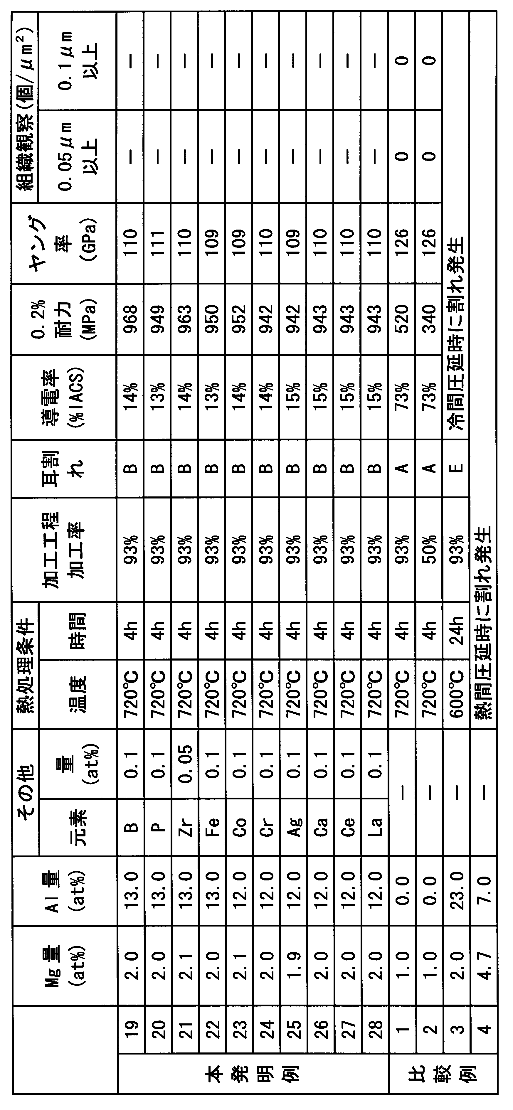
Mgの含有量およびAlの含有量が本実施形態で規定された範囲よりも少ない比較例1、2においては、ヤング率が126GPa,126GPaと比較的高く、かつ0.2%耐力が520MPa、340MPaと低い値を示した。従って、比較例1、2においては、弾性エネルギー係数(σ0.2
2/2E)が低く、塑性変形しやすい。このため、端子、コネクタ、リレー等の電子電気部品には不適であると判断される。
Alの含有量が本実施形態で規定された範囲よりも多い比較例3においては、冷間圧延時に大きな耳割れが発生し、その後の特性評価を実施することが不可能であった。
Mgの含有量が本実施形態で規定された範囲よりも多い比較例4においては、熱間圧延時に割れが発生し、その後の特性評価を実施することが不可能であった。
Alの含有量が本実施形態で規定された範囲よりも多い比較例3においては、冷間圧延時に大きな耳割れが発生し、その後の特性評価を実施することが不可能であった。
Mgの含有量が本実施形態で規定された範囲よりも多い比較例4においては、熱間圧延時に割れが発生し、その後の特性評価を実施することが不可能であった。
これに対して、本発明例1~28においては、いずれもヤング率が120GPa以下と低く、かつ0.2%耐力が600MPa以上であった。このため、弾性エネルギー係数(σ0.2
2/2E)が高く、弾力性に優れている。従って、端子、コネクタ、リレー等の電子電気部品に適している。
また、組成が同一で加工率が異なる本発明例6、12を比較すると、加工率を上昇させることによって、0.2%耐力を向上させることが可能であることが確認される。
また、組成が同一で加工率が異なる本発明例6、12を比較すると、加工率を上昇させることによって、0.2%耐力を向上させることが可能であることが確認される。
以上、本発明例によれば、低ヤング率、高耐力、高導電性を有し、端子、コネクタやリレー等の電子電気部品に適した電子機器用銅合金を提供できることが確認された。
本実施形態の電子機器用銅合金及び電子機器用銅合金圧延材は、低ヤング率、高耐力、及び高導電性を有する。このため、端子、コネクタ、及びリレー等の電子電気部品に好適に適応される。
S02 加熱工程
S03 急冷工程
S04 加工工程
S03 急冷工程
S04 加工工程
Claims (11)
- Mgを1.3原子%以上2.6原子%未満の範囲で含み、かつAlを6.7原子%以上20原子%以下の範囲で含み、残部が実質的にCu及び不可避不純物であることを特徴とする電子機器用銅合金。
- さらに、Zn,Sn,Si,Mn,及びNiから選択される1種以上を含み、その含有量が0.05原子%以上5原子%以下であることを特徴とする請求項1に記載の電子機器用銅合金。
- さらに、B,P,Zr,Fe,Co,Cr,Ag,Ca,及び希土類元素から選択される1種以上を含み、その含有量が0.01原子%以上1原子%以下であることを特徴とする請求項1又は2に記載の電子機器用銅合金。
- 0.2%耐力σ0.2が400MPa以上であることを特徴とする請求項1~3のいずれか一項に記載の電子機器用銅合金。
- ヤング率Eが125GPa以下であることを特徴とする請求項1~4のいずれか一項に記載の電子機器用銅合金。
- 走査型電子顕微鏡で観察される粒径0.1μm以上の金属間化合物の平均個数が、10個/μm2以下であることを特徴とする請求項1~5のいずれか一項に記載の電子機器用銅合金。
- 銅素材を500℃以上1000℃以下の温度にまで加熱する加熱工程と、
加熱された前記銅素材を、200℃/min以上の冷却速度で、200℃以下の温度まで冷却する急冷工程と、
急冷された前記銅素材を加工する加工工程を備え、
前記銅素材は、Mgを1.3原子%以上2.6原子%未満の範囲で含み、かつAlを6.7原子%以上20原子%以下の範囲で含み、残部が実質的にCu及び不可避不純物である銅合金からなることを特徴とする請求項1~6のいずれか一項に記載の電子機器用銅合金の製造方法。 - 前記銅素材を構成する銅合金が、さらに、Zn,Sn,Si,Mn,及びNiから選択される1種以上を含み、その含有量が0.05原子%以上5原子%以下であることを特徴とする請求項7に記載の電子機器用銅合金の製造方法。
- 前記銅素材を構成する銅合金が、さらに、B,P,Zr,Fe,Co,Cr,Ag,Ca,及び希土類元素から選択される1種以上を含み、その含有量が0.01原子%以上1原子%以下である銅合金であることを特徴とする請求項7又は8に記載の電子機器用銅合金の製造方法。
- 請求項1~6のいずれか一項に記載の電子機器用銅合金からなり、
圧延方向のヤング率Eが125GPa以下、圧延方向の0.2%耐力σ0.2が400MPa以上であることを特徴とする電子機器用銅合金圧延材。 - 端子、コネクタ、又はリレーとして使用されることを特徴とする請求項10に記載の電子機器用銅合金圧延材。
Priority Applications (2)
| Application Number | Priority Date | Filing Date | Title |
|---|---|---|---|
| CN201180057533.8A CN103228804B (zh) | 2010-12-03 | 2011-11-24 | 电子设备用铜合金、电子设备用铜合金的制造方法及电子设备用铜合金轧材 |
| US13/990,939 US20130284327A1 (en) | 2010-12-03 | 2011-11-24 | Copper alloy for electronic device, method of producing copper alloy for electronic device, and copper alloy rolled material for electronic device |
Applications Claiming Priority (2)
| Application Number | Priority Date | Filing Date | Title |
|---|---|---|---|
| JP2010270890A JP5712585B2 (ja) | 2010-12-03 | 2010-12-03 | 電子機器用銅合金、電子機器用銅合金の製造方法及び電子機器用銅合金圧延材 |
| JP2010-270890 | 2010-12-03 |
Publications (1)
| Publication Number | Publication Date |
|---|---|
| WO2012073777A1 true WO2012073777A1 (ja) | 2012-06-07 |
Family
ID=46171719
Family Applications (1)
| Application Number | Title | Priority Date | Filing Date |
|---|---|---|---|
| PCT/JP2011/077011 Ceased WO2012073777A1 (ja) | 2010-12-03 | 2011-11-24 | 電子機器用銅合金、電子機器用銅合金の製造方法及び電子機器用銅合金圧延材 |
Country Status (5)
| Country | Link |
|---|---|
| US (1) | US20130284327A1 (ja) |
| JP (1) | JP5712585B2 (ja) |
| CN (1) | CN103228804B (ja) |
| TW (1) | TWI591191B (ja) |
| WO (1) | WO2012073777A1 (ja) |
Cited By (2)
| Publication number | Priority date | Publication date | Assignee | Title |
|---|---|---|---|---|
| CN103290254A (zh) * | 2013-05-07 | 2013-09-11 | 锡山区羊尖泓之盛五金厂 | 一种耐高温超导铜线及其制备方法 |
| CN111334729A (zh) * | 2020-02-28 | 2020-06-26 | 交大材料科技(江苏)研究院有限公司 | 一种高密度纳米孪晶高性能镍铝青铜合金板材及其制备方法 |
Families Citing this family (17)
| Publication number | Priority date | Publication date | Assignee | Title |
|---|---|---|---|---|
| JP5045784B2 (ja) * | 2010-05-14 | 2012-10-10 | 三菱マテリアル株式会社 | 電子機器用銅合金、電子機器用銅合金の製造方法及び電子機器用銅合金圧延材 |
| JP5903842B2 (ja) | 2011-11-14 | 2016-04-13 | 三菱マテリアル株式会社 | 銅合金、銅合金塑性加工材及び銅合金塑性加工材の製造方法 |
| CN103388089B (zh) * | 2013-04-25 | 2015-06-17 | 刘春忠 | 电流通、断金属材料及其用途 |
| CN107531527B (zh) * | 2015-05-18 | 2021-04-09 | 三菱电机株式会社 | 水处理系统及水处理方法 |
| JP6736869B2 (ja) * | 2015-11-09 | 2020-08-05 | 三菱マテリアル株式会社 | 銅合金素材 |
| CN106834790A (zh) * | 2015-12-03 | 2017-06-13 | 黄波 | 一种Gu-Gd-Au-B合金导线及其制备方法 |
| CN106834787A (zh) * | 2015-12-03 | 2017-06-13 | 黄波 | 一种Gu-Pm-Au-B合金导线及其制备方法 |
| CN106834788A (zh) * | 2015-12-03 | 2017-06-13 | 黄波 | 一种含钐元素抗拉伸铜合金导线及其制备方法 |
| CN106834789A (zh) * | 2015-12-03 | 2017-06-13 | 黄波 | 一种Gu-Ce-Au-B合金导线及其制备方法 |
| CN108598058B (zh) * | 2017-12-21 | 2020-05-19 | 汕头市骏码凯撒有限公司 | 一种铜合金键合丝及其制造方法 |
| CN108162564A (zh) * | 2018-01-23 | 2018-06-15 | 东北大学 | 用于薄规格电连接器端子的铜钢铜复合材料及其制备方法 |
| CN109022878B (zh) * | 2018-09-11 | 2020-12-22 | 广东美的制冷设备有限公司 | 用于空调消音降噪的泡沫合金及其制备方法和应用 |
| CN111192704A (zh) * | 2019-12-30 | 2020-05-22 | 南通南平电子科技有限公司 | 一种耐弯折的无座板片式电容引线 |
| CN114951609B (zh) * | 2022-04-13 | 2024-04-19 | 佛山市陶本科技有限公司 | 具有均匀闭孔的泡沫铝板及其制备方法 |
| CN115786764B (zh) * | 2022-11-22 | 2023-12-22 | 广州番禺职业技术学院 | 一种铜镜材料及其制备方法 |
| CN117604321B (zh) * | 2024-01-22 | 2024-03-29 | 西安稀有金属材料研究院有限公司 | 一种完全共格氧化物弥散强化铜基复合材料及其制备方法 |
| CN120452906B (zh) * | 2025-06-16 | 2025-11-07 | 西安中实金属有限公司 | 一种耐腐蚀铜槽线及其防电化学腐蚀工艺 |
Citations (5)
| Publication number | Priority date | Publication date | Assignee | Title |
|---|---|---|---|---|
| JPH06100983A (ja) * | 1992-09-22 | 1994-04-12 | Nippon Steel Corp | 高ヤング率・高降伏強度を有するtabテープ用金属箔およびその製造方法 |
| JPH06100984A (ja) * | 1992-09-22 | 1994-04-12 | Nippon Steel Corp | バネ限界値と形状凍結性に優れたバネ用材料及びその製造方法 |
| JP2004225060A (ja) * | 2002-11-25 | 2004-08-12 | Dowa Mining Co Ltd | 銅合金およびその製造方法 |
| JP2009228013A (ja) * | 2008-03-19 | 2009-10-08 | Dowa Metaltech Kk | 銅合金板材およびその製造方法 |
| JP2010053445A (ja) * | 2008-08-01 | 2010-03-11 | Mitsubishi Materials Corp | フラットパネルディスプレイ用配線膜形成用スパッタリングターゲット |
Family Cites Families (7)
| Publication number | Priority date | Publication date | Assignee | Title |
|---|---|---|---|---|
| US4715910A (en) * | 1986-07-07 | 1987-12-29 | Olin Corporation | Low cost connector alloy |
| SE525460C2 (sv) * | 2002-02-28 | 2005-02-22 | Sandvik Ab | Användning av en kopparlegering i uppkolande miljöer |
| EP1803829B1 (en) * | 2004-08-17 | 2013-05-22 | Kabushiki Kaisha Kobe Seiko Sho | Copper alloy plate for electric and electronic parts having bendability |
| DE602006002573D1 (de) * | 2005-09-09 | 2008-10-16 | Ngk Insulators Ltd | Kupfer Legierungblech mit Nickel und Beryllium und Verfahren zur Herstellung derselben |
| EP2154257B1 (en) * | 2007-03-30 | 2016-10-05 | JX Nippon Mining & Metals Corporation | Cu-ni-si-based alloy for electronic material |
| EP2248921A4 (en) * | 2008-01-31 | 2011-03-16 | Furukawa Electric Co Ltd | COPPER ALLOY MATERIAL FOR ELECTRICAL / ELECTRONIC COMPONENT AND METHOD FOR PRODUCING THE COPPER ALLOY MATERIAL |
| JP5045784B2 (ja) * | 2010-05-14 | 2012-10-10 | 三菱マテリアル株式会社 | 電子機器用銅合金、電子機器用銅合金の製造方法及び電子機器用銅合金圧延材 |
-
2010
- 2010-12-03 JP JP2010270890A patent/JP5712585B2/ja not_active Expired - Fee Related
-
2011
- 2011-11-24 WO PCT/JP2011/077011 patent/WO2012073777A1/ja not_active Ceased
- 2011-11-24 US US13/990,939 patent/US20130284327A1/en not_active Abandoned
- 2011-11-24 CN CN201180057533.8A patent/CN103228804B/zh not_active Expired - Fee Related
- 2011-11-28 TW TW100143571A patent/TWI591191B/zh not_active IP Right Cessation
Patent Citations (5)
| Publication number | Priority date | Publication date | Assignee | Title |
|---|---|---|---|---|
| JPH06100983A (ja) * | 1992-09-22 | 1994-04-12 | Nippon Steel Corp | 高ヤング率・高降伏強度を有するtabテープ用金属箔およびその製造方法 |
| JPH06100984A (ja) * | 1992-09-22 | 1994-04-12 | Nippon Steel Corp | バネ限界値と形状凍結性に優れたバネ用材料及びその製造方法 |
| JP2004225060A (ja) * | 2002-11-25 | 2004-08-12 | Dowa Mining Co Ltd | 銅合金およびその製造方法 |
| JP2009228013A (ja) * | 2008-03-19 | 2009-10-08 | Dowa Metaltech Kk | 銅合金板材およびその製造方法 |
| JP2010053445A (ja) * | 2008-08-01 | 2010-03-11 | Mitsubishi Materials Corp | フラットパネルディスプレイ用配線膜形成用スパッタリングターゲット |
Cited By (2)
| Publication number | Priority date | Publication date | Assignee | Title |
|---|---|---|---|---|
| CN103290254A (zh) * | 2013-05-07 | 2013-09-11 | 锡山区羊尖泓之盛五金厂 | 一种耐高温超导铜线及其制备方法 |
| CN111334729A (zh) * | 2020-02-28 | 2020-06-26 | 交大材料科技(江苏)研究院有限公司 | 一种高密度纳米孪晶高性能镍铝青铜合金板材及其制备方法 |
Also Published As
| Publication number | Publication date |
|---|---|
| TWI591191B (zh) | 2017-07-11 |
| JP2012117142A (ja) | 2012-06-21 |
| JP5712585B2 (ja) | 2015-05-07 |
| TW201235484A (en) | 2012-09-01 |
| CN103228804A (zh) | 2013-07-31 |
| CN103228804B (zh) | 2016-05-25 |
| US20130284327A1 (en) | 2013-10-31 |
Similar Documents
| Publication | Publication Date | Title |
|---|---|---|
| JP5045784B2 (ja) | 電子機器用銅合金、電子機器用銅合金の製造方法及び電子機器用銅合金圧延材 | |
| JP5712585B2 (ja) | 電子機器用銅合金、電子機器用銅合金の製造方法及び電子機器用銅合金圧延材 | |
| JP5045783B2 (ja) | 電子機器用銅合金、電子機器用銅合金の製造方法及び電子機器用銅合金圧延材 | |
| US10032536B2 (en) | Copper alloy for electronic device, method for producing copper alloy for electronic device, and copper alloy rolled material for electronic device | |
| TWI513833B (zh) | 電子機器用銅合金、電子機器用銅合金之製造方法、電子機器銅合金用塑性加工材、以及電子機器用零件 | |
| JP5903832B2 (ja) | 電子機器用銅合金、電子機器用銅合金の製造方法、電子機器用銅合金圧延材及び電子機器用部品 | |
| JP5910004B2 (ja) | 電子機器用銅合金、電子機器用銅合金の製造方法、電子機器用銅合金塑性加工材および電子機器用部品 | |
| JP5903839B2 (ja) | 電子機器用銅合金、電子機器用銅合金の製造方法、電子機器用銅合金塑性加工材および電子機器用部品 | |
| JP5703975B2 (ja) | 電子機器用銅合金、電子機器用銅合金の製造方法及び電子機器用銅合金圧延材 | |
| JP5045782B2 (ja) | 電子機器用銅合金、電子機器用銅合金の製造方法及び電子機器用銅合金圧延材 |
Legal Events
| Date | Code | Title | Description |
|---|---|---|---|
| 121 | Ep: the epo has been informed by wipo that ep was designated in this application |
Ref document number: 11845273 Country of ref document: EP Kind code of ref document: A1 |
|
| NENP | Non-entry into the national phase |
Ref country code: DE |
|
| WWE | Wipo information: entry into national phase |
Ref document number: 13990939 Country of ref document: US |
|
| 122 | Ep: pct application non-entry in european phase |
Ref document number: 11845273 Country of ref document: EP Kind code of ref document: A1 |