WO2012073448A1 - 固体撮像装置 - Google Patents
固体撮像装置 Download PDFInfo
- Publication number
- WO2012073448A1 WO2012073448A1 PCT/JP2011/006457 JP2011006457W WO2012073448A1 WO 2012073448 A1 WO2012073448 A1 WO 2012073448A1 JP 2011006457 W JP2011006457 W JP 2011006457W WO 2012073448 A1 WO2012073448 A1 WO 2012073448A1
- Authority
- WO
- WIPO (PCT)
- Prior art keywords
- period
- gate
- signal
- control unit
- voltage
- Prior art date
- Legal status (The legal status is an assumption and is not a legal conclusion. Google has not performed a legal analysis and makes no representation as to the accuracy of the status listed.)
- Ceased
Links
Images












Classifications
-
- H—ELECTRICITY
- H04—ELECTRIC COMMUNICATION TECHNIQUE
- H04N—PICTORIAL COMMUNICATION, e.g. TELEVISION
- H04N25/00—Circuitry of solid-state image sensors [SSIS]; Control thereof
- H04N25/50—Control of the SSIS exposure
- H04N25/57—Control of the dynamic range
- H04N25/571—Control of the dynamic range involving a non-linear response
- H04N25/573—Control of the dynamic range involving a non-linear response the logarithmic type
-
- H—ELECTRICITY
- H04—ELECTRIC COMMUNICATION TECHNIQUE
- H04N—PICTORIAL COMMUNICATION, e.g. TELEVISION
- H04N25/00—Circuitry of solid-state image sensors [SSIS]; Control thereof
- H04N25/50—Control of the SSIS exposure
- H04N25/57—Control of the dynamic range
- H04N25/571—Control of the dynamic range involving a non-linear response
- H04N25/575—Control of the dynamic range involving a non-linear response with a response composed of multiple slopes
-
- H—ELECTRICITY
- H04—ELECTRIC COMMUNICATION TECHNIQUE
- H04N—PICTORIAL COMMUNICATION, e.g. TELEVISION
- H04N25/00—Circuitry of solid-state image sensors [SSIS]; Control thereof
- H04N25/50—Control of the SSIS exposure
- H04N25/57—Control of the dynamic range
- H04N25/58—Control of the dynamic range involving two or more exposures
- H04N25/581—Control of the dynamic range involving two or more exposures acquired simultaneously
- H04N25/583—Control of the dynamic range involving two or more exposures acquired simultaneously with different integration times
Definitions
- the present invention relates to a solid-state imaging device including a pixel circuit having a linear characteristic when a low luminance light is incident and a logarithmic photoelectric characteristic when a high luminance light is incident.
- a solid-state imaging device including a pixel circuit including an embedded photoelectric conversion element (hereinafter referred to as “PD”) is known.
- PD embedded photoelectric conversion element
- the PD when high-intensity light is incident, the PD enters a subthreshold state, and the signal charge is accumulated while flowing part of the signal charge through a floating diffusion layer (hereinafter referred to as “FD”). Thereby, PD has logarithmic characteristics.
- the low-luminance light when the low-luminance light is incident, the PD does not enter the subthreshold state and accumulates all signal charges. Thereby, PD has a linear characteristic. Therefore, the photoelectric conversion characteristics of the pixel circuit have two characteristics (linear log characteristics), with the linear characteristic portion showing the linear characteristic on the low luminance side and the logarithmic characteristic portion showing the logarithmic characteristic on the high luminance side, at the inflection point. become.
- Patent Document 1 there is no description about controlling the sensitivity of the logarithmic characteristic portion of the photoelectric conversion characteristic.
- An object of the present invention is to provide a solid-state imaging device capable of controlling the sensitivity of the logarithmic characteristic portion of the linear log characteristic.
- a solid-state imaging device is a solid-state imaging device including a pixel circuit having a linear log characteristic including a linear characteristic unit that exhibits linear characteristics on a low luminance side and a logarithmic characteristic unit that exhibits logarithmic characteristics on a high luminance side.
- the pixel circuit includes a photodiode that accumulates signal charges according to an incident light amount, a floating diffusion layer, and a transfer transistor that transfers the signal charges accumulated in the photodiode to the floating diffusion layer.
- a control unit is provided that changes the sensitivity of the logarithmic characteristic unit by applying a plurality of voltages to the gate of the transfer transistor during an exposure period of exposure.
- FIG. 1 is an overall configuration diagram of a solid-state imaging device according to an embodiment of the present invention.
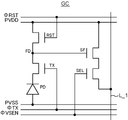
- FIG. 2 is a circuit diagram of the pixel circuit shown in FIG. 1.
- 6 is a timing chart of a pixel circuit when a transfer transistor is driven with an intermediate voltage during the entire exposure period.
- 4 is a graph showing photoelectric conversion characteristics of a pixel circuit driven according to the timing chart of FIG. 3.
- FIG. 4 is an energy band diagram of a pixel circuit corresponding to time t0 in FIG.
- FIG. 4 is an energy band diagram of a pixel circuit corresponding to time t1 in FIG.
- FIG. 4 is an energy band diagram of a pixel circuit corresponding to time t2 in FIG.
- FIG. 4 is an energy band diagram of a pixel circuit corresponding to time t3 in FIG.
- FIG. 4 is an energy band diagram of a pixel circuit corresponding to time t4 in FIG.
- FIG. 2 is a circuit diagram of the column ADC shown in FIG. 1. It is a timing chart of column ADC shown in FIG. 3 is a graph showing photoelectric conversion characteristics when sensitivity is changed in the pixel circuit shown in FIG. 2. 3 is a timing chart of a transfer transistor in the first embodiment of the present invention.
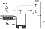
- FIG. 16 is an energy band diagram of a pixel circuit corresponding to time t0 in FIG.
- FIG. 16 is an energy band diagram of the pixel circuit corresponding to time t1 in FIG.
- FIG. 16 is an energy band diagram of the pixel circuit corresponding to time t2 in FIG. 15.
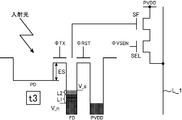
- FIG. 16 is an energy band diagram of a pixel circuit corresponding to time t3 in FIG.
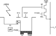
- FIG. 16 is an energy band diagram of the pixel circuit corresponding to time t4 in FIG. 15.
- FIG. 16 is an energy band diagram of the pixel circuit corresponding to time t5 in FIG.
- FIG. 25 is an energy band diagram of the pixel circuit corresponding to time t0 in FIG. 24.
- FIG. 25 is an energy band diagram of the pixel circuit corresponding to time t1 in FIG. 24.
- FIG. 1 is an overall configuration diagram of a solid-state imaging device according to an embodiment of the present invention.
- the solid-state imaging device is a columnar parallel AD conversion type (column AD conversion type) CMOS (Complementary Metal Oxide Semiconductor) type solid-state imaging device, which includes a pixel array unit 1, a row decoder 2, a column.
- TG timing generator
- the pixel array unit 1 to the output terminal 13 are integrated on one chip, and constitute a solid-state imaging device.
- the solid-state imaging device may be configured by integrating the pixel array unit 1 to the control unit 14 on one chip.
- the pixel array unit 1 includes a plurality of pixel circuits GC (not shown) arranged in a matrix in M (M is a positive integer of 2 or more) rows ⁇ N (N is a positive integer of 2 or more) columns. ing. In the example of FIG. 1, the pixel circuits GC are arranged in a matrix of 14 rows ⁇ 17 columns.
- the row decoder 2 includes, for example, a vertical scanning circuit and a driver circuit.
- the vertical scanning circuit is configured by, for example, a shift register, and performs vertical scanning of the pixel array unit 1 by cyclically selecting each row of the pixel array unit 1 in synchronization with a vertical synchronization signal output from the TG 6.
- the driver circuit generates a pixel control signal and outputs the pixel control signal to each pixel circuit GC belonging to the row selected by the vertical scanning circuit, thereby driving each pixel circuit GC.
- the column ADC array unit 3 includes N column ADCs 31 corresponding to the respective columns of the pixel array unit 1.
- the column ADC 31 is connected to the pixel circuit GC of each column via the vertical signal line L_1 corresponding to each column of the pixel array unit 1, and receives a noise signal and a signal signal from the pixel circuit GC of the row selected by the vertical scanning circuit. read out. Then, the column ADC 31 performs a correlated double sampling process on the read noise signal and signal signal to acquire a video signal.
- the column ADC 31 performs analog-digital conversion processing on the acquired video signal and holds the digital video signal.
- the column decoder 4 is composed of, for example, a shift register, and cyclically selects the column ADC 31 of each column in one horizontal scanning period by outputting a column selection signal synchronized with the horizontal synchronization signal output from the TG 6.
- the column ADC array unit 3 is horizontally scanned, and the digital video signals held by the column ADCs 31 of each column are sequentially output to the sense amplifier 8.
- the PLL 5 multiplies a clock signal (SYSCLK) supplied from an external device (for example, the control unit 14) via the clock terminal 11, and outputs the multiplied signal to the TG 6.
- SYSCLK clock signal supplied from an external device (for example, the control unit 14) via the clock terminal 11, and outputs the multiplied signal to the TG 6.
- a 54 MHz clock signal is supplied to the clock terminal 11, and the PLL 5 multiplies the 54 MHz clock signal by 2 and supplies the 108 MHz clock signal to the TG 6.
- the TG 6 generates timing signals necessary for controlling the solid-state imaging device, such as a vertical synchronization signal and a horizontal synchronization signal, according to the clock signal supplied from the PLL 5, and controls the entire solid-state imaging device.
- the TG 6 includes a register for storing a setting value of the timing signal.
- setting values are written in the register by, for example, serial communication with an external device (for example, the control unit 14) connected via the control terminal 12.
- an external device for example, the control unit 14
- the set value for example, a later-described transfer transistor TX (see FIG. 2) is driven in an intermediate state between a conductive state and a non-conductive state, and an intermediate voltage value for half-opening the gate of the transfer transistor TX is determined. For example.
- the pixel array unit 1 includes, for example, a plurality of types of pixel circuits GC for acquiring video signals of a plurality of color components such as R (red), G (green), and B (blue). They are regularly arranged according to a predetermined arrangement method such as an arrangement. Therefore, the TG 6 stores a predetermined setting value that defines an intermediate voltage for each type of the pixel circuit GC in the register. The TG 6 controls the DAC 7 and the row decoder 2 so that each pixel circuit GC is driven by an intermediate voltage defined by a set value corresponding to the type of the pixel circuit GC.
- the TG 6 stores in advance which type of pixel circuit GC is arranged in each row and column of the pixel array unit 1. When one row with the row decoder 2 is selected, the TG 6 specifies which type of pixel circuit GC is arranged in each column of the row, and outputs a setting value corresponding to the specified type to the DAC 7.
- TG6 converts the set value to DAC7 from digital to analog.
- the set value that has been converted from digital to analog is input to the row decoder 2.
- the row decoder 2 Under the control of TG6, the row decoder 2 outputs an intermediate voltage defined by the input set value to the transfer transistor TX (see FIG. 2) of the pixel circuit GC of each selected column.
- each pixel circuit GC can obtain an appropriate dynamic range according to its type.
- the DAC (digital analog converter) 7 converts a digital signal output from the TG 6 into an analog signal and supplies the analog signal to the row decoder 2. For example, the DAC 7 converts the set value for defining the intermediate voltage output from the TG 6 into an analog signal to generate an intermediate voltage, and supplies the intermediate voltage to the row decoder 2.
- the ramp generation circuit 9 generates a ramp signal and outputs it to each column ADC 31.
- the sense amplifier 8 amplifies the digital video signal output from the column ADC array unit 3 via the horizontal signal line L_2 and outputs the amplified signal to the serializer 10.
- the column ADC 31 generates a 14-bit digital video signal, shifts the phase of the signal of each bit by 180 degrees, and signals that are shifted in phase by 180 degrees and signals that are not shifted in phase.
- a total of 28 signals consisting of are output to the sense amplifier 8. Therefore, the total number of horizontal signal lines L_2 connecting the column ADC array unit 3 and the sense amplifier 8 is 28.
- the sense amplifier 8 amplifies the signals flowing through the 28 horizontal signal lines L_2, shapes the waveform of each signal, and outputs the waveform to the serializer 10.
- the serializer 10 is composed of, for example, a serializer conforming to the LVDS (Low Voltage Differential Signalings) standard, and differentially amplifies a signal output in parallel via the 28 horizontal signal lines L_2 from the sense amplifier 8 to 14 bits. The signal is converted to serial and output to the output terminal 13. The output terminal 13 outputs a signal from the serializer 10 to the control unit 14.
- LVDS Low Voltage Differential Signalings
- the control unit 14 is configured by, for example, a dedicated hardware circuit, and changes the sensitivity of the logarithmic characteristics by applying a plurality of voltages to the gate of the transfer transistor TX during the exposure period (see FIG. 2).
- the control unit 14 writes, for example, a plurality of types of setting values into the register of the TG 6 via the control terminal 12.
- the TG 6 applies an intermediate voltage according to the written set value to the gate of the transfer transistor TX via the DAC 7 and the row decoder 2. Details of the control unit 14 will be described later.
- FIG. 2 is a circuit diagram of the pixel circuit GC shown in FIG.
- the pixel circuit GC includes a photoelectric conversion element (hereinafter referred to as “PD”), a transfer transistor (hereinafter referred to as “TX”), and a reset transistor (hereinafter referred to as “RST”). ), An amplification transistor (hereinafter referred to as “SF”), and a row selection transistor (hereinafter referred to as “SEL”).
- PD photoelectric conversion element
- TX transfer transistor
- RST reset transistor
- SF An amplification transistor
- SEL row selection transistor
- the PD receives light from the subject, generates signal charge according to the received light quantity, and accumulates it with parasitic capacitance.
- the PD has an anode connected to the source of TX, and PVSS as a driving voltage is input to the anode.
- TX is composed of, for example, nMOS (Negative Channel Metal Oxide Semiconductor), and transfers signal charges accumulated by PD to a floating diffusion layer (hereinafter referred to as “FD” floating ⁇ diffusion).
- FD floating diffusion layer
- a signal (hereinafter referred to as “ ⁇ TX”) for driving TX in a conductive state, a non-conductive state, and an intermediate state is input to the gate of TX.
- the drain of TX is connected to FD.
- VL negative voltage
- ⁇ TX becomes an intermediate voltage (hereinafter referred to as “VM”)
- VM intermediate voltage
- TX is half-opened, and TX is in an intermediate state between a conductive state and a non-conductive state.
- VH high level voltage
- FD accumulates signal charges transferred from PD. As a result, a voltage corresponding to the signal charge appears in the FD.
- RST is composed of, for example, an nMOS, ⁇ RST that is a signal for making RST conductive or non-conductive is input to a gate, PVDD that is a driving voltage is input to a drain, and a source of SF is connected through FD. Connected to the gate.
- ⁇ RST VH
- RST becomes conductive
- ⁇ RST VL
- RST then discharges the FD signal charge and resets the FD when it becomes conductive.
- PVDD and PVSS are output from a voltage source (not shown), and ⁇ RST is output from the row decoder 2.
- SF is composed of, for example, an nMOS
- the gate is connected to TX and RST via FD
- the drive voltage PVDD is input to the drain
- the source is connected to SEL.
- the SF amplifies the voltage appearing on the FD and outputs it to the SEL.
- SEL is composed of, for example, an nMOS, and a gate selection signal ⁇ VSEN is input to the gate, the drain is connected to SF, and the source is connected to the column ADC 31 of the corresponding column via the vertical signal line L_1.
- the SEL outputs the voltage amplified by the SF as an output signal to the column ADC 31 in the corresponding column via the vertical signal line L_1.
- ⁇ VSEN is output from the row decoder 2.
- FIG. 3 is a timing chart of the pixel circuit GC when the transfer transistor TX is driven with an intermediate voltage during the entire exposure period T_E.
- the exposure period is a period during which the subject is exposed, and the PD accumulates signal charges from the subject.
- the pixel circuit GC cyclically repeats the exposure period T_E and the readout period T_R, and outputs a signal signal corresponding to the signal charge accumulated in the exposure period T_E.
- ⁇ VSEN VH and SEL is in a conductive state.
- the noise level voltage V_n appearing in the FD is amplified by SF and output to the column ADC 31 as a noise signal.
- the reason why the voltage of the FD decreases from PVDD to the voltage V_n is mainly due to the influence of the parasitic capacitance between the FD and RST caused by changing ⁇ RST from VH to VL.
- the effect of ktc noise is also included. Since the ktc noise varies for each pixel circuit GC, the noise signal varies for each pixel circuit GC. Note that the voltage of the FD decreases as the amount of accumulated signal charge increases.
- ⁇ VSEN VL
- SEL is in a non-conductive state
- the output of the noise signal is stopped.
- ⁇ TX VH is set, TX becomes conductive, and the signal charge of the PD is transferred to the FD.
- the voltage of the FD decreases according to the signal charge transferred to the FD, and becomes a signal level voltage V_s.
- the voltage V_s of the FD is current amplified by SF, and is output as a signal signal to the column ADC 31 via the vertical signal line L_1.
- the output signal signal is differentiated from the noise signal by the column ADC 31, and a video signal is generated.
- the video signal has a value corresponding to the difference between the FD noise level voltage V_n and the signal level voltage V_s. Therefore, by taking the difference between the noise signal and the signal signal, a video signal from which the noise component included in the signal signal has been removed can be obtained.
- FIG. 4 is a graph showing the photoelectric conversion characteristics of the pixel circuit GC driven according to the timing chart of FIG.
- the vertical axis is a linear axis and indicates a video signal output from the pixel circuit GC
- the horizontal axis is a logarithmic axis and indicates the intensity of incident light incident on the photoelectric conversion element PD.
- the photoelectric conversion characteristics include a linear characteristic portion D1 in which the low luminance region exhibits a linear characteristic from the inflection point P1 and a logarithmic characteristic portion in which the high luminance region exhibits a logarithmic (log) characteristic. It has a linear log characteristic consisting of D2.
- the linear characteristic portion D1 rises while drawing a curve and the logarithmic characteristic portion D2 rises substantially linearly because the horizontal axis is a logarithmic axis.
- FIGS. 5 to 9 are energy band diagrams of the pixel circuit GC corresponding to the time t0 to the time t4 in FIG.
- the energy band diagrams shown in FIGS. 5 to 9 show that the voltage is higher toward the lower side.
- the signal charge accumulated in the PD becomes a certain value or more
- the signal charge can move from the PD to the FD over the energy barrier ES.
- the PD enters a subthreshold state and accumulates signal charges while leaking signal charges to the FD.
- the signal charge of the second layer L2 has a logarithmic characteristic with respect to the amount of incident light. Thereby, the linear log characteristic is realized in the exposure period T_E shown at time t0.
- ⁇ TX VH and TX is turned on. Thereby, the energy barrier ES is eliminated, and the signal charge is transferred from the PD to the FD.
- the FD accumulates signal charges including the first layer L1 and the second layer L2, and the voltage drops from the voltage V_n to the voltage V_s.
- FIG. 10 is a circuit diagram of the column ADC 31 shown in FIG.
- the column ADC includes a CDS circuit 41, a clamp unit 42, a comparison unit 43, and a latch circuit 44 in order from the upstream side.
- the CDS circuit 41 includes an inverting amplifier (hereinafter referred to as “AMP”), capacitors CIN and CF, and a switch SW1.
- AMP inverting amplifier
- the input node I_1 of the AMP is connected to the vertical signal line L_1 via the capacitor CIN.
- a capacitor CF is connected between the input and output nodes of the AMP.
- a switch SW1 is connected in parallel to the capacitor CF.
- the terminal on the vertical signal line L_1 side of the capacitor CIN is a node VPIX.
- the clamp unit 42 includes a capacitor C0 and a switch SW2.
- ⁇ CL becomes high level
- the switch SW2 is turned on, and the voltage at the node BB is clamped by the clamp voltage VCL.
- the comparison unit 43 includes switches SW3, SW4, SW5, SW6, a comparator COMP1 (hereinafter referred to as “COMP1”), a comparator COMP2 (hereinafter referred to as “COMP2”), and capacitors C1 and C2. .
- COMP1 comparator COMP1
- COMP2 comparator COMP2
- the switch SW3 is connected between the node BB and the node CC.
- the switch SW4 has one end connected to the node CC and the other end connected to a voltage source of a ramp signal (hereinafter referred to as “VRAMP”).
- VRAMP a voltage source of a ramp signal
- COMP1 has an input node (hereinafter referred to as “node DD”) connected to a node CC via a capacitor C1.
- a switch SW5 is connected between the input / output nodes of COMP1.
- the output node of COMP1 is connected to COMP2 via a capacitor C2.
- a switch SW6 is connected between the input / output nodes of COMP2.
- a latch circuit 44 is connected to the output node of COMP2 via an inverter I1.
- FIG. 11 is a timing chart of the column ADC 31 shown in FIG. Note that times t1 and t3 shown in FIG. 11 correspond to the same times in FIG.
- ⁇ PRST, ⁇ CL, ⁇ S1, and ⁇ S2 are each set to a high level for a predetermined time, and the CDS circuit 41, the clamp unit 42, and COMP1 and COMP2 are reset.
- the voltage at the node AA becomes VTH (AMP)
- the voltages at the nodes BB and CC become VCL
- the voltage at the node DD becomes VTH (COMP1).
- the voltages of the nodes AA, BB, CC, DD increase.
- the nodes AA and BB increase by ⁇ V ⁇ CIN / CF.
- the nodes CC and DD rise by ⁇ V ⁇ (CIN / CF) ⁇ C0 / (C0 + C1). That is, the CDS circuit 41 calculates a difference between the noise signal and the signal signal, and a voltage corresponding to ⁇ V indicating the difference appears at the nodes AA to DD.
- the latch circuit 44 latches the count value at that time.
- the voltage of the node CC decreases from ⁇ V ⁇ (CIN / CF) ⁇ C0 / (C0 + C1) by the voltage Va at the start of input of VRAMP. Therefore, the level of the node CC at this time corresponds to ⁇ V Has a value. Therefore, the period from time TT1 to time TT2 has a value corresponding to ⁇ V. Therefore, by counting the time from when VRAMP is input to when COMPOUT is inverted, a digital value corresponding to ⁇ V, that is, a digital value of the video signal can be obtained.
- FIG. 12 is a graph showing photoelectric conversion characteristics when the sensitivity is changed in the pixel circuit GC shown in FIG.
- the vertical axis is a linear axis and indicates a video signal output from the pixel circuit GC
- the horizontal axis is a logarithmic axis and indicates the intensity of incident light incident on the photoelectric conversion element PD.
- the photoelectric conversion characteristic C (a) is a photoelectric conversion characteristic of the pixel circuit GC in which the sensitivity shown in FIG. 4 is set as a standard.
- the photoelectric conversion characteristic C (a) when it is desired to increase the sensitivity of the linear characteristic portion D1 (a), for example, i) increase the gain of the column ADC 31, ii) decrease the input range of the column ADC 31, iii) after AD conversion It is conceivable to add digital gain to the video signal.
- CIN / CF shown in FIG. 10 may be increased.
- the amplitude of VRAMP shown in FIG. 11 may be reduced.
- the difference Vb ⁇ Va may be reduced.
- the control unit 14 that has captured the AD-converted video signal may multiply the digital video signal by a predetermined number (for example, two times or three times).
- the photoelectric conversion characteristic C (b) is obtained.
- the sensitivity of not only the linear characteristic part D1 (a) but also the logarithmic characteristic part D2 (a). Will also go up. Therefore, the dynamic range DM (b) of the photoelectric conversion characteristic C (b) is lower than the dynamic range DM (a) of the photoelectric conversion characteristic C (a).
- the sensitivity of the logarithmic characteristic portion D2 is made variable to obtain the photoelectric conversion characteristic C (c).
- the slope of the linear characteristic part D1 (c) is twice the slope of the linear characteristic part D1 (a)
- the sensitivity of the linear characteristic part D1 (c) is the linear characteristic part D1 ( It is twice that of a).
- the slope of the logarithmic characteristic portion D2 (c) is 1 ⁇ 2 of the slope of the logarithmic characteristic portion D2 (a)
- the sensitivity of the logarithmic characteristic portion D2 (c) is 1 / th of the sensitivity of the logarithmic characteristic portion D2 (a). 2
- FIG. 13 is a TX timing chart according to Embodiment 1 of the present invention.
- VD indicates the start timing of the exposure period T_E of one frame.
- (A) shows the case where the sensitivity is not changed
- (b) shows the case where the sensitivity is made lower than (a)
- (c) shows the case where the sensitivity is made lower than (b). Note that since the readout period T_R is significantly shorter than the exposure period T_E, the readout period T_R is not shown in FIG. 13, and the exposure periods T_E of the respective frames are connected.
- ⁇ TX VM is always set in the exposure period T_E of one frame, and the intermediate voltage VM is always applied to the gate of TX.
- the TX gate is half open.
- FIG. 14 shows photoelectric conversion characteristics C (a), C (b), and C (c) of the pixel circuit GC when TX is driven with ⁇ TX in FIGS. 13 (a), (b), and (c). .
- ⁇ TX VL is set, and the TX gate is closed. Therefore, the PD accumulates signal charges with linear characteristics.
- ⁇ TX VM is set, and the gate of the transfer transistor TX is half opened.
- the PD accumulates signal charges with linear log characteristics.
- the period tint_log in FIG. 15 is the second half period, and the gate of the transfer transistor TX is half open.
- the operation in the reading period T_R is the same as that in FIG.
- FIGS. 16 to 21 are energy band diagrams of the pixel circuit GC corresponding to the time t0 to the time t5 in FIG.
- the energy band diagrams shown in FIGS. 16 to 21 show that the voltage is higher toward the lower side.
- ⁇ TX VM and the gate of the transfer transistor TX is half open.
- the energy barrier ES is reduced, and the signal charge accumulated on the upper part of the PD leaks toward the FD.
- the period tint_log becomes shorter, the amount of logarithmic characteristic signal charge finally remaining in the PD deviates from the amount of logarithmic characteristic signal charge that should originally be accumulated in the PD. Therefore, as the period tint_log becomes shorter, the slope of the logarithmic characteristic portion D2 decreases, and the sensitivity of the logarithmic characteristic portion D2 becomes lower.
- the control unit 14 obtains the luminance of the subject, shortens the period tint_log as the luminance of the subject increases, and reduces the sensitivity of the logarithmic characteristic unit D2 to ensure the dynamic range.
- the control unit 14 increases the sensitivity of the logarithmic characteristic unit D2 by extending the period tint_log as the luminance of the subject decreases.
- control unit 14 may obtain the period tint_log using a function or LUT in which the relationship between the luminance of the subject and the period tint_log is determined in advance. Then, a control signal for driving TX in the obtained period tint_log may be output to TG6. The TG 6 that has received this control signal may control the row decoder 2 so that TX is driven with ⁇ TX having the period tint_log obtained by the control unit 14.
- control unit 14 may calculate an average value of video signals output from all or some of the pixel circuits GC constituting the pixel array unit 1 as the luminance of the subject.
- the control unit 14 may obtain a histogram of video signals output from all or some of the pixel circuits GC constituting the pixel array unit 1 and calculate the maximum peak of the histogram as the luminance of the subject.
- the solid-state imaging device of Embodiment 2 is characterized in that an intermediate voltage (hereinafter referred to as “VM1”) and an intermediate voltage (hereinafter referred to as “VM2”) are applied during the exposure period T_E.
- VM1 an intermediate voltage
- VM2 an intermediate voltage
- FIG. 22 is a TX timing chart according to Embodiment 2 of the present invention.
- (A) shows the case where the sensitivity is not changed
- (b) shows the case where the sensitivity is made higher than (a)
- (c) shows the case where the sensitivity is made higher than (b). Note that since the readout period T_R is significantly shorter than the exposure period T_E, the readout period T_R is not shown in FIG. 22 and the exposure periods T_E of the respective frames are connected.
- VM1 ⁇ VM2. Therefore, the TX gate is half open in both the first half period and the second half period, but the gate is opened more greatly in the second half period than in the first half period.
- VM2 is an intermediate voltage for setting the inflection point P1 of the photoelectric conversion characteristics of the pixel circuit GC to a target value.
- FIG. 23 shows photoelectric conversion characteristics C (a), C (b), and C (c) of the pixel circuit GC when TX is driven with ⁇ TX in FIGS. 22 (a), (b), and (c). .
- ⁇ TX VM1 is set, and the TX gate is half open. Therefore, the PD accumulates signal charges with linear log characteristics.
- the period tlog_sec in FIG. 24 is the second half period.
- the operation in the reading period T_R is the same as that in FIG.
- ⁇ TX VM1 is set, and the TX gate is half opened. As a result, during the first half of the exposure period T_E, TX is driven with the gate half open.
- FIGS. 25 and 26 are energy band diagrams of the pixel circuit GC corresponding to time t0 and time t1 in FIG.
- the energy band diagrams shown in FIGS. 25 and 26 indicate that the voltage is higher toward the lower side. Note that the energy band diagram at times t2, t3, and t4 shown in FIG.
- ⁇ TX VM1
- the gate of TX is half-opened, and an energy barrier ES is generated between PD and FD.
- the PD is in a subthreshold state determined by VM1 and accumulates signal charges with linear log characteristics.
- the PD accumulates signal charges belonging to the first layer L1 below VM1 with linear characteristics, and accumulates signal charges belonging to the second layer L2 above VM1 with logarithmic characteristics.
- ⁇ TX VM2
- the TX gate is further opened more than at time t0.
- the energy barrier ES becomes lower than that at time t0.
- the signal charge belonging to the second layer L2 is placed on the signal charge accumulated in the layer L1 ′ between VM1 and VM2.
- the signal charge belonging to this layer L1 ′ is the signal charge belonging to the first layer L1 at time t0.
- the signal charge of the layer L1 ′ leaks to the FD side, and the layer L1 ′ becomes logarithmic and is absorbed by the second layer L2, and eventually disappears, but if the period tlog_sec is shorter, It behaves like a logarithmic characteristic and becomes an offset of the second layer L2. Therefore, if the period tlog_sec is short, at the end of the exposure period T_E, the signal charge component accumulated in the logarithmic characteristic among the signal charges remaining in the PD increases, and the sensitivity of the logarithmic characteristic portion D2 increases.
- the sensitivity of the logarithmic characteristic portion D2 can be increased similarly. That is, the greater the difference between VM1 and VM2, the more the height of the layer L1 ′ increases, so the offset of the second layer L2 increases. Therefore, at the end of the exposure period T_E, the signal charge component accumulated in the logarithmic characteristic among the signal charges remaining in the PD increases, and the sensitivity of the logarithmic characteristic portion D2 increases.
- the sensitivity of the logarithmic characteristic portion D2 depends on the length of the period tlog_sec and the voltage difference between VM2 and VM1.
- control unit 14 obtains the brightness of the subject in the same manner as in the first embodiment, and performs control to increase the period tlog_sec as the brightness of the subject increases, and increases VM1 to reduce the voltage difference between VM1 and VM2.
- the control unit 14 executes at least one of the controls, the sensitivity of the logarithmic characteristic portion D2 is lowered and the dynamic range is secured.
- control unit 14 performs logarithmic characteristics by executing at least one of control for shortening the period tlog_sec and control for increasing the voltage difference between VM1 and VM2 by decreasing VM1 as the luminance of the subject decreases.
- the sensitivity of the part D2 is increased.
- control unit 14 may obtain the period tlog_sec using a function or LUT in which the relationship between the luminance of the subject and the period tlog_sec is determined in advance.
- VM1 may be obtained by using a function or LUT that predetermines the relationship between the luminance of the subject and the period VM1.
- a control signal for driving TX in the obtained period tlog_sec or VM1 may be output to TG6.
- the TG 6 that has received this control signal may control the row decoder 2 so that TX is driven with ⁇ TX having the period tlog_sec, VM1 obtained by the control unit 14.
- the presence / absence of a bright subject is determined, and the method of the first embodiment is used to perform control to lower the sensitivity when a bright subject exists, and the sensitivity is increased when there is no bright subject. It is characterized by performing control.
- control unit 14 shortens the period tint_log when it is determined that there is a bright subject, compared to when it is determined that there is no bright subject. Thereby, the sensitivity of the logarithmic characteristic portion D2 is lowered, and a dynamic range is secured.
- control unit 14 determines that there is no bright subject
- the control unit 14 lengthens the period tint_log compared to the case where it is determined that there is a bright subject. This increases the sensitivity of the logarithmic characteristic portion D2.
- the control unit 14 sets the period tint_log to a predetermined period T_down when a bright subject exists.
- the control unit 14 may set the period tint_log to a predetermined period T_up when there is no bright subject.
- the entire period of the exposure period T_E may be set as the period tint_log. In this way, it is possible to maximize the sensitivity when there is no bright subject.
- control unit 14 may determine the presence or absence of a bright subject based on the average value of the video signal output from each pixel circuit GC.
- control unit 14 obtains an average value of the video signals output from all or some of the pixel circuits GC configuring the pixel array unit 1, compares the average value with a specified value V_th1, and calculates the average value. Can be determined that there is a bright subject, and if the average value is less than the specified value V_th1, it can be determined that there is no bright subject.
- a predetermined level on the high luminance side of the logarithmic characteristic portion D2 shown in FIG. 4 may be adopted.
- control unit 14 obtains a histogram of video signals output from all or some of the pixel circuits GC constituting the pixel array unit 1 and determines whether or not the subject is bright based on this histogram. Good.
- the control unit 14 obtains a graph of the histogram of the video signal that defines the gradation value of the video signal on the horizontal axis and the frequency on the vertical axis, identifies the peak on the highest gradation side from this graph, If the tone value is equal to or greater than the specified value V_th2, it is determined that the subject is bright, and if the peak tone value is less than the specified value V_th2, the subject is determined to be dark.
- the prescribed value V_th2 the prescribed value V_th1 shown in FIG. 4 may be adopted, a value slightly lower than the prescribed value V_th1 may be adopted, or a value slightly higher than the prescribed value V_th1 may be adopted. Good.
- control unit 14 obtains a total value of the frequencies of the gradation values higher than the specified value V_th1 in the histogram, and determines that a bright subject exists if the total value is equal to or greater than the specified value V_th3. If it is less than the prescribed value Vth_3, it may be determined that there is no bright subject.
- the specified value V_th3 for example, the number of pixel circuits GC that output a video signal having a gradation value equal to or higher than the specified value V_th1 with respect to the number of all the pixel circuits GC configuring the pixel array unit 1 is predetermined. What is necessary is just to employ
- the dynamic range can be ensured when a bright subject exists, and the sensitivity can be increased when there is no bright subject.
- the presence / absence of a bright subject is determined, and the method of the second embodiment is used to perform control to lower the sensitivity when a bright subject exists, and the sensitivity is increased when there is no bright subject. It is characterized by performing control.
- the description of the same elements as in the first to third embodiments is omitted.
- control unit 14 determines the presence or absence of a bright subject using the same method as in the third embodiment. Then, the control unit 14 determines whether or not there is a bright subject, and when it is determined that there is a bright subject, the control unit 14 lengthens the period tlog_sec compared to when it is determined that there is no bright subject.
- the control unit 14 sets the period tlog_sec to a predetermined period T_up.
- the control unit 14 sets the period tlog_sec to a predetermined period T_down.
- the period T_up > the period T_down.
- control unit 14 may reduce the voltage difference between the VM1 and the VM2 when it is determined that a bright subject exists, compared to a case where it is determined that there is no bright subject.
- control unit 14 may increase the voltage difference between VM1 and VM2 as compared with the case where it is determined that there is a bright subject.
- VM2 is fixed in order to set the inflection point P1 to a desired value
- the value of VM1 is a larger value VM1_big than when there is no bright subject.
- the voltage difference between VM1 and VM2 may be reduced.
- the value of VM1 is set to the value VM1_small and the voltage difference between VM1 and VM2 is increased.
- the value VM1_big a predetermined value beforehand, when ensuring a dynamic range.
- a suitable value determined in advance for increasing the sensitivity of the logarithmic characteristic portion D2 may be adopted.
- control for changing the period tlog_sec and the control for changing the voltage difference between VM1 and VM2 may be combined.
- a solid-state image pickup device is a solid-state image pickup device including a pixel circuit having a linear log characteristic including a linear characteristic portion having a linear characteristic on a low luminance side and a logarithmic characteristic portion having a logarithmic characteristic on a high luminance side.
- the pixel circuit includes a photodiode that accumulates signal charges according to an incident light amount, a floating diffusion layer, and a transfer transistor that transfers the signal charges accumulated in the photodiode to the floating diffusion layer.
- a control unit is provided that changes the sensitivity of the logarithmic characteristic unit by applying a plurality of voltages to the gate of the transfer transistor during an exposure period of exposure.
- the control unit applies the intermediate voltage to the gate of the transfer transistor at least at the last period of the exposure period to half-open the gate, and changes the period of applying the intermediate voltage to change the logarithmic characteristic. It is preferable to change the sensitivity of the part.
- the intermediate voltage is applied to the gate of the transfer transistor and the gate is half-opened.
- the sensitivity of the logarithmic characteristic portion is changed by changing the period during which the intermediate voltage is applied.
- the signal charge finally remaining in the photoelectric conversion element at the end of the exposure period approaches the amount of signal charge having the logarithmic characteristic that should be inherent. It will be. Therefore, the sensitivity of the logarithmic characteristic portion can be increased by lengthening the period during which the intermediate voltage is applied.
- the last period refers to the last period when the exposure period is divided into a plurality of periods.
- the exposure period is divided into two periods, a first half period and a second half period
- the second half period corresponds to at least the last period.
- control unit divides the exposure period into two periods, applies a voltage for closing the gate to the gate in the first half period, and applies the intermediate voltage to the gate in the second half period.
- the control unit applies a first intermediate voltage to the gate to partially open the gate, and then applies a second intermediate voltage higher than the first intermediate voltage to the gate.
- the sensitivity of the logarithmic characteristic portion is changed by performing at least one of control for changing the period for applying the second intermediate voltage and changing the voltage difference between the first intermediate voltage and the second intermediate voltage by further opening the gate. It is preferable to make it.
- the gate is further opened. Therefore, at the end of the exposure period, the signal charge component having the logarithmic characteristic among the signal charges remaining in the photoelectric conversion element can be increased, and the sensitivity of the logarithmic characteristic portion can be increased.
- the sensitivity of the logarithmic characteristic portion can be changed by performing at least one of control for changing the time for applying the second intermediate voltage and control for changing the voltage difference.
- the control unit determines whether or not there is a bright subject.
- the controller applies a period during which the intermediate voltage is applied compared to when the bright subject is determined not to exist. It is preferable to shorten it.
- the period during which the intermediate voltage is applied is shortened, so that the sensitivity of the logarithmic characteristic portion is lowered and the dynamic range can be secured.
- the period of applying the intermediate voltage is lengthened, so that the sensitivity of the logarithmic characteristic portion can be increased.
- the control unit determines whether or not a bright subject exists, and determines that the bright subject exists, and applies a second intermediate voltage compared to a case where the bright subject does not exist. It is preferable to perform at least one of control for increasing the voltage difference and control for reducing the voltage difference as compared with a case where it is determined that the bright subject does not exist.
- control unit determines whether or not the bright subject exists based on an average value of pixel signals output from each pixel circuit.
- control unit determines the presence / absence of the bright subject based on a histogram of pixel signals output from each pixel circuit.
Landscapes
- Engineering & Computer Science (AREA)
- Multimedia (AREA)
- Signal Processing (AREA)
- Physics & Mathematics (AREA)
- Nonlinear Science (AREA)
- Transforming Light Signals Into Electric Signals (AREA)
- Solid State Image Pick-Up Elements (AREA)
- Studio Devices (AREA)
Abstract
露光期間T_Eの前半期間の時刻t0において、φTX=VLに設定され、転送トランジスタTXのゲートが閉じられている。そのため、PDはリニア特性で信号電荷を蓄積する。露光期間T_Eの後半期間(期間tint_log)の時刻t1において、φTX=VMに設定され、転送トランジスタTXのゲートが半開にされる。これにより、PDは信号電荷をリニアログ特性で蓄積する。そして、期間tint_logを長くすることで対数特性部の感度を上げる。
Description
本発明は、低輝度光入射時には線形特性、高輝度光入射時には対数特性の光電変換特性を持つ画素回路を備える固体撮像装置に関するものである。
近年、埋込型の光電変換素子(以下、「PD」と記述する。)を備えた画素回路を備える固体撮像装置が知られている。このような固体撮像装置においては、露光期間中に転送トランジスタを導通状態と非導通状態との中間状態で駆動させ、PDに蓄積される信号電荷を対数的に圧縮し、ダイナミックレンジを広げることが行われている(例えば、特許文献1)。
つまり、高輝度光入射時にはPDがサブスレショルド状態になり、信号電荷の一部を浮遊拡散層(以下、「FD」と記述する。)に流しつつ信号電荷を蓄積する。これにより、PDは対数特性を持つ。一方、低輝度光入射時にはPDがサブスレショルド状態にならず、信号電荷を全て蓄積する。これにより、PDは線形特性を持つ。よって、画素回路の光電変換特性は、変極点を境に、低輝度側が線形特性を示す線形特性部と、高輝度側が対数特性を示す対数特性部との2つの特性(リニアログ特性)を持つことになる。
しかしながら、特許文献1では、光電変換特性の対数特性部の感度を制御することについての記載が全く行われていない。
本発明の目的は、リニアログ特性の対数特性部の感度を制御することができる固体撮像装置を提供することである。
本発明の一局面による固体撮像装置は、低輝度側が線形特性を示す線形特性部と、高輝度側が対数特性を示す対数特性部とを備えるリニアログ特性を持つ画素回路を備える固体撮像装置であって、前記画素回路は、入射光量に応じた信号電荷を蓄積するフォトダイオードと、浮遊拡散層と、前記フォトダイオードに蓄積された信号電荷を前記浮遊拡散層に転送する転送トランジスタとを備え、被写体を露光する露光期間において複数の電圧を前記転送トランジスタのゲートに印加することで、前記対数特性部の感度を変化させる制御部を備える。
(実施の形態1)
図1は、本発明の実施の形態における固体撮像装置の全体構成図である。図1に示すように固体撮像装置は、列並列型AD変換方式(カラムAD変換方式)のCMOS(Complementary Metal Oxide Semiconductor)型の固体撮像装置であって、画素アレイ部1、ローデコーダ2、カラムADCアレイ部3、カラムデコーダ4、PLL5、タイミングジェネレータ(以下、「TG」と記述する。)6、DAC7、センスアンプ8、ランプ生成回路9、シリアライザ10、クロック端子11、制御端子12、出力端子13、及び制御部14を備えている。
図1は、本発明の実施の形態における固体撮像装置の全体構成図である。図1に示すように固体撮像装置は、列並列型AD変換方式(カラムAD変換方式)のCMOS(Complementary Metal Oxide Semiconductor)型の固体撮像装置であって、画素アレイ部1、ローデコーダ2、カラムADCアレイ部3、カラムデコーダ4、PLL5、タイミングジェネレータ(以下、「TG」と記述する。)6、DAC7、センスアンプ8、ランプ生成回路9、シリアライザ10、クロック端子11、制御端子12、出力端子13、及び制御部14を備えている。
本実施の形態では、画素アレイ部1~出力端子13は、1チップに集積化されており、固体撮像素子を構成している。但し、これは一例であり、画素アレイ部1~制御部14までを1チップに集積化して固体撮像素子を構成してもよい。
画素アレイ部1は、M(Mは2以上の正の整数)行×N(Nは2以上の正の整数)列にマトリックス状に配列された複数の画素回路GC(図略)により構成されている。なお、図1の例では、画素回路GCは、14行×17列でマトリックス状に配列されている。
ローデコーダ2は、例えば、垂直走査回路と、ドライバ回路とを備えている。垂直走査回路は、例えば、シフトレジスタにより構成され、TG6から出力される垂直同期信号に同期して、画素アレイ部1の各行をサイクリックに選択することで、画素アレイ部1を垂直走査する。
ドライバ回路は、画素制御信号を生成し、垂直走査回路により選択された行に属する各画素回路GCに画素制御信号を出力することで、各画素回路GCを駆動させる。
カラムADCアレイ部3は、画素アレイ部1の各列に対応するN個のカラムADC31を備えている。カラムADC31は、画素アレイ部1の各列に対応する垂直信号線L_1を介して各列の画素回路GCと接続され、垂直走査回路により選択された行の画素回路GCからノイズ信号及びシグナル信号を読み出す。そして、カラムADC31は、読み出したノイズ信号及びシグナル信号に対して相関二重サンプリング処理を行って映像信号を取得する。そして、カラムADC31は、取得した映像信号に対してアナログデジタル変換処理を行い、デジタルの映像信号を保持する。
カラムデコーダ4は、例えばシフトレジスタにより構成され、TG6から出力される水平同期信号に同期した列選択信号を出力することで、1水平走査期間において、各列のカラムADC31をサイクリックに選択し、カラムADCアレイ部3を水平走査し、各列のカラムADC31が保持するデジタルの映像信号をセンスアンプ8に順次に出力させる。
PLL5は、クロック端子11を介して外部の装置(例えば、制御部14)から供給されるクロック信号(SYSCLK)を逓倍し、TG6に出力する。本実施の形態において、クロック端子11には、例えば、54MHzのクロック信号が供給され、PLL5は、この54MHzのクロック信号を2逓倍して、108MHzのクロック信号をTG6に供給する。
TG6は、PLL5から供給されるクロック信号に従って、垂直同期信号及び水平同期信号等の、固体撮像装置を制御するうえで必要となるタイミング信号を生成し、固体撮像装置の全体制御を司る。
また、TG6は、タイミング信号の設定値等を記憶するためのレジスタを備えている。なお、レジスタは、制御端子12を介して接続される外部の装置(例えば制御部14)と例えばシリアル通信することによって設定値が書き込まれる。ここで、設定値としては、例えば後述する転送トランジスタTX(図2参照)を導通状態と非導通状態との中間状態で駆動し、転送トランジスタTXのゲートを半開するための中間電圧の値を定めるための設定値等が含まれる。
本実施の形態では、画素アレイ部1は、例えばR(赤),G(緑),B(青)等の複数の色成分の映像信号を取得するための複数種類の画素回路GCが、ベイヤー配列等の所定の配列方式に従って、規則的に配列されている。よって、TG6は、レジスタに画素回路GCの種類毎の中間電圧を規定する予め定められた設定値を記憶している。そして、TG6は、画素回路GCの種類に応じた設定値により規定される中間電圧によって各画素回路GCが駆動されるように、DAC7及びローデコーダ2を制御する。
具体的には、TG6は、画素アレイ部1の各行各列にどの種類の画素回路GCが配列されているかを予め記憶している。ローデコーダ2がある1行を選択した場合、TG6は、その行の各列にどの種類の画素回路GCが配列されているかを特定し、特定した種類に応じた設定値をDAC7に出力する。
そして、TG6は、設定値をDAC7にデジタルアナログ変換させる。デジタルアナログ変換された設定値はローデコーダ2に入力される。ローデコーダ2は、TG6の制御の下、入力された設定値によって規定される中間電圧を、選択した各列の画素回路GCの転送トランジスタTX(図2参照)に出力する。
このように、種類に応じた中間電圧で画素回路GCを駆動することで、各画素回路GCは、自身の種類に応じた適切なダイナミックレンジを得ることができる。
DAC(デジタルアナログコンバータ)7は、TG6から出力されるデジタルの信号をアナログの信号に変換して、ローデコーダ2に供給する。例えば、DAC7は、TG6から出力される中間電圧を規定するための設定値を、アナログ信号に変換して中間電圧を生成し、ローデコーダ2に供給する。
ランプ生成回路9は、ランプ信号を生成して、各カラムADC31に出力する。センスアンプ8は、カラムADCアレイ部3から水平信号線L_2を介して出力されるデジタルの映像信号を増幅し、シリアライザ10に出力する。本実施の形態では、カラムADC31は、14ビットのデジタルの映像信号を生成し、各ビットの信号の位相を180度ずらし、位相が180度ずらされた信号と、位相がずらされていない信号とからなる合計28個の信号をセンスアンプ8に出力する。よって、カラムADCアレイ部3とセンスアンプ8とを接続する水平信号線L_2は、合計28本となる。そして、センスアンプ8は、28本の水平信号線L_2を流れる信号をそれぞれ増幅して、各信号の波形を成形してシリアライザ10に出力する。
シリアライザ10は、例えば、LVDS(Low Voltage Differential Signalings)規格に準拠したシリアライザにより構成され、センスアンプ8から28本の水平信号線L_2を介してパラレルで出力される信号を差動増幅して14ビットの信号とし、シリアルに変換して出力端子13に出力する。出力端子13は、シリアライザ10からの信号を制御部14に出力する。
制御部14は、例えば専用のハードウエア回路により構成され、露光期間において複数の電圧を転送トランジスタTXのゲートに印加することで(図2参照)、対数特性の感度を変化させる。ここで、制御部14は、例えば複数種類の設定値を制御端子12を介してTG6のレジスタに書き込む。そして、TG6は書き込まれた設定値に従った中間電圧をDAC7及びローデコーダ2を介して転送トランジスタTXのゲートに印加する。なお、制御部14の詳細については後述する。
図2は、図1に示す画素回路GCの回路図である。図2に示すように画素回路GCは、光電変換素子(以下、「PD」と記述する。)、転送トランジスタ(以下、「TX」と記述する。)、リセットトランジスタ(以下、「RST」と記述する。)、増幅トランジスタ(以下、「SF」と記述する。)、及び行選択トランジスタ(以下、「SEL」と記述する。)を備える、CMOSの画素回路GCにより構成されている。
PDは被写体からの光を受光し、受光した光量に応じた信号電荷を発生し、寄生容量で蓄積する。ここで、PDはアノードがTXのソースに接続され、アノードに駆動電圧であるPVSSが入力される。
TXは、例えばnMOS(Negative Channel Metal Oxide Semiconductor)により構成され、PDにより蓄積された信号電荷を浮遊拡散層(以下、「FD」floating diffusionと記述する。)に転送する。TXのゲートには、TXを導通状態、非導通状態、及び中間状態で駆動するための信号(以下、「φTX」と記述する。)が入力される。TXのドレインは、FDに接続されている。φTXがゼロ電圧又は負電圧(以下、「VL」と記述する。)になるとTXのゲートが閉じてTXが非導通状態なる。また、φTXが中間電圧(以下、「VM」と記述する。)になると、TXのゲートが半開してTXが導通状態と非導通状態との中間状態になる。また、φTXがハイレベルの電圧(以下、「VH」と記述する。)になると、TXのゲートが開いてTXが導通状態になる。
FDは、PDから転送された信号電荷を蓄積する。これにより、FDには信号電荷に応じた電圧が現れる。
RSTは、例えばnMOSにより構成され、ゲートにRSTを導通状態又は非導通状態にするための信号であるφRSTが入力され、ドレインに駆動電圧であるPVDDが入力され、ソースがFDを介してSFのゲートに接続されている。φRST=VHになると、RSTが導通状態となり、φRST=VLになると、RSTが非導通状態になる。
そして、RSTは、導通状態になるとFDの信号電荷を排出して、FDをリセットする。なお、PVDD、PVSSは図略の電圧源から出力され、φRSTは、ローデコーダ2から出力される。
SFは、例えばnMOSにより構成され、ゲートがFDを介してTX及びRSTに接続され、ドレインに駆動電圧であるPVDDが入力され、ソースがSELに接続されている。そして、SFはFDに現れる電圧を電流増幅してSELに出力する。
SELは、例えばnMOSにより構成され、ゲートに行選択信号であるφVSENが入力され、ドレインがSFに接続され、ソースが垂直信号線L_1を介して対応する列のカラムADC31に接続されている。そして、SELは、SFにより電流増幅された電圧を出力信号として、垂直信号線L_1を介して対応する列のカラムADC31に出力する。ここで、φVSENはローデコーダ2から出力される。
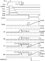
図3は、露光期間T_Eの全期間において転送トランジスタTXを中間電圧で駆動させた場合の画素回路GCのタイミングチャートである。なお、露光期間とは、被写体を露光する期間であり、PDは被写体からの信号電荷を蓄積する。図3に示すように画素回路GCは、露光期間T_Eと、読出期間T_Rとがサイクリックに繰り返され、露光期間T_Eにおいて蓄積した信号電荷に応じたシグナル信号を出力する。
露光期間T_Eでは、時刻t0に示すように、φTX=VMとされている。そのため、PDは高輝度光入射時にはサブスレショルド状態となり、FDに信号電荷を流しつつ信号電荷を蓄積する。これにより、リニアログ特性が実現される。
なお、露光期間T_Eでは、FDはRSTにより常時リセットされるため、PDから流れ出る信号電荷を絶えず排出し、信号電荷を蓄積しない。そのため、FDの電圧は絶えずPVDDを維持する。また、露光期間T_EではφVSEN=VLであるため、画素回路GCからカラムADC31にシグナル信号は出力されない。
露光期間T_Eが終了され、読出期間T_Rが開始されると、φRST=VLにされ、RSTはFDのリセットを終了し、φTX=VLにされ、TXは非導通状態となる。
時刻t1において、φVSEN=VHであり、SELが導通状態にされている。これにより、垂直信号線L_1からは、FDに現れるノイズレベルの電圧V_nがSFで電流増幅され、ノイズ信号としてカラムADC31に出力される。ここで、FDの電圧が、PVDDから電圧V_nに下がっているのは、主にφRSTをVHからVLに変化させたことによるFDとRSTとの間の寄生容量の影響によるものであるが、FDのktcノイズの影響も含まれている。このktcノイズは画素回路GC毎にばらついているため、ノイズ信号は画素回路GC毎にバラツキを持つ。なお、FDの電圧は、蓄積する信号電荷量が増大するにつれて低下する。
時刻t2において、φVSEN=VLであり、SELが非導通状態であり、ノイズ信号の出力が停止されている。また、時刻t2において、φTX=VHにされ、TXが導通状態となり、PDの信号電荷がFDに転送される。
これにより、FDの電圧はFDに転送される信号電荷に応じて低下し、シグナルレベルの電圧V_sとなる。
時刻t3において、φVSEN=VHであり、FDの電圧V_sがSFで電流増幅され、シグナル信号として、垂直信号線L_1を介してカラムADC31に出力されている。出力されたシグナル信号は、カラムADC31によりノイズ信号との差分がとられ、映像信号が生成される。ここで、映像信号は、FDのノイズレベルの電圧V_nと、シグナルレベルの電圧V_sとの差分に相当する値を有している。よって、ノイズ信号とシグナル信号との差分をとることで、シグナル信号に含まれるノイズ成分が除去された映像信号が得られるのである。
読出期間T_Rが終了すると、再度、φRST=VH、φVSEN=VL、φTX=VMとされ、次のフレームの映像信号を得るための露光期間T_Eが開始される。
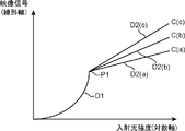
図4は、図3のタイミングチャートに従って駆動される画素回路GCの光電変換特性を示したグラフである。図4において、縦軸は線形軸であり画素回路GCから出力される映像信号を示し、横軸は対数軸であり、光電変換素子PDに入射する入射光の強度を示している。
このグラフから分かるように、光電変換特性は、変曲点P1を境に低輝度領域が線形(リニア)特性を示す線形特性部D1と、高輝度領域が対数(ログ)特性を示す対数特性部D2とからなるリニアログ特性を持つ。なお、図4のグラフにおいて、線形特性部D1がカーブを描いて上昇し、対数特性部D2がほぼ直線状に上昇しているのは、横軸を対数軸としたからである。
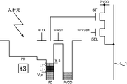
図5から図9は、図3の時刻t0から時刻t4に対応する画素回路GCのエネルギーバンド図である。図5~図9に示すエネルギーバンド図は、下側に向かうにつれて電圧が高いことを示している。
図5に示す時刻t0において、φRST=VHとされているため、FDはRSTによってリセットされ、PVDDの電圧を維持する。また、φTX=VMに設定されているため、PDとFDとの間にはエネルギー障壁ESが発生する。PDが蓄積する信号電荷量が一定の値未満の場合、PDに蓄積された信号電荷は、エネルギー障壁ESを乗り越えることができないため、PDからFDに移動できない。そのため、第1層L1の信号電荷は入射光量に対して線形特性となる。
一方、PDが蓄積する信号電荷量が一定の値以上になると、信号電荷はエネルギー障壁ESを乗り越えてPDからFDに移動することができる。これにより、PDはサブスレショルド状態となり、FDに信号電荷を漏らしつつ信号電荷を蓄積する。その結果、第2層L2の信号電荷は入射光量に対して対数特性となる。これにより、時刻t0に示す露光期間T_Eではリニアログ特性が実現される。
図6に示す時刻t1において、露光期間T_Eが終了したため、φTX=VLとされ、TXが非導通状態となる。そのため、エネルギー障壁ESが高くなり、信号電荷はPDからFDに移動することができなくなる。
時刻t1では、FDのリセットが終了しているため、主にφRSTをVHからVLに変化させたことによるFDとRSTとの間の寄生容量の影響によって、FDの電圧がPVDDから電圧V_nに低下している。そして、時刻t1では、φVSEN=VHとされ、電圧V_nがSFで電流増幅され、電流増幅された電圧V_nがSELを介して垂直信号線L_1からノイズ信号として出力される。
図7に示す時刻t2において、φTX=VHとされTXが導通状態とされる。これにより、エネルギー障壁ESが無くなり、PDからFDに信号電荷が転送される。そして、FDは第1層L1及び第2層L2からなる信号電荷を蓄積し、電圧が電圧V_nから電圧V_sに低下する。
図8に示す時刻t3において、φTX=VLとされTXが非導通状態とされる。そして、φVSEN=VHとされ、電圧V_sがSFにより電流増幅され、電流増幅された電圧V_sがSELを介して垂直信号線L_1からシグナル信号として出力される。
図9に示す時刻t4において、読出期間T_Rが終了して露光期間T_Eが開始されたため、φTX=VMとされ、TXが中間状態となって再度露光が行われている。また、時刻t4において、φRST=VHとされたため、FDの電圧が再度PVDDに上がっている。
図10は、図1に示すカラムADC31の回路図である。カラムADCは、上流側から順番に、CDS回路41、クランプ部42、比較部43、及びラッチ回路44を備えている。CDS回路41は、反転アンプ(以下、「AMP」と記述する。)、コンデンサCIN,CF、及びスイッチSW1を備えている。
AMPの入力ノードI_1はコンデンサCINを介して垂直信号線L_1と接続されている。AMPの入出力ノード間には、コンデンサCFが接続されている。コンデンサCFにはスイッチSW1が並列接続されている。コンデンサCINの垂直信号線L_1側の端子はノードVPIXである。
クランプ部42は、コンデンサC0及びスイッチSW2を備える。φCLがハイレベルになるとスイッチSW2がオンし、ノードBBの電圧がクランプ電圧VCLでクランプされる。
比較部43は、スイッチSW3,SW4,SW5,SW6、コンパレータCOMP1(以下、「COMP1」と記述する。)、コンパレータCOMP2(以下、「COMP2」と記述する。)、コンデンサC1,C2を備えている。
スイッチSW3は、ノードBB及びノードCC間に接続されている。スイッチSW4は一端がノードCCに接続され、他端がランプ信号(以下、「VRAMP」と記述する。)の電圧源に接続される。
COMP1は入力ノード(以下、「ノードDD」と記述する。)がコンデンサC1を介してノードCCに接続されている。COMP1の入出力ノード間にはスイッチSW5が接続されている。COMP1の出力ノードはコンデンサC2を介してCOMP2に接続されている。COMP2の入出力ノード間にはスイッチSW6が接続されている。COMP2の出力ノードは、インバータI1を介してラッチ回路44が接続されている。ラッチ回路44は、最上位ビットがD0、最下位ビットがD(n)のn+1ビットのデジタルの映像信号を保持する、n+1ビットのラッチ回路である。本実施の形態では、例えばn=13が採用され、ラッチ回路44は14ビットの映像信号を保持する。
図11は、図10に示すカラムADC31のタイミングチャートである。なお、図11に示す時刻t1,t3は図3の同時刻に対応している。
読出期間T_Rが開始されると、画素回路GCからノイズ信号が出力される。これにより、ノードVPIXの電圧はノイズレベルLV_nに上昇する(時刻t1)。なお、ノイズレベルLV_nの電圧はCDS回路41で保持される。
次に、φPRST,φCL,φS1,φS2がそれぞれ、一定時間、ハイレベルとなり、CDS回路41、クランプ部42、及びCOMP1,COMP2がそれぞれリセットされる。これにより、ノードAAの電圧はVTH(AMP)となり、ノードBB,CCの電圧はVCLとなり、ノードDDの電圧はVTH(COMP1)となる。
次に、画素回路GCからシグナル信号が出力されると、ノードVPIXの電圧がΔVだけ低下してシグナルレベルLV_sとなる(時刻t3)。
ノードVPIXのΔV分の電圧の低下に応じて、ノードAA,BB,CC,DDの電圧がそれぞれ上昇する。具体的には、ノードAA,BBはΔV×CIN/CF上昇する。ノードCC,DDはΔV×(CIN/CF)×C0/(C0+C1)上昇する。つまり、CDS回路41により、ノイズ信号とシグナル信号との差分がとられ、この差分を示すΔVに応じた電圧がノードAA~ノードDDに現れる。
次に、φSHがローレベル、φSHXがハイレベルとなり、スイッチSW3がオン、スイッチSW4がオフし、VRAMPの入力が開始される(時刻TT1)。
また、時刻TT1になると、カウンタ45のカウント動作が開始される。そして、時刻TT2において、ノードDDの電圧がVTH(COMP1)を超えると、COMP1の出力が反転し、その反転に応じて、インバータI1からの出力信号であるCOMPOUTが反転する。
COMPOUTが反転すると、ラッチ回路44はそのときのカウント値をラッチする。時刻TT1において、ノードCCの電圧は、ΔV×(CIN/CF)×C0/(C0+C1)から、VRAMPの入力開始時の電圧Va分低下するため、このときのノードCCのレベルはΔVに応じた値を持つ。したがって、時刻TT1~時刻TT2の期間はΔVに応じた値を持つ。そのため、VRAMPが入力されてから、COMPOUTが反転するまでの時間をカウントすることで、ΔVに応じたデジタル値、つまり、映像信号のデジタル値を得ることができる。
図12は、図2に示す画素回路GCにおいて感度を変えたときの光電変換特性を示したグラフである。図12において、縦軸は線形軸であり画素回路GCから出力される映像信号を示し、横軸は対数軸であり、光電変換素子PDに入射する入射光の強度を示している。
光電変換特性C(a)は図4に示す感度が標準に設定された画素回路GCの光電変換特性である。光電変換特性C(a)において、線形特性部D1(a)の感度を上げたい場合、例えば、i)カラムADC31のゲインを上げる、ii)カラムADC31の入力レンジを小さくする、iii)AD変換後の映像信号にデジタルゲインを加える等が考えられる。
ここで、i)を実現するには、図10に示すCIN/CFを増大させればよい。ii)を実現するには図11に示すVRAMPの振幅を小さくすればよい。VRAMPの振幅を小さくするには、Vb-Vaの差を小さくすればよい。iii)を実現するには、AD変換された映像信号を取り込んだ制御部14がデジタルの映像信号を所定倍(例えば2倍、3倍)すればよい。
例えば、光電変換特性C(a)に2倍のゲインを与えた場合を考える。この場合、光電変換特性C(b)が得られる。光電変換特性C(b)に示すように、単に光電変換特性C(a)に2倍のゲインを与えてしまうと、線形特性部D1(a)だけでなく対数特性部D2(a)の感度も上がってしまう。そのため、光電変換特性C(b)のダイナミックレンジDM(b)は光電変換特性C(a)のダイナミックレンジDM(a)よりも低下してしまう。
そこで、本実施の形態では、対数特性部D2の感度のみを可変にし、光電変換特性C(c)を得ている。光電変換特性C(c)では、線形特性部D1(c)の傾きは、線形特性部D1(a)の傾きの2倍になり、線形特性部D1(c)の感度が線形特性部D1(a)の2倍になっている。一方、対数特性部D2(c)の傾きは対数特性部D2(a)の傾きの1/2になり、対数特性部D2(c)の感度が対数特性部D2(a)の感度の1/2になっている。
そのため、光電変換特性C(c)のダイナミックレンジDM(c)が増大し、光電変換特性C(a)のダイナミックレンジDM(a)と同じになっている。これを実現するために、本実施の形態では、制御部14は、上述したように、φTX=VMの印加時間を変化させている。
図13は、本発明の実施の形態1におけるTXのタイミングチャートである。VDは1フレームの露光期間T_Eの開始タイミングを示している。(a)は感度を変化させない場合を示し、(b)は感度を(a)よりも低くした場合、(c)は感度を(b)よりも低くした場合を示している。なお、読出期間T_Rは露光期間T_Eよりも大幅に短いため、図13では、読出期間T_Rの図示を省略し、各フレームの露光期間T_Eを繋げて記載している。
図13(a)では、1フレームの露光期間T_Eにおいて、常にφTX=VMであり、TXのゲートには、常に中間電圧VMが印加される。
一方、図13(b)、(c)では、1フレームの露光期間T_Eの前半期間においてφTX=VLにされ、転送トランジスタTXのゲートは閉じられ、後半期間において、φTX=VMにされ、転送トランジスタTXのゲートは半開にされる。
図14は、図13(a)、(b)、(c)のφTXでTXを駆動させたときの画素回路GCの光電変換特性C(a)、C(b)、C(c)である。
図14に示すように、光電変換特性C(a)から光電変換特性C(c)の順で対数特性部D2(a)~(c)の傾きが減少し、感度が下がっていることが分かる。つまり、露光期間T_Eにおいて、φTX=VMの期間が長くなるにつれて、対数特性部D2の傾きが増大し、感度が上がっていることが分かる。
図15は、露光期間T_Eの前半期間をφTX=VLにし、後半期間をφTX=VMにしてTXを駆動した際の画素回路GCのタイミングチャートである。
露光期間T_Eの前半期間の時刻t0において、φTX=VLに設定され、TXのゲートが閉じられている。そのため、PDはリニア特性で信号電荷を蓄積する。
露光期間T_Eの後半期間の時刻t1において、φTX=VMに設定され、転送トランジスタTXのゲートが半開にされる。これにより、PDは信号電荷をリニアログ特性で蓄積する。図15の期間tint_logが後半期間であり、転送トランジスタTXのゲートが半開にされている。読出期間T_Rの動作は図3と同じである。
次の露光期間T_Eの前半期間の時刻t5において、φTX=VLにされ、TXのゲートが閉められる。これにより、露光期間T_Eの前半期間では、ゲートを閉めた状態でTXが駆動される。
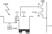
図16から図21は図15の時刻t0から時刻t5に対応する画素回路GCのエネルギーバンド図である。図16~図21に示すエネルギーバンド図は、下側に向かうにつれて電圧が高いことを示している。
以下、図16~図21を用いて、期間tint_logと対数特性部D2の感度との関係について説明する。
図16に示す時刻t0において、φTX=VLであり、TXのゲートが閉じられているため、PDとFDとの間には大きなエネルギー障壁ESが発生する。そのため、PDに蓄積された信号電荷はエネルギー障壁ESを乗り越えることができず、PDからFDに移動できない。よって、入射光量に対して線形特性である第1層L1のみからなる信号電荷がPDに蓄積される。この状態で、被写体の輝度が高い場合、PDは飽和状態となる。
図17に示す時刻t1において、φTX=VMであり、転送トランジスタTXのゲートが半開になる。これにより、エネルギー障壁ESが小さくなり、PDの上部に蓄積されていた信号電荷は、FDの方へ漏れ出ていく。
PDからFDへの信号電荷の漏れ出しは、瞬時に起こるわけではなく、一定時間を要し、時間応答性がある。そのため、期間tint_logの時間に応じて、露光期間T_Eの終了時に最終的にPDに残る信号電荷の量が異なってくる。ここで、期間tint_logが増大するほど、最終的にPDに残る対数特性の信号電荷の量が、本来、PDに蓄積されるべき対数特性の信号電荷の量に近づく。そのため、期間tint_logが長くなるにつれて、対数特性部D2の傾きが増大し、対数特性部D2の感度が高くなる。一方、期間tint_logが短くなるにつれて、最終的にPDに残る対数特性の信号電荷の量が、本来、PDに蓄積されるべき対数特性の信号電荷の量から離れる。そのため、期間tint_logが短くなるにつれて、対数特性部D2の傾きが減少し、対数特性部D2の感度が低くなる。
そこで、実施の形態1では、制御部14は、被写体の輝度を求め、被写体の輝度が高くなるにつれて期間tint_logを短くして、対数特性部D2の感度を低下させてダイナミックレンジを確保する。一方、制御部14は、被写体の輝度が低くなるにつれて期間tint_logを長くして、対数特性部D2の感度を上げている。
なお、制御部14は、被写体の輝度と期間tint_logとの関係を予め定めた関数やLUTを用いて、期間tint_logを求めればよい。そして、求めた期間tint_logでTXを駆動するための制御信号をTG6に出力すればよい。この制御信号を受けたTG6は、制御部14により求められた期間tint_logを持つφTXでTXが駆動されるようにローデコーダ2を制御すればよい。
ここで、制御部14は、画素アレイ部1を構成する全部又は一部の画素回路GCから出力される映像信号の平均値を被写体の輝度として算出すればよい。また、制御部14は、画素アレイ部1を構成する全部又は一部の画素回路GCから出力される映像信号のヒストグラムを求め、このヒストグラムの最大のピークを被写体の輝度として算出すればよい。
図18に示す時刻t2において、図6の時刻t1のときと同様、露光期間T_Eが終了したため、φTX=VLとされ、TXが非導通状態となる。そのため、エネルギー障壁ESが高くなり、信号電荷はPDからFDに移動することができなくなる。
図19に示す時刻t3において、図7に示す時刻t2と同様、φTX=VHとされ、TXが導通状態とされる。これにより、エネルギー障壁ESが無くなり、PDからFDに信号電荷が転送される。
図20に示す時刻t4において、図9に示す時刻t4と同様、φTX=VLとされTXが非導通状態とされる。そして、φVSEN=VHとされ、電圧V_sがSFにより電流増幅され、電流増幅された電圧V_sがSELを介して垂直信号線L_1からシグナル信号として出力される。
図21に示す時刻t5において、読出期間T_Rが終了して露光期間T_Eが開始されたため、φTX=VHとされ、TXが非導通状態となって再度露光が行われている。ここで、φTX=VHとされているため、φTX=VMとされた図9の時刻t4の場合と比べて、エネルギー障壁ESが高くなっていることが分かる。
このように、本実施の形態では、露光期間T_Eの前半期間はφTX=VLとされ、露光期間T_Eの後半期間はφTX=VMとされる。そして、被写体の輝度が高いときは期間tint_logが短くされてダイナミックレンジが確保される。一方、被写体の輝度が低いときは、期間tint_logが長くされて感度が高くされる。そのため、感度の上昇とダイナミックレンジの確保との両立を図ることができる。
(実施の形態2)
次に、実施の形態2の固体撮像装置について説明する。実施の形態2の固体撮像装置は、露光期間T_Eに中間電圧(以下、「VM1」と記述する。)及び中間電圧(以下、「VM2」と記述する。)を印加したことを特徴とする。なお、本実施の形態において、実施の形態1と同一のものは説明を省略する。
次に、実施の形態2の固体撮像装置について説明する。実施の形態2の固体撮像装置は、露光期間T_Eに中間電圧(以下、「VM1」と記述する。)及び中間電圧(以下、「VM2」と記述する。)を印加したことを特徴とする。なお、本実施の形態において、実施の形態1と同一のものは説明を省略する。
図22は、本発明の実施の形態2におけるTXのタイミングチャートである。(a)は感度を変化させない場合を示し、(b)は感度を(a)よりも高くした場合、(c)は感度を(b)よりも高くした場合を示している。なお、読出期間T_Rは露光期間T_Eよりも大幅に短いため、図22では、読出期間T_Rの図示を省略し、各フレームの露光期間T_Eを繋げて記載している。
(a)では、1フレームの露光期間T_Eにおいて、常にφTX=VM2であり、転送トランジスタTXのゲートには、常にVM2が印加される。
一方、図22の(b)、(c)では、1フレームの露光期間T_Eの前半期間においてφTX=VM1にされ、後半期間においてφTX=VM2にされている。
ここで、VM1<VM2である。そのため、前半期間、後半期間ともTXのゲートは半開にされているが、後半期間の方が前半期間よりもゲートが大きく開いている。なお、VM2は、画素回路GCの光電変換特性の変曲点P1を目的の値にするための中間電圧である。
図23は、図22(a)、(b)、(c)のφTXでTXを駆動させたときの画素回路GCの光電変換特性C(a)、C(b)、C(c)である。
図23に示すように、光電変換特性C(a)から光電変換特性C(c)の順で対数特性部D2(a)~D2(c)の傾き増大し、感度が上がっていることが分かる。つまり、露光期間T_Eにおいて、φTX=VM2の期間が短くなるにつれて、対数特性部D2の傾きが増大し、感度が上がっていることが分かる。
図24は、露光期間T_Eの前半期間をφTX=VM1にし、後半期間をφTX=VM2にしてTXを駆動した際の画素回路GCのタイミングチャートである。
露光期間T_Eの前半期間の時刻t0において、φTX=VM1に設定され、TXのゲートが半開にされている。そのため、PDはリニアログ特性で信号電荷を蓄積する。
露光期間の後半期間の時刻t1において、φTX=VM2に設定され、TXのゲートが前半期間よりも更に開いた状態で半開にされる。これにより、PDは信号電荷をリニアログ特性で蓄積する。図24の期間tlog_secが後半期間である。読出期間T_Rの動作は図3と同じである。
次の露光期間T_Eの前半期間の時刻t5において、φTX=VM1にされ、TXのゲートが半開にされる。これにより、露光期間T_Eの前半期間では、ゲートが半開された状態でTXが駆動される。
図25、図26は図24の時刻t0,時刻t1に対応する画素回路GCのエネルギーバンド図である。図25、図26に示すエネルギーバンド図は、下側に向かうにつれて電圧が高いことを示している。なお、図24に示す時刻t2,t3,t4のエネルギーバンド図は、実施の形態1と同一であるため説明を省く。
以下、図25、図26を用いて、期間tlog_secと対数特性部D2の感度との関係について説明する。
図25に示す時刻t0において、φTX=VM1であり、TXのゲートが半開とされ、PDとFDとの間にエネルギー障壁ESが発生している。この状態では、被写体の輝度が高い場合は、PDはVM1で定まるサブスレショルド状態となり、リニアログ特性で信号電荷を蓄積する。また、この状態では、PDはVM1より下の第1層L1に属する信号電荷を線形特性で蓄積し、VM1より上側の第2層L2に属する信号電荷を対数特性で蓄積している。
図26に示す時刻t1において、φTX=VM2であり、TXのゲートが時刻t0のときよりも更に開いた半開状態にされる。これにより、エネルギー障壁ESは時刻t0のときよりも低くなる。
この状態になると、VM2よりも上側の層に属する信号電荷は、FDの方へ漏れ出していくが、この信号電荷の漏れ出しは瞬時に起こるわけではなく、ある程度の時間応答性を有している。
そのため、期間tlog_secが短いと、第2層L2に属する信号電荷は、VM1及びVM2間の層L1´に蓄積されている信号電荷の上にのることになる。この層L1´に属する信号電荷は時刻t0において第1層L1に属していた信号電荷である。
期間tlog_secが長くなるにつれて、層L1´の信号電荷はFD側に漏れ出して層L1´は対数特性になっていき、第2層L2に吸収され、やがて消滅するが、期間tlog_secが短ければ、対数特性のようにふるまって第2層L2のオフセットとなる。そのため、期間tlog_secが短ければ、露光期間T_Eの終了時において、PDに残存する信号電荷のうち、対数特性で蓄積された信号電荷の成分が増し、対数特性部D2の感度が高くなるのである。
また、VM1とVM2との差が大きい場合も、同様に、対数特性部D2の感度を高くすることができる。つまり、VM1とVM2との差が大きければ、それだけ、層L1´の高さが増すため、第2層L2のオフセットが増える。よって、露光期間T_Eの終了時において、PDに残存する信号電荷のうち、対数特性で蓄積された信号電荷の成分が増し、対数特性部D2の感度が高くなるのである。
以上のことから、対数特性部D2の感度は、期間tlog_secの長さと、VM2及びVM1の電圧差とに依存するのである。
そこで、制御部14は、実施の形態1と同様にして被写体の輝度を求め、被写体の輝度が高くなるにつれて、期間tlog_secを長くする制御、並びにVM1を上げてVM1及びVM2の電圧差を小さくする制御の少なくともいずれか一方を実行することで、対数特性部D2の感度を下げ、ダイナミックレンジを確保する。
一方、制御部14は、被写体の輝度が低くなるにつれて、期間tlog_secを短くする制御、並びにVM1を下げてVM1及びVM2の電圧差を大きくする制御の少なくともいずれか一方を実行することで、対数特性部D2の感度を上げている。
ここで、制御部14は、被写体の輝度と期間tlog_secとの関係を予め定めた関数やLUTを用いて、期間tlog_secを求めればよい。又は、被写体の輝度と期間VM1との関係を予め定めた関数やLUTを用いて、VM1を求めればよい。そして、求めた期間tlog_sec又はVM1でTXを駆動するための制御信号をTG6に出力すればよい。この制御信号を受けたTG6は、制御部14により求められた期間tlog_sec,VM1を持つφTXでTXが駆動されるようにローデコーダ2を制御すればよい。
なお、実施の形態2において、露光期間T_Eを3つの期間に分け、1つ目の期間をφTX=VL、2つ目の期間をφTX=VM1、3つ目の期間をφTX=VM2にしてもよい。φTX=VLの期間を設けることで、TXの暗電流に起因する信号電荷がFDに蓄積されることを防止することができる。
このように、実施の形態2では、露光期間T_Eにおいて、φTX=VM1とした後、φTX=VM2とし、被写体の輝度に応じてVM2を印加する期間を変える制御、並びにVM1及びVM2の電圧差を変える制御の少なくともいずれか一方が行われている。そのため、感度の増大とダイナミックレンジの確保との両立を図ることができる。
(実施の形態3)
実施の形態3は、明るい被写体の存在の有無を判定し、実施の形態1の手法を用いて、明るい被写体が存在する場合は感度を下げる制御を行い、明るい被写体が存在しない場合は感度を上げる制御を行うことを特徴としている。
実施の形態3は、明るい被写体の存在の有無を判定し、実施の形態1の手法を用いて、明るい被写体が存在する場合は感度を下げる制御を行い、明るい被写体が存在しない場合は感度を上げる制御を行うことを特徴としている。
なお、本実施の形態において、実施の形態1、2と同じものは説明を省略する。本実施の形態では、制御部14は、明るい被写体が存在すると判定した場合、明るい被写体が存在しないと判定した場合に比べて、期間tint_logを短くする。これにより、対数特性部D2の感度が低くなり、ダイナミックレンジが確保される。
一方、制御部14は、明るい被写体が存在しないと判定した場合、明るい被写体が存在すると判定した場合に比べて、期間tint_logを長くする。これにより、対数特性部D2の感度が高くなる。
具体的には、制御部14は、明るい被写体が存在すると判定した場合、期間tint_logを、明るい被写体が存在する場合において予め定められた期間T_downに設定する。一方、制御部14は、明るい被写体が存在しないと判定した場合、期間tint_logを、明るい被写体が存在しない場合において予め定められた期間T_upに設定すればよい。ここで、期間T_up>期間T_downである。そのため、明るい被写体が存在する場合は、期間tint_logが短くなり、感度を下げてダイナミックレンジを確保し、明るい被写体が存在しない場合は、期間tint_logが長くなり、感度を上げることができる。
なお、制御部14は、明るい被写体が存在しないと判定した場合、露光期間T_Eの全期間を期間tint_logとしてもよい。こうすることで、明るい被写体が存在しない場合の感度を最大限に高めることができる。
ここで、制御部14は、各画素回路GCから出力される映像信号の平均値に基づいて、明るい被写体の存在の有無を判定すればよい。
具体的には、制御部14は、画素アレイ部1を構成する全部又は一部の画素回路GCから出力される映像信号の平均値を求め、この平均値を規定値V_th1と比較し、平均値が規定値V_th1以上の場合、明るい被写体が存在すると判定し、平均値が規定値V_th1未満の場合、明るい被写体が存在していないと判定すればよい。
規定値V_th1としては、図4に示す対数特性部D2の高輝度側の所定のレベルを採用すればよい。
また、制御部14は、画素アレイ部1を構成する全部又は一部の画素回路GCから出力される映像信号のヒストグラムを求め、このヒストグラムに基づいて、被写体が明るいか否かを判定してもよい。この場合、制御部14は、横軸に映像信号の階調値、縦軸に頻度を規定する映像信号のヒストグラムのグラフを求め、このグラフから最も高階調側にあるピークを特定し、そのピークの階調値が規定値V_th2以上であれば、被写体が明るいと判定し、そのピークの階調値が規定値V_th2未満であれば、被写体が暗いと判定すればよい。
規定値V_th2としては、図4に示す規定値V_th1を採用してもよいし、規定値V_th1よりも多少低い値を採用してもよいし、規定値V_th1よりも多少高い値を採用してもよい。
また、制御部14は、ヒストグラムにおいて、規定値V_th1よりも高い階調値の頻度の合計値を求め、この合計値が規定値V_th3以上であれば、明るい被写体が存在すると判定し、この合計値が規定値Vth_3未満であれば、明るい被写体が存在しないと判定してもよい。ここで、規定値V_th3としては、例えば、画素アレイ部1を構成する全画素回路GCの個数に対して、規定値V_th1以上の階調値の映像信号を出力した画素回路GCの個数が所定の割合(例えば、90%、80%)となるような値を採用すればよい。
このように、本実施の形態では、明るい被写体が存在する場合はダイナミックレンジを確保し、明るい被写体が存在しない場合は感度を上げることができる。
(実施の形態4)
実施の形態4は、明るい被写体の存在の有無を判定し、実施の形態2の手法を用いて、明るい被写体が存在する場合は感度を下げる制御を行い、明るい被写体が存在しない場合は感度を上げる制御を行うことを特徴としている。なお、本実施の形態において、実施の形態1~3と同一のものは説明を省略する。
実施の形態4は、明るい被写体の存在の有無を判定し、実施の形態2の手法を用いて、明るい被写体が存在する場合は感度を下げる制御を行い、明るい被写体が存在しない場合は感度を上げる制御を行うことを特徴としている。なお、本実施の形態において、実施の形態1~3と同一のものは説明を省略する。
本実施の形態において、制御部14は、実施の形態3と同じ手法を用いて明るい被写体の存在の有無を判定する。そして、制御部14は、明るい被写体の存在の有無を判定し、明るい被写体が存在すると判定した場合、明るい被写体が存在しないと判定した場合に比べて、期間tlog_secを長くする。
具体的には、制御部14は、明るい被写体が存在すると判定した場合、期間tlog_secを所定の期間T_upに設定する。一方、制御部14は、明るい被写体が存在しないと判定した場合、期間tlog_secを所定の期間T_downに設定する。ここで、期間T_up>期間T_downである。
よって、明るい被写体が存在する場合、期間tlog_secが期間T_upに設定されて、φTX=VM2の期間が増大し、対数特性部D2の感度が下がる。一方、明るい被写体が存在しない場合、期間tlog_secが期間T_downに設定され、φTX=VM2の期間が減少し、対数特性部D2の感度が上がる。
なお、制御部14は、明るい被写体が存在すると判定した場合、VM1及びVM2の電圧差を、明るい被写体が存在しないと判定した場合に比べて小さくしてもよい。一方、制御部14は、明るい被写体が存在しないと判定した場合、VM1及びVM2の電圧差を、明るい被写体が存在すると判定した場合に比べて大きくしてもよい。具体的には、変曲点P1を所望の値にするためにVM2は固定とされているので、明るい被写体が存在する場合は、VM1の値を明るい被写体が存在しない場合に比べて大きな値VM1_bigに設定し、VM1及びVM2の電圧差を小さくすればよい。一方、明るい被写体が存在しない場合は、VM1の値を値VM1_smallに設定し、VM1及びVM2の電圧差を大きくすればよい。なお、値VM1_bigとしては、ダイナミックレンジを確保する上で予め定められた好適な値を採用すればよい。また、値VM1_smallとしては、対数特性部D2の感度を上げるうえで予め定められた好適な値を採用すればよい。
なお、本実施の形態において、期間tlog_secを変える制御とVM1及びVM2の電圧差を変える制御とを組み合わせても良い。
このように、本実施の形態によれば、実施の形態3と同様の効果を得ることができる。
上述した固体撮像装置の技術的特徴は下記のようにまとめることができる。
(1)本発明による固体撮像装置は、低輝度側が線形特性を示す線形特性部と、高輝度側が対数特性を示す対数特性部とを備えるリニアログ特性を持つ画素回路を備える固体撮像装置であって、前記画素回路は、入射光量に応じた信号電荷を蓄積するフォトダイオードと、浮遊拡散層と、前記フォトダイオードに蓄積された信号電荷を前記浮遊拡散層に転送する転送トランジスタとを備え、被写体を露光する露光期間において複数の電圧を前記転送トランジスタのゲートに印加することで、前記対数特性部の感度を変化させる制御部を備える。
この構成によれば、露光期間中に複数種類の電圧が転送トランジスタのゲートに印加されている。そのため、線形特性部の感度は維持させて、対数特性部の感度のみを制御することができる。そのため、被写体の輝度が高い場合は、対数特性部の感度を下げて画素回路のダイナミックレンジを確保し、被写体の感度が低い場合は、対数特性部の感度を上げることができる。
(2)前記制御部は、前記露光期間の少なくとも最後の期間において、前記転送トランジスタのゲートに中間電圧を印加して前記ゲートを半開させ、前記中間電圧を印加する期間を変えることで前記対数特性部の感度を変化させることが好ましい。
この構成によれば、露光期間の少なくとも最後の期間において、転送トランジスタのゲートに中間電圧が印加されてゲートが半開にされる。そして、中間電圧を印加する期間を変えることで対数特性部の感度が変化されている。ここで、露光期間において、中間電圧を印加する期間が長くなると、露光期間の終了時において、光電変換素子に最終的に残存している信号電荷は本来持つべき対数特性の信号電荷の量に近づくことになる。そのため、中間電圧を印加する期間を長くすることで、対数特性部の感度を上げることができる。
なお、少なくとも最後の期間とは、露光期間を複数の期間に区分した場合の最後の期間を指している。例えば、露光期間を前半期間と後半期間との2つの期間に区分した場合は後半期間が少なくとも最後の期間に該当することになる。
(3)前記制御部は、前記露光期間を2つの期間に分け、前半期間において前記ゲートを閉める電圧を前記ゲートに印加し、後半期間において前記中間電圧を前記ゲートに印加することが好ましい。
この構成によれば、露光期間の前半期間において転送トランジスタのゲートが閉められているため、転送トランジスタのゲートの電極下部の基板層と絶縁層との界面で発生する暗電流を抑制することができる。
(4)前記制御部は、前記露光期間において、前記ゲートに第1中間電圧を印加して前記ゲートを半開させた後、前記ゲートに第1中間電圧よりも大きい第2中間電圧を印加して前記ゲートを更に開き、前記第2中間電圧を印加する期間を変える制御並びに第1中間電圧及び第2中間電圧の電圧差を変える制御の少なくとも一方を行うことで、前記対数特性部の感度を変化させることが好ましい。
この構成によれば、露光期間の途中で第1中間電圧から第2中間電圧に切り替えられるため、ゲートが更に開いた状態にされる。そのため、露光期間の終了時において、光電変換素子に残存する信号電荷のうち、対数特性の信号電荷の成分を増大させることができ、対数特性部の感度を上げることができる。
ここで、第2中間電圧を印加する期間を短くする、又は第1中間電圧及び第2中間電圧の電圧差を大きくすると、対数特性の信号電荷の成分を増大させ、対数特性部の感度を上げることができる。一方、第2中間電圧を印加する期間を長くする、又は前記電圧差を小さくすると、対数特性の信号電荷の成分を減少させ、対数特性部の感度を下げることができる。したがって、第2中間電圧を印加する時間を変える制御及び電圧差を変える制御の少なくとも一方を行うことで、対数特性部の感度を変化させることができる。
(5)前記制御部は、明るい被写体の存在の有無を判定し、前記明るい被写体が存在すると判定した場合、前記明るい被写体が存在しないと判定した場合に比べて、前記中間電圧を印加する期間を短くすることが好ましい。
この構成によれば、明るい被写体が存在する場合は、中間電圧を印加する期間が短くされるため、対数特性部の感度が下がり、ダイナミックレンジを確保することができる。一方、明るい被写体が存在しない場合は、中間電圧を印加する期間が長くされるため、対数特性部の感度を上げることができる。
(6)前記制御部は、明るい被写体の存在の有無を判定し、前記明るい被写体が存在すると判定した場合、前記明るい被写体が存在しないと判定した場合に比べて前記第2中間電圧を印加する期間を長くする制御、並びに前記明るい被写体が存在しないと判定した場合に比べて前記電圧差を小さくする制御の少なくともいずれか一方を行うことが好ましい。
この構成によれば、明るい被写体が存在する場合は、明るい被写体が存在しない場合に比べて第2中間電圧を印加する期間が短くされる制御、又は、電圧差が小さくされる制御の少なくともいずれか一方が行われるため、対数特性部の感度が下がり、ダイナミックレンジを確保することができる。一方、明るい被写体が存在しない場合は、明るい被写体が存在する場合に比べて第2中間電圧を印加する期間が長くされる制御、又は、電圧差が大きくされる制御の少なくともいずれか一方が行われるため、対数特性部の感度を上げることができる。
(7)前記画素回路は、複数存在し、前記制御部は、各画素回路から出力される画素信号の平均値に基づいて、前記明るい被写体の存在の有無を判定することが好ましい。
この構成によれば、明るい被写体の存在の有無を精度良く判定することができる。
(8)前記画素回路は、複数存在し、前記制御部は、各画素回路から出力される画素信号のヒストグラムに基づいて、前記明るい被写体の存在の有無を判定することが好ましい。
この構成によれば、明るい被写体の存在の有無を精度良く判定することができる。
Claims (8)
- 低輝度側が線形特性を示す線形特性部と、高輝度側が対数特性を示す対数特性部とを備えるリニアログ特性を持つ画素回路を備える固体撮像装置であって、
前記画素回路は、入射光量に応じた信号電荷を蓄積するフォトダイオードと、浮遊拡散層と、前記フォトダイオードに蓄積された信号電荷を前記浮遊拡散層に転送する転送トランジスタとを備え、
被写体を露光する露光期間において複数の電圧を前記転送トランジスタのゲートに印加することで、前記対数特性部の感度を変化させる制御部を備える固体撮像装置。 - 前記制御部は、前記露光期間の少なくとも最後の期間において、前記転送トランジスタのゲートに中間電圧を印加して前記ゲートを半開させ、前記中間電圧を印加する期間を変えることで前記対数特性部の感度を変化させる請求項1記載の固体撮像装置。
- 前記制御部は、前記露光期間を2つの期間に分け、前半期間において前記ゲートを閉める電圧を前記ゲートに印加し、後半期間において前記中間電圧を前記ゲートに印加する請求項2記載の固体撮像装置。
- 前記制御部は、前記露光期間において、前記ゲートに第1中間電圧を印加して前記ゲートを半開させた後、前記ゲートに第1中間電圧よりも大きい第2中間電圧を印加して前記ゲートを更に開き、前記第2中間電圧を印加する期間を変える制御並びに第1中間電圧及び第2中間電圧の電圧差を変える制御の少なくとも一方を行うことで、前記対数特性部の感度を変化させる請求項1記載の固体撮像装置。
- 前記制御部は、明るい被写体の存在の有無を判定し、前記明るい被写体が存在すると判定した場合、前記明るい被写体が存在しないと判定した場合に比べて、前記中間電圧を印加する期間を短くする請求項2又は3記載の固体撮像装置。
- 前記制御部は、明るい被写体の存在の有無を判定し、前記明るい被写体が存在すると判定した場合、前記明るい被写体が存在しないと判定した場合に比べて前記第2中間電圧を印加する期間を長くする制御、並びに前記明るい被写体が存在しないと判定した場合に比べて前記電圧差を小さくする制御の少なくともいずれか一方を行う請求項4記載の固体撮像装置。
- 前記画素回路は、複数存在し、
前記制御部は、各画素回路から出力される画素信号の平均値に基づいて、前記明るい被写体の存在の有無を判定する請求項5又は6記載の固体撮像装置。 - 前記画素回路は、複数存在し、
前記制御部は、各画素回路から出力される画素信号のヒストグラムに基づいて、前記明るい被写体の存在の有無を判定する請求項5又は6記載の固体撮像装置。
Priority Applications (1)
| Application Number | Priority Date | Filing Date | Title |
|---|---|---|---|
| JP2012546680A JPWO2012073448A1 (ja) | 2010-11-29 | 2011-11-21 | 固体撮像装置 |
Applications Claiming Priority (2)
| Application Number | Priority Date | Filing Date | Title |
|---|---|---|---|
| JP2010265523 | 2010-11-29 | ||
| JP2010-265523 | 2010-11-29 |
Publications (1)
| Publication Number | Publication Date |
|---|---|
| WO2012073448A1 true WO2012073448A1 (ja) | 2012-06-07 |
Family
ID=46171422
Family Applications (1)
| Application Number | Title | Priority Date | Filing Date |
|---|---|---|---|
| PCT/JP2011/006457 Ceased WO2012073448A1 (ja) | 2010-11-29 | 2011-11-21 | 固体撮像装置 |
Country Status (2)
| Country | Link |
|---|---|
| JP (1) | JPWO2012073448A1 (ja) |
| WO (1) | WO2012073448A1 (ja) |
Cited By (2)
| Publication number | Priority date | Publication date | Assignee | Title |
|---|---|---|---|---|
| CN106851139A (zh) * | 2015-12-03 | 2017-06-13 | 豪威科技股份有限公司 | 用于全局快门校正的像素电路及成像系统 |
| US10321080B2 (en) | 2016-03-25 | 2019-06-11 | SK Hynix Inc. | Pixel output level control device and CMOS image sensor using the same |
Citations (3)
| Publication number | Priority date | Publication date | Assignee | Title |
|---|---|---|---|---|
| JP2006025122A (ja) * | 2004-07-07 | 2006-01-26 | Konica Minolta Holdings Inc | 撮像装置 |
| JP2008228058A (ja) * | 2007-03-14 | 2008-09-25 | Sony Corp | 撮像装置、撮像方法、露光制御方法、プログラム |
| JP2008306439A (ja) * | 2007-06-07 | 2008-12-18 | Konica Minolta Holdings Inc | 撮像素子および撮像装置 |
-
2011
- 2011-11-21 WO PCT/JP2011/006457 patent/WO2012073448A1/ja not_active Ceased
- 2011-11-21 JP JP2012546680A patent/JPWO2012073448A1/ja active Pending
Patent Citations (3)
| Publication number | Priority date | Publication date | Assignee | Title |
|---|---|---|---|---|
| JP2006025122A (ja) * | 2004-07-07 | 2006-01-26 | Konica Minolta Holdings Inc | 撮像装置 |
| JP2008228058A (ja) * | 2007-03-14 | 2008-09-25 | Sony Corp | 撮像装置、撮像方法、露光制御方法、プログラム |
| JP2008306439A (ja) * | 2007-06-07 | 2008-12-18 | Konica Minolta Holdings Inc | 撮像素子および撮像装置 |
Cited By (2)
| Publication number | Priority date | Publication date | Assignee | Title |
|---|---|---|---|---|
| CN106851139A (zh) * | 2015-12-03 | 2017-06-13 | 豪威科技股份有限公司 | 用于全局快门校正的像素电路及成像系统 |
| US10321080B2 (en) | 2016-03-25 | 2019-06-11 | SK Hynix Inc. | Pixel output level control device and CMOS image sensor using the same |
Also Published As
| Publication number | Publication date |
|---|---|
| JPWO2012073448A1 (ja) | 2014-05-19 |
Similar Documents
| Publication | Publication Date | Title |
|---|---|---|
| US20120305751A1 (en) | Solid-State Image Capture Device | |
| US7586523B2 (en) | Amplification-type CMOS image sensor of wide dynamic range | |
| US8659693B2 (en) | Solid-state image pickup element and camera system | |
| US10104326B2 (en) | Imaging apparatus including analog-to-digital conversion circuits to convert analog signals into digital signals, imaging system including analog-to-digital conversion circuits to convert analog signals into digital signals, and imaging apparatus driving method | |
| JP4798320B2 (ja) | 固体撮像装置 | |
| US7969484B2 (en) | Solid-state image sensing device | |
| US8508629B2 (en) | Analog row black level calibration for CMOS image sensor | |
| US7616146B2 (en) | A/D conversion circuit, control method thereof, solid-state imaging device, and imaging apparatus | |
| US8310580B2 (en) | Solid-state imaging device and camera system for suppressing occurrence of quantization vertical streaks | |
| US7733402B2 (en) | CMOS image sensor having wide dynamic range | |
| KR101614162B1 (ko) | 고체 촬상 센서 및 카메라 시스템 | |
| CN108605105B (zh) | 固体摄像装置以及摄像装置 | |
| JP2013098598A (ja) | 撮像装置 | |
| JP2012124835A (ja) | 固体撮像装置 | |
| WO2012056630A1 (ja) | 固体撮像装置 | |
| JP2012119775A (ja) | 固体撮像装置 | |
| WO2012073448A1 (ja) | 固体撮像装置 | |
| JP2013058960A (ja) | 固体撮像装置 | |
| JP2010226679A (ja) | 固体撮像装置 |
Legal Events
| Date | Code | Title | Description |
|---|---|---|---|
| 121 | Ep: the epo has been informed by wipo that ep was designated in this application |
Ref document number: 11845703 Country of ref document: EP Kind code of ref document: A1 |
|
| ENP | Entry into the national phase |
Ref document number: 2012546680 Country of ref document: JP Kind code of ref document: A |
|
| NENP | Non-entry into the national phase |
Ref country code: DE |
|
| 122 | Ep: pct application non-entry in european phase |
Ref document number: 11845703 Country of ref document: EP Kind code of ref document: A1 |