WO2012060096A1 - Photoelectric conversion element - Google Patents
Photoelectric conversion element Download PDFInfo
- Publication number
- WO2012060096A1 WO2012060096A1 PCT/JP2011/006123 JP2011006123W WO2012060096A1 WO 2012060096 A1 WO2012060096 A1 WO 2012060096A1 JP 2011006123 W JP2011006123 W JP 2011006123W WO 2012060096 A1 WO2012060096 A1 WO 2012060096A1
- Authority
- WO
- WIPO (PCT)
- Prior art keywords
- photoelectric conversion
- layer
- transition metal
- thin film
- conversion element
- Prior art date
Links
- 238000006243 chemical reaction Methods 0.000 title claims abstract description 108
- 229910052723 transition metal Inorganic materials 0.000 claims abstract description 67
- 150000003624 transition metals Chemical class 0.000 claims abstract description 55
- 239000010409 thin film Substances 0.000 claims abstract description 52
- 239000000758 substrate Substances 0.000 claims abstract description 51
- 239000013081 microcrystal Substances 0.000 claims abstract description 49
- 239000004065 semiconductor Substances 0.000 claims abstract description 12
- 150000001875 compounds Chemical class 0.000 claims abstract description 10
- 239000010410 layer Substances 0.000 claims description 210
- 239000010408 film Substances 0.000 claims description 55
- 239000000463 material Substances 0.000 claims description 19
- 229910016001 MoSe Inorganic materials 0.000 claims description 18
- 239000013078 crystal Substances 0.000 claims description 12
- 229910018072 Al 2 O 3 Inorganic materials 0.000 claims description 8
- 229910052738 indium Inorganic materials 0.000 claims description 8
- 239000002344 surface layer Substances 0.000 claims description 8
- 229910052733 gallium Inorganic materials 0.000 claims description 7
- 229910052782 aluminium Inorganic materials 0.000 claims description 5
- 239000002131 composite material Substances 0.000 claims description 3
- 238000007740 vapor deposition Methods 0.000 abstract description 14
- 238000000034 method Methods 0.000 description 64
- 238000004544 sputter deposition Methods 0.000 description 15
- 230000008569 process Effects 0.000 description 11
- 230000015572 biosynthetic process Effects 0.000 description 9
- 230000000052 comparative effect Effects 0.000 description 9
- 238000004519 manufacturing process Methods 0.000 description 9
- 238000003917 TEM image Methods 0.000 description 8
- 238000000605 extraction Methods 0.000 description 8
- IJGRMHOSHXDMSA-UHFFFAOYSA-N Atomic nitrogen Chemical compound N#N IJGRMHOSHXDMSA-UHFFFAOYSA-N 0.000 description 6
- 238000012360 testing method Methods 0.000 description 6
- 239000010407 anodic oxide Substances 0.000 description 5
- 230000006872 improvement Effects 0.000 description 5
- 229910052760 oxygen Inorganic materials 0.000 description 5
- 230000009467 reduction Effects 0.000 description 5
- 229910052711 selenium Inorganic materials 0.000 description 5
- 229910052717 sulfur Inorganic materials 0.000 description 5
- 238000000224 chemical solution deposition Methods 0.000 description 4
- 239000010419 fine particle Substances 0.000 description 4
- 239000005361 soda-lime glass Substances 0.000 description 4
- 238000004804 winding Methods 0.000 description 4
- QVGXLLKOCUKJST-UHFFFAOYSA-N atomic oxygen Chemical compound [O] QVGXLLKOCUKJST-UHFFFAOYSA-N 0.000 description 3
- 229910052798 chalcogen Inorganic materials 0.000 description 3
- 150000001787 chalcogens Chemical class 0.000 description 3
- 238000010586 diagram Methods 0.000 description 3
- 238000001704 evaporation Methods 0.000 description 3
- 239000000203 mixture Substances 0.000 description 3
- 229910052757 nitrogen Inorganic materials 0.000 description 3
- 239000001301 oxygen Substances 0.000 description 3
- 238000012545 processing Methods 0.000 description 3
- 238000005096 rolling process Methods 0.000 description 3
- CSCPPACGZOOCGX-UHFFFAOYSA-N Acetone Chemical compound CC(C)=O CSCPPACGZOOCGX-UHFFFAOYSA-N 0.000 description 2
- LFQSCWFLJHTTHZ-UHFFFAOYSA-N Ethanol Chemical compound CCO LFQSCWFLJHTTHZ-UHFFFAOYSA-N 0.000 description 2
- 238000002048 anodisation reaction Methods 0.000 description 2
- 150000004770 chalcogenides Chemical class 0.000 description 2
- 229910052804 chromium Inorganic materials 0.000 description 2
- 229910052802 copper Inorganic materials 0.000 description 2
- 230000032798 delamination Effects 0.000 description 2
- 230000000694 effects Effects 0.000 description 2
- 239000000284 extract Substances 0.000 description 2
- 239000007789 gas Substances 0.000 description 2
- 239000007791 liquid phase Substances 0.000 description 2
- 238000009832 plasma treatment Methods 0.000 description 2
- 238000004627 transmission electron microscopy Methods 0.000 description 2
- 229910001218 Gallium arsenide Inorganic materials 0.000 description 1
- 238000005411 Van der Waals force Methods 0.000 description 1
- 238000002441 X-ray diffraction Methods 0.000 description 1
- 229910021417 amorphous silicon Inorganic materials 0.000 description 1
- 238000007743 anodising Methods 0.000 description 1
- 230000008901 benefit Effects 0.000 description 1
- 230000005540 biological transmission Effects 0.000 description 1
- 238000004140 cleaning Methods 0.000 description 1
- 238000010549 co-Evaporation Methods 0.000 description 1
- 239000000470 constituent Substances 0.000 description 1
- 239000006059 cover glass Substances 0.000 description 1
- 238000005520 cutting process Methods 0.000 description 1
- 230000002950 deficient Effects 0.000 description 1
- 239000003792 electrolyte Substances 0.000 description 1
- 238000010894 electron beam technology Methods 0.000 description 1
- 238000011156 evaluation Methods 0.000 description 1
- 230000008020 evaporation Effects 0.000 description 1
- 238000009499 grossing Methods 0.000 description 1
- 230000010354 integration Effects 0.000 description 1
- 229910052742 iron Inorganic materials 0.000 description 1
- 238000005259 measurement Methods 0.000 description 1
- 238000000691 measurement method Methods 0.000 description 1
- 229910052750 molybdenum Inorganic materials 0.000 description 1
- 229910021421 monocrystalline silicon Inorganic materials 0.000 description 1
- 238000005121 nitriding Methods 0.000 description 1
- 230000001590 oxidative effect Effects 0.000 description 1
- 239000002245 particle Substances 0.000 description 1
- 238000000059 patterning Methods 0.000 description 1
- 239000012071 phase Substances 0.000 description 1
- 230000001443 photoexcitation Effects 0.000 description 1
- 238000005498 polishing Methods 0.000 description 1
- 229910021420 polycrystalline silicon Inorganic materials 0.000 description 1
- 230000001681 protective effect Effects 0.000 description 1
- 238000001552 radio frequency sputter deposition Methods 0.000 description 1
- 238000012827 research and development Methods 0.000 description 1
- 229910052709 silver Inorganic materials 0.000 description 1
- 238000005245 sintering Methods 0.000 description 1
- 229910052714 tellurium Inorganic materials 0.000 description 1
- -1 transition metal nitride Chemical class 0.000 description 1
- 229910000314 transition metal oxide Inorganic materials 0.000 description 1
- 229910052721 tungsten Inorganic materials 0.000 description 1
- 238000004506 ultrasonic cleaning Methods 0.000 description 1
- 230000000007 visual effect Effects 0.000 description 1
- XLYOFNOQVPJJNP-UHFFFAOYSA-N water Substances O XLYOFNOQVPJJNP-UHFFFAOYSA-N 0.000 description 1
Images


Classifications
-
- H—ELECTRICITY
- H01—ELECTRIC ELEMENTS
- H01L—SEMICONDUCTOR DEVICES NOT COVERED BY CLASS H10
- H01L31/00—Semiconductor devices sensitive to infrared radiation, light, electromagnetic radiation of shorter wavelength or corpuscular radiation and specially adapted either for the conversion of the energy of such radiation into electrical energy or for the control of electrical energy by such radiation; Processes or apparatus specially adapted for the manufacture or treatment thereof or of parts thereof; Details thereof
- H01L31/0248—Semiconductor devices sensitive to infrared radiation, light, electromagnetic radiation of shorter wavelength or corpuscular radiation and specially adapted either for the conversion of the energy of such radiation into electrical energy or for the control of electrical energy by such radiation; Processes or apparatus specially adapted for the manufacture or treatment thereof or of parts thereof; Details thereof characterised by their semiconductor bodies
- H01L31/036—Semiconductor devices sensitive to infrared radiation, light, electromagnetic radiation of shorter wavelength or corpuscular radiation and specially adapted either for the conversion of the energy of such radiation into electrical energy or for the control of electrical energy by such radiation; Processes or apparatus specially adapted for the manufacture or treatment thereof or of parts thereof; Details thereof characterised by their semiconductor bodies characterised by their crystalline structure or particular orientation of the crystalline planes
- H01L31/0392—Semiconductor devices sensitive to infrared radiation, light, electromagnetic radiation of shorter wavelength or corpuscular radiation and specially adapted either for the conversion of the energy of such radiation into electrical energy or for the control of electrical energy by such radiation; Processes or apparatus specially adapted for the manufacture or treatment thereof or of parts thereof; Details thereof characterised by their semiconductor bodies characterised by their crystalline structure or particular orientation of the crystalline planes including thin films deposited on metallic or insulating substrates ; characterised by specific substrate materials or substrate features or by the presence of intermediate layers, e.g. barrier layers, on the substrate
- H01L31/03923—Semiconductor devices sensitive to infrared radiation, light, electromagnetic radiation of shorter wavelength or corpuscular radiation and specially adapted either for the conversion of the energy of such radiation into electrical energy or for the control of electrical energy by such radiation; Processes or apparatus specially adapted for the manufacture or treatment thereof or of parts thereof; Details thereof characterised by their semiconductor bodies characterised by their crystalline structure or particular orientation of the crystalline planes including thin films deposited on metallic or insulating substrates ; characterised by specific substrate materials or substrate features or by the presence of intermediate layers, e.g. barrier layers, on the substrate including AIBIIICVI compound materials, e.g. CIS, CIGS
-
- H—ELECTRICITY
- H01—ELECTRIC ELEMENTS
- H01L—SEMICONDUCTOR DEVICES NOT COVERED BY CLASS H10
- H01L31/00—Semiconductor devices sensitive to infrared radiation, light, electromagnetic radiation of shorter wavelength or corpuscular radiation and specially adapted either for the conversion of the energy of such radiation into electrical energy or for the control of electrical energy by such radiation; Processes or apparatus specially adapted for the manufacture or treatment thereof or of parts thereof; Details thereof
- H01L31/02—Details
- H01L31/0224—Electrodes
- H01L31/022408—Electrodes for devices characterised by at least one potential jump barrier or surface barrier
- H01L31/022425—Electrodes for devices characterised by at least one potential jump barrier or surface barrier for solar cells
-
- Y—GENERAL TAGGING OF NEW TECHNOLOGICAL DEVELOPMENTS; GENERAL TAGGING OF CROSS-SECTIONAL TECHNOLOGIES SPANNING OVER SEVERAL SECTIONS OF THE IPC; TECHNICAL SUBJECTS COVERED BY FORMER USPC CROSS-REFERENCE ART COLLECTIONS [XRACs] AND DIGESTS
- Y02—TECHNOLOGIES OR APPLICATIONS FOR MITIGATION OR ADAPTATION AGAINST CLIMATE CHANGE
- Y02E—REDUCTION OF GREENHOUSE GAS [GHG] EMISSIONS, RELATED TO ENERGY GENERATION, TRANSMISSION OR DISTRIBUTION
- Y02E10/00—Energy generation through renewable energy sources
- Y02E10/50—Photovoltaic [PV] energy
- Y02E10/541—CuInSe2 material PV cells
Definitions
- the present invention relates to a photoelectric conversion element used for a solar cell, a CCD sensor or the like.
- a photoelectric conversion element including a photoelectric conversion layer and an electrode connected to the photoelectric conversion layer is used for applications such as solar cells.
- Si-based solar cells using bulk single crystal Si or polycrystalline Si, or thin-film amorphous Si have been mainstream, but research and development of Si-independent compound semiconductor solar cells has been made. ing.
- compound semiconductor solar cells there are known bulk systems such as GaAs systems and thin film systems such as CIGS systems composed of group Ib elements, group IIIb elements and group VIb elements.
- CIGS includes CIS.
- the problem of delamination between stacked layers is important.
- peeling is more likely to occur due to the load applied to the film during transport.
- the reduction of peeling contributes to improving the yield in manufacturing and also contributes to the improvement of photoelectric conversion efficiency characteristics.
- the cause of peeling in the CIGS photoelectric conversion element is mainly formed in a layered state in which the MoSe 2 layer formed at the interface between the CIGS as the photoelectric conversion layer and the Mo layer as the back electrode is c-axis oriented with respect to the back electrode layer. It is said that it is to be done (see FIG. 5).
- Non-Patent Document 1 since the bond between the layers of the MoSe 2 layer formed in a layered form is a weak bond due to van der Waals force, the adhesion between the Mo layer formed with the MoSe 2 layer in a layered form and the CIGS film is Mentioned to be weak.
- Patent Documents 1 to 3 disclose a method of suppressing the MoSe 2 layer when the CIGS layer is formed by a selenization method.
- the present invention has been made in view of the above circumstances, and an object of the present invention is to provide a photoelectric conversion element that has high adhesion and is less likely to be peeled off.
- a photoelectric conversion element having a laminated structure of a conductive layer made of a transition metal element, a photoelectric conversion layer made of a compound semiconductor containing a group Ib element, a group IIIb element and a group VIb element on a substrate, and a transparent electrode.
- a transition metal dichalcogenide thin film comprising the transition metal element and the VIb group element is provided between the conductive layer and the photoelectric conversion layer,
- the transition metal dichalcogenide thin film includes a large number of microcrystals, and among the large number of microcrystals, the conductive film on which the thin film is formed is a microcrystal in which the c-axis is formed substantially perpendicularly on the surface of the conductive layer.
- the proportion of the layer on the surface is 80% or less.
- the proportion of the microcrystals with the c-axis formed substantially perpendicular to the surface of the conductive layer is a value calculated as follows. 1) Take a TEM image (particularly the photoelectric conversion layer-back electrode interface region) of the cross section of the laminated film perpendicular to the substrate surface by transmission electron microscopy (TEM). This is the original image. 2) Utilizing the fact that the contrast of the photoelectric conversion layer, transition metal dichalcogenide thin film and conductive layer in the TEM image is different, using the contrast adjustment function of the image processing software, binarization is performed at a predetermined threshold, and image processing is performed. Extract using the soft edge extraction function.
- TEM transmission electron microscopy
- the threshold value in this case is to remove noise as much as possible and extract only those that can be clearly distinguished from transition metal dichalcogenide thin films. Only binarized images that can be distinguished from transition metal dichalcogenides are extracted. When the contour of the transition metal dichalcogenide thin film is unclear in the binarized image, the contour line is drawn empirically while viewing the binarized image. 3) The area of the extracted transition metal dichalcogenide fine particle (microcrystal) image is calculated from the number of pixels of the image processing software. The number of pixels is calculated for each fine particle present in the field of view, and the proportion of microcrystals in which the c-axis is formed substantially vertically is calculated.
- the sample for taking a TEM image in 1) shall be observed at a magnification of 2 million times.
- the field of view is 100 nm ⁇ 100 nm or more. It is assumed that the depth direction (perpendicular to the observation cross section) is processed to have a uniform thickness of 100 nm or less.
- an electron beam is incident in a direction perpendicular to the substrate surface.
- PhotoShop registered trademark
- the proportion of microcrystals with c-axis formed substantially perpendicular to the surface of the conductive layer is considered to be random orientations that are not preferentially oriented. Yes.
- the conductive layer is made of an oriented polycrystalline thin film having a predetermined plane on the surface, and the plane spacing in the film thickness direction is equal to or less than the plane spacing of the bulk crystal.
- the predetermined surface is particularly preferably (110), but may be (100) or (111).
- the conductive layer may be formed of a thin film containing microcrystals in which at least part of the surface layer is not oriented.
- the surface layer may be oxidized or nitrided.
- the transition metal element is Mo.
- the Ib group element is Cu
- the group IIIb element is at least one selected from the group consisting of Al, Ga and In
- the VIb group element is preferably Se.
- the transition metal dichalcogenide thin film is preferably a MoSe 2 thin film.
- the substrate is An anodized substrate in which an Al 2 O 3 anodized film is formed on at least one surface side of an Al base; An anodized substrate in which an Al 2 O 3 anodized film is formed on at least one surface side of a composite base material in which an Al material is composited on at least one surface side of an Fe material; And an anodized substrate in which an Al 2 O 3 anodized film is formed on at least one surface side of a base material in which an Al film is formed on at least one surface side of the Fe material, An anodized substrate selected from the group consisting of
- the photoelectric conversion element of the present invention includes a transition metal dichalcogenide thin film containing a large number of microcrystals between a conductive layer and a photoelectric conversion layer, and the c-axis is substantially on the surface of the conductive layer among the large number of microcrystals. Since the proportion of the microcrystals formed vertically in the surface of the conductive layer on which the thin film is formed is 80% or less, the transition metal dichalcogenide thin film represented by the MoSe 2 layer is a uniform layer Compared with the conventional element formed on the back electrode (conductive layer), the adhesiveness is high and the delamination suppressing effect is high.
- Improvement of adhesion leads to improvement of yield, and also leads to improvement of conversion efficiency as a module due to reduction of defective parts caused by adhesion reduction.
- Sectional drawing which shows schematic structure of the photoelectric conversion element concerning embodiment of this invention.
- Partial enlarged sectional view of the photoelectric conversion element shown in FIG. 1A Schematic sectional view showing a specific example of a substrate of a photoelectric conversion element TEM image of interface between photoelectric conversion layer and back electrode layer of photoelectric conversion element of example TEM image of interface between photoelectric conversion layer and back electrode layer of photoelectric conversion element of comparative example Partial enlarged sectional view of a conventional photoelectric conversion element
- FIG. 1A is a cross-sectional view showing a schematic configuration of the photoelectric conversion element 1 of the present embodiment
- FIG. 1B is an enlarged cross-sectional view schematically showing a part of the photoelectric conversion element 1 shown in FIG. 1A.
- the scale of each component in the figure is appropriately different from the actual one.
- the photoelectric conversion element 1 includes a conductive layer 20, a photoelectric conversion layer 30, a buffer layer 40, a window layer 50, a transparent electrode (transparent electrode) made of a transition metal element and functioning as a back electrode.
- a chalcogenide thin film 25 is provided.
- the photoelectric conversion layer is formed by a vapor deposition method.
- the transition metal dichalcogenide thin film 25 is a polycrystalline body including a large number of microcrystals 25a.
- the proportion of the microcrystals whose c-axis is formed substantially perpendicular to the surface of the conductive layer 20 in the surface of the conductive layer 20 on which the thin film is formed is 80% or less.
- the arrow shown in the microcrystal 25a indicates the c-axis direction.
- the microcrystals 25a whose c-axis is substantially perpendicular to the surface of the conductive layer 20 and those that are not are randomly arranged.
- the proportion of the microcrystals whose c-axis is formed substantially perpendicular to the surface of the conductive layer 20 in the surface of the conductive layer 20 on which the thin film is formed is 80% or less” means that the conductive layer This means that among the number of microcrystals formed on the 20 surface, the number of microcrystals is 80% or less although the c-axis is perpendicular to the surface.
- the size of the microcrystals is not uniform, all the microcrystals are regarded as a uniform average size here.
- the number of microcrystals formed on the surface of the conductive layer 20 is more preferably 60% or less.
- FIG. 5 is a cross-sectional view schematically showing the configuration of the conductive layer 20, the transition metal dichalcogenide thin film 25, and the photoelectric conversion layer 30 in a conventional photoelectric conversion element having a photoelectric conversion layer formed by a conventional vapor deposition method.
- the microcrystal 25a in the transition metal dichalcogenide thin film 25 is oriented and formed on the conductive layer 20 serving as a base so that the c-axis is substantially vertical.
- a layered transition metal dichalcogenide thin film 25 is formed on the conductive layer 20, and peeling is likely to occur. It has become.
- the first method is a method in which the conductive layer 20 is made of an oriented polycrystalline thin film having a predetermined plane on the surface, and the plane spacing in the film thickness direction is less than or equal to the plane spacing of the bulk crystal.
- the predetermined surface at this time include (111), (100), and (110).
- the face spacing is smaller than the face spacing of the bulk crystal, that is, a tensile stress is applied to the crystal of the conductive layer.
- the stress depends on the sputtering pressure at the time of forming the conductive layer and can be changed.
- the sputtering pressure is high, the film is stressed so as to protrude upward, that is, the film is in a stretched state, and the lattice spacing is pulled to narrow the surface interval in the film thickness direction. If the interplanar spacing is reduced, the group VIb element is less likely to enter the crystal lattice of the conductive layer, and the formation of a layered transition metal dichalcogenide layer can be suppressed.
- the second method is a method in which the conductive layer 20 is made of a thin film containing microcrystals in which at least a part of the surface layer is not oriented.
- the surface layer may be amorphous in addition to a case where it is composed of a large number of fine crystals that are not oriented.
- an X-ray diffraction parallel beam thin film measurement method can be used. Thereby, the crystal structure near the surface of the thin film can be evaluated.
- the orientation degree of the thin film surface is evaluated by this method, it is assumed that the orientation is not achieved when the orientation degree with respect to a specific plane direction by the Lotgering method is 80% or less.
- a photoelectric conversion layer is formed on such a conductive layer, formation of a layered transition metal dichalcogenide is suppressed.
- a conductive layer is formed by sputtering, a (110) -oriented conductive layer is formed. Therefore, in order to control the orientation of the conductive layer 20, it is preferable to provide an orientation control layer below the conductive layer.
- the orientation control layer a layer made of Cr or Fe can be used, and a Cr layer is more preferable.
- the third method is a method of oxidizing or nitriding at least a part of the surface layer of the conductive layer 20.
- the surface layer can be oxidized or nitrided by subjecting the surface of the conductive layer to oxygen plasma treatment or nitrogen plasma treatment.
- nitrogen or oxygen of 10 at.% Or less the orientation of the conductive layer can be made not the uniaxial orientation (the uniaxial orientation means that the surfaces are aligned in the film thickness direction.
- the in-plane direction faces a random plane orientation, where uniaxial orientation is defined as a case where the orientation degree in the film thickness direction is 90% or more.
- the transition metal contains 10 at.% Or more of nitrogen or oxygen, a transition metal nitride or transition metal oxide crystal is formed and the growth of the transition metal dichalcogenide itself is suppressed.
- the fourth method is a method of adjusting the film forming conditions of the photoelectric conversion layer. Since the transition metal dichalcogenide is formed when the photoelectric conversion layer is formed, the substrate temperature at the time of vapor deposition of the photoelectric conversion layer, the vapor deposition rate, and the element type of the vapor deposition source are adjusted. Specifically, there is a method of lowering the substrate temperature at the initial stage (initial stage of vapor deposition). By lowering the substrate temperature only at the initial stage of film formation, a photoelectric conversion layer is formed on the transition metal in a state where the reaction between the transition metal and the chalcogen hardly occurs, and the subsequent reaction between the chalcogen and the transition metal is suppressed by the photoelectric conversion layer. be able to. By setting the state where the reaction between the chalcogen and the transition metal is suppressed (that is, the state where the reaction rate is low), the axial orientation of the transition metal dichalcogenide can be suppressed.
- transition metal dichalcogenide thin film layer is formed in a layered manner on the surface of the columnar crystals. . Therefore, it is considered that the orientation state of the transition metal dichalcogenide thin film generated on the surface of the conductive layer can be changed by changing the state of the surface of the conductive layer as in the first to third methods. .
- the reaction conditions of the transition metal element and the VIb group element constituting the conductive layer can be changed. It is considered that the orientation state of the chalcogenide thin film can be changed.
- the transition metal dichalcogenide thin film is uniformly formed on the back electrode in a layered manner, so that the microcrystals constituting the transition metal dichalcogenide thin film are randomly formed. If it is oriented, it is possible to obtain an effect of suppressing a decrease in adhesion.
- a method for suppressing the formation of transition metal dichalcogenide thin film can be considered for suppressing the decrease in adhesion, but as described above, the MoSe 2 layer contributes to the improvement of photoelectric conversion efficiency by ohmic contact.
- the element of the present invention comprising a transition metal dichalcogenide thin film with controlled orientation can suppress peeling and also improve photoelectric conversion efficiency. It is possible and preferable.
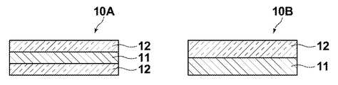
- FIG. 2 shows a schematic cross-sectional view of specific forms 10A and 10B of the substrate 10.
- the substrates 10A and 10B are substrates obtained by anodizing at least one surface side of the base material 11.
- the base material 11 is a composite base material in which an Al base material containing Al as a main component is combined with at least one surface side of an Fe base material containing Fe as a main component (for example, SUS).
- a base material in which an Al film mainly composed of Al is formed on at least one surface side of an Fe material mainly composed of Fe is preferable.
- a substrate 10A shown in the left diagram of FIG. 2 has an anodized film 12 formed on both surfaces of a base material 11, and a substrate 10B shown in the right diagram of FIG. Is formed.
- the anodic oxide film 12 is a film mainly composed of Al 2 O 3 .
- the anodic oxide film 12 is formed on both surfaces.
- Anodization can be performed by a known method in which a substrate 11 that has been subjected to cleaning treatment, polishing smoothing treatment, or the like as necessary is immersed in an electrolyte together with a cathode, and a voltage is applied between the anode and the cathode.
- the thickness of the substrate 11 and the anodic oxide film 12 is not particularly limited. Considering the mechanical strength of the substrate 10 and reduction in thickness and weight, the thickness of the base material 11 before anodization is preferably 0.05 to 0.6 mm, for example, and more preferably 0.1 to 0.3 mm. Considering the insulating properties of the substrate, mechanical strength, and reduction in thickness and weight, the thickness of the anodic oxide film 12 is preferably 0.1 to 100 ⁇ m, for example.
- the substrate 10 may be one in which a soda lime glass (SLG) layer is provided on the anodic oxide film 12.
- SSG soda lime glass
- Na can be diffused in the photoelectric conversion layer.
- the photoelectric conversion layer contains Na, the photoelectric conversion efficiency can be further improved.
- the constituent elements constituting the conductive layer 20 are not particularly limited as long as they are transition metals that can be used as electrodes. In particular, Mo, Cr, W, and combinations thereof are preferable, and Mo is particularly preferable.
- the film thickness of the conductive layer 20 is not limited and is preferably about 200 to 1000 nm.
- the main component of the photoelectric conversion layer 30 is at least one compound semiconductor composed of a group Ib element, a group IIIb element, and a group VIb element. Specifically, at least one Ib group element selected from the group consisting of Cu and Ag, At least one group IIIb element selected from the group consisting of Al, Ga and In; It is preferably at least one compound semiconductor comprising at least one VIb group element selected from the group consisting of S, Se, and Te.
- the film thickness of the photoelectric conversion layer 30 is not particularly limited and is preferably 1.0 to 3.0 ⁇ m, particularly preferably 1.5 to 2.5
- the buffer layer 40 is a layer mainly composed of CdS, ZnS, Zn (S, O), and Zn (S, O, OH).
- the thickness of the buffer layer 40 is not particularly limited, and is preferably 10 nm to 500 nm, and more preferably 15 to 200 nm.
- the window layer 50 is an intermediate layer that captures light.
- the composition of the window layer 50 is not particularly limited, and i-ZnO or the like is preferable.
- the film thickness of the window layer 50 is not particularly limited and is preferably 15 to 200 nm.
- the window layer is an arbitrary layer and may be a photoelectric conversion element without the window layer 50.
- the transparent electrode 60 is a layer that takes in light and functions as an electrode.
- the composition of the transparent electrode 60 is not particularly limited, and n-ZnO such as ZnO: Al is preferable.
- the film thickness of the transparent electrode 60 is not particularly limited, and is preferably 50 nm to 2 ⁇ m.
- the extraction electrode 70 is an electrode for efficiently extracting electric power generated between the back electrode 20 and the transparent electrode 60 to the outside.
- the main component of the extraction electrode 70 is not particularly limited, and examples thereof include Al.
- the film thickness of the extraction electrode 70 is not particularly limited and is preferably 0.1 to 3 ⁇ m.
- the photoelectric conversion element 1 can be preferably used as a solar cell.
- a large number of the photoelectric conversion elements 1 can be integrated, and a cover glass, a protective film, or the like can be attached as necessary to form a solar cell.
- An integrated solar cell includes, for example, a process of forming each layer on a substrate by a roll-to-roll method using a flexible long substrate, and a patterning (scribing) process for integration. It is formed through an element forming process, a process of cutting the element-formed substrate into one module, and the like.
- the photoelectric conversion element of the present invention having high adhesion between the conductive layer and the photoelectric conversion layer is very effective.
- the photoelectric conversion element manufactured by the manufacturing method of the present invention can be applied not only to solar cells but also to other uses such as a CCD.
- the substrate 10 is prepared, and the conductive layer 20 is formed on the substrate 10.
- the conductive layer 20 is formed by a sputtering method.
- Mo is used as the transition metal
- a Mo layer is formed on the substrate 10 by sputtering.
- the sputtering pressure during the Mo layer sputtering is set to a conventional value in order to prevent the c-axis of the microcrystal of the transition metal dichalcogenide thin film from being uniformly oriented in the direction perpendicular to the conductive layer. Increase compared to sputtering pressure.
- the film can be formed so as to give a tensile stress to the film by setting the pressure to 0.5 Pa or more, for example, 1.0 Pa.
- the surface interval in the film thickness direction of the Mo film can be made smaller than that in the bulk (the surface interval in the film thickness direction can be made smaller than in other directions).
- a photoelectric conversion layer 30 made of an Ib, IIIb, or VIb group element is formed on the conductive layer 20 by an evaporation method.
- a CuInGaSe layer is formed.
- the multi-source simultaneous vapor deposition method is particularly suitable.
- Typical methods include a three-step method (JRTuttle et.al, Mat.Res.Soc.Symp.Proc., Vol.426 (1996) p.143., Etc.) and the EC group simultaneous evaporation method ( L. Stolt et al .: Proc. 13th ECPVSEC (1995, Nice) 1451.).
- In the three-stage method first, In, Ga, and Se are co-deposited at a substrate temperature of 400 ° C. in a high vacuum, then heated to 500 to 560 ° C., and Cu and Se are co-deposited. Are further deposited simultaneously to obtain a graded band gap CIGS film with a forbidden band width inclined.
- the EC group method is an improved version of the Bayer method developed by Boeing, which deposits Cu-rich CIGS in the early stage of vapor deposition and In-rich CIGS in the latter half of the process so that it can be applied to the in-line process.
- the Bayer method is described in W.E.Devaney, W.S.Chen, J.M.Stewart, and R.A.Mickelsen: IEEE Trans.Electron.Devices 37 (1990) 428.
- a) a method using ionized Ga (H. Miyazaki, et.al, phys.stat.sol. (a), Vol.203 (2006) p.2603, etc.), b) Method of using cracked Se (The 68th Japan Society of Applied Physics Academic Lecture Proceedings (Autumn 2007, Hokkaido Institute of Technology) 7P-L-6 etc.), c) Method using radicalized Se (The 54th JSAP Scientific Lecture Proceedings (Spring 2007 Aoyama Gakuin University) 29P-ZW-10 etc.), d) A method using a photoexcitation process (the 54th JSAP Scientific Lecture Proceedings (Aoyama Gakuin University, 29P-ZW-14, etc.)) is known.
- Se which is the VIb element of the CIGS layer, reacts with Mo to form the MoSe 2 layer 25.
- the buffer layer 40 is formed on the photoelectric conversion layer 30.
- the buffer layer 40 for example, CdS is formed by a CBD method (chemical bath deposition method) or the like.
- a ZnO layer for example, is formed as the window layer 50 on the surface of the CdS buffer layer 40, and an Al—ZnO layer, for example, is formed as the transparent electrode 60 by sputtering.
- an Al layer is formed on the surface of the transparent electrode 60 by vapor deposition to form the photoelectric conversion element 1.
- each step such as a conductive layer forming step and a photoelectric conversion layer forming step includes a supply roll (unwinding roll) formed by winding a long flexible substrate into a roll shape. It is preferable to use a so-called roll-to-roll method using a winding roll for winding a film-formed substrate into a roll.
- Example 2 The sample of the Example of the photoelectric conversion element of this invention was produced with the following method.
- a 3 cm ⁇ 3 cm ⁇ 1.1 mmt soda lime glass substrate was prepared and subjected to ultrasonic cleaning with acetone, ethanol, and pure water for 5 minutes each.
- the substrate was introduced into a sputtering apparatus, and Mo was sputtered on the substrate by RF sputtering at an RF power of 800 W, an Ar gas pressure of 1.0 Pa, and a substrate temperature of room temperature.
- the film formation time was adjusted so that the film thickness was about 600 nm.
- a CdS buffer layer was formed on the surface of the photoelectric conversion layer (CIGS layer) to a thickness of 50 nm by a CBD method (chemical bath deposition method).
- a ZnO layer was formed as a window layer on the surface of the CdS buffer layer to a thickness of 50 nm by sputtering.
- an Al—ZnO layer having a thickness of 300 nm was formed by sputtering as a transparent electrode.
- an Al layer was formed on the surface of the Al—ZnO layer as an extraction electrode by a vapor deposition method.
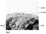
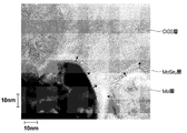
- FIG. 4 show a transmission electron micrograph (TEM image) of a comparative example.
- TEM image transmission electron micrograph
- auxiliary lines are added to make it easy to visually recognize the layer structure (microcrystals).
- the arrow indicates the c-axis direction.
- the ratio of the microcrystals whose c-axis is perpendicular to the surface of the Mo layer to the number of microcrystals formed on the surface of the Mo layer is obtained. It was about 60%.
- the ratio of the microcrystals whose c-axis is perpendicular to the surface of the Mo layer to the number of microcrystals formed on the surface of the Mo layer was determined as follows.
- a sample in which the depth direction (perpendicular to the observation cross-section) is made into a uniform thickness of 100 nm or less by FIB processing, and the sample in which the photoelectric conversion layer-back electrode interface region can be observed is prepared.
- a TEM image of a cross section of the laminated film perpendicular to the substrate surface was taken by transmission electron microscopy. Images used for evaluation were observed at a magnification of 2 million times.
- the field of view was 100 nm ⁇ 100 nm or more.
- the contrast adjustment function of the image processing software PhotoShop (registered trademark)
- the transition metal dichalcogenide thin film is clearly displayed by using the contrast of the photoelectric conversion layer, the transition metal dichalcogenide thin film and the conductive layer in the photographed image.
- the area of the extracted transition metal dichalcogenide fine particle (microcrystal) image is calculated from the number of pixels of the image processing software. The number of pixels was calculated for each fine particle present in the field of view, and the proportion of microcrystals in which the c-axis was formed substantially vertically was calculated.
- the microcrystal in which the c-axis is formed substantially perpendicular refers to a crystal whose c-axis is directed to 90 ° ⁇ 10 ° with respect to the Mo film.
- the MoSe 2 layer which is a transition metal dichalcogenide generated between the conductive layer and the CIGS layer as in the example, contains a large number of microcrystals and the c-axis is perpendicular to the surface of the conductive layer. If the ratio is about 60%, the adhesion should be much better than the sample of the comparative example having a layered MoSe 2 layer over almost the whole area at the interface between the conductive layer and the CIGS layer. Is clear.
Landscapes
- Engineering & Computer Science (AREA)
- Microelectronics & Electronic Packaging (AREA)
- Physics & Mathematics (AREA)
- Condensed Matter Physics & Semiconductors (AREA)
- Electromagnetism (AREA)
- General Physics & Mathematics (AREA)
- Computer Hardware Design (AREA)
- Power Engineering (AREA)
- Chemical & Material Sciences (AREA)
- Crystallography & Structural Chemistry (AREA)
- Sustainable Development (AREA)
- Sustainable Energy (AREA)
- Life Sciences & Earth Sciences (AREA)
- Photovoltaic Devices (AREA)
Abstract
[Problem] To improve adhesion in a photoelectric conversion element provided with a photoelectric conversion layer formed by vapor deposition on an electroconductive layer made of a transition metal. [Solution] A photoelectric conversion element (1) has, on a substrate (10), a multi-layered structure including: an electroconductive layer (20) made of a transition metal element; a photoelectric conversion layer (30) made of a compound semiconductor containing a group IB element, a group IIIB element, and a group VIB element; and a transparent electrode (60), wherein the photoelectric conversion element (1) is configured to comprise, between the electroconductive layer (20) and the photoelectric conversion layer (30), a transition metal dichalcogenide thin film (25) made of a transition metal element and a group VIB element. Of a plurality of microcrystals (25a) constituting the transition metal dichalcogenide thin film (25), microcrystals having a c axis formed substantially perpendicular to the surface of the electroconductive layer (20) occupy no more than 80% of the surface of the electroconductive layer (20) on which the thin film is formed.
Description
本発明は、太陽電池、CCDセンサ等に用いられる光電変換素子に関するものである。
The present invention relates to a photoelectric conversion element used for a solar cell, a CCD sensor or the like.
光電変換層とこれに導通する電極とを備えた光電変換素子が、太陽電池等の用途に使用されている。従来、太陽電池においては、バルクの単結晶Siまたは多結晶Si、あるいは薄膜のアモルファスSiを用いたSi系太陽電池が主流であったが、Siに依存しない化合物半導体系太陽電池の研究開発がなされている。化合物半導体系太陽電池としては、GaAs系等のバルク系と、Ib族元素とIIIb族元素とVIb族元素とからなるCIGS系等の薄膜系とが知られている。CIGSは、一般式Cu1-zIn1-xGaxSe2-ySy(式中、0≦x≦1,0≦y≦2,0≦z≦1)で表される化合物半導体であり、x=0のときがCIS、x>0のときがCIGSである。本明細書では、CIGSはCISを含むものとする。
A photoelectric conversion element including a photoelectric conversion layer and an electrode connected to the photoelectric conversion layer is used for applications such as solar cells. Conventionally, in the case of solar cells, Si-based solar cells using bulk single crystal Si or polycrystalline Si, or thin-film amorphous Si have been mainstream, but research and development of Si-independent compound semiconductor solar cells has been made. ing. As compound semiconductor solar cells, there are known bulk systems such as GaAs systems and thin film systems such as CIGS systems composed of group Ib elements, group IIIb elements and group VIb elements. CIGS has the general formula Cu 1-z In 1-x Ga x Se 2-y S y ( where, 0 ≦ x ≦ 1,0 ≦ y ≦ 2,0 ≦ z ≦ 1) compound represented by the Semiconductor Yes, CIS is when x = 0, and CIGS when x> 0. In this specification, CIGS includes CIS.
CIGS系光電変換素子を製造するにあたっては、積層された層間における剥離の問題が重要である。特に、ロール・トウ・ロール方式による製造を実施する際には、搬送の際に膜にかかる負荷のために、より剥離が生じ易い。剥離の軽減は製造の際の歩留まりを向上させることに貢献するほか、光電変換効率特性の向上にも貢献する。
In manufacturing a CIGS photoelectric conversion element, the problem of delamination between stacked layers is important. In particular, when manufacturing by a roll-to-roll system, peeling is more likely to occur due to the load applied to the film during transport. The reduction of peeling contributes to improving the yield in manufacturing and also contributes to the improvement of photoelectric conversion efficiency characteristics.
CIGS系光電変換素子における剥離の原因は、主に光電変換層であるCIGSと裏面電極であるMo層との界面に形成されるMoSe2層が裏面電極層に対してc軸配向した層状に形成されることにあると言われている(図5参照)。
非特許文献1には、層状に形成されたMoSe2層の層間の結合はファンデルワールス力による弱い結合であるため、層状にMoSe2層が形成されたMo層とCIGS膜との密着性が弱くなると言及されている。
そのため、剥離の軽減を図るために、MoSe2層の形成を抑制する方法が、特許文献1、2、および3等において検討されている。
特許文献1~3においては、CIGS層をセレン化法により形成する場合における、MoSe2層の抑制方法が開示されている。 The cause of peeling in the CIGS photoelectric conversion element is mainly formed in a layered state in which the MoSe 2 layer formed at the interface between the CIGS as the photoelectric conversion layer and the Mo layer as the back electrode is c-axis oriented with respect to the back electrode layer. It is said that it is to be done (see FIG. 5).
InNon-Patent Document 1, since the bond between the layers of the MoSe 2 layer formed in a layered form is a weak bond due to van der Waals force, the adhesion between the Mo layer formed with the MoSe 2 layer in a layered form and the CIGS film is Mentioned to be weak.
Therefore, in order to reduce peeling, methods for suppressing the formation of the MoSe 2 layer are studied inPatent Documents 1, 2, and 3, etc.
Patent Documents 1 to 3 disclose a method of suppressing the MoSe 2 layer when the CIGS layer is formed by a selenization method.
非特許文献1には、層状に形成されたMoSe2層の層間の結合はファンデルワールス力による弱い結合であるため、層状にMoSe2層が形成されたMo層とCIGS膜との密着性が弱くなると言及されている。
そのため、剥離の軽減を図るために、MoSe2層の形成を抑制する方法が、特許文献1、2、および3等において検討されている。
特許文献1~3においては、CIGS層をセレン化法により形成する場合における、MoSe2層の抑制方法が開示されている。 The cause of peeling in the CIGS photoelectric conversion element is mainly formed in a layered state in which the MoSe 2 layer formed at the interface between the CIGS as the photoelectric conversion layer and the Mo layer as the back electrode is c-axis oriented with respect to the back electrode layer. It is said that it is to be done (see FIG. 5).
In
Therefore, in order to reduce peeling, methods for suppressing the formation of the MoSe 2 layer are studied in
一方、Mo層とCIGS層との間にMoSe2層が存在することにより、Mo層とMoSe2層との間にオーミック接触が形成され、太陽電池の効率向上を担っているとの報告がなされている。また、このMoSe2層の代わりに、ZnO等の半導体層をMo層上に形成して変換効率の向上を図ることも提案されている(特許文献4、5等)。
On the other hand, it is reported that the presence of the MoSe 2 layer between the Mo layer and the CIGS layer forms an ohmic contact between the Mo layer and the MoSe 2 layer, and is responsible for improving the efficiency of the solar cell. ing. It has also been proposed to improve the conversion efficiency by forming a semiconductor layer such as ZnO on the Mo layer instead of the MoSe 2 layer (Patent Documents 4, 5, etc.).
しかしながら、遷移金属からなる裏面電極上に、蒸着法によりCIGS層を形成する場合における、MoSe2層の抑制方法は未だ確立されておらず、蒸着法を用いてCIGS層が形成されてなる光電変換素子において剥離を抑制することは重要な課題となっている。
なお、裏面電極をMo以外の遷移金属により構成し、光電変換層として、Ib-IIIb-VIb化合物半導体により構成する場合には、遷移金属二カルコゲニド層が裏面電極と光電変換層との間に生成され、同様の問題が生じる。 However, when a CIGS layer is formed by vapor deposition on a back electrode made of a transition metal, a method for suppressing the MoSe 2 layer has not yet been established, and photoelectric conversion in which a CIGS layer is formed using vapor deposition It is an important problem to suppress peeling in the element.
When the back electrode is made of a transition metal other than Mo and the photoelectric conversion layer is made of an Ib-IIIb-VIb compound semiconductor, a transition metal dichalcogenide layer is formed between the back electrode and the photoelectric conversion layer. A similar problem arises.
本発明は上記事情に鑑みなされたものであり、密着性が高く、剥離が生じにくい光電変換素子を提供することを目的とするものである。
The present invention has been made in view of the above circumstances, and an object of the present invention is to provide a photoelectric conversion element that has high adhesion and is less likely to be peeled off.
基板上に、遷移金属元素からなる導電層と、Ib族元素、IIIb族元素およびVIb族元素を含有する化合物半導体からなる光電変換層と、透明電極との積層構造を有する光電変換素子であって、
前記導電層と前記光電変換層との間に、前記遷移金属元素と前記VIb族元素とからなる遷移金属二カルコゲニド薄膜を備え、
該遷移金属二カルコゲニド薄膜が、微結晶を多数含み、該多数の微結晶のうち、前記導電層の表面にc軸が略垂直に形成されている微結晶の、該薄膜が形成されている導電層の表面に占める割合が80%以下であることを特徴とするものである。 A photoelectric conversion element having a laminated structure of a conductive layer made of a transition metal element, a photoelectric conversion layer made of a compound semiconductor containing a group Ib element, a group IIIb element and a group VIb element on a substrate, and a transparent electrode. ,
A transition metal dichalcogenide thin film comprising the transition metal element and the VIb group element is provided between the conductive layer and the photoelectric conversion layer,
The transition metal dichalcogenide thin film includes a large number of microcrystals, and among the large number of microcrystals, the conductive film on which the thin film is formed is a microcrystal in which the c-axis is formed substantially perpendicularly on the surface of the conductive layer. The proportion of the layer on the surface is 80% or less.
c軸が略垂直に形成されている微結晶の、導電層の表面に占める割合は、以下のようにして算出した値とする。
1)透過電子顕微鏡法(TEM:transmission electron microscopy)により、積層膜の、基板面に対して垂直な断面のTEM像(特に光電変換層―裏面電極界面領域)を撮影する。これを原画像とする。
2)TEM像において光電変換層と遷移金属二カルコゲニド薄膜と導電層のコントラストが異なることを利用し、画像処理ソフトのコントラスト調整機能を利用して、所定のしきい値で2値化し、画像処理ソフトのエッジ抽出機能を用いて抽出する。この場合のしきい値は、できるだけノイズを除去するとともに明らかに遷移金属二カルコゲニド薄膜と判別できるものだけが抽出されるようにする。2値化画像において遷移金属二カルコゲニドと判別できるものだけが抽出されるようにする。2値化画像において遷移金属二カルコゲニド薄膜の輪郭が不鮮明な場合、2値化画像を見ながら経験的に輪郭線を引く。
3)抽出した遷移金属二カルコゲニドの微粒子(微結晶)の像の、面積を画像処理ソフトのピクセル数から算出する。視野に存在するそれぞれの微粒子についてピクセル数を算出し、全体に占める、c軸が略垂直形成されている微結晶の割合を算出する。
1)においてTEM像を撮影するサンプルは、倍率を200万倍で観察するものとする。また視野は100nm×100nm以上とする。
奥行き方向(観察断面と垂直方向)は100nm以下の均一な厚みとなるように加工されたものとする。また、測定において、電子線は、基板面に対して垂直方向に入射させるものとする。画像処理ソフトとしては、例えばPhotoShop(登録商標)を利用するものとする。
なお、本明細書においては、c軸が略垂直形成されている微結晶が導電層の表面に占める割合が80%以下のものは優先配向していない、ランダムな配向であると看做している。 The proportion of the microcrystals with the c-axis formed substantially perpendicular to the surface of the conductive layer is a value calculated as follows.
1) Take a TEM image (particularly the photoelectric conversion layer-back electrode interface region) of the cross section of the laminated film perpendicular to the substrate surface by transmission electron microscopy (TEM). This is the original image.
2) Utilizing the fact that the contrast of the photoelectric conversion layer, transition metal dichalcogenide thin film and conductive layer in the TEM image is different, using the contrast adjustment function of the image processing software, binarization is performed at a predetermined threshold, and image processing is performed. Extract using the soft edge extraction function. The threshold value in this case is to remove noise as much as possible and extract only those that can be clearly distinguished from transition metal dichalcogenide thin films. Only binarized images that can be distinguished from transition metal dichalcogenides are extracted. When the contour of the transition metal dichalcogenide thin film is unclear in the binarized image, the contour line is drawn empirically while viewing the binarized image.
3) The area of the extracted transition metal dichalcogenide fine particle (microcrystal) image is calculated from the number of pixels of the image processing software. The number of pixels is calculated for each fine particle present in the field of view, and the proportion of microcrystals in which the c-axis is formed substantially vertically is calculated.
The sample for taking a TEM image in 1) shall be observed at a magnification of 2 million times. The field of view is 100 nm × 100 nm or more.
It is assumed that the depth direction (perpendicular to the observation cross section) is processed to have a uniform thickness of 100 nm or less. In the measurement, an electron beam is incident in a direction perpendicular to the substrate surface. For example, PhotoShop (registered trademark) is used as the image processing software.
Note that in this specification, the proportion of microcrystals with c-axis formed substantially perpendicular to the surface of the conductive layer is considered to be random orientations that are not preferentially oriented. Yes.
前記導電層が、所定の面を表面に有する配向した多結晶薄膜からなり、膜厚方向の面間隔がバルク結晶の面間隔以下であることが好ましい。
It is preferable that the conductive layer is made of an oriented polycrystalline thin film having a predetermined plane on the surface, and the plane spacing in the film thickness direction is equal to or less than the plane spacing of the bulk crystal.
前記所定の面が(110)であることが特に好ましいが、(100)、(111)面であってもよい。
The predetermined surface is particularly preferably (110), but may be (100) or (111).
前記導電層が、表層の少なくとも一部が、配向していない微結晶を含む薄膜からなるものであってもよい。
The conductive layer may be formed of a thin film containing microcrystals in which at least part of the surface layer is not oriented.
前記導電層が、表層の少なくとも一部が酸化もしくは窒化されていてもよい。
In the conductive layer, at least a part of the surface layer may be oxidized or nitrided.
前記遷移金属元素がMoであることが好ましい。
It is preferable that the transition metal element is Mo.
光電変換層を構成する元素としては、特に、前記Ib族元素が、Cuであり、
前記IIIb族元素が、Al,Ga及びInからなる群より選択された少なくとも1種であり、
前記VIb族元素が、Seであることが好ましい。 As an element constituting the photoelectric conversion layer, in particular, the Ib group element is Cu,
The group IIIb element is at least one selected from the group consisting of Al, Ga and In;
The VIb group element is preferably Se.
前記遷移金属二カルコゲニド薄膜が、MoSe2薄膜であることが好ましい。
The transition metal dichalcogenide thin film is preferably a MoSe 2 thin film.
前記基板が、
Al基材の少なくとも一方の面側にAl2O3陽極酸化膜が形成された陽極酸化基板、
Fe材の少なくとも一方の面側にAl材が複合された複合基材の、少なくとも一方の面側にAl2O3陽極酸化膜が形成された陽極酸化基板、
および、Fe材の少なくとも一方の面側にAl膜が成膜された基材の、少なくとも一方の面側にAl2O3陽極酸化膜が形成された陽極酸化基板、
からなる群より選ばれた陽極酸化基板であることが好ましい。 The substrate is
An anodized substrate in which an Al 2 O 3 anodized film is formed on at least one surface side of an Al base;
An anodized substrate in which an Al 2 O 3 anodized film is formed on at least one surface side of a composite base material in which an Al material is composited on at least one surface side of an Fe material;
And an anodized substrate in which an Al 2 O 3 anodized film is formed on at least one surface side of a base material in which an Al film is formed on at least one surface side of the Fe material,
An anodized substrate selected from the group consisting of
本発明の光電変換素子は、導電層と光電変換層との間に、多数の微結晶を含む遷移金属二カルコゲニド薄膜を備え、その多数の微結晶のうち、導電層の表面にc軸が略垂直に形成されている微結晶の、薄膜が形成されている導電層の表面に占める割合が80%以下とされているので、MoSe2層に代表される遷移金属二カルコゲニド薄膜が一様な層状に裏面電極(導電層)上に形成されている従来の素子と比較して、密着性が高く、剥離抑制効果が高い。
The photoelectric conversion element of the present invention includes a transition metal dichalcogenide thin film containing a large number of microcrystals between a conductive layer and a photoelectric conversion layer, and the c-axis is substantially on the surface of the conductive layer among the large number of microcrystals. Since the proportion of the microcrystals formed vertically in the surface of the conductive layer on which the thin film is formed is 80% or less, the transition metal dichalcogenide thin film represented by the MoSe 2 layer is a uniform layer Compared with the conventional element formed on the back electrode (conductive layer), the adhesiveness is high and the delamination suppressing effect is high.
密着性の向上は歩留まりの向上に繋がり、また、密着性低下に起因する不良部分減少によるモジュールとしての変換効率の向上に繋がる。
Improvement of adhesion leads to improvement of yield, and also leads to improvement of conversion efficiency as a module due to reduction of defective parts caused by adhesion reduction.
以下、図面を参照して、本発明の実施形態にかかる光電変換素子について説明する。
Hereinafter, a photoelectric conversion element according to an embodiment of the present invention will be described with reference to the drawings.
<光電変換素子>
図1Aは本実施形態の光電変換素子1の概略構成を示す断面図、図1Bは、図1Aに示す光電変換素子1の一部を模式的に示した拡大断面図である。視認しやすくするため、図中、各構成要素の縮尺等は実際のものとは適宜異ならせてある。 <Photoelectric conversion element>
1A is a cross-sectional view showing a schematic configuration of thephotoelectric conversion element 1 of the present embodiment, and FIG. 1B is an enlarged cross-sectional view schematically showing a part of the photoelectric conversion element 1 shown in FIG. 1A. In order to facilitate visual recognition, the scale of each component in the figure is appropriately different from the actual one.
図1Aは本実施形態の光電変換素子1の概略構成を示す断面図、図1Bは、図1Aに示す光電変換素子1の一部を模式的に示した拡大断面図である。視認しやすくするため、図中、各構成要素の縮尺等は実際のものとは適宜異ならせてある。 <Photoelectric conversion element>
1A is a cross-sectional view showing a schematic configuration of the
図1Aに示すように、光電変換素子1は、基板10上に、主として遷移金属元素からなり裏面電極として機能する導電層20と光電変換層30とバッファ層40と窓層50と透明電極(透光性導電層)60と取出し電極(グリッド電極)70とが積層された素子であって、導電層20と光電変換層30との間に、遷移金属元素とVIb族元素とからなる遷移金属二カルコゲニド薄膜25を備えている。なお、光電変換層は蒸着法により形成される。
As shown in FIG. 1A, the photoelectric conversion element 1 includes a conductive layer 20, a photoelectric conversion layer 30, a buffer layer 40, a window layer 50, a transparent electrode (transparent electrode) made of a transition metal element and functioning as a back electrode. A photoconductive layer) 60 and a take-out electrode (grid electrode) 70, and a transition metal layer composed of a transition metal element and a VIb group element between the conductive layer 20 and the photoelectric conversion layer 30; A chalcogenide thin film 25 is provided. Note that the photoelectric conversion layer is formed by a vapor deposition method.
なお、図1Bに、導電層20、遷移金属二カルコゲニド薄膜25および光電変換層30を拡大して示すように、遷移金属二カルコゲニド薄膜25は、微結晶25aを多数含む多結晶体であり、多数の微結晶25aのうち、導電層20の表面にc軸が略垂直に形成されている微結晶の、薄膜が形成されている導電層20の表面に占める割合が80%以下であることを特徴とする。図1Bにおいて、微結晶25a中に示されている矢印はc軸方向を示している。
As shown in FIG. 1B in which the conductive layer 20, the transition metal dichalcogenide thin film 25, and the photoelectric conversion layer 30 are enlarged, the transition metal dichalcogenide thin film 25 is a polycrystalline body including a large number of microcrystals 25a. Among the microcrystals 25a, the proportion of the microcrystals whose c-axis is formed substantially perpendicular to the surface of the conductive layer 20 in the surface of the conductive layer 20 on which the thin film is formed is 80% or less. And In FIG. 1B, the arrow shown in the microcrystal 25a indicates the c-axis direction.
図1Bに示す本発明の光電変換素子1は、微結晶25aのc軸が導電層20の表面に略垂直となっているものと、そうでないものとがランダムに配置形成されている。
ここで、「導電層20の表面にc軸が略垂直に形成されている微結晶の、薄膜が形成されている導電層20の表面に占める割合が80%以下である」とは、導電層20表面に形成されている微結晶数のうち、c軸が表面に垂直となっているものの微結晶数が80%以下であることを意味する。微結晶の大きさは均一ではないが、ここでは、各微結晶は全て一様な平均サイズとみなしている。なお、導電層20表面に形成されている微結晶数のうち、c軸が表面に垂直となっているものの微結晶数が60%以下であることがより好ましい。 In thephotoelectric conversion element 1 of the present invention shown in FIG. 1B, the microcrystals 25a whose c-axis is substantially perpendicular to the surface of the conductive layer 20 and those that are not are randomly arranged.
Here, “the proportion of the microcrystals whose c-axis is formed substantially perpendicular to the surface of theconductive layer 20 in the surface of the conductive layer 20 on which the thin film is formed is 80% or less” means that the conductive layer This means that among the number of microcrystals formed on the 20 surface, the number of microcrystals is 80% or less although the c-axis is perpendicular to the surface. Although the size of the microcrystals is not uniform, all the microcrystals are regarded as a uniform average size here. Of the number of microcrystals formed on the surface of the conductive layer 20, the number of microcrystals whose c-axis is perpendicular to the surface is more preferably 60% or less.
ここで、「導電層20の表面にc軸が略垂直に形成されている微結晶の、薄膜が形成されている導電層20の表面に占める割合が80%以下である」とは、導電層20表面に形成されている微結晶数のうち、c軸が表面に垂直となっているものの微結晶数が80%以下であることを意味する。微結晶の大きさは均一ではないが、ここでは、各微結晶は全て一様な平均サイズとみなしている。なお、導電層20表面に形成されている微結晶数のうち、c軸が表面に垂直となっているものの微結晶数が60%以下であることがより好ましい。 In the
Here, “the proportion of the microcrystals whose c-axis is formed substantially perpendicular to the surface of the
図5は、従来の蒸着法により形成された光電変換層を有する従来の光電変換素子における、導電層20、遷移金属二カルコゲニド薄膜25および光電変換層30の構成を模式的に示す断面図である。図5に示すように、従来は遷移金属二カルコゲニド薄膜25中の微結晶25aは、基体となる導電層20の上にc軸が略垂直となるように配向形成されている。微結晶25aのc軸が導電層20の表面に略垂直となるように配向されることにより、導電層20に対して、層状の遷移金属二カルコゲニド薄膜25が形成され、剥離が生じ易いものとなっている。
FIG. 5 is a cross-sectional view schematically showing the configuration of the conductive layer 20, the transition metal dichalcogenide thin film 25, and the photoelectric conversion layer 30 in a conventional photoelectric conversion element having a photoelectric conversion layer formed by a conventional vapor deposition method. . As shown in FIG. 5, conventionally, the microcrystal 25a in the transition metal dichalcogenide thin film 25 is oriented and formed on the conductive layer 20 serving as a base so that the c-axis is substantially vertical. By aligning the c-axis of the microcrystal 25a so as to be substantially perpendicular to the surface of the conductive layer 20, a layered transition metal dichalcogenide thin film 25 is formed on the conductive layer 20, and peeling is likely to occur. It has become.
なお、図5に示すように、多数の微結晶のc軸がほぼ全域に亘って導電層の表面に略垂直となるように配向している場合、非常に密着性が悪く、剥離しやすいが、図1Bに示すように、図5と比較して微結晶の優先配向度が低く、ランダムに配向されていれば、より詳細には、多数の微結晶中の2割程以上の微結晶がそのc軸が表面に略垂直とは異なる方向となるように形成されていれば、全域に亘って層状に形成されている場合と比較して格段に剥離が抑制されると考えられる。
As shown in FIG. 5, when the c-axis of a large number of microcrystals is oriented so as to be substantially perpendicular to the surface of the conductive layer over almost the entire region, the adhesion is very poor and it is easy to peel off. As shown in FIG. 1B, if the preferential orientation degree of the microcrystal is lower than that in FIG. 5 and is oriented randomly, more specifically, about 20% or more of the microcrystals in a large number of microcrystals. If the c-axis is formed so as to be in a direction different from substantially perpendicular to the surface, it is considered that peeling is remarkably suppressed as compared with the case where the c-axis is formed in a layer shape over the entire region.
遷移金属二カルコゲニド薄膜の微結晶のc軸を導電層に垂直な方向に一様配向とさせないための手法としては、以下の方法が挙げられる。
As a method for preventing the c-axis of the microcrystal of the transition metal dichalcogenide thin film from being uniformly oriented in the direction perpendicular to the conductive layer, the following method may be mentioned.
第1の方法は、導電層20を、所定の面を表面に有する配向した多結晶薄膜からなるものとして、膜厚方向の面間隔がバルク結晶の面間隔以下となるようにする方法である。このときの所定の面は、(111)、(100)、(110)などが挙げられる。
The first method is a method in which the conductive layer 20 is made of an oriented polycrystalline thin film having a predetermined plane on the surface, and the plane spacing in the film thickness direction is less than or equal to the plane spacing of the bulk crystal. Examples of the predetermined surface at this time include (111), (100), and (110).
特に、面間隔がバルク結晶の面間隔より小さくなっていること、すなわち導電層の結晶に引張り応力が掛かっていることがより好ましい。
応力は、導電層形成時のスパッタ圧力に依存し、変化させることができる。スパッタ圧力が大きい場合には膜は上に凸になるように応力が掛かり、すなわち膜は引張られている状態であり、格子が引張られることにより膜厚方向の面間隔は狭くなる。面間隔が小さくなれば、VIb族元素が、導電層の結晶格子内に侵入しにくくなり、層状の遷移金属二カルコゲニド層の形成を抑制することができると考えられる。 In particular, it is more preferable that the face spacing is smaller than the face spacing of the bulk crystal, that is, a tensile stress is applied to the crystal of the conductive layer.
The stress depends on the sputtering pressure at the time of forming the conductive layer and can be changed. When the sputtering pressure is high, the film is stressed so as to protrude upward, that is, the film is in a stretched state, and the lattice spacing is pulled to narrow the surface interval in the film thickness direction. If the interplanar spacing is reduced, the group VIb element is less likely to enter the crystal lattice of the conductive layer, and the formation of a layered transition metal dichalcogenide layer can be suppressed.
第2の方法は、導電層20を、その表層の少なくとも一部が配向していない微結晶を含む薄膜からなるものとする方法である。なお、表層は配向していない多数の微結晶からなる場合の他、アモルファスとなっていてもよい。薄膜の表面の配向度を評価するためには、X線回折の平行ビーム薄膜測定法を用いることができる。これにより薄膜の表面近傍の結晶構造を評価することができる。この手法によって薄膜表面の配向度を評価したときに、ロットゲーリング法による特定の面方向に対する配向度が80%以下の場合に配向していないとする。このような導電層上に光電変換層を形成する場合、層状の遷移金属二カルコゲニドの形成が抑制される。
The second method is a method in which the conductive layer 20 is made of a thin film containing microcrystals in which at least a part of the surface layer is not oriented. In addition, the surface layer may be amorphous in addition to a case where it is composed of a large number of fine crystals that are not oriented. In order to evaluate the degree of orientation of the surface of the thin film, an X-ray diffraction parallel beam thin film measurement method can be used. Thereby, the crystal structure near the surface of the thin film can be evaluated. When the orientation degree of the thin film surface is evaluated by this method, it is assumed that the orientation is not achieved when the orientation degree with respect to a specific plane direction by the Lotgering method is 80% or less. When a photoelectric conversion layer is formed on such a conductive layer, formation of a layered transition metal dichalcogenide is suppressed.
なお、一般にはスパッタ法により導電層を形成すると、(110)配向の導電層ができるため、導電層20の配向性を制御するために、導電層の下層に配向制御層を設けることが好ましい。
配向制御層としては、CrやFeからなる層を用いることができ、Cr層がより好ましい。 In general, when a conductive layer is formed by sputtering, a (110) -oriented conductive layer is formed. Therefore, in order to control the orientation of theconductive layer 20, it is preferable to provide an orientation control layer below the conductive layer.
As the orientation control layer, a layer made of Cr or Fe can be used, and a Cr layer is more preferable.
配向制御層としては、CrやFeからなる層を用いることができ、Cr層がより好ましい。 In general, when a conductive layer is formed by sputtering, a (110) -oriented conductive layer is formed. Therefore, in order to control the orientation of the
As the orientation control layer, a layer made of Cr or Fe can be used, and a Cr layer is more preferable.
第3の方法は、導電層20の表層の少なくとも一部を酸化もしくは窒化する方法である。導電層20の形成後、導電層の表面に対して酸素プラズマ処理、あるいは窒素プラズマ処理を施すことに表層を酸化あるいは窒化することができる。遷移金属からなる導電層中に10at.%以下の窒素もしくは酸素を含有させることにより導電層の配向を1軸配向ではなくすることができる(1軸配向とは膜厚方向に面が揃っている状態で、面内方向はランダムな面方位を向いている。ここでは1軸配向は、膜厚方向の配向度が90%以上である場合と定義する。)。なお、遷移金属中に10at.%以上の窒素もしくは酸素が含有されると、遷移金属窒化物もしくは遷移金属酸化物の結晶ができてしまい、遷移金属二カルコゲニドの成長そのものが抑制されてしまう。
The third method is a method of oxidizing or nitriding at least a part of the surface layer of the conductive layer 20. After the formation of the conductive layer 20, the surface layer can be oxidized or nitrided by subjecting the surface of the conductive layer to oxygen plasma treatment or nitrogen plasma treatment. By incorporating nitrogen or oxygen of 10 at.% Or less into the conductive layer made of transition metal, the orientation of the conductive layer can be made not the uniaxial orientation (the uniaxial orientation means that the surfaces are aligned in the film thickness direction. In the state, the in-plane direction faces a random plane orientation, where uniaxial orientation is defined as a case where the orientation degree in the film thickness direction is 90% or more.) If the transition metal contains 10 at.% Or more of nitrogen or oxygen, a transition metal nitride or transition metal oxide crystal is formed and the growth of the transition metal dichalcogenide itself is suppressed.
第4の方法は、光電変換層の成膜条件を調整する方法である。遷移金属二カルコゲニドが形成されるのは光電変換層を成膜するときであるため、光電変換層の蒸着する際の基板温度、蒸着のレート、蒸着源の元素種を調整する。具体的には、初期(蒸着初期)の基板温度を下げる方法があげられる。成膜の初期だけ基板温度を低くすることで、遷移金属とカルコゲンの反応が起こりづらい状態で遷移金属上に光電変換層を形成してやり、その光電変換層によってその後のカルコゲンと遷移金属の反応を抑えることができる。カルコゲンと遷移金属との反応が抑えられた状態(すなわち反応速度が低い状態)とすることにより、遷移金属二カルコゲニドの軸配向を抑制することができる。
The fourth method is a method of adjusting the film forming conditions of the photoelectric conversion layer. Since the transition metal dichalcogenide is formed when the photoelectric conversion layer is formed, the substrate temperature at the time of vapor deposition of the photoelectric conversion layer, the vapor deposition rate, and the element type of the vapor deposition source are adjusted. Specifically, there is a method of lowering the substrate temperature at the initial stage (initial stage of vapor deposition). By lowering the substrate temperature only at the initial stage of film formation, a photoelectric conversion layer is formed on the transition metal in a state where the reaction between the transition metal and the chalcogen hardly occurs, and the subsequent reaction between the chalcogen and the transition metal is suppressed by the photoelectric conversion layer. be able to. By setting the state where the reaction between the chalcogen and the transition metal is suppressed (that is, the state where the reaction rate is low), the axial orientation of the transition metal dichalcogenide can be suppressed.
一般に、基板上にスパッタにより形成される遷移金属からなる導電層においては、遷移金属の柱状結晶が形成され易く、この柱状結晶の表面に対して、層状に遷移金属二カルコゲニド薄膜層が生成される。そのため、第1から第3の方法のように、導電層の表面の状態を変化させることにより、導電層の表面に生成される遷移金属二カルコゲニド薄膜の配向状態を変化させることができると考えられる。
Generally, in a conductive layer made of a transition metal formed by sputtering on a substrate, transition metal columnar crystals are easily formed, and a transition metal dichalcogenide thin film layer is formed in a layered manner on the surface of the columnar crystals. . Therefore, it is considered that the orientation state of the transition metal dichalcogenide thin film generated on the surface of the conductive layer can be changed by changing the state of the surface of the conductive layer as in the first to third methods. .
他方、第4の方法のように、光電変換層の成膜条件を調整することにより、導電層を構成する遷移金属元素とVIb族元素との反応条件を変化させることができるため、遷移金属二カルコゲニド薄膜の配向状態を変化させることができると考えられる。
On the other hand, by adjusting the film forming conditions of the photoelectric conversion layer as in the fourth method, the reaction conditions of the transition metal element and the VIb group element constituting the conductive layer can be changed. It is considered that the orientation state of the chalcogenide thin film can be changed.
既述の通り、遷移金属二カルコゲニド薄膜が層状に裏面電極上に一様に形成されることにより、光電変換素子における密着性が低下するため、遷移金属二カルコゲニド薄膜を構成する微結晶がランダムに配向されていれば、密着性の低下を抑制する効果を得ることができる。
なお、密着性の低下抑制のためには遷移金属二カルコゲニド薄膜の生成を抑制する方法も検討されうるが、既述の通り、MoSe2層がオーミック接触により光電変換効率の向上に寄与することから、遷移金属二カルコゲニド薄膜の生成を抑制してしまうよりも、配向が制御された遷移金属二カルコゲニド薄膜を備えた本発明の素子は、剥離を抑制することができると共に、光電変換効率の向上も可能となり好ましい。 As described above, since the transition metal dichalcogenide thin film is uniformly formed on the back electrode in a layered manner, the adhesion in the photoelectric conversion element is lowered, so that the microcrystals constituting the transition metal dichalcogenide thin film are randomly formed. If it is oriented, it is possible to obtain an effect of suppressing a decrease in adhesion.
A method for suppressing the formation of transition metal dichalcogenide thin film can be considered for suppressing the decrease in adhesion, but as described above, the MoSe 2 layer contributes to the improvement of photoelectric conversion efficiency by ohmic contact. Rather than suppressing the formation of transition metal dichalcogenide thin film, the element of the present invention comprising a transition metal dichalcogenide thin film with controlled orientation can suppress peeling and also improve photoelectric conversion efficiency. It is possible and preferable.
上述の遷移金属二カルコゲニド薄膜25以外の光電変換素子1を構成する各層の詳細について以下に説明する。
Details of each layer constituting the photoelectric conversion element 1 other than the transition metal dichalcogenide thin film 25 described above will be described below.
(基板)
図2は基板10の具体的な形態10Aおよび10Bの概略断面図を示すものである。基板10A,10Bは基材11の少なくとも一方の面側を陽極酸化して得られた基板である。基材11は、Alを主成分とするAl基材、Feを主成分とするFe材(例えば、SUS)の少なくとも一方の面側にAlを主成分とするAl材が複合された複合基材、あるいはFeを主成分とするFe材の少なくとも一方の面側にAlを主成分とするAl膜が成膜された基材であることが好ましい。 (substrate)
FIG. 2 shows a schematic cross-sectional view of specific forms 10A and 10B of the substrate 10. The substrates 10A and 10B are substrates obtained by anodizing at least one surface side of the base material 11. The base material 11 is a composite base material in which an Al base material containing Al as a main component is combined with at least one surface side of an Fe base material containing Fe as a main component (for example, SUS). Alternatively, a base material in which an Al film mainly composed of Al is formed on at least one surface side of an Fe material mainly composed of Fe is preferable.
図2は基板10の具体的な形態10Aおよび10Bの概略断面図を示すものである。基板10A,10Bは基材11の少なくとも一方の面側を陽極酸化して得られた基板である。基材11は、Alを主成分とするAl基材、Feを主成分とするFe材(例えば、SUS)の少なくとも一方の面側にAlを主成分とするAl材が複合された複合基材、あるいはFeを主成分とするFe材の少なくとも一方の面側にAlを主成分とするAl膜が成膜された基材であることが好ましい。 (substrate)
FIG. 2 shows a schematic cross-sectional view of
図2の左図に示す基板10Aは、基材11の両面に陽極酸化膜12が形成されたものであり、図2の右図に示す基板10Bは、基材11の片面に陽極酸化膜12が形成されたものである。陽極酸化膜12はAl2O3を主成分とする膜である。デバイスの製造過程において、AlとAl2O3との熱膨張係数差に起因した基板の反り、およびこれによる膜剥がれ等を抑制するには、図2の左図に示すように基材11の両面に陽極酸化膜12が形成されたものがより好ましい。
A substrate 10A shown in the left diagram of FIG. 2 has an anodized film 12 formed on both surfaces of a base material 11, and a substrate 10B shown in the right diagram of FIG. Is formed. The anodic oxide film 12 is a film mainly composed of Al 2 O 3 . In order to suppress the warpage of the substrate due to the difference in thermal expansion coefficient between Al and Al 2 O 3 and the film peeling due to this in the device manufacturing process, as shown in the left diagram of FIG. More preferably, the anodic oxide film 12 is formed on both surfaces.
陽極酸化は、必要に応じて洗浄処理・研磨平滑化処理等が施された基材11を陽極とし陰極と共に電解質に浸漬させ、陽極陰極間に電圧を印加する周知の方法で行うことができる。
Anodization can be performed by a known method in which a substrate 11 that has been subjected to cleaning treatment, polishing smoothing treatment, or the like as necessary is immersed in an electrolyte together with a cathode, and a voltage is applied between the anode and the cathode.
基材11および陽極酸化膜12の厚みは特に制限されない。基板10の機械的強度および薄型軽量化等を考慮すれば、陽極酸化前の基材11の厚みは例えば0.05~0.6mmが好ましく、0.1~0.3mmがより好ましい。基板の絶縁性、機械的強度、および薄型軽量化を考慮すれば、陽極酸化膜12の厚みは例えば0.1~100μmが好ましい。
The thickness of the substrate 11 and the anodic oxide film 12 is not particularly limited. Considering the mechanical strength of the substrate 10 and reduction in thickness and weight, the thickness of the base material 11 before anodization is preferably 0.05 to 0.6 mm, for example, and more preferably 0.1 to 0.3 mm. Considering the insulating properties of the substrate, mechanical strength, and reduction in thickness and weight, the thickness of the anodic oxide film 12 is preferably 0.1 to 100 μm, for example.
さらに、基板10は、陽極酸化膜12上にソーダライムガラス(SLG)層が設けられたものであってもよい。ソーダライムガラス層を備えることにより、光電変換層にNaを拡散させることができる。光電変換層がNaを含むことにより、光電変換効率をさらに向上させることができる。
Further, the substrate 10 may be one in which a soda lime glass (SLG) layer is provided on the anodic oxide film 12. By providing the soda lime glass layer, Na can be diffused in the photoelectric conversion layer. When the photoelectric conversion layer contains Na, the photoelectric conversion efficiency can be further improved.
(導電層(裏面電極))
導電層20を構成する構成元素は、電極として用いることができる遷移金属であれば特に限定されないが、特には、Mo,Cr,W,およびこれらの組合せが好ましく、Moが特に好ましい。導電層20の膜厚は制限されず、200~1000nm程度が好ましい。 (Conductive layer (back electrode))
The constituent elements constituting theconductive layer 20 are not particularly limited as long as they are transition metals that can be used as electrodes. In particular, Mo, Cr, W, and combinations thereof are preferable, and Mo is particularly preferable. The film thickness of the conductive layer 20 is not limited and is preferably about 200 to 1000 nm.
導電層20を構成する構成元素は、電極として用いることができる遷移金属であれば特に限定されないが、特には、Mo,Cr,W,およびこれらの組合せが好ましく、Moが特に好ましい。導電層20の膜厚は制限されず、200~1000nm程度が好ましい。 (Conductive layer (back electrode))
The constituent elements constituting the
(光電変換層)
光電変換層30の主成分は、Ib族元素とIIIb族元素とVIb族元素とからなる少なくとも1種の化合物半導体である。
具体的には、CuおよびAgからなる群より選択された少なくとも1種のIb族元素と、
Al,GaおよびInからなる群より選択された少なくとも1種のIIIb族元素と、
S,Se,およびTeからなる群から選択された少なくとも1種のVIb族元素とからなる少なくとも1種の化合物半導体であることが好ましい。 (Photoelectric conversion layer)
The main component of thephotoelectric conversion layer 30 is at least one compound semiconductor composed of a group Ib element, a group IIIb element, and a group VIb element.
Specifically, at least one Ib group element selected from the group consisting of Cu and Ag,
At least one group IIIb element selected from the group consisting of Al, Ga and In;
It is preferably at least one compound semiconductor comprising at least one VIb group element selected from the group consisting of S, Se, and Te.
光電変換層30の主成分は、Ib族元素とIIIb族元素とVIb族元素とからなる少なくとも1種の化合物半導体である。
具体的には、CuおよびAgからなる群より選択された少なくとも1種のIb族元素と、
Al,GaおよびInからなる群より選択された少なくとも1種のIIIb族元素と、
S,Se,およびTeからなる群から選択された少なくとも1種のVIb族元素とからなる少なくとも1種の化合物半導体であることが好ましい。 (Photoelectric conversion layer)
The main component of the
Specifically, at least one Ib group element selected from the group consisting of Cu and Ag,
At least one group IIIb element selected from the group consisting of Al, Ga and In;
It is preferably at least one compound semiconductor comprising at least one VIb group element selected from the group consisting of S, Se, and Te.
上記化合物半導体としては、
CuAlS2,CuGaS2,CuInS2,
CuAlSe2,CuGaSe2,
AgAlS2,AgGaS2,AgInS2,
AgAlSe2,AgGaSe2,AgInSe2,
AgAlTe2,AgGaTe2,AgInTe2,
Cu(In,Al)Se2,Cu(In,Ga)(S,Se)2,
Cu1-zIn1-xGaxSe2-ySy(式中、0≦x≦1,0≦y≦2,0≦z≦1)(CI(G)S),
Ag(In,Ga)Se2,およびAg(In,Ga)(S,Se)2等が挙げられる。
特には、CuInGaSe2が好ましい。
光電変換層30の膜厚は特に制限されず、1.0~3.0μmが好ましく、1.5~2.5μmが特に好ましい。 As the compound semiconductor,
CuAlS 2 , CuGaS 2 , CuInS 2 ,
CuAlSe 2 , CuGaSe 2 ,
AgAlS 2 , AgGaS 2 , AgInS 2 ,
AgAlSe 2 , AgGaSe 2 , AgInSe 2 ,
AgAlTe 2 , AgGaTe 2 , AgInTe 2 ,
Cu (In, Al) Se 2 , Cu (In, Ga) (S, Se) 2 ,
Cu 1-z In 1-x Ga x Se 2-y S y (where 0 ≦ x ≦ 1, 0 ≦ y ≦ 2, 0 ≦ z ≦ 1) (CI (G) S),
Examples include Ag (In, Ga) Se 2 and Ag (In, Ga) (S, Se) 2 .
In particular, CuInGaSe 2 is preferable.
The film thickness of thephotoelectric conversion layer 30 is not particularly limited and is preferably 1.0 to 3.0 μm, particularly preferably 1.5 to 2.5 μm.
CuAlS2,CuGaS2,CuInS2,
CuAlSe2,CuGaSe2,
AgAlS2,AgGaS2,AgInS2,
AgAlSe2,AgGaSe2,AgInSe2,
AgAlTe2,AgGaTe2,AgInTe2,
Cu(In,Al)Se2,Cu(In,Ga)(S,Se)2,
Cu1-zIn1-xGaxSe2-ySy(式中、0≦x≦1,0≦y≦2,0≦z≦1)(CI(G)S),
Ag(In,Ga)Se2,およびAg(In,Ga)(S,Se)2等が挙げられる。
特には、CuInGaSe2が好ましい。
光電変換層30の膜厚は特に制限されず、1.0~3.0μmが好ましく、1.5~2.5μmが特に好ましい。 As the compound semiconductor,
CuAlS 2 , CuGaS 2 , CuInS 2 ,
CuAlSe 2 , CuGaSe 2 ,
AgAlS 2 , AgGaS 2 , AgInS 2 ,
AgAlSe 2 , AgGaSe 2 , AgInSe 2 ,
AgAlTe 2 , AgGaTe 2 , AgInTe 2 ,
Cu (In, Al) Se 2 , Cu (In, Ga) (S, Se) 2 ,
Cu 1-z In 1-x Ga x Se 2-y S y (where 0 ≦ x ≦ 1, 0 ≦ y ≦ 2, 0 ≦ z ≦ 1) (CI (G) S),
Examples include Ag (In, Ga) Se 2 and Ag (In, Ga) (S, Se) 2 .
In particular, CuInGaSe 2 is preferable.
The film thickness of the
(バッファ層)
バッファ層40は、CdS、ZnS、Zn(S,O)、Zn(S,O,OH)、を主成分とする層からなる。バッファ層40の膜厚は特に制限されず、10nm~500nmが好ましく、15~200nmがより好ましい。 (Buffer layer)
Thebuffer layer 40 is a layer mainly composed of CdS, ZnS, Zn (S, O), and Zn (S, O, OH). The thickness of the buffer layer 40 is not particularly limited, and is preferably 10 nm to 500 nm, and more preferably 15 to 200 nm.
バッファ層40は、CdS、ZnS、Zn(S,O)、Zn(S,O,OH)、を主成分とする層からなる。バッファ層40の膜厚は特に制限されず、10nm~500nmが好ましく、15~200nmがより好ましい。 (Buffer layer)
The
(窓層)
窓層50は、光を取り込む中間層である。窓層50の組成としては特に制限されず、i-ZnO等が好ましい。窓層50の膜厚は特に制限されず、15~200nmが好ましい。なお、窓層は任意の層であり、窓層50のない光電変換素子としてもよい。 (Window layer)
Thewindow layer 50 is an intermediate layer that captures light. The composition of the window layer 50 is not particularly limited, and i-ZnO or the like is preferable. The film thickness of the window layer 50 is not particularly limited and is preferably 15 to 200 nm. The window layer is an arbitrary layer and may be a photoelectric conversion element without the window layer 50.
窓層50は、光を取り込む中間層である。窓層50の組成としては特に制限されず、i-ZnO等が好ましい。窓層50の膜厚は特に制限されず、15~200nmが好ましい。なお、窓層は任意の層であり、窓層50のない光電変換素子としてもよい。 (Window layer)
The
(透明電極)
透明電極60は、光を取り込むと共に電極として機能する層である。透明電極60の組成としては特に制限されず、ZnO:Al等のn-ZnO等が好ましい。透明電極60の膜厚は特に制限されず、50nm~2μmが好ましい。 (Transparent electrode)
Thetransparent electrode 60 is a layer that takes in light and functions as an electrode. The composition of the transparent electrode 60 is not particularly limited, and n-ZnO such as ZnO: Al is preferable. The film thickness of the transparent electrode 60 is not particularly limited, and is preferably 50 nm to 2 μm.
透明電極60は、光を取り込むと共に電極として機能する層である。透明電極60の組成としては特に制限されず、ZnO:Al等のn-ZnO等が好ましい。透明電極60の膜厚は特に制限されず、50nm~2μmが好ましい。 (Transparent electrode)
The
(取出し電極)
取出し電極70は、裏面電極20および透明電極60間に生じる電力を効率的に外部に取り出すための電極である。
取出し電極70の主成分としては特に制限されず、Al等が挙げられる。取出し電極70膜厚は特に制限されず、0.1~3μmが好ましい。 (Extraction electrode)
Theextraction electrode 70 is an electrode for efficiently extracting electric power generated between the back electrode 20 and the transparent electrode 60 to the outside.
The main component of theextraction electrode 70 is not particularly limited, and examples thereof include Al. The film thickness of the extraction electrode 70 is not particularly limited and is preferably 0.1 to 3 μm.
取出し電極70は、裏面電極20および透明電極60間に生じる電力を効率的に外部に取り出すための電極である。
取出し電極70の主成分としては特に制限されず、Al等が挙げられる。取出し電極70膜厚は特に制限されず、0.1~3μmが好ましい。 (Extraction electrode)
The
The main component of the
光電変換素子1は、太陽電池として好ましく使用することができる。
例えば、上記の光電変換素子1を多数集積化し、必要に応じて、カバーガラス、保護フィルム等を取り付けて、太陽電池とすることができる。なお、多数の光電変換素子(セル)が集積化された太陽電池においては、セル毎に取出し電極を設ける必要はない。集積化太陽電池は、例えば、可撓性の長尺基板を用いてロール・トゥ・ロール方式にて、基板上に各層を形成する工程、集積化のためのパターニング(スクライブ)プロセスを含む光電変換素子形成工程、および素子形成された基板を1モジュールに切断する工程等を経て形成される。なお、ロール・トゥ・ロール方式による製造を行う場合には、スクライブ処理や、各処理工程での基板の巻き取り工程を伴うため、導電層と光電変換層との間の剥離の問題がより顕著となるので、導電層と光電変換層との高い密着性を有する本発明の光電変換素子が非常に有効である。 Thephotoelectric conversion element 1 can be preferably used as a solar cell.
For example, a large number of thephotoelectric conversion elements 1 can be integrated, and a cover glass, a protective film, or the like can be attached as necessary to form a solar cell. Note that in a solar battery in which a large number of photoelectric conversion elements (cells) are integrated, it is not necessary to provide an extraction electrode for each cell. An integrated solar cell includes, for example, a process of forming each layer on a substrate by a roll-to-roll method using a flexible long substrate, and a patterning (scribing) process for integration. It is formed through an element forming process, a process of cutting the element-formed substrate into one module, and the like. In addition, when manufacturing by the roll-to-roll method, since the scribing process and the winding process of the substrate in each processing process are involved, the problem of peeling between the conductive layer and the photoelectric conversion layer is more remarkable. Therefore, the photoelectric conversion element of the present invention having high adhesion between the conductive layer and the photoelectric conversion layer is very effective.
例えば、上記の光電変換素子1を多数集積化し、必要に応じて、カバーガラス、保護フィルム等を取り付けて、太陽電池とすることができる。なお、多数の光電変換素子(セル)が集積化された太陽電池においては、セル毎に取出し電極を設ける必要はない。集積化太陽電池は、例えば、可撓性の長尺基板を用いてロール・トゥ・ロール方式にて、基板上に各層を形成する工程、集積化のためのパターニング(スクライブ)プロセスを含む光電変換素子形成工程、および素子形成された基板を1モジュールに切断する工程等を経て形成される。なお、ロール・トゥ・ロール方式による製造を行う場合には、スクライブ処理や、各処理工程での基板の巻き取り工程を伴うため、導電層と光電変換層との間の剥離の問題がより顕著となるので、導電層と光電変換層との高い密着性を有する本発明の光電変換素子が非常に有効である。 The
For example, a large number of the
なお、本発明の製造方法で作製される光電変換素子は、太陽電池のみならずCCD等の他の用途にも適用可能である。
Note that the photoelectric conversion element manufactured by the manufacturing method of the present invention can be applied not only to solar cells but also to other uses such as a CCD.
<光電変換素子の製造方法>
上述の光電変換素子の製造方法を簡単に説明する。 <Method for producing photoelectric conversion element>
A method for manufacturing the above-described photoelectric conversion element will be briefly described.
上述の光電変換素子の製造方法を簡単に説明する。 <Method for producing photoelectric conversion element>
A method for manufacturing the above-described photoelectric conversion element will be briefly described.
まず、基板10を用意し、基板10上に導電層20を形成する。
導電層20は、スパッタ法により形成する。例えば、遷移金属としてMoを用い、スパッタ法により、Mo層(遷移金属層)を基板10上に形成する。このとき、その後の光電変換層30の形成時に、遷移金属二カルコゲニド薄膜の微結晶のc軸を導電層に垂直な方向に一様配向とさせないために、Mo層スパッタ時のスパッタ圧力を従来のスパッタ圧力と比較して高くする。従来のスパッタ圧力は0.3Pa程度とされているが、0.5Pa以上、例えば1.0Paとすることで膜に対し引張りの応力を与えるように成膜することができる。これによりMo膜の膜厚方向の面間隔をバルクに比べ小さくすることができる(膜厚方向の面間隔を他の方向よりも小さくすることができる)。 First, thesubstrate 10 is prepared, and the conductive layer 20 is formed on the substrate 10.
Theconductive layer 20 is formed by a sputtering method. For example, Mo is used as the transition metal, and a Mo layer (transition metal layer) is formed on the substrate 10 by sputtering. At this time, when the photoelectric conversion layer 30 is subsequently formed, the sputtering pressure during the Mo layer sputtering is set to a conventional value in order to prevent the c-axis of the microcrystal of the transition metal dichalcogenide thin film from being uniformly oriented in the direction perpendicular to the conductive layer. Increase compared to sputtering pressure. Although the conventional sputtering pressure is about 0.3 Pa, the film can be formed so as to give a tensile stress to the film by setting the pressure to 0.5 Pa or more, for example, 1.0 Pa. Thereby, the surface interval in the film thickness direction of the Mo film can be made smaller than that in the bulk (the surface interval in the film thickness direction can be made smaller than in other directions).
導電層20は、スパッタ法により形成する。例えば、遷移金属としてMoを用い、スパッタ法により、Mo層(遷移金属層)を基板10上に形成する。このとき、その後の光電変換層30の形成時に、遷移金属二カルコゲニド薄膜の微結晶のc軸を導電層に垂直な方向に一様配向とさせないために、Mo層スパッタ時のスパッタ圧力を従来のスパッタ圧力と比較して高くする。従来のスパッタ圧力は0.3Pa程度とされているが、0.5Pa以上、例えば1.0Paとすることで膜に対し引張りの応力を与えるように成膜することができる。これによりMo膜の膜厚方向の面間隔をバルクに比べ小さくすることができる(膜厚方向の面間隔を他の方向よりも小さくすることができる)。 First, the
The
その後、導電層20の上に、Ib、IIIb、VIb族元素からなる光電変換層30を蒸着法により形成する。ここでは、CuInGaSe層を形成するものとする。
Thereafter, a photoelectric conversion layer 30 made of an Ib, IIIb, or VIb group element is formed on the conductive layer 20 by an evaporation method. Here, a CuInGaSe layer is formed.
蒸着法のうち、特に多源同時蒸着法を好適である。その代表的な方法としては、3段階法(J.R.Tuttle et.al, Mat.Res.Soc.Symp.Proc.,Vol.426(1996)p.143.等)と、ECグループの同時蒸着法(L.Stolt et al.:Proc.13th ECPVSEC(1995,Nice)1451.等)とが知られている。
Of the vapor deposition methods, the multi-source simultaneous vapor deposition method is particularly suitable. Typical methods include a three-step method (JRTuttle et.al, Mat.Res.Soc.Symp.Proc., Vol.426 (1996) p.143., Etc.) and the EC group simultaneous evaporation method ( L. Stolt et al .: Proc. 13th ECPVSEC (1995, Nice) 1451.).
3段階法は、高真空中で最初にIn、Ga、Seを基板温度400℃で同時蒸着し、次に500~560℃に昇温してCu、Seを同時蒸着後、In、Ga、Seを更に同時蒸着する方法で、禁制帯幅が傾斜したグレーデッドバンドギャップCIGS膜が得られる。ECグループの方法は、蒸着初期にCu過剰CIGS、後半でIn過剰CIGSを蒸着するBoeing社の開発したバイレーヤー法をインラインプロセスに適用できるように改良したものである。バイレーヤー法は、W.E.Devaney,W.S.Chen,J.M.Stewart,and R.A.Mickelsen:IEEE Trans.Electron.Devices 37(1990)428.に記載されている。
In the three-stage method, first, In, Ga, and Se are co-deposited at a substrate temperature of 400 ° C. in a high vacuum, then heated to 500 to 560 ° C., and Cu and Se are co-deposited. Are further deposited simultaneously to obtain a graded band gap CIGS film with a forbidden band width inclined. The EC group method is an improved version of the Bayer method developed by Boeing, which deposits Cu-rich CIGS in the early stage of vapor deposition and In-rich CIGS in the latter half of the process so that it can be applied to the in-line process. The Bayer method is described in W.E.Devaney, W.S.Chen, J.M.Stewart, and R.A.Mickelsen: IEEE Trans.Electron.Devices 37 (1990) 428.
3段階法及びECグループの同時蒸着法は共に、膜成長過程でCu過剰なCIGS膜組成とし、相分離した液相Cu2-xSe(x=0~1)による液相焼結を利用するため、大粒径化が起こり、結晶性に優れたCIGS膜が形成されるという利点がある。更に、近年CIGS膜の結晶性を向上させるため、この方法に加えた種々の方法に関する検討が行われており、これらを用いてもよい。
Both the three-stage method and the EC group co-evaporation method use a CI-excess CIGS film composition in the film growth process and use liquid phase sintering with phase separated liquid phase Cu 2-x Se (x = 0 to 1). Therefore, there is an advantage that the CIGS film having a large particle size and excellent crystallinity is formed. Furthermore, in recent years, in order to improve the crystallinity of the CIGS film, various methods in addition to this method have been studied, and these may be used.
CIGS膜の結晶性を向上させるため、上記方法に改良を加えた方法として、
a)イオン化したGaを使用する方法(H.Miyazaki, et.al, phys.stat.sol.(a),Vol.203(2006)p.2603.等)、
b)クラッキングしたSeを使用する方法(第68回応用物理学会学術講演会 講演予稿集(2007秋 北海道工業大学)7P-L-6等)、
c)ラジカル化したSeを用いる方法(第54回応用物理学会学術講演会 講演予稿集(2007春 青山学院大学)29P-ZW-10等)、
d)光励起プロセスを利用した方法(第54回応用物理学会学術講演会 講演予稿集(2007春 青山学院大学)29P-ZW-14等)等が知られている。 In order to improve the crystallinity of the CIGS film, as a method of improving the above method,
a) a method using ionized Ga (H. Miyazaki, et.al, phys.stat.sol. (a), Vol.203 (2006) p.2603, etc.),
b) Method of using cracked Se (The 68th Japan Society of Applied Physics Academic Lecture Proceedings (Autumn 2007, Hokkaido Institute of Technology) 7P-L-6 etc.),
c) Method using radicalized Se (The 54th JSAP Scientific Lecture Proceedings (Spring 2007 Aoyama Gakuin University) 29P-ZW-10 etc.),
d) A method using a photoexcitation process (the 54th JSAP Scientific Lecture Proceedings (Aoyama Gakuin University, 29P-ZW-14, etc.)) is known.
この光電変換層の形成の際に、CIGS層のVIb元素であるSeがMoと反応してMoSe2層25が形成される。
During the formation of the photoelectric conversion layer, Se, which is the VIb element of the CIGS layer, reacts with Mo to form the MoSe 2 layer 25.
光電変換層30の形成後、光電変換層30の上にバッファ層40を形成する。バッファ層40としては、例えばCdSを、CBD法(化学浴析出法)等により形成する。
After forming the photoelectric conversion layer 30, the buffer layer 40 is formed on the photoelectric conversion layer 30. As the buffer layer 40, for example, CdS is formed by a CBD method (chemical bath deposition method) or the like.
次いで、CdSバッファ層40の表面に窓層50として、たとえばZnO層を、さらに、透明電極60として、例えばAl-ZnO層をスパッタ法により形成する。
最後に、透明電極60の表面に、取出し電極70として、例えばAl層を蒸着法により形成して光電変換素子1とする。 Next, a ZnO layer, for example, is formed as thewindow layer 50 on the surface of the CdS buffer layer 40, and an Al—ZnO layer, for example, is formed as the transparent electrode 60 by sputtering.
Finally, as theextraction electrode 70, for example, an Al layer is formed on the surface of the transparent electrode 60 by vapor deposition to form the photoelectric conversion element 1.
最後に、透明電極60の表面に、取出し電極70として、例えばAl層を蒸着法により形成して光電変換素子1とする。 Next, a ZnO layer, for example, is formed as the
Finally, as the
基板として可撓性を有する基板を用いる場合、導電層形成工程、光電変換層形成などの各工程は、長尺な可撓性基板をロール状に巻回してなる供給ロール(巻出しロール)と、成膜済の基板をロール状に巻回する巻取りロールとを用いる、いわゆるロール・トゥ・ロール(Roll to Roll)方式を用いることが好ましい。
When a flexible substrate is used as the substrate, each step such as a conductive layer forming step and a photoelectric conversion layer forming step includes a supply roll (unwinding roll) formed by winding a long flexible substrate into a roll shape. It is preferable to use a so-called roll-to-roll method using a winding roll for winding a film-formed substrate into a roll.
光電変換素子について実施例、比較例のサンプルを作製し、その界面を観察すると共に、密着性試験(クロスカット試験)を行った。
Samples of Examples and Comparative Examples were prepared for the photoelectric conversion elements, and the interfaces were observed and an adhesion test (cross cut test) was performed.
(実施例)
本発明の光電変換素子の実施例のサンプルを、以下の方法で作製した。 (Example)
The sample of the Example of the photoelectric conversion element of this invention was produced with the following method.
本発明の光電変換素子の実施例のサンプルを、以下の方法で作製した。 (Example)
The sample of the Example of the photoelectric conversion element of this invention was produced with the following method.
まず、3cm×3cm×1.1mmtのソーダライムガラス基板を用意し、アセトン,エタノール,純水にて各5分間超音波洗浄を施した。
First, a 3 cm × 3 cm × 1.1 mmt soda lime glass substrate was prepared and subjected to ultrasonic cleaning with acetone, ethanol, and pure water for 5 minutes each.
その後スパッタ装置に基板を導入し、RFスパッタにて、RF電力800W、Arガス圧1.0Pa、基板温度室温にて、基板上にMoをスパッタ成膜した。膜厚が約600nmになるように成膜時間を調整した。
Thereafter, the substrate was introduced into a sputtering apparatus, and Mo was sputtered on the substrate by RF sputtering at an RF power of 800 W, an Ar gas pressure of 1.0 Pa, and a substrate temperature of room temperature. The film formation time was adjusted so that the film thickness was about 600 nm.
次に、光電変換層(半導体層)として、裏面電極上に、いわゆる3段階法によりCu(In0.7Ga0.3)Se2を2μm成膜した。3段階法における2、3段階目の基板温度を550℃とした。なお、Kセル(knudsen-Cell:クヌーセンセル)を蒸発源として用いた。
Next, 2 μm of Cu (In 0.7 Ga 0.3 ) Se 2 was formed as a photoelectric conversion layer (semiconductor layer) on the back electrode by a so-called three-stage method. The substrate temperature in the second and third stages in the three-stage method was set to 550 ° C. In addition, K cell (knudsen-Cell: Knudsen cell) was used as an evaporation source.
次に、光電変換層(CIGS層)の表面にCdSバッファ層を、50nmの厚さにCBD法(化学浴析出法)により成膜した。
次いで、CdSバッファ層の表面に窓層としてZnO層を、50nmの厚さにスパッタ法により形成した。
さらに、透明電極としてAl-ZnO層を、300nmの厚さにスパッタ法により形成した。
最後に、Al-ZnO層の表面に、取出し電極として、Al層を蒸着法により形成した。 Next, a CdS buffer layer was formed on the surface of the photoelectric conversion layer (CIGS layer) to a thickness of 50 nm by a CBD method (chemical bath deposition method).
Next, a ZnO layer was formed as a window layer on the surface of the CdS buffer layer to a thickness of 50 nm by sputtering.
Further, an Al—ZnO layer having a thickness of 300 nm was formed by sputtering as a transparent electrode.
Finally, an Al layer was formed on the surface of the Al—ZnO layer as an extraction electrode by a vapor deposition method.
(比較例)
実施例の製造工程において、基板上にMoをスパッタ成膜する際のArガス圧を0.3Paとした。この点以外は実施例と同様とした。 (Comparative example)
In the manufacturing process of the example, the Ar gas pressure when sputtering Mo on the substrate was 0.3 Pa. Except this point, it was the same as the example.
実施例の製造工程において、基板上にMoをスパッタ成膜する際のArガス圧を0.3Paとした。この点以外は実施例と同様とした。 (Comparative example)
In the manufacturing process of the example, the Ar gas pressure when sputtering Mo on the substrate was 0.3 Pa. Except this point, it was the same as the example.
(界面観察)
実施例と比較例の各方法で作製したサンプルについて、断面を切り出し透過型電子顕微鏡にて導電層とCIGS層との界面を観察した。図3実施例、図4に比較例の透過型電子顕微鏡写真(TEM像)を示す。図3中には層構成(微結晶)について視認しやすくするため、補助線を加えている。また、図3、4中において、矢印はc軸方向を示している。 (Interface observation)
About the sample produced by each method of an Example and a comparative example, the cross section was cut out and the interface of a conductive layer and a CIGS layer was observed with the transmission electron microscope. 3 and FIG. 4 show a transmission electron micrograph (TEM image) of a comparative example. In FIG. 3, auxiliary lines are added to make it easy to visually recognize the layer structure (microcrystals). 3 and 4, the arrow indicates the c-axis direction.
図3、図4に示すように、いずれのサンプルにおいても、Mo層とCIGS層との界面にMoSe2層が形成されていることが確認された。
また、図3に示す実施例のサンプルでは、Mo層上に形成されている多数の微結晶のc軸は様々な方向に向いているのに対し、図4に示す比較例のサンプルにおいては、柱状に形成されたMo層上にMo層の表面に沿ってc軸が表面に垂直となるように配向しており、Mo層の表面に一様に層状のMoSe2層が形成されている様子が観察された。 As shown in FIGS. 3 and 4, it was confirmed that a MoSe 2 layer was formed at the interface between the Mo layer and the CIGS layer in any of the samples.
Further, in the sample of the example shown in FIG. 3, the c-axis of many microcrystals formed on the Mo layer is directed in various directions, whereas in the sample of the comparative example shown in FIG. On the Mo layer formed in a columnar shape, the c-axis is oriented along the surface of the Mo layer so as to be perpendicular to the surface, and a uniform layered MoSe 2 layer is formed on the surface of the Mo layer Was observed.
なお、図3に示す実施例のサンプルについて、微結晶のうち、c軸がMo層表面に垂直となっている微結晶の、Mo層表面に形成されている多数の微結晶数に対する割合を求めたところ約60%であった。
For the sample of the example shown in FIG. 3, the ratio of the microcrystals whose c-axis is perpendicular to the surface of the Mo layer to the number of microcrystals formed on the surface of the Mo layer is obtained. It was about 60%.
c軸がMo層表面に垂直となっている微結晶の、Mo層表面に形成されている多数の微結晶数に対する割合は、以下のようにして求めた。
実施例の方法で作製したサンプルについて、まずFIB加工により奥行き方向(観察断面と垂直方向)は100nm以下の均一な厚みとなるように薄片化し、光電変換層―裏面電極界面領域が観察できる試料を作製した。次にこれを透過電子顕微鏡法により、積層膜の、基板面に対して垂直な断面のTEM像を撮影した。評価に使用する画像は倍率を200万倍で観察するものとした。また視野は100nm×100nm以上とした。
撮影した画像において光電変換層と遷移金属二カルコゲニド薄膜と導電層のコントラストが異なることを利用し、画像処理ソフト(PhotoShop(登録商標))のコントラスト調整機能を利用して明らかに遷移金属二カルコゲニド薄膜と判別できるものだけを抽出した。
抽出した遷移金属二カルコゲニドの微粒子(微結晶)の像の、面積を画像処理ソフトのピクセル数から算出する。視野に存在するそれぞれの微粒子についてピクセル数を算出し、全体に占める、c軸が略垂直形成されている微結晶の割合を算出した。このときc軸が略垂直形成されている微結晶とは、c軸がMo膜に対し90°±10°に向いているものを指すこととした。 The ratio of the microcrystals whose c-axis is perpendicular to the surface of the Mo layer to the number of microcrystals formed on the surface of the Mo layer was determined as follows.
For the sample prepared by the method of the example, first, a sample in which the depth direction (perpendicular to the observation cross-section) is made into a uniform thickness of 100 nm or less by FIB processing, and the sample in which the photoelectric conversion layer-back electrode interface region can be observed is prepared. Produced. Next, a TEM image of a cross section of the laminated film perpendicular to the substrate surface was taken by transmission electron microscopy. Images used for evaluation were observed at a magnification of 2 million times. The field of view was 100 nm × 100 nm or more.
Using the contrast adjustment function of the image processing software (PhotoShop (registered trademark)), the transition metal dichalcogenide thin film is clearly displayed by using the contrast of the photoelectric conversion layer, the transition metal dichalcogenide thin film and the conductive layer in the photographed image. We extracted only those that can be distinguished.
The area of the extracted transition metal dichalcogenide fine particle (microcrystal) image is calculated from the number of pixels of the image processing software. The number of pixels was calculated for each fine particle present in the field of view, and the proportion of microcrystals in which the c-axis was formed substantially vertically was calculated. At this time, the microcrystal in which the c-axis is formed substantially perpendicular refers to a crystal whose c-axis is directed to 90 ° ± 10 ° with respect to the Mo film.
(クロスカット試験)
また、実施例と比較例の各方法で作製したサンプルについて、JIS規格(JIS-K5600)に基づきクロスカット試験を行った。カット間隔を1mmとし、付着力(密着力)試験後の25個の碁盤目およびカット交差部の剥がれ状況により密着性を判断した。剥がれたマスの個数をパーセントで評価し、剥離無し(100%)から全面剥離(0%)としてランク付けをした。
この試験の結果、実施例は100%、比較例は0%であった。 (Cross cut test)
Further, a cross-cut test was performed on samples prepared by the methods of Examples and Comparative Examples based on JIS standards (JIS-K5600). The cut interval was set to 1 mm, and the adhesion was judged based on the 25 grids after the adhesion (adhesion) test and the peeled state of the cut intersections. The number of peeled masses was evaluated as a percentage and ranked from no peel (100%) to full peel (0%).
As a result of this test, the example was 100% and the comparative example was 0%.
以上の結果から、実施例のように、導電層とCIGS層との間に生成された遷移金属二カルコゲニドであるMoSe2層が、多数の微結晶を含みそのc軸が導電層表面に垂直となっている割合が60%程度であれば、導電層とCIGS層との界面にほぼ全域に亘って層状のMoSe2層を備えた比較例のサンプルと比較して、格段に密着性がよいことが明らかである。
From the above results, the MoSe 2 layer, which is a transition metal dichalcogenide generated between the conductive layer and the CIGS layer as in the example, contains a large number of microcrystals and the c-axis is perpendicular to the surface of the conductive layer. If the ratio is about 60%, the adhesion should be much better than the sample of the comparative example having a layered MoSe 2 layer over almost the whole area at the interface between the conductive layer and the CIGS layer. Is clear.
Claims (9)
- 基板上に、遷移金属元素からなる導電層と、Ib族元素、IIIb族元素およびVIb族元素を含有する化合物半導体からなる光電変換層と、透明電極との積層構造を有する光電変換素子であって、
前記導電層と前記光電変換層との間に、前記遷移金属元素と前記VIb族元素とからなる遷移金属二カルコゲニド薄膜を備え、
該遷移金属二カルコゲニド薄膜が、微結晶を多数含み、該多数の微結晶のうち、前記導電層の表面にc軸が略垂直に形成されている微結晶の、該薄膜が形成されている導電層の表面に占める割合が80%以下であることを特徴とする光電変換素子。 A photoelectric conversion element having a laminated structure of a conductive layer made of a transition metal element, a photoelectric conversion layer made of a compound semiconductor containing a group Ib element, a group IIIb element and a group VIb element on a substrate, and a transparent electrode. ,
A transition metal dichalcogenide thin film comprising the transition metal element and the VIb group element is provided between the conductive layer and the photoelectric conversion layer,
The transition metal dichalcogenide thin film includes a large number of microcrystals, and among the large number of microcrystals, the conductive film on which the thin film is formed is a microcrystal in which the c-axis is formed substantially perpendicularly on the surface of the conductive layer. The photoelectric conversion element characterized by the ratio which occupies for the surface of a layer being 80% or less. - 前記導電層が、所定の面を表面に有する配向した多結晶薄膜からなり、膜厚方向の面間隔がバルク結晶の面間隔以下であることを特徴とする請求項1記載の光電変換素子。 2. The photoelectric conversion element according to claim 1, wherein the conductive layer is made of an oriented polycrystalline thin film having a predetermined plane on the surface, and the plane spacing in the film thickness direction is equal to or less than the plane spacing of the bulk crystal.
- 前記所定の面が(110)であることを特徴とする請求項2記載の光電変換素子。 3. The photoelectric conversion element according to claim 2, wherein the predetermined surface is (110).
- 前記導電層が、表層の少なくとも一部が配向していない微結晶を含む薄膜からなることを特徴とする請求項1記載の光電変換素子。 The photoelectric conversion element according to claim 1, wherein the conductive layer is formed of a thin film containing microcrystals in which at least a part of the surface layer is not oriented.
- 前記導電層が、表層の少なくとも一部が酸化もしくは窒化されていることを特徴とする請求項1記載の光電変換素子。 The photoelectric conversion element according to claim 1, wherein at least a part of a surface layer of the conductive layer is oxidized or nitrided.
- 前記遷移金属元素がMoであることを特徴とする請求項1から5いずれか1項記載の光電変換素子。 The photoelectric conversion element according to any one of claims 1 to 5, wherein the transition metal element is Mo.
- 前記Ib族元素が、Cuであり、
前記IIIb族元素が、Al,Ga及びInからなる群より選択された少なくとも1種であり、
前記VIb族元素が、Seであることを特徴とする請求項1から6いずれか1項記載の光電変換素子。 The Ib group element is Cu;
The group IIIb element is at least one selected from the group consisting of Al, Ga and In;
The photoelectric conversion element according to claim 1, wherein the VIb group element is Se. - 前記遷移金属二カルコゲニド薄膜が、MoSe2薄膜であることを特徴とする請求項1から7いずれか1項記載の光電変換素子。 The photoelectric conversion element according to claim 1, wherein the transition metal dichalcogenide thin film is a MoSe 2 thin film.
- 前記基板が、
Al基材の少なくとも一方の面側にAl2O3陽極酸化膜が形成された陽極酸化基板、
Fe材の少なくとも一方の面側にAl材が複合された複合基材の、少なくとも一方の面側にAl2O3陽極酸化膜が形成された陽極酸化基板、
および、Fe材の少なくとも一方の面側にAl膜が成膜された基材の、少なくとも一方の面側にAl2O3陽極酸化膜が形成された陽極酸化基板、
からなる群より選ばれた陽極酸化基板であることを特徴とする請求項1から8いずれか1項記載の光電変換素子。 The substrate is
An anodized substrate in which an Al 2 O 3 anodized film is formed on at least one surface side of an Al base;
An anodized substrate in which an Al 2 O 3 anodized film is formed on at least one surface side of a composite base material in which an Al material is composited on at least one surface side of an Fe material;
And an anodized substrate in which an Al 2 O 3 anodized film is formed on at least one surface side of a base material in which an Al film is formed on at least one surface side of the Fe material,
The photoelectric conversion element according to claim 1, wherein the photoelectric conversion element is an anodized substrate selected from the group consisting of:
Priority Applications (3)
| Application Number | Priority Date | Filing Date | Title |
|---|---|---|---|
| CN2011800517031A CN103201846A (en) | 2010-11-02 | 2011-11-01 | Photoelectric conversion element |
| EP11837750.6A EP2637214A4 (en) | 2010-11-02 | 2011-11-01 | Photoelectric conversion element |
| US13/872,847 US20130233382A1 (en) | 2010-11-02 | 2013-04-29 | Photoelectric conversion device |
Applications Claiming Priority (2)
| Application Number | Priority Date | Filing Date | Title |
|---|---|---|---|
| JP2010-246311 | 2010-11-02 | ||
| JP2010246311A JP2012099646A (en) | 2010-11-02 | 2010-11-02 | Photoelectric conversion element |
Related Child Applications (1)
| Application Number | Title | Priority Date | Filing Date |
|---|---|---|---|
| US13/872,847 Continuation US20130233382A1 (en) | 2010-11-02 | 2013-04-29 | Photoelectric conversion device |
Publications (1)
| Publication Number | Publication Date |
|---|---|
| WO2012060096A1 true WO2012060096A1 (en) | 2012-05-10 |
Family
ID=46024222
Family Applications (1)
| Application Number | Title | Priority Date | Filing Date |
|---|---|---|---|
| PCT/JP2011/006123 WO2012060096A1 (en) | 2010-11-02 | 2011-11-01 | Photoelectric conversion element |
Country Status (6)
| Country | Link |
|---|---|
| US (1) | US20130233382A1 (en) |
| EP (1) | EP2637214A4 (en) |
| JP (1) | JP2012099646A (en) |
| CN (1) | CN103201846A (en) |
| TW (1) | TW201222845A (en) |
| WO (1) | WO2012060096A1 (en) |
Cited By (1)
| Publication number | Priority date | Publication date | Assignee | Title |
|---|---|---|---|---|
| US8916914B2 (en) | 2012-12-27 | 2014-12-23 | Samsung Electronics Co., Ltd. | Field effect transistor having double transition metal dichalcogenide channels |
Families Citing this family (6)
| Publication number | Priority date | Publication date | Assignee | Title |
|---|---|---|---|---|
| KR102200500B1 (en) | 2014-06-11 | 2021-01-07 | 삼성전자주식회사 | Electrically conductive thin films and electronic devices including the same |
| JP6258173B2 (en) * | 2014-09-22 | 2018-01-10 | 株式会社東芝 | PHOTOELECTRIC CONVERSION ELEMENT, SOLAR CELL, MANUFACTURING METHOD THEREOF AND MULTIJUNCTION TYPE PHOTOELECTRIC CONVERSION ELEMENT |
| JP6005785B1 (en) | 2015-03-25 | 2016-10-12 | 株式会社東芝 | Photoelectric conversion element and manufacturing method thereof |
| JP6618269B2 (en) * | 2015-04-17 | 2019-12-11 | 学校法人 東洋大学 | Particle size measuring system and particle size measuring method |
| US10147603B2 (en) * | 2016-06-29 | 2018-12-04 | Taiwan Semiconductor Manufacturing Co., Ltd. | Method of manufacturing a FET using a two dimensional transition metal dichalcogenide including a low power oxygen plasma treatment |
| JP6782211B2 (en) * | 2017-09-08 | 2020-11-11 | 株式会社東芝 | Transparent electrodes, devices using them, and methods for manufacturing devices |
Citations (6)
| Publication number | Priority date | Publication date | Assignee | Title |
|---|---|---|---|---|
| JPS6188444A (en) | 1984-10-05 | 1986-05-06 | Hitachi Ltd | Mass analyzing system |
| JPH09321326A (en) | 1996-05-30 | 1997-12-12 | Yazaki Corp | Manufacturing cis thin film solar cell and forming copper-indium-selenium alloy |
| JP2006013028A (en) | 2004-06-24 | 2006-01-12 | National Institute Of Advanced Industrial & Technology | Compound solar cell and its manufacturing method |
| JP2007335625A (en) | 2006-06-15 | 2007-12-27 | Matsushita Electric Ind Co Ltd | Solar cell |
| JP2009289955A (en) | 2008-05-29 | 2009-12-10 | Honda Motor Co Ltd | Solar cell, and manufacturing method of solar cell |
| WO2011108685A1 (en) * | 2010-03-05 | 2011-09-09 | 株式会社 東芝 | Compound thin-film solar cell and method for producing same |
Family Cites Families (3)
| Publication number | Priority date | Publication date | Assignee | Title |
|---|---|---|---|---|
| US5958358A (en) * | 1992-07-08 | 1999-09-28 | Yeda Research And Development Co., Ltd. | Oriented polycrystalline thin films of transition metal chalcogenides |
| US7053294B2 (en) * | 2001-07-13 | 2006-05-30 | Midwest Research Institute | Thin-film solar cell fabricated on a flexible metallic substrate |
| JP2005317563A (en) * | 2004-04-26 | 2005-11-10 | Matsushita Electric Ind Co Ltd | Sollar battery |
-
2010
- 2010-11-02 JP JP2010246311A patent/JP2012099646A/en not_active Abandoned
-
2011
- 2011-10-31 TW TW100139616A patent/TW201222845A/en unknown
- 2011-11-01 EP EP11837750.6A patent/EP2637214A4/en not_active Withdrawn
- 2011-11-01 CN CN2011800517031A patent/CN103201846A/en active Pending
- 2011-11-01 WO PCT/JP2011/006123 patent/WO2012060096A1/en active Application Filing
-
2013
- 2013-04-29 US US13/872,847 patent/US20130233382A1/en not_active Abandoned
Patent Citations (6)
| Publication number | Priority date | Publication date | Assignee | Title |
|---|---|---|---|---|
| JPS6188444A (en) | 1984-10-05 | 1986-05-06 | Hitachi Ltd | Mass analyzing system |
| JPH09321326A (en) | 1996-05-30 | 1997-12-12 | Yazaki Corp | Manufacturing cis thin film solar cell and forming copper-indium-selenium alloy |
| JP2006013028A (en) | 2004-06-24 | 2006-01-12 | National Institute Of Advanced Industrial & Technology | Compound solar cell and its manufacturing method |
| JP2007335625A (en) | 2006-06-15 | 2007-12-27 | Matsushita Electric Ind Co Ltd | Solar cell |
| JP2009289955A (en) | 2008-05-29 | 2009-12-10 | Honda Motor Co Ltd | Solar cell, and manufacturing method of solar cell |
| WO2011108685A1 (en) * | 2010-03-05 | 2011-09-09 | 株式会社 東芝 | Compound thin-film solar cell and method for producing same |
Non-Patent Citations (9)
| Title |
|---|
| D. ABOU-RAS ET AL.: "Formation and characterization of MoSe2 for Cu (In, Ga) Se2 based solar cells", THIN SOLID FILMS, vol. 480-481, 2005, pages 433 - 438 |
| H. MIYAZAKI ET AL., PHYSICA STATUS SOLIDL(A, vol. 203, no. 11, 2006, pages 2603 - 2608 |
| J.R. TUTTLE, MAT. RES. SOC. SYMP. PROC., vol. 426, 1996, pages 143 - 151 |
| L. STOLT ET AL., 13TH EUROPEAN PHOTOVOLTAIC SOLAR ENERGY CONFERENCE, 1995, pages 1451 - 1455 |
| PROCEEDINGS OF THE 54TH SPRING MEETING OF THE JAPAN SOCIETY OF APPLIED PHYSICS, 2007, pages 1537 |
| PROCEEDINGS OF THE 68TH AUTUMN MEETING OF THE JAPAN SOCIETY OF APPLIED PHYSICS, 2007, pages 1491 |
| See also references of EP2637214A4 * |
| W.E. DEVANEY ET AL., IEEE TRANSACTIONS ON ELECTRON DEVICES, vol. 37, 1990, pages 428 - 433 |
| WADA ET AL.: "Chemical and Structural Characterization of Cu(In,Ga)Se2/Mo Interface in Cu(In,Ga)Se2 Solar Cells", JAPANESE JOURNAL OF APPLIED PHYSICS, vol. 35, no. 10A, 1996, pages L1253 - L1256, XP002696719 * |
Cited By (1)
| Publication number | Priority date | Publication date | Assignee | Title |
|---|---|---|---|---|
| US8916914B2 (en) | 2012-12-27 | 2014-12-23 | Samsung Electronics Co., Ltd. | Field effect transistor having double transition metal dichalcogenide channels |
Also Published As
| Publication number | Publication date |
|---|---|
| EP2637214A1 (en) | 2013-09-11 |
| US20130233382A1 (en) | 2013-09-12 |
| JP2012099646A (en) | 2012-05-24 |
| TW201222845A (en) | 2012-06-01 |
| CN103201846A (en) | 2013-07-10 |
| EP2637214A4 (en) | 2014-04-30 |
Similar Documents
| Publication | Publication Date | Title |
|---|---|---|
| WO2012060096A1 (en) | Photoelectric conversion element | |
| JP5480782B2 (en) | Solar cell and method for manufacturing solar cell | |
| JP4700130B1 (en) | Insulating metal substrate and semiconductor device | |
| US20110186102A1 (en) | Photoelectric conversion element, thin-film solar cell, and photoelectric conversion element manufacturing method | |
| US20130230943A1 (en) | Solar cell device and solar cell device manufacturing method | |
| JP5602700B2 (en) | Photoelectric conversion element and manufacturing method thereof | |
| US20110186103A1 (en) | Photoelectric conversion element, thin-film solar cell, and photoelectric conversion element manufacturing method | |
| WO2011108033A1 (en) | Compound thin film solar cell and method for manufacturing same | |
| JP2009099973A (en) | Solar cell | |
| JPH10135501A (en) | Semiconductor device, its manufacture and solar cell | |
| JP6258173B2 (en) | PHOTOELECTRIC CONVERSION ELEMENT, SOLAR CELL, MANUFACTURING METHOD THEREOF AND MULTIJUNCTION TYPE PHOTOELECTRIC CONVERSION ELEMENT | |
| EP2696371A2 (en) | Solar cell and manufacturing method thereof | |
| JP2013077706A (en) | Photoelectric conversion element and method of manufacturing the same | |
| JP5512219B2 (en) | Solar cell | |
| US20150093852A1 (en) | Method for enhancing conductivity of molybdenum thin film by using electron beam irradiation | |
| JP2011124538A (en) | Insulating-layer-attached metal substrate, methods for manufacturing semiconductor device using the same and solar cell using the same, and solar cell | |
| JP2010258255A (en) | Anodic oxidation substrate, method of manufacturing photoelectric conversion element using the same, the photoelectric conversion element, and solar cell | |
| KR101091319B1 (en) | Solar cell and method of fabricating the same | |
| KR102212042B1 (en) | Solar cell comprising buffer layer formed by atomic layer deposition and method of fabricating the same | |
| US20180240918A1 (en) | Photovoltaic devices including a chalcogenide-containing photovoltaic light-absorber, and related methods of making | |
| Garcia et al. | Comparative Study of ZnO and CdS/ZnO Thin Films Deposited by Chemical Bath Deposition Technique as a Buffer Layer for Solar Cell Applications | |
| JP2010165878A (en) | Photoelectric conversion element, and solar cell using the same | |
| Zhang et al. | Mechanism investigation of Sb-doping induced large-grain Cu (InGa) Se 2 films processed from quaternary targets | |
| US20180212092A1 (en) | Adhesive Layer For Printed CIGS Solar Cells | |
| JP2014090084A (en) | Adhesion improved thin film for cigs-based solar cell and cigs-based solar cell provided with the same |
Legal Events
| Date | Code | Title | Description |
|---|---|---|---|
| 121 | Ep: the epo has been informed by wipo that ep was designated in this application |
Ref document number: 11837750 Country of ref document: EP Kind code of ref document: A1 |
|
| NENP | Non-entry into the national phase |
Ref country code: DE |
|
| WWE | Wipo information: entry into national phase |
Ref document number: 2011837750 Country of ref document: EP |