JP2007335625A - Solar cell - Google Patents
Solar cell Download PDFInfo
- Publication number
- JP2007335625A JP2007335625A JP2006165614A JP2006165614A JP2007335625A JP 2007335625 A JP2007335625 A JP 2007335625A JP 2006165614 A JP2006165614 A JP 2006165614A JP 2006165614 A JP2006165614 A JP 2006165614A JP 2007335625 A JP2007335625 A JP 2007335625A
- Authority
- JP
- Japan
- Prior art keywords
- semiconductor layer
- layer
- solar cell
- film
- cell according
- Prior art date
- Legal status (The legal status is an assumption and is not a legal conclusion. Google has not performed a legal analysis and makes no representation as to the accuracy of the status listed.)
- Pending
Links
Images


Classifications
-
- Y—GENERAL TAGGING OF NEW TECHNOLOGICAL DEVELOPMENTS; GENERAL TAGGING OF CROSS-SECTIONAL TECHNOLOGIES SPANNING OVER SEVERAL SECTIONS OF THE IPC; TECHNICAL SUBJECTS COVERED BY FORMER USPC CROSS-REFERENCE ART COLLECTIONS [XRACs] AND DIGESTS
- Y02—TECHNOLOGIES OR APPLICATIONS FOR MITIGATION OR ADAPTATION AGAINST CLIMATE CHANGE
- Y02E—REDUCTION OF GREENHOUSE GAS [GHG] EMISSIONS, RELATED TO ENERGY GENERATION, TRANSMISSION OR DISTRIBUTION
- Y02E10/00—Energy generation through renewable energy sources
- Y02E10/50—Photovoltaic [PV] energy
- Y02E10/541—CuInSe2 material PV cells
Landscapes
- Photovoltaic Devices (AREA)
Abstract
Description
本発明は、太陽電池に関する。 The present invention relates to a solar cell.
太陽電池では、光吸収層と裏面電極との接触がエネルギー変換効率に影響を及ぼす。カルコパイライト構造半導体であるCuInSe2(CIS)あるいはGaを固溶したCu(In,Ga)Se2(CIGS)を光吸収層に用いた薄膜太陽電池では、裏面電極としてMo膜がよく用いられる。非特許文献1に示すように、MoとCISとはショットキー接触を形成すると考えられる。しかし、Mo膜上にCIS膜あるいはCIGS膜を形成すると、Mo膜の表層部がMoSe2層に変質し、CIGS膜、MoSe2層およびMo膜によりオーミック接触が形成される可能性が非特許文献2に報告されている。
In the solar cell, the contact between the light absorption layer and the back electrode affects the energy conversion efficiency. In a thin film solar cell using a light-absorbing layer of CuInSe 2 (CIS) or Ga (So, Ga) Se 2 (CIGS), which is a chalcopyrite structure semiconductor, a Mo film is often used as a back electrode. As shown in Non-Patent Document 1, Mo and CIS are considered to form a Schottky contact. However, to form a CIS film or a CIGS film on the Mo film, the surface layer portion of the Mo film is transformed into MoSe 2 layer, CIGS film, non-patent document may ohmic contact is formed by MoSe 2-layer and Mo
また、光吸収層と裏面電極との界面でのキャリアの再結合も効率に大きく影響する。すなわち、光吸収層の裏面での再結合低減が太陽電池の高効率化に必要となる。例えば、Si太陽電池では、裏面再結合を低減するために、p型Si光吸収層の裏面にAl層を堆積し、700〜800℃で熱処理して低抵抗p型Si層(p+−Si)を形成している。光吸収層の裏面でpp+層間のフェルミ準位の差による電界が生じ、障壁が形成される。この裏面の電界あるいは障壁をバックサーフェスフィールドと呼んでいる。バックサーフェスフィールドによって、光吸収層のp型Si内で生成された少数キャリア(電子)のうち裏面に向かうものが反射され、裏面電極部分での再結合が抑制される。従って、光電流が増加する。また、電圧印加によりp型Siから注入される電子と裏面電極から注入される正孔の裏面電極での再結合も低減するため開放端電圧が増加する。さらに、p+層が多数キャリアの正孔に対し低抵抗のオーミック電極として振る舞うので曲線因子も改善される。このようなバックサーフェスフィールド効果については、例えば、非特許文献3で開示されている。 Further, the recombination of carriers at the interface between the light absorption layer and the back electrode greatly affects the efficiency. In other words, recombination reduction on the back surface of the light absorption layer is necessary to increase the efficiency of the solar cell. For example, in a Si solar cell, in order to reduce back surface recombination, an Al layer is deposited on the back surface of a p-type Si light absorption layer and heat-treated at 700 to 800 ° C. to form a low resistance p-type Si layer (p + -Si). ) Is formed. An electric field is generated on the back surface of the light absorption layer due to a difference in Fermi level between pp + layers, and a barrier is formed. This electric field or barrier on the back surface is called a back surface field. By the back surface field, minority carriers (electrons) generated in the p-type Si of the light absorption layer are reflected toward the back surface, and recombination at the back electrode portion is suppressed. Accordingly, the photocurrent increases. In addition, since the recombination at the back electrode of electrons injected from the p-type Si and holes injected from the back electrode by voltage application is reduced, the open end voltage increases. Furthermore, since the p + layer behaves as an ohmic electrode with a low resistance to majority carrier holes, the fill factor is also improved. Such a back surface field effect is disclosed in Non-Patent Document 3, for example.
また、特許文献4や非特許文献5で開示されているように、CIGS太陽電池では、光吸収層となるCIGS膜よりバンドギャップが大きいCuGaSe2(CGS)層を裏面電極であるMo膜上に形成することにより、同様なバックサーフェスフィールド効果が得られる。 Moreover, as disclosed in Patent Document 4 and Non-Patent Document 5, in CIGS solar cells, a CuGaSe 2 (CGS) layer having a larger band gap than the CIGS film serving as a light absorption layer is formed on the Mo film serving as the back electrode. By forming, the same back surface field effect can be obtained.
このように、太陽電池の効率向上には、光吸収層と裏面電極とのオーミック接触と、両者の界面でのキャリアの再結合の低減が重要となる。
CIGS等のSe系のカルコパイライト構造半導体では、MoSe2を介してオーミック接触を実現している。MoSe2層は、CIGS膜形成中のMo膜とSeの反応で形成されるため、非特許文献6に開示されているように、CIGS膜の製造方法によりMoSe2層の配向性等の特性が異なる。従って、CIGS膜の製造方法によって、オーミック接触とならない場合が生じる。また、太陽電池の製造に適したCIGS膜の高速形成では、MoとSeの反応時間が短縮されるため、MoSe2層が十分に形成されない場合がある。さらに、禁制帯幅が約1.4eVで太陽電池の光吸収層に適したCuInS2のような硫化物では、MoとSの反応でMoS2が形成されるが、MoS2が絶縁体に近い高抵抗のため、CuInS2とMoS2とMoの組み合わせでは満足できるオーミック接触を示さない。従って、Moに限定されないが、裏面電極となる導電層と光吸収層となるカルコパイライト構造半導体層(CIGS膜やCuInS2膜)とのオーミック接触を形成することが、太陽電池の高効率化に求められる。 In Se-based chalcopyrite semiconductors such as CIGS, ohmic contact is realized through MoSe 2 . Since the MoSe 2 layer is formed by the reaction of the Mo film and Se during CIGS film formation, characteristics such as the orientation of the MoSe 2 layer can be obtained by the CIGS film manufacturing method as disclosed in Non-Patent Document 6. Different. Therefore, there may be a case where the ohmic contact does not occur depending on the manufacturing method of the CIGS film. In addition, in the high-speed formation of a CIGS film suitable for manufacturing a solar cell, the reaction time of Mo and Se is shortened, so that the MoSe 2 layer may not be sufficiently formed. Furthermore, in a sulfide such as CuInS 2 which has a forbidden band width of about 1.4 eV and is suitable for a light absorption layer of a solar cell, MoS 2 is formed by the reaction of Mo and S, but MoS 2 is close to an insulator. Due to the high resistance, the combination of CuInS 2 , MoS 2 and Mo does not show satisfactory ohmic contact. Therefore, although not limited to Mo, forming an ohmic contact between the conductive layer serving as the back electrode and the chalcopyrite structure semiconductor layer (CIGS film or CuInS 2 film) serving as the light absorption layer improves the efficiency of the solar cell. Desired.
また、バックサーフェスフィールドの形成は太陽電池の効率向上に有効であるが、MoSe2層は、導電型やキャリア濃度が不明であり、バックサーフェスフィールドを形成しているか判明していない。また、特許文献4と非特許文献5に開示されているようなCGS層は、禁制帯幅がInを固溶したCIGS膜より大きく、CIGS膜と同じp型の導電型を示すが、(1)CIGS膜とCGS層は同じカルコパイライト構造を有しているため、元素の相互拡散が容易に生じ、例えば、CIGS膜形成時にCGS層にInが拡散することで、CGS層がCIGS膜と一体化する、(2)CGS層はCIGS膜より高抵抗でキャリア濃度が低い、といった理由により、バックサーフェスフィールド効果が低減するという課題がある。 In addition, although the formation of the back surface field is effective for improving the efficiency of the solar cell, the conductivity type and carrier concentration of the MoSe 2 layer are unknown and it is not known whether the back surface field is formed. In addition, the CGS layer as disclosed in Patent Document 4 and Non-Patent Document 5 has a forbidden band larger than the CIGS film in which In is dissolved, and exhibits the same p-type conductivity as the CIGS film. ) Since the CIGS film and the CGS layer have the same chalcopyrite structure, mutual diffusion of elements occurs easily. For example, when the CIGS film is formed, In diffuses into the CGS layer, so that the CGS layer is integrated with the CIGS film. (2) The CGS layer has a problem that the back surface field effect is reduced because the CGS layer has higher resistance and lower carrier concentration than the CIGS film.
さらに、Si太陽電池では、材料使用量の低減を図るためにp型Si光吸収層(基板)の薄板化が求められている。Si基板が薄くなると、Al拡散等によるp+層の膜厚制御が困難になることやAl拡散工程での基板の反りにより基板破損が生じる恐れがある。そのため、ドーピングで形成するp+層に代わるバックサーフェス層が求められている。 Furthermore, in the Si solar cell, it is required to reduce the thickness of the p-type Si light absorption layer (substrate) in order to reduce the amount of material used. If the Si substrate is thin, it may be difficult to control the thickness of the p + layer by Al diffusion or the like, and the substrate may be damaged due to the warpage of the substrate in the Al diffusion process. Therefore, there is a need for a back surface layer that replaces the p + layer formed by doping.
こうした事情に鑑み、本発明は、高い変換効率を得るために好適な光吸収層およびバックサーフェス層を有する太陽電池を提供することを目的とする。 In view of such circumstances, an object of the present invention is to provide a solar cell having a light absorption layer and a back surface layer suitable for obtaining high conversion efficiency.
すなわち、本発明は、
導電型がp型の第1の半導体層と、導電型がp型の第2の半導体層と、裏面電極としての導電層とを備え、各層がこの順番で積層されている太陽電池であって、
第1の半導体層は、第2の半導体層よりも光入射側に位置する光吸収層であり、
前記第1の半導体層と前記第2の半導体層の結晶構造が異なり、
第1の半導体層の禁制帯幅Eg1と第2の半導体層の禁制帯幅Eg2とが、Eg1<Eg2の関係を満たす、太陽電池を提供する。
That is, the present invention
A solar cell comprising a first semiconductor layer having a p-type conductivity, a second semiconductor layer having a p-type conductivity, and a conductive layer as a back electrode, wherein each layer is laminated in this order. ,
The first semiconductor layer is a light absorption layer located on the light incident side of the second semiconductor layer,
The crystal structures of the first semiconductor layer and the second semiconductor layer are different,
Provided is a solar cell in which a forbidden band width Eg 1 of a first semiconductor layer and a forbidden band width Eg 2 of a second semiconductor layer satisfy a relationship of Eg 1 <Eg 2 .
上記のように、第1の半導体層と導電層との間に、好適な第2の半導体層を挿入することにより、第2の半導体層と導電層との間のオーミック接触を形成することができる。また、第1の半導体層と第2の半導体層とで内部電界を形成できる。第1の半導体層の裏面または導電層の表面でのキャリア再結合が低減されるので、エネルギー変換効率が高い太陽電池を提供することができる。 As described above, an ohmic contact between the second semiconductor layer and the conductive layer can be formed by inserting a suitable second semiconductor layer between the first semiconductor layer and the conductive layer. it can. In addition, an internal electric field can be formed by the first semiconductor layer and the second semiconductor layer. Since carrier recombination on the back surface of the first semiconductor layer or the surface of the conductive layer is reduced, a solar cell with high energy conversion efficiency can be provided.
また、第1の半導体層と第2の半導体層の結晶構造が異なるため、第2の半導体層の上に第1の半導体層を形成する場合、または第1の半導体層の上に第2の半導体層を形成する場合において、元素の相互拡散を抑制できる。従って、第1および第2の半導体層のキャリア濃度の変化や欠陥の生成等を抑制でき、第1の半導体層と第2の半導体層のヘテロ接合によるバックサーフェスフィールドや導電層とのオーミック接触を保持できる。 In addition, since the crystal structures of the first semiconductor layer and the second semiconductor layer are different, the first semiconductor layer is formed over the second semiconductor layer, or the second semiconductor layer is formed over the first semiconductor layer. In the case of forming a semiconductor layer, interdiffusion of elements can be suppressed. Therefore, changes in carrier concentration and defect generation of the first and second semiconductor layers can be suppressed, and ohmic contact between the back surface field and the conductive layer due to the heterojunction of the first semiconductor layer and the second semiconductor layer can be prevented. Can hold.
上記第2の半導体層は、酸化物、窒化物および硫化物からなる群より選ばれる少なくとも1つ、または上記群より選ばれる2つ以上の固溶体から構成されうる。例えば、第1の半導体層がカルコパイライト構造半導体やSiからなる場合、第1の半導体層と上記化合物との反応性が小さいため、上記化合物は第1および第2の半導体層の電気的あるいは構造的特性を阻害しない。また、上記化合物の固溶体は、第1の半導体層の材料に対し、オーミック接触とバックサーフェスフィールド形成のために好適な材料となりうる。 The second semiconductor layer may be composed of at least one selected from the group consisting of oxide, nitride, and sulfide, or two or more solid solutions selected from the group. For example, when the first semiconductor layer is made of a chalcopyrite structure semiconductor or Si, since the reactivity between the first semiconductor layer and the compound is small, the compound is electrically or structurally the first and second semiconductor layers. Does not interfere with specific characteristics. Further, the solid solution of the above compound can be a suitable material for ohmic contact and back surface field formation with respect to the material of the first semiconductor layer.
なお、本明細書中において、“結晶構造が異なる”とは、原子の周期的な配列が異なることを意味する。例えば、CuInSe2とCuGaS2は、13族元素と16族元素が異なるが、Cuと13族元素と16族元素の周期的な配列が同じカルコパイライト構造の結晶である。これに対しCdSは、同じ元素からなるが、CdとSの配列により、閃亜鉛構造とウルツサイト構造の結晶構造の異なる2種類の構造が存在する。
Note that in this specification, “different crystal structures” means that the periodic arrangement of atoms is different. For example, CuInSe 2 and CuGaS 2 are crystals having a chalcopyrite structure in which the
以下、本発明の実施形態について図面を参照しながら説明するが、本発明はここで記述する実施形態のみに限定されるものではない。 Hereinafter, embodiments of the present invention will be described with reference to the drawings. However, the present invention is not limited only to the embodiments described herein.
(第1実施形態)
図1は、本発明にかかる太陽電池の一例の断面模式図である。薄膜太陽電池10は、基板11、導電層12、第2の半導体層13、第1の半導体層14、窓層15および透明導電膜16を備えている。各要素は、上記の順番で積層されている。裏面電極としての導電層12は、基板11の反対側において外周部が露出しており、その露出した部分に裏面取り出し電極17aが配置されている。また、透明導電膜16の上に表面取り出し電極17bが配置されている。第1の半導体層14は、光吸収層として機能する。第1および第2の半導体層14,13の導電型は、いずれもp型である。窓層15は、n型半導体薄膜からなる。第1の半導体層14と窓層15との界面にpn接合が形成される。
(First embodiment)
FIG. 1 is a schematic cross-sectional view of an example of a solar cell according to the present invention. The thin film
第1の半導体層14と第2の半導体層13の結晶構造は異なり、かつ第2の半導体層13の禁制帯幅Eg2は第1の半導体層14の禁制帯幅Eg1よりも大きい。第2の半導体層13は、導電層12と第1の半導体層14との良好なオーミック接触を実現するとともに、第1の半導体層14の裏面(光入射側とは反対側の主面)にバックサーフェスフィールドを形成する。このような第2の半導体層13を第1の半導体層14と導電層12とに介在させることで、薄膜太陽電池10のエネルギー変換効率が高まる。
The crystal structures of the
基板11としては、例えば、ガラスや金属板やポリイミド樹脂を用いることができる。金属板としては、ステンレス、Ti、Cr等を用いることができる。また、ステンレス、Ti等の金属板の上にガラス等の絶縁体を被覆した基板を用いることもできる。
As the
裏面電極となる導電層12としては、金属膜、具体的には、Mo、Ta、Cr、Ni、Tiまたはこれらの合金からなる金属膜を用いることができる。低抵抗の金属を裏面電極に用いることにより、薄膜太陽電池10のシリーズ抵抗を低減でき、変換効率が向上する。また、例えば、タンデム太陽電池の上部太陽電池のように、光吸収層となる第1の半導体層14で吸収されない長波長の太陽光を透過する必要がある場合は、透光性の導電層を用いてもよい。例えば、後述する透明導電膜16に好適な透明導電体を用いることができる。
As the
また、導電層12は、複数の導電体の薄膜、例えば、複数の異種金属膜が積層された金属膜からなっていてもよい。この場合、第2の半導体層14とオーミック接触を形成する第1の金属膜と、電流を集電する、第1の金属膜より低抵抗の第2の金属膜とからなる導電層12を用意することができる。接触と集電の2つの機能を複層の金属膜で分担することにより、良好なオーミック接触とシリーズ抵抗の低減を果たし、変換効率がさらに改善される。具体的には、例えば、CrとMo、CrとTi、CrとCuとMo、NiCr合金とNi等の複層の金属膜を導電層12に用いることができる。
The
第2の半導体層13は、前述したように、酸化物、窒化物および硫化物からなる群より選ばれる1つで構成することができる。酸化物、窒化物または硫化物は、光吸収層に好適な半導体の禁制帯幅1〜1.7eVより大きな禁制帯幅を有する半導体材料が多く、材料選択の幅が大きい。また、酸化物、窒化物または硫化物は反応性が小さいことから、太陽光の長時間照射に対し安定である材料が多い。具体的には、下記の酸化物、窒化物または硫化物を用いることができる。
As described above, the
第2の半導体層13は、CuO、Cu2O、Ag2O、NiO、Fe2O3、CuAlO2、CuGaO2およびCuInO2からなる群より選ばれる1つの酸化物によって構成することができる。また、上記酸化物群より選ばれる2つ以上を含む固溶体、例えば、(Cu,Ag)2OやCu(Al,Ga)O2等を用いることもできる。
The
また、第2の半導体層13は、GaN、AlNおよびInNからなる群より選ばれる1つの窒化物によって構成することができる。また、上記窒化物群より選ばれる2つ以上を含む固溶体、例えば、(Ga,In)N等を用いることもできる。
The
また、第2の半導体層13は、Ag2S、CuS、Cu2S、NiS、FeSおよびFeS2からなる群より選ばれる1つの硫化物によって構成することができる。また、上記硫化物群より選ばれる2つ以上を含む固溶体、例えば、(Cu,Ag)2S等を用いることもできる。
The
固溶体に関していえば、酸化物と窒化物、酸化物と硫化物、窒化物と硫化物といった組み合わせも考えられるが、製造容易性を考慮すると、酸化物同士、窒化物同士または硫化物同士の固溶体が好ましい。 In terms of solid solutions, combinations of oxides and nitrides, oxides and sulfides, and nitrides and sulfides are also conceivable. However, in consideration of manufacturability, solid solutions of oxides, nitrides, or sulfides are formed. preferable.
第1の半導体層14としては、例えば、11族、13族および16族元素からなるカルコパイライト構造半導体であるCuInSe2(CIS)や、CISのInの一部をGaで置換したCu(In,Ga)Se2(CIGS)や、CIGSのSeの一部をSで置換したCu(In,Ga)(Se,S)2(CIGSS)を用いることができる。これらのカルコパイライト構造半導体は、光吸収係数が大きいため、1〜3μmの膜厚で太陽光をほぼ100%吸収できる。膜厚が小さいほどキャリアの輸送パスが短く、裏面電極での再結合の影響が大きい。それだけに、カルコパイライト構造半導体を第1の半導体層14に用いた薄膜太陽電池10は、光吸収層の裏面でのキャリア再結合の低減による高効率化の効果を得やすいといえる。
As the
窓層15は、光吸収層である第1の半導体層14とは反対の導電型の半導体、つまり、n型半導体からなる。具体的には、例えば、CdS、ZnO、Zn(O,S)、Zn1-xMgxO(0<x<1)等を用いることができる。また、これらの半導体薄膜の積層膜、例えば、CdSの上にZnOを積層した積層膜を窓層15に用いてもよい。
The
太陽光を透過し、励起されたキャリアを収集する透明導電膜16としては、近紫外域〜近赤外域で透光性を有し、かつ導電性を有する材料からなる薄膜を用いることができる。具体的には、例えば、透光性IXO(X添加In2O3,Xとして、Sn,Mn,Mo,Ti,Zn)、F添加SnO2、Al添加ZnO、Ga添加ZnO等を用いることができる。また、上記材料の複層膜を用いてもよい。
As the transparent
取り出し電極17a,17bとしては、例えば、Al、Ag、Auを用いることができる。また、第2の半導体層13や透明導電膜16との密着性を向上させるために、AlとCr、AlとNi、AlとNiCr等の複層の金属膜を用いてもよい。
For example, Al, Ag, or Au can be used as the
光吸収層である第1の半導体層14の裏面にバックサーフェスフィールドを形成するには、第2の半導体層13の禁制帯幅Eg2を第1の半導体層14の禁制帯幅Eg1よりも大きくするとよい。例えば、第1の半導体層14がCIS、CIGS、CIGSS等のカルコパイライト構造半導体で構成される場合、その禁制帯幅Eg1は1.0〜2.5eVの範囲内となる。従って、第2の半導体層13の材料としては、禁制帯幅Eg2が第1の半導体層14の禁制帯幅Eg1よりも大きくなる材料、例えば、Cu2O(Eg2=2.2eV)、NiO(Eg2=3.7eV)、Fe2O3(Eg2=2.3eV)、CuAlO2(Eg2=3.5eV)等を適宜選択することができる。また、GaNとInNの固溶体であるIn1-xGaxNは固溶率x(0≦x≦1)により、禁制帯幅Eg2を0.6eVから3.5eVまで変化させることができる。第1の半導体層14と第2の半導体層13のヘテロ接合により、内部電界(バックサーフェスフィールド)が生じ、薄膜太陽電池10の変換効率が向上する。
In order to form a back surface field on the back surface of the
また、第1の半導体層14のキャリア濃度P1と、第2の半導体層13のキャリア濃度P2とが、P1≦P2の関係を満たすことが好ましい。さらに、第1の半導体層14の抵抗率ρ1と、第2の半導体層13の抵抗率ρ2とが、ρ1≧ρ2の関係を満たすことが好ましい。P1≦P2の関係を満たす、またはρ1≧ρ2の関係を満たす、もしくはその双方を満たすことで、バックサーフェスフィールド、つまり内部電界が大きくなり、第1の半導体層14と第2の半導体層13とのヘテロ接合界面の障壁が高くなる。これにより、裏面へのキャリアの輸送がいっそう抑制され、再結合を低減できる。また、第1の半導体層14と導電層12において、第2の半導体層13を介在させたことによる接触抵抗を小さくすることができる。
Moreover, it is preferable that the carrier concentration P1 of the
また、第2の半導体層13と導電層12とのオーミック接触を形成でき、かつ第1の半導体層14と第2の半導体層13とで十分な内部電界を形成するには、第2の半導体層13の厚さが10nm以上1μm以下であることが好ましい。第2の半導体層13の厚さが不十分な場合、良好なオーミック接触およびバックサーフェスフィールドを形成できなくなる恐れがある。他方、第2の半導体層13の厚さが過剰になると、第2の半導体層13自体が抵抗体となり、薄膜太陽電池10のシリーズ抵抗増加を招き、却って効率が低下する恐れがある。
In order to form an ohmic contact between the
また、前述したように、導電層12は、単層または複層の金属膜で構成することができるが、中でも、第1の半導体層14と第2の半導体層13の積層構造に対し、オーミック接触を形成しうる金属膜を選択することができる。例えば、第1の半導体層14がCIGS、第2の半導体層13がCu2Oである場合、Mo膜からなる導電層12は、第1の半導体層14と良好なオーミック接触を形成し、薄膜太陽電池10の変換効率向上に寄与する。
In addition, as described above, the
なお、導電層12として、n型の透明導電膜を用いてもよい。なぜなら、n型の透明導電膜は低抵抗かつ高キャリア(電子)濃度(n+)を有しており、p型の第2の半導体層13とのn+p接合では、トンネル電流が流れ、キャリアの輸送を阻害しないからである。
Note that an n-type transparent conductive film may be used as the
以上記載したように、本実施形態の構成によれば、エネルギー変換効率の高い太陽電池を提供できる。 As described above, according to the configuration of the present embodiment, a solar cell with high energy conversion efficiency can be provided.
(第2実施形態)
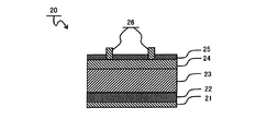
光吸収層となるp型の第1の半導体層としてSiを用いても同様な効果が得られる。図2を参照しながら本発明にかかる太陽電池の他の一例について説明する。図2に示すSi太陽電池20は、導電層21、第2の半導体層22、第1の半導体層23、n型半導体層24および表面層25を備えている。各要素は、上記の順番で積層されている。n型半導体層24上には、一部が表面層25から露出するように、表面取り出し電極26が設けられている。第1の半導体層23および第2の半導体層22の導電型は、いずれもp型である。
(Second Embodiment)
The same effect can be obtained even when Si is used as the p-type first semiconductor layer to be the light absorption layer. Another example of the solar cell according to the present invention will be described with reference to FIG. The Si
裏面電極となる導電層21としては、例えば、Alを用いることができる。第2の半導体層22としては、第1実施形態で説明した材料を用いることができる。光吸収層となる第1の半導体層23としては、例えば、Bをドープしたp型の単結晶Siや多結晶Siを用いることができる。第1の半導体層23に対して、pn接合の相手となるn型半導体層24として、例えば、Pをドープした単結晶Siや多結晶Siを用いることができる。表面再結合を低減し、かつ光反射を低減する表面層25(反射防止膜)としては、例えば、SiO2やSiNが用いられる。表面取り出し電極26として、例えば、Agが用いられる。
As the
本実施形態のSi太陽電池20において、第1の半導体層23がSiで構成される場合、その禁制帯幅Eg1は約1.1eVとなる。従って、第2の半導体層22には、禁制帯幅Eg2がそれ(Eg1)より大きくなる材料、例えば、Cu2O(Eg2=2.2eV)、Ag2O(Eg2=1.5eV)、GaN(Eg2=3.5eV)等を適宜選択すればよい。第1の半導体層24と第2の半導体層22とのヘテロ接合により、内部電界(バックサーフェスフィールド)が生じ、Si太陽電池20の変換効率が向上する。
In the Si
Si太陽電池20では、第1の半導体層23が基板を兼ねている。Si基板を200μm以下に薄板化した場合、従来のSi太陽電池では、バックサーフェスフィールドを形成するためにSi基板の裏面にAlを拡散する工程で基板に反りが生じ、その後の工程で基板が破損する恐れがあった。
In the Si
これに対し、本発明のSi太陽電池20によれば、バックサーフェスフィールドを形成するための第2の半導体層22として、Siと異なる材料を用いることが可能であり、低温で形成できる好適な材料を選択できるため、基板の反りを抑制し、太陽電池の製造の歩留まり向上を図ることができる。
On the other hand, according to the Si
(実施例1)
図1で説明した薄膜太陽電池10を以下に示す方法で製造した。
厚さ0.5mmのステンレス基板の表面を厚さ0.3mmのガラス膜で被覆し、これを基板11とした。
(Example 1)
The thin film
The surface of a stainless steel substrate having a thickness of 0.5 mm was covered with a glass film having a thickness of 0.3 mm.
ガラス膜の上に、スパッタ法により、裏面電極となる第1の導電層としてMo膜を約0.4μmの厚さで堆積させた。スパッタは、Moをターゲットとして、Arガス雰囲気中でDC1kWを印加することにより行った。さらに、Mo膜の上に第2の導電層として、Cr膜を約0.1μmの厚さで堆積させた。Cr膜は、金属Crを蒸着源として電子ビーム蒸着により形成した。 On the glass film, a Mo film having a thickness of about 0.4 μm was deposited as a first conductive layer serving as a back electrode by sputtering. Sputtering was performed by applying DC 1 kW in an Ar gas atmosphere using Mo as a target. Furthermore, a Cr film having a thickness of about 0.1 μm was deposited on the Mo film as a second conductive layer. The Cr film was formed by electron beam evaporation using metal Cr as an evaporation source.
次に、Mo膜およびCr膜からなる導電層12の上に、第2の半導体層13として、Cu2O膜を形成した。Cu2O膜の形成法の一例は以下の通りである。はじめに、金属Cuをターゲットとして、90%のArと10%のO2雰囲気中で高周波パワー200Wを印加してスパッタを行い、CuO膜を形成した。次に、このCuO膜を真空中で400℃、30分加熱してCu2O膜を形成した。
Next, a Cu 2 O film was formed as the
光吸収層となる第1の半導体層14として、CIGS膜を蒸着法により形成した。蒸着は、Cu、In、Ga、Seの各蒸発源からの蒸着レートを制御して、最高基板温度550℃で行った。形成したCIGS膜の厚さは約2μmであった。形成したCIGS膜の組成比Ga/(In+Ga)は約0.3であった。
As the
次に、窓層15として、複層の半導体膜を形成した。まず、約70nmの厚さのCdS膜を化学析出法により堆積させた。化学析出法は、硝酸Cd、チオ尿素およびアンモニアを含む水溶液を約80℃に温め、CIGS膜を上記水溶液に浸漬することにより行った。さらに、CdS膜の上に約80nmの厚さのZnO膜をスパッタ法で形成した。スパッタ法は、ZnO焼結体をターゲットとして、Arガス雰囲気中でRF400Wを印加することにより行った。
Next, a multilayer semiconductor film was formed as the
次に、スパッタ法により、透明導電膜16として、ITO膜を約150nmの厚さで堆積させた。スパッタは、SnO2を10wt%含有したITO焼結体をターゲットに用い、Arの雰囲気中でRF400Wを印加することにより行った。
Next, an ITO film having a thickness of about 150 nm was deposited as the transparent
最後に、取り出し電極17として、NiCrとAuの積層膜を電子ビーム蒸着法で形成した。NiCrとAuの厚さは各々50nmと300nmであった。 Finally, a NiCr and Au laminated film was formed as an extraction electrode 17 by an electron beam evaporation method. The thicknesses of NiCr and Au were 50 nm and 300 nm, respectively.
以上のようにして、Cu2O層の厚さが10nmのCIGS薄膜太陽電池と、Cu2O層の厚さが200nmのCIGS薄膜太陽電池とを製造した。比較のために、Cu2O層を有さないCIGS薄膜太陽電池も製造した。なお、比較例のCIGS薄膜太陽電池では、裏面電極となる導電層として、基板上にMo膜のみを堆積させた。 As described above, the CIGS thin film solar cell thickness 10nm of Cu 2 O layer, the thickness of the Cu 2 O layer was prepared and a CIGS thin film solar cell 200 nm. For comparison, a CIGS thin film solar cell having no Cu 2 O layer was also manufactured. In the CIGS thin film solar cell of the comparative example, only the Mo film was deposited on the substrate as the conductive layer to be the back electrode.
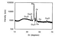
一方、Cu2O膜の結晶構造を調べるために、Cr/Mo電極上に形成されたCu2O膜のX線回折を測定した。図3にCuをX線源として測定したX線回折パターンを示す。Mo、Crおよび一部Cu以外は全てCu2Oで指数づけられる回折ピークとなっており、CuO相は存在しないことがわかる。Cuの回折ピークは、CuO膜を真空中で加熱する過程で、還元が促進し、Cu2OからCuに変化した結果である。Cr/Mo電極膜とCu2O膜との積層膜を塩酸でエッチングしたところ、Cu2O膜が除去され、Cr電極の上に薄いCu層が存在することが確認された。従って、製造した薄膜太陽電池では、第2の半導体層13としてのCu2O膜と、Cu/Cr/Mo積層膜からなる導電層12とが積層されている。
Meanwhile, in order to examine the crystal structure of the Cu 2 O film were measured X-ray diffraction of the Cu 2 O film formed on the Cr / Mo electrodes. FIG. 3 shows an X-ray diffraction pattern measured using Cu as an X-ray source. All except Mo, Cr, and some Cu are diffraction peaks indexed by Cu 2 O, and it can be seen that there is no CuO phase. The Cu diffraction peak is a result of the reduction of Cu 2 O to Cu in the process of heating the CuO film in a vacuum, with the reduction being promoted. When the laminated film of the Cr / Mo electrode film and the Cu 2 O film was etched with hydrochloric acid, the Cu 2 O film was removed, and it was confirmed that a thin Cu layer was present on the Cr electrode. Therefore, in the manufactured thin film solar cell, the Cu 2 O film as the
次に、Cu2O膜の禁制帯幅を調べるために、ガラス基板上にCu2O膜を先に説明したのと同様な工程で形成し、光透過特性を測定した。図4に光透過特性から算出した光吸収係数αとフォトンエネルギーhνの積の2乗の、フォトンエネルギーhνに対する変化を示す。切片からCu2O膜の禁制帯幅は約2.2eVであった。製造した薄膜太陽電池に用いたCIGS膜の禁制帯幅はフォトルミネッセンス測定から約1.1eVであり、光吸収層となる第1の半導体層(CIGS膜)より第2の半導体層(Cu2O膜)の禁制帯幅が大きいことを確認した。 Next, in order to examine the bandgap of the Cu 2 O film, a Cu 2 O layer on a glass substrate was formed in the same process as described above, were measured light transmission characteristics. FIG. 4 shows the change of the square of the product of the light absorption coefficient α and the photon energy hν calculated from the light transmission characteristics with respect to the photon energy hν. From the section, the forbidden band width of the Cu 2 O film was about 2.2 eV. The forbidden band width of the CIGS film used for the manufactured thin film solar cell is about 1.1 eV from the photoluminescence measurement, and the second semiconductor layer (Cu 2 O) from the first semiconductor layer (CIGS film) serving as the light absorption layer. It was confirmed that the forbidden bandwidth of the film was large.
また、同様の方法でガラス上に形成したCu2O膜を用い、Cu2O膜の電気特性を調べた。ゼーベック効果を調べたところ、Cu2O膜がp型半導体であることが確認できた。また、抵抗率の測定から、Cu2O膜の抵抗率は10Ω・cmであった。CIGS膜の抵抗率は100Ω・cmであり、光吸収層となる第1の半導体層(CIGS膜)より第2の半導体層(Cu2O膜)の抵抗率が小さいことを確認した。また、Cu2O膜とCIGS膜の抵抗率からキャリア濃度は、各々1017〜1018/cm3と1015〜1016/cm3であり、光吸収層となる第1の半導体層(CIGS膜)より第2の半導体層(Cu2O膜)のキャリア濃度が高いことを確認した。 Further, using the Cu 2 O film formed on the glass in the same manner, it was investigated the electrical properties of Cu 2 O layer. When the Seebeck effect was examined, it was confirmed that the Cu 2 O film was a p-type semiconductor. From the measurement of resistivity, the resistivity of the Cu 2 O film was 10 Ω · cm. The resistivity of the CIGS film was 100 Ω · cm, and it was confirmed that the resistivity of the second semiconductor layer (Cu 2 O film) was smaller than that of the first semiconductor layer (CIGS film) serving as the light absorption layer. Further, the carrier concentrations are 10 17 to 10 18 / cm 3 and 10 15 to 10 16 / cm 3 from the resistivity of the Cu 2 O film and the CIGS film, respectively, and the first semiconductor layer (CIGS) serving as the light absorption layer. It was confirmed that the carrier concentration of the second semiconductor layer (Cu 2 O film) was higher than that of the film.
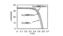
次に、製造した薄膜太陽電池に、疑似太陽光(1kW/m2, AM1.5)を照射し、電流−電圧特性を測定した。結果を図5に示す。Cu2O膜なしの比較例の薄膜太陽電池に比べ、Cu2O膜が10nmの薄膜太陽電池では開放電圧Voc(横軸)が増加している。さらに、Cu2O膜が200nmの薄膜太陽電池では、開放電圧Vocと短絡電流密度Jsc(縦軸)がともに増加している。第2の半導体層であるCu2O膜を備えることにより、裏面電極での再結合が低減し、オーミック接触が改善されることによりVocとJscが増加したと考えられる。Cu2O膜なしの薄膜太陽電池の変換効率13.1%に対し、厚さ200nmのCu2O膜を具備した薄膜太陽電池では変換効率が14.8%に向上した。 Next, the manufactured thin-film solar cell was irradiated with pseudo-sunlight (1 kW / m 2 , AM1.5), and current-voltage characteristics were measured. The results are shown in FIG. Compared with the thin-film solar battery of Comparative Example without Cu 2 O film, Cu 2 O layer is open-circuit voltage Voc is a thin-film solar cell of 10 nm (horizontal axis) is increased. Further, in a thin film solar cell having a Cu 2 O film of 200 nm, both the open circuit voltage Voc and the short circuit current density Jsc (vertical axis) are increased. By providing the Cu 2 O film as the second semiconductor layer, it is considered that recombination at the back electrode is reduced and Voc and Jsc are increased by improving the ohmic contact. To the conversion efficiency of 13.1% of the thin-film solar cell without Cu 2 O film, the conversion efficiency of a thin film solar cell provided with the Cu 2 O film having a thickness of 200nm was improved to 14.8%.
なお、Cu2O膜の厚さが10nmの薄膜太陽電池であっても、Cu2O膜なしの薄膜太陽電池に比べ、開放電圧が増加し、変換効率は0.6%向上した。第2の半導体層が太陽電池にもたらす効果は、膜厚とキャリア濃度の積に左右される。従って、本実施例のCu2Oより1桁以上低抵抗な半導体を用いるならば膜厚10nmでも十分な効果が得られる。つまり、第2の半導体層として、CuO、Ag2O、NiO、Fe2O3、CuAlO2、CuGaO2、CuInO2のp型酸化物薄膜やGaN、AlN、InNのp型窒化物薄膜やAg2S、CuS、Cu2S、NiS、FeS、FeS2のp型硫化物薄膜や、また、(Cu,Ag)2OやCu(Al,Ga)O2や(Ga,In)Nや(Cu,Ag)2S等の固溶体からなる群のうち、好適な禁制帯幅と、好適なキャリア濃度または抵抗率とを有する材料を選んで用いることにより、厚さ200nmのCu2O膜の場合と同様な結果が得られる。 Even in the case of a thin film solar cell having a Cu 2 O film thickness of 10 nm, the open-circuit voltage increased and the conversion efficiency was improved by 0.6% compared to the thin film solar cell without the Cu 2 O film. The effect of the second semiconductor layer on the solar cell depends on the product of the film thickness and the carrier concentration. Therefore, a sufficient effect can be obtained even with a film thickness of 10 nm if a semiconductor whose resistance is one digit or more lower than that of Cu 2 O of this embodiment is used. That is, as the second semiconductor layer, a p-type oxide thin film of CuO, Ag 2 O, NiO, Fe 2 O 3 , CuAlO 2 , CuGaO 2 , CuInO 2 , a p-type nitride thin film of GaN, AlN, InN or Ag 2 S, CuS, Cu 2 S, NiS, FeS, FeS 2 p-type sulfide thin film, (Cu, Ag) 2 O, Cu (Al, Ga) O 2 , (Ga, In) N, ( In the case of a Cu 2 O film having a thickness of 200 nm by selecting and using a material having a suitable forbidden band width and a suitable carrier concentration or resistivity from the group consisting of solid solutions such as Cu, Ag) 2 S, etc. Similar results are obtained.
なお、本実施例では、裏面電極となる導電層として、Cu/Cr/Mo積層膜を用いたが、Moを使用しないCu/Crを用いても同様な結果が得られる。Crの抵抗率を改善するために、Cu/Cr/Mo積層膜におけるMoの代わりに、Ti、Cu等を用いても同様な結果が得られる。 In this example, a Cu / Cr / Mo laminated film was used as the conductive layer serving as the back electrode. However, similar results can be obtained even when Cu / Cr not using Mo is used. In order to improve the resistivity of Cr, similar results can be obtained by using Ti, Cu or the like instead of Mo in the Cu / Cr / Mo laminated film.
(実施例2)
図2で説明したSi太陽電池20は、以下に示す方法で製造することができる。
p型Si単結晶基板の第1主面(表面)からPを拡散させて表層部を補償し、n型半導体層24を形成する。次に、n型半導体層24の上に、反射防止膜25としてのSiN膜を、例えばCVD法によって形成する。SiN膜の上にAgペーストを印刷し、印刷したAgペーストを焼結することによって、パターン化した表面取り出し電極26を形成する。焼結によりAgがSiN膜内を通じてSi表面へ拡散し、表面取り出し電極26とn型Si半導体層24とのオーミック接触が形成される。一方、第2主面(裏面)に、実施例1と同様の方法で、第2の半導体層22としてのCu2O膜を堆積させ、さらに、その第2の半導体層22の上に、Alペーストを印刷し、印刷したAlペーストを焼結することにより、裏面電極としてのAl層21を形成する。以上のようにして、図2で説明したSi太陽電池20を製造することができる。もちろん、Si単結晶基板に代えて、Si多結晶基板を用いてもよい。
(Example 2)
The Si
P is diffused from the first main surface (surface) of the p-type Si single crystal substrate to compensate the surface layer portion, and the n-type semiconductor layer 24 is formed. Next, a SiN film as the
10 薄膜太陽電池
11 基板
12 裏面電極(Mo膜)
13 第2の半導体層(Cu2O膜)
14 第1の半導体層(CIGS膜)
15 窓層(CdS/ZnO積層膜)
16 透明導電膜(ITO膜)
17a 裏面取り出し電極(NiCr/Au積層膜)
17b 表面取り出し電極(NiCr/Au積層膜)
20 Si太陽電池
21 裏面電極(Al層)
22 第2の半導体層
23 第1の半導体層(B添加Si層)
24 n型半導体層(P添加Si層)
25 反射防止膜(SiO2膜)
26 表面取り出し電極(Ag)
10 Thin
13 Second semiconductor layer (Cu 2 O film)
14 First semiconductor layer (CIGS film)
15 Window layer (CdS / ZnO laminated film)
16 Transparent conductive film (ITO film)
17a Back surface extraction electrode (NiCr / Au laminated film)
17b Surface extraction electrode (NiCr / Au laminated film)
20 Si
22
24 n-type semiconductor layer (P-added Si layer)
25 Antireflection film (SiO 2 film)
26 Surface extraction electrode (Ag)
Claims (12)
前記第1の半導体層は、前記第2の半導体層よりも光入射側に位置する光吸収層であり、
前記第1の半導体層と前記第2の半導体層の結晶構造が異なり、
前記第1の半導体層の禁制帯幅Eg1と前記第2の半導体層の禁制帯幅Eg2とが、Eg1<Eg2の関係を満たす、太陽電池。 A solar cell comprising a first semiconductor layer having a p-type conductivity, a second semiconductor layer having a p-type conductivity, and a conductive layer as a back electrode, wherein each layer is laminated in this order. ,
The first semiconductor layer is a light absorption layer located on the light incident side with respect to the second semiconductor layer,
The crystal structures of the first semiconductor layer and the second semiconductor layer are different,
The first forbidden band of the semiconductor layer width Eg 1 and the forbidden band width Eg 2 of the second semiconductor layer satisfies the relationship of Eg 1 <Eg 2, the solar cell.
前記第2の半導体層が、酸化銅からなる、請求項1記載の太陽電池。 The first semiconductor layer is made of a chalcopyrite structure semiconductor containing Cu, In and Se;
The solar cell according to claim 1, wherein the second semiconductor layer is made of copper oxide.
Priority Applications (1)
| Application Number | Priority Date | Filing Date | Title |
|---|---|---|---|
| JP2006165614A JP2007335625A (en) | 2006-06-15 | 2006-06-15 | Solar cell |
Applications Claiming Priority (1)
| Application Number | Priority Date | Filing Date | Title |
|---|---|---|---|
| JP2006165614A JP2007335625A (en) | 2006-06-15 | 2006-06-15 | Solar cell |
Publications (2)
| Publication Number | Publication Date |
|---|---|
| JP2007335625A true JP2007335625A (en) | 2007-12-27 |
| JP2007335625A5 JP2007335625A5 (en) | 2010-08-26 |
Family
ID=38934803
Family Applications (1)
| Application Number | Title | Priority Date | Filing Date |
|---|---|---|---|
| JP2006165614A Pending JP2007335625A (en) | 2006-06-15 | 2006-06-15 | Solar cell |
Country Status (1)
| Country | Link |
|---|---|
| JP (1) | JP2007335625A (en) |
Cited By (11)
| Publication number | Priority date | Publication date | Assignee | Title |
|---|---|---|---|---|
| JPH0486989A (en) * | 1990-07-31 | 1992-03-19 | Sanyo Electric Co Ltd | Drink vending machine |
| WO2011155639A1 (en) * | 2010-06-11 | 2011-12-15 | 昭和シェル石油株式会社 | Thin-film solar battery |
| JP2012038783A (en) * | 2010-08-03 | 2012-02-23 | Gifu Univ | Photoelectric conversion element |
| WO2012060096A1 (en) | 2010-11-02 | 2012-05-10 | 富士フイルム株式会社 | Photoelectric conversion element |
| CN102484164A (en) * | 2010-03-05 | 2012-05-30 | 株式会社东芝 | Compound thin-film solar cell and method for producing same |
| JP2013016848A (en) * | 2012-09-14 | 2013-01-24 | Sharp Corp | Semiconductor, p-type semiconductor, semiconductor bonding element, pn-junction element, and photoelectric converter |
| WO2014103239A1 (en) * | 2012-12-25 | 2014-07-03 | Sony Corporation | Solid-state image pickup device and electronic apparatus |
| EP2999007A1 (en) * | 2014-09-19 | 2016-03-23 | Kabushiki Kaisha Toshiba | Photoelectric conversion device, and solar cell |
| WO2016152857A1 (en) * | 2015-03-25 | 2016-09-29 | 京セラ株式会社 | Photoelectric conversion device |
| EP2533298A4 (en) * | 2010-10-05 | 2018-02-21 | LG Innotek Co., Ltd. | Photovoltaic device and method for manufacturing same |
| JP2022505688A (en) * | 2018-10-26 | 2022-01-14 | アプライド マテリアルズ インコーポレイテッド | Extreme UV mask with back coating |
Citations (7)
| Publication number | Priority date | Publication date | Assignee | Title |
|---|---|---|---|---|
| JPS61502020A (en) * | 1984-04-27 | 1986-09-11 | マサチュ−セッツ・インステチュ−ト・オブ・テクノロジ− | Solar cells and photodetectors |
| JPH03166770A (en) * | 1989-11-27 | 1991-07-18 | Canon Inc | Photovoltaic element |
| JPH04298081A (en) * | 1991-03-27 | 1992-10-21 | Tonen Corp | Manufacture of bsf type solar cell |
| JPH11168227A (en) * | 1997-12-02 | 1999-06-22 | Ricoh Co Ltd | Photovoltaic device and manufacture thereof |
| JPH11177112A (en) * | 1997-12-09 | 1999-07-02 | Ricoh Co Ltd | Photovoltaic device and its manufacture |
| WO2005088731A1 (en) * | 2004-03-11 | 2005-09-22 | Solibro Ab | Thin film solar cell and manufacturing method |
| JP2006013028A (en) * | 2004-06-24 | 2006-01-12 | National Institute Of Advanced Industrial & Technology | Compound solar cell and its manufacturing method |
-
2006
- 2006-06-15 JP JP2006165614A patent/JP2007335625A/en active Pending
Patent Citations (7)
| Publication number | Priority date | Publication date | Assignee | Title |
|---|---|---|---|---|
| JPS61502020A (en) * | 1984-04-27 | 1986-09-11 | マサチュ−セッツ・インステチュ−ト・オブ・テクノロジ− | Solar cells and photodetectors |
| JPH03166770A (en) * | 1989-11-27 | 1991-07-18 | Canon Inc | Photovoltaic element |
| JPH04298081A (en) * | 1991-03-27 | 1992-10-21 | Tonen Corp | Manufacture of bsf type solar cell |
| JPH11168227A (en) * | 1997-12-02 | 1999-06-22 | Ricoh Co Ltd | Photovoltaic device and manufacture thereof |
| JPH11177112A (en) * | 1997-12-09 | 1999-07-02 | Ricoh Co Ltd | Photovoltaic device and its manufacture |
| WO2005088731A1 (en) * | 2004-03-11 | 2005-09-22 | Solibro Ab | Thin film solar cell and manufacturing method |
| JP2006013028A (en) * | 2004-06-24 | 2006-01-12 | National Institute Of Advanced Industrial & Technology | Compound solar cell and its manufacturing method |
Cited By (20)
| Publication number | Priority date | Publication date | Assignee | Title |
|---|---|---|---|---|
| JPH0486989A (en) * | 1990-07-31 | 1992-03-19 | Sanyo Electric Co Ltd | Drink vending machine |
| CN102484164A (en) * | 2010-03-05 | 2012-05-30 | 株式会社东芝 | Compound thin-film solar cell and method for producing same |
| WO2011155639A1 (en) * | 2010-06-11 | 2011-12-15 | 昭和シェル石油株式会社 | Thin-film solar battery |
| JP2011258858A (en) * | 2010-06-11 | 2011-12-22 | Showa Shell Sekiyu Kk | Thin film solar cell |
| US9166077B2 (en) | 2010-06-11 | 2015-10-20 | Solar Frontier K. K. | Thin film solar cell |
| JP2012038783A (en) * | 2010-08-03 | 2012-02-23 | Gifu Univ | Photoelectric conversion element |
| EP2533298A4 (en) * | 2010-10-05 | 2018-02-21 | LG Innotek Co., Ltd. | Photovoltaic device and method for manufacturing same |
| WO2012060096A1 (en) | 2010-11-02 | 2012-05-10 | 富士フイルム株式会社 | Photoelectric conversion element |
| JP2013016848A (en) * | 2012-09-14 | 2013-01-24 | Sharp Corp | Semiconductor, p-type semiconductor, semiconductor bonding element, pn-junction element, and photoelectric converter |
| WO2014103239A1 (en) * | 2012-12-25 | 2014-07-03 | Sony Corporation | Solid-state image pickup device and electronic apparatus |
| CN104854700A (en) * | 2012-12-25 | 2015-08-19 | 索尼公司 | Solid-state image pickup device and electronic apparatus |
| US9515208B2 (en) | 2012-12-25 | 2016-12-06 | Sony Corporation | Solid-state image pickup device and electronic apparatus |
| CN104854700B (en) * | 2012-12-25 | 2018-06-12 | 索尼公司 | Solid-state image pickup device and electronic equipment |
| EP2999007A1 (en) * | 2014-09-19 | 2016-03-23 | Kabushiki Kaisha Toshiba | Photoelectric conversion device, and solar cell |
| JP2016063160A (en) * | 2014-09-19 | 2016-04-25 | 株式会社東芝 | Photoelectric conversion element and solar cell |
| CN105449009A (en) * | 2014-09-19 | 2016-03-30 | 株式会社东芝 | Photoelectric conversion device, and solar cell |
| WO2016152857A1 (en) * | 2015-03-25 | 2016-09-29 | 京セラ株式会社 | Photoelectric conversion device |
| JPWO2016152857A1 (en) * | 2015-03-25 | 2017-12-28 | 京セラ株式会社 | Photoelectric conversion device |
| JP2022505688A (en) * | 2018-10-26 | 2022-01-14 | アプライド マテリアルズ インコーポレイテッド | Extreme UV mask with back coating |
| JP7288959B2 (en) | 2018-10-26 | 2023-06-08 | アプライド マテリアルズ インコーポレイテッド | Extreme UV mask with backside coating |
Similar Documents
| Publication | Publication Date | Title |
|---|---|---|
| JP2007335625A (en) | Solar cell | |
| KR101503557B1 (en) | Photovoltaic devices including an interfacial layer | |
| US8916767B2 (en) | Solar cell and method of fabricating the same | |
| JP6096790B2 (en) | Conductive substrate for photovoltaic cells | |
| EP1492169A2 (en) | Solar cell | |
| US20080023059A1 (en) | Tandem solar cell structures and methods of manufacturing same | |
| US20110315220A1 (en) | Photovoltaic cell and methods for forming a back contact for a photovoltaic cell | |
| US8871560B2 (en) | Plasma annealing of thin film solar cells | |
| KR101893411B1 (en) | A preparation method of solar cell using ZnS buffer layer | |
| JP4394366B2 (en) | Double-sided solar cell | |
| EP2426731A2 (en) | Solar power generation apparatus and manufacturing method thereof | |
| EP2485272A2 (en) | Solar power generation apparatus and manufacturing method thereof | |
| CN104011875A (en) | Solar cell and method of fabricating same | |
| US20130029450A1 (en) | Method for manufacturing solar cell | |
| US20140000673A1 (en) | Photovoltaic device and method of making | |
| JP4975528B2 (en) | Integrated solar cell | |
| JP5465860B2 (en) | Photovoltaic element and manufacturing method thereof | |
| CN104810429A (en) | Method of making photovoltaic device comprising an absorber having a surface layer | |
| EP3300122A1 (en) | Material structure for a solar cell and a solar cell comprising the material structure | |
| JP5701673B2 (en) | Photoelectric conversion element and solar cell | |
| KR20110013009A (en) | Photovoltaic device including plural back contact metal layers and manufacturing method thereof | |
| EP3903352B1 (en) | Photovoltaic devices and methods of forming the same | |
| US20140060608A1 (en) | Photovoltaic device and method of making | |
| KR20150115363A (en) | Method of manufacturing solar cell having CI(G)S based light absorption layer | |
| KR101924538B1 (en) | Chalcogenide solar cell having a transparent conductive oxide back electrode and method for manufacturing the same |
Legal Events
| Date | Code | Title | Description |
|---|---|---|---|
| A521 | Request for written amendment filed |
Free format text: JAPANESE INTERMEDIATE CODE: A523 Effective date: 20090520 |
|
| A621 | Written request for application examination |
Free format text: JAPANESE INTERMEDIATE CODE: A621 Effective date: 20090520 |
|
| A521 | Request for written amendment filed |
Free format text: JAPANESE INTERMEDIATE CODE: A523 Effective date: 20100709 |
|
| A977 | Report on retrieval |
Free format text: JAPANESE INTERMEDIATE CODE: A971007 Effective date: 20101228 |
|
| A131 | Notification of reasons for refusal |
Free format text: JAPANESE INTERMEDIATE CODE: A131 Effective date: 20110517 |
|
| A521 | Request for written amendment filed |
Free format text: JAPANESE INTERMEDIATE CODE: A523 Effective date: 20110715 |
|
| A131 | Notification of reasons for refusal |
Free format text: JAPANESE INTERMEDIATE CODE: A131 Effective date: 20120515 |
|
| A521 | Request for written amendment filed |
Free format text: JAPANESE INTERMEDIATE CODE: A523 Effective date: 20120717 |
|
| A02 | Decision of refusal |
Free format text: JAPANESE INTERMEDIATE CODE: A02 Effective date: 20130305 |