WO2012056929A1 - 表示装置 - Google Patents
表示装置 Download PDFInfo
- Publication number
- WO2012056929A1 WO2012056929A1 PCT/JP2011/073838 JP2011073838W WO2012056929A1 WO 2012056929 A1 WO2012056929 A1 WO 2012056929A1 JP 2011073838 W JP2011073838 W JP 2011073838W WO 2012056929 A1 WO2012056929 A1 WO 2012056929A1
- Authority
- WO
- WIPO (PCT)
- Prior art keywords
- light
- display device
- housing
- light source
- liquid crystal
- Prior art date
- Legal status (The legal status is an assumption and is not a legal conclusion. Google has not performed a legal analysis and makes no representation as to the accuracy of the status listed.)
- Ceased
Links
Images





Classifications
-
- G—PHYSICS
- G02—OPTICS
- G02F—OPTICAL DEVICES OR ARRANGEMENTS FOR THE CONTROL OF LIGHT BY MODIFICATION OF THE OPTICAL PROPERTIES OF THE MEDIA OF THE ELEMENTS INVOLVED THEREIN; NON-LINEAR OPTICS; FREQUENCY-CHANGING OF LIGHT; OPTICAL LOGIC ELEMENTS; OPTICAL ANALOGUE/DIGITAL CONVERTERS
- G02F1/00—Devices or arrangements for the control of the intensity, colour, phase, polarisation or direction of light arriving from an independent light source, e.g. switching, gating or modulating; Non-linear optics
- G02F1/01—Devices or arrangements for the control of the intensity, colour, phase, polarisation or direction of light arriving from an independent light source, e.g. switching, gating or modulating; Non-linear optics for the control of the intensity, phase, polarisation or colour
- G02F1/13—Devices or arrangements for the control of the intensity, colour, phase, polarisation or direction of light arriving from an independent light source, e.g. switching, gating or modulating; Non-linear optics for the control of the intensity, phase, polarisation or colour based on liquid crystals, e.g. single liquid crystal display cells
- G02F1/133—Constructional arrangements; Operation of liquid crystal cells; Circuit arrangements
- G02F1/1333—Constructional arrangements; Manufacturing methods
- G02F1/1335—Structural association of cells with optical devices, e.g. polarisers or reflectors
- G02F1/1336—Illuminating devices
- G02F1/133602—Direct backlight
- G02F1/133603—Direct backlight with LEDs
-
- G—PHYSICS
- G02—OPTICS
- G02F—OPTICAL DEVICES OR ARRANGEMENTS FOR THE CONTROL OF LIGHT BY MODIFICATION OF THE OPTICAL PROPERTIES OF THE MEDIA OF THE ELEMENTS INVOLVED THEREIN; NON-LINEAR OPTICS; FREQUENCY-CHANGING OF LIGHT; OPTICAL LOGIC ELEMENTS; OPTICAL ANALOGUE/DIGITAL CONVERTERS
- G02F1/00—Devices or arrangements for the control of the intensity, colour, phase, polarisation or direction of light arriving from an independent light source, e.g. switching, gating or modulating; Non-linear optics
- G02F1/01—Devices or arrangements for the control of the intensity, colour, phase, polarisation or direction of light arriving from an independent light source, e.g. switching, gating or modulating; Non-linear optics for the control of the intensity, phase, polarisation or colour
- G02F1/13—Devices or arrangements for the control of the intensity, colour, phase, polarisation or direction of light arriving from an independent light source, e.g. switching, gating or modulating; Non-linear optics for the control of the intensity, phase, polarisation or colour based on liquid crystals, e.g. single liquid crystal display cells
- G02F1/133—Constructional arrangements; Operation of liquid crystal cells; Circuit arrangements
- G02F1/1333—Constructional arrangements; Manufacturing methods
- G02F1/1335—Structural association of cells with optical devices, e.g. polarisers or reflectors
- G02F1/1336—Illuminating devices
- G02F1/133618—Illuminating devices for ambient light
Definitions
- the present invention relates to a display device such as a liquid crystal display device.
- the liquid crystal display panel that displays images does not emit light.
- the back surface of a liquid crystal display panel is illuminated with the light from the illuminating device.
- the illuminating device installed in the back surface side of a liquid crystal display panel is called the backlight unit etc., for example.
- a cold cathode fluorescent lamp in which mercury or xenon is enclosed in a fluorescent tube is known.
- the cold cathode fluorescent lamp is used as the light source of the backlight unit, there are disadvantages that the light emission luminance and life are insufficient, and that the luminance on the low-pressure side is low, making it difficult to obtain a uniform light emission. It was. Therefore, in order to eliminate such inconvenience, various backlight units using an LED (light emitting diode) package as a light source have been proposed in place of the cold cathode fluorescent lamp.
- the backlight unit is roughly classified into two types, an edge light type and a direct type.
- An edge-light type backlight unit has a light guide plate arranged directly under a liquid crystal display panel (a region facing the back surface of the liquid crystal display panel), and a light source arranged so as to face a predetermined side end surface of the light guide plate. It is.
- the edge light type backlight unit when light is emitted from the light source, the light from the light source is introduced into the light guide plate through a predetermined side end surface of the light guide plate. Then, the light introduced into the light guide plate is emitted from the front surface of the light guide plate (the surface directed toward the liquid crystal display panel), so that the back surface of the liquid crystal display panel is illuminated.
- the direct type backlight unit has a light source arranged directly under the liquid crystal display panel.
- a direct type backlight unit is advantageous for illuminating a large area with high output, and is often used for a large-sized liquid crystal display device.
- a direct-type backlight unit using an LED package as a light source is disclosed in, for example, Patent Document 1.
- liquid crystal display device that can appear as if an image is being displayed.
- a projection surface on the back side of the liquid crystal display device is used to project light having a hue corresponding to an image displayed on the liquid crystal display panel onto the projection surface on the back side of the liquid crystal display device.
- a dedicated light source for generating projection light onto the back of the liquid crystal display device is separately mounted.
- a dedicated light source for generating projection light onto the projection surface on the back side of the liquid crystal display device is separately mounted on the back surface portion of the liquid crystal display device, so that it is displayed on the liquid crystal display panel.
- the number of parts (number of light sources used) increases and power consumption (drives the light source)
- the power for power generation increases.
- the present invention has been made to solve the above-described problems, and suppresses an increase in the number of components and an increase in power consumption, while causing light of a hue corresponding to a displayed image to be projected onto a projection surface on the back side of the display device.
- An object is to provide a display device capable of projecting.
- a display device includes a housing having a bottom portion, and a light source that is attached to the bottom portion of the housing and emits light in a hue corresponding to an image to be displayed. .
- the light emission hole is formed in the bottom part of a housing
- a part of the light emitted from the light source is attached to the light source at the bottom of the housing through the light emission hole formed in the bottom of the housing.
- the light of the hue corresponding to the image to be displayed is projected onto the projection surface (screen, wall surface, etc.) on the back side of the display device, thereby
- a dedicated light source for generating projection light onto the projection surface on the back side of the display device is provided.
- light having a hue corresponding to the image to be displayed can be projected onto the projection surface on the back side of the display device.
- the display device further includes a display panel for displaying an image, the side facing the bottom of the housing is opened, and the display panel is disposed on the opening side of the housing,
- the light for illuminating the panel may be generated by the light source, and the hue of the light emitted from the light source may be in accordance with the image displayed on the display panel.
- the light source includes a plurality of light sources, and the plurality of light sources are two-dimensionally arranged in a predetermined portion of the bottom of the housing as viewed in plan from the side facing the bottom of the housing.
- a light emission hole is formed in an outer edge portion surrounding a light source mounting portion (a predetermined portion of the bottom portion of the casing) on which a plurality of light sources are mounted in the bottom portion of the casing.
- a plurality of light sources may be arranged in a matrix.
- a predetermined number of light source arrays each including two or more light sources may be arranged in parallel, and the light source arrangement positions may be staggered between adjacent light source arrays.
- the light emitting hole is partitioned into a plurality of light emitting holes. If comprised in this way, even if the formation area of the light emission hole with respect to the bottom part of a housing
- the display device further includes a reflection sheet disposed on the bottom of the housing and having an exposure hole for exposing the light source mounted on the bottom of the housing, the light source A light passage hole for allowing a part of the light emitted from the light to pass through is formed in the reflection sheet, and a part of the light emitted from the light source passes through the light passage hole and reaches the light emission hole. It is preferable. If comprised in this way, even if the reflection sheet is arrange
- the light passage hole is partitioned into a plurality of light passage holes.
- the display device further includes a diffusion plate disposed on a side facing the bottom of the housing, and a part of the light emitted from the light source is reflected toward the bottom of the housing by the diffusion plate. Accordingly, it is preferable that a part of the light emitted from the light source reaches the light emitting hole. If comprised in this way, a part of light emitted from the light source can be easily radiate
- the display device further includes a translucent member arranged to close the light emitting hole. If comprised in this way, even if it forms a light emission hole in the bottom part of a housing
- the optical member that performs at least one of light diffusion and condensing may be a translucent member. If comprised in this way, the light radiate
- a display capable of projecting light having a hue corresponding to a video to be displayed on the projection surface on the back side of the display device while suppressing an increase in the number of components and an increase in power consumption.
- a device can be obtained.
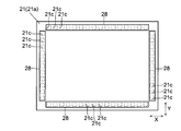
- FIG. 2 is a plan view when the back chassis (housing) of the backlight unit shown in FIG. 1 is viewed in plan view from the liquid crystal display panel side.
- FIG. 2 is a plan view when the back chassis of the backlight unit shown in FIG. 1 is viewed in plan from the back side (the side opposite to the liquid crystal display panel side).
- It is a perspective view of the reflective sheet of the backlight unit shown in FIG.
- It is a top view at the time of seeing planarly the reflective sheet of the backlight unit shown in FIG. 1 from the liquid crystal display panel side.
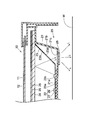
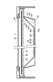
- FIG. 2 is a diagram illustrating a traveling direction of light emitted from a light emitting hole formed in a back chassis of the backlight unit illustrated in FIG. 1. It is sectional drawing of the liquid crystal display panel (display panel) with which the liquid crystal display device (display device) by 2nd Embodiment of this invention is equipped, and a backlight unit. It is sectional drawing of the liquid crystal display panel (display panel) with which the liquid crystal display device (display apparatus) by 3rd Embodiment of this invention is equipped, and a backlight unit.
- the display device is a liquid crystal display device, and as shown in FIG. 1, a liquid crystal display panel 10 for displaying an image and a back surface side opposite to the display surface side of the liquid crystal display panel 10. And at least a backlight unit 20 to be installed.
- the liquid crystal display panel 10 is an example of the “display panel” in the present invention.
- the liquid crystal display panel 10 has a display area where an image is actually displayed and a non-display area which is an outer edge area of the display area. A plurality of sub-pixels arranged in a matrix are formed in the display area of the liquid crystal display panel 10.
- Each of the plurality of sub-pixels is color-coded by, for example, one of red (R), green (G), and blue (B) colored layers, and is separated from each other by a black matrix layer.
- An aggregate including one red (R), green (G), and blue (B) subpixel is defined as one pixel. In order to make the drawing easy to see, the colored layer and the black matrix layer are not shown.
- each of the plurality of sub-pixels is driven by a switching element, a pixel electrode, a common electrode, and the like.
- the switching element, the pixel electrode, and the common electrode are not shown, and wirings that are electrically connected to them are not shown.
- the switching element is made of a TFT (thin film transistor), the gate of the switching element is connected to a gate line (scanning line), and the source of the switching element is connected to a source line (data line).
- a pixel electrode is connected to the drain of the switching element, a common electrode is disposed so as to face the pixel electrode, and a liquid crystal (not shown) is sandwiched between the pixel electrode and the common electrode.
- the switching element is individually provided for each sub-pixel, and the pixel electrode is also individually provided for each sub-pixel.
- the common electrode is common to each sub-pixel as the name implies.
- the backlight unit 20 adopts a direct type system, emits backlight light (illumination light) in a planar shape, and illuminates the back surface of the liquid crystal display panel 10 with the backlight light. ing.
- the optical property (light transmittance) of the liquid crystal is changed for each sub-pixel based on the video signal. Specifically, in each sub-pixel, electric power is generated between the pixel electrode and the common electrode by supplying power to the pixel electrode through the switching element. The orientation of the liquid crystal, that is, the transmittance of light transmitted through the liquid crystal is changed by the electric field generated between the pixel electrode and the common electrode.
- the transmission amount of the backlight light transmitted through the liquid crystal display panel 10 is different for each sub-pixel. As a result, a desired image is displayed on the liquid crystal display panel 10.
- the liquid crystal display panel 10 includes at least two transparent substrates 11 and 12.
- One transparent substrate 11 is referred to as an active matrix substrate, and the other transparent substrate 12 may be referred to as a counter substrate because it is disposed opposite to the transparent substrate 11, or a color filter.
- a switching element and a pixel electrode are formed, and a gate line (scanning line) and a source line (data line) electrically connected to them are also formed.
- a common electrode is formed on a predetermined surface of the other transparent substrate 12, and a color filter including a colored layer and a black matrix layer is formed.
- Each predetermined surface of the two transparent electrodes 11 and 12 is covered with an alignment film (not shown) capable of aligning the liquid crystal in a specific direction.
- the two transparent substrates 11 and 12 are bonded to each other via a seal material (not shown) so that their predetermined surfaces face each other.
- a liquid crystal is sealed between the two transparent substrates 11 and 12.
- the liquid crystal is sandwiched between the pixel electrode and the common electrode (between the alignment film covering the predetermined surface of one transparent substrate 11 and the alignment film covering the predetermined surface of the other transparent electrode 12). ing.
- the outer sizes of the two transparent substrates 11 and 12 are different from each other, and the outer size of the transparent substrate 11 is larger than the outer size of the transparent substrate 12. Accordingly, the two transparent substrates 11 and 12 are bonded to each other, but the predetermined ends of the transparent substrates 11 and 12 do not match each other, and a part of the predetermined surface of the transparent substrate 11 is separated from the transparent substrate 12. Exposed. The exposed portion of the predetermined surface of the transparent substrate 11 is a region of a non-display area, and is used for electrically connecting a driver (not shown) to the transparent substrate 11.
- one polarizing sheet that transmits only light waves in a specific vibration direction is provided on each of the surfaces opposite to the predetermined surface (the liquid crystal side surface) of the two transparent substrates 11 and 12. It is affixed. The transmission axis directions of the two polarizing sheets are shifted from each other by about 90 °.
- the backlight unit 20 installed on the back side of the liquid crystal display panel 10 includes at least a back chassis 21, a light source module 22, a reflection sheet 23, a diffusion plate 24, and an optical sheet 25.
- the back chassis 21 is an example of the “housing” in the present invention.
- the back chassis 21 is formed to have a substantially box-shaped accommodation area opened on the liquid crystal display panel 10 side. That is, the back chassis 21 includes a bottom portion 21a having a substantially rectangular shape in plan view (when viewed from the liquid crystal display panel 10 side), and four side portions 21b standing on the outer peripheral end of the bottom portion 21a. Have.
- the bottom portion 21 a of the back chassis 21 is a portion opposite to the opening side of the back chassis 21, and the four side portions 21 b of the back chassis 21 are obliquely raised from the outer peripheral end of the bottom portion 21 a of the back chassis 21. It is the part (the part which inclined diagonally).
- An area surrounded by the bottom 21a and the four side parts 21b of the back chassis 21 is an accommodation area.
- the light source module 22 is for generating backlight light, and is housed in the housing area of the back chassis 21 and mounted and fixed to the bottom 21a of the back chassis 21. In other words, the light source module 22 is disposed on the bottom 21 a of the back chassis 21. Thus, when the backlight unit 20 is installed on the back side of the liquid crystal display panel 10, the light source module 22 is arranged directly below the liquid crystal display panel 10 (a region facing the back side of the liquid crystal display panel 10). .
- the light source module 22 includes an LED package 26 as a light source (point light source) and an LED substrate 27 having a mounting surface on which the LED package 26 is mounted. Then, the backlight light is actually generated by the LED package 26 mounted on the mounting surface of the LED substrate 27.
- the structure of the LED package 26 is a combination of three types of LED elements that are driven independently of each other (a red LED element that emits red light, a green LED element that emits green light, and a blue LED element that emits blue light). It has become a thing. For this reason, the LED package 26 emits mixed color light obtained by mixing three colors of light with each other. Therefore, if the driving of each LED element included in the LED package 26 is adjusted separately, the light emission color of the LED package 26 (the hue of light emitted from the LED package 26) can be appropriately changed. Of course, the light emission luminance of the LED package 26 can also be changed.
- the number of LED packages 26 mounted is plural, and the plurality of LED packages 26 are viewed in a plan view from the opening side of the back chassis 21 as shown in FIG. They are arranged in a matrix at predetermined intervals in the longitudinal direction of the bottom 21a and the Y direction (the short direction of the bottom 21a of the back chassis 21).
- the display area of the liquid crystal display panel 10 (see FIG. 1) is divided into a predetermined number of display areas each including two or more pixels, and one LED package 26 is provided for each of the predetermined number of display areas. Assigned one by one. In other words, when a certain one display area of the predetermined number of display areas is described as an example, video display in the display area is performed by receiving light from the same LED package 26.
- the plurality of LED packages 26 are driven independently of each other. Therefore, the light emission color and light emission luminance of the LED package 26 are appropriately changed for each display area in accordance with the video displayed on the liquid crystal display panel 10 (see FIG. 1) (each video displayed in a predetermined number of display areas).
- (Area active drive) can be performed. By performing such area active driving, it is possible to improve contrast and reduce power consumption. In the first embodiment, area active drive is actually performed.
- the reflective sheet 23 shown in FIG. 1 is for reflecting the light emitted from the LED package 26 toward the liquid crystal display panel 10, and is housed in the housing area of the back chassis 21 together with the light source module 22. ing.
- the outer edge thereof is raised obliquely toward the opening side of the back chassis 21. That is, the reflection sheet 23 has a bottom portion 23a having a substantially rectangular shape in plan view, and four obliquely inclined side portions (outer edge portions) 23b standing on the outer peripheral end of the bottom portion 23a.
- the bottom portion 23 a of the reflection sheet 23 is placed on the bottom portion 21 a of the back chassis 21 with the LED substrate 27 interposed therebetween. That is, the bottom 23 a of the reflection sheet 23 covers the mounting surface of the LED substrate 27 (including a part of the surface of the back chassis 21 on the accommodation area side of the bottom 21 a).
- the four side portions 23b of the reflection sheet 23 respectively cover the accommodation region side surfaces of the four side portions 21b of the back chassis 21.
- the LED package 26 mounted on the LED substrate 27 is also covered with the bottom portion 23 a of the reflection sheet 23.
- an exposure hole 23 c having a circular opening shape is formed on the bottom portion 23 a of the reflection sheet 23. The same number is formed. Then, one LED package 26 is exposed (projected) to the opening side of the back chassis 21 from each of the exposed holes 23 c of the reflection sheet 23.
- the diffusing plate 24 is for introducing light emitted from the LED package 26 and diffusing and emitting the light toward the liquid crystal display panel 10 side.
- the diffusing plate 24 has a substantially rectangular front surface, a rear surface opposite to the front surface, and a front surface. And a plurality of side surfaces connected to the rear surface.
- the diffusion plate 24 is disposed so as to close the opening of the back chassis 21, the front surface of the diffusion plate 24 is directed toward the liquid crystal display panel 10, and the rear surface of the diffusion plate 24 is directed toward the bottom 21 a side of the back chassis 21. It is in the state that was. That is, the light source module 22 is covered by the diffusion plate 24 from the liquid crystal display panel 10 side.
- the light when light is emitted from the LED package 26, the light is introduced into the diffusion plate 24 from the rear surface of the diffusion plate 24.
- the light introduced into the diffusion plate 24 is diffused and emitted from the front surface of the diffusion plate 24 toward the liquid crystal display panel 10 side.
- the optical sheet 25 is a sheet group including a diffusion sheet and a lens sheet, and is disposed on the front surface of the diffusion plate 24. Thus, when light is emitted from the front surface of the diffusion plate 25, the optical sheet 25 diffuses or collects the light. Note that the type and the number of sheets used of the optical sheet 25 are appropriately changed according to the application.
- a light passage hole (slit) 23 d that allows a part of the backlight light (a part of the light emitted from the LED package 26) to pass without reflecting is formed in the reflective sheet 23. Yes. Further, a part of the backlight light that has passed through the light passage hole 23d of the reflection sheet 23 is emitted to the outside of the back chassis 21 (the side opposite to the side where the LED package 26 is mounted on the bottom 21a of the back chassis 21). A light exit hole 21 c for the purpose is formed in the back chassis 21.
- the light exit hole 21c of the back chassis 21 is formed and arranged so as to be in the state shown in FIG.
- a portion of the bottom portion 21a of the back chassis 21 that has a substantially rectangular shape in a plan view on which a plurality of LED packages 26 arranged in a matrix are mounted (enclosed by a broken line in FIG. 2).
- the portion) is referred to as a light source mounting portion P1
- a substantially frame-shaped portion in a plan view surrounding the light source mounting portion P1 is referred to as an outer edge portion P2 for distinction.
- the side portion (outer edge portion) 23b of the reflection sheet 23 overlaps with the mounting portion P1, and the outer edge portion P2 of the bottom portion 21a of the back chassis 21 in a plan view.
- the light emitting holes 21c of the back chassis 21 are formed on the bottom 21a of the back chassis 21 as shown in FIG. And arranged so as to surround the light source mounting portion P1 from four directions in plan view (along the four sides of the light source mounting portion P1).
- the light emitting holes 21c of the back chassis 21 are formed on the outer edge side of the plurality of LED packages 26 arranged in a matrix in the plan view (the LED package surrounded by the one-dot chain line in FIG. 2).
- 26 is formed and arranged along a frame-shaped LED package row, that is, an LED package group composed of a plurality of LED packages 26 arranged in a matrix is surrounded from four sides.
- the light exit hole 21c of the back chassis 21 is partitioned into two or more light exit holes 21c. That is, it can be said that the plurality of light emission holes 21 c are formed in the bottom portion 21 a of the back chassis 21.
- the diffusion sheet 28 is formed in an elongated shape (strip shape).
- the diffusion sheet 28 is disposed on each of the four sides of the bottom portion 21a of the back chassis 21.
- the light emission holes 21c described above are collectively closed by one diffusion sheet 28.
- the diffusion sheet 28 is an example of the “translucent member” and “optical member” in the present invention.
- the light passage hole 23 d of the reflection sheet 23 is formed on each of the four side portions (outer edge portions) 23 b of the reflection sheet 23, and the bottom of the reflection sheet 23 in plan view. It arrange
- the bottom 23a of the reflection sheet 23 is a portion where a plurality of exposed holes 23c are formed through which the plurality of LED packages 26 arranged in a matrix are individually exposed. For this reason, the light passage hole 23d of the reflection sheet 23 is similar to the light emission hole 21c (see FIG.
- the package package 26 is formed and arranged along a frame-shaped LED package row, that is, the LED package group composed of a plurality of LED packages 26 is surrounded from four sides.
- the light passage hole 23d of the reflection sheet 23 is partitioned into two or more light passage holes 23d. That is, it can be said that a plurality of light passage holes 23 d are formed in the four side portions 23 b of the reflection sheet 23.
- the number of light passage holes 23d formed in the reflection sheet 23 is the same as the number of light emission holes 21c (see FIG. 2) formed in the back chassis 21.
- One light passage hole 23 d of the reflection sheet 23 is assigned to each of the plurality of light emission holes 21 c of the back chassis 21.
- a part of the backlight light (a part of the light emitted from the LED package 26) is outside the back chassis 21 (the LED on the bottom 21 a of the back chassis 21).
- the light is emitted to the back side of the backlight unit 20 (the back side of the liquid crystal display device).
- an arrow L in FIG. 6 represents the traveling direction of light emitted to the outside of the back chassis 21.
- a part of the light emitted from the LED package 26 is reflected by the diffusion plate 24 without being introduced into the diffusion plate 24.
- light is repeatedly reflected between the reflection sheet 23 and the diffusing plate 24 in a region away from the side portion 23 b of the reflection sheet 23.
- the light passage hole 23d is formed in the side portion 23b of the reflection sheet 23, so that light is lost through the light passage hole 23d of the reflection sheet 23.
- not all of the side part 23b of the reflection sheet 23 is a light passage hole 23d, so that there is also light reflected by the side part 23b of the reflection sheet 23.
- the light When light passes through the light passage hole 23 d of the reflection sheet 23, the light reaches the light emission hole 21 c of the back chassis 21 and passes through the light emission hole 21 c of the back chassis 21. That is, light is emitted from the light emission hole 21 c of the back chassis 21 to the back side of the backlight unit 20. At this time, since the light exit hole 21c of the back chassis 21 is closed from the back side by the diffusion sheet 28, the light emitted from the light exit hole 21c of the back chassis 21 is diffused by the diffusion plate 28.
- the light emitted from the LED package 26 on the outer edge side occupies most of the light emitted from the light emitting hole 21 c of the back chassis 21 (however, the light on the outer edge side).
- the light emitted from the LED packages 26 other than the LED package 26 is also slightly included). For this reason, light of a hue corresponding to the image displayed mainly in the display area on the outer edge side of the display area of the liquid crystal display panel 10 is projected onto the wall surface W on the back side of the backlight unit 20. Become.
- the liquid crystal display panel 10 can be The light of the hue according to the displayed image is projected onto the wall W on the back side of the liquid crystal display device, so that the image is displayed in a display area larger than the actual display area of the liquid crystal display panel 10.
- a dedicated LED package 26 that generates projection light onto the wall W on the back side of the liquid crystal display device is separately mounted on the back surface portion of the liquid crystal display device.
- the light emitting hole 21c is formed in the outer edge portion P2 of the bottom portion 21a of the back chassis 21, so that the light emitted from the LED package 26 on the outer edge side is emitted from the back chassis 21. It becomes easy to be emitted to the outside of the back chassis 21 through the light emission hole 21c.
- light of a hue corresponding to the image displayed mainly in the display area on the outer edge side of the display area of the liquid crystal display panel 10 is projected onto the wall surface W on the back side of the liquid crystal display device. It feels like the display area on the edge has been expanded. For this reason, it is possible to make it appear that a video is displayed in a display area having a size larger than the actual display area of the liquid crystal display panel 10 without a sense of incongruity.
- the light emission holes 21c of the back chassis 21 are partitioned into a plurality of light emission holes 21c, so that the light emission holes 21c can be formed in a wide area with respect to the bottom 21a of the back chassis 21. Even if it exists, since the partition part (part between adjacent light emission holes 21c) which partitions the light emission hole 21c of the back chassis 21 into a plurality functions as a reinforcing part, the strength of the back chassis 21 is increased. It can suppress that it falls.
- the light passage hole 23d for allowing a part of the light emitted from the LED package 26 to pass therethrough is formed in the reflection sheet 23, whereby the bottom portion 21a of the back chassis 21 is formed. Even if the reflection sheet 23 is disposed, a part of the light emitted from the LED package 26 can easily reach the light emitting hole 21 c of the back chassis 21.
- the light exit hole 21c of the back chassis 21 is closed with the diffusion sheet 28, so that the light exiting from the light exit hole 21c of the back chassis 21 is diffused or condensed. Can be. Furthermore, the intrusion of foreign matter from the light exit hole 21c of the back chassis 21 can be suppressed.
- a predetermined number (two or more) of the light emission holes 21c of the back chassis 21 are not collectively covered with the diffusion sheet 28, but the number of light emission holes 21c of the back chassis 21 formed.
- the same number of diffusion sheets as (number of partitions) may be prepared, and the light emission holes 21c of the back chassis 21 may be individually closed with the diffusion sheets.
- all the light emission holes 21c of the back chassis 21 do not have to be blocked by the diffusion sheet 28 having the same diffusion rate.
- the diffusion rate of the diffusion sheet that closes the light emission holes 21c located at the four corners of the back chassis 21 may be made higher than the diffusion rate of the diffusion sheet that closes the other light emission holes 21c. In this way, the diffusion of the light emitted from the light emission holes 21c at the four corners of the back chassis 21 is further promoted. Therefore, the light projected on the wall surface W on the back side of the backlight unit 20 is diffused widely also in a region facing the four corners of the bottom 21 a of the back chassis 21.
- the light exit hole 21c of the back chassis 21 may be closed with an optical member such as a diffusion lens or a condenser lens.
- the number of light emission holes 21c (the number of partitions) in the back chassis 21 and the number of light passage holes 23d in the reflection sheet 23 (the number of partitions) may not be the same.
- the opening size of each light emission hole 21 c is increased, and the light that has passed through the two or more light passage holes 23 d of the reflection sheet 23 is mixed. You may do it.
- the number of light passage holes 23d formed in the reflection sheet 23 may be reduced.
- the light emission hole 21c is formed in the portion of the bottom portion 21a of the back chassis 21 where the stand is attached. May be omitted.
- the light emission hole 21c of the back chassis 21 is replaced by a simple transparent sheet 29 having no light diffusion function. It is blocked from the side.
- the transparent sheet 29 is an example of the “translucent member” in the present invention.
- the cost is higher than when the light emission hole 21c of the back chassis 21 is closed with a diffusion sheet. Is reduced.
- diffusion of light emitted from the light exit hole 21c of the back chassis 21 is not performed, but entry of foreign matter from the light exit hole 21c of the back chassis 21 can be suppressed.
- the light emitting hole 21 c of the back chassis 21 is not closed and is opened.
- the present invention is applied to the liquid crystal display device.
- the present invention is not limited to this, and the present invention is applied to display devices other than the liquid crystal display device (such as a display device using no display panel). May be applied.
- Liquid crystal display panel (display panel) 21 Back chassis (housing) 21a Bottom portion 21c Light exit hole 23 Reflective sheet 23c Exposed hole 23d Light passage hole 24 Diffuser plate 26 LED package (light source) 28 Diffusion sheet (translucent member, optical member) 29 Transparent sheet (translucent member) P1 Light source mounting part P2 Outer edge part
Landscapes
- Physics & Mathematics (AREA)
- Nonlinear Science (AREA)
- Liquid Crystal (AREA)
- Mathematical Physics (AREA)
- Chemical & Material Sciences (AREA)
- Crystallography & Structural Chemistry (AREA)
- General Physics & Mathematics (AREA)
- Optics & Photonics (AREA)
- Planar Illumination Modules (AREA)
Abstract
部品点数の増加および消費電力の増大を抑制しながら、表示する映像に応じた色相の光を表示装置の背面側の投影面に投影することが可能な表示装置を提供する。この表示装置は、バックシャーシ(21)と、表示される映像に応じた色相で発光するLEDパッケージ(26)とを備えている。そして、バックシャーシ(21)の底部(21a)に光出射穴(21c)が形成されており、その光出射穴(21c)を介して、LEDパッケージ(26)から発せられた光の一部が出射される。
Description
本発明は、液晶表示装置などの表示装置に関する。
表示装置の一つである液晶表示装置では、映像を表示する液晶表示パネルが非発光であるため、液晶表示パネルの裏面側(液晶表示パネルの表示面側とは反対側)に照明装置を設置し、その照明装置からの光で液晶表示パネルの裏面を照明するようになっている。なお、液晶表示パネルの裏面側に設置される照明装置は、たとえば、バックライトユニットなどと称されている。
バックライトユニットに使用する光源としては、水銀やキセノンを蛍光管の内部に封入した冷陰極蛍光ランプが知られている。しかし、冷陰極蛍光ランプをバックライトユニットの光源とした場合、発光輝度や寿命が不十分となり、さらに、低圧側の輝度が低くなることで均整のとれた発光が得られ難くなるという不都合があった。そこで、このような不都合を解消するために、冷陰極蛍光ランプに代えて、LED(発光ダイオード)パッケージを光源としたバックライトユニットが種々提案されている。
また、バックライトユニットは、大別するとエッジライト型方式と直下型方式との2つに分類される。
エッジライト型のバックライトユニットは、液晶表示パネルの直下(液晶表示パネルの裏面と対向する領域)に導光板を配置し、その導光板の所定の側端面と対向するように光源を配置したものである。このエッジライト型のバックライトユニットでは、光源から光が発せられると、光源からの光が導光板の所定の側端面を介して導光板内に導入される。そして、導光板内に導入された光が導光板の前面(液晶表示パネル側に向けられた面)から出射されることで液晶表示パネルの裏面が照明される。
一方で、直下型のバックライトユニットは、液晶表示パネルの直下に光源を配置したものである。このような直下型のバックライトユニットは、大面積を高出力で照明するのに有利であって、大型サイズの液晶表示装置に使用されることが多い。なお、直下型のバックライトユニットにおいて、LEDパッケージを光源として用いたものは、たとえば、特許文献1に開示されている。
ところで、従来では、液晶表示パネルに表示される映像に応じた色相の光を液晶表示装置の背面側の投影面に投影し、それによって液晶表示パネルの実際の表示領域よりも大きいサイズの表示領域に映像が表示されているように見せることが可能な液晶表示装置が存在する。この従来の液晶表示装置の構造としては、液晶表示パネルに表示される映像に応じた色相の光を液晶表示装置の背面側の投影面に投影するために、液晶表示装置の背面側の投影面への投影光を生成する専用の光源が液晶表示装置の背面部分に別途搭載されている。
しかしながら、上記従来の液晶表示装置では、液晶表示装置の背面側の投影面への投影光を生成する専用の光源を液晶表示装置の背面部分に別途搭載しているため、液晶表示パネルに表示される映像に応じた色相の光を液晶表示装置の背面側の投影面に投影するのは容易になるが、部品点数(使用する光源の個数)が増加し、かつ、消費電力(光源を駆動するための電力)が増大する、という問題がある。
本発明は、上記課題を解決するためになされたものであり、部品点数の増加および消費電力の増大を抑制しながら、表示する映像に応じた色相の光を表示装置の背面側の投影面に投影することが可能な表示装置を提供することを目的とする。
上記目的を達成するために、本発明の一の局面による表示装置は、底部を持つ筐体と、筐体の底部に装着され、表示する映像に応じた色相で発光する光源とを備えている。そして、筐体の底部に光出射穴が形成されており、その光出射穴を介して、光源から発せられた光の一部が筐体の底部の光源が装着された側とは反対側に出射される。
一の局面による表示装置では、上記のように、筐体の底部に形成された光出射穴を介して、光源から発せられた光の一部が筐体の底部の光源が装着された側とは反対側(表示装置の背面側)に出射されるように構成すれば、表示する映像に応じた色相の光を表示装置の背面側の投影面(スクリーンや壁面など)に投影し、それによって実際の表示領域よりも大きいサイズの表示領域に映像が表示されているように見せる場合に、表示装置の背面側の投影面への投影光を生成するための専用の光源を表示装置の背面部分に別途搭載することなく、表示する映像に応じた色相の光を表示装置の背面側の投影面に投影することができる。これにより、表示する映像に応じた色相の光を表示装置の背面側の投影面に投影するようにしたとしても、部品点数(使用する光源の個数)が増加したり、消費電力(光源を駆動するための電力)が増大したりするのを抑制することが可能となる。
一の局面による表示装置において、映像を表示する表示パネルをさらに備え、筐体のうちの底部と対向する側が開口されているとともに、その筐体の開口側に表示パネルが配置されており、表示パネルを照明する光が光源によって生成されるとともに、光源から発せられる光の色相が表示パネルに表示する映像に応じたものとなっていてもよい。このように構成すれば、表示パネルを備えた表示装置において、表示パネルに表示する映像に応じた色相の光を表示装置の背面側の投影面に投影するようにしたとしても、部品点数(使用する光源の個数)が増加したり、消費電力(光源を駆動するための電力)が増大したりするのを抑制することが可能となる。
一の局面による表示装置において、光源が複数個の光源を含み、筐体の底部と対向する側から平面的に見て、複数個の光源が筐体の底部の所定部分に二次元的に並べられている場合には、筐体の底部のうちの複数個の光源が装着される光源装着部分(筐体の底部の所定部分)を囲む外縁部分に光出射穴が形成されていることが好ましい。このように構成すれば、複数個の光源のうちの外縁側の光源から発せられる光が光出射穴を介して筐体の底部の光源が装着される側とは反対側に出射され易くなる。言い換えると、表示領域のうちの主に外縁側の表示エリアに表示する映像に応じた色相の光が表示装置の背面側の投影面に投影されることになり、外縁側の表示エリアが広げられたような感じになる。これにより、違和感なく、実際の表示領域よりも大きいサイズの表示領域に映像が表示されているように見せることができる。
なお、この場合には、複数個の光源をマトリクス状に並べてもよい。あるいは、2個以上の光源をそれぞれ含む所定数の光源列を並列に配置した上で、隣接する光源列の間で光源の配置位置を千鳥状に互い違いにしてもよい。
一の局面による表示装置において、光出射穴が複数の光出射穴に仕切られていることが好ましい。このように構成すれば、筐体の底部に対する光出射穴の形成領域が広範囲にわたっていたとしても、光出射穴を複数に仕切っている仕切り部(隣り合う光出射穴の間の部分)が補強部として機能するため、筐体の強度が低下するのを抑制することができる。
一の局面による表示装置において、筐体の底部上に配置されているとともに、筐体の底部に装着された光源を露出させるための露出穴を有する反射シートをさらに備えている場合には、光源から発せられた光の一部を通過させるための光通過穴が反射シートに形成されており、光源から発せられた光の一部が光通過穴を通過して光出射穴に達するようになっていることが好ましい。このように構成すれば、筐体の底部上に反射シートが配置されていたとしても、容易に、光源から発せられた光の一部を光出射穴に到達させることができる。
この場合、光通過穴が複数の光通過穴に仕切られていることが好ましい。このように構成すれば、反射シートに対する光通過穴の形成領域が広範囲にわたっていたとしても、光通過穴を複数に仕切っている仕切り部(隣り合う光通過穴の間の部分)では光反射が行われる。このため、光通過穴を通過する光が多くなり過ぎてしまう(表示パネルを照明する光が少なくなり過ぎてしまう)のを抑制することができる。
一の局面による表示装置において、筐体の底部と対向する側に配置される拡散板をさらに備え、光源から発せられた光の一部が拡散板で筐体の底部側に向かって反射されることによって、光源から発せられた光の一部が光出射穴に到達するようになっていることが好ましい。このように構成すれば、容易に、光出射穴を介して、光源から発せられた光の一部を筐体の底部の光源が装着される側とは反対側に出射することができる。
一の局面による表示装置において、光出射穴を塞ぐように配置された透光部材をさらに備えていることが好ましい。このように構成すれば、筐体の底部に光出射穴を形成したとしても、その光出射穴からの異物の侵入は抑制される。
光出射穴を塞ぐように配置された透光部材をさらに備えた構成において、光拡散および集光のうちの少なくとも一方を行う光学部材が透光部材とされていてもよい。このように構成すれば、容易に、光出射穴から出射される光を拡散したり集光したりすることができる。
このように、本発明によれば、部品点数の増加および消費電力の増大を抑制しながら、表示する映像に応じた色相の光を表示装置の背面側の投影面に投影することが可能な表示装置を得ることができる。
(第1実施形態)
まず、図1~図6を参照して、本発明の第1実施形態による表示装置の構成について説明する。
まず、図1~図6を参照して、本発明の第1実施形態による表示装置の構成について説明する。
本発明の第1実施形態による表示装置は液晶表示装置であって、図1に示すように、映像を表示する液晶表示パネル10と、液晶表示パネル10の表示面側とは反対の裏面側に設置されるバックライトユニット20とを少なくとも備えている。なお、液晶表示パネル10は、本発明の「表示パネル」の一例である。
液晶表示パネル10は、実際に映像が表示される表示領域と、その表示領域の外縁領域である非表示領域とを有している。そして、液晶表示パネル10の表示領域には、マトリクス状に配列された複数のサブ画素が作り込まれている。
複数のサブ画素のそれぞれは、たとえば、赤色(R)、緑色(G)および青色(B)のいずれかの着色層によって色分けされ、ブラックマトリクス層によって互いに区切られている。そして、赤色(R)、緑色(G)および青色(B)の各サブ画素を1つずつ含む集合体が1画素とされている。なお、図面を見易くするために、着色層およびブラックマトリクス層は図示していない。
また、複数のサブ画素のそれぞれは、スイッチング素子、画素電極および共通電極などによって駆動されるようになっている。なお、図面を見易くするために、スイッチング素子、画素電極および共通電極は図示しておらず、それらに対して電気的に接続される配線などについても図示していない。
スイッチング素子はTFT(薄膜トランジスタ)からなっていて、スイッチング素子のゲートはゲート線(走査線)に接続され、スイッチング素子のソースはソース線(データ線)に接続される。また、スイッチング素子のドレインには画素電極が接続されるとともに、その画素電極と対向するように共通電極が配置され、さらに、画素電極と共通電極との間に液晶(図示せず)が挟持される。なお、スイッチング素子は各サブ画素に個々に設けられており、画素電極も各サブ画素に個々に設けられている。一方、共通電極については、その名の通り、各サブ画素で共通となっている。
また、バックライトユニット20は、直下型方式を採用したものであって、バックライト光(照明光)を面状に出射し、そのバックライト光で液晶表示パネル10の裏面を照明するようになっている。
そして、表示動作の際には、映像信号に基づいて、液晶の光学的性質(光透過率)がサブ画素毎に変化される。具体的には、各サブ画素において、スイッチング素子を介して画素電極に電力が供給されることにより、画素電極と共通電極との間に電界が発生する。そして、画素電極と共通電極との間に発生した電界によって、液晶の配向、すなわち、液晶を透過する光の透過率が変化される。
このため、バックライトユニット20からのバックライト光によって液晶表示パネル10の裏面が照明されると、液晶表示パネル10を透過するバックライト光の透過量がサブ画素毎に異ならされることになる。これにより、液晶表示パネル10に所望の映像が表示される。
以下に、液晶表示パネル10およびバックライトユニット20の構成についてより詳細に説明する。
液晶表示パネル10は、2枚の透明基板11および12を少なくとも備えている。一方の透明基板11は、アクティブマトリクス基板と称されるものであり、他方の透明基板12は、透明基板11に対して対向配置されることから対向基板と称される場合もあるし、カラーフィルタ基板と称される場合もある。
一方の透明基板11の所定面上には、スイッチング素子および画素電極が形成されているとともに、それらに電気的に接続されるゲート線(走査線)およびソース線(データ線)も形成されている。また、他方の透明基板12の所定面上には、共通電極が形成され、さらに、着色層およびブラックマトリクス層からなるカラーフィルタが形成されている。そして、2枚の透明電極11および12のそれぞれの所定面は、液晶を特定方向に配向させることが可能な配向膜(図示せず)によって覆われている。
また、2枚の透明基板11および12は、それぞれの所定面が向き合うように、シール材(図示せず)を介して互いに貼り合わされている。そして、2枚の透明基板11および12の間に液晶が封止されている。これによって、画素電極と共通電極との間(一方の透明基板11の所定面を覆う配向膜と他方の透明電極12の所定面を覆う配向膜との間)に液晶が挟持された状態となっている。
さらに、2枚の透明基板11および12のそれぞれの外形サイズは互いに異ならされていて、透明基板11の外形サイズが透明基板12の外形サイズよりも大きくなっている。したがって、2枚の透明基板11および12は互いに貼り合わされているが、透明基板11および12のそれぞれの所定端は互いに合致しておらず、透明基板11の所定面の一部が透明基板12から露出されている。この透明基板11の所定面の露出した部分は、非表示領域の一領域であって、透明基板11にドライバ(図示せず)を電気的に接続するために用いられる。
また、図示しないが、2枚の透明基板11および12の所定面(液晶側の面)とは反対側の面のそれぞれには、特定の振動方向の光波だけを透過させる偏光シートが1枚ずつ貼付されている。そして、2枚の偏光シートのそれぞれの透過軸方向は、互いに約90°ずらされている。
この液晶表示パネル10の裏面側に設置されるバックライトユニット20は、バックシャーシ21と、光源モジュール22と、反射シート23と、拡散板24と、光学シート25とを少なくとも備えている。なお、バックシャーシ21は、本発明の「筐体」の一例である。
バックシャーシ21は、液晶表示パネル10側が開口された略箱状の収容領域を持つように形成されている。すなわち、バックシャーシ21は、平面視(液晶表示パネル10側から平面的に見た場合)における形状が略長方形状の底部21aと、底部21aの外周端に立設する4つの側部21bとを有している。このバックシャーシ21の底部21aは、バックシャーシ21の開口側とは反対側の部分であり、バックシャーシ21の4つの側部21bは、バックシャーシ21の底部21aの外周端から斜めに立ち上げられた部分(斜めに傾斜した部分)である。そして、バックシャーシ21の底部21aおよび4つの側部21bで取り囲まれた領域が収容領域とされている。
光源モジュール22は、バックライト光を生成するためのものであって、バックシャーシ21の収容領域に収容され、バックシャーシ21の底部21aに装着固定されている。言い換えると、バックシャーシ21の底部21a上に光源モジュール22が配置されている。これにより、バックライトユニット20が液晶表示パネル10の裏面側に設置されると、光源モジュール22が液晶表示パネル10の直下(液晶表示パネル10の裏面と対向する領域)に配置されることになる。
また、光源モジュール22は、光源(点状光源)としてのLEDパッケージ26と、そのLEDパッケージ26が搭載される搭載面を有するLED基板27とを含んでいる。そして、LED基板27の搭載面上に搭載されたLEDパッケージ26によって、バックライト光の生成が実際に行われる。
LEDパッケージ26の構造としては、互いに独立して駆動される3種類のLED素子(赤色光を発する赤色LED素子、緑色光を発する緑色LED素子、および、青色光を発する青色LED素子)を組み合わせたものとなっている。このため、LEDパッケージ26からは、3色の光が互いに混色することで得られる混色光が発せられる。したがって、LEDパッケージ26に含まれる各LED素子の駆動を別個に調整すれば、LEDパッケージ26の発光色(LEDパッケージ26から発せられる光の色相)を適宜変化させることができる。もちろん、LEDパッケージ26の発光輝度も変化させることができる。
また、LEDパッケージ26の搭載数は複数個とされ、それら複数個のLEDパッケージ26は、バックシャーシ21の開口側から平面的に見ると、図2に示すように、X方向(バックシャーシ21の底部21aの長手方向)およびY方向(バックシャーシ21の底部21aの短手方向)に互いに所定の間隔を隔ててマトリクス状に並べられた状態となっている。そして、液晶表示パネル10(図1参照)の表示領域が2つ以上の画素をそれぞれ含む所定数の表示エリアに区分けされており、所定数の表示エリアのそれぞれに対してLEDパッケージ26が1つずつ割り当てられている。すなわち、所定数の表示エリアのうちの或る1つの表示エリアを例にとって説明すると、その表示エリアにおける映像の表示は、同一のLEDパッケージ26からの光を受けて行われることになる。
ところで、複数個のLEDパッケージ26は、互いに独立して駆動されるようになっている。したがって、液晶表示パネル10(図1参照)に表示される映像(所定数の表示エリアに表示される各映像)に応じて、表示エリア毎にLEDパッケージ26の発光色および発光輝度を適宜変化させる、といった駆動(エリアアクティブ駆動)が行える。このようなエリアアクティブ駆動を行えば、コントラストの向上および消費電力の削減を図ることが可能となる。なお、第1実施形態では、エリアアクティブ駆動が実際に行われる。
また、図1に示す反射シート23は、LEDパッケージ26から発せられた光を液晶表示パネル10側に向けて反射するためのものであって、光源モジュール22と共にバックシャーシ21の収容領域に収容されている。反射シート23の形状としては、その外縁部がバックシャーシ21の開口側に向かって斜めに立ち上げられたものとなっている。すなわち、この反射シート23は、平面視における形状が略長方形状の底部23aと、底部23aの外周端に立設する斜めに傾斜した4つの側部(外縁部)23bとを有している。
そして、バックシャーシ21の収容領域に反射シート23が収容された状態では、反射シート23の底部23aがバックシャーシ21の底部21a上にLED基板27を挟んで載置されている。すなわち、反射シート23の底部23aは、LED基板27の搭載面(バックシャーシ21の底部21aの収容領域側の面の一部も含む)を覆っている。一方、反射シート23の4つの側部23bは、バックシャーシ21の4つの側部21bの収容領域側の面をそれぞれ覆うことになる。
なお、反射シート23の底部23aでLED基板27の搭載面の全面を覆うようにすると、LED基板27の搭載面上に搭載されたLEDパッケージ26も反射シート23の底部23aで覆われてしまう。このため、反射シート23の底部23aには、LEDパッケージ26をバックシャーシ21の開口側(液晶表示パネル10側)に露出させるために、開口形状が円形状とされた露出穴23cがLEDパッケージ26と同数だけ形成されている。そして、それら反射シート23の露出穴23cのそれぞれから、LEDパッケージ26が1つずつバックシャーシ21の開口側に露出(突出)されている。
拡散板24は、LEDパッケージ26から発せられた光を導入して液晶表示パネル10側に向けて拡散出射するためのものであって、略長方形状の前面およびその反対面である後面と、前面および後面に繋がる複数の側面とを有している。そして、拡散板24はバックシャーシ21の開口を塞ぐように配置されており、拡散板24の前面が液晶表示パネル10側に向けられ、拡散板24の後面がバックシャーシ21の底部21a側に向けられた状態となっている。すなわち、この拡散板24によって、光源モジュール22が液晶表示パネル10側から覆われている。
これにより、LEDパッケージ26から光が発せられると、その光が拡散板24の後面から拡散板24内に導入される。そして、拡散板24内に導入された光は、拡散板24の前面から液晶表示パネル10側に向けて拡散出射される。
光学シート25は、拡散シートやレンズシートなどを含むシート群であり、拡散板24の前面上に配置されている。これにより、拡散板25の前面から光が出射されると、その光の拡散や集光などが光学シート25によって行われる。なお、光学シート25の種類や使用枚数については、用途に応じて適宜変更される。
以上が、第1実施形態による液晶表示装置に備えられた液晶表示パネル10およびバックライトユニット20の概略である。
ここで、第1実施形態では、バックライト光の一部(LEDパッケージ26から発せられた光の一部)を反射せずに通過させる光通過穴(スリット)23dが反射シート23に形成されている。さらに、その反射シート23の光通過穴23dを通過したバックライト光の一部をバックシャーシ21の外側(バックシャーシ21の底部21aのLEDパッケージ26が装着される側とは反対側)に出射するための光出射穴21cがバックシャーシ21に形成されている。
このバックシャーシ21の光出射穴21cは、図2に示す状態となるように形成および配置されている。なお、以下の説明では、バックシャーシ21の底部21aのうち、マトリクス状に配列された複数個のLEDパッケージ26が搭載される平面視において略四角形状の部分(図2中の破線で囲まれた部分)を光源装着部分P1と称し、その光源装着部分P1を囲む平面視において略額縁状の部分を外縁部分P2と称して区別する。そして、このように、バックシャーシ21の底部21aを光源装着部分P1および外縁部分P2に区分けした場合には、図1に示す反射シート23の底部23aが平面視においてバックシャーシ21の底部21aの光源装着部分P1と重畳し、反射シート23の側部(外縁部)23bが平面視においてバックシャーシ21の底部21aの外縁部分P2と重畳することになる。
バックシャーシ21の光出射穴21cがどのように形成および配置されているかを具体的に説明すると、バックシャーシ21の光出射穴21cは、図2に示すように、バックシャーシ21の底部21aのうちの外縁部分P2に形成され、平面視において光源装着部分P1を四方から囲むように(光源装着部分P1の4辺に沿って)配置されている。言い換えると、バックシャーシ21の光出射穴21cは、平面視において、マトリクス状に配列された複数個のLEDパッケージ26のうちの外縁側のLEDパッケージ(図2中の一点鎖線で囲まれたLEDパッケージ)26からなる額縁状のLEDパッケージ列に沿って形成および配置された状態、すなわち、マトリクス状に配列された複数個のLEDパッケージ26からなるLEDパッケージ群を四方から囲んだ状態となっている。
また、バックシャーシ21の光出射穴21cは、2つ以上の光出射穴21cに仕切られている。すなわち、複数の光出射穴21cがバックシャーシ21の底部21aに形成されていると言える。
さらに、図1および図3に示すように、バックシャーシ21の光出射穴21cは、その全てが同一の拡散率を有する拡散シート28によって背面側から塞がれている。この拡散シート28は細長状(短冊状)に形成されており、バックシャーシ21の底部21aを背面側から平面的に見ると、バックシャーシ21の底部21aの4つの辺側のそれぞれに拡散シート28が1つずつ配置された状態となっている。すなわち、バックシャーシ21の底部21aの4つの辺側のうちの或る1つの辺側に形成された所定数(2つ以上)の光出射穴21cを例にとって説明すると、その所定数(2つ以上)の光出射穴21cが1つの拡散シート28によってまとめて塞がれていることになる。なお、拡散シート28は、本発明の「透光部材」および「光学部材」の一例である。
一方で、図4および図5に示すように、反射シート23の光通過穴23dは、反射シート23の4つの側部(外縁部)23bのそれぞれに形成され、平面視において反射シート23の底部23aを四方から囲むように(反射シート23の底部23aの4辺に沿って)配置されている。なお、言うまでもないが、反射シート23の底部23aは、マトリクス状に配列された複数個のLEDパッケージ26が個々に露出される露出穴23cが複数形成された部分である。このため、反射シート23の光通過穴23dは、バックシャーシ21の光出射穴21c(図2参照)と同様、平面視において、外縁側のLEDパッケージ(図5中の一点鎖線で囲まれたLEDパッケージ)26からなる額縁状のLEDパッケージ列に沿って形成および配置された状態、すなわち、複数個のLEDパッケージ26からなるLEDパッケージ群を四方から囲んだ状態となっている。
また、反射シート23の光通過穴23dは、2つ以上の光通過穴23dに仕切られている。すなわち、複数の光通過穴23dが反射シート23の4つの側部23bに形成されていると言える。なお、反射シート23の光通過穴23dの形成数は、バックシャーシ21の光出射穴21c(図2参照)の形成数と同じである。そして、バックシャーシ21の複数の光出射穴21cのそれぞれに対して反射シート23の光通過穴23dが1つずつ割り当てられている。
このようになっていると、図6に示すようにして、バックライト光の一部(LEDパッケージ26から発せられた光の一部)がバックシャーシ21の外側(バックシャーシ21の底部21aのLEDパッケージ26が装着される側とは反対側)、すなわち、バックライトユニット20の背面側(液晶表示装置の背面側)に出射される。なお、図6中の矢印Lは、バックシャーシ21の外側に出射される光の進行方向を表したものである。
具体的に説明すると、LEDパッケージ26から発せられた光の一部は、拡散板24内に導入されずに拡散板24で反射される。この際、反射シート23の側部23bから離れた領域においては、反射シート23と拡散板24との間で光が繰り返し反射される。一方で、反射シート23の側部23bの近傍領域においては、反射シート23の側部23bに光通過穴23dが形成されているため、その反射シート23の光通過穴23dを介して光が抜けていく。もちろん、反射シート23の側部23bの全部分が光通過穴23dとなっている訳ではないので、反射シート23の側部23bで反射される光も存在する。
反射シート23の光通過穴23dを光が通過すると、その光は、バックシャーシ21の光出射穴21cに達し、バックシャーシ21の光出射穴21cを抜けていく。すなわち、バックシャーシ21の光出射穴21cからバックライトユニット20の背面側に光が出射される。このとき、バックシャーシ21の光出射穴21cは拡散シート28で背面側から塞がれているため、バックシャーシ21の光出射穴21cから出射する光は、拡散板28によって拡散される。
これにより、たとえば、バックライトユニット20の背面側に投影面となる壁面Wが有れば、バックシャーシ21の光出射穴21cからの光が壁面Wに投射される。
なお、図6から明らかなように、バックシャーシ21の光出射穴21cから出射されることになる光としては、外縁側のLEDパッケージ26から発せられる光が大部分を占める(ただし、外縁側のLEDパッケージ26以外のLEDパッケージ26から発せられる光も極僅かに含まれる)。このため、バックライトユニット20の背面側の壁面Wには、液晶表示パネル10の表示領域のうちの主に外縁側の表示エリアに表示される映像に応じた色相の光が投射されることになる。
第1実施形態では、上記のように、バックシャーシ21の底部21aに形成された光出射穴21cを介して、LEDパッケージ26から発せられた光の一部がバックシャーシ21の外側(バックシャーシ21の底部21aのLEDパッケージ26が装着される側とは反対側)、すなわち、バックライトユニット20の背面側(液晶表示装置の背面側)に出射されるように構成すれば、液晶表示パネル10に表示される映像に応じた色相の光を液晶表示装置の背面側の壁面Wに投影し、それによって液晶表示パネル10の実際の表示領域よりも大きいサイズの表示領域に映像が表示されているように見せる場合に、液晶表示装置の背面側の壁面Wへの投影光を生成する専用のLEDパッケージ26を液晶表示装置の背面部分に別途搭載することなく、液晶表示パネル10に表示される映像に応じた色相の光を液晶表示装置の背面側の壁面Wに投影することができる。これにより、液晶表示パネル10に表示される映像に応じた色相の光を液晶表示装置の背面側の壁面Wに投影するようにしたとしても、部品点数(使用するLEDパッケージ26の個数)が増加したり、消費電力(LEDパッケージ26を駆動するための電力)が増大したりするのを抑制することが可能となる。
また、第1実施形態では、上記のように、バックシャーシ21の底部21aのうちの外縁部分P2に光出射穴21cを形成することによって、外縁側のLEDパッケージ26から発せられる光がバックシャーシ21の光出射穴21cを介してバックシャーシ21の外側に出射され易くなる。言い換えると、液晶表示パネル10の表示領域のうちの主に外縁側の表示エリアに表示される映像に応じた色相の光が液晶表示装置の背面側の壁面Wに投影されることになり、外縁側の表示エリアが広げられたような感じになる。このため、違和感なく、液晶表示パネル10の実際の表示領域よりも大きいサイズの表示領域に映像が表示されているように見せることができる。
また、第1実施形態では、上記のように、バックシャーシ21の光出射穴21cを複数の光出射穴21cに仕切ることによって、バックシャーシ21の底部21aに対する光出射穴21cの形成領域が広範囲にわたっていたとしても、そのバックシャーシ21の光出射穴21cを複数に仕切っている仕切り部(隣り合う光出射穴21cの間の部分)が補強部として機能することになるため、バックシャーシ21の強度が低下するのを抑制することができる。
また、第1実施形態では、上記のように、LEDパッケージ26から発せられた光の一部を通過させるための光通過穴23dを反射シート23に形成することによって、バックシャーシ21の底部21a上に反射シート23が配置されていたとしても、容易に、LEDパッケージ26から発せられた光の一部をバックシャーシ21の光出射穴21cに到達させることができる。
また、第1実施形態では、上記のように、反射シート23の光通過穴23dを複数の光通過穴23dに仕切ることによって、反射シート23に対する光通過穴23dの形成領域が広範囲にわたっていたとしても、その反射シート23の光通過穴23dを複数に仕切っている仕切り部(隣り合う光通過穴23dの間の部分)では光反射が行われる。したがって、反射シート23の光通過穴23dを通過する光が多くなり過ぎてしまう(液晶表示パネル10の裏面を照明する光が少なくなり過ぎてしまう)のを抑制することができる。
また、第1実施形態では、上記のように、バックシャーシ21の光出射穴21cを拡散シート28で塞ぐことによって、バックシャーシ21の光出射穴21cから出射される光を拡散したり集光したりすることができる。さらに、バックシャーシ21の光出射穴21cからの異物の侵入を抑制することもできる。
なお、第1実施形態の構成において、バックシャーシ21の光出射穴21cを所定数(2つ以上)ずつ一括して拡散シート28で塞ぐのではなく、バックシャーシ21の光出射穴21cの形成数(仕切り数)と同数の拡散シートを準備し、その拡散シートでバックシャーシ21の光出射穴21cを個々に塞ぐようにしてもよい。
また、第1実施形態の構成において、バックシャーシ21の全ての光出射穴21cが同一の拡散率を有する拡散シート28で塞がれていなくてもよい。たとえば、バックシャーシ21の4隅に位置する光出射穴21cを塞ぐ拡散シートの拡散率を他の光出射穴21cを塞ぐ拡散シートの拡散率よりも高めるようにしてもよい。このようにすれば、バックシャーシ21の4隅の光出射穴21cから出射される光の拡散がより促進される。したがって、バックライトユニット20の背面側の壁面Wに投射される光は、バックシャーシ21の底部21aの4隅と対向する領域にも広く拡散される。
また、第1実施形態の構成において、バックシャーシ21の光出射穴21cを拡散レンズや集光レンズなどの光学部材で塞ぐようにしてもよい。
また、第1実施形態の構成において、バックシャーシ21の光出射穴21cの形成数(仕切り数)と反射シート23の光通過穴23dの形成数(仕切り数)とを同じにしなくてもよい。たとえば、バックシャーシ21の光出射穴21cの形成数を減らすことで個々の光出射穴21cの開口サイズをより大きくし、反射シート23の2つ以上の光通過穴23dをそれぞれ通過した光が混ざるようにしてもよい。もちろん、反射シート23の光通過穴23dの形成数を減らすようにしてもよい。
また、第1実施形態の構成において、バックシャーシ21の底部21aにスタンド(支持部材)を取り付ける場合には、バックシャーシ21の底部21aのうちのスタンドが取り付けられる部分への光出射穴21cの形成を省略してもよい。
(第2実施形態)
図7を参照して、この第2実施形態では、第1実施形態とは異なり、拡散シートに代えて、光拡散機能を持たない単なる透明シート29によって、バックシャーシ21の光出射穴21cが背面側から塞がれている。なお、透明シート29は、本発明の「透光部材」の一例である。
図7を参照して、この第2実施形態では、第1実施形態とは異なり、拡散シートに代えて、光拡散機能を持たない単なる透明シート29によって、バックシャーシ21の光出射穴21cが背面側から塞がれている。なお、透明シート29は、本発明の「透光部材」の一例である。
第2実施形態のその他の構成は、第1実施形態と同様であるため、その詳細な説明は省略する。
第2実施形態では、上記のように構成することによって、第1実施形態と略同じ効果を得ることができる。
また、第2実施形態では、光拡散機能を持たない単なる透明シート29でバックシャーシ21の光出射穴21cを塞いでいるため、拡散シートでバックシャーシ21の光出射穴21cを塞ぐ場合よりもコストが削減される。
なお、第2実施形態では、バックシャーシ21の光出射穴21cから出射される光の拡散については行われなくなるが、バックシャーシ21の光出射穴21cからの異物の侵入を抑制することはできる。
(第3実施形態)
図8を参照して、この第3実施形態では、第1実施形態とは異なり、バックシャーシ21の光出射穴21cが塞がれておらず、開放されている。
図8を参照して、この第3実施形態では、第1実施形態とは異なり、バックシャーシ21の光出射穴21cが塞がれておらず、開放されている。
第3実施形態のその他の構成は、第1実施形態と同様であるため、その詳細な説明は省略する。
第3実施形態では、上記のように構成することによって、第1実施形態と略同じ効果を得ることができる。
また、第3実施形態では、バックシャーシ21の光出射穴21cを何らかの部材で塞いでいないので、その分、コストがさらに削減される。
今回開示された実施形態は、すべての点で例示であって制限的なものではないと考えられるべきである。本発明の範囲は、上記した実施形態の説明ではなく特許請求の範囲によって示され、さらに、特許請求の範囲と均等の意味および範囲内でのすべての変更が含まれる。
たとえば、上記実施形態では、液晶表示装置に本発明を適用する場合について説明したが、本発明はこれに限らず、液晶表示装置以外の表示装置(表示パネルを用いない表示装置など)に本発明を適用してもよい。
10 液晶表示パネル(表示パネル)
21 バックシャーシ(筐体)
21a 底部
21c 光出射穴
23 反射シート
23c 露出穴
23d 光通過穴
24 拡散板
26 LEDパッケージ(光源)
28 拡散シート(透光部材、光学部材)
29 透明シート(透光部材)
P1 光源装着部分
P2 外縁部分
21 バックシャーシ(筐体)
21a 底部
21c 光出射穴
23 反射シート
23c 露出穴
23d 光通過穴
24 拡散板
26 LEDパッケージ(光源)
28 拡散シート(透光部材、光学部材)
29 透明シート(透光部材)
P1 光源装着部分
P2 外縁部分
Claims (9)
- 底部を持つ筐体と、
前記筐体の底部に装着され、表示する映像に応じた色相で発光する光源とを備え、
前記筐体の底部に光出射穴が形成されており、
前記光出射穴を介して、前記光源から発せられた光の一部が前記筐体の底部の前記光源が装着された側とは反対側に出射されることを特徴とする表示装置。 - 映像を表示する表示パネルをさらに備え、
前記筐体のうちの前記底部と対向する側が開口されているとともに、前記筐体の開口側に前記表示パネルが配置されており、
前記表示パネルを照明する光が前記光源によって生成されるとともに、前記光源から発せられる光の色相が前記表示パネルに表示する映像に応じたものとなっていることを特徴とする請求項1に記載の表示装置。 - 前記光源が複数個の光源を含み、前記筐体の底部と対向する側から平面的に見て、前記複数個の光源が前記筐体の底部の所定部分に二次元的に並べられており、
前記筐体の底部のうちの前記複数個の光源が装着される光源装着部分を囲む外縁部分に前記光出射穴が形成されていることを特徴とする請求項1または2に記載の表示装置。 - 前記光出射穴が複数の光出射穴に仕切られていることを特徴とする請求項1~3のいずれかに記載の表示装置。
- 前記筐体の底部上に配置されているとともに、前記筐体の底部に装着された前記光源を露出させるための露出穴を有する反射シートをさらに備え、
前記光源から発せられた光の一部を通過させるための光通過穴が前記反射シートに形成されており、
前記光源から発せられた光の一部が前記光通過穴を通過して前記光出射穴に達するようになっていることを特徴とする請求項1~4のいずれかに記載の表示装置。 - 前記光通過穴が複数の光通過穴に仕切られていることを特徴とする請求項5に記載の表示装置。
- 前記筐体の底部と対向する側に配置される拡散板をさらに備え、
前記光源から発せられた光の一部が前記拡散板で前記筐体の底部側に向かって反射されることによって、前記光源から発せられた光の一部が前記光出射穴に到達するようになっていることを特徴とする請求項1~6のいずれかに記載の表示装置。 - 前記光出射穴を塞ぐように配置された透光部材をさらに備えていることを特徴とする請求項1~7のいずれかに記載の表示装置。
- 光拡散および集光のうちの少なくとも一方を行う光学部材が前記透光部材とされていることを特徴とする請求項8に記載の表示装置。
Applications Claiming Priority (2)
| Application Number | Priority Date | Filing Date | Title |
|---|---|---|---|
| JP2010239143 | 2010-10-25 | ||
| JP2010-239143 | 2010-10-25 |
Publications (1)
| Publication Number | Publication Date |
|---|---|
| WO2012056929A1 true WO2012056929A1 (ja) | 2012-05-03 |
Family
ID=45993644
Family Applications (1)
| Application Number | Title | Priority Date | Filing Date |
|---|---|---|---|
| PCT/JP2011/073838 Ceased WO2012056929A1 (ja) | 2010-10-25 | 2011-10-17 | 表示装置 |
Country Status (1)
| Country | Link |
|---|---|
| WO (1) | WO2012056929A1 (ja) |
Cited By (2)
| Publication number | Priority date | Publication date | Assignee | Title |
|---|---|---|---|---|
| JP2014149530A (ja) * | 2013-01-31 | 2014-08-21 | Samsung Electronics Co Ltd | ディスプレイモジュール及びそれを備えたディスプレイ装置 |
| TWI674443B (zh) * | 2017-11-30 | 2019-10-11 | 南韓商Lg顯示器股份有限公司 | 背光單元及顯示裝置 |
Citations (3)
| Publication number | Priority date | Publication date | Assignee | Title |
|---|---|---|---|---|
| JP2009076456A (ja) * | 2007-08-31 | 2009-04-09 | Sharp Corp | バックライト装置、及び、表示装置 |
| JP2009266625A (ja) * | 2008-04-25 | 2009-11-12 | Epson Imaging Devices Corp | 照明装置、液晶表示装置及び電子機器 |
| JP2010102920A (ja) * | 2008-10-23 | 2010-05-06 | Epson Imaging Devices Corp | 照明装置、電気光学装置及び電子機器 |
-
2011
- 2011-10-17 WO PCT/JP2011/073838 patent/WO2012056929A1/ja not_active Ceased
Patent Citations (3)
| Publication number | Priority date | Publication date | Assignee | Title |
|---|---|---|---|---|
| JP2009076456A (ja) * | 2007-08-31 | 2009-04-09 | Sharp Corp | バックライト装置、及び、表示装置 |
| JP2009266625A (ja) * | 2008-04-25 | 2009-11-12 | Epson Imaging Devices Corp | 照明装置、液晶表示装置及び電子機器 |
| JP2010102920A (ja) * | 2008-10-23 | 2010-05-06 | Epson Imaging Devices Corp | 照明装置、電気光学装置及び電子機器 |
Cited By (10)
| Publication number | Priority date | Publication date | Assignee | Title |
|---|---|---|---|---|
| JP2014149530A (ja) * | 2013-01-31 | 2014-08-21 | Samsung Electronics Co Ltd | ディスプレイモジュール及びそれを備えたディスプレイ装置 |
| US10175532B2 (en) | 2013-01-31 | 2019-01-08 | Samsung Electronics Co., Ltd. | Display module and display apparatus having the same |
| CN109814311A (zh) * | 2013-01-31 | 2019-05-28 | 三星电子株式会社 | 显示设备 |
| US10437103B2 (en) | 2013-01-31 | 2019-10-08 | Samsung Electronics Co., Ltd. | Display module and display apparatus having the same |
| US10845646B2 (en) | 2013-01-31 | 2020-11-24 | Samsung Electronics Co., Ltd. | Display module and display apparatus having the same |
| US11249347B2 (en) | 2013-01-31 | 2022-02-15 | Samsung Electronics Co., Ltd. | Display module and display apparatus having the same |
| US11619846B2 (en) | 2013-01-31 | 2023-04-04 | Samsung Electronics Co., Ltd. | Display module and display apparatus having the same |
| US11953783B2 (en) | 2013-01-31 | 2024-04-09 | Samsung Electronics Co., Ltd. | Display module and display apparatus having the same |
| TWI674443B (zh) * | 2017-11-30 | 2019-10-11 | 南韓商Lg顯示器股份有限公司 | 背光單元及顯示裝置 |
| US10712613B2 (en) | 2017-11-30 | 2020-07-14 | Lg Display Co., Ltd. | Backlight unit and display device |
Similar Documents
| Publication | Publication Date | Title |
|---|---|---|
| JP4600257B2 (ja) | 導光板、バックライト装置とその製造方法及び液晶表示装置 | |
| KR101337072B1 (ko) | 백라이트 유닛 및 이를 구비한 액정표시장치 | |
| KR102395088B1 (ko) | 백라이트 유닛 및 이를 포함하는 액정 표시 장치 | |
| CN102087539B (zh) | 便携式计算机 | |
| WO2011077866A1 (ja) | 照明装置、表示装置、及びテレビ受信装置 | |
| CN102819139B (zh) | 液晶显示装置 | |
| US20130135901A1 (en) | Illumination device and display device | |
| JP6846944B2 (ja) | 面状光源装置および表示装置 | |
| WO2016181838A1 (ja) | 照明装置、表示装置、及びテレビ受信装置 | |
| JP2012150366A (ja) | 導光部材およびそれを備えるマルチディスプレイ装置 | |
| JP4939938B2 (ja) | 面光源装置及び表示装置 | |
| JP2011060706A (ja) | 照明装置および表示装置 | |
| JP2019067593A (ja) | 照明装置及び表示装置 | |
| WO2012063676A1 (ja) | 照明装置、表示装置およびテレビ受信装置 | |
| WO2011077864A1 (ja) | 照明装置、表示装置、及びテレビ受信装置 | |
| JP2019186060A (ja) | 照明装置および表示装置 | |
| WO2012056929A1 (ja) | 表示装置 | |
| KR20080080764A (ko) | 백 라이트 유닛 및 이를 이용한 액정표시장치 | |
| KR20090043900A (ko) | 액정표시장치모듈 | |
| JP2012128958A (ja) | 照明装置および表示装置 | |
| JP2007127940A (ja) | 液晶表示装置 | |
| WO2012043438A1 (ja) | 照明装置および表示装置 | |
| JP2012138255A (ja) | 面発光装置および表示装置 | |
| KR20170080313A (ko) | 백라이트 유닛 및 이를 구비한 액정표시장치 | |
| KR101221391B1 (ko) | 엘이디 백라이트어셈블리 및 이를 이용한 액정표시장치모듈 |
Legal Events
| Date | Code | Title | Description |
|---|---|---|---|
| 121 | Ep: the epo has been informed by wipo that ep was designated in this application |
Ref document number: 11836065 Country of ref document: EP Kind code of ref document: A1 |
|
| NENP | Non-entry into the national phase |
Ref country code: DE |
|
| 122 | Ep: pct application non-entry in european phase |
Ref document number: 11836065 Country of ref document: EP Kind code of ref document: A1 |
|
| NENP | Non-entry into the national phase |
Ref country code: JP |