WO2012056904A1 - 有機エレクトロルミネッセンス素子および発光装置 - Google Patents
有機エレクトロルミネッセンス素子および発光装置 Download PDFInfo
- Publication number
- WO2012056904A1 WO2012056904A1 PCT/JP2011/073673 JP2011073673W WO2012056904A1 WO 2012056904 A1 WO2012056904 A1 WO 2012056904A1 JP 2011073673 W JP2011073673 W JP 2011073673W WO 2012056904 A1 WO2012056904 A1 WO 2012056904A1
- Authority
- WO
- WIPO (PCT)
- Prior art keywords
- group
- carbon atoms
- organic
- layer
- polymer compound
- Prior art date
- Legal status (The legal status is an assumption and is not a legal conclusion. Google has not performed a legal analysis and makes no representation as to the accuracy of the status listed.)
- Ceased
Links
- 0 *C1(*)c2cc(B3OCCO3)ccc2-c2ccc(B3OCCO3)cc12 Chemical compound *C1(*)c2cc(B3OCCO3)ccc2-c2ccc(B3OCCO3)cc12 0.000 description 3
Classifications
-
- B—PERFORMING OPERATIONS; TRANSPORTING
- B82—NANOTECHNOLOGY
- B82Y—SPECIFIC USES OR APPLICATIONS OF NANOSTRUCTURES; MEASUREMENT OR ANALYSIS OF NANOSTRUCTURES; MANUFACTURE OR TREATMENT OF NANOSTRUCTURES
- B82Y10/00—Nanotechnology for information processing, storage or transmission, e.g. quantum computing or single electron logic
-
- C—CHEMISTRY; METALLURGY
- C07—ORGANIC CHEMISTRY
- C07D—HETEROCYCLIC COMPOUNDS
- C07D519/00—Heterocyclic compounds containing more than one system of two or more relevant hetero rings condensed among themselves or condensed with a common carbocyclic ring system not provided for in groups C07D453/00 or C07D455/00
-
- C—CHEMISTRY; METALLURGY
- C08—ORGANIC MACROMOLECULAR COMPOUNDS; THEIR PREPARATION OR CHEMICAL WORKING-UP; COMPOSITIONS BASED THEREON
- C08G—MACROMOLECULAR COMPOUNDS OBTAINED OTHERWISE THAN BY REACTIONS ONLY INVOLVING UNSATURATED CARBON-TO-CARBON BONDS
- C08G61/00—Macromolecular compounds obtained by reactions forming a carbon-to-carbon link in the main chain of the macromolecule
- C08G61/12—Macromolecular compounds containing atoms other than carbon in the main chain of the macromolecule
- C08G61/122—Macromolecular compounds containing atoms other than carbon in the main chain of the macromolecule derived from five- or six-membered heterocyclic compounds, other than imides
- C08G61/123—Macromolecular compounds containing atoms other than carbon in the main chain of the macromolecule derived from five- or six-membered heterocyclic compounds, other than imides derived from five-membered heterocyclic compounds
-
- H—ELECTRICITY
- H10—SEMICONDUCTOR DEVICES; ELECTRIC SOLID-STATE DEVICES NOT OTHERWISE PROVIDED FOR
- H10K—ORGANIC ELECTRIC SOLID-STATE DEVICES
- H10K85/00—Organic materials used in the body or electrodes of devices covered by this subclass
- H10K85/10—Organic polymers or oligomers
- H10K85/111—Organic polymers or oligomers comprising aromatic, heteroaromatic, or aryl chains, e.g. polyaniline, polyphenylene or polyphenylene vinylene
-
- H—ELECTRICITY
- H10—SEMICONDUCTOR DEVICES; ELECTRIC SOLID-STATE DEVICES NOT OTHERWISE PROVIDED FOR
- H10K—ORGANIC ELECTRIC SOLID-STATE DEVICES
- H10K85/00—Organic materials used in the body or electrodes of devices covered by this subclass
- H10K85/20—Carbon compounds, e.g. carbon nanotubes or fullerenes
- H10K85/211—Fullerenes, e.g. C60
- H10K85/215—Fullerenes, e.g. C60 comprising substituents, e.g. PCBM
-
- C—CHEMISTRY; METALLURGY
- C08—ORGANIC MACROMOLECULAR COMPOUNDS; THEIR PREPARATION OR CHEMICAL WORKING-UP; COMPOSITIONS BASED THEREON
- C08G—MACROMOLECULAR COMPOUNDS OBTAINED OTHERWISE THAN BY REACTIONS ONLY INVOLVING UNSATURATED CARBON-TO-CARBON BONDS
- C08G2261/00—Macromolecular compounds obtained by reactions forming a carbon-to-carbon link in the main chain of the macromolecule
- C08G2261/10—Definition of the polymer structure
- C08G2261/12—Copolymers
- C08G2261/124—Copolymers alternating
-
- C—CHEMISTRY; METALLURGY
- C08—ORGANIC MACROMOLECULAR COMPOUNDS; THEIR PREPARATION OR CHEMICAL WORKING-UP; COMPOSITIONS BASED THEREON
- C08G—MACROMOLECULAR COMPOUNDS OBTAINED OTHERWISE THAN BY REACTIONS ONLY INVOLVING UNSATURATED CARBON-TO-CARBON BONDS
- C08G2261/00—Macromolecular compounds obtained by reactions forming a carbon-to-carbon link in the main chain of the macromolecule
- C08G2261/30—Monomer units or repeat units incorporating structural elements in the main chain
- C08G2261/31—Monomer units or repeat units incorporating structural elements in the main chain incorporating aromatic structural elements in the main chain
- C08G2261/314—Condensed aromatic systems, e.g. perylene, anthracene or pyrene
- C08G2261/3142—Condensed aromatic systems, e.g. perylene, anthracene or pyrene fluorene-based, e.g. fluorene, indenofluorene, or spirobifluorene
-
- C—CHEMISTRY; METALLURGY
- C08—ORGANIC MACROMOLECULAR COMPOUNDS; THEIR PREPARATION OR CHEMICAL WORKING-UP; COMPOSITIONS BASED THEREON
- C08G—MACROMOLECULAR COMPOUNDS OBTAINED OTHERWISE THAN BY REACTIONS ONLY INVOLVING UNSATURATED CARBON-TO-CARBON BONDS
- C08G2261/00—Macromolecular compounds obtained by reactions forming a carbon-to-carbon link in the main chain of the macromolecule
- C08G2261/30—Monomer units or repeat units incorporating structural elements in the main chain
- C08G2261/32—Monomer units or repeat units incorporating structural elements in the main chain incorporating heteroaromatic structural elements in the main chain
- C08G2261/324—Monomer units or repeat units incorporating structural elements in the main chain incorporating heteroaromatic structural elements in the main chain condensed
- C08G2261/3245—Monomer units or repeat units incorporating structural elements in the main chain incorporating heteroaromatic structural elements in the main chain condensed containing nitrogen and oxygen as heteroatoms
-
- C—CHEMISTRY; METALLURGY
- C08—ORGANIC MACROMOLECULAR COMPOUNDS; THEIR PREPARATION OR CHEMICAL WORKING-UP; COMPOSITIONS BASED THEREON
- C08G—MACROMOLECULAR COMPOUNDS OBTAINED OTHERWISE THAN BY REACTIONS ONLY INVOLVING UNSATURATED CARBON-TO-CARBON BONDS
- C08G2261/00—Macromolecular compounds obtained by reactions forming a carbon-to-carbon link in the main chain of the macromolecule
- C08G2261/40—Polymerisation processes
- C08G2261/41—Organometallic coupling reactions
- C08G2261/411—Suzuki reactions
-
- C—CHEMISTRY; METALLURGY
- C08—ORGANIC MACROMOLECULAR COMPOUNDS; THEIR PREPARATION OR CHEMICAL WORKING-UP; COMPOSITIONS BASED THEREON
- C08G—MACROMOLECULAR COMPOUNDS OBTAINED OTHERWISE THAN BY REACTIONS ONLY INVOLVING UNSATURATED CARBON-TO-CARBON BONDS
- C08G2261/00—Macromolecular compounds obtained by reactions forming a carbon-to-carbon link in the main chain of the macromolecule
- C08G2261/90—Applications
- C08G2261/95—Use in organic luminescent diodes
-
- H—ELECTRICITY
- H10—SEMICONDUCTOR DEVICES; ELECTRIC SOLID-STATE DEVICES NOT OTHERWISE PROVIDED FOR
- H10K—ORGANIC ELECTRIC SOLID-STATE DEVICES
- H10K50/00—Organic light-emitting devices
- H10K50/10—OLEDs or polymer light-emitting diodes [PLED]
- H10K50/11—OLEDs or polymer light-emitting diodes [PLED] characterised by the electroluminescent [EL] layers
Definitions
- the present invention relates to an organic electroluminescence element (hereinafter sometimes referred to as an organic EL element), and a light emitting device including the organic EL element.
- an organic electroluminescence element hereinafter sometimes referred to as an organic EL element
- a light emitting device including the organic EL element.
- the organic EL element includes a pair of electrodes composed of an anode and a cathode, and an organic layer provided between the electrodes.
- a light emitting layer is provided as an essential layer, and other layers such as a hole injection layer, a hole transport layer, an electron injection layer, and an electron transport layer are provided as necessary.
- a voltage is applied to the organic EL element, holes are injected from the anode and electrons are injected from the cathode. Then, the injected holes and electrons are combined in the light emitting layer to emit light.
- Various materials made of organic materials are used for the organic layer of the organic EL element.
- a light emitting material made of an organic material is used for the light emitting layer.
- various materials such as polyfluorene derivatives have been proposed.
- the selection of the light emitting material is performed not only from the viewpoint of luminous efficiency but also from the viewpoint of extending the lifetime of the element.
- organic EL elements using various types of light emitting materials have been proposed for the purpose of increasing the efficiency of light emission and extending the life of the elements (for example, Non-Patent Document 1).
- Organic EL elements are required to have not only high light emission efficiency but also long element lifetime. For this reason, improvement of the light emitting material has been studied, but the current device lifetime is not yet sufficient, and further improvement of the device lifetime is required.
- an object of the present invention is to provide an organic EL element having a long element lifetime.
- an organic EL device adopting the following configuration.
- An organic electroluminescence device comprising an anode, a cathode, and an organic layer provided between the electrodes and containing a fullerene derivative polymer compound,
- the fullerene derivative polymer compound has the following formula (1):
- C 1 and C 2 represent carbon atoms constituting the fullerene skeleton.
- Q is a hydrogen atom, a halogen atom, an alkyl group having 8 to 24 carbon atoms, an alkoxy group having 8 to 24 carbon atoms, or 8 carbon atoms.
- An alkylthio group having -24 carbon atoms, an aryl group having 6 to 60 carbon atoms, an aryloxy group having 6 to 60 carbon atoms, an arylthio group having 6 to 60 carbon atoms, a substituted carbonyl group, and an arylalkyl group having 8 to 24 carbon atoms in alkyl Represents an arylalkoxy group having 8 to 24 carbon atoms for alkoxy or an arylalkylthio group having 8 to 24 carbon atoms for alkyl, and a plurality of Q in the fullerene derivative may be the same or different.
- Z represents an aromatic structural unit.
- R represents a hydrogen atom, a halogen atom, an alkyl group having 8 to 24 carbon atoms, an alkoxy group having 8 to 24 carbon atoms, An alkylthio group having 8 to 24 carbon atoms, an aryl group having 6 to 60 carbon atoms, an aryloxy group having 6 to 60 carbon atoms, an arylthio group having 6 to 60 carbon atoms, a substituted carbonyl group, and an alkyl having 8 to 24 carbon atoms.
- arylalkyl group an arylalkoxy group having 8 to 24 carbon atoms in alkoxy or an arylalkylthio group having 8 to 24 carbon atoms in alkyl.
- a plurality of R may be the same or different.
- the fullerene derivative polymer compound has a cross-linked structure in which each fullerene derivative is bonded to another fullerene derivative via the divalent group (Y) bonded to the structure (X) of the derivative.
- Luminescence element [2] The organic electroluminescence device according to the above [1], comprising a light emitting layer, wherein the light emitting layer is an organic layer containing the fullerene derivative polymer compound.
- an organic EL element having an improved element lifetime and a light emitting device including the organic EL element.
- the organic EL device of the present invention includes a pair of electrodes composed of an anode and a cathode, and an organic layer provided between the electrodes, and the organic layer contains a fullerene derivative polymer compound.
- an aryl group is an atomic group obtained by removing one hydrogen atom from an aromatic hydrocarbon.
- An arylene group is an atomic group obtained by removing two hydrogen atoms from an aromatic hydrocarbon, and has a benzene ring or condensed ring, and two or more independent benzene rings or condensed rings are groups such as direct or vinylene.
- a heterocyclic compound is an organic compound in which the elements constituting the ring are not only carbon atoms among organic compounds having a cyclic structure, and in addition to carbon atoms, oxygen, sulfur, nitrogen, phosphorus, boron, A substance containing a heteroatom such as arsenic in the ring.
- Other chemical terms used in the present specification are synonymous with general definitions.
- Organic layer As used in the field of this invention is a layer containing organic substance, and the layer containing organic substance and inorganic substance is also called organic layer in this specification.
- an essential organic layer is a light emitting layer.
- the organic EL element is not limited to a single light emitting layer, and includes a predetermined layer different from the light emitting layer as necessary.
- the organic EL element is not limited to an organic layer, and may include an inorganic layer as a predetermined layer.
- the organic EL element includes only one organic layer
- the one organic layer corresponds to a light emitting layer and contains a fullerene derivative polymer compound described in detail later.
- the light emitting layer is an essential organic layer, but other organic layers other than the light emitting layer are provided as necessary.
- a layer provided between the anode and the light emitting layer hereinafter sometimes referred to as an anode side organic layer
- a layer provided between the light emitting layer and the cathode hereinafter referred to as a cathode side organic layer. In some cases, it may be referred to as a layer).
- Examples of the organic layer on the anode side include a hole injection layer, a hole transport layer, and an electron block layer.
- a hole injection layer When both the hole injection layer and the hole transport layer are provided between the anode and the light-emitting layer, the layer in contact with the anode is called a hole injection layer, and the layers other than the hole injection layer are positive. It is called a hole transport layer.
- the hole injection layer has a function of improving the hole injection efficiency from the anode.
- the hole transport layer has a function of improving hole injection from a layer in contact with the surface on the anode side.
- the electron blocking layer has a function of blocking electron transport. In the case where the hole injection layer and / or the hole transport layer has a function of blocking electron transport, these layers may also serve as an electron blocking layer.
- the electron blocking layer has a function of blocking electron transport makes it possible, for example, to produce an element that allows only electron current to flow, and confirm the blocking effect by reducing the current value.
- Examples of the cathode-side organic layer include an electron injection layer, an electron transport layer, and a hole blocking layer.
- the electron injection layer has a function of improving the electron injection efficiency from the cathode.
- the electron transport layer has a function of improving electron injection from the layer in contact with the surface on the cathode side.
- the hole blocking layer has a function of blocking hole transport. In the case where the electron injection layer and / or the electron transport layer have a function of blocking hole transport, these layers may also serve as the hole blocking layer.
- the hole blocking layer has a function of blocking hole transport makes it possible, for example, to produce an element that allows only hole current to flow, and confirm the blocking effect by reducing the current value.
- the electron injection layer and the hole injection layer may be collectively referred to as a charge injection layer, and the electron transport layer and the hole transport layer may be collectively referred to as a charge transport layer.
- the organic EL element includes the plurality of organic layers as necessary, at least one of the plurality of organic layers corresponds to the light emitting layer.
- at least one organic layer among the plurality of organic layers contains a fullerene derivative polymer compound described in detail below.
- the fullerene derivative polymer compound contained in the organic layer of the organic EL device of the present invention has the following formula (1):
- C 1 and C 2 represent carbon atoms constituting the fullerene skeleton.
- Q is a hydrogen atom, a halogen atom, an alkyl group having 8 to 24 carbon atoms, an alkoxy group having 8 to 24 carbon atoms, or 8 carbon atoms.
- a plurality of Q may be the same or different from each other) and the following formula (2):
- Z represents an aromatic structural unit.
- R represents a hydrogen atom, a halogen atom, an alkyl group having 8 to 24 carbon atoms, an alkoxy group having 8 to 24 carbon atoms, An alkylthio group having 8 to 24 carbon atoms, an aryl group having 6 to 60 carbon atoms, an aryloxy group having 6 to 60 carbon atoms, an arylthio group having 6 to 60 carbon atoms, a substituted carbonyl group, and an alkyl having 8 to 24 carbon atoms.
- the fullerene derivative polymer compound has one or more of the divalent groups (Y) represented, and the fullerene derivative polymer compound has the divalent group (Y) bonded to the structure (X) of the derivative. Other Having a crosslinked structure which is bound to the fullerene derivative.
- the number of carbon atoms of aryl in each group of an arylalkyl group having 8 to 24 carbon atoms, an arylalkoxy group having 8 to 24 carbon atoms or an arylalkylthio group having 8 to 24 carbon atoms is as follows: Although not particularly limited, for example, 6 to 60.
- the fullerene derivative polymer compound contained in the organic layer of the organic EL device of the present invention comprises a plurality of fullerene derivatives having 2 to 10 structures (X) and one or more divalent groups ( Y).
- the structure (X) and the divalent group (Y) are bonded to each other, so that a plurality of fullerene derivatives are bonded to each other to form a network structure composed entirely of a plurality of fullerene derivatives.
- a network structure is a fullerene derivative polymer used in the present invention, and a fullerene derivative constitutes a unit of the network structure.
- the fullerene skeleton of the fullerene derivative is not particularly limited, but usually C60, C70, C72, C74, C76, C84, and metal inclusions thereof can be mentioned. In addition, these fullerene skeletons may be partially modified.
- Examples of the aromatic structural unit Z in the above formula (2) include a benzene ring, naphthalene ring, anthracene ring, pyrene ring, biphenyl ring, fluorene ring, and carbazole ring.
- the benzene ring is most suitable from the viewpoint of synthesis.
- R is preferably an alkyl group having 8 to 24 carbon atoms or an alkoxy group having 8 to 24 carbon atoms from the viewpoint of solvent solubility.
- the fullerene derivative polymer compound includes, for example, an amino acid represented by the following formula (3), an iminium cation generated by decarboxylation from an imine generated from the diformyl aromatic compound represented by the following formula (4), and fullerene: These three components can be synthesized by subjecting these three components to a 1,3-dipolar cycloaddition reaction (Prato reaction, Accounts of Chemical Research Vol. 31, 1998, pages 519-526).
- the above reaction is usually performed in a solvent.
- a solvent an organic solvent is generally used.
- the organic solvent used include dichlorobenzene, benzene, dichloromethane, tetrahydrofuran, chloroform and the like.
- the above reaction is preferably performed in an inert gas atmosphere such as nitrogen or argon.
- the weight average molecular weight of the fullerene derivative polymer compound film forming ability, from the viewpoint of solubility in a solvent, preferably in terms of polystyrene is 1 ⁇ 10 3 ⁇ 1 ⁇ 10 8, 1 ⁇ 10 3 in terms of polystyrene More preferably, it is ⁇ 1 ⁇ 10 7 .
- the organic EL device of the present invention includes a pair of electrodes and an organic layer provided between the electrodes, and the organic layer contains the above-described fullerene derivative polymer compound.
- the organic EL device of the present invention includes at least one light emitting layer as the organic layer.
- the light emitting layer is an indispensable organic layer, but an organic layer other than the light emitting layer is provided as necessary.
- Other organic layers include anode-side organic layers such as a hole injection layer and a hole transport layer provided between the anode and the light-emitting layer, and an electron injection layer and an electron provided between the cathode and the light-emitting layer.
- There is a cathode side organic layer such as a transport layer.
- anode / light emitting layer / cathode b) anode / hole injection layer / light emitting layer / cathode c) anode / hole injection layer / light emitting layer / electron injection layer / cathode d) anode / hole injection layer / light emitting layer / Electron transport layer / cathode e) anode / hole injection layer / light emitting layer / electron transport layer / electron injection layer / cathode f) anode / hole transport layer / light emitting layer / cathode g) anode / hole transport layer / light emitting layer / Electron injection layer / cathode h) anode / hole transport layer / light emitting layer / electron transport layer / cathode i) anode / hole transport layer / light emitting layer / light emitting layer /
- the organic EL element of the present embodiment may have two or more light emitting layers.
- structural unit A when the laminate sandwiched between the anode and the cathode is referred to as “structural unit A”, the configuration of an organic EL element having two light emitting layers is obtained. And the layer structure shown in the following q). Note that the two (structural unit A) layer structures may be the same or different. q) Anode / (structural unit A) / charge generation layer / (structural unit A) / cathode
- Examples of the configuration of the organic EL device having three or more light emitting layers include the layer configuration shown in the following r). r) Anode / (Structural unit B) x / (Structural unit A) / Cathode
- (structural unit B) x represents a stacked body in which the structural unit B is stacked in x stages.
- a plurality of (structural units B) may have the same or different layer structure.
- the organic EL element can usually be produced by sequentially laminating the layers constituting the organic EL element described above on a support substrate by a predetermined method.
- a) to r the right side to the left side
- each layer can be formed on the supporting substrate sequentially from the left side to the right side.
- an electrode exhibiting optical transparency is used for the anode.
- the electrode exhibiting light transmittance a thin film of metal oxide, metal sulfide, metal or the like can be used, and an electrode having high electrical conductivity and light transmittance is preferably used.
- a thin film made of indium oxide, zinc oxide, tin oxide, ITO, indium zinc oxide (abbreviated as IZO), gold, platinum, silver, copper, or the like is used.
- ITO, IZO Or a thin film made of tin oxide is preferably used.
- Examples of the method for producing the anode include a vacuum deposition method, a sputtering method, an ion plating method, and a plating method. Further, an organic transparent conductive film such as polyaniline or a derivative thereof, polythiophene or a derivative thereof may be used as the anode.
- the film thickness of the anode is appropriately set in consideration of required characteristics and process simplicity, and is, for example, 10 nm to 10 ⁇ m, preferably 20 nm to 1 ⁇ m, and more preferably 50 nm to 500 nm.
- a material for the cathode is preferably a material having a low work function, easy electron injection into the light emitting layer, and high electrical conductivity.
- the material with a high visible light reflectance is preferable as a material of a cathode.
- the cathode for example, an alkali metal, an alkaline earth metal, a transition metal, a Group 13 metal of the periodic table, or the like can be used.
- cathode material examples include lithium, sodium, potassium, rubidium, cesium, beryllium, magnesium, calcium, strontium, barium, aluminum, scandium, vanadium, zinc, yttrium, indium, cerium, samarium, europium, terbium, ytterbium, and the like.
- An alloy, graphite, or a graphite intercalation compound is used.
- alloys include magnesium-silver alloys, magnesium-indium alloys, magnesium-aluminum alloys, indium-silver alloys, lithium-aluminum alloys, lithium-magnesium alloys, lithium-indium alloys, calcium-aluminum alloys, and the like.
- a transparent conductive electrode made of a conductive metal oxide, a conductive organic material, or the like can be used.
- the conductive metal oxide include indium oxide, zinc oxide, tin oxide, ITO, and IZO
- examples of the conductive organic substance include polyaniline or a derivative thereof, polythiophene or a derivative thereof, and the like.
- the cathode may be composed of a laminate in which two or more layers are laminated.
- the electron injection layer may be used as a cathode.
- the film thickness of the cathode is appropriately designed in consideration of required characteristics and process simplicity, and is, for example, 10 nm to 10 ⁇ m, preferably 20 nm to 1 ⁇ m, and more preferably 50 nm to 500 nm.
- Examples of the method for producing the cathode include a vacuum deposition method, a sputtering method, and a laminating method in which a metal thin film is thermocompression bonded.
- the light emitting material used for the light emitting layer both a light emitting material of a polymer compound and a light emitting material of a low molecular weight compound can be used.
- a light emitting material of a polymer compound (polymer light emitter) is preferable.
- the polymer light emitter used in the present invention has a polystyrene-equivalent number average molecular weight of usually 10 3 to 10 8 .
- the polymer light emitters of the present invention those that are conjugated polymer compounds are preferred.
- the conjugated polymer compound means a polymer compound in which a delocalized ⁇ electron pair exists along the main chain skeleton of the polymer compound. As this delocalized electron, an unpaired electron or a lone electron pair may participate in resonance instead of a double bond.
- the conjugated polymer compound used in the light-emitting layer constituting the organic EL device of the present invention includes (1) a polymer compound substantially composed of a structure in which double bonds and single bonds are arranged alternately, and (2) a double compound.
- these polymer compounds specifically include an unsubstituted or substituted fluorenediyl group, an unsubstituted or substituted benzofluorenediyl group, an unsubstituted or substituted dibenzofurandiyl group, an unsubstituted or substituted group.
- Dibenzothiophenediyl group unsubstituted or substituted carbazolediyl group, unsubstituted or substituted thiophenediyl group, unsubstituted or substituted frangyl group, unsubstituted or substituted pyrrolediyl group, unsubstituted or substituted benzothiadiazolediyl group
- examples of the linking group include a phenylene group, a biphenylene group, a naphthalenediyl group, and an anthracenediyl group.
- the conjugated polymer compound used in the present invention preferably has one or more repeating units selected from the group consisting of the following formula (5) or formula (6) from the viewpoint of charge transportability.
- R 6 , R 7 , R 8 , R 9 , R 10 , R 11 , R 12 , R 13 , R 14 and R 15 are the same or different and are a hydrogen atom, an alkyl group, an alkoxy group or an aryl group. Represents a group.
- the alkyl group represented by R 6 to R 15 usually has 1 to 20 carbon atoms, may be linear or branched, and may be a cycloalkyl group. Specific examples of the alkyl group include, for example, methyl group, ethyl group, n-propyl group, i-propyl group, n-butyl group, i-butyl group, tert-butyl group, sec-butyl group, and 3-methylbutyl group.
- the hydrogen atom in the alkyl group may be substituted with a halogen atom, and specific examples include a monohalomethyl group, a dihalomethyl group, a trihalomethyl group, a pentahaloethyl group, and the like. Of the halogen atoms, it is preferably substituted with a fluorine atom.
- alkyl group in which a hydrogen atom is substituted with a fluorine atom include a trifluoromethyl group, a pentafluoroethyl group, a perfluorobutyl group, a perfluorohexyl group, and a perfluorooctyl group.
- the alkoxy group represented by R 6 to R 15 usually has 1 to 20 carbon atoms, may be linear or branched, and may be a cycloalkyloxy group.
- Specific examples of the alkoxy group include, for example, methoxy group, ethoxy group, n-propyloxy group, i-propyloxy group, n-butoxy group, i-butoxy group, sec-butoxy group, tert-butoxy group, n- Pentyloxy group, n-hexyloxy group, cyclohexyloxy group, n-heptyloxy group, n-octyloxy group, 2-ethylhexyloxy group, n-nonyloxy group, n-decyloxy group, 3,7-dimethyloctyloxy group And n-lauryloxy group.
- a hydrogen atom in the alkoxy group may be substituted with a halogen atom.
- halogen atoms it is preferably substituted with a fluorine atom.
- Specific examples of the alkoxy group in which a hydrogen atom is substituted with a fluorine atom include a trifluoromethoxy group, a pentafluoroethoxy group, a perfluorobutoxy group, a perfluorohexyloxy group, and a perfluorooctyloxy group.
- the aryl group represented by R 6 to R 15 usually has 6 to 60 carbon atoms and may have a substituent.
- substituents that the aryl group has include, for example, a straight chain having 1 to 20 carbon atoms, a branched alkyl group, a cycloalkyl group having 1 to 20 carbon atoms, a straight chain having 1 to 20 carbon atoms, Examples thereof include a branched alkyl group or an alkoxy group having a cycloalkyl group having 1 to 20 carbon atoms in its structure.
- aryl group examples include, for example, a phenyl group, a C 1 to C 12 alkoxyphenyl group (C 1 to C 12 indicates that the number of carbon atoms is 1 to 12, and the same applies to the following), C 1.
- C 1 to C 12 indicates that the number of carbon atoms is 1 to 12, and the same applies to the following
- C 1 to C 12 indicates that the number of carbon atoms is 1 to 12, and the same applies to the following
- C 1 to C 12 alkylphenyl group 1-naphthyl group and 2-naphthyl group
- aryl group having 6 to 20 carbon atoms is preferable, and C 1 to C 12 alkoxyphenyl group and C 1 to C 12 alkylphenyl group are more preferable.
- a hydrogen atom in the aryl group may be substituted with a halogen atom. Of the halogen atoms, it is preferably substituted with a fluorine atom.
- At least one of R 6 and R 7 is preferably an alkyl group having 1 to 20 carbon atoms, and preferably an alkyl group having 4 to 8 carbon atoms. More preferred.
- R 10 to R 15 are preferably hydrogen atoms from the viewpoint of ease of monomer synthesis.
- R 8 and R 9 are preferably an alkyl group having 1 to 20 carbon atoms or an aryl group having 6 to 20 carbon atoms, and an alkyl group having 5 to 8 carbon atoms or 6 to 6 carbon atoms. More preferred is 15 aryl groups.
- the conjugated polymer compound preferably has a polystyrene-equivalent weight average molecular weight of 1 ⁇ 10 3 to 1 ⁇ 10 7 from the viewpoint of film forming ability and solubility in a solvent, and preferably 1 ⁇ 10 3 to 1 ⁇ 10 7. 6 is more preferable.
- the conjugated polymer compound contained in the light emitting layer of the organic EL device of the present invention may be one type or two or more types.
- the conjugated polymer compound is prepared by synthesizing a monomer having a functional group suitable for the polymerization reaction to be used, and then dissolved in an organic solvent as necessary, for example, using an alkali, an appropriate catalyst, or a ligand. Polymerization can be performed by a known polymerization method such as aryl coupling.
- the light emitting layer is preferably formed by a coating method.
- the coating method is preferable in that the manufacturing process can be simplified and the productivity is excellent.
- Examples of the coating method include casting method, spin coating method, bar coating method, blade coating method, roll coating method, gravure printing, screen printing, and ink jet method.
- a composition in a solution state containing a light emitter and a solvent is prepared as a coating solution, and this coating solution is formed into a desired layer or electrode by the predetermined coating method described above.
- a light-emitting layer having a desired film thickness can be formed by applying it on the substrate and drying it.
- the materials of the other organic layers such as the hole injection layer and hole transport layer, which are the anode side organic layers described above, and the electron injection layer and electron transport layer, which are the cathode side organic layers, are not particularly limited.
- the material used for the organic layer of the EL element can be similarly used.
- the other organic layer is formed by a predetermined film forming method such as a coating method, a vacuum evaporation method, a sputtering method, or a laminating method.
- the organic layer containing the fullerene derivative polymer compound is not particularly limited, but a light emitting layer and a hole transport layer are preferable as described later. Therefore, following the detailed description of the constituent materials of the light emitting layer, the constituent materials of the hole transport layer will be described in detail below.
- both a hole transport material of a high molecular compound and a hole transport material of a low molecular compound can be used. Material is preferred.
- the hole transport material of the polymer compound include a polymer compound containing a repeating unit having an amine residue.
- the amine residue here is a monovalent or divalent group, a monovalent group consisting of an atomic group obtained by removing one hydrogen atom from one substituent bonded to the nitrogen atom of the amine compound, or an amine It means a divalent group consisting of an atomic group obtained by removing one hydrogen atom from each of two substituents bonded to a nitrogen atom of a compound.
- the repeating unit having an amine residue preferably has an arylene group, a heterocyclic group, an aryl group, or the like as a substituent, and an arylamine residue (an amine residue derived from an arylamine compound). It is preferable to have.
- the repeating unit having an amine residue is preferably a repeating unit represented by the following formula (7).
- Ar 1 , Ar 2 , Ar 3 and Ar 4 each independently represent an arylene group or a divalent heterocyclic group.
- E 1 , E 2 and E 3 each independently represents an aryl group or a monovalent heterocyclic group.
- a and b each independently represents 0 or 1;
- a group selected from groups represented by Ar 1 , Ar 2 , Ar 4 , E 1 , E 2 (preferably a group selected from groups represented by Ar 4 , E 1 , E 2 )
- R 16 represents a hydrogen atom, an alkyl group, an aryl group, or a monovalent aromatic heterocyclic group.
- the group represented by R 16 is an alkyl group, alkoxy group, alkylthio group, substituted carbonyl group, substituted carboxyl group, aryl group, aryloxy group, arylthio group, aralkyl group, monovalent aromatic heterocyclic group, fluorine It may be substituted with an atom or a cyano group.
- a plurality of R 16 may be the same as or different from each other.
- a and b are preferably 0 ⁇ a + b ⁇ 1. When a and b are in this range, the device life tends to be long.
- the above arylene group may have a substituent.
- substituents include an alkyl group, an alkoxy group, an alkylthio group, an aryl group, an aryloxy group, an arylthio group, an arylalkyl group, an arylalkoxy group, an arylalkylthio group, an arylalkenyl group, an arylalkynyl group, an amino group, and a substituted amino group.
- Silyl group substituted silyl group, silyloxy group, substituted silyloxy group, halogen atom, acyl group, acyloxy group, imine residue, amide group, acid imide group, monovalent heterocyclic group, carboxyl group, substituted carboxyl group, cyano Groups, polymerizable substituents, and the like.
- a valent heterocyclic group is preferred.
- the divalent heterocyclic group means a remaining atomic group obtained by removing two hydrogen atoms from a heterocyclic compound, and the group may have a substituent.
- substituents include an alkyl group, an alkoxy group, an alkylthio group, an aryl group, an aryloxy group, an arylthio group, an arylalkyl group, an arylalkoxy group, an arylalkylthio group, an arylalkenyl group, an arylalkynyl group, an amino group, and a substituted amino group.
- alkyl groups, alkoxy groups, alkylthio groups, aryl groups, aryloxy groups, arylthio groups, substituted amino groups, substituted silyl groups, substituted silyloxy groups, monovalent Heterocyclic groups are preferred.
- the number of carbon atoms of the divalent heterocyclic group excluding substituents is usually about 3 to 60.
- the total carbon number of the divalent heterocyclic group including the substituent is usually about 3 to 100.
- divalent aromatic heterocyclic groups are preferred.
- the aryl group usually has about 6 to 60 carbon atoms. Specific examples thereof include a phenyl group, a C 1 to C 12 alkoxyphenyl group (C 1 to C 12 have 1 to 12 carbon atoms). The same shall apply hereinafter)), C 1 -C 12 alkylphenyl group, 1-naphthyl group, 2-naphthyl group, 1-anthracenyl group, 2-anthracenyl group, 9-anthracenyl group, pentafluorophenyl group, benzo A group containing a cyclobutene structure (for example, the following formula (8):
- Aromatic hydrocarbons include those having a benzene ring or condensed ring, and those in which two or more independent benzene rings or condensed rings are bonded directly or via a group such as vinylene.
- the polymer compound containing a repeating unit having an amine residue used in the present invention can be obtained, for example, by the method described in JP-A-2005-251734.
- the polymer compound containing a repeating unit having an amine residue is preferably insolubilized by crosslinking by the action of radiation such as heat, light, or electron beam.
- a polymer compound obtained by polymerizing a compound having a polymerizable substituent is preferable.
- the polymer compound containing a repeating unit having an amine residue is a polymer compound obtained by polymerizing a polymer compound containing a repeating unit having an amine residue and having a polymerizable substituent. Is preferred.
- the polymerizable substituent represents a substituent capable of generating a compound by forming a bond between two or more molecules by causing a polymerization reaction.
- groups include groups having a carbon-carbon multiple bond (for example, vinyl group, acetylene group, butenyl group, acrylic group, acrylate group, acrylamide group, methacryl group, methacrylate group, methacrylamide group, allene group, allyl group).
- the following groups are preferred.
- the organic layer containing the fullerene derivative polymer compound may be any organic layer described above, and is not limited.
- the layers are sequentially laminated from the anode to the cathode, and the organic layer containing the fullerene derivative polymer compound is formed by a coating method.
- the preferable blending amount of the fullerene derivative polymer compound in the material composing the organic layer depends on the material composing each organic layer, and therefore cannot be set as a blending amount common to all organic layers.
- the suitable compounding quantity of a fullerene derivative high molecular compound is described about the case where an organic layer is a light emitting layer, and the case where it is a positive hole transport layer.
- the ratio of the fullerene derivative polymer compound in the light emitting layer is preferably 0.0001 parts by weight to 10 parts by weight. More preferred is 001 to 1 part by weight.
- the hole transport layer contains a fullerene derivative polymer compound
- the weight of the hole transport layer is 100 parts by weight
- the ratio of the fullerene derivative polymer compound in the hole transport layer is 0.001 part by weight to 100 parts by weight is preferable, and 0.01 to 10 parts by weight is more preferable.
- a coating solution in which the polymer compound described in detail above is dissolved in a solvent is usually used.
- the dissolution order of the polymer compound and the fullerene derivative polymer compound, which are organic layer constituent materials in the solvent is not particularly limited, and either polymer compound is dissolved first. Subsequently, other polymer compound may be dissolved or simultaneously dissolved. However, preferably, the polymer compound constituting the organic layer is dissolved first, and then the fullerene derivative polymer compound is dissolved.
- the organic EL elements described above can be suitably used for curved or planar illumination devices, for example, planar light sources used as light sources for scanners, and light emitting devices such as display devices.
- Examples of display devices including organic EL elements include segment display devices and dot matrix display devices.
- the dot matrix display device includes an active matrix display device and a passive matrix display device.
- An organic EL element is used as a light emitting element constituting each pixel in an active matrix display device and a passive matrix display device.
- the organic EL element is used as a light emitting element or a backlight constituting each segment in the segment display device, and is used as a backlight in the liquid crystal display device.
- the number average molecular weight (Mn) and the weight average molecular weight (Mw) were determined in terms of polystyrene by gel permeation chromatography (GPC). Specifically, 0.5 mL of tetrahydrofuran is used as a developing solvent by using a column in which three TSKgel SuperHM-H (manufactured by Tosoh Corporation) are connected in series by GPC (trade name “HLC-8220GPC” manufactured by Tosoh Corporation). The flow rate was measured at 40 ° C. A differential refractive index detector was used as the detector.
- the reaction solution obtained after stirring for 3 hours was separated, and the organic phase was washed with an aqueous acetic acid solution and water, and then dropped into methanol, resulting in precipitation.
- the resulting precipitate was filtered, dried under reduced pressure, dissolved in toluene, passed through a silica gel-alumina column, and washed with toluene.
- the resulting precipitate was filtered, dried under reduced pressure, dissolved in toluene, and added dropwise to methanol, resulting in precipitation.
- the obtained precipitate was filtered and dried under reduced pressure to obtain 7.72 g of a polymer compound.
- the obtained polymer compound is a conjugated polymer compound (hereinafter may be referred to as polymer compound 1), the polystyrene-equivalent number average molecular weight Mn is 1.2 ⁇ 10 5 , and the polystyrene-equivalent weight average.
- the molecular weight Mw was 2.9 ⁇ 10 5 .
- Compound F 28.5528 g represented by the following formula was taken, and the atmosphere in the flask was replaced with nitrogen. Into the flask purged with nitrogen, 2620 g of toluene bubbled with argon was added and bubbled for another 30 minutes with stirring.
- Palladium acetate: 99.1 mg and tris (o-tolyl) phosphine: 937.0 mg were added to the contents of the flask bubbled for 30 minutes.
- palladium acetate and tris (o-tolyl) phosphine adhering to the medicine wrapping paper were all washed into the flask by washing with 158 g of toluene, and the flask contents were heated to 95 ° C.
- the precipitate after washing with methanol was dried under reduced pressure, dissolved in 11 L of toluene, and the resulting toluene solution was dropped into 50 L of methanol, resulting in precipitation.
- the obtained precipitate was filtered and dried under reduced pressure to obtain 278.39 g of a polymer compound.
- the obtained polymer compound (hereinafter sometimes referred to as polymer compound 2) has a polystyrene-equivalent number average molecular weight Mn of 7.7 ⁇ 10 4 and a polystyrene-equivalent weight average molecular weight Mw of 3.8 ⁇ 10 6. It was 5 .
- coating solution A1 Polymer compound 1 is dissolved in xylene at a concentration of 1.0% by weight, and then the solution is filtered through a Teflon (registered trademark) filter having a pore size of 0.2 ⁇ m to form a light emitting layer that does not contain a fullerene derivative polymer compound.
- a coating solution A1 was prepared.
- coating solution B1 The polymer compound 2 is dissolved in xylene at a concentration of 0.5% by weight, and then the solution is filtered through a Teflon (registered trademark) filter having a pore diameter of 0.2 ⁇ m to contain a fullerene derivative polymer compound. A forming coating solution B1 was prepared.
- Teflon registered trademark
- Teflon registered trademark
- Example 1 (Production and evaluation of organic EL device including fullerene derivative polymer compound in light emitting layer)
- a hole injection layer forming solution (manufactured by Plextronics, trade name: HIL764) is spin-coated on a glass substrate on which an ITO film (film thickness: 150 nm) as an anode is formed by sputtering, and this is further applied.
- a hole injection layer (film thickness: 50 nm) was formed by drying at 170 ° C. for 15 minutes on an air hot plate.
- the hole transport layer-forming coating solution B1 containing no fullerene derivative polymer compound is spin-coated on the hole injection layer and baked in a glove box at 180 ° C. for 60 minutes in a nitrogen atmosphere.
- a hole transport layer (film thickness: 20 nm) was formed. Further, a light emitting layer forming coating solution A2 containing the fullerene derivative polymer compound was spin-coated on the hole transport layer to form a light emitting layer. In forming the light emitting layer, the film thickness was adjusted to 70 nm.
- the substrate was baked on a hot plate at 130 ° C. for 10 minutes under a nitrogen atmosphere, and NaF was vapor-deposited to a thickness of 4 nm, and then Al was vapor-deposited to a thickness of 100 nm to form a cathode.
- the degree of vacuum at the time of vapor deposition was in the range of 1 ⁇ 10 ⁇ 4 Pa to 9 ⁇ 10 ⁇ 3 Pa.
- the shape of the element was a regular square of 2 mm ⁇ 2 mm.
- the obtained device was driven at a constant current with an initial luminance of 5000 cd / m 2 and subjected to a life test.
- the time until the initial luminance decreased to 4000 cd / m 2 (80% of the initial luminance) (referred to as LT80) was measured.
- the measurement results are shown below (Table 1).
- Example 2 Provide and evaluation of organic EL device containing fullerene derivative polymer compound in hole transport layer
- a hole transport layer forming coating solution B2 containing a fullerene derivative polymer compound is used in place of the hole transport layer forming coating solution B1 not containing a fullerene derivative polymer compound, and a light emitting layer forming containing a fullerene derivative polymer compound.
- An organic EL device was prepared in the same manner as in Example 1 except that the light emitting layer forming coating solution A1 not containing a fullerene derivative polymer compound was used instead of the coating solution A2, and LT80 of the organic EL device was measured. did. The measurement results are shown below (Table 1).
- Example 3 Provide and evaluation of organic EL device containing fullerene derivative polymer compound in both light emitting layer and hole transporting layer
- Example 3 The same method as in Example 1 except that the hole transport layer forming coating solution B2 containing the fullerene derivative polymer compound was used instead of the hole transport layer forming coating solution B1 not containing the fullerene derivative polymer compound.
- an organic EL element was prepared, and LT80 of the organic EL element was measured. The measurement results are shown below (Table 1).
- the organic EL device provided with the light emitting layer and / or the hole transport layer containing the polymer compound F1 has the same initial luminance as compared with the organic EL device not containing the polymer compound F1.
Landscapes
- Chemical & Material Sciences (AREA)
- Engineering & Computer Science (AREA)
- Organic Chemistry (AREA)
- Nanotechnology (AREA)
- Materials Engineering (AREA)
- Medicinal Chemistry (AREA)
- Polymers & Plastics (AREA)
- Chemical Kinetics & Catalysis (AREA)
- Health & Medical Sciences (AREA)
- Physics & Mathematics (AREA)
- Mathematical Physics (AREA)
- Theoretical Computer Science (AREA)
- Crystallography & Structural Chemistry (AREA)
- Electroluminescent Light Sources (AREA)
- Nitrogen And Oxygen Or Sulfur-Condensed Heterocyclic Ring Systems (AREA)
- Polyoxymethylene Polymers And Polymers With Carbon-To-Carbon Bonds (AREA)
Abstract
本発明の有機EL素子は、フラーレン誘導体高分子化合物を含む有機層を有し、前記フラーレン誘導体高分子化合物は、下記式(1):で表される構造(X)を2~10個有するフラーレン誘導体の複数個と、下記式(2):で表される2価の基(Y)の1つ以上を有するとともに、前記各フラーレン誘導体化合物は前記各誘導体が該誘導体の構造(X)に結合した前記2価の基(Y)を介して他のフラーレン誘導体と結合している架橋構造を有する。
Description
本発明は、有機エレクトロルミネッセンス素子(以下、有機EL素子と記す場合がある。)、およびこの有機EL素子を備える発光装置に関する。
有機EL素子は、陽極および陰極からなる一対の電極と、該電極間に設けられる有機層とを備える。前記有機層としては、発光層が必須な層として設けられ、必要に応じて正孔注入層、正孔輸送層、電子注入層、電子輸送層などの他の層が設けられる。有機EL素子に電圧を印加すると、陽極から正孔が注入されるとともに、陰極から電子が注入される。そして、注入された正孔と電子とが発光層において結合することにより発光が生じる。
有機EL素子の有機層には、有機物からなる各種材料が使用されている。例えば、発光層には有機物からなる発光材料が用いられている。このような発光材料としては、例えばポリフルオレンの誘導体など種々のものが提案されている。発光材料の選択は、発光効率の観点からのみではなく、素子の長寿命化などの観点からも行われている。かかる発光の高効率化、素子の長寿命化なども目的として、従来、様々な種類の発光材料を用いた有機EL素子が提案されている(例えば非特許文献1)。
Advanced Materials Vol.12 1737-1750 (2000)
有機EL素子には発光の高効率化ばかりでなく素子寿命が長いことが求められている。そのために発光材料の改良などが検討されているが、現状の素子寿命は未だ十分なものではなく、素子寿命のさらなる向上が求められている。
従って、本発明の目的は素子寿命の長い有機EL素子を提供することにある。
本発明は、上記課題を解決するために、下記構成を採用した有機EL素子を提供する。
[1] 陽極、陰極、及び、前記電極間に設けられ、フラーレン誘導体高分子化合物を含む有機層とを備える有機エレクトロルミネッセンス素子であって、
前記フラーレン誘導体高分子化合物は、下記式(1):
[1] 陽極、陰極、及び、前記電極間に設けられ、フラーレン誘導体高分子化合物を含む有機層とを備える有機エレクトロルミネッセンス素子であって、
前記フラーレン誘導体高分子化合物は、下記式(1):

下記式(2):

前記フラーレン誘導体高分子化合物は、前記各フラーレン誘導体が該誘導体の構造(X)に結合した前記2価の基(Y)を介して他のフラーレン誘導体と結合している架橋構造を有する、有機エレクトロルミネッセンス素子。
[2]発光層を備え、該発光層が前記フラーレン誘導体高分子化合物を含む有機層である、上記[1]に記載の有機エレクトロルミネッセンス素子。
[3]発光層と、該発光層と前記陽極との間に設けられる陽極側有機層を備え、前記陽極側有機層が前記フラーレン誘導体高分子化合物を含む有機層である、上記[1]に記載の有機エレクトロルミネッセンス素子。
[4]発光層と、該発光層と前記陽極との間に設けられる陽極側有機層を備え、前記発光層と前記陽極側有機層とが前記フラーレン誘導体高分子化合物を含む有機層である、上記[1]に記載の有機エレクトロルミネッセンス素子。
[5]前記陽極側有機層が正孔輸送層である、上記[3]または[4]に記載の有機エレクトロルミネッセンス素子。
[6]上記[1]~[5]のいずれか1つに記載の有機エレクトロルミネッセンス素子を備える発光装置。
本発明によれば、素子寿命の向上した有機EL素子および該有機EL素子を備える発光装置を実現することができる。
本発明の有機EL素子は、陽極および陰極からなる一対の電極と、該電極間に設けられる有機層とを備え、前記有機層がフラーレン誘導体高分子化合物を含む。
以下、まず、有機層について概略の説明をする。次に、いずれかの有機層に含まれるフラーレン誘導体高分子化合物について説明する。その後、有機EL素子全体の積層構造と、電極材料、発光層を始めとした有機層の構成材料、そして有機層の構成材料へのフラーレン誘導体高分子化合物の配合方法および配合量について説明する。
なお、本明細書において、アリール基とは、芳香族炭化水素から、水素原子1個を除いた原子団である。また、アリーレン基は、芳香族炭化水素から水素原子2個を除いた原子団であり、ベンゼン環または縮合環をもつもの、および独立したベンゼン環または縮合環2個以上が直接またはビニレン等の基を介して結合したものも含む。また、複素環化合物とは、環式構造をもつ有機化合物のうち、環を構成する元素が炭素原子だけではない有機化合物であり、炭素原子に加えて、酸素、硫黄、窒素、リン、ホウ素、ヒ素などのヘテロ原子を環内に含むものをいう。その他、本明細書に使用されている化学用語は一般的な定義と同義の用語である。
[有機層]
本発明でいう有機層は有機物を含む層であり、本明細書では有機物と無機物とを含む層も有機層という。有機EL素子において必須の有機層は発光層である。有機EL素子は、1層の発光層に限らず、発光層とは異なる所定の層を必要に応じて備える。また有機EL素子は有機層に限らず、所定の層として無機層を含んでいてもよい。
本発明でいう有機層は有機物を含む層であり、本明細書では有機物と無機物とを含む層も有機層という。有機EL素子において必須の有機層は発光層である。有機EL素子は、1層の発光層に限らず、発光層とは異なる所定の層を必要に応じて備える。また有機EL素子は有機層に限らず、所定の層として無機層を含んでいてもよい。
有機EL素子が1層の有機層のみを備える場合、この1層の有機層は、発光層に相当し、かつ後に詳述するフラーレン誘導体高分子化合物を含有する。
有機EL素子において、発光層は必須の有機層であるが、必要に応じて、発光層以外の他の有機層が設けられる。他の有機層としては、陽極と発光層との間に設けられる層(以下、陽極側有機層と記す場合もある)と、発光層と陰極との間に設けられる層(以下、陰極側有機層と記す場合もある)とに分けて考えることができる。
陽極側有機層としては、正孔注入層、正孔輸送層、電子ブロック層などを挙げることができる。陽極と発光層との間に、正孔注入層と正孔輸送層との両方の層が設けられる場合、陽極に接する層を正孔注入層といい、この正孔注入層を除く層を正孔輸送層という。
正孔注入層は、陽極からの正孔注入効率を改善する機能を有する。正孔輸送層は陽極側の表面に接する層からの正孔注入を改善する機能を有する。電子ブロック層は、電子の輸送を堰き止める機能を有する。なお正孔注入層、及び/又は正孔輸送層が電子の輸送を堰き止める機能を有する場合には、これらの層が電子ブロック層を兼ねることがある。
電子ブロック層が電子の輸送を堰き止める機能を有することは、例えば、電子電流のみを流す素子を作製し、その電流値の減少で堰き止める効果を確認することが可能である。
陰極側有機層としては、電子注入層、電子輸送層、正孔ブロック層などを挙げることができる。
電子注入層は、陰極からの電子注入効率を改善する機能を有する。電子輸送層は陰極側の表面に接する層からの電子注入を改善する機能を有する。正孔ブロック層は、正孔の輸送を堰き止める機能を有する。なお電子注入層、及び/又は電子輸送層が正孔の輸送を堰き止める機能を有する場合には、これらの層が正孔ブロック層を兼ねることがある。
正孔ブロック層が正孔の輸送を堰き止める機能を有することは、例えばホール電流のみを流す素子を作製し、その電流値の減少で堰き止める効果を確認することが可能である。
なお、電子注入層および正孔注入層を総称して電荷注入層ということがあり、電子輸送層および正孔輸送層を総称して電荷輸送層ということがある。
必要に応じて有機EL素子が上述の複数の有機層を備える場合、複数ある有機層のうちの少なくも1層が発光層に相当する。本発明の有機EL素子は、複数の有機層のうち、少なくとも1層の有機層が、下記に詳述するフラーレン誘導体高分子化合物を含有する。
[フラーレン誘導体高分子化合物]
本発明の有機EL素子の有機層に含まれるフラーレン誘導体高分子化合物は、下記式(1):
本発明の有機EL素子の有機層に含まれるフラーレン誘導体高分子化合物は、下記式(1):

なお、アルキルの炭素数が8~24のアリールアルキル基、アルコキシの炭素数が8~24のアリールアルコキシ基又はアルキルの炭素数が8~24のアリールアルキルチオ基の各基内のアリールの炭素数は、特に限定されないが、例えば、6~60である。
本発明の有機EL素子の有機層に含まれるフラーレン誘導体高分子化合物は、上述のように、構造(X)を2~10個有するフラーレン誘導体の複数個と、1つ以上の2価の基(Y)とを有している。そして、構造(X)と2価の基(Y)とが結合することにより、複数のフラーレン誘導体が相互に結合し、全体が複数のフラーレン誘導体からなるネットワーク構造体を構成している。このようなネットワーク構造体が、本発明で用いるフラーレン誘導体高分子化合物であり、ネットワーク構造の単位を構成しているのがフラーレン誘導体である。
前記フラーレン誘導体のフラーレン骨格としては、特に制限されないが、通常、C60、C70、C72、C74、C76、C84、およびそれらの金属内包物を挙げることができる。また、これらフラーレン骨格は、その一部が修飾されていてもよい。
上記式(2)中の芳香族構造単位Zとしては、ベンゼン環、ナフタレン環、アントラセン環、ピレン環、ビフェニル環、フルオレン環、カルバゾール環が挙げられる。これらの中でも、合成上の点からは、ベンゼン環が最適である。
上記式(2)中のRは、溶媒溶解性の点からは、炭素数8~24のアルキル基、炭素数8~24のアルコキシ基であることが好ましい。
前記フラーレン誘導体高分子化合物は、例えば、下式(3)で表されるアミノ酸、下式(4)で表されるジホルミル芳香族化合物で生成するイミンから脱炭酸して生じるイミニウムカチオン、およびフラーレンの3成分を原料とし、これら3成分を1,3-双極子環化付加反応(Prato反応、Accounts of Chemical Research Vol.31 1998 519-526ページ)させることにより、合成することができる。


上記反応は、通常溶媒中で行われる。溶媒としては、有機溶媒が一般的に用いられる。用いられる有機溶媒としては、例えば、ジクロロベンゼン、ベンゼン、ジクロロメタン、テトラヒドロフラン、クロロホルム等が挙げられる。
上記反応は、窒素、アルゴン等の不活性ガス雰囲気下で行われるのが好適である。
上記ジホルミル芳香族化合物、アミノ酸およびフラーレンの仕込み比は、得られるフラーレン誘導体高分子化合物の分子量、末端構造等を調節するためにFlory式(P.J. Flory, Principles of Polymer Chemistry, Cornell Univ. Press, Ithaca, N.Y., 1953)に従って適宜に選定される。
上記文献に開示されているように、Floryにより多官能性モノマー間の重合が詳細に研究されている。一般に、2官能性モノマーとf官能性モノマーの重縮合の場合、分子内環化反応がないと仮定すると、仕込み官能基比aが、1/(f-1)<a<(f-1)の時、無限に重合が進行してゲル化することが理論予測されている。一方、仕込み官能基比aが、a<1/(f-1)およびa>(f-1)の時は、溶媒可溶なオリゴマーが得られることになる。
前記フラーレン誘導体高分子化合物の重量平均分子量は、膜形成能、溶剤への溶解性の観点から、ポリスチレン換算で1×10³~1×10⁸であることが好ましく、ポリスチレン換算で1×10³~1×10⁷であることがより好ましい。
[有機EL素子の積層構造]
本発明の有機EL素子は、前述したように、一対の電極と、該電極間に設けられる有機層とを備え、前記有機層が上述のフラーレン誘導体高分子化合物を含む。本発明の有機EL素子は、前記有機層として少なくとも1層の発光層を備える。
本発明の有機EL素子は、前述したように、一対の電極と、該電極間に設けられる有機層とを備え、前記有機層が上述のフラーレン誘導体高分子化合物を含む。本発明の有機EL素子は、前記有機層として少なくとも1層の発光層を備える。
先に述べたように、有機EL素子において、発光層は必須の有機層であるが、必要に応じて、発光層以外の他の有機層が設けられる。他の有機層としては、陽極と発光層との間に設けられる正孔注入層、正孔輸送層などの陽極側有機層があり、陰極と発光層との間に設けられる電子注入層、電子輸送層などの陰極側有機層がある。
本実施の形態の有機EL素子のとりうる層構成の一例を以下に示す。
a)陽極/発光層/陰極
b)陽極/正孔注入層/発光層/陰極
c)陽極/正孔注入層/発光層/電子注入層/陰極
d)陽極/正孔注入層/発光層/電子輸送層/陰極
e)陽極/正孔注入層/発光層/電子輸送層/電子注入層/陰極
f)陽極/正孔輸送層/発光層/陰極
g)陽極/正孔輸送層/発光層/電子注入層/陰極
h)陽極/正孔輸送層/発光層/電子輸送層/陰極
i)陽極/正孔輸送層/発光層/電子輸送層/電子注入層/陰極
j)陽極/正孔注入層/正孔輸送層/発光層/陰極
k)陽極/正孔注入層/正孔輸送層/発光層/電子注入層/陰極
l)陽極/正孔注入層/正孔輸送層/発光層/電子輸送層/陰極
m)陽極/正孔注入層/正孔輸送層/発光層/電子輸送層/電子注入層/陰極
n)陽極/発光層/電子注入層/陰極
o)陽極/発光層/電子輸送層/陰極
p)陽極/発光層/電子輸送層/電子注入層/陰極
(ここで、記号「/」は、記号「/」を挟む各層が隣接して積層されていることを示す。以下同じ。)
a)陽極/発光層/陰極
b)陽極/正孔注入層/発光層/陰極
c)陽極/正孔注入層/発光層/電子注入層/陰極
d)陽極/正孔注入層/発光層/電子輸送層/陰極
e)陽極/正孔注入層/発光層/電子輸送層/電子注入層/陰極
f)陽極/正孔輸送層/発光層/陰極
g)陽極/正孔輸送層/発光層/電子注入層/陰極
h)陽極/正孔輸送層/発光層/電子輸送層/陰極
i)陽極/正孔輸送層/発光層/電子輸送層/電子注入層/陰極
j)陽極/正孔注入層/正孔輸送層/発光層/陰極
k)陽極/正孔注入層/正孔輸送層/発光層/電子注入層/陰極
l)陽極/正孔注入層/正孔輸送層/発光層/電子輸送層/陰極
m)陽極/正孔注入層/正孔輸送層/発光層/電子輸送層/電子注入層/陰極
n)陽極/発光層/電子注入層/陰極
o)陽極/発光層/電子輸送層/陰極
p)陽極/発光層/電子輸送層/電子注入層/陰極
(ここで、記号「/」は、記号「/」を挟む各層が隣接して積層されていることを示す。以下同じ。)
本実施の形態の有機EL素子は2層以上の発光層を有していてもよい。上記a)~p)の層構成のうちのいずれか1つにおいて、陽極と陰極とに挟持された積層体を「構造単位A」とすると、2層の発光層を有する有機EL素子の構成として、下記q)に示す層構成を挙げることができる。なお2つある(構造単位A)の層構成は互いに同じでも、異なっていてもよい。
q)陽極/(構造単位A)/電荷発生層/(構造単位A)/陰極
q)陽極/(構造単位A)/電荷発生層/(構造単位A)/陰極
また「(構造単位A)/電荷発生層」を「構造単位B」とすると、3層以上の発光層を有する有機EL素子の構成として、下記r)に示す層構成を挙げることができる。
r)陽極/(構造単位B)x/(構造単位A)/陰極
r)陽極/(構造単位B)x/(構造単位A)/陰極
なお記号「x」は、2以上の整数を表し、(構造単位B)xは、構造単位Bがx段積層された積層体を表す。また複数ある(構造単位B)の層構成は同じでも、異なっていてもよい。
有機EL素子は通常、前述した有機EL素子を構成する各層を順次所定の方法で支持基板上に積層することによって作製することができ、例えば前述したa)~r)の構成において、右側から左側、または左側から右側に順次各層を支持基板上に積層することによって作製することができる。
以下、陽極および陰極の各材料、作製方法、膜厚について、発光層及び他の有機層の作成方法について説明する。
[陽極]
発光層から放射される光が陽極を通って素子の外に出射する構成の有機EL素子の場合、陽極には光透過性を示す電極が用いられる。光透過性を示す電極としては、金属酸化物、金属硫化物および金属などの薄膜を用いることができ、電気伝導度および光透過率の高いものが好適に用いられる。具体的には酸化インジウム、酸化亜鉛、酸化スズ、ITO、インジウム亜鉛酸化物(Indium Zinc Oxide:略称IZO)、金、白金、銀、および銅などから成る薄膜が用いられ、これらの中でもITO、IZO、または酸化スズから成る薄膜が好適に用いられる。
発光層から放射される光が陽極を通って素子の外に出射する構成の有機EL素子の場合、陽極には光透過性を示す電極が用いられる。光透過性を示す電極としては、金属酸化物、金属硫化物および金属などの薄膜を用いることができ、電気伝導度および光透過率の高いものが好適に用いられる。具体的には酸化インジウム、酸化亜鉛、酸化スズ、ITO、インジウム亜鉛酸化物(Indium Zinc Oxide:略称IZO)、金、白金、銀、および銅などから成る薄膜が用いられ、これらの中でもITO、IZO、または酸化スズから成る薄膜が好適に用いられる。
陽極の作製方法としては、真空蒸着法、スパッタリング法、イオンプレーティング法、メッキ法などを挙げることができる。また、該陽極として、ポリアニリンもしくはその誘導体、ポリチオフェンもしくはその誘導体などの有機の透明導電膜を用いてもよい。
陽極の膜厚は、要求される特性および工程の簡易さなどを考慮して適宜設定され、例えば10nm~10μmであり、好ましくは20nm~1μmであり、さらに好ましくは50nm~500nmである。
[陰極]
陰極の材料としては、仕事関数が小さく、発光層への電子注入が容易で、電気伝導度の高い材料が好ましい。また陽極側から光を取出す構成の有機EL素子では、発光層から放射される光を陰極で陽極側に反射するために、陰極の材料としては可視光反射率の高い材料が好ましい。陰極には、例えばアルカリ金属、アルカリ土類金属、遷移金属および周期表の13族金属などを用いることができる。陰極の材料としては、例えばリチウム、ナトリウム、カリウム、ルビジウム、セシウム、ベリリウム、マグネシウム、カルシウム、ストロンチウム、バリウム、アルミニウム、スカンジウム、バナジウム、亜鉛、イットリウム、インジウム、セリウム、サマリウム、ユーロピウム、テルビウム、イッテルビウムなどの金属、前記金属のうちの2種以上の合金、前記金属のうちの1種以上と、金、銀、白金、銅、マンガン、チタン、コバルト、ニッケル、タングステン、錫のうちの1種以上との合金、またはグラファイト若しくはグラファイト層間化合物などが用いられる。合金の例としては、マグネシウム-銀合金、マグネシウム-インジウム合金、マグネシウム-アルミニウム合金、インジウム-銀合金、リチウム-アルミニウム合金、リチウム-マグネシウム合金、リチウム-インジウム合金、カルシウム-アルミニウム合金などを挙げることができる。また、陰極としては導電性金属酸化物および導電性有機物などから成る透明導電性電極を用いることができる。具体的には、導電性金属酸化物として酸化インジウム、酸化亜鉛、酸化スズ、ITO、およびIZOを挙げることができ、導電性有機物としてポリアニリンもしくはその誘導体、ポリチオフェンもしくはその誘導体などを挙げることができる。なお陰極は、2層以上を積層した積層体で構成されていてもよい。なお電子注入層が陰極として用いられる場合もある。
陰極の材料としては、仕事関数が小さく、発光層への電子注入が容易で、電気伝導度の高い材料が好ましい。また陽極側から光を取出す構成の有機EL素子では、発光層から放射される光を陰極で陽極側に反射するために、陰極の材料としては可視光反射率の高い材料が好ましい。陰極には、例えばアルカリ金属、アルカリ土類金属、遷移金属および周期表の13族金属などを用いることができる。陰極の材料としては、例えばリチウム、ナトリウム、カリウム、ルビジウム、セシウム、ベリリウム、マグネシウム、カルシウム、ストロンチウム、バリウム、アルミニウム、スカンジウム、バナジウム、亜鉛、イットリウム、インジウム、セリウム、サマリウム、ユーロピウム、テルビウム、イッテルビウムなどの金属、前記金属のうちの2種以上の合金、前記金属のうちの1種以上と、金、銀、白金、銅、マンガン、チタン、コバルト、ニッケル、タングステン、錫のうちの1種以上との合金、またはグラファイト若しくはグラファイト層間化合物などが用いられる。合金の例としては、マグネシウム-銀合金、マグネシウム-インジウム合金、マグネシウム-アルミニウム合金、インジウム-銀合金、リチウム-アルミニウム合金、リチウム-マグネシウム合金、リチウム-インジウム合金、カルシウム-アルミニウム合金などを挙げることができる。また、陰極としては導電性金属酸化物および導電性有機物などから成る透明導電性電極を用いることができる。具体的には、導電性金属酸化物として酸化インジウム、酸化亜鉛、酸化スズ、ITO、およびIZOを挙げることができ、導電性有機物としてポリアニリンもしくはその誘導体、ポリチオフェンもしくはその誘導体などを挙げることができる。なお陰極は、2層以上を積層した積層体で構成されていてもよい。なお電子注入層が陰極として用いられる場合もある。
陰極の膜厚は、求められる特性および工程の簡易さなどを考慮して適宜設計され、例えば10nm~10μmであり、好ましくは20nm~1μmであり、さらに好ましくは50nm~500nmである。
陰極の作製方法としては、真空蒸着法、スパッタリング法、また金属薄膜を熱圧着するラミネート法などを挙げることができる。
[発光層の構成材料]
発光層に用いる発光材料としては、高分子化合物の発光材料、低分子化合物の発光材料のどちらも使用可能であるが、本発明では、高分子化合物の発光材料(高分子発光体)が好ましい。
発光層に用いる発光材料としては、高分子化合物の発光材料、低分子化合物の発光材料のどちらも使用可能であるが、本発明では、高分子化合物の発光材料(高分子発光体)が好ましい。
本発明に用いる高分子発光体としては、例えば、ポリスチレン換算の数平均分子量が通常103~108である。本発明の高分子発光体のなかでは、共役系高分子化合物であるものが好ましい。共役系高分子化合物とは高分子化合物の主鎖骨格に沿って非局在π電子対が存在している高分子化合物を意味する。この非局在電子としては、2重結合のかわりに、不対電子または孤立電子対が共鳴に加わる場合もある。
[共役高分子化合物]
本発明の有機EL素子を構成する発光層に用いられる共役高分子化合物は、(1)二重結合と単結合とが交互に並んだ構造から実質的になる高分子化合物、(2)二重結合と単結合とが窒素原子を介して並んだ構造から実質的になる高分子化合物、(3)二重結合と単結合とが交互に並んだ構造及び二重結合と単結合とが窒素原子を介して並んだ構造から実質的になる高分子化合物等を意味する。これら高分子化合物は、本明細書において、具体的には、非置換又は置換のフルオレンジイル基、非置換又は置換のベンゾフルオレンジイル基、非置換又は置換のジベンゾフランジイル基、非置換又は置換のジベンゾチオフェンジイル基、非置換又は置換のカルバゾールジイル基、非置換又は置換のチオフェンジイル基、非置換又は置換のフランジイル基、非置換又は置換のピロールジイル基、非置換又は置換のベンゾチアジアゾールジイル基、非置換又は置換のフェニレンビニレンジイル基、非置換又は置換のチエニレンビニレンジイル基、及び非置換又は置換のトリフェニルアミンジイル基からなる群から選ばれる一種又は二種以上を繰り返し単位とし、該繰り返し単位同士が直接又は連結基を介して結合した高分子化合物である。
本発明の有機EL素子を構成する発光層に用いられる共役高分子化合物は、(1)二重結合と単結合とが交互に並んだ構造から実質的になる高分子化合物、(2)二重結合と単結合とが窒素原子を介して並んだ構造から実質的になる高分子化合物、(3)二重結合と単結合とが交互に並んだ構造及び二重結合と単結合とが窒素原子を介して並んだ構造から実質的になる高分子化合物等を意味する。これら高分子化合物は、本明細書において、具体的には、非置換又は置換のフルオレンジイル基、非置換又は置換のベンゾフルオレンジイル基、非置換又は置換のジベンゾフランジイル基、非置換又は置換のジベンゾチオフェンジイル基、非置換又は置換のカルバゾールジイル基、非置換又は置換のチオフェンジイル基、非置換又は置換のフランジイル基、非置換又は置換のピロールジイル基、非置換又は置換のベンゾチアジアゾールジイル基、非置換又は置換のフェニレンビニレンジイル基、非置換又は置換のチエニレンビニレンジイル基、及び非置換又は置換のトリフェニルアミンジイル基からなる群から選ばれる一種又は二種以上を繰り返し単位とし、該繰り返し単位同士が直接又は連結基を介して結合した高分子化合物である。
前記共役高分子化合物において、前記繰り返し単位同士が連結基を介して結合している場合、該連結基としては、例えば、フェニレン基、ビフェニレン基、ナフタレンジイル基、アントラセンジイル基等が挙げられる。
本発明に用いられる共役高分子化合物は、電荷輸送性の観点からは、下記式(5)または式(6)からなる群から選ばれる1種以上の繰り返し単位を有することが好ましい。
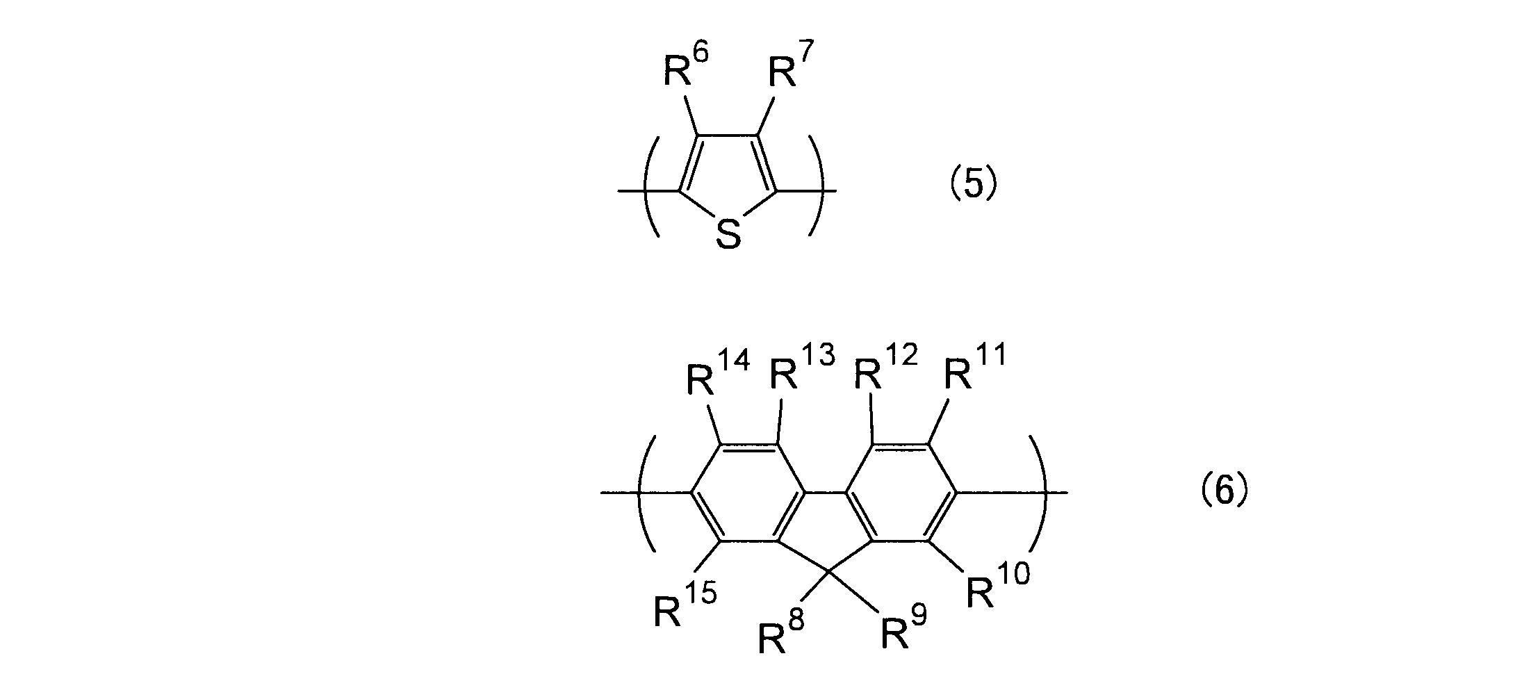
R6~R15で表されるアルキル基は、炭素数が通常1~20であり、直鎖状でも分岐状でもよく、シクロアルキル基でもよい。アルキル基の具体例としては、例えば、メチル基、エチル基、n-プロピル基、i-プロピル基、n-ブチル基、i-ブチル基、tert-ブチル基、sec-ブチル基、3-メチルブチル基、n-ペンチル基、n-ヘキシル基、2-エチルヘキシル基、n-ヘプチル基、n-オクチル基、n-ノニル基、n-デシル基、n-ラウリル基が挙げられる。前記アルキル基中の水素原子はハロゲン原子で置換されていてもよく、具体的には、モノハロメチル基、ジハロメチル基、トリハロメチル基、ペンタハロエチル基等があげられる。ハロゲン原子の中では、フッ素原子で置換されていることが好ましい。フッ素原子で水素原子が置換されたアルキル基の具体例としては、例えば、トリフルオロメチル基、ペンタフルオロエチル基、パーフルオロブチル基、パーフルオロヘキシル基、パーフルオロオクチル基が挙げられる。
R6~R15で表されるアルコキシ基は、炭素数が通常1~20であり、直鎖状でも分岐状でもよく、シクロアルキルオキシ基であってもよい。アルコキシ基の具体例としては、例えば、メトキシ基、エトキシ基、n-プロピルオキシ基、i-プロピルオキシ基、n-ブトキシ基、i-ブトキシ基、sec-ブトキシ基、tert-ブトキシ基、n-ペンチルオキシ基、n-ヘキシルオキシ基、シクロヘキシルオキシ基、n-ヘプチルオキシ基、n-オクチルオキシ基、2-エチルヘキシルオキシ基、n-ノニルオキシ基、n-デシルオキシ基、3,7-ジメチルオクチルオキシ基、n-ラウリルオキシ基が挙げられる。前記アルコキシ基中の水素原子はハロゲン原子で置換されていてもよい。ハロゲン原子の中では、フッ素原子で置換されていることが好ましい。フッ素原子で水素原子が置換されたアルコキシ基の具体例としては、例えば、トリフルオロメトキシ基、ペンタフルオロエトキシ基、パーフルオロブトキシ基、パーフルオロヘキシルオキシ基、パーフルオロオクチルオキシ基が挙げられる。
R6~R15で表されるアリール基は、炭素数が通常6~60であり、置換基を有していてもよい。アリール基が有している置換基としては、例えば、炭素数1~20の直鎖状、分岐状のアルキル基又は炭素数1~20のシクロアルキル基、炭素数1~20の直鎖状、分岐状のアルキル基又は炭素数1~20のシクロアルキル基をその構造中に含むアルコキシ基が挙げられる。アリール基の具体例としては、例えば、フェニル基、C1~C12アルコキシフェニル基(C1~C12は、炭素数1~12であることを示す。以下も同様である。)、C1~C12アルキルフェニル基、1-ナフチル基、2-ナフチル基が挙げられ、炭素数6~20のアリール基が好ましく、C1~C12アルコキシフェニル基、C1~C12アルキルフェニル基がより好ましい。前記アリール基中の水素原子はハロゲン原子で置換されていてもよい。ハロゲン原子の中では、フッ素原子で置換されていることが好ましい。
式(5)中、電荷輸送性の観点からは、R6及びR7の少なくとも一方が、炭素数1~20のアルキル基であることが好ましく、炭素数4~8のアルキル基であることがより好ましい。
式(6)中、モノマーの合成の行いやすさの観点からは、R10~R15は水素原子であることが好ましい。また、素子寿命の観点からはR8及びR9は炭素数1~20のアルキル基又は炭素数6~20のアリール基であることが好ましく、炭素数5~8のアルキル基又は炭素数6~15のアリール基であることがより好ましい。
前記共役高分子化合物は、膜形成能、溶剤への溶解性の観点から、ポリスチレン換算の重量平均分子量が1×10³~1×10⁷であることが好ましく、1×10³~1×10⁶であることがより好ましい。
本発明の有機EL素子が有する発光層中に含まれる前記共役高分子化合物は、一種類であっても二種類以上であってもよい。
前記共役系高分子化合物は、用いる重合反応に適した官能基を有する単量体を合成した後に、必要に応じて、有機溶媒に溶解し、例えば、アルカリや適当な触媒、配位子を用いた公知のアリールカップリング等の重合方法により重合することができる。
[発光層の形成方法]
発光層は、塗布法によって形成されることが好ましい。塗布法は、製造プロセスを簡略化できる点、生産性が優れている点で好ましい。塗布法としてはキャスティング法、スピンコート法、バーコート法、ブレードコート法、ロールコート法、グラビア印刷、スクリーン印刷、インクジェット法等が挙げられる。前記塗布法を用いて発光層を形成する場合、まず発光体と溶媒とを含有する溶液状態の組成物を塗布液として調製し、この塗布液を前述した所定の塗布法によって所望の層又は電極上に塗布し、さらにこれを乾燥することにより、所期の膜厚の発光層を形成することができる。
発光層は、塗布法によって形成されることが好ましい。塗布法は、製造プロセスを簡略化できる点、生産性が優れている点で好ましい。塗布法としてはキャスティング法、スピンコート法、バーコート法、ブレードコート法、ロールコート法、グラビア印刷、スクリーン印刷、インクジェット法等が挙げられる。前記塗布法を用いて発光層を形成する場合、まず発光体と溶媒とを含有する溶液状態の組成物を塗布液として調製し、この塗布液を前述した所定の塗布法によって所望の層又は電極上に塗布し、さらにこれを乾燥することにより、所期の膜厚の発光層を形成することができる。
[他の有機層]
先に述べた陽極側有機層である正孔注入層や正孔輸送層、陰極側有機層である電子注入層や電子輸送層などの他の有機層の材料は特に制限されず、従来の有機EL素子の有機層に用いられている材料を同様に用いることができる。他の有機層は、塗布法、真空蒸着法、スパッタリング法およびラミネート法などの所定の成膜方法によって形成される。
先に述べた陽極側有機層である正孔注入層や正孔輸送層、陰極側有機層である電子注入層や電子輸送層などの他の有機層の材料は特に制限されず、従来の有機EL素子の有機層に用いられている材料を同様に用いることができる。他の有機層は、塗布法、真空蒸着法、スパッタリング法およびラミネート法などの所定の成膜方法によって形成される。
本発明においては、フラーレン誘導体高分子化合物を含ませる有機層としては、特に限定されないが、後述のように発光層および正孔輸送層が好ましい。したがって、先に発光層の構成材料を詳述したことに続いて、正孔輸送層についても、その構成材料について、以下に詳しく説明する。
[正孔輸送層の構成材料]
正孔輸送層に用いる正孔輸送材料としては、高分子化合物の正孔輸送材料、低分子化合物の正孔輸送材料のどちらも使用可能であるが、本発明では、高分子化合物の正孔輸送材料が好ましい。高分子化合物の正孔輸送材料としては、例えば、アミン残基を有する繰り返し単位を含む高分子化合物が挙げられる。ここでいうアミン残基とは、1価または2価の基であり、アミン化合物の窒素原子に結合する1つの置換基から水素原子を1個取り除いた原子団からなる1価の基、またはアミン化合物の窒素原子に結合する2つの置換基からそれぞれ水素原子を1個取り除いた原子団からなる2価の基を意味する。
正孔輸送層に用いる正孔輸送材料としては、高分子化合物の正孔輸送材料、低分子化合物の正孔輸送材料のどちらも使用可能であるが、本発明では、高分子化合物の正孔輸送材料が好ましい。高分子化合物の正孔輸送材料としては、例えば、アミン残基を有する繰り返し単位を含む高分子化合物が挙げられる。ここでいうアミン残基とは、1価または2価の基であり、アミン化合物の窒素原子に結合する1つの置換基から水素原子を1個取り除いた原子団からなる1価の基、またはアミン化合物の窒素原子に結合する2つの置換基からそれぞれ水素原子を1個取り除いた原子団からなる2価の基を意味する。
上記アミン残基を有する繰り返し単位は、アリーレン基、複素環基、およびアリール基などを、置換基として有していることが好ましく、アリールアミン残基(アリールアミン化合物に由来するアミン残基)を有することが好ましい。
アミン残基を有する繰り返し単位は、下記式(7)で示される繰り返し単位であることが好ましい。

〔式中、Ar1、Ar2、Ar3およびAr4は、それぞれ独立にアリーレン基または2価の複素環基を表す。E1、E2およびE3は、それぞれ独立にアリール基または1価の複素環基を表す。aおよびbは、それぞれ独立に0または1を表す。〕
また、Ar1、Ar2、Ar4、E1、E2で表される基から選ばれる基(好ましくはAr4、E1、E2で表される基から選ばれる基)は、該基と同一の窒素原子に結合するAr1、Ar2、Ar3、Ar4、E1、E2およびE3で表される基から選ばれる基と、互いに直結して、又は-O-、-S-、-C(=O)-、-C(=O)-O-、-N(R16)-、-C(=O)-N(R16)-又は-C(R16)(R16)-で結合して、5~7員環を形成していてもよい。例えば、Ar1と同一の窒素原子に結合する基としては、Ar2(a=1の場合)、Ar3(a=0の場合)、Ar4(b=1の場合)、E3(b=0の場合)が挙げられる。R16は、水素原子、アルキル基、アリール基、又は1価の芳香族複素環基を表す。またR16で表される基は、アルキル基、アルコキシ基、アルキルチオ基、置換カルボニル基、置換カルボキシル基、アリール基、アリールオキシ基、アリールチオ基、アラルキル基、1価の芳香族複素環基、フッ素原子又はシアノ基で置換されていてもよい。複数あるR16は互いに同一でも異なっていてもよい。
aおよびbは、0≦a+b≦1であることが好ましい。aおよびbがこの範囲にあると、素子寿命が長くなる傾向がある。
上記アリーレン基は置換基を有していてもよい。置換基としては、アルキル基、アルコキシ基、アルキルチオ基、アリール基、アリールオキシ基、アリールチオ基、アリールアルキル基、アリールアルコキシ基、アリールアルキルチオ基、アリールアルケニル基、アリールアルキニル基、アミノ基、置換アミノ基、シリル基、置換シリル基、シリルオキシ基、置換シリルオキシ基、ハロゲン原子、アシル基、アシルオキシ基、イミン残基、アミド基、酸イミド基、1価の複素環基、カルボキシル基、置換カルボキシル基、シアノ基、および重合可能な置換基等が挙げられ、これらのなかでもアルキル基、アルコキシ基、アルキルチオ基、アリール基、アリールオキシ基、アリールチオ基、置換アミノ基、置換シリル基、置換シリルオキシ基、および1価の複素環基が好ましい。
本発明において2価の複素環基とは、複素環化合物から水素原子2個を除いた残りの原子団をいい、該基は置換基を有していてもよい。置換基としては、アルキル基、アルコキシ基、アルキルチオ基、アリール基、アリールオキシ基、アリールチオ基、アリールアルキル基、アリールアルコキシ基、アリールアルキルチオ基、アリールアルケニル基、アリールアルキニル基、アミノ基、置換アミノ基、シリル基、置換シリル基、シリルオキシ基、置換シリルオキシ基、ハロゲン原子、アシル基、アシルオキシ基、イミン残基、アミド基、酸イミド基、1価の複素環基、カルボキシル基、置換カルボキシル基、シアノ基、重合可能な置換基等が挙げられ、これらのなかでもアルキル基、アルコキシ基、アルキルチオ基、アリール基、アリールオキシ基、アリールチオ基、置換アミノ基、置換シリル基、置換シリルオキシ基、1価の複素環基が好ましい。2価の複素環基における置換基を除いた部分の炭素数は通常3~60程度である。
また置換基を含めた2価の複素環基の全炭素数は、通常3~100程度である。2価の複素環基の中では、2価の芳香族複素環基が好ましい。
上記アリール基は、炭素数が通常6~60程度であり、その具体例としては、フェニル基、C1~C12アルコキシフェニル基(C1~C12は、炭素数1~12であることを示す。以下も同様である。)、C1~C12アルキルフェニル基、1-ナフチル基、2-ナフチル基、1-アントラセニル基、2-アントラセニル基、9-アントラセニル基、ペンタフルオロフェニル基、ベンゾシクロブテン構造を含む基(例えば、下記式(8):

本発明において用いるアミン残基を有する繰り返し単位を含む高分子化合物は、例えば特開2005-251734号公報に記載の方法によって得ることができる。
有機EL素子において、アミン残基を有する繰り返し単位を含む高分子化合物は、熱または光、電子線などの放射線の作用で架橋して溶媒に不溶化していることが好ましい。そのためには重合可能な置換基を有する化合物が重合した高分子化合物であることが好ましい。より具体的には、アミン残基を有する繰り返し単位を含む高分子化合物が、アミン残基を有する繰り返し単位を含み重合可能な置換基を有する高分子化合物が重合してなる高分子化合物であることが好ましい。
重合可能な置換基とは、重合反応を起こすことにより2分子以上の分子間で結合を形成し、化合物を生成可能な置換基のことを表す。このような基としては炭素-炭素多重結合を有する基(たとえば、ビニル基、アセチレン基、ブテニル基、アクリル基、アクリレート基、アクリルアミド基、メタクリル基、メタクリレート基、メタクリルアミド基、アレン基、アリル基、ビニルエーテル基、ビニルアミノ基、フリル基、ピロリル基(ピロール基)、チエニル基(チオフェン基)、シロリル基(シロール基)、ベンゾシクロブテン基構造を含む基等を挙げることができる)、小員環(たとえばシクロプロパン(シクロプロピル基)、シクロプロパン(シクロブチル基)、オキシラン(エポキシ基)、オキセタン(オキセタン基)、ジケテン(ジケテン基)、チイラン(エピスルフィド基)等)を有する基、ラクトン基、ラクタム基、またはシロキサン誘導体を含有する基等がある。また、上記基の他に、エステル結合やアミド結合を形成可能な基の組み合わせなども利用できる。例えばエステル基とアミノ基、エステル基とヒドロキシル基などの組み合わせである。
重合可能な置換基としては下記に示す基が好ましい。

[有機層へのフラーレン誘導体高分子化合物の配合]
本発明において、フラーレン誘導体高分子化合物を含む有機層は、先に説明したいずれの有機層であってもよく、限定されない。しかし、有機EL素子の通常の製造方法では、通常、陽極から陰極に向かって各層を順次に積層していくことと、上記フラーレン誘導体高分子化合物を配合した有機層は塗布法により形成することを考慮すると、塗布法により形成した発光層を上塗りにより損ねないために、陽極側の有機層にフラーレン誘導体高分子化合物を配合することが好ましい。すなわち、発光層及び/又は陽極側有機層(正孔輸送層など)は、本発明における前記フラーレン誘導体高分子化合物を含むことが好ましい。
本発明において、フラーレン誘導体高分子化合物を含む有機層は、先に説明したいずれの有機層であってもよく、限定されない。しかし、有機EL素子の通常の製造方法では、通常、陽極から陰極に向かって各層を順次に積層していくことと、上記フラーレン誘導体高分子化合物を配合した有機層は塗布法により形成することを考慮すると、塗布法により形成した発光層を上塗りにより損ねないために、陽極側の有機層にフラーレン誘導体高分子化合物を配合することが好ましい。すなわち、発光層及び/又は陽極側有機層(正孔輸送層など)は、本発明における前記フラーレン誘導体高分子化合物を含むことが好ましい。
有機層を構成する材料中のフラーレン誘導体高分子化合物の好ましい配合量は、各有機層を構成する材料に依存する部分があるため、全ての有機層に共通の配合量として設定することはできない。以下に有機層が発光層の場合と、正孔輸送層である場合について、フラーレン誘導体高分子化合物の好適な配合量について記載する。
発光層がフラーレン誘導体高分子化合物を含む場合、発光層の重量を100重量部とすると、発光層中のフラーレン誘導体高分子化合物の割合は、0.0001重量部~10重量部が好ましく、0.001重量部~1重量部がより好ましい。
また、正孔輸送層がフラーレン誘導体高分子化合物を含む場合、正孔輸送層の重量を100重量部とすると、正孔輸送層中のフラーレン誘導体高分子化合物の割合は、0.001重量部~100重量部が好ましく、0.01重量部~10重量部がより好ましい。
[有機層を構成する材料へのフラーレン誘導体高分子化合物の配合方法]
有機層を形成するために、通常、先に詳述した高分子化合物が溶媒に溶解された塗布液が用いられる。有機層にフラーレン誘導体高分子化合物を含ませる場合、溶媒に対する有機層構成材料である高分子化合物とフラーレン誘導体高分子化合物の溶解順は特に限定されず、いずれかの高分子化合物を先に溶解させ、続いて他の高分子化合物を溶解させてもよいし、同時に溶解させることも可能である。しかし、好ましくは、有機層を構成する高分子化合物を先に溶解させ、その後、フラーレン誘導体高分子化合物を溶解させる。
有機層を形成するために、通常、先に詳述した高分子化合物が溶媒に溶解された塗布液が用いられる。有機層にフラーレン誘導体高分子化合物を含ませる場合、溶媒に対する有機層構成材料である高分子化合物とフラーレン誘導体高分子化合物の溶解順は特に限定されず、いずれかの高分子化合物を先に溶解させ、続いて他の高分子化合物を溶解させてもよいし、同時に溶解させることも可能である。しかし、好ましくは、有機層を構成する高分子化合物を先に溶解させ、その後、フラーレン誘導体高分子化合物を溶解させる。
[発光装置]
以上説明した有機EL素子は、曲面状や平面状の照明装置、例えばスキャナの光源として用いられる面状光源、および表示装置などの発光装置に好適に用いることができる。
以上説明した有機EL素子は、曲面状や平面状の照明装置、例えばスキャナの光源として用いられる面状光源、および表示装置などの発光装置に好適に用いることができる。
有機EL素子を備える表示装置としては、セグメント表示装置、ドットマトリックス表示装置などを挙げることができる。ドットマトリックス表示装置には、アクティブマトリックス表示装置およびパッシブマトリックス表示装置などがある。有機EL素子は、アクティブマトリックス表示装置、パッシブマトリックス表示装置において、各画素を構成する発光素子として用いられる。また有機EL素子は、セグメント表示装置において、各セグメントを構成する発光素子またはバックライトとして用いられ、液晶表示装置において、バックライトとして用いられる。
以下、本発明をさらに詳細に説明するために実施例を示すが、本発明はこれらに限定されるものではない。
(分子量の測定方法)
以下の実施例において、数平均分子量(Mn)および重量平均分子量(Mw)は、ゲルパーミエーションクロマトグラフィー(GPC)によりポリスチレン換算のものを求めた。具体的には、GPC(東ソー社製、商品名「HLC-8220GPC」)により、TSKgel SuperHM-H(東ソー社製)3本を直列に繋げたカラムを用いて、展開溶媒としてテトラヒドロフランを0.5mL/分の流速で流し、40℃で測定した。検出器には、示差屈折率検出器を用いた。
以下の実施例において、数平均分子量(Mn)および重量平均分子量(Mw)は、ゲルパーミエーションクロマトグラフィー(GPC)によりポリスチレン換算のものを求めた。具体的には、GPC(東ソー社製、商品名「HLC-8220GPC」)により、TSKgel SuperHM-H(東ソー社製)3本を直列に繋げたカラムを用いて、展開溶媒としてテトラヒドロフランを0.5mL/分の流速で流し、40℃で測定した。検出器には、示差屈折率検出器を用いた。
(合成例1) 発光層構成材料(高分子化合物1)の合成
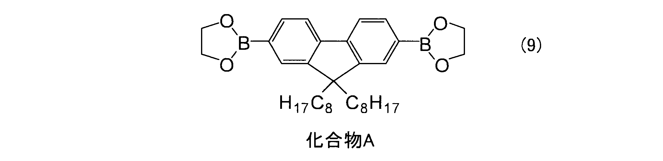
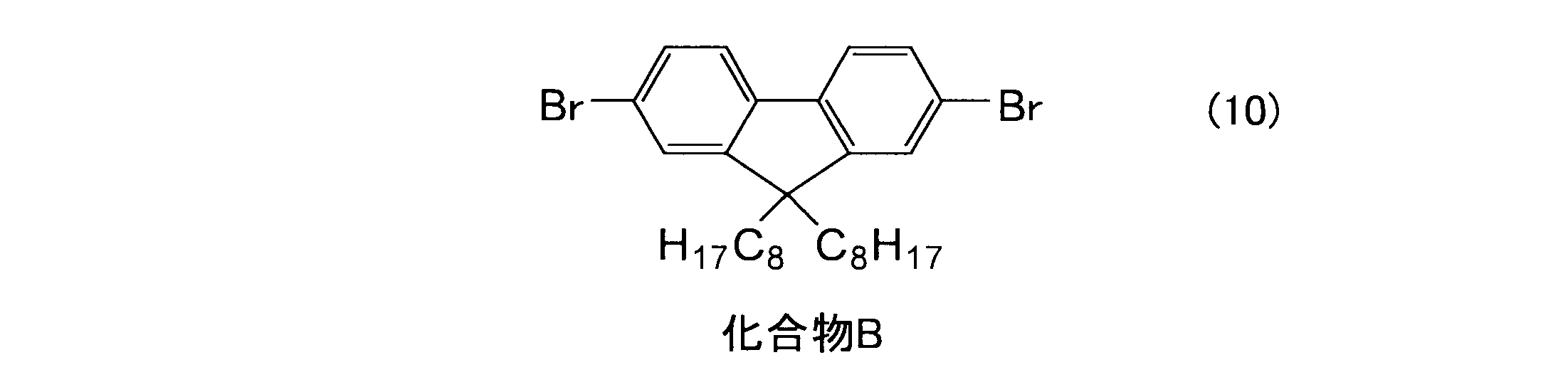
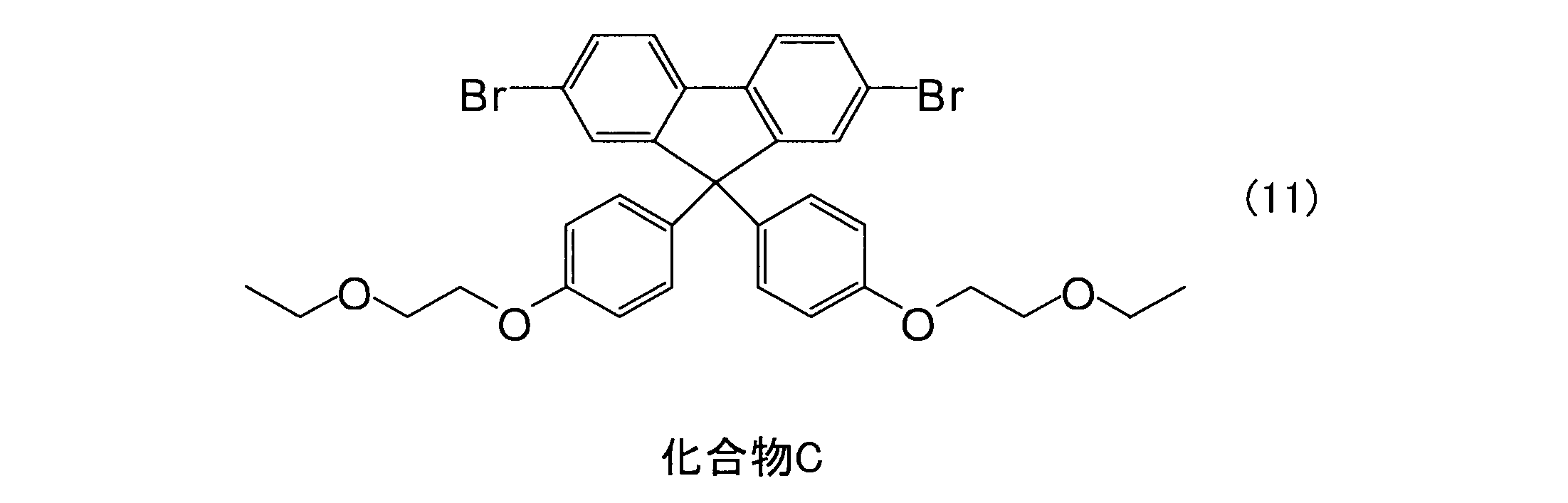
500mLの4口フラスコに、トリスカプリリルメチルアンモニウムクロリド(Triscaprylylmethylammoniumchloride、シグマアルドリッチ社製、商品名「Aliquat336]):1.72g、下記式(9):
500mLの4口フラスコに、トリスカプリリルメチルアンモニウムクロリド(Triscaprylylmethylammoniumchloride、シグマアルドリッチ社製、商品名「Aliquat336]):1.72g、下記式(9):

上記終夜撹拌したフラスコ内容物に10重量%ナトリウムN,N-ジエチルジチオカルバメート水溶液:70mLを加え、さらに還流下で3時間攪拌した。
上記3時間撹拌後に得られた反応液を分液し、有機相を酢酸水溶液及び水で洗浄した後、メタノール中に滴下したところ、沈殿が生じた。得られた沈殿を、ろ過し、減圧乾燥した後、トルエンに溶解させ、シリカゲル-アルミナカラムを通し、トルエンで洗浄した。得られたトルエン溶液をメタノール中に滴下したところ、沈殿が生じた。得られた沈殿を、ろ過し、減圧乾燥した後、トルエンに溶解させ、メタノールに滴下したところ、沈殿が生じた。得られた沈殿を、ろ過し、減圧乾燥して、7.72gの高分子化合物を得た。
得られた高分子化合物は共役系高分子化合物(以下、高分子化合物1と記す場合もある)であり、ポリスチレン換算の数平均分子量Mnは1.2×10⁵であり、ポリスチレン換算の重量平均分子量Mwは2.9×10⁵であった。
(合成例2) 正孔輸送層構成材料(高分子化合物2)の合成
5Lセパラブルフラスコにトリスカプリリルメチルアンモニウムクロリド(Triscaprylylmethylammoniumchloride、シグマアルドリッチ社製、商品名「Aliquat336]):40.18g、前記式(9)で表される化合物A:234.06g、下記式(13):
5Lセパラブルフラスコにトリスカプリリルメチルアンモニウムクロリド(Triscaprylylmethylammoniumchloride、シグマアルドリッチ社製、商品名「Aliquat336]):40.18g、前記式(9)で表される化合物A:234.06g、下記式(13):
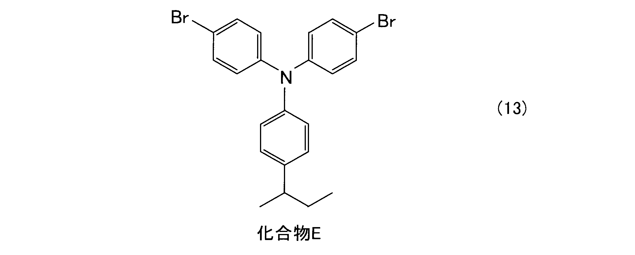
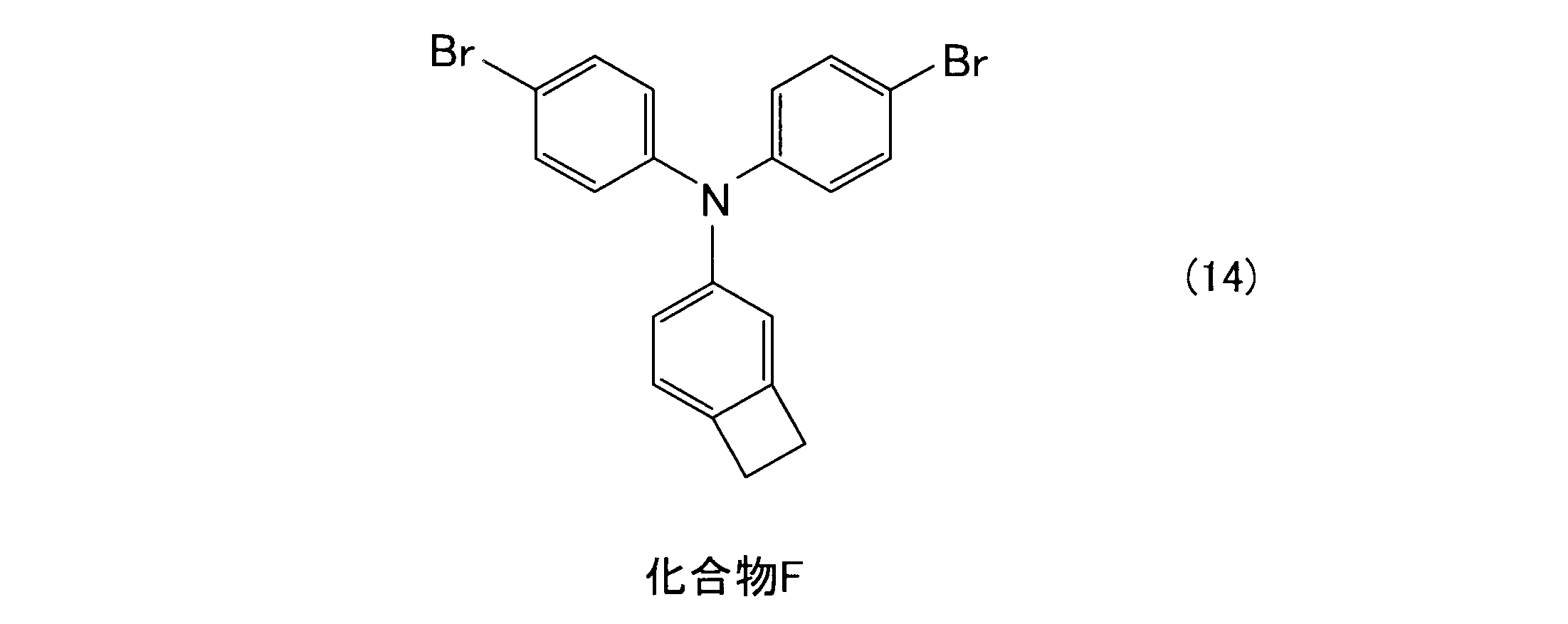
上記30分間バブリングしたフラスコ内容物に、酢酸パラジウム:99.1mg、トリス(o-トリル)ホスフィン:937.0mgを加えた。なお、薬包紙などに付着する酢酸パラジウム、トリス(o-トリル)ホスフィンも158gのトルエンで洗い流すことにより、全てフラスコ内に加え、フラスコ内容物を95℃に加熱した。
上記95℃に加熱したフラスコ内容物に17.5重量%炭酸ナトリウム水溶液:855gを滴下した後、バス温110℃に昇温し、9.5時間攪拌した。その後、フェニルホウ酸:5.39gをトルエン:96mLに溶解して加え、14時間攪拌した。
上記14時間撹拌後のフラスコ内容物に200mLのトルエンを加え、反応液を分液し、有機相を3重量%酢酸水溶液:850mLで2回、更に850mLの水とナトリウムN,N-ジエチルジチオカルバメート:19.89gを加え、4時間攪拌した。分液後、シリカゲル-アルミナカラムを通し、トルエンで洗浄した。得られたトルエン溶液をメタノール50Lに滴下したところ、沈殿が生じた。得られた沈殿を、メタノールで洗浄した。メタノール洗浄後の沈殿を減圧乾燥後、11Lのトルエンに溶解させ、得られたトルエン溶液をメタノール50Lに滴下したところ、沈殿が生じた。得られた沈殿を、ろ過し、減圧乾燥して、278.39gの高分子化合物を得た。
得られた高分子化合物(以下、高分子化合物2と記す場合もある)のポリスチレン換算の数平均分子量Mnは7.7×10⁴であり、ポリスチレン換算の重量平均分子量Mwは3.8×10⁵であった。
(合成例3)フラーレン誘導体高分子化合物F1の合成
以下の合成例では、まず、1,3,5-トリス(オクタデシルオキシ)ベンゼンを合成し、次に、この1,3,5-トリス(オクタデシルオキシ)ベンゼンを用いて、2,4-ジホルミル-1,3,5-トリス(オクタデシルオキシ)ベンゼンを合成した。そして、得られた2,4-ジホルミル-1,3,5-トリス(オクタデシルオキシ)ベンゼンと、フラーレン(C60)と、N-メチルグリシンとを、Prato法により重合させて、目的のフラーレン誘導体高分子化合物F1を得た。
以下の合成例では、まず、1,3,5-トリス(オクタデシルオキシ)ベンゼンを合成し、次に、この1,3,5-トリス(オクタデシルオキシ)ベンゼンを用いて、2,4-ジホルミル-1,3,5-トリス(オクタデシルオキシ)ベンゼンを合成した。そして、得られた2,4-ジホルミル-1,3,5-トリス(オクタデシルオキシ)ベンゼンと、フラーレン(C60)と、N-メチルグリシンとを、Prato法により重合させて、目的のフラーレン誘導体高分子化合物F1を得た。
(1,3,5-トリス(オクタデシルオキシ)ベンゼンの合成)
下記反応式に示すように、フロログルシノール、1-ブロモオクタデカン、炭酸カリウム、DMF等を用いて、1,3,5-トリス(オクタデシルオキシ)ベンゼンを合成した。
下記反応式に示すように、フロログルシノール、1-ブロモオクタデカン、炭酸カリウム、DMF等を用いて、1,3,5-トリス(オクタデシルオキシ)ベンゼンを合成した。

300mLの四ツ口フラスコに、1-ブロモオクタデカン:46.8g(140.2mmol)を入れ、70℃で30分間攪拌した。その後、窒素雰囲気下で脱水DMF:150mL、フロログルシノール:5.75g(45.6mmol)、炭酸カリウム:36.96g(267.4mmol)を加え、70℃で20時間反応させた。反応終了後、溶液を氷水中に注ぎ、析出した固体を濾集した。クロロホルムに溶解させた後、メタノールに再沈殿させた。シリカゲルカラム(クロロホルム/ヘキサン=1:4)、再沈殿(メタノール/アセトン=19:1)により精製した。得られた精製物量は、20.41g(23.10mmol)であった。得られた精製物は、その分析結果を以下に示すように、目的物である(1,3,5-トリス(オクタデシルオキシ)ベンゼン)であった。
収率51%、IR(KBr):2918,2850,1600,1467,1386,1165,1965,908,8156,760,736cm-1、1H NMR(400MHz、CDCl3):d=0.87(t,J=7Hz,9H),1.20-1.42(m,96H),1.67-1.80(m,6H),3.87-3.90(t,J=7Hz,6H),6.05(s,3H)ppm、13C NMR(100MHz,CDCl3):d=14.24,22.80,26.15,29.34,29.48,29.69,29.72,29.80,32.04,68.09,93.79,161.02ppm
(2,4-ジホルミル-1,3,5-トリス(オクタデシルオキシ)ベンゼンの合成)
下記反応式に示すように、1,3,5-トリス(オクタデシルオキシ)ベンゼン、ホスホリルクロリド、DMF等を用いて、2,4-ジホルミル-1,3,5-トリス(オクタデシルオキシ)ベンゼンを合成した。
下記反応式に示すように、1,3,5-トリス(オクタデシルオキシ)ベンゼン、ホスホリルクロリド、DMF等を用いて、2,4-ジホルミル-1,3,5-トリス(オクタデシルオキシ)ベンゼンを合成した。

100mLの四ツ口フラスコに、脱水DMF:60mL(774mmol)を入れ、0℃に冷却した。ホスホリルクロリド:40mL(430mL)を加え、さらに0℃で3時間攪拌した。3時間撹拌したフラスコ内容物に、上記1,3,5-トリス(オクタデシルオキシ)ベンゼン:9.14g(10.3mmol)を加えた後、70℃に加熱して14時間反応させた。反応終了後、反応溶液を氷水に注ぎ、1時間攪拌した。クロロホルムで抽出した後、減圧留去により溶媒を除去し、再沈殿(メタノール:アセトン=4:1)精製した。シリカゲルカラム(クロロホルム:ヘキサン=2:3)でさらに精製した。得られた精製物量は、2.31g(2.46mmol)であった。得られた精製物は、その分析結果を以下に示すように、目的物である(2,4-ジホルミル-1,3,5-トリス(オクタデシルオキシ)ベンゼン)であった。
収率24%、IR(KRS-5):2918,2850,2360,1697,1582,1469,1376,1297,1229,1111,813,720cm-1、1H NMR(400MHz、CDCl3):d=0.86(t,J=6Hz,9H),1.24-1.48(m,96H),1.82(m,9H),3.69-3.99(t,J=8Hz,2H),4.05-4.08(t,J=8Hz,4H),6.20(s,1H),10.31(s,2H)ppm、13C NMR(100MHz,CDCl3):d=14.20,22.78,25.86,26.00,28.91,29.40,29.46,29.61,29.68,29.76,29.80,29.93,32.02,69.43,76.82,78.28,91.93,112.80,166.79,166.88,187.24ppm
(フラーレン誘導体高分子化合物の合成)
下記反応式に示すように、C60フラーレン、2,4-ジホルミル-1,3,5-トリス(オクタデシルオキシ)ベンゼン、o-ジクロロベンゼン、N-メチルグリシン等を用いて、Prato法による重合によって、フラーレン誘導体高分子化合物を合成した。
下記反応式に示すように、C60フラーレン、2,4-ジホルミル-1,3,5-トリス(オクタデシルオキシ)ベンゼン、o-ジクロロベンゼン、N-メチルグリシン等を用いて、Prato法による重合によって、フラーレン誘導体高分子化合物を合成した。

20mLのナスフラスコに、脱水o-ジクロロベンゼン:7mL、上記2,4-ジホルミル-1,3,5-トリス(オクタデシルオキシ)ベンゼン:52.1mL(55.5μmol)、N-メチルグリシン:295.3mg(3.3mmol)、およびC60フラーレン:40.1(55.6μmol)を入れ、減圧脱気により窒素置換を行った。125℃で24時間反応させた。反応終了後、メタノールに再沈殿した。クロロホルム可溶な成分を抽出し、溶媒を減圧留去し、高分子化合物(99.6mg)を得た。得られた高分子化合物は、その分析結果を以下に示すように、目的物であるフラーレン誘導体高分子化合物(以下、フラーレン誘導体高分子化合物F1と記す場合もある)であった。
GPC(光散乱):Mn=1,491,000、Mw/Mn=1.05、[h]=0.0427dLg-1、Rg(SAXS):79.3Å、分解温度(5%):323.6℃、IR(KRS-5):2924,2852,2769,1729,1593,1464,1378,1332,1272,1122,1073,1039,768,742cm-1、1H NMR(400MHz、CDCl3):d=0.3-2.0(br m,111H),3.15-5.88(br,12H),5.90-6.80(br,1H)ppm、UV/Vis(CHCl3):λ=243,273,320nm、元素分析:C 86.38,H 7.43,N 1.86
[塗布溶液A1の作製]
高分子化合物1を1.0重量%の濃度でキシレンに溶解させ、その後、該溶液を孔径0.2μmのテフロン(登録商標)フィルターで濾過し、フラーレン誘導体高分子化合物を含まない発光層形成用塗布溶液A1を作製した。
高分子化合物1を1.0重量%の濃度でキシレンに溶解させ、その後、該溶液を孔径0.2μmのテフロン(登録商標)フィルターで濾過し、フラーレン誘導体高分子化合物を含まない発光層形成用塗布溶液A1を作製した。
[塗布溶液B1の作製]
高分子化合物2を0.5重量%の濃度でキシレンに溶解させ、その後、該溶液を孔径0.2μmのテフロン(登録商標)フィルターで濾過し、フラーレン誘導体高分子化合物を含まない正孔輸送層形成用塗布溶液B1を作製した。
高分子化合物2を0.5重量%の濃度でキシレンに溶解させ、その後、該溶液を孔径0.2μmのテフロン(登録商標)フィルターで濾過し、フラーレン誘導体高分子化合物を含まない正孔輸送層形成用塗布溶液B1を作製した。
[塗布溶液A2の作製]
高分子化合物1を1.0重量%の濃度でキシレンに溶解させ、さらに高分子化合物F1を溶解{高分子化合物1:高分子化合物F1=100:0.02(重量比)}させ、その後、該溶液を孔径0.2μmのテフロン(登録商標)フィルターで濾過し、フラーレン誘導体高分子化合物を含む発光層形成用塗布溶液A2を作製した。
高分子化合物1を1.0重量%の濃度でキシレンに溶解させ、さらに高分子化合物F1を溶解{高分子化合物1:高分子化合物F1=100:0.02(重量比)}させ、その後、該溶液を孔径0.2μmのテフロン(登録商標)フィルターで濾過し、フラーレン誘導体高分子化合物を含む発光層形成用塗布溶液A2を作製した。
[塗布溶液B2の作製]
高分子化合物2を0.5重量%の濃度でキシレンに溶解させ、さらに高分子化合物F1を溶解{高分子化合物2:高分子化合物F1=100:1(重量比)}させ、その後、該溶液を孔径0.2μmのテフロン(登録商標)フィルターで濾過し、フラーレン誘導体高分子化合物を含む正孔輸送層形成用塗布溶液B2を作製した。
高分子化合物2を0.5重量%の濃度でキシレンに溶解させ、さらに高分子化合物F1を溶解{高分子化合物2:高分子化合物F1=100:1(重量比)}させ、その後、該溶液を孔径0.2μmのテフロン(登録商標)フィルターで濾過し、フラーレン誘導体高分子化合物を含む正孔輸送層形成用塗布溶液B2を作製した。
(実施例1)
(発光層にフラーレン誘導体高分子化合物を含む有機EL素子の作製、評価)
スパッタ法により陽極としてのITO膜(膜厚:150nm)が表面に形成されたガラス基板上に、正孔注入層形成用溶液(Plextronics社製、商品名:HIL764)をスピンコートし、さらにこれを大気中ホットプレート上で170℃で15分間乾燥することにより正孔注入層(膜厚:50nm)を形成した。次に、フラーレン誘導体高分子化合物を含まない正孔輸送層形成用塗布溶液B1を正孔注入層上にスピンコートし、グローブボックス中において窒素雰囲気下で、180℃で60分間ベークすることにより正孔輸送層(膜厚:20nm)を形成した。さらに前記フラーレン誘導体高分子化合物を含む発光層形成用塗布溶液A2を上記正孔輸送層上にスピンコートし、発光層を形成した。発光層の形成ではその膜厚が70nmとなるように調整した。
(発光層にフラーレン誘導体高分子化合物を含む有機EL素子の作製、評価)
スパッタ法により陽極としてのITO膜(膜厚:150nm)が表面に形成されたガラス基板上に、正孔注入層形成用溶液(Plextronics社製、商品名:HIL764)をスピンコートし、さらにこれを大気中ホットプレート上で170℃で15分間乾燥することにより正孔注入層(膜厚:50nm)を形成した。次に、フラーレン誘導体高分子化合物を含まない正孔輸送層形成用塗布溶液B1を正孔注入層上にスピンコートし、グローブボックス中において窒素雰囲気下で、180℃で60分間ベークすることにより正孔輸送層(膜厚:20nm)を形成した。さらに前記フラーレン誘導体高分子化合物を含む発光層形成用塗布溶液A2を上記正孔輸送層上にスピンコートし、発光層を形成した。発光層の形成ではその膜厚が70nmとなるように調整した。
その後、窒素雰囲気下で130℃のホットプレートで10分間ベークし、さらにNaFを4nmの厚さで蒸着し、次いで、Alを100nmの厚さで蒸着し、陰極を形成した。蒸着のときの真空度は、1×10⁻⁴Pa~9×10⁻³Paの範囲であった。
素子の形状は、2mm×2mmの正四角形であった。得られた素子を初期輝度5000cd/m2で定電流駆動し、寿命試験をおこなった。初期輝度が4000cd/m2(初期輝度の80%)に低下するまでの時間(これをLT80と呼ぶ)を測定した。測定結果を下記(表1)に示した。
(実施例2)
(正孔輸送層にフラーレン誘導体高分子化合物を含む有機EL素子の作製、評価)
フラーレン誘導体高分子化合物を含まない正孔輸送層形成用塗布溶液B1の代わりにフラーレン誘導体高分子化合物を含む正孔輸送層形成用塗布溶液B2を用い、フラーレン誘導体高分子化合物を含む発光層形成用塗布溶液A2の代わりにフラーレン誘導体高分子化合物を含まない発光層形成用塗布溶液A1を用いたこと以外は、実施例1と同様の方法で有機EL素子を作製し、有機EL素子のLT80を測定した。測定結果を下記(表1)に示した。
(正孔輸送層にフラーレン誘導体高分子化合物を含む有機EL素子の作製、評価)
フラーレン誘導体高分子化合物を含まない正孔輸送層形成用塗布溶液B1の代わりにフラーレン誘導体高分子化合物を含む正孔輸送層形成用塗布溶液B2を用い、フラーレン誘導体高分子化合物を含む発光層形成用塗布溶液A2の代わりにフラーレン誘導体高分子化合物を含まない発光層形成用塗布溶液A1を用いたこと以外は、実施例1と同様の方法で有機EL素子を作製し、有機EL素子のLT80を測定した。測定結果を下記(表1)に示した。
(実施例3)
(発光層及び正孔輸送層の両方にフラーレン誘導体高分子化合物を含む有機EL素子の作製、評価)
フラーレン誘導体高分子化合物を含まない正孔輸送層形成用塗布溶液B1の代わりにフラーレン誘導体高分子化合物を含む正孔輸送層形成用塗布溶液B2を用いたこと以外は、実施例1と同様の方法で有機EL素子を作製し、有機EL素子のLT80を測定した。測定結果を下記(表1)に示した。
(発光層及び正孔輸送層の両方にフラーレン誘導体高分子化合物を含む有機EL素子の作製、評価)
フラーレン誘導体高分子化合物を含まない正孔輸送層形成用塗布溶液B1の代わりにフラーレン誘導体高分子化合物を含む正孔輸送層形成用塗布溶液B2を用いたこと以外は、実施例1と同様の方法で有機EL素子を作製し、有機EL素子のLT80を測定した。測定結果を下記(表1)に示した。
(比較例1)
(いずれの有機層にもフラーレン誘導体高分子化合物を含まない有機EL素子の作製、評価)
フラーレン誘導体高分子化合物を含む発光層形成用塗布溶液A2の代わりにフラーレン誘導体高分子化合物を含まない発光層形成用塗布溶液A1を用いたこと以外は、実施例1と同様の方法で有機EL素子を作製し、有機EL素子のLT80を測定した。測定結果を下記(表1)に示した。
(いずれの有機層にもフラーレン誘導体高分子化合物を含まない有機EL素子の作製、評価)
フラーレン誘導体高分子化合物を含む発光層形成用塗布溶液A2の代わりにフラーレン誘導体高分子化合物を含まない発光層形成用塗布溶液A1を用いたこと以外は、実施例1と同様の方法で有機EL素子を作製し、有機EL素子のLT80を測定した。測定結果を下記(表1)に示した。

(表1)から分かるように、高分子化合物F1を含有する発光層及び/又は正孔輸送層を備える有機EL素子は、高分子化合物F1を含まない有機EL素子に比べて、初期輝度を同じにした場合のLT80寿命が向上した。
Claims (6)
- 陽極、陰極、及び、前記電極間に設けられ、フラーレン誘導体高分子化合物を含む有機層とを備える有機エレクトロルミネッセンス素子であって、
前記フラーレン誘導体高分子化合物は、下記式(1):

下記式(2):

前記フラーレン誘導体高分子化合物は、前記各フラーレン誘導体が該誘導体の構造(X)に結合した前記2価の基(Y)を介して他のフラーレン誘導体と結合している架橋構造を有する、有機エレクトロルミネッセンス素子。 - 発光層を備え、該発光層が前記フラーレン誘導体高分子化合物を含む有機層である請求項1に記載の有機エレクトロルミネッセンス素子。
- 発光層と、該発光層と前記陽極との間に設けられる陽極側有機層を備え、前記陽極側有機層が前記フラーレン誘導体高分子化合物を含む有機層である請求項1に記載の有機エレクトロルミネッセンス素子。
- 発光層と、該発光層と前記陽極との間に設けられる陽極側有機層を備え、前記発光層と前記陽極側有機層とが前記フラーレン誘導体高分子化合物を含む有機層である請求項1に記載の有機エレクトロルミネッセンス素子。
- 前記陽極側有機層が正孔輸送層である、請求項3または4に記載の有機エレクトロルミネッセンス素子。
- 請求項1に記載の有機エレクトロルミネッセンス素子を備える発光装置。
Applications Claiming Priority (2)
| Application Number | Priority Date | Filing Date | Title |
|---|---|---|---|
| JP2010-238588 | 2010-10-25 | ||
| JP2010238588A JP2012094583A (ja) | 2010-10-25 | 2010-10-25 | 有機エレクトロルミネッセンス素子および発光装置 |
Publications (1)
| Publication Number | Publication Date |
|---|---|
| WO2012056904A1 true WO2012056904A1 (ja) | 2012-05-03 |
Family
ID=45993629
Family Applications (1)
| Application Number | Title | Priority Date | Filing Date |
|---|---|---|---|
| PCT/JP2011/073673 Ceased WO2012056904A1 (ja) | 2010-10-25 | 2011-10-14 | 有機エレクトロルミネッセンス素子および発光装置 |
Country Status (3)
| Country | Link |
|---|---|
| JP (1) | JP2012094583A (ja) |
| TW (1) | TW201229200A (ja) |
| WO (1) | WO2012056904A1 (ja) |
Cited By (2)
| Publication number | Priority date | Publication date | Assignee | Title |
|---|---|---|---|---|
| EP3173435A1 (en) | 2015-11-26 | 2017-05-31 | Merck Patent GmbH | Semiconducting mixtures |
| CN108976249A (zh) * | 2017-12-29 | 2018-12-11 | 南京林业大学 | 一种三聚茚咔咯-富勒烯的星型化合物的制备方法 |
Families Citing this family (1)
| Publication number | Priority date | Publication date | Assignee | Title |
|---|---|---|---|---|
| JP5955660B2 (ja) * | 2012-06-20 | 2016-07-20 | 住友化学株式会社 | 組成物、高分子化合物およびそれらを用いた発光素子 |
Citations (2)
| Publication number | Priority date | Publication date | Assignee | Title |
|---|---|---|---|---|
| WO2010150792A1 (ja) * | 2009-06-23 | 2010-12-29 | 住友化学株式会社 | 有機エレクトロルミネッセンス素子 |
| JP2011126993A (ja) * | 2009-12-17 | 2011-06-30 | Tokyo Institute Of Technology | フラーレン高分子およびその製造方法 |
-
2010
- 2010-10-25 JP JP2010238588A patent/JP2012094583A/ja not_active Withdrawn
-
2011
- 2011-10-14 WO PCT/JP2011/073673 patent/WO2012056904A1/ja not_active Ceased
- 2011-10-21 TW TW100138234A patent/TW201229200A/zh unknown
Patent Citations (3)
| Publication number | Priority date | Publication date | Assignee | Title |
|---|---|---|---|---|
| WO2010150792A1 (ja) * | 2009-06-23 | 2010-12-29 | 住友化学株式会社 | 有機エレクトロルミネッセンス素子 |
| JP2011187908A (ja) * | 2009-06-23 | 2011-09-22 | Sumitomo Chemical Co Ltd | 有機エレクトロルミネッセンス素子 |
| JP2011126993A (ja) * | 2009-12-17 | 2011-06-30 | Tokyo Institute Of Technology | フラーレン高分子およびその製造方法 |
Non-Patent Citations (2)
| Title |
|---|
| MAURIZIO PRATO ET AL.: "Fulleropyrrolidines: A Family of Full-Fledged Fullerene Derivatives", ACCOUNTS OF CHEMICAL RESEARCH, vol. 31, no. 9, 21 June 2000 (2000-06-21), pages 519 - 526 * |
| ROGER C. HIORNS ET AL.: "Alternatively Linking fullerene and Conjugated Polymers", JOURNAL OF POLYMER SCIENCE PART A: POLYMER CHEMISTRY, vol. 47, no. ISSUE, 25 March 2009 (2009-03-25), pages 2304 - 2317 * |
Cited By (3)
| Publication number | Priority date | Publication date | Assignee | Title |
|---|---|---|---|---|
| EP3173435A1 (en) | 2015-11-26 | 2017-05-31 | Merck Patent GmbH | Semiconducting mixtures |
| WO2017088955A1 (en) | 2015-11-26 | 2017-06-01 | Merck Patent Gmbh | Semiconducting mixtures |
| CN108976249A (zh) * | 2017-12-29 | 2018-12-11 | 南京林业大学 | 一种三聚茚咔咯-富勒烯的星型化合物的制备方法 |
Also Published As
| Publication number | Publication date |
|---|---|
| TW201229200A (en) | 2012-07-16 |
| JP2012094583A (ja) | 2012-05-17 |
Similar Documents
| Publication | Publication Date | Title |
|---|---|---|
| TW201035162A (en) | Polymeric (high molecular) compound and light emitting element using such polymeric compound | |
| WO2008136492A1 (ja) | ピレン系高分子化合物及びそれを用いてなる発光素子 | |
| TWI479007B (zh) | 發光材料、印墨組成物、薄膜、發光元件及發光元件之製造方法 | |
| WO2010150792A1 (ja) | 有機エレクトロルミネッセンス素子 | |
| KR20190055184A (ko) | 발광 소자 | |
| JP6923691B2 (ja) | 発光素子 | |
| JP2020009770A (ja) | 発光素子 | |
| WO2012056904A1 (ja) | 有機エレクトロルミネッセンス素子および発光装置 | |
| JP6595070B1 (ja) | 発光素子 | |
| KR102120300B1 (ko) | 발광 소자 | |
| WO2012011412A1 (ja) | 有機エレクトロルミネッセンス素子 | |
| JP5834385B2 (ja) | 有機エレクトロルミネッセンス素子および高分子発光体組成物 | |
| JP6923692B2 (ja) | 発光素子の製造方法 | |
| Lengvinaite et al. | Polyethers containing 2-phenylindol-1-yl moieties as host materials for light emitting diodes | |
| JP5799506B2 (ja) | 有機エレクトロルミネッセンス素子および高分子発光体組成物 | |
| WO2022065101A1 (ja) | 発光素子及び組成物 | |
| JP7058792B2 (ja) | 発光素子及び組成物 | |
| KR100881814B1 (ko) | 고색순도 청색 전계발광 공중합체 및 이를 이용한 유기전계발광 소자 | |
| WO2017221822A1 (ja) | 発光素子 | |
| JP2026053955A (ja) | 発光素子 | |
| JP2026053954A (ja) | 発光素子 | |
| KR100796032B1 (ko) | 청색 전계발광 고분자 및 이를 이용한 유기 전계발광 소자 | |
| JP2021080401A (ja) | 高分子化合物を含む組成物、該高分子化合物の製造方法及び該高分子化合物を用いてなる発光素子の製造方法 | |
| KR20080078494A (ko) | 고효율 청색 전계발광 공중합체 및 이를 이용한 유기전계발광 소자 | |
| WO2017170325A1 (ja) | 発光素子 |
Legal Events
| Date | Code | Title | Description |
|---|---|---|---|
| 121 | Ep: the epo has been informed by wipo that ep was designated in this application |
Ref document number: 11836043 Country of ref document: EP Kind code of ref document: A1 |
|
| NENP | Non-entry into the national phase |
Ref country code: DE |
|
| 122 | Ep: pct application non-entry in european phase |
Ref document number: 11836043 Country of ref document: EP Kind code of ref document: A1 |