WO2012056659A1 - アクティブマトリクス基板及びその製造方法、対向基板及びその製造方法、並びに表示パネル - Google Patents
アクティブマトリクス基板及びその製造方法、対向基板及びその製造方法、並びに表示パネル Download PDFInfo
- Publication number
- WO2012056659A1 WO2012056659A1 PCT/JP2011/005888 JP2011005888W WO2012056659A1 WO 2012056659 A1 WO2012056659 A1 WO 2012056659A1 JP 2011005888 W JP2011005888 W JP 2011005888W WO 2012056659 A1 WO2012056659 A1 WO 2012056659A1
- Authority
- WO
- WIPO (PCT)
- Prior art keywords
- transparent
- conductive layer
- transparent conductive
- subpixel
- film
- Prior art date
- Legal status (The legal status is an assumption and is not a legal conclusion. Google has not performed a legal analysis and makes no representation as to the accuracy of the status listed.)
- Ceased
Links
Images







Classifications
-
- G—PHYSICS
- G02—OPTICS
- G02F—OPTICAL DEVICES OR ARRANGEMENTS FOR THE CONTROL OF LIGHT BY MODIFICATION OF THE OPTICAL PROPERTIES OF THE MEDIA OF THE ELEMENTS INVOLVED THEREIN; NON-LINEAR OPTICS; FREQUENCY-CHANGING OF LIGHT; OPTICAL LOGIC ELEMENTS; OPTICAL ANALOGUE/DIGITAL CONVERTERS
- G02F1/00—Devices or arrangements for the control of the intensity, colour, phase, polarisation or direction of light arriving from an independent light source, e.g. switching, gating or modulating; Non-linear optics
- G02F1/01—Devices or arrangements for the control of the intensity, colour, phase, polarisation or direction of light arriving from an independent light source, e.g. switching, gating or modulating; Non-linear optics for the control of the intensity, phase, polarisation or colour
- G02F1/13—Devices or arrangements for the control of the intensity, colour, phase, polarisation or direction of light arriving from an independent light source, e.g. switching, gating or modulating; Non-linear optics for the control of the intensity, phase, polarisation or colour based on liquid crystals, e.g. single liquid crystal display cells
- G02F1/133—Constructional arrangements; Operation of liquid crystal cells; Circuit arrangements
- G02F1/1333—Constructional arrangements; Manufacturing methods
- G02F1/1343—Electrodes
- G02F1/13439—Electrodes characterised by their electrical, optical, physical properties; materials therefor; method of making
Definitions
- the present invention relates to an active matrix substrate, a manufacturing method thereof, a counter substrate, a manufacturing method thereof, and a display panel, and more particularly to a configuration of a pixel electrode in an active matrix substrate and a common electrode in a counter substrate and a method of forming the same.
- the liquid crystal display panel is, for example, an active matrix substrate provided with a thin film transistor (hereinafter also referred to as “TFT”) or a pixel electrode for each sub-pixel which is a minimum unit of an image, and an active matrix substrate. And a counter substrate provided with a common electrode and the like, and an active matrix substrate and a liquid crystal layer sealed between the counter substrate.
- TFT thin film transistor
- a counter substrate provided with a common electrode and the like, and an active matrix substrate and a liquid crystal layer sealed between the counter substrate.
- the counter substrate includes, for example, a black matrix provided in a lattice form on a glass substrate, and a plurality of black matrixes, that is, a red layer, a green layer, a blue layer, and the like provided for each subpixel. And a common electrode provided so as to cover the black matrix and each colored layer.
- the common electrode is formed of a transparent conductive film formed by a sputtering method, and thus, for example, a red pixel-provided subpixel for performing gray scale display and a green layer are provided.
- the film thicknesses of the common electrodes in the sub-pixel that performs green gradation display and the sub-pixel that performs blue gradation display provided with the blue layer are the same in the substrate plane, and each sub-pixel has a desired thickness. It is difficult to obtain optical characteristics.
- each pixel electrode is formed by patterning a transparent conductive film formed by sputtering, so that, for example, a sub-pixel that performs red gradation display, a green gradation,
- the film thickness of each pixel electrode in the sub-pixel that performs display and the sub-pixel that performs blue gradation display is the same in the substrate surface, and it is difficult to obtain desired optical characteristics for each sub-pixel.
- obtaining desired optical characteristics for each display color sub-pixel in each pixel electrode and common electrode is effective in improving the transmittance of an active matrix substrate or a counter substrate and a display panel including them.
- Patent Document 1 after applying ink in which fine particles of a transparent conductive film material are dispersed in a binder by inkjet, the coating film is baked to form a transparent conductive film with the amount of ink applied to form the transparent conductive film.
- Display device having a color filter in which the optical film thickness of the transparent conductive film is made different for each color of each pixel (subpixel) by controlling the film thickness of each pixel (subpixel) and its manufacture A method is disclosed.
- the thickness of the transparent conductive film can be set for each colored layer, and desired optical characteristics can be obtained for each colored layer. It is necessary to introduce an ink jet equipment for forming an existing manufacturing line.
- a sputtering device and an etching device are provided for each type of transparent conductive film such as ITO (Indium Tin Oxide) or IZO (Indium Zinc Oxide).
- ITO Indium Tin Oxide
- IZO Indium Zinc Oxide
- the present invention has been made in view of such points, and an object of the present invention is to obtain desired optical characteristics for each sub-pixel while suppressing a decrease in manufacturing efficiency.
- the first transparent first conductive layer formed by the first transparent conductive film and the second transparent first conductive film formed by the second transparent conductive film A first transparent second conductive layer, and a second transparent conductive film, each having a third transparent conductive layer formed of the first transparent conductive film in the second subpixel.
- the second transparent second conductive layer is formed by the above-described method, and the third sub-pixel has the first transparent third conductive layer formed by the first transparent conductive film.
- an active matrix substrate includes a plurality of pixel electrodes provided in a matrix on the substrate, and a first sub-pixel and a first sub-pixel for displaying different colors corresponding to each pixel electrode.
- the pixel electrode of the first subpixel includes the first transparent first conductive layer formed of the first transparent conductive film, the second transparent first conductive layer formed of the second transparent conductive film, And a third transparent conductive layer formed by the third transparent conductive film, and a pixel electrode of the second subpixel is formed by the first transparent conductive film, the first transparent second conductive layer, and the second transparent conductive layer. Since the pixel electrode of the third subpixel has the first transparent third conductive layer formed by the first transparent conductive film, the second transparent second conductive layer formed by the film has each second subpixel. The film thickness of the pixel electrode in the pixel decreases in the order of the first subpixel, the second subpixel, and the third subpixel.
- each pixel electrode is formed by appropriately selecting three types of transparent conductive films, ie, a first transparent conductive film, a second transparent conductive film, and a third transparent conductive film. , Three types of dedicated sputtering apparatuses for forming the second transparent conductive film and the third transparent conductive film, respectively, and for etching the first transparent conductive film, the second transparent conductive film, and the third transparent conductive film, respectively.
- the concentration of processing in the specific sputtering apparatus and the corresponding etching apparatus is suppressed, and the decrease in the manufacturing efficiency of the active matrix substrate is suppressed. Therefore, in the active matrix substrate, it is possible to obtain a desired optical characteristic for each sub-pixel while suppressing a decrease in manufacturing efficiency.
- the first transparent first conductive layer, the second transparent first conductive layer, and the third transparent conductive layer may be laminated in order.
- the first transparent first conductive layer, the second transparent first conductive layer, and the third transparent conductive layer are sequentially laminated.
- the first transparent conductive film is patterned to form the first transparent first conductive layer, the first transparent second conductive layer, and the first transparent third conductive layer, respectively.
- the second transparent conductive film is patterned to form a second transparent first conductive layer and a second transparent second conductive layer, respectively, and further, a third transparent conductive film is formed.
- the third transparent conductive film is patterned to form a third transparent conductive layer, whereby an active matrix substrate is specifically manufactured.
- the first transparent conductive film is a polycrystalline indium tin oxide film
- the second transparent conductive film is formed by annealing an amorphous indium tin oxide film
- the third transparent conductive film is An indium zinc oxide film may be used.
- the first transparent conductive film is a polycrystalline indium tin oxide film
- the second transparent conductive film is formed by annealing an amorphous indium tin oxide film
- the third transparent conductive film Is an indium zinc oxide film, for example, if the second transparent conductive film is annealed after being patterned, when the second transparent conductive film is patterned by etching, the first transparent conductive film (polycrystalline Since the indium tin oxide film) has higher etching resistance than the second transparent conductive film (amorphous indium tin oxide film), the etching of the first transparent conductive film is difficult to proceed, and the third transparent conductive film
- the first transparent conductive film polycrystalline indium tin oxide film
- the second transparent conductive film amorphous indium tin oxide film
- the active matrix substrate manufacturing method includes a plurality of pixel electrodes provided in a matrix on the substrate, and a first sub-pixel for displaying different colors corresponding to the pixel electrodes.
- the first transparent first conductive layer and the second transparent conductive layer are formed in which the pixel electrode of the first subpixel is formed by patterning the first transparent conductive film in the first transparent conductive layer forming step.
- the pixel electrode of the second subpixel is formed by patterning the first transparent conductive film in the first transparent conductive layer forming step, and the second transparent conductive layer forming step is the second in the second transparent conductive layer forming step.
- a second transparent second conductive layer formed by patterning the transparent conductive film, and the pixel electrode of the third subpixel was formed by patterning the first transparent conductive film in the first transparent conductive layer forming step Since it has the first transparent third conductive layer, the image in each sub-pixel The thickness of the electrode, the first sub-pixel, becomes thinner in the order of the second sub-pixel and the third sub-pixels. For this reason, the pixel electrode of the first subpixel, the pixel electrode of the second subpixel, and the pixel electrode of the third subpixel have different film thicknesses. Characteristics are obtained.
- each pixel electrode is formed by appropriately selecting three types of transparent conductive films, ie, a first transparent conductive film, a second transparent conductive film, and a third transparent conductive film.
- Three types of dedicated sputtering apparatuses for forming the second transparent conductive film and the third transparent conductive film, respectively, and for etching the first transparent conductive film, the second transparent conductive film, and the third transparent conductive film, respectively.
- the concentration of processing in the specific sputtering apparatus and the corresponding etching apparatus is suppressed, and the decrease in the manufacturing efficiency of the active matrix substrate is suppressed. Therefore, in the active matrix substrate, it is possible to obtain a desired optical characteristic for each sub-pixel while suppressing a decrease in manufacturing efficiency.
- the first transparent conductive layer forming step, the second transparent conductive layer forming step, and the third transparent conductive layer forming step are sequentially performed, and the first transparent conductive film is a polycrystalline indium tin oxide film, and the second transparent conductive layer is formed.
- the conductive film is formed as an amorphous indium tin oxide film in the second transparent conductive layer forming step, and after patterning the formed indium tin oxide film, it is polycrystallized by annealing treatment,
- the third transparent conductive film may be an indium zinc oxide film.
- a 1st transparent conductive layer formation process, a 2nd transparent conductive layer formation process, and a 3rd transparent conductive layer formation process are performed in order, and the 1st transparent conductive film is a polycrystalline indium tin oxide film
- the second transparent conductive film is formed as an amorphous indium tin oxide film, patterned and then polycrystallized by annealing, and the third transparent conductive film is an indium zinc oxide film.
- the first transparent conductive film polycrystalline indium tin oxide film
- the second transparent conductive film is more resistant than the second transparent conductive film (amorphous indium tin oxide film).
- the etching of the first transparent conductive film (first transparent third conductive layer) becomes difficult to proceed, and the third transparent conductive film is etched in the third transparent conductive layer forming step.
- the first transparent conductive film (polycrystalline indium tin oxide film) and the second transparent conductive film has higher etching resistance than the third transparent conductive film (indium zinc oxide film), so that the first transparent conductive film (first transparent third conductive layer) and the second transparent conductive film (second transparent second conductive). Layer) is less likely to progress.
- the counter substrate includes a common electrode provided on the substrate, and the first subpixel, the second subpixel, and the third subpixel for displaying different colors from each other with respect to the common electrode.
- the common electrode is a first transparent first conductive layer formed by a first transparent conductive film and a second transparent conductive film formed by a second transparent conductive film.
- a first transparent second conductive layer formed of the first transparent conductive film in the second subpixel; and a third transparent conductive layer formed of the first conductive layer and the third transparent conductive film;
- First transparent first conductive layer, first transparent second conductive layer, first transparent third conductive layer Second transparent first conductive layer, a second transparent second conductive layer and the third transparent conductive layer is characterized by being connected to each other.
- the common electrode includes, in the first subpixel, the first transparent first conductive layer formed by the first transparent conductive film and the second transparent first conductive layer formed by the second transparent conductive film. And a third transparent conductive layer formed by the third transparent conductive film, and in the second subpixel, by the first transparent second conductive layer and the second transparent conductive film formed by the first transparent conductive film.
- a second transparent second conductive layer formed; the third subpixel includes a first transparent third conductive layer formed of the first transparent conductive film; the first transparent first conductive layer; Since the transparent second conductive layer, the first transparent third conductive layer, the second transparent first conductive layer, the second transparent second conductive layer, and the third transparent conductive layer are connected to each other, the common electrode is specifically configured.
- the thickness of the common electrode in each subpixel is reduced in the order of the first subpixel, the second subpixel, and the third subpixel. It made. Therefore, since the common electrode has different film thicknesses in the first subpixel, the second subpixel, and the third subpixel, desired optical characteristics can be obtained for each subpixel in the counter substrate.
- the common electrode is formed by appropriately selecting three types of transparent conductive films of the first transparent conductive film, the second transparent conductive film, and the third transparent conductive film, for example, the first transparent conductive film, Three types of dedicated sputtering apparatuses for forming the second transparent conductive film and the third transparent conductive film, respectively, and for etching the first transparent conductive film, the second transparent conductive film, and the third transparent conductive film, respectively.
- the concentration of processing in a specific sputtering apparatus and the corresponding etching apparatus is suppressed, and a decrease in the manufacturing efficiency of the counter substrate is suppressed. Therefore, in the counter substrate, it is possible to obtain a desired optical characteristic for each sub-pixel while suppressing a decrease in manufacturing efficiency.
- the first transparent first conductive layer, the first transparent second conductive layer, and the first transparent third conductive layer may be integrally formed.
- the first transparent first conductive layer, the first transparent second conductive layer, and the first transparent third conductive layer are integrally formed, the first transparent first conductive layer and the first transparent The second conductive layer, the first transparent third conductive layer, the second transparent first conductive layer, the second transparent second conductive layer, and the third transparent conductive layer are connected to each other to specifically configure the common electrode.
- the substrate, the first transparent first conductive layer, the first transparent second conductive layer, the first transparent third conductive layer, the second transparent first conductive layer, the second transparent second conductive layer, and the third transparent conductive layer may be provided between the first colored pixel, the second colored pixel, and the third colored pixel, respectively.
- a so-called counter substrate called a color filter substrate is specifically configured.
- the counter substrate manufacturing method includes a common electrode provided on the substrate, and a first subpixel, a second subpixel, and a third subpixel for displaying different colors with respect to the common electrode.
- a second transparent second conductive layer is applied to the sub-pixel.
- a third transparent conductive layer forming step of forming a transparent conductive layer is
- the first transparent first conductive layer and the second transparent conductive layer are formed by patterning the first transparent conductive film in the first sub-pixel in the first transparent conductive layer forming step.
- a second transparent first conductive layer formed by patterning the second transparent conductive film in the forming step, and a third transparent conductive layer formed by patterning the third transparent conductive layer in the third transparent conductive layer forming step.
- a first transparent second conductive layer formed by patterning the first transparent conductive film in the first transparent conductive layer forming step, and a second transparent conductive in the second transparent conductive layer forming step.
- a first transparent third layer formed by patterning the first transparent conductive film in the first transparent conductive layer forming step in the third sub-pixel.
- the common electrode is specifically formed, and the film thickness of the common electrode in each subpixel is the first subpixel, the second subpixel, and the third subpixel. It becomes thinner in the order of pixels. Therefore, since the common electrode has different film thicknesses in the first subpixel, the second subpixel, and the third subpixel, desired optical characteristics can be obtained for each subpixel in the counter substrate.
- the common electrode is formed by appropriately selecting three types of transparent conductive films of the first transparent conductive film, the second transparent conductive film, and the third transparent conductive film, for example, the first transparent conductive film.
- Three types of dedicated sputtering apparatuses for forming the second transparent conductive film and the third transparent conductive film, respectively, and for etching the first transparent conductive film, the second transparent conductive film, and the third transparent conductive film, respectively.
- the concentration of processing in a specific sputtering apparatus and the corresponding etching apparatus is suppressed, and a decrease in the manufacturing efficiency of the counter substrate is suppressed. Therefore, in the counter substrate, it is possible to obtain a desired optical characteristic for each sub-pixel while suppressing a decrease in manufacturing efficiency.
- the display panel according to the present invention is a display panel including an active matrix substrate and a counter substrate provided so as to face each other, and a display medium layer provided between the active matrix substrate and the counter substrate.
- the active matrix substrate includes a plurality of pixel electrodes provided in a matrix on the substrate, and a first subpixel, a second subpixel, and a second subpixel for displaying different colors corresponding to the pixel electrodes, respectively.
- a third subpixel is defined, and the pixel electrode of the first subpixel is a first transparent first conductive layer formed by a first transparent conductive film, and a second transparent first conductive formed by a second transparent conductive film.
- the pixel electrode of the first subpixel is the first transparent first conductive layer formed by the first transparent conductive film and the second transparent film formed by the second transparent conductive film.
- a first transparent second conductive layer having a first conductive layer and a third transparent conductive layer formed by a third transparent conductive film, wherein the pixel electrode of the second subpixel is formed by the first transparent conductive film;
- a second transparent second conductive layer formed by the second transparent conductive film, and the pixel electrode of the third subpixel has the first transparent third conductive layer formed by the first transparent conductive film. Therefore, the film thickness of the pixel electrode in each subpixel becomes thinner in the order of the first subpixel, the second subpixel, and the third subpixel.
- each pixel electrode is formed by appropriately selecting three types of transparent conductive films, ie, a first transparent conductive film, a second transparent conductive film, and a third transparent conductive film. , Three types of dedicated sputtering apparatuses for forming the second transparent conductive film and the third transparent conductive film, respectively, and for etching the first transparent conductive film, the second transparent conductive film, and the third transparent conductive film, respectively.
- the concentration of processing in the specific sputtering apparatus and the corresponding etching apparatus is suppressed, and the decrease in the manufacturing efficiency of the active matrix substrate is suppressed. Therefore, in a display panel including an active matrix substrate, it is possible to obtain a desired optical characteristic for each subpixel while suppressing a decrease in manufacturing efficiency.
- the display panel according to the present invention is a display panel including an active matrix substrate and a counter substrate provided so as to face each other, and a display medium layer provided between the active matrix substrate and the counter substrate.
- the counter substrate includes a common electrode provided on the substrate, and a first subpixel, a second subpixel, and a third subpixel for displaying different colors with respect to the common electrode are defined.
- the common electrode includes a first transparent first conductive layer formed of a first transparent conductive film, a second transparent first conductive layer formed of a second transparent conductive film, and a third transparent in the first subpixel.
- the conductive layer, the first transparent third conductive layer, the second transparent first conductive layer, the second transparent second conductive layer, and the third transparent conductive layer are connected to each other.
- the common electrode provided on the counter substrate includes the first transparent first conductive layer formed by the first transparent conductive film and the second transparent conductive film formed by the first transparent conductive film in the first subpixel.
- the electrode is specifically configured, and the film thickness of the common electrode in each subpixel is such that the first subpixel, the second subpixel, and the subpixel Thinner in the order of the third sub-pixel. Therefore, since the common electrode has different film thicknesses in the first subpixel, the second subpixel, and the third subpixel, desired optical characteristics can be obtained for each subpixel in the counter substrate.
- the common electrode is formed by appropriately selecting three types of transparent conductive films of the first transparent conductive film, the second transparent conductive film, and the third transparent conductive film, for example, the first transparent conductive film.
- Three types of dedicated sputtering apparatuses for forming the second transparent conductive film and the third transparent conductive film, respectively, and for etching the first transparent conductive film, the second transparent conductive film, and the third transparent conductive film, respectively.
- the concentration of processing in a specific sputtering apparatus and the corresponding etching apparatus is suppressed, and a decrease in the manufacturing efficiency of the counter substrate is suppressed. Therefore, in the display panel including the counter substrate, it is possible to obtain a desired optical characteristic for each sub-pixel while suppressing a decrease in manufacturing efficiency.
- the second transparent pixel has a third transparent conductive layer formed of a conductive film, and a second transparent conductive layer formed of the first transparent conductive film and the second transparent conductive film formed of the first transparent conductive film in the second subpixel. Since it has a transparent second conductive layer and the third sub-pixel has the first transparent third conductive layer formed by the first transparent conductive film, each sub-pixel can be prevented from being reduced in manufacturing efficiency. Desired optical characteristics can be obtained for each time.
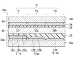
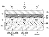
- FIG. 1 is a cross-sectional view of the liquid crystal display panel according to the first embodiment.
- FIG. 2 is a simplified cross-sectional view of the liquid crystal display panel according to the first embodiment.
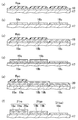
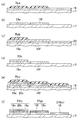
- FIG. 3 is a cross-sectional view illustrating a part of the manufacturing process of the active matrix substrate constituting the liquid crystal display panel according to the first embodiment.
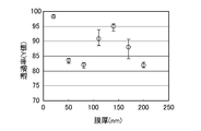
- FIG. 4 is a graph showing the relationship between the film thickness and the transmittance of the transparent conductive film obtained in the experiment according to the first embodiment.
- FIG. 5 is a graph showing the relationship between the film thickness and chromaticity of the transparent conductive film obtained in the experiment according to the first embodiment.
- FIG. 6 is a simplified cross-sectional view of the liquid crystal display panel according to the second embodiment.
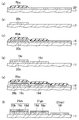
- FIG. 7 is a cross-sectional view illustrating a part of the manufacturing process of the active matrix substrate constituting the liquid crystal display panel according to the second embodiment.
- FIG. 8 is a simplified cross-sectional view of the liquid crystal display panel according to the third embodiment.
- FIG. 9 is a cross-sectional view illustrating a part of the manufacturing process of the active matrix substrate constituting the liquid crystal display panel according to the third embodiment.
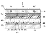
- FIG. 10 is a cross-sectional view of the liquid crystal display panel according to the fourth embodiment.
- FIG. 11 is a simplified cross-sectional view of the liquid crystal display panel according to the fourth embodiment.
- FIG. 12 is a cross-sectional view illustrating a part of the manufacturing process of the counter substrate constituting the liquid crystal display panel according to the fourth embodiment.
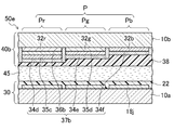
- FIG. 13 is a simplified cross-sectional view of the liquid crystal display panel according to the fifth embodiment.
- FIG. 14 is a cross-sectional view illustrating a part of the manufacturing process of the counter substrate constituting the liquid crystal display panel according to the fifth embodiment.
- FIG. 15 is a simplified cross-sectional view of the liquid crystal display panel according to the sixth embodiment.
- FIG. 16 is a cross-sectional view illustrating a part of the manufacturing process of the counter substrate constituting the liquid crystal display panel according to the sixth embodiment.
- Embodiment 1 of the Invention 1 to 5 show Embodiment 1 of an active matrix substrate and a manufacturing method thereof, a counter substrate and a manufacturing method thereof, and a display panel according to the present invention.
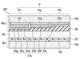
- FIG. 1 is a cross-sectional view of the liquid crystal display panel 50a of the present embodiment
- FIG. 2 is a simplified cross-sectional view of the liquid crystal display panel 50a.
- the liquid crystal display panel 50a is provided as a display medium layer between the active matrix substrate 30a and the counter substrate 40 provided so as to face each other and between the active matrix substrate 30a and the counter substrate 40.
- the liquid crystal layer 45, the active matrix substrate 30a, and the counter substrate 40 are bonded to each other, and a sealing material (not used) is provided in a frame shape to enclose the liquid crystal layer 45 between the active matrix substrate 30a and the counter substrate 40. As shown).
- a plurality of pixels P are provided in a matrix, and in each pixel P, a first sub-pixel Pr that performs red gradation display, a green gradation display.
- the second sub-pixel Pg that performs blue and the third sub-pixel Pb that performs blue gradation display are provided side by side.
- the active matrix substrate 30a includes a substrate 10a, a plurality of gate lines (not shown) provided so as to extend parallel to the substrate 10a, and a direction orthogonal to each gate line.
- a plurality of source lines (not shown) provided so as to extend in parallel with each other, a plurality of TFTs 5 provided for each gate line and each intersection of the source lines, that is, for each subpixel,
- An interlayer insulating film 17 provided so as to cover, a plurality of pixel electrodes 21ra, 21ga and 21ba which are provided on the interlayer insulating film 17 for each of the subpixels Pr, Pg and Pb and arranged in a matrix;
- an alignment film 22 provided so as to cover the pixel electrodes 21ra, 21ga and 21ba.
- the TFT 5 includes a semiconductor layer 12 provided on a substrate 10 a via a base coat film 11, a gate insulating film 13 provided so as to cover the semiconductor layer 12, and a gate insulating film 13 on the gate insulating film 13.
- a gate electrode 14 provided so as to overlap with part of the semiconductor layer 12, a protective insulating film 15 provided so as to cover the gate electrode 14, and provided on the protective insulating film 15 so as to be separated from and opposed to each other.
- a source electrode 16a and a drain electrode 16b are provided.
- the semiconductor layer 12 includes a channel region provided so as to overlap the gate electrode 14 and a source region and a drain region provided so as to be separated from and opposed to each other with the channel region interposed therebetween.
- an LDD (Lightly Doped Drain) region may be provided between the channel region of the semiconductor layer 12 and the source and drain regions.
- the gate electrode 14 is a part or a lateral projecting portion for each of the subpixels Pr, Pg, and Pb in a plurality of gate lines (not shown) provided to extend in parallel with each other on the gate insulating film 13. .
- the source electrode 16a is a part of each of the subpixels Pr, Pg, and Pb in a plurality of source lines (not shown) provided on the protective insulating film 15 so as to extend in parallel to each other in a direction orthogonal to each gate line. It is a protruding part to the side. Further, as shown in FIG. 1, the source electrode 16 a is connected to the source region of the semiconductor layer 12 through a contact hole 15 a formed in the stacked film of the gate insulating film 13 and the protective insulating film 15.
- the drain electrode 16 b is connected to the drain region of the semiconductor layer 12 through a contact hole 15 b formed in the laminated film of the gate insulating film 13 and the protective insulating film 15, and is connected to the interlayer insulating film.
- the pixel electrode 21ra, 21ga or 21ba is connected to the pixel electrode 21a through a contact hole 17a formed in the gate electrode 17a.
- the pixel electrode 21ra provided in the first subpixel Pr includes a first transparent first conductive layer 18a, a second transparent first conductive layer 19a, and the like, which are sequentially stacked from the substrate 10a side.
- a third transparent conductive layer 20a is provided.
- the pixel electrode 21ga provided in the second subpixel Pg includes a first transparent second conductive layer 18b and a second transparent second conductive layer 19b that are sequentially stacked from the substrate 10a side. I have.
- the pixel electrode 21ba provided in the third subpixel Pb is composed of the first transparent third conductive layer 18c as shown in FIGS.
- the counter substrate 40 includes a substrate 10 b, a black matrix 31 provided in a lattice shape on the substrate 10 b, and a first subpixel Pr, a second matrix between each lattice of the black matrix 31.
- a common electrode 34 provided to cover the red layer 32 r, the green layer 32 g and the blue layer 32 b, and an alignment film 38 provided to cover the common electrode 34.
- the liquid crystal layer 45 is made of a nematic liquid crystal material having electro-optical characteristics.
- the liquid crystal display panel 50a having the above configuration is formed on the liquid crystal layer 45 disposed between the pixel electrodes 21ra, 21ga and 21ba on the active matrix substrate 30a and the common electrode 34 on the counter substrate 40 via the alignment films 22 and 38.
- the transmittance of light transmitted through the panel is adjusted for each subpixel Pr, Pg and Pb. And it is comprised so that an image may be displayed.
- the manufacturing method of the liquid crystal display panel 50a of this embodiment includes an active matrix substrate manufacturing process, a counter substrate manufacturing process, and a liquid crystal injection process.
- FIG. 3 is an explanatory view showing a part of the manufacturing process of the active matrix substrate 30a in cross section.
- ⁇ Active matrix substrate manufacturing process First, on the substrate 10a such as a glass substrate, a silicon nitride film, a silicon oxide film, or a laminated film thereof is formed with a thickness of about 200 nm by, for example, a CVD (Chemical Vapor Deposition) method, and the base coat film 11 is formed. Form.
- a CVD Chemical Vapor Deposition
- an intrinsic amorphous silicon film having a thickness of about 50 nm is formed on the entire substrate on which the base coat film 11 is formed, for example, by CVD, and then polycrystallineized by annealing treatment such as laser light irradiation.
- a semiconductor layer 12 is formed by forming a film and subjecting the polysilicon film to photolithography, etching, and resist stripping.
- a silicon nitride film, a silicon oxide film, or a laminated film thereof is formed with a thickness of about 100 nm on the entire substrate on which the semiconductor layer 12 is formed, for example, by a CVD method to form the gate insulating film 13. .
- a metal film such as a molybdenum film with a thickness of about 300 nm on the entire substrate on which the gate insulating film 13 is formed, for example, by sputtering
- the photolithography process and the etching process are performed on the metal film.
- a gate electrode 14 and a gate line are formed.
- an impurity such as phosphorus is implanted into the semiconductor layer 12 on the substrate on which the gate electrode 14 and the like are formed using the gate electrode 14a as a mask, so that a channel region, a source region, and a drain region are formed in the semiconductor layer 12.
- an inorganic insulating film such as a silicon nitride film, a silicon oxide film, or a laminated film thereof is formed on the entire substrate on which the channel region, the source region, and the drain region of the semiconductor layer 12 are formed, for example, by a CVD method.
- the protective insulating film 15 having the contact holes 15a and 15b is formed by performing photolithography processing, etching processing, and resist peeling processing on the inorganic insulating film and the gate insulating film 13 below the inorganic insulating film. Form.
- a metal film in which a titanium film, an aluminum film, a titanium film, and the like are sequentially laminated is formed on the entire substrate on which the protective insulating film 15 is formed, for example, by sputtering, the metal film is formed on the metal film.
- a source electrode 16a, a drain electrode 16b, and a source line are formed by performing a photolithography process, an etching process, and a resist peeling process.
- an acrylic photosensitive resin film is applied to a thickness of about 2 ⁇ m on the entire substrate on which the source electrode 16a, the drain electrode 16b, and the like are formed by, for example, a spin coat method or a slit coat method
- an interlayer insulating film 17 having contact holes 17a is formed by performing pre-baking, exposure, development, and post-baking.
- FIG. 3 (b) the 1st transparent 1st conductive layer 18a, the 1st transparent 2nd conductive layer 18b, and the 1st transparent 3rd conductive layer 18c are formed (1st transparent conductive layer formation process).
- a second transparent layer such as an amorphous ITO film is formed on the entire substrate on which the first transparent first conductive layer 18a, the first transparent second conductive layer 18b, and the first transparent third conductive layer 18c are formed, for example, by sputtering.
- a resist Rab is formed on the second transparent conductive film 19 by exposure to photolithography as shown in FIG. 3C, and is exposed from the resist Rab.
- the second transparent conductive film 19 is etched by polycrystallizing by etching, resist Rab stripping, and annealing, so that the second transparent first conductive layer 19a and the second transparent conductive film 19 are removed.
- the second conductive layer 19b is formed (second transparent conductive layer forming step).
- the third transparent conductive film 20 such as an IZO film is formed to a thickness of about 100 nm on the entire substrate on which the second transparent first conductive layer 19a and the second transparent second conductive layer 19b are formed, for example, by sputtering.
- a photolithography process is performed to form a resist Rac on the third transparent conductive film 20, and an etching process for the third transparent conductive film 20 exposed from the resist Rac.
- the third transparent conductive layer 20a is formed by removing the resist Rac and the pixel electrode 21ra as the first subpixel Pr and the pixel electrode as the second subpixel Pg.
- a pixel electrode 21ba is formed on each of 21ga and the third subpixel Pb (third transparent conductive layer forming step).
- the coating film is baked. Then, the alignment film 22 is formed by performing a rubbing process.
- the active matrix substrate 30a of this embodiment can be manufactured.
- ⁇ Opposite substrate manufacturing process First, after a photosensitive resin colored black is applied to the entire substrate 10b such as a glass substrate by, for example, a spin coating method or a slit coating method, the coating film is exposed and developed, whereby a black matrix is obtained. 31 is formed to a thickness of about 1 ⁇ m.
- a photosensitive resin colored red, green, or blue is applied to the entire substrate on which the black matrix 31 is formed by, for example, spin coating or slit coating, and then the coating film is exposed and developed.
- the colored layer of the selected color for example, the red layer 32r
- the other two colors for example, the green layer 32g and the blue layer 32b
- a thickness of about 1 ⁇ m to 3 ⁇ m is formed.
- a transparent conductive film such as an amorphous ITO film with a thickness of about 100 nm on the entire substrate on which the red layer 32r, the green layer 32g, and the blue layer 32b are formed, for example, by sputtering.
- the common electrode 34 is formed.
- the alignment film 38 is formed.
- the counter substrate 40 of this embodiment can be manufactured.
- a seal material made of UV (ultraviolet) curing and thermosetting resin is printed on the surface of the counter substrate 40 manufactured in the counter substrate manufacturing process in a frame shape, and then a liquid crystal is formed inside the seal material. Drip the material.
- the bonded body is brought to atmospheric pressure. By opening, the surface and the back surface of the bonded body are pressurized.
- the bonded body is heated to cure the seal.
- the unnecessary part is removed by dividing the bonding body which hardened the above-mentioned sealing material, for example by dicing.
- the liquid crystal display panel 50a of the present embodiment can be manufactured.
- FIG. 4 is a graph showing the relationship between the film thickness and transmittance of the transparent conductive film obtained in the experiment of the present embodiment
- FIG. 5 shows the relationship between the film thickness and chromaticity of the transparent conductive film. It is a chromaticity diagram of the CIE 1931 color system showing the relationship.
- “ ⁇ ” indicates the average value of the transmittance data
- a pair of “ ⁇ ” connected by vertical lines indicates the maximum value and the minimum value of the transmittance data.
- IZO films having various film thicknesses (20 nm, 50 nm, 80 nm, 110 nm, 140 nm, 170 nm, and 200 nm) were formed on a glass substrate by a sputtering method, and for each of the formed IZO films, Using a microspectrophotometer (OSP-SP200 manufactured by Olympus Corporation), the transmittance (Y value) and chromaticity (x, y) were measured 5 points at a time.
- OSP-SP200 microspectrophotometer
- the transmittance (Y value) and chromaticity (x, y) change by changing the film thickness of the IZO film.
- the first transparent conductive film, the second transparent conductive film, and the third transparent conductive film are appropriately stacked for each sub-pixel, and the film thickness of the pixel electrode is varied for each sub-pixel. It can be said that desired optical characteristics can be obtained every time.
- the pixel electrode 21ra of the first subpixel Pr is the first transparent conductive layer forming step in the first transparent conductive layer forming step.
- each of the pixel electrodes 21ra, 21ga, and 21ba is formed by appropriately selecting three types of transparent conductive films of the first transparent conductive film 18, the second transparent conductive film 19, and the third transparent conductive film 20.
- three types of dedicated sputtering apparatuses for forming the first transparent conductive film 18, the second transparent conductive film 19, and the third transparent conductive film 20, and the first transparent conductive film 18 and the second transparent conductive film, respectively.
- concentration of processing in a specific sputtering apparatus and the corresponding etching apparatus can be suppressed. Therefore, it is possible to suppress a decrease in manufacturing efficiency of the active matrix substrate 30a. Therefore, in the active matrix substrate 30a and the liquid crystal display panel 50a including the active matrix substrate 30a, it is possible to obtain desired optical characteristics for each of the sub-pixels Pr, Pg, and Pb while suppressing a decrease in manufacturing efficiency.
- the first transparent conductive layer forming step, the second transparent conductive layer forming step, and the third transparent conductive layer forming step are performed in order.
- 18 is a poly-ITO film
- the second transparent conductive film 19 is formed as an amorphous ITO film, patterned and then polycrystallized by annealing
- the third transparent conductive film 20 is an IZO film.
- the first transparent conductive film 18 poly ITO film
- the second transparent conductive film 19 is more resistant to etching than the second transparent conductive film 19 (amorphous ITO film).
- the etching of the first transparent conductive film 18 (first transparent third conductive layer 18c) can be made difficult to progress, and the third transparent conductive layer
- the first transparent conductive film 18 (poly ITO film) and the second transparent conductive film 19 (poly ITO film obtained by polycrystallizing the amorphous ITO film) are used.
- the etching resistance is higher than that of the third transparent conductive film 20 (IZO film)
- the first transparent conductive film 18 (first transparent third conductive layer 18c) and the second transparent conductive film 19 (second transparent second conductive film). The etching of the two conductive layers 19b) can be made difficult to proceed.
- FIG. 6 is a simplified cross-sectional view of the liquid crystal display panel 50b of the present embodiment corresponding to FIG.
- the same portions as those in FIGS. 1 to 5 are denoted by the same reference numerals, and detailed description thereof is omitted.
- the active matrix substrate 30a manufactured by sequentially forming the first transparent conductive film 18, the second transparent conductive film 19, and the third transparent conductive film 20 is exemplified.
- the liquid crystal display panel 50 b includes an active matrix substrate 30 b and a counter substrate 40 provided so as to face each other, and a liquid crystal provided as a display medium layer between the active matrix substrate 30 b and the counter substrate 40.
- a sealing material (not shown) provided in a frame shape for adhering the layer 45 to the active matrix substrate 30b and the counter substrate 40 and enclosing the liquid crystal layer 45 between the active matrix substrate 30b and the counter substrate 40; It has.
- the active matrix substrate 30b includes a substrate 10a, a plurality of gate lines (not shown) provided so as to extend parallel to the substrate 10a, and parallel to each other in a direction orthogonal to the gate lines.
- a plurality of source lines (not shown) provided to extend, a plurality of TFTs (not shown) provided for each gate line and each intersection of the source lines, that is, each subpixel, and each TFT
- An interlayer insulating film 17 (see FIG. 7) provided so as to cover the plurality of pixel electrodes 21rb provided on the interlayer insulating film 17 for each of the subpixels Pr, Pg, and Pb, and arranged in a matrix.
- the configuration between the substrate 10a and the interlayer insulating film 17 is substantially the same as the configuration between the substrate 10a and the interlayer insulating film 17 in the active matrix substrate 30a of the first embodiment. It has become.
- the pixel electrode 21rb provided in the first subpixel Pr includes a third transparent conductive layer 20b, a second transparent first conductive layer 19c, and a first transparent first layer that are sequentially stacked from the substrate 10a side.
- a conductive layer 18d is provided.
- the pixel electrode 21gb provided in the second subpixel Pg includes a second transparent second conductive layer 19d and a first transparent second conductive layer 18e that are sequentially stacked from the substrate 10a side. .
- the pixel electrode 21ba provided in the third subpixel Pb is composed of the first transparent third conductive layer 18f.
- the liquid crystal display panel 50b configured as described above is provided on the liquid crystal layer 45 disposed between the pixel electrodes 21rb, 21gb and 21bb on the active matrix substrate 30b and the common electrode 34 on the counter substrate 40 via the alignment films 22 and 38.
- the transmittance of light transmitted through the panel is adjusted for each subpixel Pr, Pg and Pb. And it is comprised so that an image may be displayed.
- the manufacturing method of the liquid crystal display panel 50b of this embodiment includes an active matrix substrate manufacturing process, a counter substrate manufacturing process, and a liquid crystal injection process.
- the counter substrate manufacturing process and the liquid crystal injection process are substantially the same as those in the first embodiment. Therefore, the active matrix substrate manufacturing process will be described below with reference to FIG.
- FIG. 7 is an explanatory view showing, in section, a part of the manufacturing process of the active matrix substrate 30b.
- the layers up to the interlayer insulating film 17 are formed by the same method as in the first embodiment, and the third transparent conductive film 20 such as a poly ITO film is formed on the entire substrate on which the interlayer insulating film 17 has been formed, for example, by sputtering.
- the film with a thickness of about 100 nm as shown in FIG. 7A, a photolithography process is performed to form a resist Rba on the third transparent conductive film 20, and the third transparent conductive exposed from the resist Rba.
- the third transparent conductive layer 20b is formed as shown in FIG. 7B (third transparent conductive layer forming step).
- FIG. 4 a resist Rbb is formed on the second transparent conductive film 19 by performing a photolithography process, and the etching process, the resist Rbb peeling process, and the annealing process for the second transparent conductive film 19 exposed from the resist Rbb.
- the second transparent first conductive layer 19c and the second transparent second conductive layer 19d are formed (second transparent conductive layer forming step).
- the first transparent conductive film 18 such as an IZO film is formed with a thickness of about 100 nm on the entire substrate on which the second transparent first conductive layer 19c and the second transparent second conductive layer 19d are formed, for example, by sputtering.
- a photolithography process is performed to form a resist Rbc on the first transparent conductive film 18, and an etching process for the first transparent conductive film 18 exposed from the resist Rbc.
- the first transparent first conductive layer 18d, the first transparent second conductive layer 18e, and the first transparent third conductive layer 18f are formed by performing the peeling process of the resist Rbc as shown in FIG.
- the pixel electrode 21rb is formed on the first subpixel Pr
- the pixel electrode 21gb is formed on the second subpixel Pg
- the pixel electrode 21bb is formed on the third subpixel Pb (first transparent conductive layer forming process).
- a polyimide resin film is applied to the entire substrate on which the pixel electrodes 21rb, 21gb, and 21bb are formed by, for example, a spin coating method, a slit coating method, or a printing method, and then the coating film is baked. Then, the alignment film 22 is formed by performing a rubbing process.
- the active matrix substrate 30b of this embodiment can be manufactured.
- the pixel electrode 21rb of the first subpixel Pr is the first transparent conductive layer forming step in the first transparent conductive layer forming step.
- each of the pixel electrodes 21rb, 21gb, and 21bb is formed by appropriately selecting three types of transparent conductive films of the first transparent conductive film 18, the second transparent conductive film 19, and the third transparent conductive film 20.
- three types of dedicated sputtering apparatuses for forming the first transparent conductive film 18, the second transparent conductive film 19, and the third transparent conductive film 20, and the first transparent conductive film 18 and the second transparent conductive film, respectively.
- concentration of processing in a specific sputtering apparatus and the corresponding etching apparatus can be suppressed. Therefore, it is possible to suppress a decrease in manufacturing efficiency of the active matrix substrate 30b. Therefore, in the active matrix substrate 30b and the liquid crystal display panel 50b including the active matrix substrate 30b, it is possible to obtain desired optical characteristics for each of the subpixels Pr, Pg, and Pb while suppressing a decrease in manufacturing efficiency.
- FIG. 8 is a simplified cross-sectional view of the liquid crystal display panel 50c of the present embodiment corresponding to FIG. 2 and FIG.
- an active matrix substrate 30a manufactured by sequentially forming the first transparent conductive film 18, the second transparent conductive film 19, and the third transparent conductive film 20 is illustrated.
- the first the active matrix substrate 30b manufactured by sequentially forming the third transparent conductive film 20, the second transparent conductive film 19, and the first transparent conductive film 18 is illustrated, in the present embodiment, the second transparent conductive film 19,
- An active matrix substrate 30c manufactured by sequentially forming three transparent conductive films 20 and a first transparent conductive film 18 is illustrated.
- the liquid crystal display panel 50c includes an active matrix substrate 30c and a counter substrate 40 provided so as to face each other, and a liquid crystal provided as a display medium layer between the active matrix substrate 30c and the counter substrate 40.
- a sealing material (not shown) provided in a frame shape for adhering the layer 45 to the active matrix substrate 30c and the counter substrate 40 and enclosing the liquid crystal layer 45 between the active matrix substrate 30c and the counter substrate 40; It has.
- the active matrix substrate 30c includes a substrate 10a, a plurality of gate lines (not shown) provided so as to extend parallel to the substrate 10a, and parallel to each other in a direction orthogonal to the gate lines.
- a plurality of source lines (not shown) provided to extend, a plurality of TFTs (not shown) provided for each gate line and each intersection of the source lines, that is, each subpixel, and each TFT
- An interlayer insulating film 17 (see FIG. 9) provided so as to cover the plurality of pixel electrodes 21rc provided on the interlayer insulating film 17 for each of the subpixels Pr, Pg, and Pb and arranged in a matrix.
- the configuration between the substrate 10a and the interlayer insulating film 17 is substantially the same as the configuration between the substrate 10a and the interlayer insulating film 17 in the active matrix substrate 30a of the first embodiment. It has become.
- the pixel electrode 21rc provided in the first subpixel Pr includes a second transparent first conductive layer 19e, a third transparent conductive layer 20c, and a first transparent first layer stacked in order from the substrate 10a side.
- One conductive layer 18g is provided.
- the pixel electrode 21gc provided in the second subpixel Pg includes a second transparent second conductive layer 19f and a first transparent second conductive layer 18h that are sequentially stacked from the substrate 10a side. .
- the pixel electrode 21bc provided in the third subpixel Pb is composed of the first transparent third conductive layer 18i as shown in FIG.
- the liquid crystal display panel 50c having the above configuration is formed on the liquid crystal layer 45 disposed between the pixel electrodes 21rc, 21gc and 21bc on the active matrix substrate 30c and the common electrode 34 on the counter substrate 40 via the alignment films 22 and 38.
- the transmittance of light transmitted through the panel is adjusted for each subpixel Pr, Pg and Pb. And it is comprised so that an image may be displayed.
- the manufacturing method of the liquid crystal display panel 50c of this embodiment includes an active matrix substrate manufacturing process, a counter substrate manufacturing process, and a liquid crystal injection process.
- the counter substrate manufacturing process and the liquid crystal injection process are substantially the same as those in the first embodiment.
- an active matrix substrate manufacturing process will be described with reference to FIG.
- FIG. 9 is an explanatory view showing a part of the manufacturing process of the active matrix substrate 30c in cross section.
- the layers up to the interlayer insulating film 17 are formed by the same method as in the first embodiment, and the third transparent conductive film 19 such as a poly ITO film is formed on the entire substrate on which the interlayer insulating film 17 is formed, for example, by sputtering.
- the film with a thickness of about 100 nm as shown in FIG. 9A, a photolithography process is performed to form a resist Rca on the second transparent conductive film 19, and the second transparent conductive exposed from the resist Rca.
- the second transparent first conductive layer 19e and the second transparent second conductive layer 19f are formed as shown in FIG. Transparent conductive layer forming step).
- a third transparent conductive film 20 such as an amorphous ITO film is formed on the entire substrate on which the second transparent first conductive layer 19e and the second transparent second conductive layer 19f are formed by a sputtering method, for example, to a thickness of about 100 nm.
- the resist Rcb is formed on the third transparent conductive film 20 by performing a photolithography process as shown in FIG. 9C, and the third transparent conductive film 20 exposed from the resist Rcb is etched.
- the third transparent conductive layer 20c is formed by performing polycrystallization by the treatment, the resist Rcb peeling treatment, and the annealing treatment (third transparent conductive layer forming step).
- the first transparent conductive film 18 such as an IZO film with a thickness of about 100 nm on the entire substrate on which the third transparent conductive layer 20c has been formed by, for example, sputtering
- a resist Rcc is formed on the first transparent conductive film 18 by performing a photolithography process, an etching process on the first transparent conductive film 18 exposed from the resist Rcc, and a stripping process of the resist Rcc are performed.
- the first transparent first conductive layer 18g, the first transparent second conductive layer 18h, and the first transparent third conductive layer 18i are formed, and the pixel electrode 21rc is formed on the first subpixel Pr.
- the pixel electrode 21gc is formed on the second subpixel Pg
- the pixel electrode 21bc is formed on the third subpixel Pb (first transparent conductive layer forming step).
- the coating film is baked. Then, the alignment film 22 is formed by performing a rubbing process.
- the active matrix substrate 30c of this embodiment can be manufactured.
- the pixel electrode 21rc of the first subpixel Pr is the first transparent conductive layer forming step.
- each of the pixel electrodes 21rc, 21gc, and 21bc is formed by appropriately selecting three types of transparent conductive films, the first transparent conductive film 18, the second transparent conductive film 19, and the third transparent conductive film 20.
- FIG. 10 is a cross-sectional view of the liquid crystal display panel 50d of this embodiment
- FIG. 11 is a simplified cross-sectional view of the liquid crystal display panel 50d.
- liquid crystal display panels 50a to 50c including the active matrix substrates 30a to 30c in which the film thickness of the pixel electrode is different for each sub-pixel are illustrated.
- the liquid crystal display panel 50d is provided as a display medium layer between the active matrix substrate 30 and the counter substrate 40a provided so as to face each other and between the active matrix substrate 30 and the counter substrate 40a.
- the liquid crystal layer 45, the active matrix substrate 30 and the counter substrate 40a are bonded to each other, and a sealing material (not used) is provided in a frame shape to enclose the liquid crystal layer 45 between the active matrix substrate 30 and the counter substrate 40a. As shown).
- the active matrix substrate 30 includes a substrate 10a, a plurality of gate lines (not shown) provided so as to extend parallel to the substrate 10a, and a direction orthogonal to each gate line.
- a plurality of source lines (not shown) provided so as to extend in parallel with each other, a plurality of TFTs 5 provided for each gate line and each intersection of the source lines, that is, for each subpixel,
- An interlayer insulating film 17 provided so as to cover, a plurality of pixel electrodes 18j provided on the interlayer insulating film 17 for each of the subpixels Pr, Pg, and Pb, arranged in a matrix, and each pixel electrode 18j And an alignment film 22 provided so as to cover it.
- the configuration between the substrate 10a and the interlayer insulating film 17 is substantially the same as the configuration between the substrate 10a and the interlayer insulating film 17 in the active matrix substrate 30a of the first embodiment. It has become.
- the drain electrode 16b of the TFT 5 is connected to the pixel electrode 18j through a contact hole 17a formed in the interlayer insulating film 17, as shown in FIG.
- the counter substrate 40 a includes a substrate 10 b, a black matrix 31 provided in a lattice pattern on the substrate 10 b, and a first subpixel Pr and a second subspace between the lattices of the black matrix 31.
- a common electrode 37a provided so as to cover the red layer 32r, the green layer 32g, and the blue layer 32b, and an alignment film 38 provided so as to cover the common electrode 37a.
- the common electrode 37 a includes a first transparent first conductive layer 34 a, a second transparent first conductive layer 35 a, and a third layer stacked in order from the substrate 10 b side in the first subpixel Pr.
- the second subpixel Pg has a transparent conductive layer 36a, and has a first transparent second conductive layer 34b and a second transparent second conductive layer 35b, which are sequentially stacked from the substrate 10b side.
- the first transparent third conductive layer 34c is provided in the third subpixel Pb.
- the first transparent first conductive layer 34a, the first transparent second conductive layer 34b, and the first transparent third conductive layer 34c are formed integrally with each other. It is connected.
- the second transparent first conductive layer 35a and the second transparent second conductive layer 35b are formed independently, but the second transparent first conductive layer 35a and the second transparent second conductive layer are formed.
- the 35b may be formed integrally, and when the second transparent first conductive layer 35a and the second transparent second conductive layer 35b are formed integrally, the first transparent first conductive layer 34a. And the 1st transparent 2nd conductive layer 34b does not need to be formed integrally.
- the liquid crystal display panel 50d having the above configuration has each subpixel Pr in the liquid crystal layer 45 disposed via the alignment films 22 and 38 between each pixel electrode 18j on the active matrix substrate 30 and the common electrode 37a on the counter substrate 40a.
- the transmittance of light transmitted through the panel is adjusted for each subpixel Pr, Pg and Pb, and an image is obtained. Is configured to display.
- the manufacturing method of the liquid crystal display panel 50d of this embodiment includes an active matrix substrate manufacturing process, a counter substrate manufacturing process, and a panel manufacturing process, but the liquid crystal injection process is substantially the same as in the first embodiment. Therefore, hereinafter, the active matrix substrate manufacturing process and the counter substrate manufacturing process will be described with reference to FIGS.
- FIG. 12 is explanatory drawing which shows a part of manufacturing process of the opposing board
- substrate 40a in FIGS. 11 and 12 (f)
- the configuration of the counter substrate 40a is illustrated as being reversed left and right, but both are substantially the same.
- the interlayer insulating film 17 is formed by the same method as in the first embodiment, and a transparent conductive film such as an amorphous ITO film is formed to a thickness of 100 nm on the entire substrate on which the interlayer insulating film 17 is formed by, for example, sputtering.
- a pixel electrode 18j is formed by performing a photolithography process, an etching process, and a resist peeling process on the transparent conductive film.
- the coating film is subjected to baking and rubbing treatment. Thereby, the alignment film 22 is formed.
- the active matrix substrate 30 of this embodiment can be manufactured.
- the red layer 32r, the green layer 32g, and the blue layer 32b are formed by the same method as in the first embodiment, and the color filter 32 including the red layer 32r, the green layer 32g, and the blue layer 32b is formed on the entire substrate.
- the first transparent conductive film 34 such as a poly ITO film is formed with a thickness of about 100 nm by sputtering
- the first transparent conductive film is subjected to photolithography as shown in FIG.
- a resist Rda is formed on the film 34, an etching process is performed on the first transparent conductive film 34 exposed from the resist Rda, and a peeling process of the resist Rda is performed, as shown in FIG.
- the first conductive layer 34a, the first transparent second conductive layer 34b, and the first transparent third conductive layer 34c are integrally formed (first transparent conductive layer forming step).
- the second substrate such as an amorphous ITO film is formed on the entire substrate on which the first transparent first conductive layer 34a, the first transparent second conductive layer 34b, and the first transparent third conductive layer 34c are formed, for example, by sputtering.
- a resist Rdb is formed on the second transparent conductive film 35 by performing a photolithography process and exposed from the resist Rdb.
- the second transparent conductive film 35 and the second transparent conductive film 35 are subjected to an etching process, a resist Rdb peeling process, and an annealing process to perform crystallization.
- the transparent second conductive layer 35b is formed (second transparent conductive layer forming step).
- a third transparent conductive film 36 such as an IZO film is formed to a thickness of about 100 nm on the entire substrate on which the second transparent first conductive layer 35a and the second transparent second conductive layer 35b are formed, for example, by sputtering.
- a photolithography process is performed to form a resist Rdc on the third transparent conductive film 36, and an etching process for the third transparent conductive film 36 exposed from the resist Rdc.
- the third transparent conductive layer 36a is formed and the common electrode 37a is formed (third transparent conductive layer forming step).
- the coating film is subjected to baking and rubbing treatment. By doing so, the alignment film 38 is formed.
- the counter substrate 40a of this embodiment can be manufactured.
- the common electrode 37a is the first transparent conductive layer forming step in the first sub-pixel Pr.
- a first transparent first conductive layer 34a formed by patterning the conductive film 34; a second transparent first conductive layer 35a formed by patterning the second transparent conductive film 35 in the second transparent conductive layer forming step; and It has the 3rd transparent conductive layer 36a formed by patterning the 3rd transparent conductive film 36 at the 3rd transparent conductive layer formation process, and in the 2nd subpixel Pg, the 1st transparent conductive layer at the 1st transparent conductive layer formation process
- a first transparent second conductive layer 34b formed by patterning the film 34, and a second transparent second conductive layer 35b formed by patterning the second transparent conductive film 35 in the second transparent conductive layer forming step.
- the sub-pixel Pb includes a first transparent third conductive layer 34c formed by patterning the first transparent conductive film 34 in the first transparent conductive layer forming step, and includes a first transparent first conductive layer 34a and a first transparent conductive layer 34c. Since the second conductive layer 34b and the first transparent third conductive layer 34c are integrally formed, the common electrode 37a is specifically formed, and the film thickness of the common electrode 37a in each of the subpixels Pr, Pg, and Pb is the first thickness. The first subpixel Pr, the second subpixel Pg, and the third subpixel Pb become thinner in this order.
- the common electrode 37a has different thicknesses in the first subpixel Pr, the second subpixel Pg, and the third subpixel Pb, each subpixel Pr, Pg, and Pb in the counter substrate 40a. Desired optical characteristics can be obtained for each time.
- the common electrode 37a is formed by appropriately selecting three types of transparent conductive films of the first transparent conductive film 34, the second transparent conductive film 35, and the third transparent conductive film 36, for example, the first transparent conductive film 37a Three types of dedicated sputtering apparatuses for forming the transparent conductive film 34, the second transparent conductive film 35, and the third transparent conductive film 36, and the first transparent conductive film 34, the second transparent conductive film 35, and the third transparent conductive film 34, respectively.
- the concentration of processing in a specific sputtering apparatus and the corresponding etching apparatus can be suppressed.
- a decrease in production efficiency can be suppressed. Therefore, in the counter substrate 40a, it is possible to obtain desired optical characteristics for each of the subpixels Pr, Pg, and Pb while suppressing a decrease in manufacturing efficiency.
- the first transparent conductive layer 34 is sequentially performed by performing the first transparent conductive layer forming step, the second transparent conductive layer forming step, and the third transparent conductive layer forming step.
- the second transparent conductive film 35 is formed as an amorphous ITO film, patterned and then polycrystallized by annealing, and the third transparent conductive film 36 is an IZO film.
- the first transparent conductive film 34 (poly ITO film) has higher etching resistance than the second transparent conductive film 35 (amorphous ITO film).
- the etching of the first transparent conductive film 34 (first transparent third conductive layer 34c) can be made difficult to progress, and in the third transparent conductive layer forming step,
- the first transparent conductive film 34 (poly-ITO film) and the second transparent conductive film 35 (poly-ITO film obtained by polycrystallizing the amorphous ITO film) are third transparent. Since the etching resistance is higher than that of the conductive film 36 (IZO film), the first transparent conductive film 34 (first transparent third conductive layer 34c) and the second transparent conductive film 35 (second transparent second conductive layer 35b). ) Etching can be made difficult to proceed.
- FIG. 13 is a simplified cross-sectional view of the liquid crystal display panel 50e of the present embodiment corresponding to FIG.
- the counter substrate 40a manufactured by sequentially forming the first transparent conductive film 34, the second transparent conductive film 35, and the third transparent conductive film 36 is exemplified.
- the counter substrate 40b manufactured by sequentially forming the transparent conductive film 36, the second transparent conductive film 35, and the first transparent conductive film 34 is illustrated.
- the liquid crystal display panel 50e includes an active matrix substrate 30 and a counter substrate 40b provided so as to face each other, and a liquid crystal provided as a display medium layer between the active matrix substrate 30 and the counter substrate 40b.
- a sealing material (not shown) provided in a frame shape for adhering the layer 45 to the active matrix substrate 30 and the counter substrate 40b and enclosing the liquid crystal layer 45 between the active matrix substrate 30 and the counter substrate 40b; It has.
- the counter substrate 40b includes a substrate 10b, a black matrix 31 (see FIG. 10) provided in a lattice pattern on the substrate 10b, and a first subpixel Pr, A red layer 32r, a green layer 32g, and a blue layer 32b provided as a first colored layer, a second colored layer, and a third colored layer, respectively, so as to correspond to the second subpixel Pg and the third subpixel Pb;
- a common electrode 37b is provided so as to cover the black matrix 31, the red layer 32r, the green layer 32g and the blue layer 32b, and an alignment film 38 is provided so as to cover the common electrode 37b.
- the common electrode 37b includes a third transparent conductive layer 36b, a second transparent first conductive layer 35c, and a first transparent first conductive layer, which are sequentially stacked from the substrate 10b side.
- the second subpixel Pg includes a second transparent second conductive layer 35d and a first transparent second conductive layer 34e stacked in order from the substrate 10b side.
- It has a transparent third conductive layer 34f.
- First transparent first conductive layer 34d, first transparent second conductive layer 34e, first transparent third conductive layer 34f, second transparent first conductive layer 35c, second transparent second conductive layer 35d, and third transparent conductive layer As shown in FIG. 13, the first transparent first conductive layer 34d, the first transparent second conductive layer 34e, and the first transparent third conductive layer 34f are integrally formed as shown in FIG. Yes.
- the liquid crystal display panel 50e having the above configuration has each subpixel Pr in the liquid crystal layer 45 disposed via the alignment films 22 and 38 between each pixel electrode 18j on the active matrix substrate 30 and the common electrode 37b on the counter substrate 40b.
- the transmittance of light transmitted through the panel is adjusted for each subpixel Pr, Pg and Pb, and an image is obtained. Is configured to display.
- the manufacturing method of the liquid crystal display panel 50e of the present embodiment includes an active matrix substrate manufacturing process, a counter substrate manufacturing process, and a liquid crystal injection process.
- the active matrix substrate manufacturing process and the liquid crystal injection process are the same as those in the fourth embodiment. Since it is substantially the same, the counter substrate manufacturing process will be described below with reference to FIG.
- FIG. 14 is explanatory drawing which shows a part of manufacturing process of the opposing board
- FIG. 13 and FIG. 14 (f) the configuration of the counter substrate 40 b is illustrated as being reversed left and right, but both are substantially the same.
- the red layer 32r, the green layer 32g, and the blue layer 32b are formed by the same method as in the first embodiment, and the color filter 32 including the red layer 32r, the green layer 32g, and the blue layer 32b is formed on the entire substrate.
- the third transparent conductive film 36 such as a poly ITO film with a thickness of about 100 nm by sputtering, for example, as shown in FIG.
- a resist Rea is formed on the film 36
- an etching process is performed on the third transparent conductive film 36 exposed from the resist Re, and a peeling process of the resist Re is performed, as shown in FIG.
- the layer 36b is formed (third transparent conductive layer forming step).
- FIG. 5 a resist Reb is formed on the second transparent conductive film 35 by performing a photolithography process, and an etching process, a resist Reb stripping process, and an annealing process on the second transparent conductive film 35 exposed from the resist Reb As shown in FIG. 14D, the second transparent first conductive layer 35c and the second transparent second conductive layer 35d are formed (second transparent conductive layer forming step).
- the first transparent conductive film 34 such as an IZO film is formed to a thickness of about 100 nm on the entire substrate on which the second transparent first conductive layer 35c and the second transparent second conductive layer 35d are formed, for example, by sputtering.
- a resist Rec is formed on the first transparent conductive film 34 by performing a photolithography process, and an etching process for the first transparent conductive film 34 exposed from the resist Rec.
- the first transparent first conductive layer 34d, the first transparent second conductive layer 34e, and the first transparent third conductive layer 34f are integrally formed by performing the resist Rec peeling process.
- the common electrode 37b is formed (first transparent conductive layer forming step).
- the coating film is baked and rubbed. By doing so, the alignment film 38 is formed.
- the counter substrate 40b of this embodiment can be manufactured.
- the common electrode 37b is the first transparent conductive layer forming step in the first sub-pixel Pr.
- the sub-pixel Pb includes a first transparent third conductive layer 34f formed by patterning the first transparent conductive film 34 in the first transparent conductive layer forming step, and includes a first transparent first conductive layer 34d and a first transparent conductive layer 34d. Since the second conductive layer 34e and the first transparent third conductive layer 34f are integrally formed, the common electrode 37b is specifically formed, and the film thickness of the common electrode 37b in each of the subpixels Pr, Pg, and Pb is the first thickness. The first subpixel Pr, the second subpixel Pg, and the third subpixel Pb become thinner in this order.
- the common electrode 37b has different thicknesses in the first subpixel Pr, the second subpixel Pg, and the third subpixel Pb, each subpixel Pr, Pg, and Pb in the counter substrate 40b. Desired optical characteristics can be obtained for each time.
- the common electrode 37b is formed by appropriately selecting three types of transparent conductive films of the first transparent conductive film 34, the second transparent conductive film 35, and the third transparent conductive film 36, for example, the first transparent conductive film 37b Three types of dedicated sputtering apparatuses for forming the transparent conductive film 34, the second transparent conductive film 35, and the third transparent conductive film 36, and the first transparent conductive film 34, the second transparent conductive film 35, and the third transparent conductive film 34, respectively.
- the concentration of processing in a specific sputtering apparatus and the corresponding etching apparatus can be suppressed.
- a decrease in production efficiency can be suppressed. Therefore, in the counter substrate 40b, it is possible to obtain desired optical characteristics for each of the subpixels Pr, Pg, and Pb while suppressing a decrease in manufacturing efficiency.
- FIG. 15 is a simplified cross-sectional view of the liquid crystal display panel 50f of the present embodiment corresponding to FIG. 11 and FIG.
- the counter substrate 40a manufactured by sequentially forming the first transparent conductive film 34, the second transparent conductive film 35, and the third transparent conductive film 36 is illustrated.
- the third substrate Although the counter substrate 40b manufactured by sequentially forming the transparent conductive film 36, the second transparent conductive film 35, and the first transparent conductive film 34 is illustrated, in the present embodiment, the second transparent conductive film 35 and the third transparent conductive film 34 are illustrated.
- the counter substrate 40c manufactured by sequentially forming the conductive film 36 and the first transparent conductive film 34 is illustrated.
- the liquid crystal display panel 50f includes an active matrix substrate 30 and a counter substrate 40c provided so as to face each other, and a liquid crystal provided as a display medium layer between the active matrix substrate 30 and the counter substrate 40c.
- a sealing material (not shown) provided in a frame shape for adhering the layer 45 to the active matrix substrate 30 and the counter substrate 40c and enclosing the liquid crystal layer 45 between the active matrix substrate 30 and the counter substrate 40c; It has.
- the counter substrate 40c includes a substrate 10b, a black matrix 31 (see FIG. 10) provided in a lattice pattern on the substrate 10b, and a first subpixel Pr, A red layer 32r, a green layer 32g, and a blue layer 32b provided as a first colored layer, a second colored layer, and a third colored layer, respectively, so as to correspond to the second subpixel Pg and the third subpixel Pb;
- a common electrode 37c is provided so as to cover the black matrix 31, the red layer 32r, the green layer 32g, and the blue layer 32b, and an alignment film 38 is provided so as to cover the common electrode 37c.
- the common electrode 37c includes a second transparent first conductive layer 35e, a third transparent conductive layer 36c, and a first transparent first conductive layer that are sequentially stacked from the substrate 10b side.
- the second subpixel Pg includes a second transparent second conductive layer 35f and a first transparent second conductive layer 34h, which are sequentially stacked from the substrate 10b side.
- the third subpixel Pb It has a transparent third conductive layer 34i.
- the first transparent first conductive layer 34g, the first transparent second conductive layer 34h, the first transparent third conductive layer 34i, the second transparent first conductive layer 35e, the second transparent second conductive layer 35f, and the third transparent conductive layer As shown in FIG. 15, the first transparent first conductive layer 34g, the first transparent second conductive layer 34h, and the first transparent third conductive layer 34i are integrally formed as shown in FIG. Yes.
- the liquid crystal display panel 50f having the above configuration has each subpixel Pr in the liquid crystal layer 45 disposed via the alignment films 22 and 38 between each pixel electrode 18j on the active matrix substrate 30 and the common electrode 37c on the counter substrate 40c.
- the transmittance of light transmitted through the panel is adjusted for each subpixel Pr, Pg and Pb, and an image is obtained. Is configured to display.
- the manufacturing method of the liquid crystal display panel 50f of the present embodiment includes an active matrix substrate manufacturing process, a counter substrate manufacturing process, and a liquid crystal injection process.
- the active matrix substrate manufacturing process and the liquid crystal injection process are the same as those in the fourth embodiment. Since it is substantially the same, the counter substrate manufacturing process will be described below with reference to FIG.
- FIG. 16 is explanatory drawing which shows a part of manufacturing process of the opposing board
- the red layer 32r, the green layer 32g, and the blue layer 32b are formed by the same method as in the first embodiment, and the color filter 32 including the red layer 32r, the green layer 32g, and the blue layer 32b is formed on the entire substrate.
- the second transparent conductive film 35 such as a poly ITO film is formed with a thickness of about 100 nm by sputtering
- the second transparent conductive film is subjected to photolithography as shown in FIG.
- a resist Rfa is formed on the film 35, an etching process is performed on the second transparent conductive film 35 exposed from the resist Rfa, and a resist Re peeling process is performed, as shown in FIG.
- the first conductive layer 35e and the second transparent second conductive layer 35f are formed (second transparent conductive layer forming step).
- a third transparent conductive film 36 such as an amorphous ITO film is formed on the entire substrate on which the second transparent first conductive layer 35e and the second transparent second conductive layer 35f are formed by a sputtering method, for example, to a thickness of about 100 nm.
- the resist Rfb is formed on the third transparent conductive film 36 by performing a photolithography process as shown in FIG. 16C, and the third transparent conductive film 36 exposed from the resist Rfb is etched.
- the third transparent conductive layer 36c is formed as shown in FIG. 16 (d) by performing polycrystallization by the process, the resist Rfb peeling process, and the annealing process (third transparent conductive layer forming step).
- a first transparent conductive film 34 such as an IZO film with a thickness of about 100 nm on the entire substrate on which the third transparent conductive layer 36c is formed, for example, by sputtering, as shown in FIG.
- a resist Rfc is formed on the first transparent conductive film 34 by performing a photolithography process, an etching process on the first transparent conductive film 34 exposed from the resist Rfc, and a stripping process of the resist Rfc are performed.
- the first transparent first conductive layer 34g, the first transparent second conductive layer 34h, and the first transparent third conductive layer 34i are integrally formed to form a common electrode 37c (see FIG. 16F).
- First transparent conductive layer forming step ).
- the coating film is subjected to baking and rubbing treatment. By doing so, the alignment film 38 is formed.
- the counter substrate 40c of this embodiment can be manufactured.
- the common electrode 37c is the first transparent conductive layer forming step in the first sub-pixel Pr.
- a first transparent first conductive layer 34g formed by patterning the conductive film 34, a second transparent first conductive layer 35e formed by patterning the second transparent conductive film 35 in the second transparent conductive layer forming step, and It has the 3rd transparent conductive layer 36c formed by patterning the 3rd transparent conductive film 36 at the 3rd transparent conductive layer formation process, and in the 2nd subpixel Pg, the 1st transparent conductive layer at the 1st transparent conductive layer formation process
- a first transparent second conductive layer 34h formed by patterning the film 34, and a second transparent second conductive layer 35f formed by patterning the second transparent conductive film 35 in the second transparent conductive layer forming step.
- the sub-pixel Pb has a first transparent third conductive layer 34i formed by patterning the first transparent conductive film 34 in the first transparent conductive layer forming step, and includes a first transparent first conductive layer 34g and a first transparent conductive layer 34g. Since the second conductive layer 34h and the first transparent third conductive layer 34i are integrally formed, the common electrode 37c is specifically formed, and the film thickness of the common electrode 37c in each of the subpixels Pr, Pg, and Pb is The first subpixel Pr, the second subpixel Pg, and the third subpixel Pb become thinner in this order.
- the common electrode 37c has different thicknesses in the first subpixel Pr, the second subpixel Pg, and the third subpixel Pb, each subpixel Pr, Pg, and Pb in the counter substrate 40c. Desired optical characteristics can be obtained for each time.
- the common electrode 37c is formed by appropriately selecting three types of transparent conductive films of the first transparent conductive film 34, the second transparent conductive film 35, and the third transparent conductive film 36, for example, the first transparent conductive film 37c, Three types of dedicated sputtering apparatuses for forming the transparent conductive film 34, the second transparent conductive film 35, and the third transparent conductive film 36, and the first transparent conductive film 34, the second transparent conductive film 35, and the third transparent conductive film 34, respectively.
- the concentration of processing in a specific sputtering apparatus and the corresponding etching apparatus can be suppressed.
- a decrease in production efficiency can be suppressed. Therefore, in the counter substrate 40c, it is possible to obtain desired optical characteristics for each of the subpixels Pr, Pg, and Pb while suppressing a decrease in manufacturing efficiency.
- the pixel electrode or common electrode in the first subpixel Pr that performs red gradation display is relatively thick
- the pixel electrode or common in the third subpixel Pb that performs blue gradation display is relatively thick.
- the configuration in which the electrodes are relatively thin has been exemplified, but the present invention is not limited to this configuration (combination of film thicknesses).
- liquid crystal display panel in which the sub-pixel arrangement is a stripe arrangement is illustrated, but the present invention is also applied to a display panel in which the sub-pixel arrangement is a delta arrangement, a mosaic arrangement, or the like. be able to.
- the liquid crystal display panel in which each pixel has the first subpixel, the second subpixel, and the third subpixel has been exemplified.
- the present invention increases each type of transparent conductive film, The present invention can also be applied to a display panel in which a pixel has four or more subpixels.
- this invention is the 1st colored layer, the 2nd colored layer.
- the present invention can also be applied to a display panel having a color filter on array structure in which the layer and the third colored layer are provided on the active matrix substrate side.
- a liquid crystal display panel is exemplified as the display panel.
- the present invention can also be applied to other display panels such as an organic EL (Electro Luminescence) panel.
- an active matrix substrate in which a TFT electrode connected to a pixel electrode is used as a drain electrode is exemplified.
- an active matrix in which a TFT electrode connected to a pixel electrode is referred to as a source electrode. It can also be applied to a substrate.
- the present invention is useful for a display panel such as a liquid crystal display panel or an organic EL panel because desired optical characteristics can be obtained for each sub-pixel while suppressing a decrease in manufacturing efficiency. .
Landscapes
- Physics & Mathematics (AREA)
- Nonlinear Science (AREA)
- Mathematical Physics (AREA)
- Chemical & Material Sciences (AREA)
- Crystallography & Structural Chemistry (AREA)
- General Physics & Mathematics (AREA)
- Optics & Photonics (AREA)
- Liquid Crystal (AREA)
- Devices For Indicating Variable Information By Combining Individual Elements (AREA)
Abstract
基板(10a)にマトリクス状に設けられた複数の画素電極(21ra、21ga、21ba)を備え、各画素電極に対応して、互いに異なる色を表示するための第1副画素(Pr)、第2副画素(Pg)及び第3副画素(Pb)が規定されたアクティブマトリクス基板(30a)であって、第1副画素(Pr)の画素電極(21ra)は、第1透明導電膜により形成された第1透明第1導電層(18a)、第2透明導電膜により形成された第2透明第1導電層(19a)、及び第3透明導電膜により形成された第3透明導電層(20a)を有し、第2副画素(Pg)の画素電極(21ga)は、第1透明導電膜により形成された第1透明第2導電層(18b)、及び第2透明導電膜により形成された第2透明第2導電層(19b)を有し、第3副画素(Pb)の画素電極(21ba)は、第1透明導電膜により形成された第1透明第3導電層(18c)を有している。
Description
本発明は、アクティブマトリクス基板及びその製造方法、対向基板及びその製造方法、並びに表示パネルに関し、特に、アクティブマトリクス基板における画素電極や対向基板における共通電極の構成及びその形成方法に関するものである。
液晶表示パネルは、例えば、画像の最小単位である各副画素毎に薄膜トランジスタ(Thin Film Transistor、以下、「TFT」とも称する)や画素電極などが設けられたアクティブマトリクス基板と、アクティブマトリクス基板に対向して配置され、共通電極などが設けられた対向基板と、アクティブマトリクス基板及び対向基板の間に封入された液晶層とを備えている。
対向基板は、例えば、ガラス基板上に格子状に設けられたブラックマトリクスと、ブラックマトリクスの各格子間、すなわち、各副画素毎にそれぞれ設けられた赤色層、緑色層及び青色層などからなる複数の着色層と、ブラックマトリクス及び各着色層を覆うように設けられた共通電極とを備えている。
上記構成の対向基板においては、共通電極がスパッタリング法により成膜された透明導電膜により形成されるので、例えば、赤色層が設けられた赤色の階調表示を行う副画素、緑色層が設けられた緑色の階調表示を行う副画素、及び青色層が設けられた青色の階調表示を行う副画素における共通電極の各膜厚が基板面内で同じになり、各副画素毎に所望の光学特性を得ることが困難である。また、上記構成のアクティブマトリクス基板においても、各画素電極がスパッタリング法により成膜された透明導電膜をパターニングして形成されるので、例えば、赤色の階調表示を行う副画素、緑色の階調表示を行う副画素、及び青色の階調表示を行う副画素における各画素電極の膜厚が基板面内で同じになり、各副画素毎に所望の光学特性を得ることが困難である。なお、各画素電極及び共通電極において、各表示色の副画素毎に所望の光学特性を得ることは、アクティブマトリクス基板又は対向基板及びそれらを備えた表示パネルにおける透過率の向上に有効である。
例えば、特許文献1には、透明導電膜材料の微粒子をバインダに分散したインクをインクジェットで塗布した後に、その塗布膜を焼成して透明導電膜を形成する際のインクの塗布量で透明導電膜の膜厚を各画素(副画素)の色毎に制御することにより、透明導電膜の光学膜厚を各画素(副画素)の色毎に異ならせたカラーフィルターを備えた表示装置及びその製造方法が開示されている。
ここで、特許文献1に開示された製造方法では、各着色層毎に透明導電膜の膜厚を設定して、各着色層毎に所望の光学特性を得ることができるものの、その透明導電膜を形成するためのインクジェット設備を既存の製造ラインに導入する必要がある。
ところで、アクティブマトリクス基板や対向基板を製造するための製造ラインでは、ITO(Indium Tin Oxide)やIZO(Indium Zinc Oxide)などの透明導電膜の種類毎に、スパッタリング装置及びエッチング装置が設けられていることが多いので、各副画素毎に透明導電膜の膜厚が互いに異なるようにするには、ある透明導電膜を成膜するスパッタリング装置、及びそれに対応するエッチング装置を少なくとも3回用いることが必要になる。そうなると、特定のスパッタリング装置、及びそれに対応するエッチング装置における処理が集中してしまうので、製造効率が大幅に低下してしまう。
本発明は、かかる点に鑑みてなされたものであり、その目的とするところは、製造効率の低下を抑制して、各副画素毎に所望の光学特性を得ることにある。
上記目的を達成するために、本発明は、第1副画素において、第1透明導電膜により形成された第1透明第1導電層、第2透明導電膜により形成された第2透明第1導電層、及び第3透明導電膜により形成された第3透明導電層を有し、第2副画素において、第1透明導電膜により形成された第1透明第2導電層、及び第2透明導電膜により形成された第2透明第2導電層を有し、第3副画素において、第1透明導電膜により形成された第1透明第3導電層を有しているようにしたものである。
具体的に本発明に係るアクティブマトリクス基板は、基板にマトリクス状に設けられた複数の画素電極を備え、上記各画素電極に対応して、互いに異なる色を表示するための第1副画素、第2副画素及び第3副画素が規定されたアクティブマトリクス基板であって、上記第1副画素の画素電極は、第1透明導電膜により形成された第1透明第1導電層、第2透明導電膜により形成された第2透明第1導電層、及び第3透明導電膜により形成された第3透明導電層を有し、上記第2副画素の画素電極は、上記第1透明導電膜により形成された第1透明第2導電層、及び上記第2透明導電膜により形成された第2透明第2導電層を有し、上記第3副画素の画素電極は、上記第1透明導電膜により形成された第1透明第3導電層を有していることを特徴とする。
上記の構成によれば、第1副画素の画素電極が、第1透明導電膜により形成された第1透明第1導電層、第2透明導電膜により形成された第2透明第1導電層、及び第3透明導電膜により形成された第3透明導電層を有し、第2副画素の画素電極が、第1透明導電膜により形成された第1透明第2導電層、及び第2透明導電膜により形成された第2透明第2導電層を有し、第3副画素の画素電極が、第1透明導電膜により形成された第1透明第3導電層を有しているので、各副画素における画素電極の膜厚が、第1副画素、第2副画素及び第3副画素の順に薄くなる。そのため、第1副画素の画素電極、第2副画素の画素電極及び第3副画素の画素電極が互いに異なる膜厚を有しているので、アクティブマトリクス基板において、各副画素毎に所望の光学特性が得られる。ここで、各画素電極が、第1透明導電膜、第2透明導電膜及び第3透明導電膜の3種類の透明導電膜を適宜選択して形成されているので、例えば、第1透明導電膜、第2透明導電膜及び第3透明導電膜をそれぞれ成膜するための3種類の専用のスパッタリング装置、並びに第1透明導電膜、第2透明導電膜及び第3透明導電膜をそれぞれエッチングするための3種類の専用のエッチング装置が設けられた製造ラインでは、特定のスパッタリング装置及びそれに対応するエッチング装置における処理の集中が抑制され、アクティブマトリクス基板の製造効率の低下が抑制される。したがって、アクティブマトリクス基板において、製造効率の低下を抑制して、各副画素毎に所望の光学特性を得ることが可能になる。
上記第1副画素の画素電極では、上記第1透明第1導電層、第2透明第1導電層及び第3透明導電層が順に積層されていてもよい。
上記の構成によれば、第1副画素の画素電極では、第1透明第1導電層、第2透明第1導電層及び第3透明導電層が順に積層されているので、まず、第1透明導電膜を成膜した後に、その第1透明導電膜をパターニングして、第1透明第1導電層、第1透明第2導電層及び第1透明第3導電層をそれぞれ形成し、続いて、第2透明導電膜を成膜した後に、その第2透明導電膜をパターニングして、第2透明第1導電層及び第2透明第2導電層をそれぞれ形成し、さらに、第3透明導電膜を成膜した後に、その第3透明導電膜をパターニングして、第3透明導電層を形成することにより、アクティブマトリクス基板が具体的に製造される。
上記第1透明導電膜は、多結晶の酸化インジウムスズ膜であり、上記第2透明導電膜は、非晶質の酸化インジウムスズ膜をアニール処理して形成され、上記第3透明導電膜は、酸化インジウム亜鉛膜であってもよい。
上記の構成によれば、第1透明導電膜が多結晶の酸化インジウムスズ膜であり、第2透明導電膜が非晶質の酸化インジウムスズ膜をアニール処理して形成され、第3透明導電膜が酸化インジウム亜鉛膜であるので、例えば、第2透明導電膜がパターニングされた後にアニール処理されたとすると、第2透明導電膜をエッチングによりパターニングする際には、第1透明導電膜(多結晶の酸化インジウムスズ膜)が第2透明導電膜(非晶質の酸化インジウムスズ膜)よりも耐エッチング性が高くなることにより、第1透明導電膜のエッチングが進行し難くなり、また、第3透明導電膜をエッチングによりパターニングする際には、第1透明導電膜(多結晶の酸化インジウムスズ膜)及び第2透明導電膜(非晶質の酸化インジウムスズ膜を多結晶化した多結晶の酸化インジウムスズ膜)が第3透明導電膜(酸化インジウム亜鉛膜)よりも耐エッチング性が高くなることにより、第1透明導電膜及び第2透明導電膜のエッチングが進行し難くなる。
また、本発明に係るアクティブマトリクス基板の製造方法は、基板にマトリクス状に設けられた複数の画素電極を備え、上記各画素電極に対応して、互いに異なる色を表示するための第1副画素、第2副画素及び第3副画素が規定されたアクティブマトリクス基板を製造する方法であって、上記基板に第1透明導電膜をスパッタリング法により成膜した後に、該第1透明導電膜をエッチングによりパターニングして、上記第1副画素に第1透明第1導電層、上記第2副画素に第1透明第2導電層、及び上記第3副画素に第1透明第3導電層をそれぞれ形成する第1透明導電層形成工程と、上記基板に第2透明導電膜をスパッタリング法により成膜した後に、該第2透明導電膜をエッチングによりパターニングして、上記第1副画素に第2透明第1導電層、及び上記第2副画素に第2透明第2導電層をそれぞれ形成する第2透明導電層形成工程と、上記基板に第3透明導電膜をスパッタリング法により成膜した後に、該第3透明導電膜をエッチングによりパターニングして、上記第1副画素に第3透明導電層を形成する第3透明導電層形成工程とを備えることを特徴とする。
上記の方法によれば、第1副画素の画素電極が、第1透明導電層形成工程で第1透明導電膜をパターニングして形成された第1透明第1導電層、第2透明導電層形成工程で第2透明導電膜をパターニングして形成された第2透明第1導電層、及び第3透明導電層形成工程で第3透明導電膜をパターニングして形成された第3透明導電層を有し、第2副画素の画素電極が、第1透明導電層形成工程で第1透明導電膜をパターニングして形成された第1透明第2導電層、及び第2透明導電層形成工程で第2透明導電膜をパターニングして形成された第2透明第2導電層を有し、第3副画素の画素電極が、第1透明導電層形成工程で第1透明導電膜をパターニングして形成された第1透明第3導電層を有することになるので、各副画素における画素電極の膜厚が、第1副画素、第2副画素及び第3副画素の順に薄くなる。そのため、第1副画素の画素電極、第2副画素の画素電極及び第3副画素の画素電極が互いに異なる膜厚を有しているので、アクティブマトリクス基板において、各副画素毎に所望の光学特性が得られる。ここで、各画素電極が、第1透明導電膜、第2透明導電膜及び第3透明導電膜の3種類の透明導電膜を適宜選択して形成されているので、例えば、第1透明導電膜、第2透明導電膜及び第3透明導電膜をそれぞれ成膜するための3種類の専用のスパッタリング装置、並びに第1透明導電膜、第2透明導電膜及び第3透明導電膜をそれぞれエッチングするための3種類の専用のエッチング装置が設けられた製造ラインでは、特定のスパッタリング装置及びそれに対応するエッチング装置における処理の集中が抑制され、アクティブマトリクス基板の製造効率の低下が抑制される。したがって、アクティブマトリクス基板において、製造効率の低下を抑制して、各副画素毎に所望の光学特性を得ることが可能になる。
上記第1透明導電層形成工程、第2透明導電層形成工程及び第3透明導電層形成工程を順に行い、上記第1透明導電膜は、多結晶の酸化インジウムスズ膜であり、上記第2透明導電膜は、上記第2透明導電層形成工程において、非晶質の酸化インジウムスズ膜として成膜され、該成膜された酸化インジウムスズ膜をパターニングした後に、アニール処理により多結晶化され、上記第3透明導電膜は、酸化インジウム亜鉛膜であってもよい。
上記の方法によれば、第1透明導電層形成工程、第2透明導電層形成工程及び第3透明導電層形成工程を順に行い、第1透明導電膜が多結晶の酸化インジウムスズ膜であり、第2透明導電膜が非晶質の酸化インジウムスズ膜として成膜され、パターニングした後にアニール処理により多結晶化され、第3透明導電膜が酸化インジウム亜鉛膜であるので、第2透明導電層形成工程において、第2透明導電膜をエッチングによりパターニングする際には、第1透明導電膜(多結晶の酸化インジウムスズ膜)が第2透明導電膜(非晶質の酸化インジウムスズ膜)よりも耐エッチング性が高くなることにより、第1透明導電膜(第1透明第3導電層)のエッチングが進行し難くなり、また、第3透明導電層形成工程において、第3透明導電膜をエッチングによりパターニングする際には、第1透明導電膜(多結晶の酸化インジウムスズ膜)及び第2透明導電膜(非晶質の酸化インジウムスズ膜を多結晶化した多結晶の酸化インジウムスズ膜)が第3透明導電膜(酸化インジウム亜鉛膜)よりも耐エッチング性が高くなることにより、第1透明導電膜(第1透明第3導電層)及び第2透明導電膜(第2透明第2導電層)のエッチングが進行し難くなる。
また、本発明に係る対向基板は、基板に設けられた共通電極を備え、上記共通電極に対して、互いに異なる色を表示するための第1副画素、第2副画素及び第3副画素が規定された対向基板であって、上記共通電極は、上記第1副画素において、第1透明導電膜により形成された第1透明第1導電層、第2透明導電膜により形成された第2透明第1導電層、及び第3透明導電膜により形成された第3透明導電層を有し、上記第2副画素において、上記第1透明導電膜により形成された第1透明第2導電層、及び上記第2透明導電膜により形成された第2透明第2導電層を有し、上記第3副画素において、上記第1透明導電膜により形成された第1透明第3導電層を有し、上記第1透明第1導電層、第1透明第2導電層、第1透明第3導電層、第2透明第1導電層、第2透明第2導電層及び第3透明導電層は、互いに接続されていることを特徴とする。
上記の構成によれば、共通電極が、第1副画素において、第1透明導電膜により形成された第1透明第1導電層、第2透明導電膜により形成された第2透明第1導電層、及び第3透明導電膜により形成された第3透明導電層を有し、第2副画素において、第1透明導電膜により形成された第1透明第2導電層、及び第2透明導電膜により形成された第2透明第2導電層を有し、第3副画素において、第1透明導電膜により形成された第1透明第3導電層を有し、第1透明第1導電層、第1透明第2導電層、第1透明第3導電層、第2透明第1導電層、第2透明第2導電層及び第3透明導電層が互いに接続されているので、共通電極が具体的に構成され、各副画素における共通電極の膜厚が、第1副画素、第2副画素及び第3副画素の順に薄くなる。そのため、共通電極が、第1副画素、第2副画素及び第3副画素において、互いに異なる膜厚を有しているので、対向基板において、各副画素毎に所望の光学特性が得られる。ここで、共通電極が、第1透明導電膜、第2透明導電膜及び第3透明導電膜の3種類の透明導電膜を適宜選択して形成されているので、例えば、第1透明導電膜、第2透明導電膜及び第3透明導電膜をそれぞれ成膜するための3種類の専用のスパッタリング装置、並びに第1透明導電膜、第2透明導電膜及び第3透明導電膜をそれぞれエッチングするための3種類の専用のエッチング装置が設けられた製造ラインでは、特定のスパッタリング装置及びそれに対応するエッチング装置における処理の集中が抑制され、対向基板の製造効率の低下が抑制される。したがって、対向基板において、製造効率の低下を抑制して、各副画素毎に所望の光学特性を得ることが可能になる。
上記第1透明第1導電層、第1透明第2導電層、第1透明第3導電層は、一体に形成されていてもよい。
上記の構成によれば、第1透明第1導電層、第1透明第2導電層、第1透明第3導電層が一体に形成されているので、第1透明第1導電層、第1透明第2導電層、第1透明第3導電層、第2透明第1導電層、第2透明第2導電層及び第3透明導電層が互いに接続され、共通電極が具体的に構成される。
上記基板と、上記第1透明第1導電層、第1透明第2導電層、第1透明第3導電層、第2透明第1導電層、第2透明第2導電層及び第3透明導電層との間には、上記第1副画素、第2副画素及び第3副画素に対応して、第1着色層、第2着色層及び第3着色層がそれぞれ設けられていてもよい。
上記の構成によれば、基板と、第1透明第1導電層、第1透明第2導電層、第1透明第3導電層、第2透明第1導電層、第2透明第2導電層及び第3透明導電層との間に、第1副画素、第2副画素及び第3副画素に対応して、第1着色層、第2着色層及び第3着色層がそれぞれ設けられているので、いわゆる、カラーフィルター基板と呼ばれる対向基板が具体的に構成される。
また、本発明に係る対向基板の製造方法は、基板に設けられた共通電極を備え、上記共通電極に対して、互いに異なる色を表示するための第1副画素、第2副画素及び第3副画素が規定された対向基板を製造する方法であって、上記基板に第1透明導電膜をスパッタリング法により成膜した後に、該第1透明導電膜をエッチングによりパターニングして、上記第1副画素に第1透明第1導電層、上記第2副画素に第1透明第2導電層、及び上記第3副画素に第1透明第3導電層を一体に形成する第1透明導電層形成工程と、上記基板に第2透明導電膜をスパッタリング法により成膜した後に、該第2透明導電膜をエッチングによりパターニングして、上記第1副画素に第2透明第1導電層、及び上記第2副画素に第2透明第2導電層をそれぞれ形成する第2透明導電層形成工程と、上記基板に第3透明導電膜をスパッタリング法により成膜した後に、該第3透明導電膜をエッチングによりパターニングして、上記第1副画素に第3透明導電層を形成する第3透明導電層形成工程とを備えることを特徴とする。
上記の方法によれば、共通電極が、第1副画素において、第1透明導電層形成工程で第1透明導電膜をパターニングして形成された第1透明第1導電層、第2透明導電層形成工程で第2透明導電膜をパターニングして形成された第2透明第1導電層、及び第3透明導電層形成工程で第3透明導電膜をパターニングして形成された第3透明導電層を有し、第2副画素において、第1透明導電層形成工程で第1透明導電膜をパターニングして形成された第1透明第2導電層、及び第2透明導電層形成工程で第2透明導電膜をパターニングして形成された第2透明第2導電層を有し、第3副画素において、第1透明導電層形成工程で第1透明導電膜をパターニングして形成された第1透明第3導電層を有し、第1透明第1導電層、第1透明第2導電層及び第1透明第3導電層が一体に形成されるので、共通電極が具体的に形成され、各副画素における共通電極の膜厚が、第1副画素、第2副画素及び第3副画素の順に薄くなる。そのため、共通電極が、第1副画素、第2副画素及び第3副画素において、互いに異なる膜厚を有しているので、対向基板において、各副画素毎に所望の光学特性が得られる。ここで、共通電極が、第1透明導電膜、第2透明導電膜及び第3透明導電膜の3種類の透明導電膜を適宜選択して形成されているので、例えば、第1透明導電膜、第2透明導電膜及び第3透明導電膜をそれぞれ成膜するための3種類の専用のスパッタリング装置、並びに第1透明導電膜、第2透明導電膜及び第3透明導電膜をそれぞれエッチングするための3種類の専用のエッチング装置が設けられた製造ラインでは、特定のスパッタリング装置及びそれに対応するエッチング装置における処理の集中が抑制され、対向基板の製造効率の低下が抑制される。したがって、対向基板において、製造効率の低下を抑制して、各副画素毎に所望の光学特性を得ることが可能になる。
また、本発明に係る表示パネルは、互いに対向するように設けられたアクティブマトリクス基板及び対向基板と、上記アクティブマトリクス基板及び対向基板の間に設けられた表示媒体層とを備えた表示パネルであって、上記アクティブマトリクス基板は、基板にマトリクス状に設けられた複数の画素電極を備え、上記各画素電極に対応して、互いに異なる色を表示するための第1副画素、第2副画素及び第3副画素が規定され、上記第1副画素の画素電極は、第1透明導電膜により形成された第1透明第1導電層、第2透明導電膜により形成された第2透明第1導電層、及び第3透明導電膜により形成された第3透明導電層を有し、上記第2副画素の画素電極は、上記第1透明導電膜により形成された第1透明第2導電層、及び上記第2透明導電膜により形成された第2透明第2導電層を有し、上記第3副画素の画素電極は、上記第1透明導電膜により形成された第1透明第3導電層を有していることを特徴とする。
上記の構成によれば、アクティブマトリクス基板において、第1副画素の画素電極が、第1透明導電膜により形成された第1透明第1導電層、第2透明導電膜により形成された第2透明第1導電層、及び第3透明導電膜により形成された第3透明導電層を有し、第2副画素の画素電極が、第1透明導電膜により形成された第1透明第2導電層、及び第2透明導電膜により形成された第2透明第2導電層を有し、第3副画素の画素電極が、第1透明導電膜により形成された第1透明第3導電層を有しているので、各副画素における画素電極の膜厚が、第1副画素、第2副画素及び第3副画素の順に薄くなる。そのため、第1副画素の画素電極、第2副画素の画素電極及び第3副画素の画素電極が互いに異なる膜厚を有しているので、アクティブマトリクス基板において、各副画素毎に所望の光学特性が得られる。ここで、各画素電極が、第1透明導電膜、第2透明導電膜及び第3透明導電膜の3種類の透明導電膜を適宜選択して形成されているので、例えば、第1透明導電膜、第2透明導電膜及び第3透明導電膜をそれぞれ成膜するための3種類の専用のスパッタリング装置、並びに第1透明導電膜、第2透明導電膜及び第3透明導電膜をそれぞれエッチングするための3種類の専用のエッチング装置が設けられた製造ラインでは、特定のスパッタリング装置及びそれに対応するエッチング装置における処理の集中が抑制され、アクティブマトリクス基板の製造効率の低下が抑制される。したがって、アクティブマトリクス基板を備えた表示パネルにおいて、製造効率の低下を抑制して、各副画素毎に所望の光学特性を得ることが可能になる。
また、本発明に係る表示パネルは、互いに対向するように設けられたアクティブマトリクス基板及び対向基板と、上記アクティブマトリクス基板及び対向基板の間に設けられた表示媒体層とを備えた表示パネルであって、上記対向基板は、基板に設けられた共通電極を備え、上記共通電極に対して、互いに異なる色を表示するための第1副画素、第2副画素及び第3副画素が規定され、上記共通電極は、上記第1副画素において、第1透明導電膜により形成された第1透明第1導電層、第2透明導電膜により形成された第2透明第1導電層、及び第3透明導電膜により形成された第3透明導電層を有し、上記第2副画素において、上記第1透明導電膜により形成された第1透明第2導電層、及び上記第2透明導電膜により形成された第2透明第2導電層を有し、上記第3副画素において、上記第1透明導電膜により形成された第1透明第3導電層を有し、上記第1透明第1導電層、第1透明第2導電層、第1透明第3導電層、第2透明第1導電層、第2透明第2導電層及び第3透明導電層は、互いに接続されていることを特徴とする。
上記の構成によれば、対向基板に設けられた共通電極が、第1副画素において、第1透明導電膜により形成された第1透明第1導電層、第2透明導電膜により形成された第2透明第1導電層、及び第3透明導電膜により形成された第3透明導電層を有し、第2副画素において、第1透明導電膜により形成された第1透明第2導電層、及び第2透明導電膜により形成された第2透明第2導電層を有し、第3副画素において、第1透明導電膜により形成された第1透明第3導電層を有し、第1透明第1導電層、第1透明第2導電層、第1透明第3導電層、第2透明第1導電層、第2透明第2導電層及び第3透明導電層が互いに接続されているので、共通電極が具体的に構成され、各副画素における共通電極の膜厚が、第1副画素、第2副画素及び第3副画素の順に薄くなる。そのため、共通電極が、第1副画素、第2副画素及び第3副画素において、互いに異なる膜厚を有しているので、対向基板において、各副画素毎に所望の光学特性が得られる。ここで、共通電極が、第1透明導電膜、第2透明導電膜及び第3透明導電膜の3種類の透明導電膜を適宜選択して形成されているので、例えば、第1透明導電膜、第2透明導電膜及び第3透明導電膜をそれぞれ成膜するための3種類の専用のスパッタリング装置、並びに第1透明導電膜、第2透明導電膜及び第3透明導電膜をそれぞれエッチングするための3種類の専用のエッチング装置が設けられた製造ラインでは、特定のスパッタリング装置及びそれに対応するエッチング装置における処理の集中が抑制され、対向基板の製造効率の低下が抑制される。したがって、対向基板を備えた表示パネルにおいて、製造効率の低下を抑制して、各副画素毎に所望の光学特性を得ることが可能になる。
本発明によれば、第1副画素において、第1透明導電膜により形成された第1透明第1導電層、第2透明導電膜により形成された第2透明第1導電層、及び第3透明導電膜により形成された第3透明導電層を有し、第2副画素において、第1透明導電膜により形成された第1透明第2導電層、及び第2透明導電膜により形成された第2透明第2導電層を有し、第3副画素において、第1透明導電膜により形成された第1透明第3導電層を有しているので、製造効率の低下を抑制して、各副画素毎に所望の光学特性を得ることができる。
以下、本発明の実施形態を図面に基づいて詳細に説明する。なお、本発明は、以下の各実施形態に限定されるものではない。
《発明の実施形態1》
図1~図5は、本発明に係るアクティブマトリクス基板及びその製造方法、対向基板及びその製造方法、並びに表示パネルの実施形態1を示している。具体的に、図1は、本実施形態の液晶表示パネル50aの断面図であり、図2は、液晶表示パネル50aの簡略化した断面図である。
図1~図5は、本発明に係るアクティブマトリクス基板及びその製造方法、対向基板及びその製造方法、並びに表示パネルの実施形態1を示している。具体的に、図1は、本実施形態の液晶表示パネル50aの断面図であり、図2は、液晶表示パネル50aの簡略化した断面図である。
液晶表示パネル50aは、図1及び図2に示すように、互いに対向するように設けられたアクティブマトリクス基板30a及び対向基板40と、アクティブマトリクス基板30a及び対向基板40の間に表示媒体層として設けられた液晶層45と、アクティブマトリクス基板30a及び対向基板40を互いに接着すると共に、アクティブマトリクス基板30a及び対向基板40の間に液晶層45を封入するために枠状に設けられたシール材(不図示)とを備えている。
液晶表示パネル50aでは、図1及び図2に示すように、複数の画素Pがマトリクス状に設けられ、各画素Pにおいて、赤色の階調表示を行う第1副画素Pr、緑色の階調表示を行う第2副画素Pg、及び青色の階調表示を行う第3副画素Pbが並んで設けられている。
アクティブマトリクス基板30aは、図1及び図2に示すように、基板10aと、基板10aに互いに平行に延びるように設けられた複数のゲート線(不図示)と、各ゲート線と直交する方向に互いに平行に延びるように設けられた複数のソース線(不図示)と、各ゲート線及び各ソース線の交差部分毎、すなわち、各副画素毎にそれぞれ設けられた複数のTFT5と、各TFT5を覆うように設けられた層間絶縁膜17と、層間絶縁膜17上に各副画素Pr、Pg及びPb毎にそれぞれ設けられ、マトリクス状に配置された複数の画素電極21ra、21ga及び21baと、各画素電極21ra、21ga及び21baを覆うように設けられた配向膜22とを備えている。
TFT5は、図1に示すように、基板10a上にベースコート膜11を介して設けられた半導体層12と、半導体層12を覆うように設けられたゲート絶縁膜13と、ゲート絶縁膜13上に半導体層12の一部と重なるように設けられたゲート電極14と、ゲート電極14を覆うように設けられた保護絶縁膜15と、保護絶縁膜15上に設けられ、互いに離間及び対峙するように配置されたソース電極16a及びドレイン電極16bとを備えている。
半導体層12は、ゲート電極14に重なるように設けられたチャネル領域と、チャネル領域を挟んで互いに離間及び対峙するように設けられたソース領域及びドレイン領域とを備えている。なお、半導体層12のチャネル領域とソース領域及びドレイン領域との間には、LDD(Lightly Doped Drain)領域が設けられていてもよい。
ゲート電極14は、ゲート絶縁膜13上に互いに平行に延びるように設けられた複数のゲート線(不図示)における各副画素Pr、Pg及びPb毎の一部又は側方への突出部である。
ソース電極16aは、保護絶縁膜15上に各ゲート線と直交する方向に互いに平行に延びるように設けられた複数のソース線(不図示)における各副画素Pr、Pg及びPb毎の一部又は側方への突出部である。また、ソース電極16aは、図1に示すように、ゲート絶縁膜13及び保護絶縁膜15の積層膜に形成されたコンタクトホール15aを介して、半導体層12のソース領域に接続されている。
ドレイン電極16bは、図1に示すように、ゲート絶縁膜13及び保護絶縁膜15の積層膜に形成されたコンタクトホール15bを介して半導体層12のドレイン領域に接続されていると共に、層間絶縁膜17に形成されたコンタクトホール17aを介して画素電極21ra、21ga又は21baに接続されている。
第1副画素Prに設けられた画素電極21raは、図1及び図2に示すように、基板10a側から順に積層された第1透明第1導電層18a、第2透明第1導電層19a及び第3透明導電層20aを備えている。
第2副画素Pgに設けられた画素電極21gaは、図1及び図2に示すように、基板10a側から順に積層された第1透明第2導電層18b及び第2透明第2導電層19bを備えている。
第3副画素Pbに設けられた画素電極21baは、図1及び図2に示すように、第1透明第3導電層18cにより構成されている。
対向基板40は、図1及び図2に示すように、基板10bと、基板10bに格子状に設けられたブラックマトリクス31と、ブラックマトリクス31の各格子間に、第1副画素Pr、第2副画素Pg及び第3副画素Pbに対応するように、第1着色層、第2着色層及び第3着色層として、それぞれ設けられた赤色層32r、緑色層32g及び青色層32bと、ブラックマトリクス31、赤色層32r、緑色層32g及び青色層32bを覆うように設けられた共通電極34と、共通電極34を覆うように設けられた配向膜38とを備えている。
液晶層45は、電気光学特性を有するネマチックの液晶材料などにより構成されている。
上記構成の液晶表示パネル50aは、アクティブマトリクス基板30a上の各画素電極21ra、21ga及び21baと対向基板40上の共通電極34との間に配向膜22及び38を介して配置する液晶層45に各副画素Pr、Pg及びPb毎に所定の電圧を印加して、液晶層45の配向状態を変えることにより、各副画素Pr、Pg及びPb毎にパネル内を透過する光の透過率を調整して、画像を表示するように構成されている。
次に、本実施形態の液晶表示パネル50aの製造方法について、図1~図3を用いて説明する。ここで、本実施形態の液晶表示パネル50aの製造方法は、アクティブマトリクス基板製造工程、対向基板製造工程及び液晶注入工程を備える。なお、図3は、アクティブマトリクス基板30aの製造工程の一部を断面で示す説明図である。
<アクティブマトリクス基板製造工程>
まず、ガラス基板などの基板10a上に、例えば、CVD(Chemical Vapor Deposition)法により、窒化シリコン膜、酸化シリコン膜又はそれらの積層膜などを厚さ200nm程度で成膜して、ベースコート膜11を形成する。
まず、ガラス基板などの基板10a上に、例えば、CVD(Chemical Vapor Deposition)法により、窒化シリコン膜、酸化シリコン膜又はそれらの積層膜などを厚さ200nm程度で成膜して、ベースコート膜11を形成する。
続いて、ベースコート膜11が形成された基板全体に、例えば、CVD法により、真性アモルファスシリコン膜を厚さ50nm程度で成膜した後に、レーザー光の照射などのアニール処理により多結晶化してポリシリコン膜を形成し、そのポリシリコン膜に対して、フォトリソグラフィ処理、エッチング処理及びレジストの剥離処理を行うことにより、半導体層12を形成する。
その後、半導体層12が形成された基板全体に、例えば、CVD法により、窒化シリコン膜、酸化シリコン膜又はそれらの積層膜などを厚さ100nm程度で成膜して、ゲート絶縁膜13を形成する。
さらに、ゲート絶縁膜13が形成された基板全体に、例えば、スパッタリング法により、モリブデン膜などの金属膜を厚さ300nm程度で成膜した後に、その金属膜に対して、フォトリソグラフィ処理、エッチング処理及びレジストの剥離処理を行うことにより、ゲート電極14及びゲート線(不図示)を形成する。
続いて、ゲート電極14などが形成された基板上の半導体層12に対して、ゲート電極14aをマスクとしてリンなどの不純物を注入することにより、半導体層12にチャネル領域、ソース領域及びドレイン領域を形成する。
さらに、半導体層12のチャネル領域、ソース領域及びドレイン領域が形成された基板全体に、例えば、CVD法により、窒化シリコン膜、酸化シリコン膜又はそれらの積層膜などの無機絶縁膜を厚さ700nm程度で成膜した後に、その無機絶縁膜及びその下層のゲート絶縁膜13に対して、フォトリソグラフィ処理、エッチング処理及びレジストの剥離処理を行うことにより、コンタクトホール15a及び15bを有する保護絶縁膜15を形成する。
そして、保護絶縁膜15が形成された基板全体に、例えば、スパッタリング法により、チタン膜、アルミニウム膜及びチタン膜などを順に積層した金属膜を厚さ500nm程度で成膜した後に、その金属膜に対して、フォトリソグラフィ処理、エッチング処理及びレジストの剥離処理を行うことにより、ソース電極16a、ドレイン電極16b及びソース線(不図示)を形成する。
さらに、ソース電極16a及びドレイン電極16bなどが形成された基板全体に、例えば、スピンコート法やスリットコート法により、アクリル系の感光性樹脂膜を厚さ2μm程度で塗布した後に、その塗布膜に対して、プリベーク、露光、現像及びポストベークを行うことにより、コンタクトホール17aを有する層間絶縁膜17を形成する。
引き続いて、層間絶縁膜17が形成された基板全体に、例えば、スパッタリング法により、ポリITO膜などの第1透明導電膜18を厚さ100nm程度で成膜した後に、図3(a)に示すように、フォトリソグラフィ処理を行うことにより第1透明導電膜18上にレジストRaaを形成し、レジストRaaから露出する第1透明導電膜18に対するエッチング処理、及びレジストRaaの剥離処理を行うことにより、図3(b)に示すように、第1透明第1導電層18a、第1透明第2導電層18b及び第1透明第3導電層18cを形成する(第1透明導電層形成工程)。
そして、第1透明第1導電層18a、第1透明第2導電層18b及び第1透明第3導電層18cが形成された基板全体に、例えば、スパッタリング法により、アモルファスITO膜などの第2透明導電膜19を厚さ100nm程度で成膜した後に、図3(c)に示すように、フォトリソグラフィ処理を行うことにより第2透明導電膜19上にレジストRabを形成し、レジストRabから露出する第2透明導電膜19に対するエッチング処理、レジストRabの剥離処理、及びアニール処理による多結晶化を行うことにより、図3(d)に示すように、第2透明第1導電層19a及び第2透明第2導電層19bを形成する(第2透明導電層形成工程)。
さらに、第2透明第1導電層19a及び第2透明第2導電層19bが形成された基板全体に、例えば、スパッタリング法により、IZO膜などの第3透明導電膜20を厚さ100nm程度で成膜した後に、図3(e)に示すように、フォトリソグラフィ処理を行うことにより第3透明導電膜20上にレジストRacを形成し、レジストRacから露出する第3透明導電膜20に対するエッチング処理、及びレジストRacの剥離処理を行うことにより、図3(f)に示すように、第3透明導電層20aを形成して、第1副画素Prに画素電極21ra、第2副画素Pgに画素電極21ga、及び第3副画素Pbに画素電極21baをそれぞれ形成する(第3透明導電層形成工程)。
最後に、画素電極21ra、21ga及び21baが形成された基板全体に、例えば、スピンコート法、スリットコート法又は印刷法により、ポリイミド系の樹脂膜を塗布した後に、その塗布膜に対して、焼成及びラビング処理を行うことにより、配向膜22を形成する。
以上のようにして、本実施形態のアクティブマトリクス基板30aを製造することができる。
<対向基板製造工程>
まず、ガラス基板などの基板10bの基板全体に、例えば、スピンコート法又はスリットコート法により、黒色に着色された感光性樹脂を塗布した後に、その塗布膜を露光及び現像することにより、ブラックマトリクス31を厚さ1μm程度に形成する。
まず、ガラス基板などの基板10bの基板全体に、例えば、スピンコート法又はスリットコート法により、黒色に着色された感光性樹脂を塗布した後に、その塗布膜を露光及び現像することにより、ブラックマトリクス31を厚さ1μm程度に形成する。
続いて、ブラックマトリクス31が形成された基板全体に、例えば、スピンコート法又はスリットコート法により、赤色、緑色又は青色に着色された感光性樹脂を塗布した後に、その塗布膜を露光及び現像することにより、選択した色の着色層(例えば、赤色層32r)を厚さ1μm~3μm程度に形成する。そして、他の2色についても同様な工程を繰り返して、他の2色の着色層(例えば、緑色層32g及び青色層32b)を厚さ1μm~3μm程度に形成する。
さらに、赤色層32r、緑色層32g及び青色層32bが形成された基板全体に、例えば、スパッタリング法により、アモルファスITO膜などの透明導電膜をマスクを用いて厚さ100nm程度で成膜することにより、共通電極34を形成する。
最後に、共通電極34が形成された基板全体に、スピンコート法、スリットコート法又は印刷法により、ポリイミド系の樹脂膜を塗布した後に、その塗布膜に対して、焼成及びラビング処理を行うことにより、配向膜38を形成する。
以上のようにして、本実施形態の対向基板40を製造することができる。
<液晶注入工程>
まず、例えば、上記対向基板製造工程で製造された対向基板40の表面に、UV(ultraviolet)硬化及び熱硬化併用型樹脂などからなるシール材を枠状に印刷した後に、シール材の内側に液晶材料を滴下する。
まず、例えば、上記対向基板製造工程で製造された対向基板40の表面に、UV(ultraviolet)硬化及び熱硬化併用型樹脂などからなるシール材を枠状に印刷した後に、シール材の内側に液晶材料を滴下する。
続いて、上記液晶材料が滴下された対向基板40と、上記アクティブマトリクス基板製造工程で製造されたアクティブマトリクス基板30aとを、減圧下で貼り合わせた後に、その貼り合わせた貼合体を大気圧に開放することにより、その貼合体の表面及び裏面を加圧する。
さらに、上記貼合体に挟持されたシール材にUV光を照射した後に、その貼合体を加熱することによりシールを硬化させる。
最後に、上記シール材を硬化させた貼合体を、例えば、ダイシングにより分断することにより、その不要な部分を除去する。
以上のようにして、本実施形態の液晶表示パネル50aを製造することができる。
次に、具体的に行った実験について、図4及び図5を用いて説明する。ここで、図4は、本実施形態の実験で得られた透明導電膜の膜厚と透過率との関係を示すグラフであり、図5は、その透明導電膜の膜厚と色度との関係を示すCIE1931表色系の色度図である。なお、図4では、「○」が透過率データの平均値を示し、縦線で連結された一対の「-」が透過率データの最大値及び最小値を示している。
具体的な実験としては、ガラス基板上に種々の膜厚(20nm、50nm、80nm、110nm、140nm、170nm及び200nm)のIZO膜をスパッタリング法により形成して、その形成された各IZO膜について、顕微分光測定器(オリンパス株式会社製OSP-SP200)を用いて、透過率(Y値)及び色度(x、y)を5点ずつ測定した。
図4及び図5から分かるように、IZO膜の膜厚を変化させることにより、透過率(Y値)及び色度(x、y)が変化することが確認されたので、本実施形態のように、各副画素毎に、第1透明導電膜、第2透明導電膜及び第3透明導電膜を適宜積層して、各副画素毎に画素電極の膜厚を異ならせることにより、各副画素毎に所望の光学特性を得ることができる、といえる。
以上説明したように、本実施形態のアクティブマトリクス基板30a及びその製造方法、並びに液晶表示パネル50aによれば、第1副画素Prの画素電極21raが、第1透明導電層形成工程で第1透明導電膜18をパターニングして形成された第1透明第1導電層18a、第2透明導電層形成工程で第2透明導電膜19をパターニングして形成された第2透明第1導電層19a、及び第3透明導電層形成工程で第3透明導電膜20をパターニングして形成された第3透明導電層20aを有し、第2副画素Pgの画素電極21gaが、第1透明導電層形成工程で第1透明導電膜18をパターニングして形成された第1透明第2導電層18b、及び第2透明導電層形成工程で第2透明導電膜19をパターニングして形成された第2透明第2導電層19bを有し、第3副画素Pbの画素電極21baが、第1透明導電層形成工程で第1透明導電膜18をパターニングして形成された第1透明第3導電層18cを有することになるので、各副画素Pr、Pg及びPbにおける画素電極21ra、21ga及び21baの膜厚が、第1副画素Pr、第2副画素Pg及び第3副画素Pbの順に薄くなる。そのため、第1副画素Prの画素電極21ra、第2副画素Pgの画素電極21ga及び第3副画素Pbの画素電極21baが互いに異なる膜厚を有しているので、アクティブマトリクス基板30aにおいて、各副画素Pr、Pg及びPb毎に所望の光学特性を得ることができる。ここで、各画素電極21ra、21ga及び21baが、第1透明導電膜18、第2透明導電膜19及び第3透明導電膜20の3種類の透明導電膜を適宜選択して形成されているので、例えば、第1透明導電膜18、第2透明導電膜19及び第3透明導電膜20をそれぞれ成膜するための3種類の専用のスパッタリング装置、並びに第1透明導電膜18、第2透明導電膜19及び第3透明導電膜20をそれぞれエッチングするための3種類の専用のエッチング装置が設けられた製造ラインでは、特定のスパッタリング装置及びそれに対応するエッチング装置における処理の集中を抑制することができ、アクティブマトリクス基板30aの製造効率の低下を抑制することができる。したがって、アクティブマトリクス基板30a及びそれを備えた液晶表示パネル50aにおいて、製造効率の低下を抑制して、各副画素Pr、Pg及びPb毎に所望の光学特性を得ることができる。
また、本実施形態のアクティブマトリクス基板30a及びその製造方法によれば、第1透明導電層形成工程、第2透明導電層形成工程及び第3透明導電層形成工程を順に行い、第1透明導電膜18がポリITO膜であり、第2透明導電膜19がアモルファスITO膜として成膜され、パターニングした後にアニール処理により多結晶化され、第3透明導電膜20がIZO膜であるので、第2透明導電層形成工程において、第2透明導電膜19をエッチングによりパターニングする際には、第1透明導電膜18(ポリITO膜)が第2透明導電膜19(アモルファスITO膜)よりも耐エッチング性が高くなることにより、第1透明導電膜18(第1透明第3導電層18c)のエッチングを進行し難くすることができ、また、第3透明導電層形成工程において、第3透明導電膜20をエッチングによりパターニングする際には、第1透明導電膜18(ポリITO膜)及び第2透明導電膜19(アモルファスITO膜を多結晶化したポリITO膜)が第3透明導電膜20(IZO膜)よりも耐エッチング性が高くなることにより、第1透明導電膜18(第1透明第3導電層18c)及び第2透明導電膜19(第2透明第2導電層19b)のエッチングを進行し難くすることができる。
《発明の実施形態2》
図6は、図2に対応する本実施形態の液晶表示パネル50bの簡略化した断面図である。なお、以下の各実施形態において、図1~図5と同じ部分については同じ符号を付して、その詳細な説明を省略する。
図6は、図2に対応する本実施形態の液晶表示パネル50bの簡略化した断面図である。なお、以下の各実施形態において、図1~図5と同じ部分については同じ符号を付して、その詳細な説明を省略する。
上記実施形態1では、第1透明導電膜18、第2透明導電膜19及び第3透明導電膜20を順に成膜して製造されたアクティブマトリクス基板30aを例示したが、本実施形態では、第3透明導電膜20、第2透明導電膜19及び第1透明導電膜18を順に成膜して製造されたアクティブマトリクス基板30bを例示する。
液晶表示パネル50bは、図6に示すように、互いに対向するように設けられたアクティブマトリクス基板30b及び対向基板40と、アクティブマトリクス基板30b及び対向基板40の間に表示媒体層として設けられた液晶層45と、アクティブマトリクス基板30b及び対向基板40を互いに接着すると共に、アクティブマトリクス基板30b及び対向基板40の間に液晶層45を封入するために枠状に設けられたシール材(不図示)とを備えている。
アクティブマトリクス基板30bは、図6に示すように、基板10aと、基板10aに互いに平行に延びるように設けられた複数のゲート線(不図示)と、各ゲート線と直交する方向に互いに平行に延びるように設けられた複数のソース線(不図示)と、各ゲート線及び各ソース線の交差部分毎、すなわち、各副画素毎にそれぞれ設けられた複数のTFT(不図示)と、各TFTを覆うように設けられた層間絶縁膜17(図7参照)と、層間絶縁膜17上に各副画素Pr、Pg及びPb毎にそれぞれ設けられ、マトリクス状に配置された複数の画素電極21rb、21gb及び21bbと、各画素電極21rb、21gb及び21bbを覆うように設けられた配向膜22とを備えている。ここで、アクティブマトリクス基板30bでは、基板10aと層間絶縁膜17との間の構成が上記実施形態1のアクティブマトリクス基板30aにおける基板10aと層間絶縁膜17との間の構成と実質的に同じになっている。
第1副画素Prに設けられた画素電極21rbは、図6に示すように、基板10a側から順に積層された第3透明導電層20b、第2透明第1導電層19c及び第1透明第1導電層18dを備えている。
第2副画素Pgに設けられた画素電極21gbは、図6に示すように、基板10a側から順に積層された第2透明第2導電層19d及び第1透明第2導電層18eを備えている。
第3副画素Pbに設けられた画素電極21baは、図6に示すように、第1透明第3導電層18fにより構成されている。
上記構成の液晶表示パネル50bは、アクティブマトリクス基板30b上の各画素電極21rb、21gb及び21bbと対向基板40上の共通電極34との間に配向膜22及び38を介して配置する液晶層45に各副画素Pr、Pg及びPb毎に所定の電圧を印加して、液晶層45の配向状態を変えることにより、各副画素Pr、Pg及びPb毎にパネル内を透過する光の透過率を調整して、画像を表示するように構成されている。
次に、本実施形態の液晶表示パネル50bの製造方法について説明する。なお、本実施形態の液晶表示パネル50bの製造方法は、アクティブマトリクス基板製造工程、対向基板製造工程及び液晶注入工程を備えるが、対向基板製造工程及び液晶注入工程については、上記実施形態1と実質的に同じであるので、以下に、アクティブマトリクス基板製造工程について図7を用いて説明する。ここで、図7は、アクティブマトリクス基板30bの製造工程の一部を断面で示す説明図である。
まず、上記実施形態1と同様な方法により層間絶縁膜17までを形成し、層間絶縁膜17が形成された基板全体に、例えば、スパッタリング法により、ポリITO膜などの第3透明導電膜20を厚さ100nm程度で成膜した後に、図7(a)に示すように、フォトリソグラフィ処理を行うことにより第3透明導電膜20上にレジストRbaを形成し、レジストRbaから露出する第3透明導電膜20に対するエッチング処理、及びレジストRbaの剥離処理を行うことにより、図7(b)に示すように、第3透明導電層20bを形成する(第3透明導電層形成工程)。
続いて、第3透明導電層20bが形成された基板全体に、例えば、スパッタリング法により、アモルファスITO膜などの第2透明導電膜19を厚さ100nm程度で成膜した後に、図7(c)に示すように、フォトリソグラフィ処理を行うことにより第2透明導電膜19上にレジストRbbを形成し、レジストRbbから露出する第2透明導電膜19に対するエッチング処理、レジストRbbの剥離処理、及びアニール処理による多結晶化を行うことにより、図7(d)に示すように、第2透明第1導電層19c及び第2透明第2導電層19dを形成する(第2透明導電層形成工程)。
さらに、第2透明第1導電層19c及び第2透明第2導電層19dが形成された基板全体に、例えば、スパッタリング法により、IZO膜などの第1透明導電膜18を厚さ100nm程度で成膜した後に、図7(e)に示すように、フォトリソグラフィ処理を行うことにより第1透明導電膜18上にレジストRbcを形成し、レジストRbcから露出する第1透明導電膜18に対するエッチング処理、及びレジストRbcの剥離処理を行うことにより、図7(f)に示すように、第1透明第1導電層18d、第1透明第2導電層18e及び第1透明第3導電層18fを形成して、第1副画素Prに画素電極21rb、第2副画素Pgに画素電極21gb、及び第3副画素Pbに画素電極21bbをそれぞれ形成する(第1透明導電層形成工程)。
最後に、画素電極21rb、21gb及び21bbが形成された基板全体に、例えば、スピンコート法、スリットコート法又は印刷法により、ポリイミド系の樹脂膜を塗布した後に、その塗布膜に対して、焼成及びラビング処理を行うことにより、配向膜22を形成する。
以上のようにして、本実施形態のアクティブマトリクス基板30bを製造することができる。
以上説明したように、本実施形態のアクティブマトリクス基板30b及びその製造方法、並びに液晶表示パネル50bによれば、第1副画素Prの画素電極21rbが、第1透明導電層形成工程で第1透明導電膜18をパターニングして形成された第1透明第1導電層18d、第2透明導電層形成工程で第2透明導電膜19をパターニングして形成された第2透明第1導電層19c、及び第3透明導電層形成工程で第3透明導電膜20をパターニングして形成された第3透明導電層20bを有し、第2副画素Pgの画素電極21gbが、第1透明導電層形成工程で第1透明導電膜18をパターニングして形成された第1透明第2導電層18e、及び第2透明導電層形成工程で第2透明導電膜19をパターニングして形成された第2透明第2導電層19dを有し、第3副画素Pbの画素電極21bbが、第1透明導電層形成工程で第1透明導電膜18をパターニングして形成された第1透明第3導電層18fを有することになるので、各副画素Pr、Pg及びPbにおける画素電極21rb、21gb及び21bbの膜厚が、第1副画素Pr、第2副画素Pg及び第3副画素Pbの順に薄くなる。そのため、第1副画素Prの画素電極21rb、第2副画素Pgの画素電極21gb及び第3副画素Pbの画素電極21bbが互いに異なる膜厚を有しているので、アクティブマトリクス基板30bにおいて、各副画素Pr、Pg及びPb毎に所望の光学特性を得ることができる。ここで、各画素電極21rb、21gb及び21bbが、第1透明導電膜18、第2透明導電膜19及び第3透明導電膜20の3種類の透明導電膜を適宜選択して形成されているので、例えば、第1透明導電膜18、第2透明導電膜19及び第3透明導電膜20をそれぞれ成膜するための3種類の専用のスパッタリング装置、並びに第1透明導電膜18、第2透明導電膜19及び第3透明導電膜20をそれぞれエッチングするための3種類の専用のエッチング装置が設けられた製造ラインでは、特定のスパッタリング装置及びそれに対応するエッチング装置における処理の集中を抑制することができ、アクティブマトリクス基板30bの製造効率の低下を抑制することができる。したがって、アクティブマトリクス基板30b及びそれを備えた液晶表示パネル50bにおいて、製造効率の低下を抑制して、各副画素Pr、Pg及びPb毎に所望の光学特性を得ることができる。
《発明の実施形態3》
図8は、図2及び図6に対応する本実施形態の液晶表示パネル50cの簡略化した断面図である。
図8は、図2及び図6に対応する本実施形態の液晶表示パネル50cの簡略化した断面図である。
上記実施形態1では、第1透明導電膜18、第2透明導電膜19及び第3透明導電膜20を順に成膜して製造されたアクティブマトリクス基板30aを例示し、上記実施形態2では、第3透明導電膜20、第2透明導電膜19及び第1透明導電膜18を順に成膜して製造されたアクティブマトリクス基板30bを例示したが、本実施形態では、第2透明導電膜19、第3透明導電膜20及び第1透明導電膜18を順に成膜して製造されたアクティブマトリクス基板30cを例示する。
液晶表示パネル50cは、図8に示すように、互いに対向するように設けられたアクティブマトリクス基板30c及び対向基板40と、アクティブマトリクス基板30c及び対向基板40の間に表示媒体層として設けられた液晶層45と、アクティブマトリクス基板30c及び対向基板40を互いに接着すると共に、アクティブマトリクス基板30c及び対向基板40の間に液晶層45を封入するために枠状に設けられたシール材(不図示)とを備えている。
アクティブマトリクス基板30cは、図8に示すように、基板10aと、基板10aに互いに平行に延びるように設けられた複数のゲート線(不図示)と、各ゲート線と直交する方向に互いに平行に延びるように設けられた複数のソース線(不図示)と、各ゲート線及び各ソース線の交差部分毎、すなわち、各副画素毎にそれぞれ設けられた複数のTFT(不図示)と、各TFTを覆うように設けられた層間絶縁膜17(図9参照)と、層間絶縁膜17上に各副画素Pr、Pg及びPb毎にそれぞれ設けられ、マトリクス状に配置された複数の画素電極21rc、21gc及び21bcと、各画素電極21rc、21gc及び21bcを覆うように設けられた配向膜22とを備えている。ここで、アクティブマトリクス基板30cでは、基板10aと層間絶縁膜17との間の構成が上記実施形態1のアクティブマトリクス基板30aにおける基板10aと層間絶縁膜17との間の構成と実質的に同じになっている。
第1副画素Prに設けられた画素電極21rcは、図8に示すように、基板10a側から順に積層された第2透明第1導電層19e、第3透明導電層20c、及び第1透明第1導電層18gを備えている。
第2副画素Pgに設けられた画素電極21gcは、図8に示すように、基板10a側から順に積層された第2透明第2導電層19f及び第1透明第2導電層18hを備えている。
第3副画素Pbに設けられた画素電極21bcは、図8に示すように、第1透明第3導電層18iにより構成されている。
上記構成の液晶表示パネル50cは、アクティブマトリクス基板30c上の各画素電極21rc、21gc及び21bcと対向基板40上の共通電極34との間に配向膜22及び38を介して配置する液晶層45に各副画素Pr、Pg及びPb毎に所定の電圧を印加して、液晶層45の配向状態を変えることにより、各副画素Pr、Pg及びPb毎にパネル内を透過する光の透過率を調整して、画像を表示するように構成されている。
次に、本実施形態の液晶表示パネル50cの製造方法について説明する。なお、本実施形態の液晶表示パネル50cの製造方法は、アクティブマトリクス基板製造工程、対向基板製造工程及び液晶注入工程を備えるが、対向基板製造工程及び液晶注入工程については、上記実施形態1と実質的に同じであるので、以下に、アクティブマトリクス基板製造工程について図9を用いて説明する。ここで、図9は、アクティブマトリクス基板30cの製造工程の一部を断面で示す説明図である。
まず、上記実施形態1と同様な方法により層間絶縁膜17までを形成し、層間絶縁膜17が形成された基板全体に、例えば、スパッタリング法により、ポリITO膜などの第3透明導電膜19を厚さ100nm程度で成膜した後に、図9(a)に示すように、フォトリソグラフィ処理を行うことにより第2透明導電膜19上にレジストRcaを形成し、レジストRcaから露出する第2透明導電膜19に対するエッチング処理、及びレジストRcaの剥離処理を行うことにより、図9(b)に示すように、第2透明第1導電層19e及び第2透明第2導電層19fを形成する(第2透明導電層形成工程)。
続いて、第2透明第1導電層19e及び第2透明第2導電層19fが形成された基板全体に、例えば、スパッタリング法により、アモルファスITO膜などの第3透明導電膜20を厚さ100nm程度で成膜した後に、図9(c)に示すように、フォトリソグラフィ処理を行うことにより第3透明導電膜20上にレジストRcbを形成し、レジストRcbから露出する第3透明導電膜20に対するエッチング処理、レジストRcbの剥離処理、及びアニール処理による多結晶化を行うことにより、図9(d)に示すように、第3透明導電層20cを形成する(第3透明導電層形成工程)。
さらに、第3透明導電層20cが形成された基板全体に、例えば、スパッタリング法により、IZO膜などの第1透明導電膜18を厚さ100nm程度で成膜した後に、図9(e)に示すように、フォトリソグラフィ処理を行うことにより第1透明導電膜18上にレジストRccを形成し、レジストRccから露出する第1透明導電膜18に対するエッチング処理、及びレジストRccの剥離処理を行うことにより、図9(f)に示すように、第1透明第1導電層18g、第1透明第2導電層18h及び第1透明第3導電層18iを形成して、第1副画素Prに画素電極21rc、第2副画素Pgに画素電極21gc、及び第3副画素Pbに画素電極21bcをそれぞれ形成する(第1透明導電層形成工程)。
最後に、画素電極21rc、21gc及び21bcが形成された基板全体に、例えば、スピンコート法、スリットコート法又は印刷法により、ポリイミド系の樹脂膜を塗布した後に、その塗布膜に対して、焼成及びラビング処理を行うことにより、配向膜22を形成する。
以上のようにして、本実施形態のアクティブマトリクス基板30cを製造することができる。
以上説明したように、本実施形態のアクティブマトリクス基板30c及びその製造方法、並びに液晶表示パネル50cによれば、第1副画素Prの画素電極21rcが、第1透明導電層形成工程で第1透明導電膜18をパターニングして形成された第1透明第1導電層18g、第2透明導電層形成工程で第2透明導電膜19をパターニングして形成された第2透明第1導電層19e、及び第3透明導電層形成工程で第3透明導電膜20をパターニングして形成された第3透明導電層20cを有し、第2副画素Pgの画素電極21gcが、第1透明導電層形成工程で第1透明導電膜18をパターニングして形成された第1透明第2導電層18h、及び第2透明導電層形成工程で第2透明導電膜19をパターニングして形成された第2透明第2導電層19fを有し、第3副画素Pbの画素電極21bcが、第1透明導電層形成工程で第1透明導電膜18をパターニングして形成された第1透明第3導電層18iを有することになるので、各副画素Pr、Pg及びPbにおける画素電極21rc、21gc及び21bcの膜厚が、第1副画素Pr、第2副画素Pg及び第3副画素Pbの順に薄くなる。そのため、第1副画素Prの画素電極21rc、第2副画素Pgの画素電極21gc及び第3副画素Pbの画素電極21bcが互いに異なる膜厚を有しているので、アクティブマトリクス基板30cにおいて、各副画素Pr、Pg及びPb毎に所望の光学特性を得ることができる。ここで、各画素電極21rc、21gc及び21bcが、第1透明導電膜18、第2透明導電膜19及び第3透明導電膜20の3種類の透明導電膜を適宜選択して形成されているので、例えば、第1透明導電膜18、第2透明導電膜19及び第3透明導電膜20をそれぞれ成膜するための3種類の専用のスパッタリング装置、並びに第1透明導電膜18、第2透明導電膜19及び第3透明導電膜20をそれぞれエッチングするための3種類の専用のエッチング装置が設けられた製造ラインでは、特定のスパッタリング装置及びそれに対応するエッチング装置における処理の集中を抑制することができ、アクティブマトリクス基板30cの製造効率の低下を抑制することができる。したがって、アクティブマトリクス基板30c及びそれを備えた液晶表示パネル50cにおいて、製造効率の低下を抑制して、各副画素Pr、Pg及びPb毎に所望の光学特性を得ることができる。
《発明の実施形態4》
図10は、本実施形態の液晶表示パネル50dの断面図であり、図11は、液晶表示パネル50dの簡略化した断面図である。
図10は、本実施形態の液晶表示パネル50dの断面図であり、図11は、液晶表示パネル50dの簡略化した断面図である。
上記各実施形態では、画素電極の膜厚を各副画素毎に異ならせたアクティブマトリクス基板30a~30cを備えた液晶表示パネル50a~50cを例示したが、本実施形態では、共通電極の膜厚を各副画素毎に異ならせた対向基板40aを備えた液晶表示パネル50dを例示する。
液晶表示パネル50dは、図10及び図11に示すように、互いに対向するように設けられたアクティブマトリクス基板30及び対向基板40aと、アクティブマトリクス基板30及び対向基板40aの間に表示媒体層として設けられた液晶層45と、アクティブマトリクス基板30及び対向基板40aを互いに接着すると共に、アクティブマトリクス基板30及び対向基板40aの間に液晶層45を封入するために枠状に設けられたシール材(不図示)とを備えている。
アクティブマトリクス基板30は、図10及び図11に示すように、基板10aと、基板10aに互いに平行に延びるように設けられた複数のゲート線(不図示)と、各ゲート線と直交する方向に互いに平行に延びるように設けられた複数のソース線(不図示)と、各ゲート線及び各ソース線の交差部分毎、すなわち、各副画素毎にそれぞれ設けられた複数のTFT5と、各TFT5を覆うように設けられた層間絶縁膜17と、層間絶縁膜17上に各副画素Pr、Pg及びPb毎にそれぞれ設けられ、マトリクス状に配置された複数の画素電極18jと、各画素電極18jを覆うように設けられた配向膜22とを備えている。ここで、アクティブマトリクス基板30では、基板10aと層間絶縁膜17との間の構成が上記実施形態1のアクティブマトリクス基板30aにおける基板10aと層間絶縁膜17との間の構成と実質的に同じになっている。なお、TFT5のドレイン電極16bは、図10に示すように、層間絶縁膜17に形成されたコンタクトホール17aを介して画素電極18jに接続されている。
対向基板40aは、図10及び図11に示すように、基板10bと、基板10bに格子状に設けられたブラックマトリクス31と、ブラックマトリクス31の各格子間に、第1副画素Pr、第2副画素Pg及び第3副画素Pbに対応するように、第1着色層、第2着色層及び第3着色層として、それぞれ設けられた赤色層32r、緑色層32g及び青色層32bと、ブラックマトリクス31、赤色層32r、緑色層32g及び青色層32bを覆うように設けられた共通電極37aと、共通電極37aを覆うように設けられた配向膜38とを備えている。
共通電極37aは、図10及び図11に示すように、第1副画素Prにおいて、基板10b側から順に積層された第1透明第1導電層34a、第2透明第1導電層35a及び第3透明導電層36aを有し、第2副画素Pgにおいて、基板10b側から順に積層された第1透明第2導電層34b及び第2透明第2導電層35bを有し、第3副画素Pbにおいて、第1透明第3導電層34cを有している。
第1透明第1導電層34a、第1透明第2導電層34b、第1透明第3導電層34c、第2透明第1導電層35a、第2透明第2導電層35b及び第3透明導電層36aは、図10及び図11に示すように、第1透明第1導電層34a、第1透明第2導電層34b及び第1透明第3導電層34cが一体に形成されていることにより、互いに接続されている。なお、本実施形態では、第2透明第1導電層35a及び第2透明第2導電層35bが独立して形成されているが、第2透明第1導電層35a及び第2透明第2導電層35bは、一体に形成されていてもよく、また、第2透明第1導電層35a及び第2透明第2導電層35bが一体に形成されている場合には、第1透明第1導電層34a及び第1透明第2導電層34bが一体に形成されていなくてもよい。
上記構成の液晶表示パネル50dは、アクティブマトリクス基板30上の各画素電極18jと対向基板40a上の共通電極37aとの間に配向膜22及び38を介して配置する液晶層45に各副画素Pr、Pg及びPb毎に所定の電圧を印加して、液晶層45の配向状態を変えることにより、各副画素Pr、Pg及びPb毎にパネル内を透過する光の透過率を調整して、画像を表示するように構成されている。
次に、本実施形態の液晶表示パネル50dの製造方法について、図10~図12を用いて説明する。ここで、本実施形態の液晶表示パネル50dの製造方法は、アクティブマトリクス基板製造工程、対向基板製造工程及びパネル製造工程を備えるが、液晶注入工程については、上記実施形態1と実質的に同じであるので、以下に、アクティブマトリクス基板製造工程及び対向基板製造工程について、図10~図12を用いて説明する。なお、図12は、対向基板40aの製造工程の一部を断面で示す説明図である。そして、図11及び図12(f)では、対向基板40aの構成が左右反転して図示されているが、両者は、実質的に同じである。
<アクティブマトリクス基板製造工程>
まず、上記実施形態1と同様な方法により層間絶縁膜17までを形成し、層間絶縁膜17が形成された基板全体に、例えば、スパッタリング法により、アモルファスITO膜などの透明導電膜を厚さ100nm程度で成膜した後に、その透明導電膜に対して、フォトリソグラフィ処理、エッチング処理及びレジストの剥離処理を行うことにより、画素電極18jを形成する。
まず、上記実施形態1と同様な方法により層間絶縁膜17までを形成し、層間絶縁膜17が形成された基板全体に、例えば、スパッタリング法により、アモルファスITO膜などの透明導電膜を厚さ100nm程度で成膜した後に、その透明導電膜に対して、フォトリソグラフィ処理、エッチング処理及びレジストの剥離処理を行うことにより、画素電極18jを形成する。
さらに、画素電極18jが形成された基板全体に、例えば、スピンコート法、スリットコート法又は印刷法により、ポリイミド系の樹脂膜を塗布した後に、その塗布膜に対して、焼成及びラビング処理を行うことにより、配向膜22を形成する。
以上のようにして、本実施形態のアクティブマトリクス基板30を製造することができる。
<対向基板製造工程>
まず、上記実施形態1と同様な方法により赤色層32r、緑色層32g及び青色層32bまでを形成し、赤色層32r、緑色層32g及び青色層32bからなるカラーフィルター32が形成された基板全体に、例えば、スパッタリング法により、ポリITO膜などの第1透明導電膜34を厚さ100nm程度で成膜した後に、図12(a)に示すように、フォトリソグラフィ処理を行うことにより第1透明導電膜34上にレジストRdaを形成し、レジストRdaから露出する第1透明導電膜34に対するエッチング処理、及びレジストRdaの剥離処理を行うことにより、図12(b)に示すように、第1透明第1導電層34a、第1透明第2導電層34b及び第1透明第3導電層34cを一体に形成する(第1透明導電層形成工程)。
まず、上記実施形態1と同様な方法により赤色層32r、緑色層32g及び青色層32bまでを形成し、赤色層32r、緑色層32g及び青色層32bからなるカラーフィルター32が形成された基板全体に、例えば、スパッタリング法により、ポリITO膜などの第1透明導電膜34を厚さ100nm程度で成膜した後に、図12(a)に示すように、フォトリソグラフィ処理を行うことにより第1透明導電膜34上にレジストRdaを形成し、レジストRdaから露出する第1透明導電膜34に対するエッチング処理、及びレジストRdaの剥離処理を行うことにより、図12(b)に示すように、第1透明第1導電層34a、第1透明第2導電層34b及び第1透明第3導電層34cを一体に形成する(第1透明導電層形成工程)。
続いて、第1透明第1導電層34a、第1透明第2導電層34b及び第1透明第3導電層34cが形成された基板全体に、例えば、スパッタリング法により、アモルファスITO膜などの第2透明導電膜35を厚さ100nm程度で成膜した後に、図12(c)に示すように、フォトリソグラフィ処理を行うことにより第2透明導電膜35上にレジストRdbを形成し、レジストRdbから露出する第2透明導電膜35に対するエッチング処理、レジストRdbの剥離処理、及びアニール処理による多結晶化を行うことにより、図12(d)に示すように、第2透明第1導電層35a及び第2透明第2導電層35bを形成する(第2透明導電層形成工程)。
さらに、第2透明第1導電層35a及び第2透明第2導電層35bが形成された基板全体に、例えば、スパッタリング法により、IZO膜などの第3透明導電膜36を厚さ100nm程度で成膜した後に、図12(e)に示すように、フォトリソグラフィ処理を行うことにより第3透明導電膜36上にレジストRdcを形成し、レジストRdcから露出する第3透明導電膜36に対するエッチング処理、及びレジストRdcの剥離処理を行うことにより、図12(f)に示すように、第3透明導電層36aを形成して、共通電極37aを形成する(第3透明導電層形成工程)。
最後に、共通電極37aが形成された基板全体に、例えば、スピンコート法、スリットコート法又は印刷法により、ポリイミド系の樹脂膜を塗布した後に、その塗布膜に対して、焼成及びラビング処理を行うことにより、配向膜38を形成する。
以上のようにして、本実施形態の対向基板40aを製造することができる。
以上説明したように、本実施形態の対向基板40a及びその製造方法、並びに液晶表示パネル50dによれば、共通電極37aが、第1副画素Prにおいて、第1透明導電層形成工程で第1透明導電膜34をパターニングして形成された第1透明第1導電層34a、第2透明導電層形成工程で第2透明導電膜35をパターニングして形成された第2透明第1導電層35a、及び第3透明導電層形成工程で第3透明導電膜36をパターニングして形成された第3透明導電層36aを有し、第2副画素Pgにおいて、第1透明導電層形成工程で第1透明導電膜34をパターニングして形成された第1透明第2導電層34b、及び第2透明導電層形成工程で第2透明導電膜35をパターニングして形成された第2透明第2導電層35bを有し、第3副画素Pbにおいて、第1透明導電層形成工程で第1透明導電膜34をパターニングして形成された第1透明第3導電層34cを有し、第1透明第1導電層34a、第1透明第2導電層34b及び第1透明第3導電層34cが一体に形成されるので、共通電極37aが具体的に形成され、各副画素Pr、Pg及びPbにおける共通電極37aの膜厚が、第1副画素Pr、第2副画素Pg及び第3副画素Pbの順に薄くなる。そのため、共通電極37aが、第1副画素Pr、第2副画素Pg及び第3副画素Pbにおいて、互いに異なる膜厚を有しているので、対向基板40aにおいて、各副画素Pr、Pg及びPb毎に所望の光学特性を得ることができる。ここで、共通電極37aが、第1透明導電膜34、第2透明導電膜35及び第3透明導電膜36の3種類の透明導電膜を適宜選択して形成されているので、例えば、第1透明導電膜34、第2透明導電膜35及び第3透明導電膜36をそれぞれ成膜するための3種類の専用のスパッタリング装置、並びに第1透明導電膜34、第2透明導電膜35及び第3透明導電膜36をそれぞれエッチングするための3種類の専用のエッチング装置が設けられた製造ラインでは、特定のスパッタリング装置及びそれに対応するエッチング装置における処理の集中を抑制することができ、対向基板40aの製造効率の低下を抑制することができる。したがって、対向基板40aにおいて、製造効率の低下を抑制して、各副画素Pr、Pg及びPb毎に所望の光学特性を得ることができる。
また、本実施形態の対向基板40a及びその製造方法によれば、第1透明導電層形成工程、第2透明導電層形成工程及び第3透明導電層形成工程を順に行い、第1透明導電膜34がポリITO膜であり、第2透明導電膜35がアモルファスITO膜として成膜され、パターニングした後にアニール処理により多結晶化され、第3透明導電膜36がIZO膜であるので、第2透明導電層形成工程において、第2透明導電膜35をエッチングによりパターニングする際には、第1透明導電膜34(ポリITO膜)が第2透明導電膜35(アモルファスITO膜)よりも耐エッチング性が高くなることにより、第1透明導電膜34(第1透明第3導電層34c)のエッチングを進行し難くすることができ、また、第3透明導電層形成工程において、第3透明導電膜36をエッチングによりパターニングする際には、第1透明導電膜34(ポリITO膜)及び第2透明導電膜35(アモルファスITO膜を多結晶化したポリITO膜)が第3透明導電膜36(IZO膜)よりも耐エッチング性が高くなることにより、第1透明導電膜34(第1透明第3導電層34c)及び第2透明導電膜35(第2透明第2導電層35b)のエッチングを進行し難くすることができる。
《発明の実施形態5》
図13は、図11に対応する本実施形態の液晶表示パネル50eの簡略化した断面図である。
図13は、図11に対応する本実施形態の液晶表示パネル50eの簡略化した断面図である。
上記実施形態4では、第1透明導電膜34、第2透明導電膜35及び第3透明導電膜36を順に成膜して製造された対向基板40aを例示したが、本実施形態では、第3透明導電膜36、第2透明導電膜35及び第1透明導電膜34を順に成膜して製造された対向基板40bを例示する。
液晶表示パネル50eは、図13に示すように、互いに対向するように設けられたアクティブマトリクス基板30及び対向基板40bと、アクティブマトリクス基板30及び対向基板40bの間に表示媒体層として設けられた液晶層45と、アクティブマトリクス基板30及び対向基板40bを互いに接着すると共に、アクティブマトリクス基板30及び対向基板40bの間に液晶層45を封入するために枠状に設けられたシール材(不図示)とを備えている。
対向基板40bは、図13に示すように、基板10bと、基板10bに格子状に設けられたブラックマトリクス31(図10参照)と、ブラックマトリクス31の各格子間に、第1副画素Pr、第2副画素Pg及び第3副画素Pbに対応するように、第1着色層、第2着色層及び第3着色層として、それぞれ設けられた赤色層32r、緑色層32g及び青色層32bと、ブラックマトリクス31、赤色層32r、緑色層32g及び青色層32bを覆うように設けられた共通電極37bと、共通電極37bを覆うように設けられた配向膜38とを備えている。
共通電極37bは、図13に示すように、第1副画素Prにおいて、基板10b側から順に積層された第3透明導電層36b、第2透明第1導電層35c及び第1透明第1導電層34dを有し、第2副画素Pgにおいて、基板10b側から順に積層された第2透明第2導電層35d及び第1透明第2導電層34eを有し、第3副画素Pbにおいて、第1透明第3導電層34fを有している。
第1透明第1導電層34d、第1透明第2導電層34e、第1透明第3導電層34f、第2透明第1導電層35c、第2透明第2導電層35d及び第3透明導電層36bは、図13に示すように、第1透明第1導電層34d、第1透明第2導電層34e及び第1透明第3導電層34fが一体に形成されていることにより、互いに接続されている。
上記構成の液晶表示パネル50eは、アクティブマトリクス基板30上の各画素電極18jと対向基板40b上の共通電極37bとの間に配向膜22及び38を介して配置する液晶層45に各副画素Pr、Pg及びPb毎に所定の電圧を印加して、液晶層45の配向状態を変えることにより、各副画素Pr、Pg及びPb毎にパネル内を透過する光の透過率を調整して、画像を表示するように構成されている。
次に、本実施形態の液晶表示パネル50eの製造方法について説明する。なお、本実施形態の液晶表示パネル50eの製造方法は、アクティブマトリクス基板製造工程、対向基板製造工程及び液晶注入工程を備えるが、アクティブマトリクス基板製造工程及び液晶注入工程については、上記実施形態4と実質的に同じであるので、以下に、対向基板製造工程について図14を用いて説明する。ここで、図14は、対向基板40bの製造工程の一部を断面で示す説明図である。そして、図13及び図14(f)では、対向基板40bの構成が左右反転して図示されているが、両者は、実質的に同じである。
まず、上記実施形態1と同様な方法により赤色層32r、緑色層32g及び青色層32bまでを形成し、赤色層32r、緑色層32g及び青色層32bからなるカラーフィルター32が形成された基板全体に、例えば、スパッタリング法により、ポリITO膜などの第3透明導電膜36を厚さ100nm程度で成膜した後に、図14(a)に示すように、フォトリソグラフィ処理を行うことにより第3透明導電膜36上にレジストReaを形成し、レジストReaから露出する第3透明導電膜36に対するエッチング処理、及びレジストReaの剥離処理を行うことにより、図14(b)に示すように、第3透明導電層36bを形成する(第3透明導電層形成工程)。
続いて、第3透明導電層36bが形成された基板全体に、例えば、スパッタリング法により、アモルファスITO膜などの第2透明導電膜35を厚さ100nm程度で成膜した後に、図14(c)に示すように、フォトリソグラフィ処理を行うことにより第2透明導電膜35上にレジストRebを形成し、レジストRebから露出する第2透明導電膜35に対するエッチング処理、レジストRebの剥離処理、及びアニール処理による多結晶化を行うことにより、図14(d)に示すように、第2透明第1導電層35c及び第2透明第2導電層35dを形成する(第2透明導電層形成工程)。
さらに、第2透明第1導電層35c及び第2透明第2導電層35dが形成された基板全体に、例えば、スパッタリング法により、IZO膜などの第1透明導電膜34を厚さ100nm程度で成膜した後に、図14(e)に示すように、フォトリソグラフィ処理を行うことにより第1透明導電膜34上にレジストRecを形成し、レジストRecから露出する第1透明導電膜34に対するエッチング処理、及びレジストRecの剥離処理を行うことにより、図14(f)に示すように、第1透明第1導電層34d、第1透明第2導電層34e及び第1透明第3導電層34fを一体に形成して、共通電極37bを形成する(第1透明導電層形成工程)。
最後に、共通電極37bが形成された基板全体に、例えば、スピンコート法、スリットコート法又は印刷法により、ポリイミド系の樹脂膜を塗布した後に、その塗布膜に対して、焼成及びラビング処理を行うことにより、配向膜38を形成する。
以上のようにして、本実施形態の対向基板40bを製造することができる。
以上説明したように、本実施形態の対向基板40b及びその製造方法、並びに液晶表示パネル50eによれば、共通電極37bが、第1副画素Prにおいて、第1透明導電層形成工程で第1透明導電膜34をパターニングして形成された第1透明第1導電層34d、第2透明導電層形成工程で第2透明導電膜35をパターニングして形成された第2透明第1導電層35c、及び第3透明導電層形成工程で第3透明導電膜36をパターニングして形成された第3透明導電層36bを有し、第2副画素Pgにおいて、第1透明導電層形成工程で第1透明導電膜34をパターニングして形成された第1透明第2導電層34e、及び第2透明導電層形成工程で第2透明導電膜35をパターニングして形成された第2透明第2導電層35dを有し、第3副画素Pbにおいて、第1透明導電層形成工程で第1透明導電膜34をパターニングして形成された第1透明第3導電層34fを有し、第1透明第1導電層34d、第1透明第2導電層34e及び第1透明第3導電層34fが一体に形成されるので、共通電極37bが具体的に形成され、各副画素Pr、Pg及びPbにおける共通電極37bの膜厚が、第1副画素Pr、第2副画素Pg及び第3副画素Pbの順に薄くなる。そのため、共通電極37bが、第1副画素Pr、第2副画素Pg及び第3副画素Pbにおいて、互いに異なる膜厚を有しているので、対向基板40bにおいて、各副画素Pr、Pg及びPb毎に所望の光学特性を得ることができる。ここで、共通電極37bが、第1透明導電膜34、第2透明導電膜35及び第3透明導電膜36の3種類の透明導電膜を適宜選択して形成されているので、例えば、第1透明導電膜34、第2透明導電膜35及び第3透明導電膜36をそれぞれ成膜するための3種類の専用のスパッタリング装置、並びに第1透明導電膜34、第2透明導電膜35及び第3透明導電膜36をそれぞれエッチングするための3種類の専用のエッチング装置が設けられた製造ラインでは、特定のスパッタリング装置及びそれに対応するエッチング装置における処理の集中を抑制することができ、対向基板40bの製造効率の低下を抑制することができる。したがって、対向基板40bにおいて、製造効率の低下を抑制して、各副画素Pr、Pg及びPb毎に所望の光学特性を得ることができる。
《発明の実施形態6》
図15は、図11及び図13に対応する図本実施形態の液晶表示パネル50fの簡略化した断面図である。
図15は、図11及び図13に対応する図本実施形態の液晶表示パネル50fの簡略化した断面図である。
上記実施形態4では、第1透明導電膜34、第2透明導電膜35及び第3透明導電膜36を順に成膜して製造された対向基板40aを例示し、上記実施形態5では、第3透明導電膜36、第2透明導電膜35及び第1透明導電膜34を順に成膜して製造された対向基板40bを例示したが、本実施形態では、第2透明導電膜35、第3透明導電膜36及び第1透明導電膜34を順に成膜して製造された対向基板40cを例示する。
液晶表示パネル50fは、図15に示すように、互いに対向するように設けられたアクティブマトリクス基板30及び対向基板40cと、アクティブマトリクス基板30及び対向基板40cの間に表示媒体層として設けられた液晶層45と、アクティブマトリクス基板30及び対向基板40cを互いに接着すると共に、アクティブマトリクス基板30及び対向基板40cの間に液晶層45を封入するために枠状に設けられたシール材(不図示)とを備えている。
対向基板40cは、図15に示すように、基板10bと、基板10bに格子状に設けられたブラックマトリクス31(図10参照)と、ブラックマトリクス31の各格子間に、第1副画素Pr、第2副画素Pg及び第3副画素Pbに対応するように、第1着色層、第2着色層及び第3着色層として、それぞれ設けられた赤色層32r、緑色層32g及び青色層32bと、ブラックマトリクス31、赤色層32r、緑色層32g及び青色層32bを覆うように設けられた共通電極37cと、共通電極37cを覆うように設けられた配向膜38とを備えている。
共通電極37cは、図15に示すように、第1副画素Prにおいて、基板10b側から順に積層された第2透明第1導電層35e、第3透明導電層36c及び第1透明第1導電層34gを有し、第2副画素Pgにおいて、基板10b側から順に積層された第2透明第2導電層35f及び第1透明第2導電層34hを有し、第3副画素Pbにおいて、第1透明第3導電層34iを有している。
第1透明第1導電層34g、第1透明第2導電層34h、第1透明第3導電層34i、第2透明第1導電層35e、第2透明第2導電層35f及び第3透明導電層36cは、図15に示すように、第1透明第1導電層34g、第1透明第2導電層34h及び第1透明第3導電層34iが一体に形成されていることにより、互いに接続されている。
上記構成の液晶表示パネル50fは、アクティブマトリクス基板30上の各画素電極18jと対向基板40c上の共通電極37cとの間に配向膜22及び38を介して配置する液晶層45に各副画素Pr、Pg及びPb毎に所定の電圧を印加して、液晶層45の配向状態を変えることにより、各副画素Pr、Pg及びPb毎にパネル内を透過する光の透過率を調整して、画像を表示するように構成されている。
次に、本実施形態の液晶表示パネル50fの製造方法について説明する。なお、本実施形態の液晶表示パネル50fの製造方法は、アクティブマトリクス基板製造工程、対向基板製造工程及び液晶注入工程を備えるが、アクティブマトリクス基板製造工程及び液晶注入工程については、上記実施形態4と実質的に同じであるので、以下に、対向基板製造工程について図16を用いて説明する。ここで、図16は、対向基板40cの製造工程の一部を断面で示す説明図である。そして、図15及び図16(f)では、対向基板40cの構成が左右反転して図示されているが、両者は、実質的に同じである。
まず、上記実施形態1と同様な方法により赤色層32r、緑色層32g及び青色層32bまでを形成し、赤色層32r、緑色層32g及び青色層32bからなるカラーフィルター32が形成された基板全体に、例えば、スパッタリング法により、ポリITO膜などの第2透明導電膜35を厚さ100nm程度で成膜した後に、図16(a)に示すように、フォトリソグラフィ処理を行うことにより第2透明導電膜35上にレジストRfaを形成し、レジストRfaから露出する第2透明導電膜35に対するエッチング処理、及びレジストReaの剥離処理を行うことにより、図16(b)に示すように、第2透明第1導電層35e及び第2透明第2導電層35fを形成する(第2透明導電層形成工程)。
続いて、第2透明第1導電層35e及び第2透明第2導電層35fが形成された基板全体に、例えば、スパッタリング法により、アモルファスITO膜などの第3透明導電膜36を厚さ100nm程度で成膜した後に、図16(c)に示すように、フォトリソグラフィ処理を行うことにより第3透明導電膜36上にレジストRfbを形成し、レジストRfbから露出する第3透明導電膜36に対するエッチング処理、レジストRfbの剥離処理、及びアニール処理による多結晶化を行うことにより、図16(d)に示すように、第3透明導電層36cを形成する(第3透明導電層形成工程)。
さらに、第3透明導電層36cが形成された基板全体に、例えば、スパッタリング法により、IZO膜などの第1透明導電膜34を厚さ100nm程度で成膜した後に、図16(e)に示すように、フォトリソグラフィ処理を行うことにより第1透明導電膜34上にレジストRfcを形成し、レジストRfcから露出する第1透明導電膜34に対するエッチング処理、及びレジストRfcの剥離処理を行うことにより、図16(f)に示すように、第1透明第1導電層34g、第1透明第2導電層34h及び第1透明第3導電層34iを一体に形成して、共通電極37cを形成する(第1透明導電層形成工程)。
最後に、共通電極37cが形成された基板全体に、例えば、スピンコート法、スリットコート法又は印刷法により、ポリイミド系の樹脂膜を塗布した後に、その塗布膜に対して、焼成及びラビング処理を行うことにより、配向膜38を形成する。
以上のようにして、本実施形態の対向基板40cを製造することができる。
以上説明したように、本実施形態の対向基板40c及びその製造方法、並びに液晶表示パネル50fによれば、共通電極37cが、第1副画素Prにおいて、第1透明導電層形成工程で第1透明導電膜34をパターニングして形成された第1透明第1導電層34g、第2透明導電層形成工程で第2透明導電膜35をパターニングして形成された第2透明第1導電層35e、及び第3透明導電層形成工程で第3透明導電膜36をパターニングして形成された第3透明導電層36cを有し、第2副画素Pgにおいて、第1透明導電層形成工程で第1透明導電膜34をパターニングして形成された第1透明第2導電層34h、及び第2透明導電層形成工程で第2透明導電膜35をパターニングして形成された第2透明第2導電層35fを有し、第3副画素Pbにおいて、第1透明導電層形成工程で第1透明導電膜34をパターニングして形成された第1透明第3導電層34iを有し、第1透明第1導電層34g、第1透明第2導電層34h及び第1透明第3導電層34iが一体に形成されるので、共通電極37cが具体的に形成され、各副画素Pr、Pg及びPbにおける共通電極37cの膜厚が、第1副画素Pr、第2副画素Pg及び第3副画素Pbの順に薄くなる。そのため、共通電極37cが、第1副画素Pr、第2副画素Pg及び第3副画素Pbにおいて、互いに異なる膜厚を有しているので、対向基板40cにおいて、各副画素Pr、Pg及びPb毎に所望の光学特性を得ることができる。ここで、共通電極37cが、第1透明導電膜34、第2透明導電膜35及び第3透明導電膜36の3種類の透明導電膜を適宜選択して形成されているので、例えば、第1透明導電膜34、第2透明導電膜35及び第3透明導電膜36をそれぞれ成膜するための3種類の専用のスパッタリング装置、並びに第1透明導電膜34、第2透明導電膜35及び第3透明導電膜36をそれぞれエッチングするための3種類の専用のエッチング装置が設けられた製造ラインでは、特定のスパッタリング装置及びそれに対応するエッチング装置における処理の集中を抑制することができ、対向基板40cの製造効率の低下を抑制することができる。したがって、対向基板40cにおいて、製造効率の低下を抑制して、各副画素Pr、Pg及びPb毎に所望の光学特性を得ることができる。
なお、上記各実施形態では、赤色の階調表示を行う第1副画素Prにおける画素電極又は共通電極が相対的に厚くなり、青色の階調表示を行う第3副画素Pbにおける画素電極又は共通電極が相対的に薄くなる構成を例示したが、本発明は、この構成(膜厚の組み合わせ)に限定されるものではない。
また、上記各実施形態では、副画素の配列がストライプ配列になった液晶表示パネルを例示したが、本発明は、副画素の配列がデルタ配列やモザイク配列などになった表示パネルにも適用することができる。
また、上記各実施形態では、各画素が第1副画素、第2副画素及び第3副画素を有する液晶表示パネルを例示したが、本発明は、透明導電膜の種類を増やすことにより、各画素が4つ以上の副画素を有する表示パネルにも適用することができる。
また、上記各実施形態では、第1着色層、第2着色層及び第3着色層が対向基板側に設けられた液晶表示パネルを例示したが、本発明は、第1着色層、第2着色層及び第3着色層がアクティブマトリクス基板側に設けられたカラーフィルターオンアレイ構造を有する表示パネルにも適用することができる。
また、上記各実施形態では、表示パネルとして、液晶表示パネルを例示したが、本発明は、有機EL(Electro Luminescence)パネルなどの他の表示パネルにも適用することができる。
また、上記各実施形態では、画素電極に接続されたTFTの電極をドレイン電極としたアクティブマトリクス基板を例示したが、本発明は、画素電極に接続されたTFTの電極をソース電極と呼ぶアクティブマトリクス基板にも適用することができる。
以上説明したように、本発明は、製造効率の低下を抑制して、各副画素毎に所望の光学特性を得ることができるので、液晶表示パネルや有機ELパネルなどの表示パネルについて有用である。
Pr 第1副画素
Pg 第2副画素
Pb 第3副画素
10a,10b 基板
18,34 第1透明導電膜
18a,18d,18g,34a,34d,34g 第1透明第1導電層
18b,18e,18h,34b,34e,34h 第1透明第2導電層
18c,18f,18i,34c,34f,34i 第1透明第3導電層
19,35 第2透明導電膜
19a,19c,19e,35a,35c,35e 第2透明第1導電層
19b,19d,19f,35b,35d,35f 第2透明第2導電層
20,36 第3透明導電膜
20a,20b,20c,36a,36b,36c 第3透明導電層
21ra,21rb,21rc (第1副画素の)画素電極
21ga,21gb,21gc (第2副画素の)画素電極
21ba,21bb,21bc (第3副画素の)画素電極
30,30a~30c アクティブマトリクス基板
32r 赤色層(第1着色層)
32g 緑色層(第2着色層)
32b 青色層(第3着色層)
37a~37c 共通電極
40,40a~40c 対向基板
45 液晶層(表示媒体層)
50a~50f 液晶表示パネル
Pg 第2副画素
Pb 第3副画素
10a,10b 基板
18,34 第1透明導電膜
18a,18d,18g,34a,34d,34g 第1透明第1導電層
18b,18e,18h,34b,34e,34h 第1透明第2導電層
18c,18f,18i,34c,34f,34i 第1透明第3導電層
19,35 第2透明導電膜
19a,19c,19e,35a,35c,35e 第2透明第1導電層
19b,19d,19f,35b,35d,35f 第2透明第2導電層
20,36 第3透明導電膜
20a,20b,20c,36a,36b,36c 第3透明導電層
21ra,21rb,21rc (第1副画素の)画素電極
21ga,21gb,21gc (第2副画素の)画素電極
21ba,21bb,21bc (第3副画素の)画素電極
30,30a~30c アクティブマトリクス基板
32r 赤色層(第1着色層)
32g 緑色層(第2着色層)
32b 青色層(第3着色層)
37a~37c 共通電極
40,40a~40c 対向基板
45 液晶層(表示媒体層)
50a~50f 液晶表示パネル
Claims (11)
- 基板にマトリクス状に設けられた複数の画素電極を備え、
上記各画素電極に対応して、互いに異なる色を表示するための第1副画素、第2副画素及び第3副画素が規定されたアクティブマトリクス基板であって、
上記第1副画素の画素電極は、第1透明導電膜により形成された第1透明第1導電層、第2透明導電膜により形成された第2透明第1導電層、及び第3透明導電膜により形成された第3透明導電層を有し、
上記第2副画素の画素電極は、上記第1透明導電膜により形成された第1透明第2導電層、及び上記第2透明導電膜により形成された第2透明第2導電層を有し、
上記第3副画素の画素電極は、上記第1透明導電膜により形成された第1透明第3導電層を有していることを特徴とするアクティブマトリクス基板。 - 請求項1に記載されたアクティブマトリクス基板において、
上記第1副画素の画素電極では、上記第1透明第1導電層、第2透明第1導電層及び第3透明導電層が順に積層されていることを特徴とするアクティブマトリクス基板。 - 請求項2に記載されたアクティブマトリクス基板において、
上記第1透明導電膜は、多結晶の酸化インジウムスズ膜であり、
上記第2透明導電膜は、非晶質の酸化インジウムスズ膜をアニール処理して形成され、
上記第3透明導電膜は、酸化インジウム亜鉛膜であることを特徴とするアクティブマトリクス基板。 - 基板にマトリクス状に設けられた複数の画素電極を備え、
上記各画素電極に対応して、互いに異なる色を表示するための第1副画素、第2副画素及び第3副画素が規定されたアクティブマトリクス基板を製造する方法であって、
上記基板に第1透明導電膜をスパッタリング法により成膜した後に、該第1透明導電膜をエッチングによりパターニングして、上記第1副画素に第1透明第1導電層、上記第2副画素に第1透明第2導電層、及び上記第3副画素に第1透明第3導電層をそれぞれ形成する第1透明導電層形成工程と、
上記基板に第2透明導電膜をスパッタリング法により成膜した後に、該第2透明導電膜をエッチングによりパターニングして、上記第1副画素に第2透明第1導電層、及び上記第2副画素に第2透明第2導電層をそれぞれ形成する第2透明導電層形成工程と、
上記基板に第3透明導電膜をスパッタリング法により成膜した後に、該第3透明導電膜をエッチングによりパターニングして、上記第1副画素に第3透明導電層を形成する第3透明導電層形成工程とを備えることを特徴とするアクティブマトリクス基板の製造方法。 - 請求項4に記載されたアクティブマトリクス基板の製造方法において、
上記第1透明導電層形成工程、第2透明導電層形成工程及び第3透明導電層形成工程を順に行い、
上記第1透明導電膜は、多結晶の酸化インジウムスズ膜であり、
上記第2透明導電膜は、上記第2透明導電層形成工程において、非晶質の酸化インジウムスズ膜として成膜され、該成膜された酸化インジウムスズ膜をパターニングした後に、アニール処理により多結晶化され、
上記第3透明導電膜は、酸化インジウム亜鉛膜であることを特徴とするアクティブマトリクス基板の製造方法。 - 基板に設けられた共通電極を備え、
上記共通電極に対して、互いに異なる色を表示するための第1副画素、第2副画素及び第3副画素が規定された対向基板であって、
上記共通電極は、上記第1副画素において、第1透明導電膜により形成された第1透明第1導電層、第2透明導電膜により形成された第2透明第1導電層、及び第3透明導電膜により形成された第3透明導電層を有し、上記第2副画素において、上記第1透明導電膜により形成された第1透明第2導電層、及び上記第2透明導電膜により形成された第2透明第2導電層を有し、上記第3副画素において、上記第1透明導電膜により形成された第1透明第3導電層を有し、
上記第1透明第1導電層、第1透明第2導電層、第1透明第3導電層、第2透明第1導電層、第2透明第2導電層及び第3透明導電層は、互いに接続されていることを特徴とする対向基板。 - 請求項6に記載された対向基板において、
上記第1透明第1導電層、第1透明第2導電層、第1透明第3導電層は、一体に形成されていることを特徴とする対向基板。 - 請求項6又は7に記載された対向基板において、
上記基板と、上記第1透明第1導電層、第1透明第2導電層、第1透明第3導電層、第2透明第1導電層、第2透明第2導電層及び第3透明導電層との間には、上記第1副画素、第2副画素及び第3副画素に対応して、第1着色層、第2着色層及び第3着色層がそれぞれ設けられていることを特徴とする対向基板。 - 基板に設けられた共通電極を備え、
上記共通電極に対して、互いに異なる色を表示するための第1副画素、第2副画素及び第3副画素が規定された対向基板を製造する方法であって、
上記基板に第1透明導電膜をスパッタリング法により成膜した後に、該第1透明導電膜をエッチングによりパターニングして、上記第1副画素に第1透明第1導電層、上記第2副画素に第1透明第2導電層、及び上記第3副画素に第1透明第3導電層を一体に形成する第1透明導電層形成工程と、
上記基板に第2透明導電膜をスパッタリング法により成膜した後に、該第2透明導電膜をエッチングによりパターニングして、上記第1副画素に第2透明第1導電層、及び上記第2副画素に第2透明第2導電層をそれぞれ形成する第2透明導電層形成工程と、
上記基板に第3透明導電膜をスパッタリング法により成膜した後に、該第3透明導電膜をエッチングによりパターニングして、上記第1副画素に第3透明導電層を形成する第3透明導電層形成工程とを備えることを特徴とする対向基板の製造方法。 - 互いに対向するように設けられたアクティブマトリクス基板及び対向基板と、
上記アクティブマトリクス基板及び対向基板の間に設けられた表示媒体層とを備えた表示パネルであって、
上記アクティブマトリクス基板は、
基板にマトリクス状に設けられた複数の画素電極を備え、
上記各画素電極に対応して、互いに異なる色を表示するための第1副画素、第2副画素及び第3副画素が規定され、
上記第1副画素の画素電極は、第1透明導電膜により形成された第1透明第1導電層、第2透明導電膜により形成された第2透明第1導電層、及び第3透明導電膜により形成された第3透明導電層を有し、
上記第2副画素の画素電極は、上記第1透明導電膜により形成された第1透明第2導電層、及び上記第2透明導電膜により形成された第2透明第2導電層を有し、
上記第3副画素の画素電極は、上記第1透明導電膜により形成された第1透明第3導電層を有していることを特徴とする表示パネル。 - 互いに対向するように設けられたアクティブマトリクス基板及び対向基板と、
上記アクティブマトリクス基板及び対向基板の間に設けられた表示媒体層とを備えた表示パネルであって、
上記対向基板は、
基板に設けられた共通電極を備え、
上記共通電極に対して、互いに異なる色を表示するための第1副画素、第2副画素及び第3副画素が規定され、
上記共通電極は、上記第1副画素において、第1透明導電膜により形成された第1透明第1導電層、第2透明導電膜により形成された第2透明第1導電層、及び第3透明導電膜により形成された第3透明導電層を有し、上記第2副画素において、上記第1透明導電膜により形成された第1透明第2導電層、及び上記第2透明導電膜により形成された第2透明第2導電層を有し、上記第3副画素において、上記第1透明導電膜により形成された第1透明第3導電層を有し、
上記第1透明第1導電層、第1透明第2導電層、第1透明第3導電層、第2透明第1導電層、第2透明第2導電層及び第3透明導電層は、互いに接続されていることを特徴とする表示パネル。
Applications Claiming Priority (2)
| Application Number | Priority Date | Filing Date | Title |
|---|---|---|---|
| JP2010-240368 | 2010-10-27 | ||
| JP2010240368 | 2010-10-27 |
Publications (1)
| Publication Number | Publication Date |
|---|---|
| WO2012056659A1 true WO2012056659A1 (ja) | 2012-05-03 |
Family
ID=45993407
Family Applications (1)
| Application Number | Title | Priority Date | Filing Date |
|---|---|---|---|
| PCT/JP2011/005888 Ceased WO2012056659A1 (ja) | 2010-10-27 | 2011-10-20 | アクティブマトリクス基板及びその製造方法、対向基板及びその製造方法、並びに表示パネル |
Country Status (1)
| Country | Link |
|---|---|
| WO (1) | WO2012056659A1 (ja) |
Citations (3)
| Publication number | Priority date | Publication date | Assignee | Title |
|---|---|---|---|---|
| JPH08122803A (ja) * | 1994-10-25 | 1996-05-17 | Casio Comput Co Ltd | カラー液晶表示素子 |
| JP2001183685A (ja) * | 1999-12-27 | 2001-07-06 | Hitachi Ltd | 液晶表示装置 |
| JP2005197010A (ja) * | 2003-12-26 | 2005-07-21 | Sanyo Electric Co Ltd | 表示装置の製造方法 |
-
2011
- 2011-10-20 WO PCT/JP2011/005888 patent/WO2012056659A1/ja not_active Ceased
Patent Citations (3)
| Publication number | Priority date | Publication date | Assignee | Title |
|---|---|---|---|---|
| JPH08122803A (ja) * | 1994-10-25 | 1996-05-17 | Casio Comput Co Ltd | カラー液晶表示素子 |
| JP2001183685A (ja) * | 1999-12-27 | 2001-07-06 | Hitachi Ltd | 液晶表示装置 |
| JP2005197010A (ja) * | 2003-12-26 | 2005-07-21 | Sanyo Electric Co Ltd | 表示装置の製造方法 |
Similar Documents
| Publication | Publication Date | Title |
|---|---|---|
| JP5834133B2 (ja) | アクティブマトリクス基板及びそれを備えた表示パネル | |
| WO2013099155A1 (ja) | アクティブマトリクス基板及びそれを備えた液晶表示パネル | |
| CN103635949A (zh) | 有源矩阵基板和具备它的显示面板 | |
| CN102130156A (zh) | 薄膜晶体管、开关电路以及场效应晶体管 | |
| JP2018063348A (ja) | 液晶表示パネルおよび液晶表示装置 | |
| WO2014046025A1 (ja) | 液晶ディスプレイ | |
| WO2010103676A1 (ja) | アクティブマトリクス基板、表示パネル、表示装置、並びに電子機器 | |
| KR100669377B1 (ko) | 액정 표시 장치 및 그 제조 방법 | |
| US20150138475A1 (en) | Array substrate and liquid crystal display panel provided with same | |
| JP5706838B2 (ja) | アクティブマトリクス基板及びそれを備えた表示パネル | |
| US9627412B2 (en) | Liquid crystal display device | |
| CN104347642A (zh) | 显示装置及其制造方法 | |
| US9507225B2 (en) | Active matrix substrate and liquid crystal display panel equipped with same | |
| KR20080075717A (ko) | 횡전계방식 액정표시장치의 제조방법 | |
| US9780127B2 (en) | Liquid crystral display and manufacturing method thereof | |
| US9195080B2 (en) | Photo mask and method of manufacturing in-plane switching mode liquid crystal display device using the same | |
| US8873000B2 (en) | Color filter substrate, display panel, and method for producing color filter substrate | |
| WO2012056659A1 (ja) | アクティブマトリクス基板及びその製造方法、対向基板及びその製造方法、並びに表示パネル | |
| JP2020074002A (ja) | 液晶表示装置 | |
| WO2013014885A1 (ja) | アクティブマトリクス基板及びそれを備えた液晶表示パネル | |
| US8416229B2 (en) | Liquid crystal display device and manufacturing method thereof | |
| CN110806664A (zh) | 显示设备 | |
| JP2024154702A (ja) | アクティブマトリクス基板、それを備えた液晶表示装置及びアクティブマトリクス基板の製造方法 | |
| KR101211245B1 (ko) | 횡전계 방식 액정 표시 장치용 어레이 기판 및 그 제조방법 | |
| JP6050602B2 (ja) | 液晶表示パネル及びその製造方法 |
Legal Events
| Date | Code | Title | Description |
|---|---|---|---|
| 121 | Ep: the epo has been informed by wipo that ep was designated in this application |
Ref document number: 11835806 Country of ref document: EP Kind code of ref document: A1 |
|
| NENP | Non-entry into the national phase |
Ref country code: DE |
|
| 122 | Ep: pct application non-entry in european phase |
Ref document number: 11835806 Country of ref document: EP Kind code of ref document: A1 |
|
| NENP | Non-entry into the national phase |
Ref country code: JP |