WO2012053501A1 - 光拡散部材およびその製造方法、表示装置 - Google Patents
光拡散部材およびその製造方法、表示装置 Download PDFInfo
- Publication number
- WO2012053501A1 WO2012053501A1 PCT/JP2011/073897 JP2011073897W WO2012053501A1 WO 2012053501 A1 WO2012053501 A1 WO 2012053501A1 JP 2011073897 W JP2011073897 W JP 2011073897W WO 2012053501 A1 WO2012053501 A1 WO 2012053501A1
- Authority
- WO
- WIPO (PCT)
- Prior art keywords
- light
- base material
- viewing angle
- liquid crystal
- layer
- Prior art date
- Legal status (The legal status is an assumption and is not a legal conclusion. Google has not performed a legal analysis and makes no representation as to the accuracy of the status listed.)
- Ceased
Links
Images




















Classifications
-
- G—PHYSICS
- G02—OPTICS
- G02B—OPTICAL ELEMENTS, SYSTEMS OR APPARATUS
- G02B5/00—Optical elements other than lenses
- G02B5/02—Diffusing elements; Afocal elements
- G02B5/0268—Diffusing elements; Afocal elements characterized by the fabrication or manufacturing method
-
- B—PERFORMING OPERATIONS; TRANSPORTING
- B29—WORKING OF PLASTICS; WORKING OF SUBSTANCES IN A PLASTIC STATE IN GENERAL
- B29D—PRODUCING PARTICULAR ARTICLES FROM PLASTICS OR FROM SUBSTANCES IN A PLASTIC STATE
- B29D11/00—Producing optical elements, e.g. lenses or prisms
- B29D11/0074—Production of other optical elements not provided for in B29D11/00009- B29D11/0073
- B29D11/00798—Producing diffusers
-
- G—PHYSICS
- G02—OPTICS
- G02B—OPTICAL ELEMENTS, SYSTEMS OR APPARATUS
- G02B5/00—Optical elements other than lenses
- G02B5/02—Diffusing elements; Afocal elements
- G02B5/0205—Diffusing elements; Afocal elements characterised by the diffusing properties
- G02B5/021—Diffusing elements; Afocal elements characterised by the diffusing properties the diffusion taking place at the element's surface, e.g. by means of surface roughening or microprismatic structures
-
- G—PHYSICS
- G02—OPTICS
- G02B—OPTICAL ELEMENTS, SYSTEMS OR APPARATUS
- G02B5/00—Optical elements other than lenses
- G02B5/02—Diffusing elements; Afocal elements
- G02B5/0205—Diffusing elements; Afocal elements characterised by the diffusing properties
- G02B5/021—Diffusing elements; Afocal elements characterised by the diffusing properties the diffusion taking place at the element's surface, e.g. by means of surface roughening or microprismatic structures
- G02B5/0221—Diffusing elements; Afocal elements characterised by the diffusing properties the diffusion taking place at the element's surface, e.g. by means of surface roughening or microprismatic structures the surface having an irregular structure
-
- G—PHYSICS
- G02—OPTICS
- G02B—OPTICAL ELEMENTS, SYSTEMS OR APPARATUS
- G02B5/00—Optical elements other than lenses
- G02B5/02—Diffusing elements; Afocal elements
- G02B5/0205—Diffusing elements; Afocal elements characterised by the diffusing properties
- G02B5/021—Diffusing elements; Afocal elements characterised by the diffusing properties the diffusion taking place at the element's surface, e.g. by means of surface roughening or microprismatic structures
- G02B5/0231—Diffusing elements; Afocal elements characterised by the diffusing properties the diffusion taking place at the element's surface, e.g. by means of surface roughening or microprismatic structures the surface having microprismatic or micropyramidal shape
-
- G—PHYSICS
- G02—OPTICS
- G02F—OPTICAL DEVICES OR ARRANGEMENTS FOR THE CONTROL OF LIGHT BY MODIFICATION OF THE OPTICAL PROPERTIES OF THE MEDIA OF THE ELEMENTS INVOLVED THEREIN; NON-LINEAR OPTICS; FREQUENCY-CHANGING OF LIGHT; OPTICAL LOGIC ELEMENTS; OPTICAL ANALOGUE/DIGITAL CONVERTERS
- G02F1/00—Devices or arrangements for the control of the intensity, colour, phase, polarisation or direction of light arriving from an independent light source, e.g. switching, gating or modulating; Non-linear optics
- G02F1/01—Devices or arrangements for the control of the intensity, colour, phase, polarisation or direction of light arriving from an independent light source, e.g. switching, gating or modulating; Non-linear optics for the control of the intensity, phase, polarisation or colour
- G02F1/13—Devices or arrangements for the control of the intensity, colour, phase, polarisation or direction of light arriving from an independent light source, e.g. switching, gating or modulating; Non-linear optics for the control of the intensity, phase, polarisation or colour based on liquid crystals, e.g. single liquid crystal display cells
- G02F1/133—Constructional arrangements; Operation of liquid crystal cells; Circuit arrangements
- G02F1/1333—Constructional arrangements; Manufacturing methods
- G02F1/1335—Structural association of cells with optical devices, e.g. polarisers or reflectors
- G02F1/133504—Diffusing, scattering, diffracting elements
-
- G—PHYSICS
- G06—COMPUTING OR CALCULATING; COUNTING
- G06F—ELECTRIC DIGITAL DATA PROCESSING
- G06F3/00—Input arrangements for transferring data to be processed into a form capable of being handled by the computer; Output arrangements for transferring data from processing unit to output unit, e.g. interface arrangements
- G06F3/01—Input arrangements or combined input and output arrangements for interaction between user and computer
- G06F3/03—Arrangements for converting the position or the displacement of a member into a coded form
- G06F3/041—Digitisers, e.g. for touch screens or touch pads, characterised by the transducing means
- G06F3/0412—Digitisers structurally integrated in a display
-
- G—PHYSICS
- G02—OPTICS
- G02F—OPTICAL DEVICES OR ARRANGEMENTS FOR THE CONTROL OF LIGHT BY MODIFICATION OF THE OPTICAL PROPERTIES OF THE MEDIA OF THE ELEMENTS INVOLVED THEREIN; NON-LINEAR OPTICS; FREQUENCY-CHANGING OF LIGHT; OPTICAL LOGIC ELEMENTS; OPTICAL ANALOGUE/DIGITAL CONVERTERS
- G02F1/00—Devices or arrangements for the control of the intensity, colour, phase, polarisation or direction of light arriving from an independent light source, e.g. switching, gating or modulating; Non-linear optics
- G02F1/01—Devices or arrangements for the control of the intensity, colour, phase, polarisation or direction of light arriving from an independent light source, e.g. switching, gating or modulating; Non-linear optics for the control of the intensity, phase, polarisation or colour
- G02F1/13—Devices or arrangements for the control of the intensity, colour, phase, polarisation or direction of light arriving from an independent light source, e.g. switching, gating or modulating; Non-linear optics for the control of the intensity, phase, polarisation or colour based on liquid crystals, e.g. single liquid crystal display cells
- G02F1/133—Constructional arrangements; Operation of liquid crystal cells; Circuit arrangements
- G02F1/1333—Constructional arrangements; Manufacturing methods
- G02F1/13338—Input devices, e.g. touch panels
-
- G—PHYSICS
- G06—COMPUTING OR CALCULATING; COUNTING
- G06F—ELECTRIC DIGITAL DATA PROCESSING
- G06F3/00—Input arrangements for transferring data to be processed into a form capable of being handled by the computer; Output arrangements for transferring data from processing unit to output unit, e.g. interface arrangements
- G06F3/01—Input arrangements or combined input and output arrangements for interaction between user and computer
- G06F3/03—Arrangements for converting the position or the displacement of a member into a coded form
- G06F3/041—Digitisers, e.g. for touch screens or touch pads, characterised by the transducing means
- G06F3/044—Digitisers, e.g. for touch screens or touch pads, characterised by the transducing means by capacitive means
- G06F3/0444—Digitisers, e.g. for touch screens or touch pads, characterised by the transducing means by capacitive means using a single conductive element covering the whole sensing surface, e.g. by sensing the electrical current flowing at the corners
Definitions
- Patent Document 1 discloses a light dispersion film constituting a part of a rear projection screen.
- This light dispersion film has a light transmission substrate and a plurality of light diffusion structures disposed on the light transmission substrate.
- the light dispersion film has a configuration in which a plurality of light diffusion structures are formed of a plurality of resin structures, and a part of the cavity between the light diffusion structures is filled with a light absorbing adhesive.
- An embodiment of the present invention provides a light diffusing member that can suppress moire during image display and expand a viewing angle, and a method for manufacturing the same.
- a display device having the light diffusing member and excellent in display quality is provided.
- air may exist in the gap between the plurality of light diffusing portions.
- the size of the light emitting end surface of at least one light diffusing portion of the plurality of light diffusing portions is different from the size of the light emitting end surface of the other light diffusing portions. Also good.
- the light diffusing member in one aspect of the present invention has at least one of an antireflection layer, a polarizing filter layer, an antistatic layer, an antiglare treatment layer, and an antifouling treatment layer on the surface opposite to the one surface of the substrate.
- an antireflection layer a polarizing filter layer
- an antistatic layer a polarizing filter layer
- an antiglare treatment layer a polarizing filter layer
- an antifouling treatment layer on the surface opposite to the one surface of the substrate.
- One may be provided.
- the display device includes a display body and a visual field that is provided on the viewing side of the display body and emits light in a state where the angular distribution of light incident from the display body is wider than before incidence.
- An angle widening member wherein the viewing angle widening member has a light-transmitting base material, a plurality of light diffusion portions formed on one surface of the base material, and the light diffusion of one surface of the base material
- a light absorption layer formed in a region other than the region where the light is formed, and the light diffusion portion has a light emission end surface on the substrate side and an area of the light emission end surface on the side opposite to the substrate side.
- the display body may include a light source and a light modulation element that modulates light from the light source, and the light source may emit light having directivity.
- the display body may be a liquid crystal display element.
- FIGS. 1A to 12B a first embodiment of the present invention will be described with reference to FIGS. 1A to 12B.
- a liquid crystal display device including a transmissive liquid crystal panel as a display body will be described.
- the scale of the size may be changed depending on the component.
- FIG. 1A is a perspective view of the liquid crystal display device of this embodiment as viewed obliquely from above (viewing side).
- FIG. 1B is a perspective view of the liquid crystal display device of this embodiment as viewed obliquely from the lower side (back side).
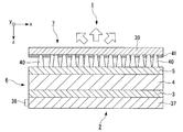
- FIG. 2 is a longitudinal sectional view of the liquid crystal display device of the present embodiment.
- the liquid crystal display device 1 (display device) of this embodiment includes a backlight 2 (light source), a first polarizing plate 3, a liquid crystal panel 4, and a second polarizing plate 5.
- a liquid crystal display body 6 (display body) having a viewing angle and a viewing angle widening film 7 (viewing angle widening member, light diffusion member).
- the light emitted from the backlight 2 is modulated by the liquid crystal panel 4, and a predetermined image, character, or the like is displayed by the modulated light. Further, when the light emitted from the liquid crystal panel 4 passes through the viewing angle widening film 7, the angle distribution of the emitted light becomes wider than before entering the viewing angle widening film 7, and the light is widened. Is injected from. Thereby, the observer can visually recognize the display with a wide viewing angle.
- FIG. 3 is a longitudinal sectional view of the liquid crystal panel 4.
- the liquid crystal panel 4 includes a TFT substrate 9 as a switching element substrate, a color filter substrate 10 disposed so as to face the TFT substrate 9, and the TFT substrate 9 and the color filter substrate 10. And a sandwiched liquid crystal layer 11.
- the liquid crystal layer 11 is surrounded by a TFT substrate 9, a color filter substrate 10, and a frame-shaped seal member (not shown) that bonds the TFT substrate 9 and the color filter substrate 10 at a predetermined interval. It is enclosed in the space.
- the TFT substrate 9 has a plurality of pixels (not shown) as a minimum unit area for display arranged in a matrix.
- a plurality of source bus lines (not shown) are formed on the TFT substrate 9 so as to extend in parallel with each other.
- a plurality of gate bus lines (not shown) are formed to extend in parallel to each other and to be orthogonal to the plurality of source bus lines. Therefore, on the TFT substrate 9, a plurality of source bus lines and a plurality of gate bus lines are formed in a lattice pattern, and a rectangular region partitioned by adjacent source bus lines and adjacent gate bus lines is one.
- the source bus line is connected to the source electrode of the TFT described later, and the gate bus line is connected to the gate electrode of the TFT.
- a TFT 19 having a semiconductor layer 15, a gate electrode 16, a source electrode 17, a drain electrode 18, and the like is formed on the surface of the transparent substrate 14 constituting the TFT substrate 9 on the liquid crystal layer 11 side.
- the transparent substrate 14 for example, a glass substrate can be used.
- a semiconductor layer 15 is formed.
- a gate insulating film 20 is formed on the transparent substrate 14 so as to cover the semiconductor layer 15.
- a material of the gate insulating film 20 for example, a silicon oxide film, a silicon nitride film, or a laminated film thereof is used.
- a gate electrode 16 is formed on the gate insulating film 20 so as to face the semiconductor layer 15.
- a laminated film of W (tungsten) / TaN (tantalum nitride), Mo (molybdenum), Ti (titanium), Al (aluminum), or the like is used.
- a first interlayer insulating film 21 is formed on the gate insulating film 20 so as to cover the gate electrode 16.
- a material of the first interlayer insulating film 21 for example, a silicon oxide film, a silicon nitride film, or a laminated film thereof is used.
- a source electrode 17 and a drain electrode 18 are formed on the first interlayer insulating film 21.
- the source electrode 17 is connected to the source region of the semiconductor layer 15 through a contact hole 22 that penetrates the first interlayer insulating film 21 and the gate insulating film 20.
- the drain electrode 18 is connected to the drain region of the semiconductor layer 15 through a contact hole 23 that penetrates the first interlayer insulating film 21 and the gate insulating film 20.
- a pixel electrode 25 is formed on the second interlayer insulating film 24.
- the pixel electrode 25 is connected to the drain electrode 18 through a contact hole 26 that penetrates the second interlayer insulating film 24. Therefore, the pixel electrode 25 is connected to the drain region of the semiconductor layer 15 using the drain electrode 18 as a relay electrode.
- a transparent conductive material such as ITO (Indium Tin Oxide, Indium Tin Oxide) or IZO (Indium Zinc Oxide, Indium Zinc Oxide) is used.
- An alignment film 27 is formed on the entire surface of the second interlayer insulating film 24 so as to cover the pixel electrode 25.
- This alignment film 27 has an alignment regulating force for vertically aligning liquid crystal molecules constituting the liquid crystal layer 11.
- the form of the TFT may be the bottom gate TFT shown in FIG. 3 or the top gate TFT.
- a black matrix 30, a color filter 31, a planarizing layer 32, a counter electrode 33, and an alignment film 34 are sequentially formed on the surface of the transparent substrate 29 constituting the color filter substrate 10 on the liquid crystal layer 11 side.
- the black matrix 30 has a function of blocking light transmission in the inter-pixel region, and is a photo in which metal such as a multilayer film of Cr (chromium) or Cr / Cr oxide, or carbon particles is dispersed in a photosensitive resin. It is made of resist.
- the color filter 31 includes dyes of red (R), green (G), and blue (B), and one pixel electrode 25 on the TFT substrate 9 is any one of R, G, and B. Two color filters 31 are arranged to face each other.
- the backlight 2 includes a light source 36 such as a light emitting diode and a cold cathode tube, and a light guide plate 37 that emits light toward the liquid crystal panel 4 using internal reflection of light emitted from the light source 36. ,have.
- the backlight 2 may be an edge light type in which the light source is disposed on the end face of the light guide, or may be a direct type in which the light source is disposed directly under the light guide.
- the base material 39 examples include transparent resin base materials such as triacetyl cellulose (TAC) film, polyethylene terephthalate (PET), polycarbonate (PC), polyethylene naphthalate (PEN), and polyethersulfone (PES) film.
- TAC triacetyl cellulose
- PET polyethylene terephthalate
- PC polycarbonate
- PEN polyethylene naphthalate
- PES polyethersulfone
- the base material 39 serves as a base when a material for the black layer 41 and the light diffusion portion 40 is applied later in the manufacturing process described later.
- the base material 39 has heat resistance and mechanical strength in a heat treatment step during the manufacturing process. It is necessary to prepare. Therefore, as the base material 39, a glass base material or the like may be used in addition to the resin base material. However, it is preferable that the thickness of the base material 39 is as thin as possible without impairing heat resistance and mechanical strength.
- the total light transmittance of the substrate 39 is preferably 90% or more in accordance with JIS K7361-1. When the total light transmittance is 90% or more, sufficient transparency can be obtained.
- a transparent resin substrate having a thickness of 100 ⁇ m is used as an example.
- the light diffusion part 40 is a part that contributes to the transmission of light in the viewing angle widening film 7. That is, the light incident on the light diffusing unit 40 is guided and emitted while being totally confined inside the light diffusing unit 40 while being totally reflected by the tapered side surface 40 c of the light diffusing unit 40.
- the plurality of light diffusion portions 40 are randomly arranged as viewed from the normal direction of the main surface of the base material 39.
- the x axis is defined as the horizontal direction of the screen of the liquid crystal panel 4
- the y axis is defined as the vertical direction of the screen of the liquid crystal panel 4
- the z axis is defined as the thickness direction of the liquid crystal display device 1.
- the refractive index of the base material 39 and the refractive index of the light diffusing portion 40 are substantially equal. The reason is that, for example, if the refractive index of the base material 39 and the refractive index of the light diffusing unit 40 are greatly different, the light diffusing unit is used when the light incident from the light incident end surface 40b is emitted from the light diffusing unit 40. This is because unnecessary light refraction or reflection occurs at the interface between the substrate 40 and the base material 39, which may cause problems such as failure to obtain a desired viewing angle and reduction in the amount of emitted light.
- the viewing angle widening film 7 is arranged so that the base material 39 faces the viewing side, so that the smaller one of the two opposing surfaces of the truncated cone-shaped light diffusing portion 40.
- the surface having the larger area becomes the light incident end surface 40b.
- the inclination angle of the side surface 40c of the light diffusing portion 40 (angle formed by the light emission end surface 40a and the side surface 40c) is about 80 ° as an example.
- the inclination angle of the side surface 40c of the light diffusion portion 40 is not particularly limited as long as it is an angle that can sufficiently diffuse incident light when exiting from the viewing angle widening film 7.
- the incident point of the parallel incident light VR on the side surface 40c is a point Q and the intersection of the perpendicular passing through the point Q and the light emitting end surface 40a among the perpendiculars to the light emitting end surface 40a is a point R, it can be expressed by an angle QPR. it can.
- the value of the angle PQR is (90 ⁇ ) °
- the inclination angle ⁇ of the side surface 40c of the light diffusing unit 40 is the same as the incident angle ⁇ ′ of the incident light VR at the point Q. Therefore, the inclination angle ⁇ of the side surface 40c of the light diffusion portion 40 is formed at an angle exceeding the critical angle.
- the side surface 40c of the light diffusion portion 40 is the same as the transparent acrylic resin. It becomes an interface with air.
- the difference in refractive index between the inside and the outside of the light diffusing unit 40 is that any low refractive index material exists outside. The maximum is when air is present. Therefore, from Snell's law, in the configuration of the present embodiment, the critical angle is the smallest, and the incident angle range in which light is totally reflected by the side surface 40c of the light diffusing unit 40 is the widest. As a result, light loss is further suppressed, and high luminance can be obtained.
- incident light incident at an angle exceeding the critical angle is totally reflected by the side surface 40c, passes through the light diffusion portion 40, and is emitted to the observer side.
- incident light that passes through the light diffusing unit 40 without entering the side surface 40c is emitted as it is to the viewer side.
- incident light incident at an angle equal to or smaller than the critical angle is not totally reflected, but is transmitted through the side surface 40 c of the light diffusing unit 40.
- the black layer 41 is provided in a region other than the region where the light diffusion portion 40 is formed, the light transmitted through the side surface 40 c of the light diffusion portion 40 is absorbed by the black layer 41. Therefore, there is no blurring of display and no reduction in contrast.
- the amount of light transmitted through the side surface 40c of the light diffusing unit 40 increases, a light amount loss occurs, and an image with high luminance cannot be obtained. Therefore, in the liquid crystal display device 1 of the present embodiment, it is preferable to use a backlight that emits light at an angle that does not enter the side surface 40c of the light diffusing portion 40 at a critical angle or less, that is, a so-called directional backlight. .
- FIG. 6 The outline of the manufacturing process of the liquid crystal display 6 will be described first. First, the TFT substrate 9 and the color filter substrate 10 are respectively produced. Thereafter, the surface of the TFT substrate 9 on which the TFT 19 is formed and the surface of the color filter substrate 10 on which the color filter 31 is formed are arranged to face each other, and the TFT substrate 9 and the color filter substrate 10 are sealed. Paste through. Thereafter, liquid crystal is injected into a space surrounded by the TFT substrate 9, the color filter substrate 10, and the seal member.
- a triacetyl cellulose base material 39 having a 10 cm square and a thickness of 100 ⁇ m is prepared, and carbon is contained as a black layer material on one surface of the base material 39 by using a spin coating method.
- the black negative resist thus applied is applied to form a coating film 44 having a thickness of 150 nm (step S1 in FIG. 6).
- the base material 39 on which the coating film 44 is formed is placed on a hot plate, and the coating film is pre-baked at a temperature of 90 ° C. Thereby, the solvent in the black negative resist is volatilized.
- step S2 exposure is performed by irradiating the coating film 44 with light through a photomask 45 in which a plurality of light shielding patterns 47 are randomly arranged using an exposure apparatus (step S2 in FIG. 6).
- an exposure apparatus using a mixed line of i-line having a wavelength of 365 nm, h-line having a wavelength of 404 nm, and g-line having a wavelength of 436 nm is used.
- the exposure dose is 100 mJ / cm 2 .
- the transparent negative resist is exposed using the black layer 41 as a mask to form the light diffusing portion 40, so that the position of the light shielding pattern 47 of the photomask 45 is the position where the light diffusing portion 40 is formed.
- the plurality of light shielding patterns 47 are all circular patterns having a diameter of 20 ⁇ m and are randomly arranged. Therefore, although the interval (pitch) between the adjacent light shielding patterns 47 is not constant, the average interval obtained by averaging the intervals between the plurality of light shielding patterns 47 is 25 ⁇ m. It is desirable that the average interval of the light shielding patterns 47 is smaller than the interval (pitch) of the pixels of the liquid crystal panel 4. As a result, at least one light diffusing portion 40 is formed in the pixel, so that a wide viewing angle can be achieved when combined with a liquid crystal panel having a small pixel pitch used for mobile devices, for example.
- a plurality of types of position data A, B, and C created in the previous step are randomly assigned to m ⁇ n areas.
- each position data A, B, C is assigned to each area 46 so that the position data A, position data B, and position data C appear randomly in 36 areas 46. Therefore, when the photomask 45 is viewed for each area 46, the arrangement of the light shielding pattern 47 in each area 46 is applied to any of the position data A, position data B, and position data C patterns, and all the light shielding in all areas.
- the patterns 47 are not arranged at random. However, when the entire photomask 45 is viewed, the plurality of light shielding patterns 47 are randomly arranged.
- a transparent negative resist made of an acrylic resin is applied to the upper surface of the black layer 41 as a light diffusing portion material to form a coating film 48 having a thickness of 25 ⁇ m (FIG. 7C). 6 step S4).
- the base material 39 on which the coating film 48 is formed is placed on a hot plate, and the coating film 48 is pre-baked at a temperature of 95 ° C. Thereby, the solvent in the transparent negative resist is volatilized.
- a diffusion plate having a haze of about 50 may be disposed on the optical path of the light emitted from the exposure apparatus.
- PEB post-exposure baking
- the coating film 48 made of a transparent negative resist is developed using a dedicated developer, post-baked at 100 ° C., and a plurality of light diffusion portions 40 are formed on one surface of the base material 39 as shown in FIG. 7E. (Step S6 in FIG. 6).
- the viewing angle widening film 7 of the present embodiment is completed through the steps S1 to S6 of FIG.
- the total light transmittance of the viewing angle widening film 7 is preferably 90% or more. When the total light transmittance is 90% or more, sufficient transparency can be obtained, and the optical performance required for the viewing angle widening film can be sufficiently exhibited.
- the total light transmittance is as defined in JIS K7361-1.
- the base material 39 may not be turned upside down, and the exposure can be performed from the base material 39 side. It ’s fine.
- a feeding roller 51 for feeding the base material 39 is provided at one end of the manufacturing apparatus 50, and a winding roller 52 for winding the base material 39 is provided at the other end.
- the base material 39 is configured to move from the delivery roller 51 side toward the take-up roller 52 side.
- a printing device 53, a first drying device 54, a coating device 55, a developing device 56, and a second drying device 57 are sequentially arranged from the delivery roller 51 side to the winding roller 52 side.
- An exposure device 58 is disposed below the substrate 39.
- the printing device 53 is for printing the black layer 41 on the base material 39.
- the first drying device 54 is for drying the black layer 41 formed by printing.
- the coating device 55 is for coating a transparent negative resist on the black layer 41.
- the developing device 56 is for developing the exposed transparent negative resist with a developer.
- the second drying device 57 is for drying the base material 39 on which the light diffusion portion 40 made of a developed transparent resist is formed. Thereafter, the base material 39 on which the light diffusion portion 40 is formed may be bonded to the second polarizing plate 5 so that the viewing angle widening film 7 is integrated with the polarizing plate.
- the exposure device 58 is for exposing the coating film 48 of the transparent negative resist from the base material 39 side.
- FIGS. 10A and 10B are views showing only the exposure device 58 in the manufacturing apparatus 50.
- the exposure apparatus 58 includes a plurality of light sources 59, and the diffused light F such as the intensity of the diffused light F from each light source 59 gradually decreases as the base material 39 advances. The strength of the may vary.
- the exposure device 58 may gradually change the emission angle of the diffused light F from each light source 59 as the base material 39 advances. By using such an exposure apparatus 58, the inclination angle of the side surface 40c of the light diffusing unit 40 can be controlled to a desired angle.
- the liquid resist is applied at the time of forming the black layer 41 and the light diffusion layer 40.
- a film-like resist is applied to one surface of the substrate 39. Also good.
- the viewing angle widening effect of the viewing angle widening film 7 of the present embodiment will be described with reference to FIGS. 11A and 11B.
- the light L1 incident substantially perpendicular to the light incident end face 40b near the center of the light diffusion portion 40 is The light diffuser 40 travels straight through as it is without being totally reflected by the side surface 40c of the light diffuser 40.
- the light L2 incident substantially perpendicular to the light incident end surface 40b at the peripheral edge of the light diffusing portion 40 is incident on the side surface 40c of the light diffusing portion at an incident angle larger than the critical angle.
- Total reflection is performed on the side surface 40c. Thereafter, the totally reflected light is further refracted by the light exit end face 40a of the light diffusing portion 40, and is emitted in a direction that forms a large angle with respect to the normal direction of the light exit end face 40a.
- the light L3 incident obliquely with respect to the light incident end face 40b of the light diffusing unit 40 is incident on the side surface 40c of the light diffusing unit 40 at an incident angle smaller than the critical angle. It is transmitted and absorbed by the light absorption layer 41.
- the light L1 and L2 incident on the viewing angle widening film 7 substantially perpendicularly to the viewing angle widening film 7 has a wider angular distribution than that before entering the viewing angle widening film 7, as shown in FIG. Injected from the corner enlargement film 7. Therefore, even if the observer inclines the line of sight from the front direction (normal direction) of the liquid crystal display body 6, a good display can be visually recognized.
- the planar shape of the light diffusing unit 40 is circular, the angular distribution spreads in all directions centered on the normal direction of the screen of the liquid crystal display body 6. Therefore, the observer can visually recognize a good display in all directions.
- an interference fringe pattern is visually recognized when the period of each pattern is slightly shifted.
- a viewing angle widening film in which a plurality of light diffusion portions are arranged in a matrix and a liquid crystal panel in which a plurality of pixels are arranged in a matrix are overlapped, a periodic pattern and liquid crystal by the light diffusion portion of the viewing angle widening film Moire may occur between the periodic patterns of the panel pixels and display quality may be reduced.
- the black layer 41 is disposed on the base material 39.
- FIGS. 13, 14A, and 14B The basic configuration of the liquid crystal display device of this embodiment is the same as that of the first embodiment, and the shape of the light diffusion portion of the viewing angle widening film is different from that of the first embodiment. Therefore, in this embodiment, description of the basic composition of a liquid crystal display device is abbreviate
- FIG. 13 is a longitudinal sectional view showing the liquid crystal display device of this embodiment.
- FIG. 14A is a longitudinal sectional view showing the viewing angle widening film of this embodiment, and FIG.
- the plurality of light diffusing sections 40 are all the same shape.
- the light emitting end face 63a has the same size in the plurality of light diffusion portions 63, but the inclination angle of the side face 63c.
- the side surfaces 63c of the plurality of light diffusion portions 63 have a plurality of types of inclination angles.
- the inclination angle of the side surface 63c is different among the plurality of light diffusion portions 63, the dimensions of the light incident end surface 63b are also different.
- the photomasks 64 used when forming the black layer 41 all have the same size light-shielding pattern 47, which is the same as in the first embodiment.
- the black layer 41 using this photomask 64 when exposing the transparent negative resist, by changing the diffusion angle of the diffused light depending on the location, a plurality of light diffusing portions having different inclination angles of the side surface 63c 63 can be formed.
- Other configurations are the same as those of the first embodiment.
- liquid crystal display device 61 of the present embodiment the same effects as those of the first embodiment that moire does not occur and display quality can be maintained can be obtained.
- the light incident on the light diffusing portion is totally reflected on the side surface of the light diffusing portion, and is emitted from the light diffusing portion with a wider angular distribution than before the incident. Therefore, the angular distribution of the light emitted from the light diffusing unit depends on the distribution of the inclination angle of the side surface of the light diffusing unit. Therefore, as in the first embodiment, if the inclination angle of the side surface 40c of the light diffusing unit 40 is constant, the luminance is high at a specific light emission angle, and a bright display is visible at a specific observation angle. On the other hand, when the display device is observed while changing the angle, display unevenness may be observed depending on the observation angle.
- the inclination angle of the side surface 63c of the light diffusing unit 63 is plural, it is preferable that the luminance changes gently. However, it is possible to obtain the effect of improving the viewing angle characteristics only by setting the inclination angles of at least some of the light diffusion portions to be different from those of other light diffusion portions and setting two types of inclination angles.
- the plurality of light diffusing parts have the same shape.
- the plurality of light diffusing portions have the same light exit end face dimensions and different side surface inclination angles.
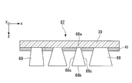
- the viewing angle widening film 67 of the present embodiment as shown in FIGS. 15 and 16A, in the plurality of light diffusing portions 68, the dimensions of the light emission end face 68a (dimensions of the openings of the black layer 41). And the inclination angle of the side surface 68c is also different.
- the light emission end faces 68a of the plurality of light diffusion portions 68 have a plurality of types of dimensions
- the side surfaces 68c of the plurality of light diffusion portions 68 have a plurality of types of inclination angles. is doing.
- the inclination angle of the side surface 68c differs among the plurality of light diffusion portions 68
- the dimensions of the light incident end surface 68b also differ.
- Other configurations are the same as those of the first embodiment.
- the photomask 69 used in forming the black layer 41 has a plurality of light-shielding patterns 70 having different dimensions and a diameter in the range of 10 to 25 ⁇ m.
- the black layer 41 is formed using the photomask 69, the black layer 41 having a plurality of openings with different dimensions is obtained.
- FIG. 17A when the black layer 41 is used as a mask and the coating film 48 made of a transparent negative resist is exposed from the side of the base material 39, the black layer 41 as shown by the symbol A in FIG. 17A.
- the shape of the light exit end face 68a of the light diffusing portion 68 is circular.
- the shape of the light exit end face 68a of the light diffusing portion 68 may be a polygon or may be an ellipse like the light diffusing portion 68A.
- the light diffusing portion 68 may be connected to the light emitting end faces 68a of the adjacent light diffusing portions 68 like the light diffusing portion 68B.
- the light diffusion portion 68 may be partially missing like the light diffusion portion 68C.
- the same effects as those of the first and second embodiments can be obtained, such that moire does not occur and display quality can be maintained.
- the same effect as that of the second embodiment can be obtained in which the luminance changes smoothly according to the observation angle and the viewing angle characteristics can be improved.
- the ratio of the light diffusion portion 68 to the entire viewing angle widening film 67 can be increased by filling a gap between the large light diffusion portions 68 with the small light diffusion portion 68.
- the utilization efficiency of the light from a backlight can be improved and front brightness can be raised.
- FIGS. 19 and 20 The basic configuration of the liquid crystal display device of this embodiment is the same as that of the first embodiment, and the shape of the light diffusion portion of the viewing angle widening film is different from that of the first embodiment. Therefore, in this embodiment, description of the basic composition of a liquid crystal display device is abbreviate
- FIG. 19 is a longitudinal sectional view showing the liquid crystal display device of the present embodiment.
- FIG. 20 is a longitudinal sectional view showing the viewing angle widening film of this embodiment.
- symbol is attached
- the side surface of the light diffusing portion has a constant inclination angle.
- the side surface 74c of each light diffusing portion 74 is gently convex from the light emitting end surface 74a to the light incident end surface 74b. It is curved and the angle of inclination varies from place to place. That is, the inclination angle of the side surface 74c of each light diffusion portion 74 continuously changes from the light exit end surface 74a to the light incident end surface 74b.
- Other configurations are the same as those of the first embodiment.
- liquid crystal display device 72 of the present embodiment the same effects as those of the first to third embodiments can be obtained such that moire does not occur and display quality can be maintained.
- the side surfaces have a plurality of types of inclination angles throughout the plurality of light diffusion portions.
- the viewing angle widening film 73 of the present embodiment since the inclination angle is different depending on the location of the side surface 74c in each light diffusion portion 74, compared with the case where the side surface inclination angle is constant. The light reflection angle distribution is widened. Thereby, the luminance changes gently according to the observation angle, and the viewing angle characteristics can be improved.
- FIG. 21 is a longitudinal sectional view showing the liquid crystal display device of the present embodiment.
- FIG. 22 is a plan view showing the viewing angle widening film of this embodiment. 21 and 22, the same reference numerals are given to the same components as those used in the first embodiment, and the detailed description thereof will be omitted.
- each light diffusing portion of the light diffusing portion has a substantially truncated cone shape, and the planar shapes of the light incident end surface and the light emitting end surface are both circular.
- each light diffusion portion 78 has an octagonal truncated cone shape as shown in FIG. 21, and the planar shapes of the light incident end face 78b and the light exit end face 78a are as follows. Both are octagonal.
- each light diffusion portion 78 Of the eight sides of the octagon that is the planar shape of each light diffusion portion 78, four sets of two sides that are parallel to each other are a direction parallel to the x axis, a direction parallel to the y axis, They are arranged so as to face a direction that forms an angle of 45 ° with the x-axis (an angle viewed counterclockwise with respect to the positive direction of the x-axis) and a direction that forms an angle of 135 ° with the x-axis.
- Other configurations are the same as those of the first embodiment.
- a photomask having an octagonal light shielding pattern may be used in the step of forming the black layer 41.
- liquid crystal display device 76 of this embodiment the same effects as those of the first to fourth embodiments can be obtained, such that moire does not occur and display quality can be maintained.
- the planar shape of the light diffusing portion is circular, light is diffused in all directions around the normal direction of the liquid crystal display 6 and the field of view is visible in all directions. A corner enlargement effect is exhibited.
- the planar shape of the light diffusing portion 78 is an octagon, and the above four sets of sides are parallel to the x-axis, parallel to the y-axis, x Since the light is directed in a direction that forms an angle of 45 ° with the axis and a direction that forms an angle of 135 ° with the x-axis, the light is concentrated and diffused in the above four directions.
- the planar shape of the light diffusing portion 78 is not limited to an octagon, and other polygons can be adopted. In that case, since light is concentrated and diffused in a specific direction according to the shape of the polygon and the arrangement of the sides, a liquid crystal display device that exhibits an excellent viewing angle expansion effect in a specific viewing direction can be provided.
- FIG. 23 is a longitudinal sectional view showing the liquid crystal display device of this embodiment.
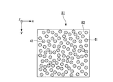
- FIG. 24A is a plan view showing a viewing angle widening film of this embodiment, and
- FIG. 24B is a plan view showing a photomask used for forming a black layer of the viewing angle widening film.
- FIG. 25 is a plan view showing a viewing angle widening film in a liquid crystal display device according to a modification of the present embodiment. 23 to 25, the same reference numerals are given to the same components as those used in the first embodiment, and the detailed description thereof will be omitted.
- the viewing angle widening film 81 includes a region where the light diffusing portion 82 is present and a region where the black layer 41 and the air layer are present according to the first embodiment. It is reversed compared to film. That is, the viewing angle widening film of the first embodiment has a frustoconical light diffusing portion, whereas the viewing angle widening film 81 of the present embodiment is formed on the base material 39 in the frustoconical space. It has a black layer 41 at the contacting part and an air layer at the other part. Therefore, in the black layer 41 of this embodiment, as shown in FIG.
- 24A a plurality of circular black layers 41 are randomly scattered, and the other portions are indefinite shaped light diffusion portions 82.
- 24A shows an example in which the black layer 41 is circular, it may be elliptical or polygonal like the black layer 41A shown in FIG. Moreover, a part of adjacent black layer may be connected like the black layer 41B. Furthermore, as shown by the black layer 41C, one component of the black layer may be missing.
- the shape and dimensions of the black layer 41 may all be substantially the same, or some of the shapes and dimensions may be different.
- the shape of the black layer 41 of the present embodiment is obtained by inverting the shape of the black layer of the first embodiment.
- a photomask 83 used when forming the black layer 41 is used. Is a reverse of the light-shielding pattern and the opening of the photomask used in the first embodiment, and the shaded portion with reference numeral 84 is the light-shielding pattern.
- the light diffusion portion 82 of the present embodiment is provided so as to fill a portion excluding the truncated cone space, and the planar shape of the light diffusion portion 82 is a random indefinite shape.
- the light diffusing portion 82 has a light emission end face 82a and a light incident end face 82b having a larger area than the light emission end face 82a, and the first embodiment is that the side face 82c has a predetermined inclination angle. It is the same as the form.
- liquid crystal display device 80 of the present embodiment the same effects as those of the first to fifth embodiments can be obtained such that moire does not occur and display quality can be maintained.
- the black layer 41 when the black layer 41 is formed, if the size of the opening (the portion serving as the light diffusion portion formation region) becomes fine, the black negative resist present in the opening cannot be completely removed. In some cases, accurate patterning is difficult. In this respect, since the present embodiment is a method of leaving the scattered black layers 41, there is an advantage that the patterning of the black layers 41 is easier than in the first embodiment.
- the seventh embodiment of the present invention will be described below with reference to FIG.
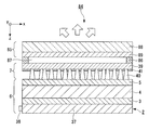
- the basic configuration of the liquid crystal display device of the present embodiment is the same as that of the first embodiment, and is different from the first embodiment in that a touch panel is provided. Therefore, in this embodiment, the description of the basic configuration of the liquid crystal display device is omitted, and only the configuration of the touch panel will be described. Also, in FIG. 26, the same reference numerals are given to the same components as those in FIG. 2 used in the first embodiment, and detailed description thereof will be omitted.
- the configuration from the backlight 2 to the viewing angle widening film 7 is the same as that of the first embodiment.
- the touch panel 85 (information input device) is arrange
- the base material 39 constituting the viewing angle widening film 7 is referred to as a “viewing angle widening film base material”.
- the touch panel 85 is affixed on the viewing angle widening film base material 39 by an adhesive 86 such as a double-sided tape at the periphery of the viewing angle widening film base material 39, and the touch panel 85 and the viewing angle widening film base material 39. A gap corresponding to the thickness of the adhesive 86 is formed between them. That is, an air layer 87 exists between the touch panel 85 and the viewing angle widening film substrate 39.
- the touch panel 85 includes a base material 88 and a position detection electrode 89.
- the base material 88 constituting the touch panel 85 is referred to as a “touch panel base material”.
- a position detection electrode 89 made of a transparent conductive material such as ITO or ATO (Antimony-doped Tin Oxide: tin oxide doped with antimony) is formed on one surface of the touch panel substrate 88 made of glass or the like.
- the position detecting electrode 89 is formed by sputtering of ITO, ATO or the like, and has a uniform sheet resistance of about several hundred to 2 k ⁇ / ⁇ .
- a capacitive touch panel 85 is used.
- minute voltages are applied to four corners of the position detection electrode 89 when the touch panel 85 is viewed in plan.
- the point touched by the finger is grounded via the capacitance of the human body.
- the position detection circuit measures this voltage change as a current change, and detects the ground point, that is, the position touched by the finger from the measured value.
- the touch panel applicable to this embodiment is not restricted to a capacitive system, Arbitrary touch panels, such as a resistive film system, an ultrasonic system, an optical system, are applicable.
- liquid crystal display device 84 of the present embodiment since the viewing angle widening film 7 similar to that of the first embodiment is provided, a liquid crystal display device having excellent viewing angle characteristics and further having an information input function is realized. Can do. For example, when the user touches the touch panel 85 with a finger or a pen while viewing an image with a wide viewing angle, information can be input to the information processing apparatus or the like in an interactive manner.
- the technical scope of the aspect of the present invention is not limited to the above-described embodiment, and various modifications can be made without departing from the spirit of the aspect of the present invention.
- the example of the liquid crystal display device is given as the display body.
- the viewing angle expansion film and the liquid crystal display body do not necessarily need to contact.
- another optical film or an optical component may be inserted between the viewing angle widening film and the liquid crystal display.
- a viewing angle expansion film and a liquid crystal display body may exist in the position which left
- a polarizing plate is unnecessary, so that the viewing angle widening film and the polarizing plate do not come into contact with each other.
- the shape of the light diffusing portion is a truncated cone shape or a polygonal frustum shape.
- the inclination angle of the side surface of the light diffusing portion is not necessarily symmetric about the optical axis.
- the shape of the light diffusing portion is a truncated cone shape or a polygonal frustum shape as in the above embodiment, the inclination angle of the side surface of the light diffusing portion is symmetric about the optical axis. A symmetrical angular distribution is obtained.
- the inclination angle of the side surface of the light diffusing unit may be asymmetric.
- the aspect of the present invention can be used for various display devices such as a liquid crystal display device, an organic electroluminescence display device, and a plasma display.
Landscapes
- Physics & Mathematics (AREA)
- Engineering & Computer Science (AREA)
- General Physics & Mathematics (AREA)
- Optics & Photonics (AREA)
- Nonlinear Science (AREA)
- Manufacturing & Machinery (AREA)
- General Engineering & Computer Science (AREA)
- Theoretical Computer Science (AREA)
- Crystallography & Structural Chemistry (AREA)
- Chemical & Material Sciences (AREA)
- Mathematical Physics (AREA)
- Health & Medical Sciences (AREA)
- Ophthalmology & Optometry (AREA)
- Mechanical Engineering (AREA)
- Human Computer Interaction (AREA)
- Optical Elements Other Than Lenses (AREA)
- Liquid Crystal (AREA)
Abstract
光拡散部材は、光透過性を有する基材と、前記基材の一面に形成された複数の光拡散部と、前記基材の一面のうち前記光拡散部の形成領域以外の領域に形成された光吸収層と、を備え、前記光拡散部が、前記基材側に光射出端面を有するとともに前記基材側と反対側に前記光射出端面の面積よりも大きい面積の光入射端面を有し、前記光拡散部の前記光入射端面から前記光射出端面までの高さが前記光吸収層の層厚よりも大きく、前記複数の光拡散部が、前記基材の一面にランダムに配置されている。
Description
本発明は、光拡散部材およびその製造方法、表示装置に関する。
本願は、2010年10月21日に、日本に出願された特願2010-236513号に基づき優先権を主張し、その内容をここに援用する。
本願は、2010年10月21日に、日本に出願された特願2010-236513号に基づき優先権を主張し、その内容をここに援用する。
携帯電話機等をはじめとする携帯型電子機器、もしくはテレビジョン、パーソナルコンピューター等のディスプレイとして、液晶表示装置が広く用いられている。ところが、一般に液晶表示装置は、正面からの視認性に優れる反面、視野角が狭いことが従来から知られており、視野角を広げるための様々な工夫がなされている。その一つとして、液晶パネル等の表示体から射出される光を拡散させるための部材(以下、光拡散部材と称する)を表示体の視認側に備える構成が考えられる。
例えば下記の特許文献1には、リアプロジェクションスクリーンの一部を構成する光分散フィルムが開示されている。この光分散フィルムは、光透過基板と、光透過基板上に配置された複数の光拡散構造と、を有している。光分散フィルムは、複数の光拡散構造が複数の樹脂構造体からなり、光拡散構造間のキャビティの一部に光吸収性接着剤が充填された構成を有している。
上記の特許文献1に記載の光分散フィルムは、複数の光拡散構造が光透過基板を横切るように延在するリブ状の構造体、もしくは千鳥状に配列された構造体で構成されている。
すなわち、複数の光拡散構造は、規則性を持って配列された複数の構造体で構成されている。そのため、画像を表示した際に光の干渉によるモアレが発生し、表示品位が低下する。
すなわち、複数の光拡散構造は、規則性を持って配列された複数の構造体で構成されている。そのため、画像を表示した際に光の干渉によるモアレが発生し、表示品位が低下する。
本発明の一態様は、画像表示時のモアレを抑制し、視野角を拡大することができる光拡散部材およびその製造方法を提供する。また、上記の光拡散部材を備え、表示品位に優れた表示装置を提供する。
本発明の一態様における光拡散部材は、光透過性を有する基材と、前記基材の一面に形成された複数の光拡散部と、前記基材の一面のうち前記光拡散部の形成領域以外の領域に形成された光吸収層と、を備え、前記光拡散部が、前記基材側に光射出端面を有するとともに前記基材側と反対側に前記光射出端面の面積よりも大きい面積の光入射端面を有し、前記光拡散部の前記光入射端面から前記光射出端面までの高さが前記光吸収層の層厚よりも大きく、前記複数の光拡散部が、前記基材の一面にランダムに配置されている。
本発明の一態様における光拡散部材は、前記複数の光拡散部間の間隙に空気が存在していてもよい。
本発明の一態様における光拡散部材は、前記複数の光拡散部のうち、少なくとも一つの光拡散部の前記光射出端面の寸法が他の光拡散部の前記光射出端面の寸法と異なっていてもよい。
本発明の一態様における光拡散部材は、前記複数の光拡散部のうち、少なくとも一つの光拡散部の側面の傾斜角度が他の光拡散部の側面の傾斜角度と異なっていてもよい。
本発明の一態様における光拡散部材は、前記複数の光拡散部のうち、少なくとも一つの光拡散部の側面の傾斜角度が連続的に変化していてもよい。
本発明の一態様における光拡散部材は、前記基材の一面の法線方向から見た前記光拡散部の平面的な形状が、円形もしくは多角形であってもよい。
本発明の一態様における光拡散部材は、光透過性を有する基材と、前記基材の一面に点在して形成された複数の光吸収層と、前記基材の一面のうち前記光吸収層の形成領域以外の領域に形成された光拡散部と、を備え、前記光拡散部が、前記基材側に光射出端面を有するとともに前記基材側と反対側に前記光射出端面よりも大きい面積の光入射端面を有し、前記光拡散部の前記光入射端面から前記光射出端面までの高さが前記光吸収層の層厚よりも大きく、前記光拡散部が、前記基材の一面の法線方向から見てランダムな形状を有している。
本発明の一態様における光拡散部材は、前記基材の前記一面と反対側の面に、反射防止層、偏光フィルター層、帯電防止層、防眩処理層、防汚処理層のうちの少なくとも一つが設けられていてもよい。
本発明の一態様における光拡散部材の製造方法は、光透過性を有する基材の一面に、少なくとも一つの開口部を有する光吸収層を形成し、前記基材の一面に、前記光吸収層を覆うように光透過性を有するネガ型感光性樹脂層を形成し、前記光吸収層および前記ネガ型感光性樹脂層を形成した前記基材の一面と反対側の面から、前記光吸収層の開口部を通して前記ネガ型感光性樹脂層に対して拡散光を照射し、前記拡散光の照射が終わった前記ネガ型感光性樹脂層を現像し、前記基材側に光射出端面を有するとともに前記基材側と反対側に前記光射出端面の面積よりも大きい面積の光入射端面を有する光拡散部を前記基材の一面に形成することを有する。
本発明の一態様における表示装置は、表示体と、前記表示体の視認側に設けられ、前記表示体から入射される光の角度分布を入射前よりも広げた状態にして光を射出させる視野角拡大部材と、を備え、前記視野角拡大部材が、光透過性を有する基材と、前記基材の一面に形成された複数の光拡散部と、前記基材の一面のうち前記光拡散部の形成領域以外の領域に形成された光吸収層と、を備え、前記光拡散部が、前記基材側に光射出端面を有するとともに前記基材側と反対側に前記光射出端面の面積よりも大きい面積の光入射端面を有し、前記光拡散部の前記光入射端面から前記光射出端面までの高さが前記光吸収層の層厚よりも大きく、前記複数の光拡散部が、前記基材の一面の法線方向から見てランダムに配置されていてもよい。
本発明の一態様における表示装置は、前記表示体が、表示画像を形成する複数の画素を有し、前記光拡散部材の前記複数の光拡散部のうち、隣接する光拡散部間の平均間隔が、前記表示体の前記画素間の間隔よりも小さくてもよい。
本発明の一態様における表示装置は、前記視野角拡大部材の視認側に、情報入力装置が設けられていてもよい。
本発明の一態様における表示装置は、前記表示体が、光源と、前記光源からの光を変調する光変調素子と、を有し、前記光源が指向性を有する光を射出してもよい。
本発明の一態様における表示装置は、前記表示体が液晶表示素子であってもよい。
本発明の態様によれば、画像表示時のモアレを抑制し、視野角を拡大し得る光拡散部材およびその製造方法を提供することができる。また、本発明の態様によれば、上記の光拡散部材を備え、表示品位に優れた表示装置を提供することができる。
〔第1実施形態〕
以下、本発明の第1実施形態について、図1A~図12Bを用いて説明する。
本実施形態では、表示体として透過型の液晶パネルを備えた液晶表示装置の例を挙げて説明する。
なお、以下の全ての図面においては、各構成要素を見やすくするため、構成要素によって寸法の縮尺を異ならせて示すことがある。
以下、本発明の第1実施形態について、図1A~図12Bを用いて説明する。
本実施形態では、表示体として透過型の液晶パネルを備えた液晶表示装置の例を挙げて説明する。
なお、以下の全ての図面においては、各構成要素を見やすくするため、構成要素によって寸法の縮尺を異ならせて示すことがある。
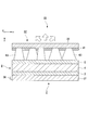
図1Aは本実施形態の液晶表示装置を斜め上方(視認側)から見た斜視図である。図1Bは本実施形態の液晶表示装置を斜め下方(背面側)から見た斜視図である。図2は本実施形態の液晶表示装置の縦断面図である。
本実施形態の液晶表示装置1(表示装置)は、図1A、図1Bおよび図2に示すように、バックライト2(光源)と第1偏光板3と液晶パネル4と第2偏光板5とを有する液晶表示体6(表示体)と、視野角拡大フィルム7(視野角拡大部材、光拡散部材)と、から構成されている。図1Aおよび図2では、液晶パネル4を模式的に1枚の板状に図示しているが、その詳細な構造については後述する。観察者は、視野角拡大フィルム7が配置された図2における液晶表示装置1の上側から表示を見ることになる。よって、以下の説明では、視野角拡大フィルム7が配置された側を視認側と称し、バックライト2が配置された側を背面側と称する。
本実施形態の液晶表示装置1(表示装置)は、図1A、図1Bおよび図2に示すように、バックライト2(光源)と第1偏光板3と液晶パネル4と第2偏光板5とを有する液晶表示体6(表示体)と、視野角拡大フィルム7(視野角拡大部材、光拡散部材)と、から構成されている。図1Aおよび図2では、液晶パネル4を模式的に1枚の板状に図示しているが、その詳細な構造については後述する。観察者は、視野角拡大フィルム7が配置された図2における液晶表示装置1の上側から表示を見ることになる。よって、以下の説明では、視野角拡大フィルム7が配置された側を視認側と称し、バックライト2が配置された側を背面側と称する。
本実施形態の液晶表示装置1においては、バックライト2から射出された光を液晶パネル4で変調し、変調した光によって所定の画像や文字等を表示する。また、液晶パネル4から射出された光が視野角拡大フィルム7を透過すると、射出光の角度分布が視野角拡大フィルム7に入射する前よりも広がった状態となって光が視野角拡大フィルム7から射出される。これにより、観察者は広い視野角をもって表示を視認できる。
以下、液晶パネル4の具体的な構成について説明する。
ここでは、アクティブマトリクス方式の透過型液晶パネルを一例に挙げて説明するが、本発明に適用可能な液晶パネルはアクティブマトリクス方式の透過型液晶パネルに限るものではない。本発明の実施形態に適用可能な液晶パネルは、例えば半透過型(透過・反射兼用型)液晶パネルや反射型液晶パネルであっても良く、更には、各画素がスイッチング用薄膜トランジスタ(Thin Film Transistor、以下、TFTと略記する)を備えていない単純マトリクス方式の液晶パネルであっても良い。
ここでは、アクティブマトリクス方式の透過型液晶パネルを一例に挙げて説明するが、本発明に適用可能な液晶パネルはアクティブマトリクス方式の透過型液晶パネルに限るものではない。本発明の実施形態に適用可能な液晶パネルは、例えば半透過型(透過・反射兼用型)液晶パネルや反射型液晶パネルであっても良く、更には、各画素がスイッチング用薄膜トランジスタ(Thin Film Transistor、以下、TFTと略記する)を備えていない単純マトリクス方式の液晶パネルであっても良い。
図3は、液晶パネル4の縦断面図である。
液晶パネル4は、図3に示すように、スイッチング素子基板としてのTFT基板9と、TFT基板9に対向して配置されたカラーフィルター基板10と、TFT基板9とカラーフィルター基板10との間に挟持された液晶層11と、を有している。液晶層11は、TFT基板9と、カラーフィルター基板10と、TFT基板9とカラーフィルター基板10とを所定の間隔をおいて貼り合わせる枠状のシール部材(図示せず)と、によって囲まれた空間内に封入されている。本実施形態の液晶パネル4は、例えばVA(Vertical Alignment、垂直配向)モードで表示を行うものであり、液晶層11には誘電率異方性が負の垂直配向液晶が用いられる。TFT基板9とカラーフィルター基板10との間には、これら基板間の間隔を一定に保持するための球状のスペーサー12が配置されている。なお、表示モードについては、上記のVAモードに限らず、TN(Twisted Nematic)モード、STN(Super Twisted Nematic)モード、IPS(In-Plane Switching)モード等を用いることができる。
液晶パネル4は、図3に示すように、スイッチング素子基板としてのTFT基板9と、TFT基板9に対向して配置されたカラーフィルター基板10と、TFT基板9とカラーフィルター基板10との間に挟持された液晶層11と、を有している。液晶層11は、TFT基板9と、カラーフィルター基板10と、TFT基板9とカラーフィルター基板10とを所定の間隔をおいて貼り合わせる枠状のシール部材(図示せず)と、によって囲まれた空間内に封入されている。本実施形態の液晶パネル4は、例えばVA(Vertical Alignment、垂直配向)モードで表示を行うものであり、液晶層11には誘電率異方性が負の垂直配向液晶が用いられる。TFT基板9とカラーフィルター基板10との間には、これら基板間の間隔を一定に保持するための球状のスペーサー12が配置されている。なお、表示モードについては、上記のVAモードに限らず、TN(Twisted Nematic)モード、STN(Super Twisted Nematic)モード、IPS(In-Plane Switching)モード等を用いることができる。
TFT基板9には、表示の最小単位領域である画素(図示せず)がマトリクス状に複数配置されている。TFT基板9には、複数のソースバスライン(図示せず)が、互いに平行に延在するように形成される。さらに、複数のゲートバスライン(図示せず)が、互いに平行に延在し、かつ、複数のソースバスラインと直交するように形成されている。したがって、TFT基板9上には、複数のソースバスラインと複数のゲートバスラインとが格子状に形成され、隣接するソースバスラインと隣接するゲートバスラインとによって区画された矩形状の領域が一つの画素となる。ソースバスラインは、後述するTFTのソース電極に接続され、ゲートバスラインは、TFTのゲート電極に接続されている。
TFT基板9を構成する透明基板14の液晶層11側の面に、半導体層15、ゲート電極16、ソース電極17、ドレイン電極18等を有するTFT19が形成されている。透明基板14には、例えばガラス基板を用いることができる。透明基板14上に、例えばCGS(Continuous Grain Silicon:連続粒界シリコン)、LPS(Low-temperature Poly-Silicon:低温多結晶シリコン)、α-Si(Amorphous Silicon:非結晶シリコン)等の半導体材料からなる半導体層15が形成されている。また、透明基板14上に、半導体層15を覆うようにゲート絶縁膜20が形成されている。ゲート絶縁膜20の材料としては、例えばシリコン酸化膜、シリコン窒化膜、もしくはこれらの積層膜等が用いられる。
ゲート絶縁膜20上には、半導体層15と対向するようにゲート電極16が形成されている。ゲート電極16の材料としては、例えばW(タングステン)/TaN(窒化タンタル)の積層膜、Mo(モリブデン)、Ti(チタン)、Al(アルミニウム)等が用いられる。
ゲート絶縁膜20上には、半導体層15と対向するようにゲート電極16が形成されている。ゲート電極16の材料としては、例えばW(タングステン)/TaN(窒化タンタル)の積層膜、Mo(モリブデン)、Ti(チタン)、Al(アルミニウム)等が用いられる。
ゲート絶縁膜20上に、ゲート電極16を覆うように第1層間絶縁膜21が形成されている。第1層間絶縁膜21の材料としては、例えばシリコン酸化膜、シリコン窒化膜、もしくはこれらの積層膜等が用いられる。第1層間絶縁膜21上に、ソース電極17およびドレイン電極18が形成されている。ソース電極17は、第1層間絶縁膜21とゲート絶縁膜20とを貫通するコンタクトホール22を介して半導体層15のソース領域に接続されている。同様に、ドレイン電極18は、第1層間絶縁膜21とゲート絶縁膜20とを貫通するコンタクトホール23を介して半導体層15のドレイン領域に接続されている。ソース電極17およびドレイン電極18の材料としては、上述のゲート電極16と同様の導電性材料が用いられる。第1層間絶縁膜21上に、ソース電極17およびドレイン電極18を覆うように第2層間絶縁膜24が形成されている。第2層間絶縁膜24の材料としては、上述の第1層間絶縁膜21と同様の材料、もしくは有機絶縁性材料が用いられる。
第2層間絶縁膜24上に、画素電極25が形成されている。画素電極25は、第2層間絶縁膜24を貫通するコンタクトホール26を介してドレイン電極18に接続されている。よって、画素電極25は、ドレイン電極18を中継用電極として半導体層15のドレイン領域に接続されている。画素電極25の材料としては、例えばITO(Indium Tin Oxide、インジウム錫酸化物)、IZO(Indium Zinc Oxide、インジウム亜鉛酸化物)等の透明導電性材料が用いられる。この構成により、ゲートバスラインを通じて走査信号が供給され、TFT19がオン状態となったときに、ソースバスラインを通じてソース電極17に供給された画像信号が、半導体層15、ドレイン電極18を経て画素電極25に供給される。また、画素電極25を覆うように第2層間絶縁膜24上の全面に配向膜27が形成されている。この配向膜27は、液晶層11を構成する液晶分子を垂直配向させる配向規制力を有している。なお、TFTの形態としては、図3に示したボトムゲート型TFTであっても良いし、トップゲート型TFTであっても良い。
一方、カラーフィルター基板10を構成する透明基板29の液晶層11側の面には、ブラックマトリクス30、カラーフィルター31、平坦化層32、対向電極33、配向膜34が順次形成されている。ブラックマトリクス30は、画素間領域において光の透過を遮断する機能を有しており、Cr(クロム)やCr/酸化Crの多層膜等の金属、もしくはカーボン粒子を感光性樹脂に分散させたフォトレジストで形成されている。カラーフィルター31には、赤色(R)、緑色(G)、青色(B)の各色の色素が含まれており、TFT基板9上の一つの画素電極25にR,G,Bのいずれか一つのカラーフィルター31が対向して配置されている。平坦化層32は、ブラックマトリクス30およびカラーフィルター31を覆う絶縁膜で構成されており、ブラックマトリクス30およびカラーフィルター31によってできる段差を緩和して平坦化する機能を有している。平坦化層32上には対向電極33が形成されている。対向電極33の材料としては、画素電極25と同様の透明導電性材料が用いられる。また、対向電極33上の全面に、垂直配向規制力を有する配向膜34が形成されている。カラーフィルター31は、R、G、Bの3色以上の多色構成としても良い。
図2に示すように、バックライト2は、発光ダイオード、冷陰極管等の光源36と、光源36から射出された光の内部反射を利用して液晶パネル4に向けて射出させる導光板37と、を有している。バックライト2は、光源が導光体の端面に配置されたエッジライト型でも良く、光源が導光体の直下に配置された直下型でも良い。本実施形態で用いるバックライト2には、光の射出方向を制御して指向性を持たせたバックライト、いわゆる指向性バックライトを用いることが望ましい。後述する視野角拡大フィルム7の光拡散部にコリメートまたは略コリメートした光を入射させるような指向性バックライトを用いることでボヤケを少なくし、さらに光の利用効率を高めることができる。上記の指向性バックライトは、導光板37内に形成する反射パターンの形状や配置等を最適化することで実現できる。また、バックライト2と液晶パネル4との間には、偏光子として機能する第1偏光板3が設けられている。また、液晶パネル4と視野角拡大フィルム7との間には、検光子として機能する第2偏光板5が設けられている。
以下、視野角拡大フィルム7について詳細に説明する。
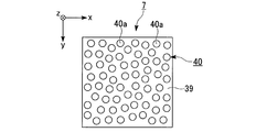
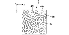
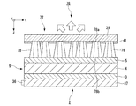
図4Aは、視野角拡大フィルム7の縦断面図であり、図4Bは、視野角拡大フィルム7を視認側から見た平面図であり、図4Cは、視野角拡大フィルム7を背面側から見た平面図である。
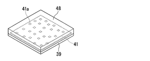
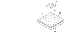
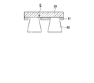
視野角拡大フィルム7は、図4Aに示すように、基材39と、基材39の一面(視認側と反対側の面)に形成された複数の光拡散部40と、基材39の一面に形成された黒色層41(光吸収層)と、から構成されている。この視野角拡大フィルム7は、図2に示すように、光拡散部40が設けられた側を第2偏光板5に向け、基材39の側を視認側に向けた姿勢で第2偏光板5上に配置されている。
図4Aは、視野角拡大フィルム7の縦断面図であり、図4Bは、視野角拡大フィルム7を視認側から見た平面図であり、図4Cは、視野角拡大フィルム7を背面側から見た平面図である。
視野角拡大フィルム7は、図4Aに示すように、基材39と、基材39の一面(視認側と反対側の面)に形成された複数の光拡散部40と、基材39の一面に形成された黒色層41(光吸収層)と、から構成されている。この視野角拡大フィルム7は、図2に示すように、光拡散部40が設けられた側を第2偏光板5に向け、基材39の側を視認側に向けた姿勢で第2偏光板5上に配置されている。
基材39には、例えばトリアセチルセルロース(TAC)フィルム、ポリエチレンテレフタレート(PET)、ポリカーボネート(PC)、ポリエチレンナフタレート(PEN)、ポリエーテルサルホン(PES)フィルム等の透明樹脂製の基材が好ましく用いられる。基材39は、後述する製造プロセスにおいて、後で黒色層41や光拡散部40の材料を塗布する際の下地となるものであり、製造プロセス中の熱処理工程における耐熱性と機械的強度とを備える必要がある。したがって、基材39には、樹脂製の基材の他、ガラス製の基材等を用いても良い。ただし、基材39の厚さは耐熱性や機械的強度を損なわない程度に薄い方が好ましい。その理由は、基材39の厚さが厚くなる程、表示のボヤケが生じる虞があるからである。また、基材39の全光線透過率は、JIS K7361-1の規定で90%以上が好ましい。全光線透過率が90%以上であると、十分な透明性が得られる。本実施形態では、一例として厚さが100μmの透明樹脂製基材を用いる。
光拡散部40は、例えばアクリル樹脂やエポキシ樹脂等の光透過性および感光性を有する有機材料で構成されている。また、光拡散部40の全光線透過率は、JIS K7361-1の規定で90%以上が好ましい。全光線透過率が90%以上であると、十分な透明性が得られる。図4B、および図4Cに示すように、光拡散部40は、水平断面(xy断面)の形状が円形であり、光射出端面となる基材39側の面40aの面積が小さく、光入射端面となる基材39と反対側の面40bの面積が大きく、基材39側から基材39と反対側に向けて水平断面の面積が徐々に大きくなっている。すなわち、光拡散部40は、基材39側から見たとき、いわゆる逆テーパ状の円錐台状の形状を有している。
光拡散部40は、視野角拡大フィルム7において光の透過に寄与する部分である。すなわち、光拡散部40に入射した光は、光拡散部40のテーパ状の側面40cで全反射しつつ、光拡散部40の内部に略閉じこめられた状態で導光し、射出される。複数の光拡散部40は、図4B、図4Cに示すように、基材39の主面の法線方向から見てランダムに配置されている。なお、x軸は液晶パネル4の画面の水平方向、y軸は液晶パネル4の画面の垂直方向、z軸は液晶表示装置1の厚さ方向、と定義する。
黒色層41は、図4Aに示すように、基材39の光拡散部40が形成された側の面のうち、複数の光拡散部40の形成領域以外の領域に形成されている。黒色層41は、一例として、ブラックレジスト等の光吸収性および感光性を有する有機材料で構成されている。このほか、Cr(クロム)やCr/酸化Crの多層膜等の金属膜を用いても良い。黒色層41の層厚は、光拡散部40の光入射端面40bから光射出端面40aまでの高さよりも小さく設定されている。本実施形態の場合、黒色層41の層厚は一例として150nm程度であり、光拡散部40の光入射端面40bから光射出端面40aまでの高さは一例として25μm程度である。したがって、複数の光拡散部40間の間隙は基材39の一面に接する部分には黒色層41が存在し、それ以外の部分には空気が存在している。
なお、基材39の屈折率と光拡散部40の屈折率とは略同等であることが望ましい。その理由は、例えば基材39の屈折率と光拡散部40の屈折率とが大きく異なっていると、光入射端面40bから入射した光が光拡散部40から射出しようとする際に光拡散部40と基材39との界面で不要な光の屈折や反射が生じて、所望の視野角が得られない、射出光の光量が減少する、等の不具合が生じる虞があるからである。
視野角拡大フィルム7は、図2に示したように、基材39が視認側に向くように配置されるため、円錐台状の光拡散部40の2つの対向面のうち、面積の小さい方の面が光射出端面40aとなり、面積の大きい方の面が光入射端面40bとなる。また、光拡散部40の側面40cの傾斜角(光射出端面40aと側面40cとのなす角)は一例として80°程度である。ただし、光拡散部40の側面40cの傾斜角度は、視野角拡大フィルム7から射出する際に入射光を十分に拡散することが可能な角度であれば、特に限定されない。
図5Bに示すように、光拡散部40の側面40cと光射出端面40aとのなす角は、光軸OAと平行または略平行に入射した光を全反射させるように、光拡散部40の側面40cの法線CLに対して臨界角を超える角度θ’(単位は度[°])に設定される。また、光拡散部40の側面40cと光軸OAに直交する光射出端面40aとのなす角度θは、光拡散部40の側面40cが光射出端面40aと交わる点を点P、光軸OAに平行な入射光VRの側面40cへの入射点を点Q、光射出端面40aに対する垂線のうちで点Qを通る垂線と光射出端面40aとの交点を点Rとすると、角QPRで表すことができる。このとき、角PQRの値は(90-θ)°であるから、光拡散部40の側面40cの傾斜角θは点Qにおける入射光VRの入射角θ’と同じ角度となる。したがって、光拡散部40の側面40cの傾斜角θは上記臨界角を超える角度で形成されている。
本実施形態の場合、隣接する光拡散部40間には空気が介在しているため、光拡散部40を例えば透明アクリル樹脂で形成したとすると、光拡散部40の側面40cは透明アクリル樹脂と空気との界面となる。ここで、光拡散部40の周囲を他の低屈折率材料で充填したとしても、光拡散部40の内部と外部との界面の屈折率差は、外部にいかなる低屈折率材料が存在する場合よりも空気が存在する場合が最大となる。したがって、Snellの法則より、本実施形態の構成においては臨界角が最も小さくなり、光拡散部40の側面40cで光が全反射する入射角範囲が最も広くなる。その結果、光の損失がより抑えられ、高い輝度を得ることができる。
図5Aの矢印LBおよびLCに示すように、臨界角を超える角度で入射した入射光は、側面40cで全反射して光拡散部40を透過して観察者側へ射出される。また、図5Aの矢印LAに示すように、側面40cに入射することなく光拡散部40を透過する入射光は、そのまま観察者側へ射出される。一方、図5Aの矢印LDで示すように、臨界角以下の角度で入射した入射光は全反射せず、光拡散部40の側面40cを透過する。本実施形態の場合、光拡散部40の形成領域以外の領域に黒色層41が設けられているので、光拡散部40の側面40cを透過した光は黒色層41で吸収される。そのため、表示のボヤケが生じたり、コントラストが低下したりすることはない。しかしながら、光拡散部40の側面40cを透過する光が増えると、光量のロスが生じ、輝度の高い画像が得られない。そこで、本実施形態の液晶表示装置1においては、光拡散部40の側面40cに臨界角以下で入射しないような角度で光を射出するバックライト、いわゆる指向性を有するバックライトを用いることが好ましい。
次に、上記構成の液晶表示装置1の製造方法について、図6~図10Bを用いて説明する。
以下では、視野角拡大フィルム7の製造工程を中心に説明する。
液晶表示体6の製造工程の概略を先に説明すると、最初に、TFT基板9とカラーフィルター基板10をそれぞれ作製する。その後、TFT基板9のTFT19が形成された側の面とカラーフィルター基板10のカラーフィルター31が形成された側の面とを対向させて配置し、TFT基板9とカラーフィルター基板10とをシール部材を介して貼り合わせる。その後、TFT基板9とカラーフィルター基板10とシール部材とによって囲まれた空間内に液晶を注入する。そして、このようにしてできた液晶パネル4の両面に、光学接着剤等を用いて第1偏光板3、第2偏光板4をそれぞれ貼り合わせる。以上の工程を経て、液晶表示体6が完成する。
なお、TFT基板9やカラーフィルター基板10の製造方法には従来から公知の方法が用いられるため、説明を省略する。
以下では、視野角拡大フィルム7の製造工程を中心に説明する。
液晶表示体6の製造工程の概略を先に説明すると、最初に、TFT基板9とカラーフィルター基板10をそれぞれ作製する。その後、TFT基板9のTFT19が形成された側の面とカラーフィルター基板10のカラーフィルター31が形成された側の面とを対向させて配置し、TFT基板9とカラーフィルター基板10とをシール部材を介して貼り合わせる。その後、TFT基板9とカラーフィルター基板10とシール部材とによって囲まれた空間内に液晶を注入する。そして、このようにしてできた液晶パネル4の両面に、光学接着剤等を用いて第1偏光板3、第2偏光板4をそれぞれ貼り合わせる。以上の工程を経て、液晶表示体6が完成する。
なお、TFT基板9やカラーフィルター基板10の製造方法には従来から公知の方法が用いられるため、説明を省略する。
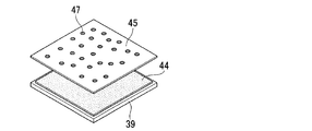
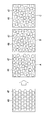
最初に、図7Aに示すように、10cm角で厚さが100μmのトリアセチルセルロースの基材39を準備し、スピンコート法を用いて、この基材39の一面に黒色層材料としてカーボンを含有したブラックネガレジストを塗布し、膜厚150nmの塗膜44を形成する(図6のステップS1)。
次いで、上記の塗膜44を形成した基材39をホットプレート上に載置し、温度90℃で塗膜のプリベークを行う。これにより、ブラックネガレジスト中の溶媒が揮発する。
次いで、上記の塗膜44を形成した基材39をホットプレート上に載置し、温度90℃で塗膜のプリベークを行う。これにより、ブラックネガレジスト中の溶媒が揮発する。
次いで、露光装置を用い、複数の遮光パターン47がランダムに配置されたフォトマスク45を介して塗膜44に光を照射し、露光を行う(図6のステップS2)。このとき、波長365nmのi線、波長404nmのh線、波長436nmのg線の混合線を用いた露光装置を使用する。露光量は100mJ/cm2とする。本実施形態の場合、次工程で黒色層41をマスクとして透明ネガレジストの露光を行い、光拡散部40を形成するため、フォトマスク45の遮光パターン47の位置が光拡散部40の形成位置に対応する。複数の遮光パターン47は全て直径20μmの円形パターンであり、ランダムに配置されている。そのため、隣接する遮光パターン47間の間隔(ピッチ)は一定でないが、複数の遮光パターン47間の間隔を平均した平均間隔は25μmである。遮光パターン47の平均間隔は液晶パネル4の画素の間隔(ピッチ)よりも小さいことが望ましい。これにより、画素内に少なくとも1つの光拡散部40が形成されるので、例えばモバイル機器等に用いる画素ピッチが小さい液晶パネルと組み合わせたときに広視野角化を図ることができる。
ここで、複数の遮光パターン47がランダムに配置されたフォトマスク45を設計する手法の一例について説明する。
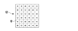
最初に、図8Aに示すように、フォトマスク45の全体を縦m個(例えば6個)、横n個(例えば6個)からなるm×n個(例えば36個)の領域46に分割する。
次に、図8Bに示すように、前の工程で分割した1つの領域46において、遮光パターン47の形状に対応する円を最密充填となるように配置したパターンを作成する(図8Bの左側の図)。次に、ランダム関数を用いて例えば各円の中心座標等、各円の位置の基準となる位置データに揺らぎを持たせ、複数種類(例えばA,B,Cの3種類のパターン)の位置データを作製する(図8Bの右側の3つの図)。
最初に、図8Aに示すように、フォトマスク45の全体を縦m個(例えば6個)、横n個(例えば6個)からなるm×n個(例えば36個)の領域46に分割する。
次に、図8Bに示すように、前の工程で分割した1つの領域46において、遮光パターン47の形状に対応する円を最密充填となるように配置したパターンを作成する(図8Bの左側の図)。次に、ランダム関数を用いて例えば各円の中心座標等、各円の位置の基準となる位置データに揺らぎを持たせ、複数種類(例えばA,B,Cの3種類のパターン)の位置データを作製する(図8Bの右側の3つの図)。
次に、図8Cに示すように、前の工程で作製した複数種類の位置データA,B,Cをm×n個の領域に対してランダムに割り当てる。例えば、位置データA、位置データB、位置データCが36個の領域46にランダムに出現するように各位置データA,B,Cを各領域46に割り当てる。したがって、フォトマスク45を個々の領域46毎に見ると、各領域46の遮光パターン47の配置は位置データA、位置データB、位置データCのいずれかのパターンに当てはまり、全領域で全ての遮光パターン47が全くランダムに配置されている訳ではない。しかしながら、フォトマスク45の全体を見ると、複数の遮光パターン47はランダムに配置されている。
上記のフォトマスク45を用いて露光を行った後、専用の現像液を用いてブラックネガレジストからなる塗膜44の現像を行い、100℃で乾燥し、図7Bに示すように、複数の円形の開口部41aを有する黒色層41を基材39の一面に形成する(図6のステップS3)。円形の開口部41aは次工程の光拡散部40の形成領域に対応する。本実施形態では、ブラックネガレジストを用いたフォトリソグラフィー法によって黒色層41を形成したが、この構成に代えて、本実施形態の遮光パターン47と光透過部とが反転したフォトマスクを用いれば、ポジレジストを用いることもできる。もしくは、蒸着法や印刷法等を用いて黒色層41を形成しても良い。
次いで、図7Cに示すように、スピンコート法を用いて、黒色層41の上面に光拡散部材料としてアクリル樹脂からなる透明ネガレジストを塗布し、膜厚25μmの塗膜48を形成する(図6のステップS4)。
次いで、上記の塗膜48を形成した基材39をホットプレート上に載置し、温度95℃で塗膜48のプリベークを行う。これにより、透明ネガレジスト中の溶媒が揮発する。
次いで、上記の塗膜48を形成した基材39をホットプレート上に載置し、温度95℃で塗膜48のプリベークを行う。これにより、透明ネガレジスト中の溶媒が揮発する。
次いで、図7Dに示すように、基材39を上下反転し、基材39側から黒色層41をマスクとして塗膜48に拡散光Fを照射し、露光を行う(図5のステップS5)。このとき、波長365nmのi線、波長404nmのh線、波長436nmのg線の混合線を用いた露光装置を使用する。露光量は500mJ/cm2とする。また、露光装置から射出された平行光を拡散光Fとして基材に照射する手段としては、例えば露光装置から射出された光の光路上にヘイズ50程度の拡散板を配置すれば良い。
その後、上記の塗膜48を形成した基材39をホットプレート上に載置し、温度95℃で塗膜48のポストエクスポージャーベイク(PEB)を行う。
その後、上記の塗膜48を形成した基材39をホットプレート上に載置し、温度95℃で塗膜48のポストエクスポージャーベイク(PEB)を行う。
次いで、専用の現像液を用いて透明ネガレジストからなる塗膜48の現像を行い、100℃でポストベークし、図7Eに示すように、複数の光拡散部40を基材39の一面に形成する(図6のステップS6)。
以上、図6のステップS1~S6の工程を経て、本実施形態の視野角拡大フィルム7が完成する。視野角拡大フィルム7の全光線透過率は、90%以上が好ましい。全光線透過率が90%以上であると、十分な透明性が得られ、視野角拡大フィルムに求められる光学性能を十分に発揮できる。全光線透過率は、JIS K7361-1の規定によるものである。
以上、図6のステップS1~S6の工程を経て、本実施形態の視野角拡大フィルム7が完成する。視野角拡大フィルム7の全光線透過率は、90%以上が好ましい。全光線透過率が90%以上であると、十分な透明性が得られ、視野角拡大フィルムに求められる光学性能を十分に発揮できる。全光線透過率は、JIS K7361-1の規定によるものである。
なお、基材39を上下反転した上で露光を行うと説明したが、製造装置によっては基材39を上下反転させなくても良く、基材39側から露光が行えるような構成になっていれば良い。
図9は視野角拡大フィルム7の製造装置の一例を示す概略構成図である。
図9に示す製造装置50は、長尺の基材39をロール・トゥー・ロールで搬送し、その間に各種の処理を行うものである。また、この製造装置50は、黒色層41の形成に、上述のフォトマスク45を用いたフォトリソグラフィー法に代えて、印刷法を用いている。
図9に示す製造装置50は、長尺の基材39をロール・トゥー・ロールで搬送し、その間に各種の処理を行うものである。また、この製造装置50は、黒色層41の形成に、上述のフォトマスク45を用いたフォトリソグラフィー法に代えて、印刷法を用いている。
製造装置50の一端に基材39を送り出す送出ローラー51が設けられ、他端には基材39を巻き取る巻取ローラー52が設けられている。基材39は送出ローラー51側から巻取ローラー52側に向けて移動する構成となっている。基材39の上方には、送出ローラー51側から巻取ローラー52側に向けて印刷装置53、第1乾燥装置54、塗布装置55、現像装置56、第2乾燥装置57が順次配置されている。基材39の下方には、露光装置58が配置されている。印刷装置53は、基材39上に黒色層41を印刷するためのものである。第1乾燥装置54は、印刷により形成した黒色層41を乾燥させるためのものである。塗布装置55は、黒色層41上に透明ネガレジストを塗布するためのものである。現像装置56は、露光後の透明ネガレジストを現像液によって現像するためのものである。第2乾燥装置57は、現像後の透明レジストからなる光拡散部40が形成された基材39を乾燥させるためのものである。この後さらに、光拡散部40が形成された基材39を第2偏光板5と貼り合わせ、視野角拡大フィルム7を偏光板と一体化させても良い。
露光装置58は、基材39側から透明ネガレジストの塗膜48の露光を行うためのものである。図10Aおよび図10Bは、製造装置50のうち、露光装置58の部分だけを取り出して示す図である。露光装置58は、図10Aに示すように、複数の光源59を備えており、基材39の進行に伴って、各光源59からの拡散光Fの強度が徐々に弱くなる等、拡散光Fの強度が変化しても良い。あるいは、露光装置58は、図10Bに示すように、基材39の進行に伴って、各光源59からの拡散光Fの射出角度が徐々に変化しても良い。このような露光装置58を用いることにより、光拡散部40の側面40cの傾斜角度を所望の角度に制御することができる。
なお、上記の例では黒色層41や光拡散層40の形成時に液状のレジストを塗布することとしたが、この構成に代えて、フィルム状のレジストを基材39の一面に貼付するようにしても良い。
最後に、完成した視野角拡大フィルム7を、図2に示すように、基材39を視認側に向け、光拡散部40を第2偏光板5に対向させた状態で、光学接着剤等を用いて液晶表示体6に貼付する。
以上の工程により、本実施形態の液晶表示装置1が完成する。
以上の工程により、本実施形態の液晶表示装置1が完成する。
ここで、本実施形態の視野角拡大フィルム7が有する視野角拡大効果について、図11Aおよび11Bを用いて説明する。
図11Aに示すように、液晶表示体6から射出され、視野角拡大フィルム7に入射した光のうち、光拡散部40の中心付近において光入射端面40bに対して略垂直に入射した光L1は、光拡散部40の側面40cで全反射することなく、光拡散部40をそのまま直進して透過する。また、光拡散部40の周縁部において光入射端面40bに対して略垂直に入射した光L2は、臨界角よりも大きい入射角で光拡散部の側面40cに入射するため、光拡散部40の側面40cで全反射する。全反射した光は、その後、光拡散部40の光射出端面40aでさらに屈折し、光射出端面40aの法線方向に対して大きな角度をなす方向に射出される。一方、光拡散部40の光入射端面40bに対して斜めに入射した光L3は、臨界角よりも小さい入射角で光拡散部40の側面40cに入射するため、光拡散部40の側面40cを透過し、光吸収層41で吸収される。
図11Aに示すように、液晶表示体6から射出され、視野角拡大フィルム7に入射した光のうち、光拡散部40の中心付近において光入射端面40bに対して略垂直に入射した光L1は、光拡散部40の側面40cで全反射することなく、光拡散部40をそのまま直進して透過する。また、光拡散部40の周縁部において光入射端面40bに対して略垂直に入射した光L2は、臨界角よりも大きい入射角で光拡散部の側面40cに入射するため、光拡散部40の側面40cで全反射する。全反射した光は、その後、光拡散部40の光射出端面40aでさらに屈折し、光射出端面40aの法線方向に対して大きな角度をなす方向に射出される。一方、光拡散部40の光入射端面40bに対して斜めに入射した光L3は、臨界角よりも小さい入射角で光拡散部40の側面40cに入射するため、光拡散部40の側面40cを透過し、光吸収層41で吸収される。
以上の作用により、図11Bに示すように、視野角拡大フィルム7に対して略垂直に入射した光L1,L2は、視野角拡大フィルム7に入射する前よりも角度分布が広がった状態で視野角拡大フィルム7から射出される。したがって、観察者が液晶表示体6の正面方向(法線方向)から視線を傾けていっても良好な表示を視認することができる。特に本実施形態の場合、光拡散部40の平面形状が円形であるため、液晶表示体6の画面の法線方向を中心とした全ての方位に角度分布が広がる。そのため、観察者は全ての方位で良好な表示を視認できる。すなわち、この視野角拡大フィルム7の使用によって液晶表示体6の視野角を拡大することができる。一方、視野角拡大フィルム7に対して斜めに入射した光L3は、液晶パネル4を斜めに透過した光であり、所望のリタデーションと異なる光、いわゆる表示のコントラストを低下させる要因となる光である。本実施形態の視野角拡大フィルム7は、このような光を光吸収層41でカットすることで表示のコントラストを高めることができる。
一般に、ストライプや格子等のような規則性のあるパターン同士を重ね合わせた場合、各パターンの周期が僅かにずれると、干渉縞模様(モアレ)が視認されることが知られている。例えば複数の光拡散部がマトリクス状に配列された視野角拡大フィルムと複数の画素がマトリクス状に配列された液晶パネルとを重ね合わせたとすると、視野角拡大フィルムの光拡散部による周期パターンと液晶パネルの画素による周期パターンとの間でモアレが発生し、表示品位を低下させる虞がある。これに対して、本実施形態の液晶表示装置1によれば、複数の光拡散部40が平面的にランダムに配置されているため、液晶パネル4の画素の規則的配列との間で干渉によるモアレが生じることがなく、表示品位を維持することができる。
また、光拡散部40を形成する工程において、仮に透明ネガレジストからなる塗膜48側からフォトマスクを介して光を照射したとすると、微小サイズの黒色層41を形成した基材39とフォトマスクとのアライメント調整が非常に困難であり、ずれが生じることが避けられない。その結果、図12Bに示すように、光拡散部40と黒色層41との間に隙間Sができ、隙間Sから光が漏れることによってコントラストが低下する虞がある。
これに対して、本実施形態の場合、図12Aに示すように、黒色層41をマスクとして基材39の背面側から光を照射しているため、光拡散部40が黒色層41の開口部41aの位置に自己整合(セルフアライン)した状態で形成される。その結果、光拡散部40と黒色層41とが密着した状態となってこれらの間に隙間ができず、コントラストを確実に維持することができる。
また、黒色層41を基材39に設けない場合、視野角拡大フィルム7に入射する外光も散乱する。外光散乱が発生すると明所での視認性が低下するのに加え、黒表示時に黒色が白っぽく見える「黒浮き」が発生してコントラストが低下してしまい、好適な画像の観察を行うことができない。これらを防止するために、黒色層41を基材39に配置する。
これに対して、本実施形態の場合、図12Aに示すように、黒色層41をマスクとして基材39の背面側から光を照射しているため、光拡散部40が黒色層41の開口部41aの位置に自己整合(セルフアライン)した状態で形成される。その結果、光拡散部40と黒色層41とが密着した状態となってこれらの間に隙間ができず、コントラストを確実に維持することができる。
また、黒色層41を基材39に設けない場合、視野角拡大フィルム7に入射する外光も散乱する。外光散乱が発生すると明所での視認性が低下するのに加え、黒表示時に黒色が白っぽく見える「黒浮き」が発生してコントラストが低下してしまい、好適な画像の観察を行うことができない。これらを防止するために、黒色層41を基材39に配置する。
[第2実施形態]
以下、本発明の第2実施形態について、図13、図14Aおよび図14Bを用いて説明する。
本実施形態の液晶表示装置の基本構成は第1実施形態と同一であり、視野角拡大フィルムの光拡散部の形状が第1実施形態と異なる。したがって、本実施形態では、液晶表示装置の基本構成の説明は省略し、視野角拡大フィルムについてのみ説明する。
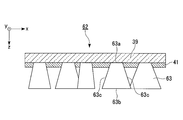
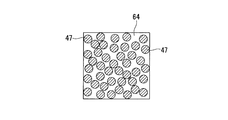
図13は本実施形態の液晶表示装置を示す縦断面図である。図14Aは本実施形態の視野角拡大フィルムを示す縦断面図であり、図14Bは視野角拡大フィルムの製造に用いるフォトマスクを示す平面図である。
また、図13、図14A、および図14Bにおいて、第1実施形態で用いた図面と共通の構成要素には同一の符号を付し、その詳細な説明は省略する。
以下、本発明の第2実施形態について、図13、図14Aおよび図14Bを用いて説明する。
本実施形態の液晶表示装置の基本構成は第1実施形態と同一であり、視野角拡大フィルムの光拡散部の形状が第1実施形態と異なる。したがって、本実施形態では、液晶表示装置の基本構成の説明は省略し、視野角拡大フィルムについてのみ説明する。
図13は本実施形態の液晶表示装置を示す縦断面図である。図14Aは本実施形態の視野角拡大フィルムを示す縦断面図であり、図14Bは視野角拡大フィルムの製造に用いるフォトマスクを示す平面図である。
また、図13、図14A、および図14Bにおいて、第1実施形態で用いた図面と共通の構成要素には同一の符号を付し、その詳細な説明は省略する。
第1実施形態では、複数の光拡散部40は全て同一の形状である。これに対して、本実施形態の視野角拡大フィルム62では、図13および図14Aに示すように、複数の光拡散部63において光射出端面63aの寸法は同一であるが、側面63cの傾斜角度が異なっている。すなわち、複数の光拡散部63全体では、複数の光拡散部63の側面63cが複数種類の傾斜角度を有していることになる。また、複数の光拡散部63で側面63cの傾斜角度が異なることに伴って、光入射端面63bの寸法も異なっている。
図14Bに示すように、黒色層41の形成時に用いるフォトマスク64は、全て同一寸法の遮光パターン47を有しており、第1実施形態と同様である。このフォトマスク64を用いて黒色層41を形成した後、透明ネガレジストの露光を行う際に、拡散光の拡散角度を場所によって変化させることによって、側面63cの傾斜角度が異なる複数の光拡散部63を形成することができる。その他の構成は第1の実施形態と同様である。
本実施形態の液晶表示装置61においても、モアレが生じることがなく、表示品位を維持できる、といった第1実施形態と同様の効果が得られる。
第1実施形態で述べたように、光拡散部に入射した光は、光拡散部の側面で全反射し、入射前よりも角度分布が広がった状態で光拡散部から射出される。よって、光拡散部から射出される光の角度分布は、光拡散部の側面の傾斜角度の分布に依存することになる。そのため、第1実施形態のように、光拡散部40の側面40cの傾斜角度が一定であったとすると、特定の光射出角度では輝度が高くなり、特定の観察角度では明るい表示が視認できる。その反面、角度を変えて表示装置を観察した際に、観察角度によっては表示ムラが観察される虞がある。
これに対して、本実施形態の構成によれば、複数の光拡散部63の側面63cの傾斜角度が互いに異なっているので、光の全反射角度の範囲を、側面63cの傾斜角度が異なる複数の光拡散部63の間で補間し合って広げることができる。その結果、角度を変えて液晶表示装置61を観察した際に観察角度に応じて輝度がなだらかに変化し、視野角特性を向上することができる。
なお、本実施形態では、光拡散部63の側面63cの傾斜角度を複数種類としたため、輝度がなだらかに変化して好ましい。ただし、少なくとも一部の光拡散部の傾斜角度を他の光拡散部と異ならせ、2種類の傾斜角度を設定するだけでも、視野角特性の向上効果は得られる。
[第3実施形態]
以下、本発明の第3実施形態について、図15~図18Cを用いて説明する。
本実施形態の液晶表示装置の基本構成は第1、第2実施形態と同一であり、視野角拡大フィルムの光拡散部の形状が第1、第2実施形態と異なる。したがって、本実施形態では、液晶表示装置の基本構成の説明は省略し、視野角拡大フィルムについてのみ説明する。
図15は本実施形態の液晶表示装置を示す縦断面図である。図16Aは本実施形態の視野角拡大フィルムを示す縦断面図であり、図16Bは視野角拡大フィルムの製造に用いるフォトマスクを示す平面図である。図17Aおよび図17Bは本実施形態の視野角拡大フィルムの製造方法を説明するための図である。図18Aは、本実施形態の変形例の液晶表示装置における視野角拡大フィルムを示す断面図である。図18Bおよび図18Cは、本実施形態の変形例の液晶表示装置における視野角拡大フィルムを示す平面図である。
また、図15~図18Cにおいて、第1、第2実施形態で用いた図面と共通の構成要素には同一の符号を付し、その詳細な説明は省略する。
以下、本発明の第3実施形態について、図15~図18Cを用いて説明する。
本実施形態の液晶表示装置の基本構成は第1、第2実施形態と同一であり、視野角拡大フィルムの光拡散部の形状が第1、第2実施形態と異なる。したがって、本実施形態では、液晶表示装置の基本構成の説明は省略し、視野角拡大フィルムについてのみ説明する。
図15は本実施形態の液晶表示装置を示す縦断面図である。図16Aは本実施形態の視野角拡大フィルムを示す縦断面図であり、図16Bは視野角拡大フィルムの製造に用いるフォトマスクを示す平面図である。図17Aおよび図17Bは本実施形態の視野角拡大フィルムの製造方法を説明するための図である。図18Aは、本実施形態の変形例の液晶表示装置における視野角拡大フィルムを示す断面図である。図18Bおよび図18Cは、本実施形態の変形例の液晶表示装置における視野角拡大フィルムを示す平面図である。
また、図15~図18Cにおいて、第1、第2実施形態で用いた図面と共通の構成要素には同一の符号を付し、その詳細な説明は省略する。
第1実施形態では、複数の光拡散部は全て同一の形状である。第2の実施形態では、複数の光拡散部は、光射出端面の寸法は同一であり、側面の傾斜角度が異なっている。これに対して、本実施形態の視野角拡大フィルム67では、図15および図16Aに示すように、複数の光拡散部68において、光射出端面68aの寸法(黒色層41の開口部の寸法)が異なり、側面68cの傾斜角度も異なっている。すなわち、複数の光拡散部68全体を見ると、複数の光拡散部68の光射出端面68aが複数種類の寸法を有し、複数の光拡散部68の側面68cが複数種類の傾斜角度を有している。また、複数の光拡散部68で側面68cの傾斜角度が異なることに伴って、光入射端面68bの寸法も異なっている。その他の構成は第1の実施形態と同様である。
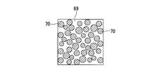
図16Bに示すように、黒色層41の形成時に用いるフォトマスク69は、複数の遮光パターン70の寸法が異なり、直径が10~25μmの範囲で分布している。このフォトマスク69を用いて黒色層41を形成すると、複数の開口部の寸法が異なる黒色層41が得られる。その後、図17Aに示すように、黒色層41をマスクとして基材39側から透明ネガレジストからなる塗膜48の露光を行うと、図17Aの符号Aで示した箇所のように、黒色層41の開口部41aの寸法が大きい箇所では拡散光Fのうち、基材39に対して大きな入射角で入射する光が黒色層41によって遮光されにくい。そのため、この箇所では基材39に対して大きな入射角で入射する光が塗膜48の露光に寄与するため、図17Bに示すように、光拡散部68の側面68cの傾斜角度が緩やかになる。
一方、図17Aの符号Bで示した箇所のように、黒色層41の開口部41aの寸法が小さい箇所では大きな入射角で入射する光が黒色層41によって遮光されやすい。そのため、この箇所では基材39に対して大きな入射角で入射する光が塗膜48の露光に寄与できないため、図17Bに示すように、光拡散部68の側面68cの傾斜角度が急になる。このように、黒色層41の開口部41aの寸法を異ならせることによって光拡散部68の光射出端面68aの寸法を異ならせるばかりでなく、側面68cの傾斜角度も異ならせることができる。勿論、第1実施形態のように、拡散光の拡散角度を場所によって変化させても良い。
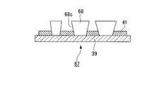
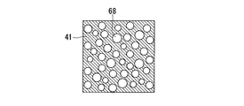
本実施形態の視野角拡大フィルム67では、複数の光拡散部68において、光射出端面68aの寸法(黒色層41の開口部の寸法)が異なり、側面68cの傾斜角度も異なっている。しかしながら、本実施形態の変形例として、図18Aおよび図18Bに示すように複数の光拡散部68の光射出端面68aの寸法は互いに異なるが、側面68cの傾斜角度は概略同じであってもよい。本変形例の光拡散部68は、露光角度や、光拡散部68の材料を最適化することで形成される。
また、本実施形態の視野角拡大フィルム67では、光拡散部68の光射出端面68aの形状は円形である。しかしながら、本実施形態の変形例として、図18Cに示すように、光拡散部68の光射出端面68aの形状は、多角形でもよいし、光拡散部68Aのように楕円形でもよい。さらに、光拡散部68は、光拡散部68Bのように隣接する光拡散部68の光射出端面68a同士が繋がっていてもよい。また、光拡散部68は、光拡散部68Cのように一部が欠けていてもよい。
本実施形態の液晶表示装置66においても、モアレが生じることがなく、表示品位を維持できる、といった第1、第2実施形態と同様の効果が得られる。また、観察角度に応じて輝度がなだらかに変化し、視野角特性を向上できる、といった第2実施形態と同様の効果が得られる。
さらに、複数の光拡散部をランダムに配置する場合、同じ大きさの光拡散部を配置しようとすると、光拡散部同士が干渉して光拡散部を配置できない箇所が多くなる。その場合、視野角拡大フィルム全体における光拡散部の占める割合が小さくなるため、バックライトから射出された光のうち、光拡散部を透過せず、黒色層に吸収される光の割合が多くなる。その結果、バックライトからの光の利用効率が低下し、正面輝度も低下する。その点、本実施形態の場合、例えば大きな光拡散部68間の隙間を小さな光拡散部68で埋めるなどして、視野角拡大フィルム67全体における光拡散部68の占める割合を高めることができる。これにより、バックライトからの光の利用効率を向上させ、正面輝度を高めることができる。
[第4実施形態]
以下、本発明の第4実施形態について、図19、図20を用いて説明する。
本実施形態の液晶表示装置の基本構成は第1実施形態と同一であり、視野角拡大フィルムの光拡散部の形状が第1実施形態と異なる。したがって、本実施形態では、液晶表示装置の基本構成の説明は省略し、視野角拡大フィルムについてのみ説明する。
図19は本実施形態の液晶表示装置を示す縦断面図である。図20は本実施形態の視野角拡大フィルムを示す縦断面図である。
図19、図20において、第1実施形態で用いた図面と共通の構成要素には同一の符号を付し、その詳細な説明は省略する。
以下、本発明の第4実施形態について、図19、図20を用いて説明する。
本実施形態の液晶表示装置の基本構成は第1実施形態と同一であり、視野角拡大フィルムの光拡散部の形状が第1実施形態と異なる。したがって、本実施形態では、液晶表示装置の基本構成の説明は省略し、視野角拡大フィルムについてのみ説明する。
図19は本実施形態の液晶表示装置を示す縦断面図である。図20は本実施形態の視野角拡大フィルムを示す縦断面図である。
図19、図20において、第1実施形態で用いた図面と共通の構成要素には同一の符号を付し、その詳細な説明は省略する。
上記の第1~第3実施形態においては、一つの光拡散部に着目したときに、光拡散部の側面は一定の傾斜角度を有している。これに対して、本実施形態の視野角拡大フィルム73は、図19および図20に示すように、各光拡散部74の側面74cが光射出端面74aから光入射端面74bにかけて凸状になだらかに湾曲しており、傾斜角度が場所によって異なっている。すなわち、各光拡散部74の側面74cの傾斜角度は、光射出端面74aから光入射端面74bにかけて連続的に変化している。その他の構成は第1の実施形態と同様である。
本実施形態の液晶表示装置72においても、モアレが生じることがなく、表示品位を維持できる、といった第1~第3実施形態と同様の効果が得られる。
また、光拡散部の側面の傾斜角度が一定である場合、画面の水平方向もしくは垂直方向に沿って観察角度を変えたときに、観察角度によっては表示ムラが視認される場合がある。この表示ムラ対策として、第2実施形態、第3実施形態では複数の光拡散部全体で側面が複数種類の傾斜角度を有していた。これに対して、本実施形態の視野角拡大フィルム73では、個々の光拡散部74においても、側面74cの場所によって傾斜角度が異なっているため、側面の傾斜角度が一定である場合に比べて光の反射角度分布が広がる。これにより、観察角度に応じて輝度がなだらかに変化し、視野角特性を向上できる。
[第5実施形態]
以下、本発明の第5実施形態について、図21、図22を用いて説明する。
本実施形態の液晶表示装置の基本構成は第1の実施形態と同一であり、視野角拡大フィルムの光拡散部の形状が第1実施形態となる。したがって、本実施形態では、液晶表示装置の基本構成の説明は省略し、視野角拡大フィルムについてのみ説明する。
図21は本実施形態の液晶表示装置を示す縦断面図である。図22は本実施形態の視野角拡大フィルムを示す平面図である。
また、図21、図22において、第1の実施形態で用いた図面と共通の構成要素には同一の符号を付し、その詳細な説明は省略する。
以下、本発明の第5実施形態について、図21、図22を用いて説明する。
本実施形態の液晶表示装置の基本構成は第1の実施形態と同一であり、視野角拡大フィルムの光拡散部の形状が第1実施形態となる。したがって、本実施形態では、液晶表示装置の基本構成の説明は省略し、視野角拡大フィルムについてのみ説明する。
図21は本実施形態の液晶表示装置を示す縦断面図である。図22は本実施形態の視野角拡大フィルムを示す平面図である。
また、図21、図22において、第1の実施形態で用いた図面と共通の構成要素には同一の符号を付し、その詳細な説明は省略する。
第1~第4実施形態では、光拡散部の各光拡散部は略円錐台形状であり、光入射端面、光射出端面の平面形状はともに円形である。これに対して、本実施形態の視野角拡大フィルム77において、各光拡散部78は、図21に示すように、八角錐台形状であり、光入射端面78b、光射出端面78aの平面形状はともに八角形である。各光拡散部78の平面形状である八角形の8本の辺のうち、互いに平行な2辺を1組とした4組の辺は、x軸に平行な方向、y軸に平行な方向、x軸と45°の角度をなす方向(x軸の正方向を基準として反時計回りに見た角度)、x軸と135°の角度をなす方向、をそれぞれ向くように配置されている。その他の構成は第1の実施形態と同様である。上記構成の視野角拡大フィルム77を作製するには、黒色層41の形成工程において、八角形の遮光パターンを有するフォトマスクを用いれば良い。
本実施形態の液晶表示装置76においても、モアレが生じることがなく、表示品位を維持できる、といった第1~第4実施形態と同様の効果が得られる。
さらに、第1~第4実施形態によれば、光拡散部の平面的な形状が円形であるため、液晶表示体6の法線方向を中心として全方位に光が拡散し、全方位に視野角拡大効果が発揮される。これに対して、本実施形態によれば、光拡散部78の平面的な形状が八角形であり、上述の4組の辺が、x軸に平行な方向、y軸に平行な方向、x軸と45°の角度をなす方向、x軸と135°の角度をなす方向をそれぞれ向いているため、光が上記の4つの方位に集中して拡散する。そのため、液晶表示装置で視野角特性が特に重要視されている、画面の水平方向、垂直方向、および斜め方向において視野角拡大効果が発揮される。なお、光拡散部78の平面的な形状は八角形に限ることなく、その他の多角形を採用することができる。その場合、多角形の形状および辺の配置に応じて光が特定の方向に集中して拡散するため、特定の観察方位において優れた視野角拡大効果を発揮する液晶表示装置が提供できる。
[第6実施形態]
以下、本発明の第6実施形態について、図23~25を用いて説明する。
本実施形態の液晶表示装置の基本構成は第1の実施形態と同一であり、視野角拡大フィルムの光拡散部の形状が第1実施形態と異なるのみである。したがって、本実施形態では、液晶表示装置の基本構成の説明は省略し、視野角拡大フィルムについてのみ説明する。
図23は本実施形態の液晶表示装置を示す縦断面図である。図24Aは本実施形態の視野角拡大フィルムを示す平面図であり、図24Bは視野角拡大フィルムの黒色層の形成に用いるフォトマスクを示す平面図である。図25は本実施形態の変形例の液晶表示装置における視野角拡大フィルムを示す平面図である。
また、図23~図25において、第1の実施形態で用いた図面と共通の構成要素には同一の符号を付し、その詳細な説明は省略する。
以下、本発明の第6実施形態について、図23~25を用いて説明する。
本実施形態の液晶表示装置の基本構成は第1の実施形態と同一であり、視野角拡大フィルムの光拡散部の形状が第1実施形態と異なるのみである。したがって、本実施形態では、液晶表示装置の基本構成の説明は省略し、視野角拡大フィルムについてのみ説明する。
図23は本実施形態の液晶表示装置を示す縦断面図である。図24Aは本実施形態の視野角拡大フィルムを示す平面図であり、図24Bは視野角拡大フィルムの黒色層の形成に用いるフォトマスクを示す平面図である。図25は本実施形態の変形例の液晶表示装置における視野角拡大フィルムを示す平面図である。
また、図23~図25において、第1の実施形態で用いた図面と共通の構成要素には同一の符号を付し、その詳細な説明は省略する。
本実施形態の視野角拡大フィルム81は、図23および図24Aに示すように、光拡散部82が存在する領域と黒色層41および空気層が存在する領域とが第1実施形態の視野角拡大フィルムと比べて逆転している。すなわち、第1実施形態の視野角拡大フィルムは円錐台状の光拡散部を有していたのに対し、本実施形態の視野角拡大フィルム81は円錐台状の空間のうち、基材39に接する部分に黒色層41、それ以外の部分に空気層を有している。したがって、本実施形態の黒色層41は、図24Aに示すように、複数の円形の黒色層41がランダムに点在し、それ以外の部分が不定形の光拡散部82となる。なお、図24Aでは、黒色層41が円形である例を示しているが、図25に示す黒色層41Aのように楕円形でもよいし、多角形でもよい。また、黒色層41Bのように隣接する黒色層の一部が繋がっていてもよい。さらに、黒色層41Cで示すように、黒色層の一具が欠けていてもよい。黒色層41の形状や寸法は、全て実質同一でもよいし、一部の形状や寸法が異なっていてもよい。
このように、本実施形態の黒色層41の形状は第1実施形態の黒色層の形状を反転させたものであり、図24Bに示すように、黒色層41を形成する際に用いるフォトマスク83は、第1実施形態で用いたフォトマスクの遮光パターンと開口部とが反転したものとなり、符号84の斜線を付した部分が遮光パターンとなる。また、本実施形態の光拡散部82は、円錐台状の空間を除く部分を埋めるように設けられており、光拡散部82の平面形状はランダムな不定形状となる。ただし、光拡散部82は、光射出端面82aと光射出端面82aよりも大きい面積の光入射端面82bとを有しており、側面82cが所定の傾斜角度を有している点では第1実施形態と同様である。
本実施形態の液晶表示装置80においても、モアレが生じることがなく、表示品位を維持できる、といった第1~第5実施形態と同様の効果が得られる。
また、黒色層41を形成する際に、開口部(光拡散部の形成領域となる部分)の寸法が微細になると、開口部に存在するブラックネガレジストが完全に抜けきらない等、黒色層41の正確なパターニングが難しい場合がある。その点、本実施形態では、点在する黒色層41を残す方法であるから、第1実施形態に比べて黒色層41のパターニングが容易になるという利点がある。
[第7実施形態]
以下、本発明の第7実施形態について、図26を用いて説明する。
本実施形態の液晶表示装置の基本構成は第1実施形態と同一であり、タッチパネルを備えた点が第1実施形態と異なっている。したがって、本実施形態では、液晶表示装置の基本構成の説明は省略し、タッチパネルの構成についてのみ説明する。
また、図26において、第1の実施形態で用いた図2と共通の構成要素には同一の符号を付し、その詳細な説明は省略する。
以下、本発明の第7実施形態について、図26を用いて説明する。
本実施形態の液晶表示装置の基本構成は第1実施形態と同一であり、タッチパネルを備えた点が第1実施形態と異なっている。したがって、本実施形態では、液晶表示装置の基本構成の説明は省略し、タッチパネルの構成についてのみ説明する。
また、図26において、第1の実施形態で用いた図2と共通の構成要素には同一の符号を付し、その詳細な説明は省略する。
本実施形態の液晶表示装置84においては、図26に示すように、バックライト2から視野角拡大フィルム7までの構成は第1実施形態と同一である。そして、視野角拡大フィルム7を構成する基材39の視認側にタッチパネル85(情報入力装置)が配置されている。以下の説明では、視野角拡大フィルム7を構成する基材39のことを「視野角拡大フィルム用基材」と称する。タッチパネル85は、視野角拡大フィルム用基材39の周縁部において両面テープ等の接着材86によって視野角拡大フィルム用基材39上に貼付されており、タッチパネル85と視野角拡大フィルム用基材39との間には接着材86の厚さ分の間隙が形成されている。すなわち、タッチパネル85と視野角拡大フィルム用基材39との間には空気層87が存在している。
タッチパネル85は、基材88と位置検出用電極89とを有している。以下の説明では、タッチパネル85を構成する基材88のことを「タッチパネル用基材」と称する。ガラス等からなるタッチパネル用基材88の一面に、ITO、ATO(Antimony-doped Tin Oxide:アンチモンがドープされた錫酸化物)等の透明導電材料からなる位置検出用電極89が形成されている。位置検出用電極89は、ITO、ATO等のスパッタリングにより形成されたものであり、数百~2kΩ/□程度の一様なシート抵抗を有している。
本実施形態では、静電容量方式のタッチパネル85が用いられている。静電容量方式のタッチパネル85では、例えばタッチパネル85を平面視したときの位置検出用電極89の4つの角部に微小な電圧が印加されている。位置検出用電極89上方の任意の位置に指を触れると、指を触れた点が人体の静電容量を介して接地される。これにより、接地点と4つの角部との間の抵抗値に応じて各角部での電圧が変化する。位置検出回路がこの電圧変化を電流変化として計測し、その計測値から接地点、すなわち指が触れた位置を検出する。
なお、本実施形態に適用可能なタッチパネルは静電容量方式に限ることはなく、抵抗膜方式、超音波方式、光学方式等、任意のタッチパネルが適用可能である。
なお、本実施形態に適用可能なタッチパネルは静電容量方式に限ることはなく、抵抗膜方式、超音波方式、光学方式等、任意のタッチパネルが適用可能である。
本実施形態の液晶表示装置84によれば、第1実施形態と同様の視野角拡大フィルム7を備えているので、視野角特性に優れ、さらに情報入力機能を備えた液晶表示装置を実現することができる。例えば使用者が広視野角の画像を見ながら指やペンでタッチパネル85に触れることによって、情報処理装置等に対話形式で情報を入力することが可能になる。
なお、本発明の態様における技術範囲は上記実施形態に限定されるものではなく、本発明の態様における趣旨を逸脱しない範囲において種々の変更を加えることが可能である。例えば上記実施形態では、表示体として液晶表示装置の例を挙げたが、これに限ることなく、有機エレクトロルミネッセンス表示装置、プラズマディスプレイ等に本発明を適用しても良い。
また、上記実施形態では、視野角拡大フィルムを液晶表示体の第2偏光板上に接着する例を示したが、視野角拡大フィルムと液晶表示体とは必ずしも接触していなくても良い。
例えば、視野角拡大フィルムと液晶表示体との間に他の光学フィルムや光学部品等が挿入されていても良い。あるいは、視野角拡大フィルムと液晶表示体とが離れた位置にあっても良い。また、有機エレクトロルミネッセンス表示装置、プラズマディスプレイ等の場合には偏光板が不要であるため、視野角拡大フィルムと偏光板とが接触することはない。
例えば、視野角拡大フィルムと液晶表示体との間に他の光学フィルムや光学部品等が挿入されていても良い。あるいは、視野角拡大フィルムと液晶表示体とが離れた位置にあっても良い。また、有機エレクトロルミネッセンス表示装置、プラズマディスプレイ等の場合には偏光板が不要であるため、視野角拡大フィルムと偏光板とが接触することはない。
また、上記実施形態における視野角拡大フィルムの基材の視認側に、反射防止層、偏光フィルター層、帯電防止層、防眩処理層、防汚処理層のうちの少なくとも一つを設けた構成としても良い。この構成によれば、基材の視認側に設ける層の種類に応じて、外光反射を低減する機能、塵埃や汚れの付着を防止する機能、傷を防止する機能等を付加することができ、視野角特性の経時劣化を防ぐことができる。
また、上記実施形態では、光拡散部の形状を円錐台状もしくは多角錐台状としたが、光拡散部の側面の傾斜角度は光軸を中心として必ずしも対称でなくても良い。上記実施形態のように光拡散部の形状を円錐台状もしくは多角錐台状とした場合には、光拡散部の側面の傾斜角度が光軸を中心として対称となるため、光軸を中心として対称的な角度分布が得られる。これに対し、表示装置の用途や使い方に応じて意図的に非対称な角度分布が要求される場合、例えば画面の上方側だけ、あるいは右側だけに視野角を広げたい等の要求がある場合には、光拡散部の側面の傾斜角度を非対称にしても良い。
その他、光拡散部や光吸収層の配置や形状、視野角拡大フィルムの各部の寸法や材料、製造プロセスにおける製造条件等に関する具体的な構成は上記実施形態に限ることなく、適宜変更が可能である。
本発明の態様は、液晶表示装置、有機エレクトロルミネッセンス表示装置、プラズマディスプレイ等の各種表示装置に利用可能である。
1,61,66,72,76,80,84…液晶表示装置(表示装置)、6…液晶表示体(表示体)、7,62,67,73,77,81…視野角拡大フィルム(視野角拡大部材)、39…基材、40,63,68,74,78,82…光拡散部、40a,63a,68a,74a,78a,82a…光射出端面、40b,63b,68b,74b,78b,82b…光入射端面、40c,63c,68c,74c,78c,82c…側面、41…黒色層(光吸収層)、85…タッチパネル(情報入力装置)。
Claims (14)
- 光透過性を有する基材と、前記基材の一面に形成された複数の光拡散部と、前記基材の一面のうち前記光拡散部の形成領域以外の領域に形成された光吸収層と、を備え、
前記光拡散部が、前記基材側に光射出端面を有するとともに前記基材側と反対側に前記光射出端面の面積よりも大きい面積の光入射端面を有し、
前記光拡散部の前記光入射端面から前記光射出端面までの高さが前記光吸収層の層厚よりも大きく、
前記複数の光拡散部が、前記基材の一面にランダムに配置されている光拡散部材。 - 前記複数の光拡散部間の間隙に空気が存在している請求項1に記載の光拡散部材。
- 前記複数の光拡散部のうち、少なくとも一つの光拡散部の前記光射出端面の寸法が他の光拡散部の前記光射出端面の寸法と異なる請求項1に記載の光拡散部材。
- 前記複数の光拡散部のうち、少なくとも一つの光拡散部の側面の傾斜角度が他の光拡散部の側面の傾斜角度と異なる請求項1に記載の光拡散部材。
- 前記複数の光拡散部のうち、少なくとも一つの光拡散部の側面の傾斜角度が連続的に変化する請求項1に記載の光拡散部材。
- 前記基材の一面の法線方向から見た前記光拡散部の平面的な形状が、円形もしくは多角形である請求項1に記載の光拡散部材。
- 光透過性を有する基材と、前記基材の一面に点在して形成された複数の光吸収層と、前記基材の一面のうち前記光吸収層の形成領域以外の領域に形成された光拡散部と、を備え、
前記光拡散部が、前記基材側に光射出端面を有するとともに前記基材側と反対側に前記光射出端面よりも大きい面積の光入射端面を有し、
前記光拡散部の前記光入射端面から前記光射出端面までの高さが前記光吸収層の層厚よりも大きく、
前記光拡散部が、前記基材の一面の法線方向から見てランダムな形状を有している光拡散部材。 - 前記基材の前記一面と反対側の面に、反射防止層、偏光フィルター層、帯電防止層、防眩処理層、防汚処理層のうちの少なくとも一つが設けられている請求項1に記載の光拡散部材。
- 光透過性を有する基材の一面に、少なくとも一つの開口部を有する光吸収層を形成し、
前記基材の一面に、前記光吸収層を覆うように光透過性を有するネガ型感光性樹脂層を形成し、
前記光吸収層および前記ネガ型感光性樹脂層を形成した前記基材の一面と反対側の面から、前記光吸収層の開口部を通して前記ネガ型感光性樹脂層に対して拡散光を照射し、
前記拡散光の照射が終わった前記ネガ型感光性樹脂層を現像し、前記基材側に光射出端面を有するとともに前記基材側と反対側に前記光射出端面の面積よりも大きい面積の光入射端面を有する光拡散部を前記基材の一面に形成する光拡散部材の製造方法。 - 表示体と、前記表示体の視認側に設けられ、前記表示体から入射される光の角度分布を入射前よりも広げた状態にして光を射出させる視野角拡大部材と、を備え、
前記視野角拡大部材は、光透過性を有する基材と、前記基材の一面に形成された複数の光拡散部と、前記基材の一面のうち前記光拡散部の形成領域以外の領域に形成された光吸収層と、を備え、
前記光拡散部が、前記基材側に光射出端面を有するとともに前記基材側と反対側に前記光射出端面の面積よりも大きい面積の光入射端面を有し、
前記光拡散部の前記光入射端面から前記光射出端面までの高さが前記光吸収層の層厚よりも大きく、
前記複数の光拡散部が、前記基材の一面にランダムに配置されている表示装置。 - 前記表示体が、表示画像を形成する複数の画素を有し、
前記光拡散部材の前記複数の光拡散部のうち、隣接する光拡散部間の平均間隔が、前記表示体の前記画素間の間隔よりも小さい請求項10に記載の表示装置。 - 前記視野角拡大部材の視認側に、情報入力装置が設けられている請求項10に記載の表示装置。
- 前記表示体が、光源と、前記光源からの光を変調する光変調素子と、を有し、
前記光源が指向性を有する光を射出する請求項10に記載の表示装置。 - 前記表示体が液晶表示素子である請求項10に記載の表示装置。
Priority Applications (1)
| Application Number | Priority Date | Filing Date | Title |
|---|---|---|---|
| US13/880,181 US9274255B2 (en) | 2010-10-21 | 2011-10-18 | Light-diffusion member, manufacturing method thereof, and display device |
Applications Claiming Priority (2)
| Application Number | Priority Date | Filing Date | Title |
|---|---|---|---|
| JP2010-236513 | 2010-10-21 | ||
| JP2010236513 | 2010-10-21 |
Publications (1)
| Publication Number | Publication Date |
|---|---|
| WO2012053501A1 true WO2012053501A1 (ja) | 2012-04-26 |
Family
ID=45975212
Family Applications (1)
| Application Number | Title | Priority Date | Filing Date |
|---|---|---|---|
| PCT/JP2011/073897 Ceased WO2012053501A1 (ja) | 2010-10-21 | 2011-10-18 | 光拡散部材およびその製造方法、表示装置 |
Country Status (2)
| Country | Link |
|---|---|
| US (1) | US9274255B2 (ja) |
| WO (1) | WO2012053501A1 (ja) |
Cited By (7)
| Publication number | Priority date | Publication date | Assignee | Title |
|---|---|---|---|---|
| US20130229603A1 (en) * | 2012-03-05 | 2013-09-05 | Japan Display West Inc. | Display device and anisotropic scatterer |
| WO2013157431A1 (ja) * | 2012-04-18 | 2013-10-24 | シャープ株式会社 | 光制御部材およびその製造方法、表示装置 |
| WO2014045988A1 (ja) * | 2012-09-21 | 2014-03-27 | シャープ株式会社 | 液晶表示装置 |
| WO2014084261A1 (ja) * | 2012-11-30 | 2014-06-05 | シャープ株式会社 | 光制御フィルム及び表示装置 |
| WO2014097960A1 (ja) * | 2012-12-18 | 2014-06-26 | シャープ株式会社 | 液晶表示装置 |
| WO2015064568A1 (ja) * | 2013-10-30 | 2015-05-07 | シャープ株式会社 | 光拡散部材の製造方法および製造装置 |
| WO2024221067A1 (pt) | 2023-04-26 | 2024-10-31 | Nabhan Jose Marcos | Sistema de detecção para remediar altas concentrações de dióxido de carbono no interior do habitáculo de veículos automotores |
Families Citing this family (10)
| Publication number | Priority date | Publication date | Assignee | Title |
|---|---|---|---|---|
| JP2014142366A (ja) * | 2011-05-13 | 2014-08-07 | Sharp Corp | 光拡散部材およびその製造方法、表示装置 |
| WO2014024814A1 (ja) * | 2012-08-10 | 2014-02-13 | シャープ株式会社 | 液晶表示装置 |
| JP2014102469A (ja) * | 2012-11-22 | 2014-06-05 | Sharp Corp | 液晶表示装置 |
| US10162214B2 (en) * | 2014-05-21 | 2018-12-25 | Sharp Kabushiki Kaisha | Liquid crystal display device, optical control member, and base material for manufacturing optical control member |
| WO2016093307A1 (ja) * | 2014-12-12 | 2016-06-16 | シャープ株式会社 | 表示装置、接着層付き光拡散部材及びその製造方法 |
| KR102769963B1 (ko) * | 2016-10-31 | 2025-02-17 | 엘지디스플레이 주식회사 | 액정표시장치 |
| CN110083005A (zh) * | 2018-01-23 | 2019-08-02 | 台湾扬昕股份有限公司 | 背投屏幕 |
| CN208110256U (zh) * | 2018-03-21 | 2018-11-16 | 中强光电股份有限公司 | 背投影幕 |
| DE102018208185A1 (de) | 2018-05-24 | 2019-11-28 | Robert Bosch Gmbh | Optisches Element zur Lichtkonzentration und Herstellungsverfahren für ein optisches Element zur Lichtkonzentration |
| CN111796349A (zh) * | 2020-07-02 | 2020-10-20 | Tcl华星光电技术有限公司 | 一种视角扩散膜片及显示面板 |
Citations (7)
| Publication number | Priority date | Publication date | Assignee | Title |
|---|---|---|---|---|
| JP2003504691A (ja) * | 1999-07-07 | 2003-02-04 | スリーエム イノベイティブ プロパティズ カンパニー | 内部反射を用いた背面投射スクリーンおよびその製法 |
| JP2004516525A (ja) * | 2000-12-27 | 2004-06-03 | スリーエム イノベイティブ プロパティズ カンパニー | 微細構造付き背面投射スクリーン |
| JP2004361685A (ja) * | 2003-06-04 | 2004-12-24 | Ricoh Co Ltd | 透過型スクリーンシート及びこれを用いた画像表示装置 |
| JP2007514202A (ja) * | 2003-12-11 | 2007-05-31 | スリーエム イノベイティブ プロパティズ カンパニー | 光吸収材料を有する微細構造化スクリーンおよび製造方法 |
| JP2007517929A (ja) * | 2003-12-11 | 2007-07-05 | スリーエム イノベイティブ プロパティズ カンパニー | 微細構造スクリーン用組成物 |
| JP2007519034A (ja) * | 2003-12-11 | 2007-07-12 | スリーエム イノベイティブ プロパティズ カンパニー | 微細構造スクリーン、および同時押出を使用した製造方法 |
| JP2010079292A (ja) * | 2008-08-27 | 2010-04-08 | Toppan Printing Co Ltd | 光学部品の製造用金型、光学部品の製造方法、光学部品、および液晶表示ディスプレイユニット |
Family Cites Families (4)
| Publication number | Priority date | Publication date | Assignee | Title |
|---|---|---|---|---|
| US6002464A (en) * | 1996-05-13 | 1999-12-14 | Kuraray Co., Ltd. | Light diffusing sheet having a layer incorporated with light diffusing material and a layer with a corrugated surface |
| KR101255297B1 (ko) * | 2008-03-11 | 2013-04-15 | 엘지디스플레이 주식회사 | 액정표시장치 |
| US20110019128A1 (en) * | 2008-03-27 | 2011-01-27 | Sharp Kabushiki Kaisha | Optical member, lighting device, display device, television receiver and manufacturing method of optical member |
| JP5569008B2 (ja) * | 2009-06-07 | 2014-08-13 | ソニー株式会社 | バックライトおよび液晶表示装置 |
-
2011
- 2011-10-18 US US13/880,181 patent/US9274255B2/en not_active Expired - Fee Related
- 2011-10-18 WO PCT/JP2011/073897 patent/WO2012053501A1/ja not_active Ceased
Patent Citations (7)
| Publication number | Priority date | Publication date | Assignee | Title |
|---|---|---|---|---|
| JP2003504691A (ja) * | 1999-07-07 | 2003-02-04 | スリーエム イノベイティブ プロパティズ カンパニー | 内部反射を用いた背面投射スクリーンおよびその製法 |
| JP2004516525A (ja) * | 2000-12-27 | 2004-06-03 | スリーエム イノベイティブ プロパティズ カンパニー | 微細構造付き背面投射スクリーン |
| JP2004361685A (ja) * | 2003-06-04 | 2004-12-24 | Ricoh Co Ltd | 透過型スクリーンシート及びこれを用いた画像表示装置 |
| JP2007514202A (ja) * | 2003-12-11 | 2007-05-31 | スリーエム イノベイティブ プロパティズ カンパニー | 光吸収材料を有する微細構造化スクリーンおよび製造方法 |
| JP2007517929A (ja) * | 2003-12-11 | 2007-07-05 | スリーエム イノベイティブ プロパティズ カンパニー | 微細構造スクリーン用組成物 |
| JP2007519034A (ja) * | 2003-12-11 | 2007-07-12 | スリーエム イノベイティブ プロパティズ カンパニー | 微細構造スクリーン、および同時押出を使用した製造方法 |
| JP2010079292A (ja) * | 2008-08-27 | 2010-04-08 | Toppan Printing Co Ltd | 光学部品の製造用金型、光学部品の製造方法、光学部品、および液晶表示ディスプレイユニット |
Cited By (20)
| Publication number | Priority date | Publication date | Assignee | Title |
|---|---|---|---|---|
| US9274365B2 (en) * | 2012-03-05 | 2016-03-01 | Japan Display Inc. | Display device and anisotropic scatterer |
| CN103293752A (zh) * | 2012-03-05 | 2013-09-11 | 株式会社巴川制纸所 | 显示装置和各向异性散射体 |
| US20130229603A1 (en) * | 2012-03-05 | 2013-09-05 | Japan Display West Inc. | Display device and anisotropic scatterer |
| CN103293752B (zh) * | 2012-03-05 | 2017-03-29 | 株式会社巴川制纸所 | 显示装置和各向异性散射体 |
| US9772430B2 (en) | 2012-04-18 | 2017-09-26 | Sharp Kabushiki Kaisha | Light control member, method for manufacturing same, and display device |
| WO2013157431A1 (ja) * | 2012-04-18 | 2013-10-24 | シャープ株式会社 | 光制御部材およびその製造方法、表示装置 |
| JP2016177312A (ja) * | 2012-09-21 | 2016-10-06 | シャープ株式会社 | 液晶表示装置 |
| WO2014045988A1 (ja) * | 2012-09-21 | 2014-03-27 | シャープ株式会社 | 液晶表示装置 |
| CN104641283A (zh) * | 2012-09-21 | 2015-05-20 | 夏普株式会社 | 液晶显示装置 |
| US20150219957A1 (en) * | 2012-09-21 | 2015-08-06 | Sharp Kabushiki Kaisha | Liquid crystal display device |
| CN104641283B (zh) * | 2012-09-21 | 2017-04-26 | 夏普株式会社 | 液晶显示装置 |
| WO2014084261A1 (ja) * | 2012-11-30 | 2014-06-05 | シャープ株式会社 | 光制御フィルム及び表示装置 |
| US9541787B2 (en) | 2012-11-30 | 2017-01-10 | Sharp Kabushiki Kaisha | Light control film including light control layer with reflection surface and display device including same |
| JP2014109625A (ja) * | 2012-11-30 | 2014-06-12 | Sharp Corp | 光制御フィルム及び表示装置 |
| WO2014097960A1 (ja) * | 2012-12-18 | 2014-06-26 | シャープ株式会社 | 液晶表示装置 |
| US9829737B2 (en) | 2012-12-18 | 2017-11-28 | Sharp Kabushiki Kaisha | Liquid crystal display device having low viewing angle dependency |
| WO2015064568A1 (ja) * | 2013-10-30 | 2015-05-07 | シャープ株式会社 | 光拡散部材の製造方法および製造装置 |
| US10197712B2 (en) | 2013-10-30 | 2019-02-05 | Sharp Kabushiki Kaisha | Light-diffusing-member manufacturing method and manufacturing device |
| WO2024221067A1 (pt) | 2023-04-26 | 2024-10-31 | Nabhan Jose Marcos | Sistema de detecção para remediar altas concentrações de dióxido de carbono no interior do habitáculo de veículos automotores |
| EP4703162A1 (en) | 2023-04-26 | 2026-03-04 | Nabhan, José Marcos | Detection system for remedying high concentrations of carbon dioxide inside the passenger compartment of motor vehicles |
Also Published As
| Publication number | Publication date |
|---|---|
| US20140160410A1 (en) | 2014-06-12 |
| US9274255B2 (en) | 2016-03-01 |
Similar Documents
| Publication | Publication Date | Title |
|---|---|---|
| CN202512257U (zh) | 光扩散部件和其显示装置 | |
| JP6249420B2 (ja) | 光拡散部材およびその製造方法、表示装置およびその製造方法 | |
| WO2012053501A1 (ja) | 光拡散部材およびその製造方法、表示装置 | |
| US8926157B2 (en) | Light diffusing member and method of manufacturing the same, and display device | |
| JP5908089B2 (ja) | 光拡散タッチパネルおよびその製造方法、表示装置 | |
| JP5916245B2 (ja) | 液晶表示装置、光制御フィルム、表示装置 | |
| WO2011158752A1 (ja) | 表示装置およびその製造方法 | |
| JPWO2013146353A1 (ja) | 光制御フィルム、表示装置、および光制御フィルムの製造方法 | |
| JP5863215B2 (ja) | 光拡散部材およびその製造方法、表示装置 | |
| WO2012081410A1 (ja) | 光拡散部材およびその製造方法、表示装置 | |
| JP2014142368A (ja) | 光拡散部材およびその製造方法、表示装置 | |
| JP6103377B2 (ja) | 表示装置及びその製造方法 | |
| JP5860142B2 (ja) | 光制御部材およびその製造方法、表示装置 | |
| WO2015002072A1 (ja) | 光拡散部材及び表示装置 | |
| WO2014092017A1 (ja) | 光拡散部材及び表示装置 | |
| JP2014013315A (ja) | 光制御部材およびその製造方法、表示装置 | |
| JP5859928B2 (ja) | 光拡散部材およびその製造方法、表示装置 | |
| JP2013225008A (ja) | 光制御フィルム、表示装置、および光制御フィルムの製造方法 | |
| WO2015005284A1 (ja) | 光拡散部材及び表示装置 | |
| JP2014032324A (ja) | 光拡散部材、光拡散部材の製造方法、及び表示装置 | |
| JP2013228528A (ja) | 光制御フィルム、表示装置、および光制御フィルムの製造方法 |
Legal Events
| Date | Code | Title | Description |
|---|---|---|---|
| 121 | Ep: the epo has been informed by wipo that ep was designated in this application |
Ref document number: 11834340 Country of ref document: EP Kind code of ref document: A1 |
|
| NENP | Non-entry into the national phase |
Ref country code: DE |
|
| WWE | Wipo information: entry into national phase |
Ref document number: 13880181 Country of ref document: US |
|
| 122 | Ep: pct application non-entry in european phase |
Ref document number: 11834340 Country of ref document: EP Kind code of ref document: A1 |
|
| NENP | Non-entry into the national phase |
Ref country code: JP |