WO2012033152A1 - 多層配線基板の製造方法 - Google Patents
多層配線基板の製造方法 Download PDFInfo
- Publication number
- WO2012033152A1 WO2012033152A1 PCT/JP2011/070437 JP2011070437W WO2012033152A1 WO 2012033152 A1 WO2012033152 A1 WO 2012033152A1 JP 2011070437 W JP2011070437 W JP 2011070437W WO 2012033152 A1 WO2012033152 A1 WO 2012033152A1
- Authority
- WO
- WIPO (PCT)
- Prior art keywords
- resin layer
- layer
- group
- temporary support
- resin
- Prior art date
- Legal status (The legal status is an assumption and is not a legal conclusion. Google has not performed a legal analysis and makes no representation as to the accuracy of the status listed.)
- Ceased
Links
Images



Classifications
-
- H—ELECTRICITY
- H05—ELECTRIC TECHNIQUES NOT OTHERWISE PROVIDED FOR
- H05K—PRINTED CIRCUITS; CASINGS OR CONSTRUCTIONAL DETAILS OF ELECTRIC APPARATUS; MANUFACTURE OF ASSEMBLAGES OF ELECTRICAL COMPONENTS
- H05K3/00—Apparatus or processes for manufacturing printed circuits
- H05K3/40—Forming printed elements for providing electric connections to or between printed circuits
- H05K3/42—Plated through-holes or plated via connections
- H05K3/421—Blind plated via connections
-
- H—ELECTRICITY
- H05—ELECTRIC TECHNIQUES NOT OTHERWISE PROVIDED FOR
- H05K—PRINTED CIRCUITS; CASINGS OR CONSTRUCTIONAL DETAILS OF ELECTRIC APPARATUS; MANUFACTURE OF ASSEMBLAGES OF ELECTRICAL COMPONENTS
- H05K2201/00—Indexing scheme relating to printed circuits covered by H05K1/00
- H05K2201/01—Dielectrics
- H05K2201/0183—Dielectric layers
- H05K2201/0195—Dielectric or adhesive layers comprising a plurality of layers, e.g. in a multilayer structure
-
- H—ELECTRICITY
- H05—ELECTRIC TECHNIQUES NOT OTHERWISE PROVIDED FOR
- H05K—PRINTED CIRCUITS; CASINGS OR CONSTRUCTIONAL DETAILS OF ELECTRIC APPARATUS; MANUFACTURE OF ASSEMBLAGES OF ELECTRICAL COMPONENTS
- H05K3/00—Apparatus or processes for manufacturing printed circuits
- H05K3/46—Manufacturing multilayer circuits
- H05K3/4644—Manufacturing multilayer circuits by building the multilayer layer by layer, i.e. build-up multilayer circuits
- H05K3/4661—Adding a circuit layer by direct wet plating, e.g. electroless plating; insulating materials adapted therefor
Definitions
- the present invention relates to a method for manufacturing a multilayer wiring board.
- Patent Document 4 proposes a method for manufacturing a multilayer wiring board in which interlayer connection by vias is made and a multilayer wiring board having fine wiring can be manufactured by a simple method. Specifically, in this method, first, an insulating layer is formed on the surface of a substrate having a portion that can conduct electricity, and then the insulating layer is partially removed by a laser or a drill to form a via hole. . Thereafter, a desmear process is performed on the surface on which the via hole is formed, and the residue of the insulating layer at the bottom of the via hole is removed.
- a resin layer is formed on the surface on which the desmear treatment has been performed using a liquid composition containing a resin having a predetermined functional group. Thereafter, the resin layer formed at the bottom of the via hole is removed by applying a treatment liquid, and a plating catalyst is applied to the remaining resin layer, followed by plating.
- a resin layer is formed using a liquid composition on an insulating layer in which a via hole is formed.
- the liquid composition penetrates into the via hole, it is necessary to remove unnecessary resin accumulated in the via hole.
- initial conduction failure is likely to occur, and the required yield level has not been reached recently. Further improvements were needed.
- the present invention can produce a metal wiring with high definition and excellent adhesion, and can produce a multilayer wiring board with excellent via connection reliability with high yield. It aims at providing the manufacturing method of the outstanding multilayer wiring board.
- the temperature T of the resin layer when laminating is not less than the glass transition temperature of the resin layer and not more than the glass transition temperature + 60 ° C., and the Young's modulus E (T) of the resin layer at the temperature T Is 0.16 ⁇ 10 6 to 100 ⁇ 10 6 Pa, and the elongation at break of the resin layer is 100% or less,
- the pressure P applied to the laminated film for resin layer formation and Log (E (T)) are represented by the following formulas (I) to (I) shown in FIG. A manufacturing method of a multilayer wiring board existing in a range surrounded by a straight line represented by IV).
- the temperature of the resin layer is 0 to 40 ° C., Interfacial peel strength ⁇ (A1) per unit area between the resin layer and the insulating layer, interfacial peel strength ⁇ (B1) per unit area between the resin layer and the temporary support, and fracture of the resin layer
- a laminated film for forming a resin layer comprising: a temporary support; and a resin layer containing a polymer containing a polymerizable group and a functional group that forms an interaction with the plating catalyst or a precursor thereof on the temporary support.
- the temperature T of the adhesion assisting layer and the resin layer when laminating is not less than the glass transition temperature of each of the adhesion assisting layer and the resin layer and not more than the glass transition temperature + 60 ° C., and the temperature T
- the Young's modulus E (T) of the adhesion auxiliary layer and the resin layer is 0.16 ⁇ 10 6 to 100 ⁇ 10 6 Pa, and the elongation at break of the adhesion auxiliary layer and the resin layer is 100% or less
- a method for manufacturing a substrate can be provided.
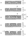
- (A) to (E) are schematic cross-sectional views from the substrate to the multilayer wiring substrate, which sequentially show the respective manufacturing steps in the method for manufacturing a multilayer wiring substrate of the present invention.
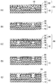
- (A) to (E) are schematic cross-sectional views from the substrate to the multilayer wiring substrate, which sequentially show the respective manufacturing steps in another embodiment of the method for manufacturing a multilayer wiring substrate of the present invention. It is a figure showing the range prescribed
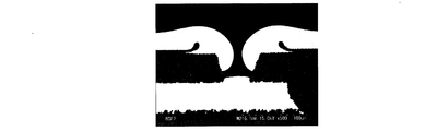
- One of the features of the production method of the present invention is that a laminated film for forming a resin layer including a temporary support and a resin layer is disposed on an insulating layer in which via holes are formed, and then the temporary support is peeled off. There is. In this procedure, when the temporary support is peeled from the laminated body, stress concentration occurs at the outer peripheral position of the via hole, so that the resin layer is cut along the outer peripheral shape of the via hole.
- the resin layer on the temporary support that is not in intimate contact with the insulating layer remains on the temporary support as it is, and is removed from the laminate together with the temporary support peeling, so that the resin layer is substantially only on the insulating layer.
- this method does not use a liquid composition containing an organic solvent, so that it can be said to be an excellent method from the environmental and process aspects.
- the manufacturing method includes the following six steps.
- a step of forming an insulating layer on the surface of a wiring board having metal wiring (B) A step of forming a via hole so as to penetrate the insulating layer and reach the metal wiring (C) After the step (B), Step (D) of performing desmear treatment After the step (C), a polymer containing a temporary support, a functional group that interacts with the plating catalyst or its precursor on the temporary support, and a polymerizable group
- an insulating layer is formed on the surface of a wiring board provided with metal wiring. More specifically, as shown in FIG. 1A, in this step, the wiring substrate 10 in which the metal wiring 14 is formed on the substrate 12 and the insulating layer 16 provided on the wiring substrate 10 are provided. A laminated body is provided. The wiring board 10 and the insulating layer 16 will be described in detail below.
- the wiring board 10 used in the present invention may be any board having the metal wiring 14 on one side or both sides of the board 12, for example. Further, as shown in FIG. 1, the metal wiring 14 may be formed in a pattern with respect to the surface of the substrate, or may be formed on the entire surface. Typically, those formed by a subtractive method using an etching process and those formed by a semi-additive method using electrolytic plating may be used, and those formed by any method may be used. More specifically, the wiring board 10 may be a double-sided or single-sided copper-clad laminate (CCL), or a copper-clad laminate made of a copper film in a pattern, which is a flexible substrate. It may be a rigid substrate.
- CCL copper-clad laminate
- paper / phenolic resin copper-clad laminates (FR-1, FR-2, XXXPc, XPc), paper / epoxy resin copper-clad laminates as paper base copper-clad laminates (FR-3), paper / polyester copper-clad laminate, and glass substrate / copper-clad laminate, glass cloth / epoxy resin copper-clad laminate (FR-4, G10), heat-resistant glass cloth / epoxy resin copper Tension laminate (FR-5, G11), glass cloth / polyimide resin copper clad laminate (GPY), glass cloth / fluororesin copper clad laminate, multilayer materials (prepreg / thin FR-4, FR- 5, GPY), multilayer copper clad laminates with inner circuit (FR-4, FR-5, GPY), etc., and as composite copper clad laminates, epoxy, composites, paper, glass cloth, epoxy resin Copper-clad laminate (CEM-1), glass nonwoven fabric / glass cloth / epoxy resin copper clad laminate (CEM
- copper-clad boards such as polyester base, polyimide base, glass epoxy base, polysulfone base, polyetherimide base, polyether ketone base, etc. are mentioned.
- the copper clad laminated board which used the inorganic material as the base material is mentioned,
- the copper clad board etc. which used alumina, aluminum nitride, silicon carbide, a low-temperature baking ceramic etc. are mentioned as a base material.
- Examples of the material constituting the substrate 12 in the wiring substrate 10 include a glass epoxy substrate, a BT resin, an alumina substrate, a polyimide film, a polyamide film, a liquid crystal film, and an aramid. Of these, a glass epoxy substrate and a BT resin are preferable from the viewpoint of multilayering and productivity of the substrate.
- Examples of the material constituting the metal wiring 14 include copper, silver, tin, palladium, gold, nickel, chromium, tungsten, indium, zinc, or gallium.
- the insulating layer 16 is a layer provided to ensure insulation reliability in the multilayer wiring board, and the formation method thereof is not particularly limited. More specifically, an insulating resin composition containing an insulating resin is applied onto the wiring substrate 10 to form an insulating layer 16 (application method), or an insulating layer 16 containing an insulating resin is formed. The method of laminating on the wiring board 10 etc. is mentioned.
- the thickness of the insulating layer 16 is appropriately selected according to the purpose of use of the multilayer wiring board, but is preferably 10 to 150 ⁇ m, more preferably 20 to 100 ⁇ m.
- the “insulating resin” in the present invention means a resin having an insulating property that can be used for a known insulating film or insulating layer, and is not a perfect insulator.
- any resin having insulating properties according to the purpose can be applied to the present invention.
- the insulating resin may be, for example, a thermosetting resin, a thermoplastic resin, or a mixture thereof.
- the thermosetting resin include an epoxy resin, a phenol resin, a polyimide resin, a polyester resin, and a bismaleimide. Examples thereof include resins, polyolefin resins, isocyanate resins and the like.
- the thermoplastic resin include phenoxy resin, polyether sulfone, polysulfone, polyphenylene sulfone, polyphenylene sulfide, polyphenyl ether, polyether imide, and the like.
- the insulating resin composition used for forming the insulating layer 16 contains a compound having a polymerizable double bond, specifically an acrylate or methacrylate compound, in order to promote crosslinking.
- a compound having a polymerizable double bond specifically an acrylate or methacrylate compound, in order to promote crosslinking.
- polyfunctional ones are preferred.
- the insulating resin composition may be provided with a filler (for example, silica, alumina, clay, talc, etc.), a colorant, a flame retardant, an adhesion-imparting agent, a silane coupling agent, and an antioxidant as necessary.
- a filler for example, silica, alumina, clay, talc, etc.
- a colorant for example, silica, alumina, clay, talc, etc.
- a flame retardant for example, silica, alumina, clay, talc, etc.
- an adhesion-imparting agent for example, silane coupling agent, and an antioxidant
- an antioxidant for example, silica, silica, alumina, clay, talc, etc.
- an ultraviolet absorber may be added.
- any of them is preferably added in the range of 1 to 200% by mass, more preferably in the range of 10 to 80% by mass with respect to the resin. Is done.
- a via hole is formed in the insulating layer formed in the step (A) so as to penetrate the insulating layer and reach the metal wiring. More specifically, as shown in FIG. 1B, in this step, a part of the insulating layer 16 is removed and a via hole 18 is formed. As shown in FIG. 1B, the via hole 18 penetrates the insulating layer 16 and reaches the vicinity of the surface of the metal wiring 14. The via hole 18 is provided to electrically connect a metal layer 28 (described later) formed on the insulating layer and the metal wiring 14.
- the method for forming the via hole 18 is not particularly limited, and a known method is employed. Of these, laser processing or drilling is preferred from the viewpoint of easy control of the diameter of the via hole to be formed and alignment.
- the laser used for laser processing is not particularly limited as long as the insulating layer 16 can be removed and the via hole 18 having a desired diameter can be formed.
- an excimer laser, a carbon dioxide laser (CO 2 laser), a UV-YAG laser, and the like are used from the viewpoint of excellent workability, that is, efficient ablation and excellent productivity. Of these, a carbon dioxide laser and a UV-YAG laser are preferable from the viewpoint of cost merit.
- the drilling is not particularly limited as long as the insulating layer 16 can be removed and the via hole 18 having a desired diameter can be formed, but the spin drill method is generally used from the viewpoint of productivity and small diameter via workability. Used for.
- the diameter of the via hole 18 formed in this step is appropriately selected according to the purpose of use, but the top diameter ( ⁇ ) is 10 in terms of downsizing the substrate and increasing the density of the wiring. It is preferable that the bottom diameter ( ⁇ ) is 10 to 150 ⁇ m, the top diameter ( ⁇ ) is 10 to 60 ⁇ m, and the bottom diameter ( ⁇ ) is 10 to 60 ⁇ m.
- a desmear process for removing smear (residue) remaining in the via hole 18 formed in the step (B) is performed.
- the insulating layer 16 is partially removed by laser processing, drilling, or the like, the molten material when the resin melts or decomposes, the decomposed material adheres to the side surface or bottom of the via hole 18, and the bottom of the via hole 18
- the insulating layer 16 may remain at the bottom of the via hole by adjusting the laser processing so as not to directly affect the metal wiring 14 existing in the hole. In this step, such a residue is removed.
- the desmear treatment method is not particularly limited, and a known method is adopted. However, the desmear treatment is performed by a method of roughening a wall surface and a bottom surface of the hole portion of the via hole 18 by a dry method and / or a wet method. Examples of the dry roughening method include mechanical polishing such as buffing and sandblasting, plasma etching, and the like. On the other hand, wet roughening methods include chemical methods such as a method using an oxidizing agent such as permanganate, dichromate, ozone, hydrogen peroxide / sulfuric acid, nitric acid, or a method using a strong base or a resin swelling solvent. Examples include chemical treatment. From the simplicity of the process, chemical treatment using permanganate or the like is preferable.
- a commercial product MLB211 manufactured by Rohm and Haas Electronic Materials Co., Ltd.
- a swelling bath containing 20% by volume and cue deposit Z10% by volume.
- an etching bath containing 10% by volume of MLB213A (Rohm and Haas Electronic Materials Co., Ltd.) and 15% by volume of MLB213B (Rohm and Haas Electronic Materials Co., Ltd.) at 55 to 85 ° C.
- Examples of the known method include immersion for 2 to 15 minutes and immersion in a neutralization bath containing 20% by volume of MLB 216-2 (Rohm and Haas Electronic Materials Co., Ltd.) at 35 to 55 ° C. for 2 to 10 minutes. .
- the residue of the insulating layer 16 on the wall surface and bottom of the via hole 18 can be removed. Since the desmear process is performed on the entire surface of the substrate, the residue of the insulating layer 16 at the bottom of the via hole 18 is removed, and the upper portion of the insulating layer 16 and the inside of the via hole 18 are roughened.
- a resin layer comprising a temporary support, and a resin layer containing a polymer containing a polymerizable group and a functional group that forms an interaction with the plating catalyst or its precursor on the temporary support.
- the forming laminated film is laminated on the insulating layer so that the resin layer and the insulating layer subjected to the desmear treatment are in contact with each other to obtain a laminated body. More specifically, as shown in FIG. 1C, in this step, a resin layer including a temporary support 22 and a resin layer 20 provided on the temporary support 22 on the insulating layer 16.
- the forming laminated film 24 is laminated so that the resin layer 20 is in contact with the insulating layer 16 to obtain a laminated body 26.
- the method of laminating the resin layer forming laminated film 24 on the insulating layer 16 so that the resin layer 20 is in contact with the insulating layer 16 is not particularly limited, and may be a batch type or a continuous type in a roll. .
- the temperature T of the resin layer 20 when laminating the laminated film 24 for resin layer formation is such that the adhesion between the resin layer 20 and the insulating layer 16 is excellent, and the breaking strength of the resin layer 20 is reduced. It is not less than the glass transition temperature of the resin layer and not more than (glass transition temperature + 60 ° C.). In particular, the range of the temperature T is preferably the glass transition temperature of the resin layer + 10 ° C.
- the glass transition temperature of the resin layer varies depending on the polymer structure described later, but is preferably 0 to 140 ° C., more preferably 20 to 120 ° C., from the viewpoint that the effects of the present invention are more excellent.
- the Young's modulus of the resin layer 20 is 0.16 ⁇ 10 6 to 100 ⁇ 10 6 Pa when the temperature T is in the above range because the adhesion between the resin layer 20 and the insulating layer 16 is excellent. Of these, 0.5 ⁇ 10 6 to 10 ⁇ 10 6 Pa is preferable, and 1 ⁇ 10 6 to 5 ⁇ 10 6 Pa is more preferable in that the yield of the obtained multilayer wiring board is more excellent. . If the Young's modulus is less than 0.16 ⁇ 10 6 Pa, the resin layer 20 enters the via hole 18 and fills the via hole 18. If it exceeds 100 ⁇ 10 6 Pa, the resin layer 20 and the insulating layer 16 The adhesion of is impaired.
- the elongation at break of the resin layer 20 is 100% or less, and is preferably 1 to 100% from the viewpoint of better adhesion between the resin layer 20 and the insulating layer 16. Among these, 3 to 100% is preferable, and 5 to 50% is more preferable in that the yield of the manufacturing method of the multilayer wiring board is more excellent. If the elongation at break is more than 100%, it is difficult to cut out the resin layer 20 during lamination, and the resin layer 20 enters the via hole, and the resin pool is likely to occur. Further, even if the removal of the cutout can be achieved at the time of peeling the temporary support, the cutout shape tends to be distorted because the plastic deformation amount of the resin layer 20 is large.
- the resin layer 20 is formed so as to block a part of the upper end of the via hole. As a result, defects are often caused in the subsequent desmear process or filling plating process.
- the elongation at break is a value measured at 100 ° C.
- the pressure (pressing pressure, pressing) P applied to the laminated film 24 for resin layer formation in order to assist the adhesion between the resin layer 20 and the insulating layer 16 at the time of laminating is the relationship between the formulas (III) and (IV) described later. From the point that the adhesion between the resin layer 20 and the insulating layer 16 is more excellent, it is preferably 0.1 ⁇ 10 5 to 1 ⁇ 10 6 Pa, and preferably 0.2 ⁇ 10 5 to 0 More preferably, it is 8 ⁇ 10 6 .
- step (D) the temperature T of the resin layer 20 at the time of lamination, the Young's modulus E (T) of the resin layer 20 at the temperature T, and the elongation at break of the resin layer 20 are within the above ranges.
- the pressure (pressing) P applied to the film and Log (E (T)) exist in a range surrounded by straight lines represented by the following formulas (I) to (IV) shown in FIG.
- the pressure P means the pressure applied to the wiring board 10 side from the temporary support body 22 surface in FIG. If it is out of the above range, the resin layer on the via is not cut out or laminated.
- a preferable range includes a range of Log (E (T)) of 6 to 7 in terms of more excellent connection reliability between wirings.
- the above formula shows the relationship between the Young's modulus of the resin layer 20 and the pressure applied to the laminated film 24 for resin layer formation. From the relationship of the above formula, when the Young's modulus of the resin layer 20 is in a predetermined range, the applied pressure P is in the predetermined range, whereby the via hole formability is excellent. If the applied pressure P is too high, there will be an inconvenience that the via hole 18 of the resin layer 20 is sunk during the lamination and the via hole 18 is filled. If the applied pressure is too small, a lamination failure occurs and voids are easily generated, and it is difficult to apply an appropriate stress to the via part cutout.
- the temporary support 22 used in the laminated film 24 for forming a resin layer of the present invention is not particularly limited as long as it is a substrate that supports the resin layer 20 formed on the surface.
- polyolefins such as polyethylene, polypropylene, and polyvinyl chloride
- polyesters such as polyethylene terephthalate, polyamide, polyimide, polycarbonate and other resin sheets, and release paper made by laminating resin sheets are also used. be able to.
- the material of the temporary support 22 is polyethylene, polypropylene, polyester, polyimide, polyvinyl chloride, polyvinylidene chloride, polytetrafluoroethylene, etc.
- the thickness of the temporary support 22 is generally 2 to 200 ⁇ m, more preferably 5 to 50 ⁇ m, and even more preferably 10 to 30 ⁇ m. If the temporary support 22 is too thick, there may be a problem in handling properties and the like when the resin layer 20 is transferred using the laminated film 24 for resin layer formation.
- the surface of the temporary support 22 may be subjected to a release treatment in addition to a mat treatment and a corona treatment.
- the resin layer 20 is a layer containing a polymer having a functional group and a polymerizable group that form an interaction with the plating catalyst or its precursor.
- the resin layer 20 adsorbs a later-described plating catalyst or a precursor thereof according to the function of a functional group that forms an interaction with the plating catalyst or the precursor in the polymer. That is, the resin layer 20 functions as a good receiving layer for the plating catalyst (or its precursor).
- a polymeric group is utilized for the coupling
- the thickness of the resin layer 20 is not particularly limited, but is preferably 0.02 to 5.0 ⁇ m, and more preferably 0.05 to 3.0 ⁇ m from the viewpoint of cutting out the resin layer in the via hole 18 part.
- the surface roughness (Ra) of the resin layer 20 is preferably 0.005 to 0.3 ⁇ m, and more preferably 0.01 to 0.15 ⁇ m from the viewpoint of forming a high-definition wiring.
- the surface roughness (Ra) was measured using Surfcom 3000A (manufactured by Tokyo Seimitsu Co., Ltd.) based on Ra described in JIS B 0601 (Revision of 201010120) by non-contact interference method.
- the formation method of the resin layer 20 on the temporary support 22 is not particularly limited, and a known layer formation method such as a coating method, a transfer method, or a printing method is used.
- the polymer may be laminated on the temporary support 22 with an extruder to form the resin layer 20, or a composition containing the polymer (hereinafter referred to as a resin layer forming composition as appropriate). May be used.
- a resin layer forming composition as appropriate.
- coating the composition for resin layer formation on the temporary support body 22 are mentioned. From the viewpoint of handleability and production efficiency, an embodiment in which the resin layer forming composition is formed by coating and drying the resin layer forming composition on the temporary support 22 is preferable. The aspect of the resin layer forming composition will be described in detail later.
- the coating amount is 0.1 to 10 g in terms of solid content from the viewpoint of sufficient interaction formation with a plating catalyst or a precursor thereof described later. / M 2 is preferable, and 0.5 to 5 g / m 2 is particularly preferable.
- the resin layer forming composition contains a solvent, it may be left at 20 ° C. to 40 ° C. for 0.5 hour to 2 hours between application and drying to remove the remaining solvent. .
- the laminated film 24 for resin layer formation which has the resin layer 20 on the temporary support body 22 surface can be obtained.
- the polymer has a functional group that interacts with the plating catalyst or its precursor (also referred to as an interactive group as appropriate) and a polymerizable group.
- Interactive group examples include polar groups (hydrophilic groups), non-dissociative functional groups such as groups capable of forming multidentate coordination, nitrogen-containing functional groups, sulfur-containing functional groups, and oxygen-containing functional groups (by dissociation). Functional groups that do not generate protons).
- the polar group may be a functional group having a positive charge such as ammonium or phosphonium, or an acid having a negative charge such as a sulfonic acid group, a carboxyl group, a phosphoric acid group, or a phosphonic acid group or capable of dissociating into a negative charge.
- Groups. These adsorb metal ions in the form of counterions of dissociating groups.
- nonionic polar groups such as a hydroxyl group, an amide group, a sulfonamide group, and an alkoxy group can also be used.
- an imino group, primary or secondary amino group, amide group, urethane group, hydroxyl group (including phenol), thiol group, and the like can also be used.
- non-dissociable functional group specifically, a group capable of forming a coordination with a metal ion, a nitrogen-containing functional group, a sulfur-containing functional group, an oxygen-containing functional group and the like are preferable.
- imide group pyridine group, tertiary amino group, ammonium group, pyrrolidone group, amidino group, group containing triazine ring structure, group containing isocyanuric structure, nitro group, nitroso group, azo group, diazo group ,
- Nitrogen-containing functional groups such as azide group, cyano group, cyanate group (R—O—CN), ether group, carbonyl group, ester group, group containing N-oxide structure, group containing S-oxide structure, thioether group , Sulfur-containing functional groups such as thioxy group, sulfoxide group, sulfone group, sulfite group, group containing sulfoxyimine structure, group
- an imidazole group, a urea group, or a thiourea group may be used as long as it is non-dissociative due to a relationship with an adjacent atom or atomic group.
- a carboxylic acid group, an ether group, or a cyano group is particularly preferable because of its high polarity and high adsorption ability to a plating catalyst or the like, and a carboxylic acid group or a cyano group is most preferable.
- both the cyano group and the carboxylic acid group are contained as an interactive group in the polymer from the viewpoint that the connection reliability and yield of the obtained multilayer wiring board are more excellent.
- equation (A) is preferable.
- equation (A) *-(YO) n -R c
- Y represents an alkylene group
- R c represents an alkyl group
- n represents a number from 1 to 30. * Represents a bonding position.
- the alkylene group preferably has 1 to 3 carbon atoms, and specific examples include an ethylene group and a propylene group.
- the alkyl group preferably has 1 to 10 carbon atoms, and specific examples include a methyl group and an ethyl group.
- n represents a number of 1 to 30, preferably 3 to 23.
- n represents an average value, and the numerical value can be measured by a known method (NMR) or the like.
- the polymerizable group is a functional group capable of forming a bond between polymers or between the polymer and the insulating layer 16 (or the adhesion assisting layer 30 described later) by applying energy, for example, a radical polymerizable group, And cationically polymerizable groups.
- a radical polymerizable group is preferable from the viewpoint of reactivity.
- radical polymerizable group examples include unsaturated carboxylic acid ester groups such as acrylic acid ester groups, methacrylic acid ester groups, itaconic acid ester groups, crotonic acid ester groups, isocrotonic acid ester groups, maleic acid ester groups, styryl groups, Examples thereof include a vinyl group, an acrylamide group, and a methacrylamide group.
- a methacrylic acid ester group (methacryloyloxy group), an acrylic acid ester group (acryloyloxy group), a vinyl group, a styryl group, an acrylamide group, and a methacrylamide group are preferable, and an acryloyloxy group, a methacryloyloxy group, and a styryl group. Is particularly preferred.
- Examples of the polymer having a polymerizable group and an interactive group include homopolymers and copolymers obtained using a monomer having an interactive group, such as a vinyl group, an allyl group, and a (meth) acryl group.
- a polymer having an ethylene addition polymerizable unsaturated group (polymerizable group) introduced therein is preferable, and the polymer having a polymerizable group and an interactive group has a polymerizable group at least at the main chain terminal or side chain. And those having a polymerizable group in the side chain are preferred.
- a method for synthesizing such a polymer having a polymerizable group and an interactive group is not particularly limited, and a known synthesis method (see paragraphs [0097] to [0125] of Patent Publication No. 2009-280905) is used.
- a method for synthesized as follows i) a method in which a monomer having an interactive group and a monomer having a polymerizable group are copolymerized, and ii) a monomer having an interactive group and a monomer having a double bond precursor are copolymerized.
- the weight average molecular weight of a polymer is not specifically limited, 1000 or more and 700,000 or less are preferable, More preferably, it is 2000 or more and 200,000 or less. In particular, from the viewpoint of polymerization sensitivity, the weight average molecular weight is preferably 20000 or more. Moreover, as a polymerization degree of a polymer, it is preferable to use a 10-mer or more thing, More preferably, it is a 20-mer or more thing. Moreover, 7000-mer or less is preferable, 3000-mer or less is more preferable, 2000-mer or less is still more preferable, 1000-mer or less is especially preferable.
- a polymer having a unit (polymerizable group-containing unit) represented by the following formula (1) can be mentioned.
- excellent adhesion between the resin layer 20 and the insulating layer 16 is expressed, and a crosslinking reaction proceeds in the film, so that a film having excellent strength can be obtained.
- R 1 to R 4 each independently represents a hydrogen atom or a substituted or unsubstituted alkyl group.
- R 1 to R 4 are a substituted or unsubstituted alkyl group
- an alkyl group having 1 to 6 carbon atoms is preferable
- an alkyl group having 1 to 4 carbon atoms is more preferable.
- examples of the unsubstituted alkyl group include a methyl group, an ethyl group, a propyl group, and a butyl group
- examples of the substituted alkyl group include a methyl group, an ethyl group, A propyl group and a butyl group are mentioned.
- R 1 is preferably a hydrogen atom or a methyl group.
- R 2 is preferably a hydrogen atom or a methyl group.
- R 3 is preferably a hydrogen atom.
- R 4 is preferably a hydrogen atom.
- Y and Z each independently represent a single bond or a substituted or unsubstituted divalent organic group.
- the divalent organic group include a substituted or unsubstituted aliphatic hydrocarbon group (preferably having 1 to 3 carbon atoms), a substituted or unsubstituted aromatic hydrocarbon group (preferably having 6 to 12 carbon atoms), —O —, —S—, —N (R) — (R: alkyl group), —CO—, —NH—, —COO—, —CONH—, or a combination thereof (eg, alkyleneoxy group, alkyleneoxy group) Carbonyl group, alkylenecarbonyloxy group, etc.).
- substituted or unsubstituted aliphatic hydrocarbon group a methylene group, an ethylene group, a propylene group, a butylene group, a pentylene group, a hexylene group, or a group in which these groups are substituted with a methoxy group or the like is preferable.
- the substituted or unsubstituted aromatic hydrocarbon group is preferably an unsubstituted phenylene group or a phenylene group substituted with a methoxy group or the like.
- — (CH 2 ) n — (n is an integer of 1 to 3) is preferable, and —CH 2 — is more preferable.
- Y and Z are preferably an ester group (—COO—), an amide group (—CONH—), an ether group (—O—), or a substituted or unsubstituted aromatic hydrocarbon group.
- L 1 represents a substituted or unsubstituted divalent organic group.
- the definition of the divalent organic group is synonymous with the organic group represented by Y and Z described above, for example, a substituted or unsubstituted aliphatic hydrocarbon group, a substituted or unsubstituted aromatic hydrocarbon group, —O -, -S-, -N (R)-(R: alkyl group), -CO-, -NH-, -COO-, -CONH-, or a combination thereof.
- L 1 is preferably an unsubstituted alkylene group or a divalent organic group having a urethane bond or urea bond, more preferably an unsubstituted alkylene group or a divalent organic group having a urethane bond, and the total number of carbon atoms. Those having 1 to 9 are particularly preferred.
- the total number of carbon atoms of L 1 means the total number of carbon atoms contained in the substituted or unsubstituted divalent organic group represented by L 1. More specifically, the structure of L 1 is preferably a structure represented by Formula (1-1) or Formula (1-2).
- R a and R b each independently represent a divalent organic group.
- the definition of the divalent organic group is the same as described above.
- a substituted or unsubstituted alkylene group such as a methylene group, an ethylene group, a propylene group, or a butylene group, or an ethylene oxide group, a diethylene oxide group
- examples thereof include polyoxyalkylene groups such as ethylene oxide group, tetraethylene oxide group, dipropylene oxide group, tripropylene oxide group and tetrapropylene oxide group.
- a preferred embodiment of the unit represented by the formula (1) is a unit represented by the formula (1-A).
- R 1 , R 2 , Z and L 1 are the same as the definitions of each group in the unit represented by the formula (1).
- T represents an oxygen atom or NR (R represents a hydrogen atom or an alkyl group, preferably a hydrogen atom or an unsubstituted alkyl group having 1 to 5 carbon atoms).
- a preferred embodiment of the unit represented by the formula (1-A) is a unit represented by the formula (1-B).
- R 1 , R 2 , and L 1 are the same as the definitions of each group in the unit represented by the formula (1-A).
- V and T each represents an oxygen atom or NR (R represents a hydrogen atom or an alkyl group, preferably a hydrogen atom or an unsubstituted alkyl group having 1 to 5 carbon atoms).
- T is preferably an oxygen atom.
- L 1 is preferably an unsubstituted alkylene group or a divalent organic group having a urethane bond or a urea bond, Are more preferred, and those having a total carbon number of 1 to 9 are particularly preferred.
- the content of the unit represented by the formula (1) in the polymer is not particularly limited, it is based on the reactivity (polymerization and curability) and the adhesion to the insulating layer with respect to all units (100 mol%). 5 to 50 mol% is preferable, and 5 to 40 mol% is more preferable. When the amount is less than 5 mol%, the reactivity (curability and polymerizability) may be reduced. When the amount exceeds 50 mol%, gelation is likely to occur during the synthesis of the polymer, and the control of the reaction becomes difficult.
- a polymer having a unit (interactive group-containing unit) represented by the following formula (2) can be mentioned.
- the adsorptivity to the plating catalyst or a precursor thereof described later is improved, and excellent adhesion between the resin layer 20 and the metal film 28 described later is ensured.
- R 5 represents a hydrogen atom or a substituted or unsubstituted alkyl group.
- the substituted or unsubstituted alkyl group represented by R 5 has the same meaning as the substituted or unsubstituted alkyl group represented by R 1 to R 4 described above.
- R 5 is preferably a hydrogen atom, a methyl group, or a methyl group substituted with a hydroxy group or a bromine atom.
- X and L 2 each independently represents a single bond or a substituted or unsubstituted divalent organic group.
- the definition of the divalent organic group is synonymous with the divalent organic group represented by Z and Y, for example, a substituted or unsubstituted aliphatic hydrocarbon group, a substituted or unsubstituted aromatic hydrocarbon group. , —O—, —S—, —N (R) — (R: alkyl group), —CO—, —NH—, —COO—, —CONH—, or a combination thereof.
- X preferably includes a single bond, an ester group (—COO—), an amide group (—CONH—), an ether group (—O—), or a substituted or unsubstituted aromatic hydrocarbon group, and more preferably. Is a single bond, an ester group (—COO—) or an amide group (—CONH—).
- L 2 is preferably a linear, branched, or cyclic alkylene group, an aromatic group, or a group obtained by combining these.
- the group obtained by combining the alkylene group and the aromatic group may further be via an ether group, an ester group, an amide group, a urethane group, or a urea group.
- L 2 preferably has 1 to 15 total carbon atoms, and particularly preferably unsubstituted.
- the total number of carbon atoms of L 2 means the total number of carbon atoms contained in the substituted or unsubstituted divalent organic group represented by L 2.
- a methylene group an ethylene group, a propylene group, a butylene group, a phenylene group, and those groups substituted with a methoxy group, a hydroxy group, a chlorine atom, a bromine atom, a fluorine atom, etc., The group which combined these is mentioned.
- W represents a functional group (interactive group) that forms an interaction with the plating catalyst or its precursor, and its definition is as described above.
- a cyano group or a carboxylic acid group is preferable because it is excellent in adsorptivity to the plating catalyst or its precursor.
- the unit represented by the formula (2) of two or more different types of W may be included, and the connection reliability and yield of the obtained multilayer wiring board are more excellent. It is preferable that a unit represented by the formula (2) in which W is a cyano group and a unit represented by the formula (2) in which W is a carboxylic acid group are included.
- a preferred embodiment of the unit represented by the formula (2) is a unit represented by the formula (2-A).
- R 5 , L 2 and W are as defined for each group in the unit represented by the formula (2).
- U represents an oxygen atom or NR ′ (R ′ represents a hydrogen atom or an alkyl group, preferably a hydrogen atom or an unsubstituted alkyl group having 1 to 5 carbon atoms).
- L 2 in the formula (2-A) is a linear, branched, or cyclic alkylene group, an aromatic group (in particular, a divalent aromatic hydrocarbon group is preferable), or a combination thereof. Is preferred.
- the connecting site with W in L 2 is preferably a divalent organic group having a linear, branched, or cyclic alkylene group. These organic groups preferably have 1 to 10 carbon atoms in total.
- the connecting site with W in L 2 in the formula (2-A) is preferably a divalent organic group having an aromatic group, and among these, the divalent organic group The group preferably has 6 to 15 carbon atoms in total.
- the content of the unit represented by the formula (2) in the polymer is not particularly limited, but is preferably 5 to 94 mol% with respect to all units (100 mol%) in terms of adsorptivity to the plating catalyst and the like. 10 to 80 mol% is more preferable.
- each unit in the polymer is not particularly limited, and may be a random polymer in which each unit is randomly bonded, or a block polymer in which each unit is connected to the same type to form a block portion. .
- the polymer may contain other units as long as the effects of the present invention are not impaired, in addition to the unit represented by the above formula (1) and the unit represented by the formula (2).
- the resin layer forming composition contains the polymer.
- the content of the polymer in the resin layer forming composition is not particularly limited, but is preferably 2 to 50% by mass and more preferably 5 to 30% by mass with respect to the total amount of the composition. If it is in the said range, it is excellent in the handleability of a composition and control of the layer thickness of the resin layer 20 is easy.
- the resin layer forming composition may contain a solvent, if necessary, in addition to the polymer.
- solvents that can be used include alcohol solvents such as methanol, ethanol, propanol, ethylene glycol, glycerin, and propylene glycol monomethyl ether, acids such as acetic acid, ketone solvents such as acetone, methyl ethyl ketone, and cyclohexanone, formamide, dimethylacetamide, Amide solvents such as N-methylpyrrolidone, nitrile solvents such as acetonitrile and propionitrile, ester solvents such as methyl acetate and ethyl acetate, carbonate solvents such as dimethyl carbonate and diethyl carbonate, and other ether solvents A solvent, a glycol solvent, an amine solvent, a thiol solvent, a halogen solvent, etc.
- amide solvents amide solvents, ketone solvents, nitrile solvents, and carbonate solvents are preferable.
- acetone, dimethylacetamide, methyl ethyl ketone, cyclohexanone, acetonitrile, propionitrile, N-methylpyrrolidone, and dimethyl carbonate are preferable.
- the content of the solvent in the resin layer forming composition is not particularly limited, but is preferably 50 to 98% by mass, more preferably 70 to 95% by mass with respect to the total amount of the composition. If it is in the said range, it is excellent in the handleability of a composition and it is easy to control the layer thickness of the resin layer 20, etc.
- the resin layer forming composition further includes a surfactant, a plasticizer, a polymerization inhibitor, a curing agent, a radical generator, a sensitizer, a rubber component (for example, CTBN), a flame retardant (for example, (Phosphorous flame retardant), diluent, thixotropic agent, pigment, antifoaming agent, leveling agent, coupling agent and the like may be added.
- a surfactant for example, a plasticizer, a polymerization inhibitor, a curing agent, a radical generator, a sensitizer, a rubber component (for example, CTBN), a flame retardant (for example, (Phosphorous flame retardant), diluent, thixotropic agent, pigment, antifoaming agent, leveling agent, coupling agent and the like may be added.
- the materials of the resin layer 20 and the insulating layer 16 described above are appropriately selected.
- the polymer constituting the resin layer 20 is an acrylic polymer or a methacrylic polymer, and is insulated.
- a combination in which the material constituting the layer 16 is an epoxy composition or polyimide is preferable.
- Particularly preferred is a combination in which the polymer constituting the resin layer 20 is an acrylic polymer and the material constituting the insulating layer 16 is an epoxy composition.
- a temporary support body is peeled from the laminated body obtained at the process (D). More specifically, as shown in FIG. 1 (D), in this step, a temporary stack 26 including the resin layer forming laminated film 24 deposited on the insulating layer 16 in the step (D) is temporarily used. The support 22 is peeled off. By peeling the temporary support 22, the resin layer 20 in close contact with the insulating layer 16 remains in the stacked body, and the resin layer 20 disposed on the via hole 18 is removed from the stacked body 26 together with the temporary support 22. The In other words, the resin layer 20 can be formed on the insulating layer 16 in this step.
- the temperature of the resin layer 20 in the step (E) is preferably 0 to 40 ° C., more preferably 10 to 40 ° C., because the excess resin layer 20 overlapping the via hole 18 is easily removed from the laminate 26. 15 to 35 ° C. is more preferable.
- the excess resin layer 20 overlapping the via hole 18 is easily removed, so that the interfacial peel strength ⁇ (A1) per unit area between the resin layer 20 and the insulating layer 16, the resin layer 20, and the temporary support It is preferable that the interfacial peel strength ⁇ (B1) per unit area of 22 and the breaking stress ⁇ (C1) of the resin layer 20 satisfy the relationship of the following formula (X).
- the excess resin layer 20 overlapping the via hole 18 is first cut off, that is, the resin layer 20 is broken and temporarily removed. It is preferable to remove them together with the support 22 adhered, and for that purpose, ⁇ (C1) is preferably the lowest. Subsequently, in order for the temporary support 22 to peel off, the interfacial peel strength ⁇ (B1) between the temporary support 22 and the resin layer 20 should be lower than the interfacial peel strength ⁇ (A1) between the resin layer 20 and the insulating layer 16. preferable.
- ⁇ (B1) is too stronger than ⁇ (A1), the resin layer 20 laminated in a predetermined region may be peeled off from the insulating layer 16 and a transfer failure may occur. Therefore, the above formula (X) means that the condition for removing the excess resin layer 20 overlapping the via hole 18 from the stacked body 26 is satisfied.
- the interfacial peel strength ⁇ (A1) per unit area between the resin layer 20 and the insulating layer 16 is preferably 50 to 500 MPa, and more preferably 100 to 400 MPa.
- the interfacial peel strength ⁇ (B1) per unit area between the resin layer 20 and the temporary support 22 is preferably 10 to 300 MPa, and more preferably 50 to 200 MPa.
- the breaking stress ⁇ (C1) of the resin layer 20 is preferably 0.01 to 150 MPa, and more preferably 0.05 to 100 MPa.
- the difference between the interfacial peel strength ⁇ (A1) and the interfacial peel strength ⁇ (B1) is preferably 5 to 70 MPa from the point that the excess resin layer 20 hardly remains in the laminate.
- the difference between the interfacial peel strength ⁇ (B1) and the breaking stress ⁇ (C1) is preferably 20 to 70 MPa from the point that the excess resin layer 20 hardly remains in the laminate.
- Plating process Plating process>
- a plating catalyst or a precursor thereof is applied to the wall surface of the via hole and the resin layer, and then plating is performed. More specifically, as shown in FIG. 1E, a metal film 28 that is in contact with and conductive with the metal wiring 14 can be formed by plating.
- the interactive group mainly contained in the resin layer 20 adheres (adsorbs) the applied plating catalyst or its precursor depending on its function.
- the plating catalyst or its precursor include those that function as a plating catalyst or an electrode in the plating treatment described later. Therefore, the type of the plating catalyst or its precursor is appropriately determined depending on the type of plating.
- the plating catalyst used in this process or its precursor is an electroless plating catalyst or its precursor.
- a plating catalyst or its precursor is a compound containing Pd, Ag, or Cu from the point of a reduction potential.
- Electroless plating catalyst Any electroless plating catalyst can be used as long as it becomes an active nucleus at the time of electroless plating.
- a metal having catalytic ability for autocatalytic reduction reaction for example, ionization tendency from Ni
- metals that can be electrolessly plated with a low level include Pd, Ag, Cu, Ni, Al, Fe, Co, and the like.
- Pd, Ag, Cu, Ni, Al, Fe, Co and the like.
- those capable of multidentate coordination are preferable, and Ag, Pd, and Cu are particularly preferable in view of the number of types of functional groups capable of coordination and high catalytic ability.
- a metal colloid may be used as the electroless plating catalyst.
- a metal colloid can be prepared by reducing metal ions in a solution containing a charged surfactant or a charged protective agent. The charge of the metal colloid can be adjusted by the surfactant or protective agent used here.
- the electroless plating catalyst precursor can be used without particular limitation as long as it can become an electroless plating catalyst by a chemical reaction.
- the metal ions of the metals mentioned as the electroless plating catalyst are mainly used.
- the metal ion that is an electroless plating catalyst precursor becomes a zero-valent metal that is an electroless plating catalyst by a reduction reaction.
- the electroless plating catalyst precursor is applied to the wall surface of the via hole 18 and the resin layer 20 and then, before being immersed in the electroless plating bath, the electroless plating catalyst is separately changed to a zero-valent metal by a reduction reaction.
- the electroless plating catalyst precursor may be immersed in an electroless plating bath and changed to a metal (electroless plating catalyst) by a reducing agent in the electroless plating bath.
- the metal ions that are the electroless plating catalyst precursor are preferably imparted to the wall surface of the via hole 18 and the resin layer 20 (inside the resin layer 20 and its surface) using a metal salt.
- the metal salt used is not particularly limited as long as it is dissolved in a suitable solvent and dissociated into a metal ion and a base (anion), and M (NO 3 ) n , MCl n , M 2 / n (SO 4 ), M 3 / n (PO 4 ) Pd (OAc) n (M represents an n-valent metal atom), and the like.
- a metal ion the thing which said metal salt dissociated can be used suitably.
- Specific examples include, for example, Ag ions, Cu ions, Al ions, Ni ions, Co ions, Fe ions, and Pd ions. Among them, those capable of multidentate coordination are preferable, and in particular, functionalities capable of coordination. In view of the number of types of groups and catalytic ability, Ag ions and Pd ions are preferable.
- a palladium compound can be mentioned.
- This palladium compound acts as a plating catalyst (palladium) or a precursor thereof (palladium ions), which serves as an active nucleus during plating treatment and serves to precipitate a metal.
- the palladium compound is not particularly limited as long as it contains palladium and acts as a nucleus in the plating process, and examples thereof include a palladium (II) salt, a palladium (0) complex, and a palladium colloid.
- the palladium salt examples include palladium acetate, palladium chloride, palladium nitrate, palladium bromide, palladium carbonate, palladium sulfate, bis (benzonitrile) dichloropalladium (II), bis (acetonitrile) dichloropalladium (II), and bis (ethylenediamine).
- Palladium (II) chloride and the like are preferable in terms of ease of handling and solubility.
- the palladium complex examples include tetrakistriphenylphosphine palladium complex and dipalladium trisbenzylideneacetone complex.
- the palladium colloid is a particle composed of palladium (0), and its size is not particularly limited, but is preferably 5 nm to 300 nm, more preferably 10 nm to 100 nm, from the viewpoint of stability in the liquid.
- the palladium colloid may contain other metals as necessary, and examples of the other metals include tin.
- Examples of the palladium colloid include tin-palladium colloid.
- the palladium colloid may be synthesized by a known method or a commercially available product may be used. For example, a palladium colloid can be prepared by reducing palladium ions in a solution containing a charged surfactant or a charged protective agent.
- Zero-valent metals other than those described above can also be used as a catalyst used for direct electroplating without electroless plating.
- a dispersion in which a metal is dispersed in an appropriate dispersion medium, or A metal salt is dissolved in an appropriate solvent to prepare a solution (plating catalyst solution) containing dissociated metal ions, and the dispersion or solution is applied onto the wall surface of the via hole 18 and the resin layer 20 or the dispersion thereof.
- a solution platting catalyst solution
- dispersion or solution is applied onto the wall surface of the via hole 18 and the resin layer 20 or the dispersion thereof.
- a solution platting catalyst solution
- compositions containing a polymer having a polymerizable group and an interactive group, and an electroless plating catalyst or a precursor thereof onto the temporary support 22 the composition has an interactive group, and
- the resin layer 20 containing a plating catalyst or its precursor can be formed.
- the plating catalyst or a precursor thereof as described above can be applied to the wall surface of the via hole 18 and the resin layer 20 as a dispersion or solution (plating catalyst solution).
- An organic solvent or water is used for the plating catalyst solution.
- Water may be used for the catalyst solution, and it is preferable that this water does not contain impurities. From such a viewpoint, it is preferable to use RO water, deionized water, distilled water, purified water, or the like. It is particularly preferable to use deionized water or distilled water.
- the organic solvent used for the preparation of the catalyst solution is not particularly limited as long as it is a solvent that can penetrate the wall surface of the via hole 18 and the resin layer 20, but specifically, acetone, methyl acetoacetate, ethyl acetoacetate, ethylene Glycol diacetate, cyclohexanone, acetylacetone, acetophenone, 2- (1-cyclohexenyl), propylene glycol diacetate, triacetin, diethylene glycol diacetate, dioxane, N-methylpyrrolidone, dimethyl carbonate, dimethyl cellosolve and the like can be used.
- a water-soluble organic solvent is preferable from the viewpoints of compatibility with the plating catalyst or its precursor, and permeability to the wall surface of the via hole 18 and the resin layer 20, and acetone, dimethyl carbonate, dimethyl cellosolve, triethylene glycol monomethyl. Ether, diethylene glycol dimethyl ether, and diethylene glycol diethyl ether are preferred.
- the content of the solvent is preferably 0.5 to 40% by mass, more preferably 5 to 30% by mass, and particularly preferably 5 to 20% by mass with respect to the total amount of the plating catalyst solution.
- the plating catalyst solution may contain other additives depending on the purpose within a range not impairing the effects of the present invention. Examples of other additives include those shown below. Examples include swelling agents (such as organic compounds such as ketones, aldehydes, ethers, esters, etc.) and surfactants (such as anionic, cationic, zwitterionic, nonionic, low molecular or polymeric). .
- the interaction group in the resin layer 20 is interacted with an intermolecular force such as van der Waals force or distributed by a lone electron pair.
- the plating catalyst or its precursor can be adsorbed by utilizing the interaction due to the coordinate bond.
- the metal concentration in the dispersion, solution, composition, or metal ion concentration in the solution is preferably in the range of 0.001 to 50% by mass, More preferably, it is in the range of 0.005 to 30% by mass.
- the contact time is preferably about 30 seconds to 24 hours, more preferably about 1 minute to 1 hour.
- a plating catalyst or a precursor thereof can be applied to the wall surface of the via hole 18 and the resin layer 20, and in particular, the interactive group in the resin layer 20 and the plating catalyst or the precursor thereof An interaction can be formed between the two.
- a metal layer (plating film) 28 is formed on the surface of the resin layer 20 by plating the wall surface of the via hole 18 to which the electroless plating catalyst or its precursor is applied and the resin layer 20 [FIG. 1 (E)].
- the formed metal layer 28 functions as a second metal wiring and has excellent conductivity and adhesion.
- the thickness of the metal layer 28 is not particularly limited, but is preferably 0.2 to 30 ⁇ m and more preferably 0.4 to 20 ⁇ m from the viewpoint of forming a wiring by a semi-additive method and a subtractive method.
- the thickness means the thickness from the surface of the resin layer 20 to the surface of the metal layer 28.
- the type of plating performed in this step includes electroless plating and electroplating, and can be appropriately selected depending on the function of the plating catalyst or its precursor. Especially, it is preferable to perform electroless plating from the point of the formation of the hybrid structure expressed in the resin layer 20, and the adhesive improvement. In order to obtain a plating layer having a desired film thickness, it is a more preferable aspect that electroplating is further performed after electroless plating.
- the plating suitably performed in this process will be described.
- Electroless plating refers to an operation of depositing a metal by a chemical reaction using a solution in which metal ions to be deposited as a plating are dissolved.
- the electroless plating in this step is performed, for example, by immersing the laminate provided with the electroless plating catalyst in water to remove excess electroless plating catalyst (metal) and then immersing it in an electroless plating bath.
- the electroless plating bath to be used a generally known electroless plating bath can be used.
- the laminate provided with the electroless plating catalyst precursor is immersed in an electroless plating bath in a state where the electroless plating catalyst precursor is adsorbed or impregnated on the wall surface of the via hole 18 and the resin layer 20,
- the body is washed with water to remove excess precursors (such as metal salts) and then immersed in an electroless plating bath.
- reduction of the plating catalyst precursor and subsequent electroless plating are performed in the electroless plating bath.
- a generally known electroless plating bath can be used as described above.
- the reduction of the electroless plating catalyst precursor may be performed as a separate step before electroless plating by preparing a catalyst activation liquid (reducing liquid) separately from the embodiment using the electroless plating liquid as described above.
- the catalyst activation liquid is a liquid in which a reducing agent capable of reducing an electroless plating catalyst precursor (mainly metal ions) to zero-valent metal is dissolved, and its concentration is preferably 0.1 to 50% by mass, and preferably 1 to 30% by mass. % Is more preferable.
- the reducing agent it is possible to use a boron-based reducing agent such as sodium borohydride or dimethylamine borane, or a reducing agent such as formaldehyde or hypophosphorous acid.
- composition of electroless plating bath is as follows: 1. metal ions for plating; 2. reducing agent; Additives (stabilizers) that improve the stability of metal ions are mainly included.
- the plating bath may contain known additives such as a plating bath stabilizer.
- Examples of the solvent used in the electroless plating bath include water and organic solvents.
- the organic solvent it is necessary to be a solvent that can be used for water, and from this point, ketones such as acetone and alcohols such as methanol, ethanol, and isopropanol are preferably used.
- the types of metals used in the electroless plating bath copper, tin, lead, nickel, gold, palladium, and rhodium are known, and copper and gold are particularly preferable from the viewpoint of conductivity.
- the optimal reducing agent and additive are suitably selected according to the said metal.
- the immersion time in the plating bath is preferably about 1 minute to 6 hours, and more preferably about 1 minute to 3 hours.
- Electroplating is performed on the wall surface of the via hole 18 to which the catalyst or its precursor is applied and the resin layer 20. be able to.
- the formed plating film may be used as an electrode, and electroplating may be further performed.
- a new metal layer 28 having an arbitrary thickness can be easily formed on the electroless plating film having excellent adhesion to the substrate.
- the metal layer 28 can be formed to a thickness according to the purpose.
- the electroplating method a conventionally known method can be used.
- the metal used for electroplating include copper, chromium, lead, nickel, gold, silver, tin, and zinc. From the viewpoint of conductivity, copper, gold, and silver are preferable, and copper is more preferable. preferable.
- the thickness of the metal layer obtained by electroplating varies depending on the application, and can be controlled by adjusting the concentration of metal contained in the plating bath or the current density.
- the metal deposited in the resin layer 20 by plating is formed as a fractal microstructure in the layer, whereby the metal layer 28 and the resin are formed. Adhesion with the layer 20 can be further improved.
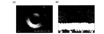
- the amount of metal present in the resin layer 20 is such that when the cross section of the substrate is photographed with a metal microscope, the proportion of metal in the region from the outermost surface of the resin layer 20 to a depth of 0.5 ⁇ m is 5 to 50 area%.
- the arithmetic average roughness Ra JIS B0633-2001
- a multi-layer wiring board having vias and having fine wiring is manufactured through the steps (A) to (F) described above.
- ⁇ Optional step (K): Energy application step> You may provide the process of providing energy with respect to the resin layer 20 arrange
- Examples of the energy application method include exposure processing or heat treatment.
- radiation irradiation can be used.
- the light source include a mercury lamp, a metal halide lamp, a xenon lamp, a chemical lamp, and a carbon arc lamp.
- Examples of radiation include electron beams, X-rays, ion beams, and far infrared rays.
- g-line, i-line, deep-UV light, and high-density energy beam (laser beam) are used.
- a heating method using a thermal recording head or the like, a scanning exposure method using an infrared laser, or the like, and a high-illuminance flash exposure such as a xenon discharge lamp or an infrared lamp exposure are also preferable methods.
- the time required for energy application varies depending on the polymer structure used and the light source, but is usually between 10 seconds and 5 hours.
- the exposure power is in the range of 10 to 10,000 mJ / cm 2 in order to facilitate the graft polymerization and to suppress the decomposition of the produced graft polymer. More preferably, it is in the range of 50 to 7000 mJ / cm 2 .
- step (G) After step (C), a laminated film for forming an adhesion auxiliary layer provided with a temporary support and an adhesion auxiliary layer on the temporary support, and an insulating layer and an insulating layer subjected to desmear treatment on the insulating layer
- the temporary support and the temporary support A laminated film for forming a resin layer comprising a resin layer containing a functional group that forms an interaction with the plating catalyst or its precursor and a polymer containing a polymerizable group on the adhesion auxiliary layer, and a resin layer Lamination so that the adhesion auxiliary layer is in contact, and obtaining a laminate
- step (J) After step (I), the step of peeling the temporary support from the laminate.
- the adhesion assistance layer is insulated. The adhesion between the resin layer and the resin layer is
- a temporary support and a laminated film for forming an adhesion auxiliary layer including an adhesion auxiliary layer on the temporary support are formed on the insulating layer, and the adhesion auxiliary layer and the desmear treatment are performed.
- Lamination is performed so that the applied insulating layer is in contact with each other to obtain a laminate. More specifically, as shown in FIG. 2A, in this step, the adhesion is provided with the temporary support 22 and the adhesion auxiliary layer 30 provided on the temporary support 22 on the insulating layer 16.
- the laminated film 32 for forming the auxiliary layer is laminated so that the adhesion auxiliary layer 30 is in contact with the insulating layer 16 to obtain a laminated body 34.
- the method of laminating the laminated film 32 for forming the adhesion auxiliary layer on the insulating layer 16 so that the adhesion auxiliary layer 30 is in contact with the insulating layer 16 is not particularly limited. Also good.
- the temperature T of the adhesion assisting layer 30 when laminating the adhesion assisting layer forming laminated film 32 is equal to or higher than the glass transition temperature of the adhesion assisting layer as in the above-described condition of the resin layer 20 in the step (D), and the glass transition temperature. + 60 ° C. or lower.
- a preferred embodiment is the same as the resin layer 20 described above.
- the preferable range of the glass transition temperature of the adhesion auxiliary layer 30 is the same as the range of the resin layer 20 described above.
- the Young's modulus of the adhesion assisting layer 30 is 0.16 ⁇ 10 6 to 100 ⁇ 10 6 Pa, similar to the condition of the resin layer 20 in the step (D) described above. A preferable range of Young's modulus is the same as that of the resin layer 20. Furthermore, the elongation at break of the adhesion auxiliary layer 30 is 100% or less, as in the condition of the resin layer 20 in the step (D) described above. A preferable range of elongation at break is the same as that of the resin layer 20.
- a preferable range of the pressure (pressure bonding pressure) P applied to the adhesion auxiliary layer forming laminated film 32 in order to assist adhesion between the adhesion auxiliary layer 30 and the insulating layer 16 during lamination is applied to the resin layer forming laminated film. Same as the pressure range.
- the temperature T of the adhesion assisting layer 30 during lamination the Young's modulus E (T) of the adhesion assisting layer 30 at the temperature T, and the fracture of the adhesion assisting layer 30
- the point P is in the above range, and the pressure P applied to the adhesion auxiliary layer forming laminated film 32 and Log (E (T)) are expressed by the above formulas (I) to (IV) shown in FIG. It exists in the range surrounded by the straight line represented.
- the adhesion auxiliary layer 30 serves to assist the adhesion between the insulating layer 16 and the resin layer 20.
- the adhesion assisting layer 30 gives an active species as a starting point of the binding reaction with the resin layer 20, and can generate a large number of bonds between the adhesion assisting layer 30 and the resin layer 20 from the starting point. For example, it is useful when using a surface graft polymerization method or the like. More specifically, as the adhesion auxiliary layer 30, a layer containing a polymerization initiator (polymerization initiation layer), a layer having a functional group capable of initiating polymerization (polymerization initiation layer), or the like can be used.
- the thickness of the adhesion auxiliary layer 30 is not particularly limited, but is preferably 0.1 to 10 ⁇ m and more preferably 0.2 to 5 ⁇ m from the viewpoint of maintaining film properties and preventing film peeling. In mass after drying is preferably 0.1 ⁇ 20g / m 2, more preferably 0.1 ⁇ 15g / m 2, more preferably 0.1 ⁇ 2g / m 2.
- the method for forming the adhesion assisting layer 30 on the temporary support 22 is not particularly limited, and a known layer forming method such as a coating method, a transfer method, or a printing method is used.
- the adhesion auxiliary layer 30 may be formed by laminating necessary components on the temporary support 22 with an extruder, or a composition containing necessary components may be used.
- a composition the method of immersing the temporary support body 22 in a composition and the method of apply
- the insulating layer 16 formed on the wiring substrate 10 is made of a known insulating resin that has been used as a material for a multilayer laminate, a build-up substrate, or a flexible substrate, it is in close contact with the insulating layer 16.
- a known insulating resin that has been used as a material for a multilayer laminate, a build-up substrate, or a flexible substrate
- an insulating resin composition similar to that used for forming the insulating layer 16 as the resin composition used when forming the adhesion assisting layer 30.
- assistant layer formed from an insulating resin composition is demonstrated.
- the insulating resin composition used when forming the adhesion assisting layer 30 may contain the same electrically insulating resin that constitutes the insulating layer 16 formed on the wiring substrate 10, and is different. However, it is preferable to use materials having similar thermal properties such as glass transition point, elastic modulus, and linear expansion coefficient. Specifically, for example, it is preferable in terms of adhesion to use the same type of insulating resin as the insulating resin constituting the insulating layer 16 formed on the wiring substrate 10. In addition, inorganic or organic particles may be added in order to increase the strength of the adhesion auxiliary layer 30 and to improve electrical characteristics.
- the insulating resin may be, for example, a thermosetting resin, a thermoplastic resin, or a mixture thereof.
- the thermosetting resin include an epoxy resin, a phenol resin, a polyimide resin, a polyester resin, and a bismaleimide. Examples thereof include resins, polyolefin resins, isocyanate resins and the like.
- thermoplastic resin examples include phenoxy resin, polyether sulfone, polysulfone, polyphenylene sulfone, polyphenylene sulfide, polyphenyl ether, polyether imide, and the like.
- the adhesion auxiliary layer 30 may contain a compound having a polymerizable double bond, specifically an acrylate or methacrylate compound, in order to promote crosslinking within the layer, It is preferable to use one.
- the adhesion auxiliary layer 30 can be added with various compounds depending on the purpose as long as the effects of the present invention are not impaired. Specific examples include materials such as rubber and SBR latex that can relieve stress during heating, binders for improving film properties, plasticizers, surfactants, viscosity modifiers, and the like.
- the adhesion auxiliary layer 30 may be filled with a filler (for example, inorganic filler such as silica, alumina, clay, talc, aluminum hydroxide, calcium carbonate, cured epoxy resin, crosslinked benzoguanamine resin, crosslinked acrylic polymer, etc.
- a filler for example, inorganic filler such as silica, alumina, clay, talc, aluminum hydroxide, calcium carbonate, cured epoxy resin, crosslinked benzoguanamine resin, crosslinked acrylic polymer, etc.
- Organic fillers colorants, flame retardants, adhesion-imparting agents, silane coupling agents, antioxidants, ultraviolet absorbers and the like may be added singly or in combination.
- the close adhesion auxiliary layer 30 preferably contains an active species (compound) that generates an active site capable of forming an interaction with the polymer compound constituting the resin layer 20.
- an active species compound
- some energy may be applied, and preferably, light (ultraviolet light, visible light, X-ray, etc.), plasma (oxygen, nitrogen, carbon dioxide, argon, etc.), heat, electricity, Etc. are used.
- active sites may be generated by chemically decomposing the surface with an oxidizing liquid (potassium permanganate solution) or the like.
- the active species include a polymerization initiator (for example, a thermal polymerization initiator, a photopolymerization initiator, a polymer containing a polymerizable group).
- the amount of the polymerization initiator contained in the adhesion auxiliary layer 30 is preferably 0.1 to 50% by mass, and more preferably 1.0 to 30% by mass in terms of solid content.
- a temporary support body is peeled from the laminated body obtained at the process (G). More specifically, as shown in FIG. 2B, in this step, the temporary support 22 is removed from the laminate 34 including the adhesion auxiliary layer forming laminate film 32 deposited on the insulating layer 16. Peel off. By peeling off the temporary support 22, only the adhesion assisting layer 30 in close contact with the insulating layer 16 remains in the laminate, and the adhesion assisting layer 30 disposed on the via hole 18 is laminated with the temporary support 22. Removed from.
- the temperature of the adhesion assisting layer 30 in the step (H) is preferably 0 to 40 ° C., more preferably 10 to 40 ° C., and more preferably 15 to 35, from the point that the excessive adhesion assisting layer 30 is unlikely to remain in the laminate. More preferably.
- the interfacial peel strength ⁇ (B2) between the temporary support 22 and the close-contact auxiliary layer 30 is equal to the interfacial peel strength (A2) between the close-contact auxiliary layer 30 and the insulating layer 16. It is preferably lower than the interfacial peel strength.
- the adhesion assisting layer 30 laminated in a predetermined region may be peeled off from the insulating layer 16 and a transfer failure may occur. Therefore, the above formula (Y) means that the condition for removing the excessive adhesion auxiliary layer 30 overlapping the via hole 18 from the stacked body 34 is satisfied.
- the preferable range of the interfacial peel strength ⁇ (A2) per unit area between the adhesion auxiliary layer 30 and the insulating layer 16 is the same as the preferable range of the interfacial peel strength ⁇ (A1) described above.
- the preferred range of the interfacial peel strength ⁇ (B2) per unit area between the adhesion auxiliary layer 30 and the temporary support 22 is the same as the preferred range of the interfacial peel strength ⁇ (B1) described above.
- the preferable range of the breaking stress ⁇ (C2) of the adhesion auxiliary layer 30 is the same as the preferable range of the breaking stress ⁇ (C1) described above.
- the difference between the interfacial peel strength ⁇ (A2) and the interfacial peel strength ⁇ (B2) is preferably 5 to 50 MPa from the viewpoint that the excessive adhesion assisting layer 30 does not easily remain in the laminate.
- the difference between the interfacial peel strength ⁇ (B2) and the breaking stress ⁇ (C2) is preferably 2 to 10 MPa from the viewpoint that the excessive adhesion assisting layer 30 hardly remains in the laminate.
- a resin layer containing a temporary support, a functional group that interacts with the plating catalyst or its precursor on the temporary support, and a polymer containing a polymerizable group. Is laminated on the adhesion auxiliary layer so that the resin layer and the adhesion auxiliary layer are in contact with each other to obtain a laminate. More specifically, as shown in FIG. 2C, in this step, a resin including a temporary support 22 and a resin layer 20 provided on the temporary support 22 on the adhesion auxiliary layer 30. The layer-forming laminated film 24 is laminated so that the resin layer 20 is in contact with the adhesion auxiliary layer 30 to obtain a laminated body 36.
- the laminated film 24 for forming a resin layer used is as described above.
- the conditions for laminating are also the same as in the above step (D), and the preferred embodiment is also the same.
- a temporary support body is peeled from the laminated body obtained at the process (I). More specifically, as shown in FIG. 2D, in this step, from the laminate 36 including the resin layer forming laminated film 24 deposited on the adhesion auxiliary layer 30 in the step (J), The temporary support 22 is peeled off. By peeling off the temporary support 22, only the resin layer 20 in close contact with the adhesion auxiliary layer 30 remains in the laminate, and the resin layer 20 disposed on the via hole 18 is removed from the laminate 36 together with the temporary support 22. Removed.
- the temperature of the resin layer 20 in the step (J) is preferably 0 to 40 ° C., more preferably 10 to 40 ° C., and more preferably 15 to 35 ° C. from the point that the excess resin layer 20 hardly remains in the laminate. Further preferred.
- the interface peel strength ⁇ (A3) per unit area between the resin layer 20 and the adhesion auxiliary layer 30 is expressed by the following formula (Z). It is preferable to satisfy the relationship.
- the interfacial peel strength ⁇ (A3) per unit area of the adhesion assisting layer 30 and the adhesion assisting layer 30 is preferably 30 to 500 MPa, and more preferably 40 to 300 MPa.
- the step (F) is performed to form a conductive metal film 28 in contact with the metal wiring 14 as shown in FIG. 2 (E).
- the multilayer wiring board obtained by the above-described manufacturing method can also be used as a board serving as a core for forming further wiring so as to be suitable for mounting.
- a known semi-additive method, subtractive method, or the like can be appropriately applied. For example, first, a resist film is provided on the obtained multilayer wiring board, pattern exposure is performed, and development processing is performed to produce a pattern resist film. Thereafter, using the patterned resist film as a mask, a quick etching process is performed to remove the metal film in the non-pattern region, and then the patterned resist film is removed.
- the multilayer wiring board obtained by the present invention can be applied to various uses such as a semiconductor chip, various electric wiring boards, FPC, COF, TAB, motherboard, package interposer board, and the like.
- the multilayer wiring board produced by the method of the present invention can easily form wiring with excellent adhesion to a smooth substrate, has good high-frequency characteristics, and is a fine high-density wiring. Excellent connection reliability between wires.
- the acid value of the obtained polymer B was measured using a potentiometric automatic titrator (manufactured by Kyoto Electronics Industry Co., Ltd.) and a 0.1 M sodium hydroxide aqueous solution as the titrant, the acid value of the polymer B was 3 0.2 mmol / g.
- the obtained polymer B was identified using an IR measuring machine (manufactured by Horiba, Ltd.). The measurement was performed by dissolving the polymer in acetone and using KBr crystals. As a result of IR measurement, a peak was observed around 2240 cm ⁇ 1 , and it was found that acrylonitrile, which is a nitrile unit, was introduced into the polymer. Moreover, it turned out that acrylic acid is introduce
- DMSO dimethyl sulfoxide
- Step (X) A double-sided copper-clad plate (glass epoxy substrate) was CZ-treated (trade name: CZ-8100, manufactured by MEC Co., Ltd.) to finely roughen the copper surface.
- a dry film resist (DFR, trade name: RY3315, manufactured by Hitachi Chemical Co., Ltd.) was laminated on the finely roughened copper surface with a vacuum laminator at a pressure of 0.2 MPa at 70 ° C. After lamination, the copper pattern forming portion was subjected to mask exposure with an exposure machine having a central wavelength of 365 nm under the condition of 70 mJ / m 2 . Thereafter, development was performed with a 1% aqueous sodium bicarbonate solution, followed by washing with water to obtain a resist pattern for subtractive etching.
- DFR dry film resist
- Step (Z) Next, a 40% cupric oxide solution at 45 ° C. was sprayed onto the obtained substrate until the copper in the non-resist portion where the resist pattern was not formed was etched. Thereafter, the obtained substrate was washed with water.
- Step (W) Next, in order to remove the resist pattern, the substrate was immersed in a 4% NaOH aqueous solution at 45 ° C. for 60 seconds. Thereafter, the obtained substrate was washed with water and immersed in 1% sulfuric acid for 30 seconds. Thereafter, it was washed again with water.
- an epoxy insulating film GX-13 (film thickness 40 ⁇ m) manufactured by Ajinomoto Fine-Techno Co., Ltd. is used as an electrical insulating layer on the substrate obtained in the step (W), and 100 to 110 at a pressure of 0.2 MPa using a vacuum laminator.
- the insulating film was formed by bonding under the condition of ° C. Thereafter, heat treatment was performed at 180 ° C. for 30 minutes.
- Step (B) A via hole reaching the copper foil having a top diameter of 60 ⁇ m and a bottom diameter of 50 ⁇ m was formed at a predetermined position on the insulating layer obtained in the step (A) by a CO 2 laser.
- the neutralization process was performed by immersing for 5 minutes at 45 degreeC, adding stirring using the neutralization aqueous solution containing a sulfuric acid.
- the insulating layer residue at the bottom of the via hole was removed. This was confirmed by the BSE image (reflection electron image) by the surface SEM.
- the surface roughness (Ra) of the insulating layer after the desmear treatment was 0.8 ⁇ m.
- the laminated film for resin layer formation used at a process (D) was produced with the following method.
- Polymer A 10.5 parts by mass, 73.3 parts by mass of acetone, 33.9 parts by mass of methanol, and 4.8 parts by mass of N, N-dimethylacetamide were mixed and stirred to prepare a coating solution.
- the prepared coating solution is applied by spin coating onto a PET support having a film thickness of 32 ⁇ m by a spin coating method, dried at 80 ° C. for 20 minutes, and a resin layer having a resin layer having a thickness of 0.5 ⁇ m A laminated film for formation was obtained.
- the obtained laminated film was laminated on the insulating layer having the via hole obtained in the step (C) while applying a predetermined pressure (pressing) to obtain a laminated body.
- the pressure condition at the time of lamination is either 0.1 MPa, 0.2 MPa, 0.4 MPa, 0.7 MPa, or 1.0 MPa.
- the temperature of the resin layer in the case of lamination is either 60 degreeC, 90 degreeC, 120 degreeC, or 150 degreeC.
- the time for applying pressure (pressing time) was 30 seconds.
- Step (E) The resin layer in the laminate obtained in the step (D) was cooled to room temperature (25 ° C.), and the PET support as a temporary support was peeled from the laminate. In the obtained laminate, a resin layer was deposited only on the insulating layer. In addition, after this process, a surface inspection was performed with an optical microscope, and it was inspected whether there was a transfer defect of the sheet product or a resin layer in a portion overlapping with the via hole was not cut out. In the inspection, only the sample having no problem was subjected to the following steps.
- Step (K) A UV exposure machine (model number: UVF-502S, lamp: UXM-501MD) manufactured by Mitsunaga Electric was used for the obtained laminate, and an irradiation power of 1.5 mW / cm 2 (ultraviolet integrated light meter manufactured by Ushio Electric Co., Ltd.).
- the irradiation polymer was irradiated with UV light of 254 nm at 500 mJ using a UIT150-light receiving sensor UVD-S254, and a graft polymer was formed on the entire surface of the insulating layer.
- the obtained laminate was immersed in stirred acetone for 5 minutes, and then washed with distilled water. As described above, a resin layer chemically bonded directly to the insulating layer was formed.
- Step (F) A palladium catalyst comprising 40 parts by mass of diethylene glycol diethyl ether (manufactured by Wako Pure Chemical Industries, Ltd.), 40 parts by mass of water, 20 parts by mass of nitric acid (manufactured by Wako Pure Chemical Industries, Ltd.), and 0.25 parts by mass of palladium acetate (manufactured by Wako Pure Chemical Industries, Ltd.) A solution was prepared, and the laminate obtained in step (K) was immersed in this palladium catalyst solution for 5 minutes, and then washed with water.
- an electroless plating bath having the following composition using Sulcup PGT (PGT-A, PGT-B, PGT-C) manufactured by Uemura Kogyo Co., Ltd. was used for the laminate provided with the plating catalyst. Electroless plating was performed at an electroless plating temperature of 26 ° C. for 30 minutes. The thickness of the obtained electroless copper plating film was 0.5 ⁇ m both on the resin layer, on the side surface of the via hole, and on the bottom.
- the raw materials for the electroless plating solution are as follows.
- the obtained laminate with electroless copper plating film was heat-treated at 150 ° C. for 30 minutes, and then degreased with 10% sulfuric acid in order to remove the heat-treated oxide film.
- An electroplating solution was prepared with the following raw material composition using CU-BRITE VFII-A and CU-BRITE VFII-B manufactured by EBARA Eugene Light Co., Ltd., and a laminate to which electroless copper plating was applied using the electroplating solution On the other hand, electroplating for 40 minutes was performed.
- the current value at the time of electroplating was 0.3 A / dm 2.
- the thickness of the obtained electrolytic copper plating film was 25 ⁇ m on the insulating film and 50 ⁇ m on the bottom of the via hole.
- FIG. 8A is a schematic cross-sectional view showing the via chain obtained in the first embodiment.
- Example 2 A multilayer wiring board and a via chain were produced in the same manner as in Example 1 except that the thickness of the resin layer was changed from 0.5 ⁇ m to 2.5 ⁇ m in the step (D).
- a schematic cross-sectional view of the via chain obtained in Example 2 is shown in FIG.
- Example 3 The same method as in Example 1 except that in the step (D), the polymer B was used instead of the polymer A, and in the step (F), a 0.5 mass% silver nitrate aqueous solution was used instead of the palladium catalyst solution. Thus, a multilayer wiring board and a via chain were produced. A schematic cross-sectional view of the via chain obtained in Example 3 is shown in FIG.
- Example 4 Before the step (D) of Example 1, the following step (G) and step (H) are carried out, and then the laminated body provided with the obtained adhesion auxiliary layer is the step of Example 1. Steps (F) to (F) were carried out to produce a multilayer wiring board and a via chain having an adhesion auxiliary layer and a resin layer.
- FIG. 8B is a schematic cross-sectional view showing the via chain obtained in Example 4, and includes an adhesion auxiliary layer as compared with FIG. 8A.
- Step (G) First, the adhesion auxiliary layer forming laminated film used in the step (G) was produced by the following method.
- the prepared coating solution is applied by spin coating onto a PET support having a film thickness of 32 ⁇ m by a spin coating method, dried at 80 ° C. for 20 minutes, and provided with an adhesion auxiliary layer having a thickness of 1.5 ⁇ m.
- a laminated film for forming an auxiliary layer was obtained.
- the obtained laminated film was laminated on the insulating layer having the via hole obtained in the step (C) while applying a predetermined pressure (pressing) to obtain a laminated body.
- the pressure condition at the time of lamination is either 0.1 MPa, 0.2 MPa, 0.4 MPa, 0.7 MPa, or 1.0 MPa.
- the temperature of the adhesion auxiliary layer at the time of laminating is either 60 ° C., 90 ° C., 120 ° C., or 150 ° C.
- the time for applying pressure (pressing time) was 30 seconds.
- Step (H) The adhesion auxiliary layer in the laminate obtained in the step (G) was cooled to room temperature (25 ° C.), and the PET support as a temporary support was peeled from the laminate. In the obtained laminate, the adhesion auxiliary layer was deposited only on the insulating layer. After the step, a surface inspection was performed with an optical microscope, and it was inspected whether there was a transfer defect of the sheet product or whether the adhesion assisting layer in the portion overlapping with the via hole was cut out. In the inspection, only the sample having no problem was subjected to the step (D).
- Example 1 Using the materials used in Example 1 described in paragraphs [0121] to [0133] of JP 2010-157590 A, the same method as in Examples 1 to 3 described above was used. A multilayer wiring board having a structure was prepared. Further, steps (Y) to (W) are performed on the obtained multilayer wiring board in the same manner as in Examples 1 to 3, and 100 blind vias of 50 ⁇ m ⁇ as shown in FIG. 8A are connected. 10 units of via chains were formed.
- the resin layer (hereinafter referred to as resin layer A) composed of the polymer A used above, the resin layer composed of polymer B (hereinafter referred to as resin layer B as appropriate), and the Young's modulus (storage elastic modulus) of the adhesion auxiliary layer It measured with the frequency of 1 Hz with the dynamic viscoelasticity measuring apparatus (DMS6100, product made from SII).
- the glass transition temperature of the resin layer A is 35 ° C.
- the Young's modulus in the temperature range of glass transition temperature to glass transition temperature + 60 ° C. is 2.0 ⁇ 10 5 to 6.0 ⁇ 10 7 MPa, and the breaking point The elongation was 70%.
- the resin layer B has a glass transition temperature of 75 ° C., and a Young's modulus in the temperature range of glass transition temperature to glass transition temperature + 60 ° C. is 5.0 ⁇ 10 5 to 1.0 ⁇ 10 8 MPa, The elongation was 25%.
- the adhesion assisting layer has a glass transition temperature of 105 ° C., and a Young's modulus in the temperature range of glass transition temperature to glass transition temperature + 60 ° C. is 8.0 ⁇ 10 5 to 1.0 ⁇ 10 8 MPa. The elongation was 15%.
- Example 3 the interfacial peel strength ⁇ (A1) per unit area between the resin layer B and the insulating layer is 220 MPa, and the interfacial peel strength ⁇ (B1) per unit area between the resin layer B and the temporary support is 160 MPa.
- the breaking stress ⁇ (C1) of the resin layer B was 100 MPa, and the relationship of ⁇ (A1)> ⁇ (B1)> ⁇ (C1) was satisfied.
- Example 4 the interfacial peel strength ⁇ (A2) per unit area of the adhesion auxiliary layer and the insulating layer is 180 MPa, and the interfacial peel strength ⁇ (B2) per unit area of the adhesion auxiliary layer and the temporary support is 130 MPa, The breaking stress ⁇ (C2) of the adhesion auxiliary layer was 80 MPa, and the relationship of ⁇ (A2)> ⁇ (B2)> ⁇ (C2) was satisfied.
- the interfacial peel strength ⁇ (A3) per unit area between the resin layer A and the adhesion auxiliary layer is 180 MPa, and the interfacial peel strength ⁇ (B1) per unit area between the resin layer A and the temporary support. Is 130 MPa, the breaking stress ⁇ (C1) of the resin layer A is 80 MPa, and ⁇ (A2), ⁇ (A3)> ⁇ (B1), ⁇ (B2)> ⁇ (C1), ⁇ (C2) was met.
- Example 1 to Example 4 the yield of the unnecessary area cut-off removal of the sheet that overlaps the via hole after the temporary support peeling in the step (D) or the step (H) is obtained as a resin layer A, a resin layer B, Each adhesion auxiliary layer was examined. Specifically, as shown in the Examples, lamination of each laminated film was performed under a total of 20 conditions of a combination of 4 temperatures and 5 press points. The number of inspected via holes was 441 each, and the inspection was performed by observing the surface of the laminate after peeling off the temporary support with an electron microscope.
- the number of via holes remaining without being blocked by the resin layer A, the resin layer B, or the adhesion auxiliary layer is counted, and the cut-off removal rate ( The remaining via hole / 441) was calculated. The higher the cutout removal rate, the more via holes remain.
- the one with a cut-off removal rate of 100% is judged as ⁇ , the one with 20% or more but less than 100% is judged as ⁇ , the one with less than 20% is judged as ⁇ , the Young's modulus (storage modulus) of the sheet product at the laminating temperature, and the laminating pressure Mapping was done for.
- the results of Examples 1 to 4 are shown in Table 1, and the results of mapping are shown in Table 7.
- Example 4 in Table 1 is a result of measuring the cut-off removal rate of the adhesion auxiliary layer using the laminated film for forming the adhesion auxiliary layer.
- the result of the cutout removal rate of the resin layer in Example 4 was the same as that in Example 1.
- FIG. 4 shows an SEM photograph of an OK product (via holes remain)
- FIG. 5 and FIG. 6 show an SEM photograph of an NG product (via holes blocked by various layers).
- FIG. 5 shows a case where a part of each layer remains
- FIG. 6 shows a case where the via hole is blocked by each layer.
- Example 4 in Table 2 the cutout removal rate of the resin layer A and the adhesion auxiliary layer was 100%. It was found that vias formed by the manufacturing method of the present invention have very good via chain conduction compared to the comparative example. On the other hand, when the defective conduction of the failed product of the comparative example was examined, it was found that many filling defects as shown in the SEM photograph of FIG. 9 occurred frequently. In the comparative example, it was found from the SEM photograph that the plating growth from the wall surface was low or unstable. This can be expected to be caused by forming the resin layer using the liquid composition.
- Wiring substrate 12 Substrate 14: Metal wiring 16: Insulating layer 18: Via hole 20: Resin layer 22: Temporary support 24: Laminate film 26, 34, 36 for resin layer formation: Laminate 28: Metal film 30: Adhesion Auxiliary layer 32: laminated film for adhesion auxiliary layer
Landscapes
- Engineering & Computer Science (AREA)
- Manufacturing & Machinery (AREA)
- Microelectronics & Electronic Packaging (AREA)
- Production Of Multi-Layered Print Wiring Board (AREA)
- Manufacturing Of Printed Wiring (AREA)
Abstract
本発明は、高精細かつ密着性に優れた金属配線を製造できると共に、ビアの接続信頼性に優れた多層配線基板を、高歩留まりで製造することができる、生産性に優れた多層配線基板の製造方法を提供することを目的とする。本発明の多層配線基板の製造方法は、(A)金属配線を備える配線基板の表面に、絶縁層を形成する工程と、(B)ビアホールを形成する工程と、(C)デスミア処理を行う工程と、(D)仮支持体と、仮支持体上にめっき触媒またはその前駆体と相互作用を形成する官能基、及び、重合性基を含有するポリマーを含む樹脂層とを備える樹脂層形成用積層フィルムを、絶縁層上に、樹脂層とデスミア処理が施された絶縁層とが接するようにラミネートし、積層体を得る工程と、(E)積層体から仮支持体を剥離する工程と、(F)ビアホールの壁面および樹脂層にめっき触媒またはその前駆体を付与し、めっきを行う工程と、を備える。
Description
本発明は、多層配線基板の製造方法に関する。
近年、電子機器の高機能化等の要求に伴い、電子部品の高密度集積化、更には高密度実装化等が進んでおり、これらに使用される高密度実装対応のプリント配線板等も小型化かつ高密度化が進んでいる。このプリント配線板等の高密度化への対応としては、高精細で安定な配線の実現やビルドアップ多層配線板の採用などの方法が種々検討されている。更に、微細なビアにより電気的絶縁層間を接続された、ビルドアップ法により配線層を積層してなる製品も出されている。
現在まで、様々な多層配線板に関する製造方法が提案されている(特許文献1~4)。
なかでも、特許文献4には、ビアによる層間接続がなされ、且つ、微細配線を有する多層配線基板を簡便な方法で製造することが可能な多層配線基板の製造方法が提案されている。
該方法においては、具体的には、まず、電気導通可能な部位を有する基板の表面に、絶縁層を形成し、次に、絶縁層をレーザ又はドリルにより部分的に除去し、ビアホールを形成する。その後、ビアホールが形成された面に対してデスミア処理を行い、ビアホールの底部における前記絶縁層の残渣を除去する。さらに、デスミア処理が行われた面上に、所定の官能基を有する樹脂を含む液状組成物を用いて樹脂層を形成する。その後、ビアホールの底部に形成された樹脂層を、処理液を付与して除去して、残存する樹脂層に対してめっき触媒を付与した後、めっきを行う。
なかでも、特許文献4には、ビアによる層間接続がなされ、且つ、微細配線を有する多層配線基板を簡便な方法で製造することが可能な多層配線基板の製造方法が提案されている。
該方法においては、具体的には、まず、電気導通可能な部位を有する基板の表面に、絶縁層を形成し、次に、絶縁層をレーザ又はドリルにより部分的に除去し、ビアホールを形成する。その後、ビアホールが形成された面に対してデスミア処理を行い、ビアホールの底部における前記絶縁層の残渣を除去する。さらに、デスミア処理が行われた面上に、所定の官能基を有する樹脂を含む液状組成物を用いて樹脂層を形成する。その後、ビアホールの底部に形成された樹脂層を、処理液を付与して除去して、残存する樹脂層に対してめっき触媒を付与した後、めっきを行う。
特許文献4に方法においては、上述したように、ビアホールが形成された絶縁層上に、液状組成物を用いて樹脂層を形成している。その際、該液状組成物はビアホール内部まで侵入するため、ビアホール内部にたまった不要な樹脂は除去する必要がある。
しかしながら、ビアホール底面の樹脂の除去を行いつつ、ビアホール壁面の樹脂の付着状態を制御することは工業的なレベルでは非常に困難であり、結果、ビアめっき不良やビア形状のバラツキを招きやすい。実際、本発明者らが、特許文献4に記載の方法を利用して多層配線基板の製造を行ったところ、初期導通不良が起きやすく、昨今要求される歩留まりレベルには到達しておらず、さらなる改良が必要であった。
しかしながら、ビアホール底面の樹脂の除去を行いつつ、ビアホール壁面の樹脂の付着状態を制御することは工業的なレベルでは非常に困難であり、結果、ビアめっき不良やビア形状のバラツキを招きやすい。実際、本発明者らが、特許文献4に記載の方法を利用して多層配線基板の製造を行ったところ、初期導通不良が起きやすく、昨今要求される歩留まりレベルには到達しておらず、さらなる改良が必要であった。
本発明は、上記実情を鑑みて、高精細かつ密着性に優れた金属配線を製造できると共に、ビアの接続信頼性に優れた多層配線基板を、高歩留まりで製造することができる、生産性に優れた多層配線基板の製造方法を提供することを目的とする。
本発明者は、上記課題に鑑みて鋭意検討した結果、以下に示す手段により上記目的を達
成しうることを見出した。
成しうることを見出した。
(1) (A)金属配線を備える配線基板の表面に、絶縁層を形成する工程と
(B)前記絶縁層を貫通し、前記金属配線に達するようにビアホールを形成する工程と、
(C)前記工程(B)後に、デスミア処理を行う工程と、
(D)前記工程(C)後に、仮支持体と、前記仮支持体上にめっき触媒またはその前駆体と相互作用を形成する官能基、及び、重合性基を含有するポリマーを含む樹脂層とを備える樹脂層形成用積層フィルムを、前記絶縁層上に、前記樹脂層とデスミア処理が施された前記絶縁層とが接するようにラミネートし、積層体を得る工程と、
(E)前記工程(D)後に、前記積層体から前記仮支持体を剥離する工程と、
(F)前記工程(E)後に、前記ビアホールの壁面および前記樹脂層にめっき触媒またはその前駆体を付与し、めっきを行う工程と、を備え、
前記工程(D)において、ラミネートする際の前記樹脂層の温度Tが、前記樹脂層のガラス転移温度以上ガラス転移温度+60℃以下であり、前記温度Tにおける前記樹脂層のヤング率E(T)が0.16×10⁶~100×106Paで、前記樹脂層の破断点伸度が100%以下であり、
前記樹脂層形成用積層フィルムをラミネートする際に、前記樹脂層形成用積層フィルムに加えられる圧力Pと、Log(E(T))とが、図3に示される、下記式(I)~(IV)で表される直線で囲まれた範囲に存在する、多層配線基板の製造方法。
式(I) Log(E(T))=5.2
式(II) Log(E(T))=8
式(III) P=0.3×10⁶(Log(E(T))-1.4×10⁶
式(IV) P=0.06×10⁶(Log(E(T))-0.3×10⁶
(B)前記絶縁層を貫通し、前記金属配線に達するようにビアホールを形成する工程と、
(C)前記工程(B)後に、デスミア処理を行う工程と、
(D)前記工程(C)後に、仮支持体と、前記仮支持体上にめっき触媒またはその前駆体と相互作用を形成する官能基、及び、重合性基を含有するポリマーを含む樹脂層とを備える樹脂層形成用積層フィルムを、前記絶縁層上に、前記樹脂層とデスミア処理が施された前記絶縁層とが接するようにラミネートし、積層体を得る工程と、
(E)前記工程(D)後に、前記積層体から前記仮支持体を剥離する工程と、
(F)前記工程(E)後に、前記ビアホールの壁面および前記樹脂層にめっき触媒またはその前駆体を付与し、めっきを行う工程と、を備え、
前記工程(D)において、ラミネートする際の前記樹脂層の温度Tが、前記樹脂層のガラス転移温度以上ガラス転移温度+60℃以下であり、前記温度Tにおける前記樹脂層のヤング率E(T)が0.16×10⁶~100×106Paで、前記樹脂層の破断点伸度が100%以下であり、
前記樹脂層形成用積層フィルムをラミネートする際に、前記樹脂層形成用積層フィルムに加えられる圧力Pと、Log(E(T))とが、図3に示される、下記式(I)~(IV)で表される直線で囲まれた範囲に存在する、多層配線基板の製造方法。
式(I) Log(E(T))=5.2
式(II) Log(E(T))=8
式(III) P=0.3×10⁶(Log(E(T))-1.4×10⁶
式(IV) P=0.06×10⁶(Log(E(T))-0.3×10⁶
(2) 前記工程(E)において、前記樹脂層の温度が0~40℃であり、
前記樹脂層と前記絶縁層との単位面積当たりの界面剥離強度σ(A1)と、前記樹脂層と前記仮支持体との単位面積当たりの界面剥離強度σ(B1)と、前記樹脂層の破断応力σ(C1)とが、以下の関係を満足する、(1)に記載の多層配線基板の製造方法。
σ(A1)>σ(B1)>σ(C1)
(3) 前記樹脂層の厚みが、0.05~3.0μmである、(1)または(2)に記載の多層配線基板の製造方法。
(4) 前記工程(E)と前記工程(F)との間に、前記樹脂層に対してエネルギー付与を行う工程を備える、(1)~(3)のいずれかに記載の多層配線基板の製造方法。
前記樹脂層と前記絶縁層との単位面積当たりの界面剥離強度σ(A1)と、前記樹脂層と前記仮支持体との単位面積当たりの界面剥離強度σ(B1)と、前記樹脂層の破断応力σ(C1)とが、以下の関係を満足する、(1)に記載の多層配線基板の製造方法。
σ(A1)>σ(B1)>σ(C1)
(3) 前記樹脂層の厚みが、0.05~3.0μmである、(1)または(2)に記載の多層配線基板の製造方法。
(4) 前記工程(E)と前記工程(F)との間に、前記樹脂層に対してエネルギー付与を行う工程を備える、(1)~(3)のいずれかに記載の多層配線基板の製造方法。
(5) 前記工程(D)および前記工程(E)の代わりに、以下の工程(G)から工程(J)をこの順に実施する、(1)に記載の多層配線基板の製造方法。
(G)前記工程(C)後に、仮支持体と、前記仮支持体上に密着補助層とを備える密着補助層形成用積層フィルムを、前記絶縁層上に、前記密着補助層とデスミア処理が施された前記絶縁層とが接するようにラミネートし、積層体を得る工程
(H)前記工程(G)後に、前記積層体から前記仮支持体を剥離する工程
(I)前記工程(H)後に、仮支持体と、前記仮支持体上にめっき触媒またはその前駆体と相互作用を形成する官能基、及び、重合性基を含有するポリマーを含む樹脂層とを備える樹脂層形成用積層フィルムを、前記密着補助層上に、前記樹脂層と前記密着補助層とが接するようにラミネートし、積層体を得る工程
(J)前記工程(I)後に、前記積層体から前記仮支持体を剥離する工程
なお、前記工程(G)および前記工程(I)において、ラミネートする際の前記密着補助層および前記樹脂層の温度Tが、前記密着補助層および前記樹脂層のそれぞれのガラス転移温度以上ガラス転移温度+60℃以下であり、前記温度Tにおける前記密着補助層および前記樹脂層のヤング率E(T)が0.16×10⁶~100×106Paで、前記密着補助層および前記樹脂層の破断点伸度が100%以下であり、
前記密着補助層形成用積層フィルムおよび前記樹脂層形成用積層フィルムをラミネートする際に、前記密着補助層形成用積層フィルムおよび前記樹脂層形成用積層フィルムに加えられる圧力Pと、Log(E(T))とが、図3に示される、下記式(I)~(IV)で表される直線で囲まれた範囲に存在する。
式(I) Log(E(T))=5.2
式(II) Log(E(T))=8
式(III) P=0.3×10⁶(Log(E(T))-1.4×10⁶
式(IV) P=0.06×10⁶(Log(E(T))-0.3×10⁶
(G)前記工程(C)後に、仮支持体と、前記仮支持体上に密着補助層とを備える密着補助層形成用積層フィルムを、前記絶縁層上に、前記密着補助層とデスミア処理が施された前記絶縁層とが接するようにラミネートし、積層体を得る工程
(H)前記工程(G)後に、前記積層体から前記仮支持体を剥離する工程
(I)前記工程(H)後に、仮支持体と、前記仮支持体上にめっき触媒またはその前駆体と相互作用を形成する官能基、及び、重合性基を含有するポリマーを含む樹脂層とを備える樹脂層形成用積層フィルムを、前記密着補助層上に、前記樹脂層と前記密着補助層とが接するようにラミネートし、積層体を得る工程
(J)前記工程(I)後に、前記積層体から前記仮支持体を剥離する工程
なお、前記工程(G)および前記工程(I)において、ラミネートする際の前記密着補助層および前記樹脂層の温度Tが、前記密着補助層および前記樹脂層のそれぞれのガラス転移温度以上ガラス転移温度+60℃以下であり、前記温度Tにおける前記密着補助層および前記樹脂層のヤング率E(T)が0.16×10⁶~100×106Paで、前記密着補助層および前記樹脂層の破断点伸度が100%以下であり、
前記密着補助層形成用積層フィルムおよび前記樹脂層形成用積層フィルムをラミネートする際に、前記密着補助層形成用積層フィルムおよび前記樹脂層形成用積層フィルムに加えられる圧力Pと、Log(E(T))とが、図3に示される、下記式(I)~(IV)で表される直線で囲まれた範囲に存在する。
式(I) Log(E(T))=5.2
式(II) Log(E(T))=8
式(III) P=0.3×10⁶(Log(E(T))-1.4×10⁶
式(IV) P=0.06×10⁶(Log(E(T))-0.3×10⁶
(6) 前記工程(J)と前記工程(F)との間に、前記樹脂層に対してエネルギー付与を行う工程を備える、(5)に記載の多層配線基板の製造方法。
(7) 前記密着補助層が重合開始剤を含有する、(5)または(6)に記載の多層配線基板の製造方法。
(8) 前記めっき触媒またはその前駆体が、Pd、Ag、またはCuを含む化合物である、(1)~(7)のいずれかに記載の多層配線基板の製造方法。
(9) 前記めっき触媒またはその前駆体と相互作用を形成する官能基が、シアノ基またはカルボン酸基である、(1)~(8)のいずれかに記載の多層配線基板の製造方法。
(10) (1)~(9)のいずれかに記載の多層配線基板の製造方法によって得られる多層配線基板。
(7) 前記密着補助層が重合開始剤を含有する、(5)または(6)に記載の多層配線基板の製造方法。
(8) 前記めっき触媒またはその前駆体が、Pd、Ag、またはCuを含む化合物である、(1)~(7)のいずれかに記載の多層配線基板の製造方法。
(9) 前記めっき触媒またはその前駆体と相互作用を形成する官能基が、シアノ基またはカルボン酸基である、(1)~(8)のいずれかに記載の多層配線基板の製造方法。
(10) (1)~(9)のいずれかに記載の多層配線基板の製造方法によって得られる多層配線基板。
本発明によれば、高精細かつ密着性に優れた金属配線を製造できると共に、ビアの接続信頼性に優れた多層配線基板を、高歩留まりで製造することができる、生産性に優れた多層配線基板の製造方法を提供することができる。
以下に、本発明の多層配線基板の製造方法について詳述する。
本発明の製造方法の特徴点の一つは、ビアホールが形成された絶縁層上に、仮支持体と樹脂層とを備える樹脂層形成用積層フィルムを配置し、その後、仮支持体を剥離することにある。該手順において、仮支持体を積層体から剥離する際に、ビアホールの外周位置において応力集中が生じるため、ビアホールの外周形状に沿った形で樹脂層の切断が生じる。その結果、絶縁層と密着していない仮支持体上の樹脂層はそのまま仮支持体上に残存して、仮支持体の剥離と共に積層体から除去され、実質的に絶縁層上にのみ樹脂層を形成することができる。このようにして得られた基板を使用すると、ビアの接続信頼性に優れた多層配線基板を生産性よく製造することができる。また、該方法では、有機溶媒などを含んだ液状組成物を使用しないため、環境面およびプロセス面からも優れた方法と言える。
本発明の製造方法の特徴点の一つは、ビアホールが形成された絶縁層上に、仮支持体と樹脂層とを備える樹脂層形成用積層フィルムを配置し、その後、仮支持体を剥離することにある。該手順において、仮支持体を積層体から剥離する際に、ビアホールの外周位置において応力集中が生じるため、ビアホールの外周形状に沿った形で樹脂層の切断が生じる。その結果、絶縁層と密着していない仮支持体上の樹脂層はそのまま仮支持体上に残存して、仮支持体の剥離と共に積層体から除去され、実質的に絶縁層上にのみ樹脂層を形成することができる。このようにして得られた基板を使用すると、ビアの接続信頼性に優れた多層配線基板を生産性よく製造することができる。また、該方法では、有機溶媒などを含んだ液状組成物を使用しないため、環境面およびプロセス面からも優れた方法と言える。
該製造方法は、以下の6つの工程を備える。
(A)金属配線を備える配線基板の表面に、絶縁層を形成する工程
(B)上記絶縁層を貫通し、金属配線に達するようにビアホールを形成する工程
(C)上記工程(B)後に、デスミア処理を行う工程
(D)上記工程(C)後に、仮支持体と、仮支持体上にめっき触媒またはその前駆体と相互作用を形成する官能基、及び、重合性基を含有するポリマーを含む樹脂層とを備える樹脂層形成用積層フィルムを、絶縁層上に、樹脂層とデスミア処理が施された絶縁層とが接するようにラミネートし、積層体を得る工程
(E)上記工程(D)後に、積層体から仮支持体を剥離する工程
(F)上記工程(E)後に、ビアホールの壁面および樹脂層にめっき触媒またはその前駆体を付与し、めっきを行う工程
以下に、図面を参照して、各工程を順次に説明する。
(A)金属配線を備える配線基板の表面に、絶縁層を形成する工程
(B)上記絶縁層を貫通し、金属配線に達するようにビアホールを形成する工程
(C)上記工程(B)後に、デスミア処理を行う工程
(D)上記工程(C)後に、仮支持体と、仮支持体上にめっき触媒またはその前駆体と相互作用を形成する官能基、及び、重合性基を含有するポリマーを含む樹脂層とを備える樹脂層形成用積層フィルムを、絶縁層上に、樹脂層とデスミア処理が施された絶縁層とが接するようにラミネートし、積層体を得る工程
(E)上記工程(D)後に、積層体から仮支持体を剥離する工程
(F)上記工程(E)後に、ビアホールの壁面および樹脂層にめっき触媒またはその前駆体を付与し、めっきを行う工程
以下に、図面を参照して、各工程を順次に説明する。
<工程(A):絶縁層形成工程>
工程(A)では、金属配線を備える配線基板の表面に、絶縁層を形成する。
より具体的には、図1(A)に示されるように、本工程においては、基板12に金属配線14が形成された配線基板10と、配線基板10上に設けられた絶縁層16とを備える積層体が形成される。
以下に、配線基板10、および絶縁層16に関して詳述する。
工程(A)では、金属配線を備える配線基板の表面に、絶縁層を形成する。
より具体的には、図1(A)に示されるように、本工程においては、基板12に金属配線14が形成された配線基板10と、配線基板10上に設けられた絶縁層16とを備える積層体が形成される。
以下に、配線基板10、および絶縁層16に関して詳述する。
<配線基板10>
本発明に用いられる配線基板10は、例えば、基板12の片面又は両面に金属配線14を有するものであればよい。また、金属配線14は、図1に示されるように、基板の表面に対してパターン状に形成されていてもよいし、全面に形成されていてもよい。代表的には、エッチング処理を利用したサブストラクティブ法で形成されたものや、電解めっきを利用したセミアディティブ法で形成したものが挙げられ、いずれの工法で形成されたものを用いてもよい。
配線基板10としては、より具体的には、両面又は片面の銅張積層板(CCL)や、この銅張積層板の銅膜をパターン状にしたもの等が用いられ、これらはフレキシブル基板であってもよいし、リジット基板であってもよい。
本発明に用いられる配線基板10は、例えば、基板12の片面又は両面に金属配線14を有するものであればよい。また、金属配線14は、図1に示されるように、基板の表面に対してパターン状に形成されていてもよいし、全面に形成されていてもよい。代表的には、エッチング処理を利用したサブストラクティブ法で形成されたものや、電解めっきを利用したセミアディティブ法で形成したものが挙げられ、いずれの工法で形成されたものを用いてもよい。
配線基板10としては、より具体的には、両面又は片面の銅張積層板(CCL)や、この銅張積層板の銅膜をパターン状にしたもの等が用いられ、これらはフレキシブル基板であってもよいし、リジット基板であってもよい。
より具体的には、リジット基板においては、紙基材銅張積層板として、紙・フェノール樹脂銅張積層板(FR-1、FR-2、XXXPc、XPc)、紙・エポキシ樹脂銅張積層板(FR-3)、紙・ポリエステル銅張積層板が挙げられ、ガラス基材銅張積層板として、ガラス布・エポキシ樹脂銅張積層板(FR-4、G10)、耐熱ガラス布・エポキシ樹脂銅張積層板(FR-5、G11)、ガラス布・ポリイミド系樹脂銅張積層板(GPY)、ガラス布・フッ素樹脂銅張積層板、多層用材料(プリプレグ/薄物であるFR-4、FR-5、GPY)、内層回路入り多層銅張積層板(FR-4、FR-5、GPY)などが挙げられ、コンポジット銅張積層板として、エポキシ系コンポジットであれば、紙・ガラス布・エポキシ樹脂銅張積層板(CEM-1)や、ガラス不織布・ガラス布・エポキシ樹脂銅張積層板(CEM-2)、ポリエステル系コンポジットであれば、ガラス不織布・ガラス布・ポリエステル樹脂銅張積層板(FR-6)や、ガラスマット・ガラス布・ポリエステル樹脂銅張積層板などが挙げられる。
また、フレキシブル基板においては、ポリエステルベース、ポリイミドベース、ガラスエポキシベース、ポリサルフォンベース、ポリエーテルイミドベース、ポリエーテルケトンベースなどの銅張板などが挙げられる。
更に、無機材料を基材とした銅張積層板も挙げられ、基材としては、アルミナ、窒化アルミニウム、炭化ケイ素、低温焼成セラミックなどを用いた銅張板などが挙げられる。
また、フレキシブル基板においては、ポリエステルベース、ポリイミドベース、ガラスエポキシベース、ポリサルフォンベース、ポリエーテルイミドベース、ポリエーテルケトンベースなどの銅張板などが挙げられる。
更に、無機材料を基材とした銅張積層板も挙げられ、基材としては、アルミナ、窒化アルミニウム、炭化ケイ素、低温焼成セラミックなどを用いた銅張板などが挙げられる。
配線基板10中の基板12を構成する材料としては、例えば、ガラスエポキシ基板、BTレジン、アルミナ基板、ポリイミドフィルム、ポリアミドフィルム、液晶フィルム、アラミドなどが挙げられる。なかでも、基板の多層化、生産性の点から、ガラスエポキシ基板、BTレジンが好ましい。
金属配線14を構成する材料としては、例えば、銅、銀、錫、パラジウム、金、ニッケル、クロム、タングステン、インジウム、亜鉛、またはガリウムなどが挙げられる。
金属配線14を構成する材料としては、例えば、銅、銀、錫、パラジウム、金、ニッケル、クロム、タングステン、インジウム、亜鉛、またはガリウムなどが挙げられる。
<絶縁層16>
絶縁層16は、多層配線基板における絶縁信頼性を確保するために設けられる層であり、その形成方法は特に制限されない。より具体的には、絶縁性樹脂を含有する絶縁性樹脂組成物を配線基板10上に塗布して、絶縁層16を形成する方法(塗布法)や、絶縁性樹脂を含有する絶縁層16を配線基板10上にラミネートする方法などが挙げられる。
絶縁層16の厚みは、多層配線基板の使用目的に応じて適宜選択されるが、10~150μmが好ましく、20~100μmがより好ましい。
なお、本発明における「絶縁性樹脂」とは、公知の絶縁膜や絶縁層に使用しうる程度の絶縁性を有する樹脂であることを意味するものであり、完全な絶縁体でないものであっても、目的に応じた絶縁性を有する樹脂であれば、本発明に適用しうる。
絶縁層16は、多層配線基板における絶縁信頼性を確保するために設けられる層であり、その形成方法は特に制限されない。より具体的には、絶縁性樹脂を含有する絶縁性樹脂組成物を配線基板10上に塗布して、絶縁層16を形成する方法(塗布法)や、絶縁性樹脂を含有する絶縁層16を配線基板10上にラミネートする方法などが挙げられる。
絶縁層16の厚みは、多層配線基板の使用目的に応じて適宜選択されるが、10~150μmが好ましく、20~100μmがより好ましい。
なお、本発明における「絶縁性樹脂」とは、公知の絶縁膜や絶縁層に使用しうる程度の絶縁性を有する樹脂であることを意味するものであり、完全な絶縁体でないものであっても、目的に応じた絶縁性を有する樹脂であれば、本発明に適用しうる。
絶縁性樹脂の具体例としては、例えば、熱硬化性樹脂でも熱可塑性樹脂でもまたそれらの混合物でもよく、例えば、熱硬化性樹脂としては、エポキシ樹脂、フェノール樹脂、ポリイミド樹脂、ポリエステル樹脂、ビスマレイミド樹脂、ポリオレフィン樹脂、イソシアネート樹脂等が挙げられる。
熱可塑性樹脂としては、例えば、フェノキシ樹脂、ポリエーテルスルフォン、ポリスルフォン、ポリフェニレンスルフォン、ポリフェニレンサルファイド、ポリフェニルエーテル、ポリエーテルイミド等が挙げられる。
熱可塑性樹脂としては、例えば、フェノキシ樹脂、ポリエーテルスルフォン、ポリスルフォン、ポリフェニレンスルフォン、ポリフェニレンサルファイド、ポリフェニルエーテル、ポリエーテルイミド等が挙げられる。
絶縁層16の形成に使用される絶縁性樹脂組成物には、架橋を進めるために重合性の二重結合を有する化合物のようなもの、具体的には、アクリレート、メタクリレート化合物を含有していてもよく、特に多官能のものが好ましい。
更に、この絶縁性樹脂組成物には、必要に応じて、充填剤(例えば、シリカ、アルミナ、クレー、タルクなど)、着色剤、難燃剤、接着性付与剤、シランカップリング剤、酸化防止剤、紫外線吸収剤、などの各種添加剤を一種又は二種以上添加してもよい。
これらの材料を絶縁性樹脂組成物に添加する場合は、いずれも、樹脂に対して、1~200質量%の範囲で添加されることが好ましく、より好ましくは10~80質量%の範囲で添加される。
これらの材料を絶縁性樹脂組成物に添加する場合は、いずれも、樹脂に対して、1~200質量%の範囲で添加されることが好ましく、より好ましくは10~80質量%の範囲で添加される。
<工程(B):ビアホール形成工程>
工程(B)では、上記工程(A)で形成された絶縁層に、絶縁層を貫通し、金属配線に達するようにビアホールを形成する。
より具体的には、図1(B)に示されるように、本工程においては、絶縁層16の一部が除去されて、ビアホール18が形成される。ビアホール18は、図1(B)に示すように、絶縁層16を貫通し、金属配線14表面近傍まで達する。該ビアホール18は、絶縁層上に形成される後述する金属層28と金属配線14とを導通させるために設けられる。
工程(B)では、上記工程(A)で形成された絶縁層に、絶縁層を貫通し、金属配線に達するようにビアホールを形成する。
より具体的には、図1(B)に示されるように、本工程においては、絶縁層16の一部が除去されて、ビアホール18が形成される。ビアホール18は、図1(B)に示すように、絶縁層16を貫通し、金属配線14表面近傍まで達する。該ビアホール18は、絶縁層上に形成される後述する金属層28と金属配線14とを導通させるために設けられる。
ビアホール18の形成方法は特に制限されず、公知の方法が採用される。なかでも、形成されるビアホールの径の大きさの制御や、位置合わせが容易な点から、レーザ加工又はドリル加工が好ましく挙げられる。
レーザ加工に使用されるレーザは、絶縁層16を除去し、かつ、所望の径のビアホール18を形成しうるものであれば、特に制限はない。なかでも、加工性に優れる点、即ち、効率よくアブレーションすることが可能であり、生産性に優れるという点から、エキシマレーザ、炭酸ガスレーザ(CO2レーザ)、UV-YAGレーザ等が用いられる。なかでも、コストメリットの点で、炭酸ガスレーザ、UV-YAGレーザが好ましい。
レーザ加工に使用されるレーザは、絶縁層16を除去し、かつ、所望の径のビアホール18を形成しうるものであれば、特に制限はない。なかでも、加工性に優れる点、即ち、効率よくアブレーションすることが可能であり、生産性に優れるという点から、エキシマレーザ、炭酸ガスレーザ(CO2レーザ)、UV-YAGレーザ等が用いられる。なかでも、コストメリットの点で、炭酸ガスレーザ、UV-YAGレーザが好ましい。
ドリル加工は、絶縁層16を除去し、かつ、所望の径のビアホール18を形成しうるものであれば特に制限はないが、生産性や小径ビア加工性の観点で、スピンドリル法が一般的に用いられる。
本工程で形成されるビアホール18の径は使用目的に応じて適宜最適な径の大きさが選択されるが、基板の小型化、配線の高密度化の点から、トップ径(φ)が10~150μmであり、ボトム径(φ)が10~150μmであることが好ましく、トップ径(φ)が10~60μmであり、ボトム径(φ)が10~60μmであることがより好ましい。
<工程(C):デスミア処理工程>
工程(C)では、上記工程(B)によって形成されたビアホール18に残存するスミア(残渣)を除去するデスミア処理を行う。
レーザ加工やドリル加工などによって絶縁層16を部分的に除去する際、樹脂が溶融する又は分解する時の溶融物や、分解物がビアホール18の側面や底部に付着すること、また、ビアホール18底部に存在する金属配線14に直接影響を与えないために、レーザ加工を調整することによって、ビアホールの底部に一部絶縁層16が残ることがある。本工程では、このような残渣を取り除く。
工程(C)では、上記工程(B)によって形成されたビアホール18に残存するスミア(残渣)を除去するデスミア処理を行う。
レーザ加工やドリル加工などによって絶縁層16を部分的に除去する際、樹脂が溶融する又は分解する時の溶融物や、分解物がビアホール18の側面や底部に付着すること、また、ビアホール18底部に存在する金属配線14に直接影響を与えないために、レーザ加工を調整することによって、ビアホールの底部に一部絶縁層16が残ることがある。本工程では、このような残渣を取り除く。
デスミア処理の方法は特に制限されず公知の方法が採用されるが、ビアホール18穴部の壁面および底面を乾式及び/又は湿式法により粗化する方法により行われる。
乾式粗化法としては、バフ、サンドブラスト、等の機械的研磨やプラズマエッチング等が挙げられる。
一方、湿式粗化法としては、過マンガン酸塩、重クロム酸塩、オゾン、過酸化水素/硫酸、硝酸、等の酸化剤を用いる方法や、強塩基や樹脂膨潤溶剤を用いる方法等の化学薬品処理が挙げられる。工程の簡便性からは、過マンガン酸塩などを用いる化学薬品処理が好ましい。
乾式粗化法としては、バフ、サンドブラスト、等の機械的研磨やプラズマエッチング等が挙げられる。
一方、湿式粗化法としては、過マンガン酸塩、重クロム酸塩、オゾン、過酸化水素/硫酸、硝酸、等の酸化剤を用いる方法や、強塩基や樹脂膨潤溶剤を用いる方法等の化学薬品処理が挙げられる。工程の簡便性からは、過マンガン酸塩などを用いる化学薬品処理が好ましい。
デスミア処理の具体的な方法としては、例えば、市販品であるMLB211(ロームアンドハース電子材料株式会社製)を20容量%、キューポジットZ10容量%を含む膨潤浴に、対象物を60~85℃で1~15分間浸漬した後、MLB213A(ロームアンドハース電子材料株式会社製)を10容量%とMLB213B(ロームアンドハース電子材料株式会社製)を15容量%含むエッチング浴に55℃~85℃で2~15分間浸漬処理し、MLB216-2(ロームアンドハース電子材料株式会社製)を20容量%含む中和浴に35℃~55℃で2~10分間浸漬する等の公知の方法が挙げられる。
デスミア処理の他の方法としては、過マンガン酸ナトリウム系のエッチング液を用いた80℃10分間のエッチング工程、硫酸系の中和液を用いて40℃5分間の中和工程などを有する処理が挙げられる。
上述のようなデスミア処理を行うことで、ビアホール18の壁面および底部における絶縁層16の残渣を除去することができる。
なお、デスミア処理は基板全面に対して行われるため、ビアホール18の底部における絶縁層16の残渣が除去されると共に、絶縁層16の上部、及びビアホール18の内部が粗化される。
なお、デスミア処理は基板全面に対して行われるため、ビアホール18の底部における絶縁層16の残渣が除去されると共に、絶縁層16の上部、及びビアホール18の内部が粗化される。
<工程(D):積層体形成工程>
工程(D)では、仮支持体と、該仮支持体上にめっき触媒またはその前駆体と相互作用を形成する官能基、及び、重合性基を含有するポリマーを含む樹脂層とを備える樹脂層形成用積層フィルムを、絶縁層上に、樹脂層とデスミア処理が施された絶縁層とが接するようにラミネートし、積層体を得る。
より具体的には、図1(C)に示されるように、本工程においては、絶縁層16上に、仮支持体22と仮支持体22上に設けられた樹脂層20とを備える樹脂層形成用積層フィルム24を、樹脂層20が絶縁層16と接するようにラミネートして、積層体26を得る。
工程(D)では、仮支持体と、該仮支持体上にめっき触媒またはその前駆体と相互作用を形成する官能基、及び、重合性基を含有するポリマーを含む樹脂層とを備える樹脂層形成用積層フィルムを、絶縁層上に、樹脂層とデスミア処理が施された絶縁層とが接するようにラミネートし、積層体を得る。
より具体的には、図1(C)に示されるように、本工程においては、絶縁層16上に、仮支持体22と仮支持体22上に設けられた樹脂層20とを備える樹脂層形成用積層フィルム24を、樹脂層20が絶縁層16と接するようにラミネートして、積層体26を得る。
樹脂層形成用積層フィルム24を、樹脂層20が絶縁層16と接するように絶縁層16上にラミネートする方式は特に限定されず、バッチ式であってもロールでの連続式であってもよい。
樹脂層形成用積層フィルム24をラミネートする際の樹脂層20の温度Tは、樹脂層20と絶縁層16との密着性が優れる点、および、樹脂層20の破断強度の低下の点から、該樹脂層のガラス転移温度以上で(ガラス転移温度+60℃)以下である。なかでも、温度Tの範囲は、樹脂層のガラス転移温度+10℃~ガラス転移温度+40℃であることが好ましく、樹脂層のガラス転移温度+20℃~ガラス転移温度+30℃であることがさらに好ましい。温度Tがガラス転移温度未満であると、樹脂層20と絶縁層16との密着性が損なわれ、(ガラス転移温度+60℃)超であると、ビアホール18中に樹脂層20が入り込み、ビアホール18が埋まってしまう。
なお、樹脂層のガラス転移温度は、後述するポリマーの構造により異なるが、本発明の効果がより優れる点で、0~140℃であることが好ましく、20~120℃であることがより好ましい。
樹脂層形成用積層フィルム24をラミネートする際の樹脂層20の温度Tは、樹脂層20と絶縁層16との密着性が優れる点、および、樹脂層20の破断強度の低下の点から、該樹脂層のガラス転移温度以上で(ガラス転移温度+60℃)以下である。なかでも、温度Tの範囲は、樹脂層のガラス転移温度+10℃~ガラス転移温度+40℃であることが好ましく、樹脂層のガラス転移温度+20℃~ガラス転移温度+30℃であることがさらに好ましい。温度Tがガラス転移温度未満であると、樹脂層20と絶縁層16との密着性が損なわれ、(ガラス転移温度+60℃)超であると、ビアホール18中に樹脂層20が入り込み、ビアホール18が埋まってしまう。
なお、樹脂層のガラス転移温度は、後述するポリマーの構造により異なるが、本発明の効果がより優れる点で、0~140℃であることが好ましく、20~120℃であることがより好ましい。
樹脂層20のヤング率は、樹脂層20と絶縁層16との密着性が優れる点から、温度Tが上記範囲にある場合に0.16×10⁶~100×106Paである。なかでも、得られる多層配線基板の歩留りがより優れる点で、0.5×10⁶~10×106Paであることが好ましく、1×10⁶~5×10⁶Paであることがより好ましい。ヤング率が0.16×10⁶Pa未満であると、ビアホール18中に樹脂層20が入り込み、ビアホール18が埋まってしまう、100×106Pa超であると、樹脂層20と絶縁層16との密着性が損なわれる。
樹脂層20の破断点伸度は100%以下であり、樹脂層20と絶縁層16との密着性がより優れる点から、1~100%であることが好ましい。なかでも、多層配線基板の製造方法の歩留りがより優れる点で、3~100%であることが好ましく、5~50%であることがより好ましい。破断点伸度が100%超であると、ラミネートの際に、樹脂層20を切抜くことが困難であり、また樹脂層20がビアホールへ入り込み、樹脂だまりが生じやすい。さらに、仮支持体剥離の際に切抜き除去が達成できても、樹脂層20の塑性変形量が大きいことから、切抜き形状がいびつなものとなりやすい。具体的には、ビアホールの上端の一部を塞ぐように樹脂層20が形成される。その結果、後のデスミア工程やフィリングめっき工程で不良を招くことが多い。
なお、破断点伸度は、100℃において測定した数値である。
なお、破断点伸度は、100℃において測定した数値である。
ラミネート時に、樹脂層20と絶縁層16との密着を助けるために樹脂層形成用積層フィルム24に加えられる圧力(圧着圧力、押圧)Pは、後述する式(III)および式(IV)の関係を満たしていればよく、樹脂層20と絶縁層16との密着性がより優れる点から、0.1×10⁵~1×10⁶Paであることが好ましく、0.2×10⁵~0.8×10⁶であることがより好ましい。
工程(D)においては、ラミネート時の樹脂層20の温度T、温度Tにおける樹脂層20のヤング率E(T)、樹脂層20の破断点伸度が上記範囲であり、樹脂層形成用積層フィルムに加えられる圧力(押圧)Pと、Log(E(T))とが、図3に示される、下記式(I)~(IV)で表される直線で囲まれた範囲に存在する。
式(I) Log(E(T))=5.2
式(II) Log(E(T))=8
式(III) P=0.3×10⁶(Log(E(T))-1.4×10⁶
式(IV) P=0.06×10⁶(Log(E(T))-0.3×10⁶
上記式で表される直線で囲まれた範囲であれば、樹脂層のラミネートとビアホールの形成(樹脂層の切抜き)の双方が良好となる。なお、圧力Pは、図3において、仮支持体22表面から配線基板10側に加えられる圧力を意味する。
上記範囲外であると、ビア上の樹脂層の切抜き不良やラミネート不良が生じる。
なお、配線間の接続信頼性がより優れる点で、好適範囲としては、Log(E(T))が6~7の範囲が挙げられる。
式(I) Log(E(T))=5.2
式(II) Log(E(T))=8
式(III) P=0.3×10⁶(Log(E(T))-1.4×10⁶
式(IV) P=0.06×10⁶(Log(E(T))-0.3×10⁶
上記式で表される直線で囲まれた範囲であれば、樹脂層のラミネートとビアホールの形成(樹脂層の切抜き)の双方が良好となる。なお、圧力Pは、図3において、仮支持体22表面から配線基板10側に加えられる圧力を意味する。
上記範囲外であると、ビア上の樹脂層の切抜き不良やラミネート不良が生じる。
なお、配線間の接続信頼性がより優れる点で、好適範囲としては、Log(E(T))が6~7の範囲が挙げられる。
上記式は、樹脂層20のヤング率と樹脂層形成用積層フィルム24に加えられる圧力との関係を示したものである。上記式の関係より、樹脂層20のヤング率が所定の範囲にある場合、加えられる圧力Pが所定の範囲にあることにより、ビアホールの形成性が優れたものとなる。加えられる圧力Pが高すぎると、ラミ時に樹脂層20のビアホール18へなだれ込みが生じ、ビアホール18が埋まってしまうという、不都合が生じる。加えられる圧力が小さすぎると、ラミネート不良となり空隙などが生じやすく、またビア部切抜きにも適切な応力を与えることが困難となる。
(樹脂層形成用積層フィルム)
次に、本工程で使用される樹脂層形成用積層フィルム24を構成する仮支持体22と樹脂層20について詳述する。
次に、本工程で使用される樹脂層形成用積層フィルム24を構成する仮支持体22と樹脂層20について詳述する。
(仮支持体22)
本発明の樹脂層形成用積層フィルム24に用いられる仮支持体22としては、この表面に形成される樹脂層20を支持する基材であれば、その種類は特に制限されない。例えば、ポリエチレン、ポリプロピレン、ポリ塩化ビニル等のポリオレフィン、ポリエチレンテレフタレート等のポリエステル、ポリアミド、ポリイミド、ポリカーボネートなどの樹脂シートや、樹脂シートをラミネートしてなる離型紙など、表面接着性を制御したものも用いることができる。
なかでも、仮支持体22の材料としては、平滑性、柔軟性、耐熱性、離型性などの観点から、ポリエチレン、ポリプロピレン、ポリエステル、ポリイミド、ポリ塩化ビニル、ポリ塩化ビニリデン、ポリテトラフルオロエチレンなどが好ましい。
仮支持体22の厚みとしては2~200μmが一般的であるが、5~50μmがより好ましく、10~30μmが更に好ましい。仮支持体22が厚すぎると、この樹脂層形成用積層フィルム24を用いて樹脂層20の転写を行う際に、ハンドリング性等に問題がでることがある。
本発明の樹脂層形成用積層フィルム24に用いられる仮支持体22としては、この表面に形成される樹脂層20を支持する基材であれば、その種類は特に制限されない。例えば、ポリエチレン、ポリプロピレン、ポリ塩化ビニル等のポリオレフィン、ポリエチレンテレフタレート等のポリエステル、ポリアミド、ポリイミド、ポリカーボネートなどの樹脂シートや、樹脂シートをラミネートしてなる離型紙など、表面接着性を制御したものも用いることができる。
なかでも、仮支持体22の材料としては、平滑性、柔軟性、耐熱性、離型性などの観点から、ポリエチレン、ポリプロピレン、ポリエステル、ポリイミド、ポリ塩化ビニル、ポリ塩化ビニリデン、ポリテトラフルオロエチレンなどが好ましい。
仮支持体22の厚みとしては2~200μmが一般的であるが、5~50μmがより好ましく、10~30μmが更に好ましい。仮支持体22が厚すぎると、この樹脂層形成用積層フィルム24を用いて樹脂層20の転写を行う際に、ハンドリング性等に問題がでることがある。
なお、仮支持体22表面には、マット処理、コロナ処理のほか、離型処理が施してあってもよい。
(樹脂層20)
樹脂層20は、めっき触媒またはその前駆体と相互作用を形成する官能基と重合性基とを有するポリマーを含む層である。樹脂層20は、ポリマー中のめっき触媒またはその前駆体と相互作用を形成する官能基の機能に応じて、後述するめっき触媒またはその前駆体を吸着する。つまり、樹脂層20は、めっき触媒(またはその前駆体)の良好な受容層として機能する。また、重合性基は、ポリマー同士の結合や、絶縁層16(または、後述する密着補助層30)との結合に利用される。その結果、樹脂層20の表面に形成される金属層28との優れた密着性が得られる。
樹脂層20は、めっき触媒またはその前駆体と相互作用を形成する官能基と重合性基とを有するポリマーを含む層である。樹脂層20は、ポリマー中のめっき触媒またはその前駆体と相互作用を形成する官能基の機能に応じて、後述するめっき触媒またはその前駆体を吸着する。つまり、樹脂層20は、めっき触媒(またはその前駆体)の良好な受容層として機能する。また、重合性基は、ポリマー同士の結合や、絶縁層16(または、後述する密着補助層30)との結合に利用される。その結果、樹脂層20の表面に形成される金属層28との優れた密着性が得られる。
樹脂層20の厚みは特に制限されないが、ビアホール18部の樹脂層を切抜く点から、0.02~5.0μmが好ましく、0.05~3.0μmがより好ましい。
また、樹脂層20の表面粗さ(Ra)は、高精細配線形成の点から、0.005~0.3μmが好ましく、0.01~0.15μmがより好ましい。なお、表面粗さ(Ra)は、非接触式干渉法により、JIS B 0601(20010120改訂)に記載のRaに基づき、サーフコム3000A(東京精密(株)製)を用いて測定した。
また、樹脂層20の表面粗さ(Ra)は、高精細配線形成の点から、0.005~0.3μmが好ましく、0.01~0.15μmがより好ましい。なお、表面粗さ(Ra)は、非接触式干渉法により、JIS B 0601(20010120改訂)に記載のRaに基づき、サーフコム3000A(東京精密(株)製)を用いて測定した。
仮支持体22上での樹脂層20の形成方法は特に制限されず、塗布法、転写法、印刷法などの公知の層形成方法が使用される。具体的には、上記ポリマーを仮支持体22上に押出機でラミネートして樹脂層20を形成してもよいし、ポリマーを含有する組成物(以後、適宜樹脂層形成用組成物と称する)を使用するもよい。
組成物を使用する場合、樹脂層形成用組成物中に仮支持体22を浸漬する方法や、樹脂層形成用組成物を仮支持体22上に塗布する方法が挙げられる。
取り扱い性や製造効率の観点からは、樹脂層形成用組成物を仮支持体22上に塗布・乾燥させて、ポリマーを含む樹脂層20を形成する態様が好ましい。
なお、樹脂層形成用組成物の態様に関しては、後段で詳述する。
組成物を使用する場合、樹脂層形成用組成物中に仮支持体22を浸漬する方法や、樹脂層形成用組成物を仮支持体22上に塗布する方法が挙げられる。
取り扱い性や製造効率の観点からは、樹脂層形成用組成物を仮支持体22上に塗布・乾燥させて、ポリマーを含む樹脂層20を形成する態様が好ましい。
なお、樹脂層形成用組成物の態様に関しては、後段で詳述する。
樹脂層形成用組成物を仮支持体22と接触させる場合、その塗布量は、後述するめっき触媒またはその前駆体との充分な相互作用形成性の観点から、固形分換算で0.1~10g/m2が好ましく、特に0.5~5g/m2が好ましい。
また、樹脂層形成用組成物に溶剤が含まれる場合は、塗布と乾燥との間に、20℃~40℃で0.5時間~2時間放置させて、残存する溶剤を除去してもよい。
このようにして、仮支持体22表面に樹脂層20を有する樹脂層形成用積層フィルム24を得ることができる。
また、樹脂層形成用組成物に溶剤が含まれる場合は、塗布と乾燥との間に、20℃~40℃で0.5時間~2時間放置させて、残存する溶剤を除去してもよい。
このようにして、仮支持体22表面に樹脂層20を有する樹脂層形成用積層フィルム24を得ることができる。
以下に、樹脂層20の形成に使用されるポリマー、および樹脂層形成用組成物について詳述する。
<ポリマー>
ポリマーは、めっき触媒またはその前駆体と相互作用を形成する官能基(適宜、相互作用性基とも称する)と重合性基を有する。
ポリマーは、めっき触媒またはその前駆体と相互作用を形成する官能基(適宜、相互作用性基とも称する)と重合性基を有する。
(相互作用性基)
相互作用性基としては、極性基(親水性基)や、多座配位を形成可能な基、含窒素官能基、含硫黄官能基、含酸素官能基などの非解離性官能基(解離によりプロトンを生成しない官能基)が挙げられる。
相互作用性基としては、極性基(親水性基)や、多座配位を形成可能な基、含窒素官能基、含硫黄官能基、含酸素官能基などの非解離性官能基(解離によりプロトンを生成しない官能基)が挙げられる。
極性基としては、アンモニウム、ホスホニウムなどの正の荷電を有する官能基、若しくは、スルホン酸基、カルボキシル基、リン酸基、ホスホン酸基などの負の荷電を有するか負の荷電に解離しうる酸性基が挙げられる。これらは解離基の対イオンの形で金属イオンと吸着する。
また、例えば、水酸基、アミド基、スルホンアミド基、アルコキシ基、などの非イオン性の極性基も用いることもできる。
その他、イミノ基、1~2級のアミノ基、アミド基、ウレタン基、水酸基(フェノールも含む)、チオール基などを用いることもできる。
また、例えば、水酸基、アミド基、スルホンアミド基、アルコキシ基、などの非イオン性の極性基も用いることもできる。
その他、イミノ基、1~2級のアミノ基、アミド基、ウレタン基、水酸基(フェノールも含む)、チオール基などを用いることもできる。
また、非解離性官能基としては、具体的には、金属イオンと配位形成可能な基、含窒素官能基、含硫黄官能基、含酸素官能基などが好ましい。具体的には、イミド基、ピリジン基、3級のアミノ基、アンモニウム基、ピロリドン基、アミジノ基、トリアジン環構造を含む基、イソシアヌル構造を含む基、ニトロ基、ニトロソ基、アゾ基、ジアゾ基、アジド基、シアノ基、シアネート基(R-O-CN)などの含窒素官能基、エーテル基、カルボニル基、エステル基、N-オキシド構造を含む基、S-オキシド構造を含む基、チオエーテル基、チオキシ基、スルホキシド基、スルホン基、サルファイト基、スルホキシイミン構造を含む基、スルホキシニウム塩構造を含む基、スルホン酸エステル構造を含む基などの含硫黄官能基、フォスフィン基などの含リン官能基、塩素、臭素などのハロゲン原子を含む基が挙げられる。また、隣接する原子又は原子団との関係により非解離性を示す態様であれば、イミダゾール基、ウレア基、チオウレア基を用いてもよい。
中でも、極性が高く、めっき触媒等への吸着能が高いことから、カルボン酸基、エーテル基、またはシアノ基が特に好ましく、カルボン酸基またはシアノ基が最も好ましいものとして挙げられる。
また、得られる多層配線基板の接続信頼性や歩留りがより優れる点で、ポリマー中にシアノ基およびカルボン酸基の両者が相互作用性基として含まれていることが好ましい。
中でも、極性が高く、めっき触媒等への吸着能が高いことから、カルボン酸基、エーテル基、またはシアノ基が特に好ましく、カルボン酸基またはシアノ基が最も好ましいものとして挙げられる。
また、得られる多層配線基板の接続信頼性や歩留りがより優れる点で、ポリマー中にシアノ基およびカルボン酸基の両者が相互作用性基として含まれていることが好ましい。
なお、上記エーテル基としては、以下の式(A)で表されるポリオキシアルキレン基が好ましい。
式(A) *-(YO)n-Rc
式(A)中、Yはアルキレン基を表し、Rcはアルキル基を表す。nは1~30の数を表す。*は結合位置を表す。
アルキレン基としては、炭素数1~3が好ましく、具体的には、エチレン基、プロピレン基が好ましく挙げられる。
アルキル基としては、炭素数1~10が好ましく、具体的には、メチル基、エチル基が好ましく挙げられる。
nは1~30の数を表し、好ましくは3~23である。なお、nは平均値を表し、該数値は公知の方法(NMR)などによって測定できる。
式(A) *-(YO)n-Rc
式(A)中、Yはアルキレン基を表し、Rcはアルキル基を表す。nは1~30の数を表す。*は結合位置を表す。
アルキレン基としては、炭素数1~3が好ましく、具体的には、エチレン基、プロピレン基が好ましく挙げられる。
アルキル基としては、炭素数1~10が好ましく、具体的には、メチル基、エチル基が好ましく挙げられる。
nは1~30の数を表し、好ましくは3~23である。なお、nは平均値を表し、該数値は公知の方法(NMR)などによって測定できる。
(重合性基)
重合性基は、エネルギー付与により、ポリマー同士、又は、ポリマーと絶縁層16(または、後述する密着補助層30)との間に結合を形成しうる官能基であり、例えば、ラジカル重合性基、カチオン重合性基などが挙げられる。なかでも、反応性の観点から、ラジカル重合性基が好ましい。ラジカル重合性基としては、例えば、アクリル酸エステル基、メタクリル酸エステル基、イタコン酸エステル基、クロトン酸エステル基、イソクロトン酸エステル基、マレイン酸エステル基などの不飽和カルボン酸エステル基、スチリル基、ビニル基、アクリルアミド基、メタクリルアミド基などが挙げられる。なかでも、メタクリル酸エステル基(メタアクリロイルオキシ基)、アクリル酸エステル基(アクリロイルオキシ基)、ビニル基、スチリル基、アクリルアミド基、メタクリルアミド基が好ましく、アクリロイルオキシ基、メタアクリロイルオキシ基、スチリル基が特に好ましい。
重合性基は、エネルギー付与により、ポリマー同士、又は、ポリマーと絶縁層16(または、後述する密着補助層30)との間に結合を形成しうる官能基であり、例えば、ラジカル重合性基、カチオン重合性基などが挙げられる。なかでも、反応性の観点から、ラジカル重合性基が好ましい。ラジカル重合性基としては、例えば、アクリル酸エステル基、メタクリル酸エステル基、イタコン酸エステル基、クロトン酸エステル基、イソクロトン酸エステル基、マレイン酸エステル基などの不飽和カルボン酸エステル基、スチリル基、ビニル基、アクリルアミド基、メタクリルアミド基などが挙げられる。なかでも、メタクリル酸エステル基(メタアクリロイルオキシ基)、アクリル酸エステル基(アクリロイルオキシ基)、ビニル基、スチリル基、アクリルアミド基、メタクリルアミド基が好ましく、アクリロイルオキシ基、メタアクリロイルオキシ基、スチリル基が特に好ましい。
重合性基及び相互作用性基を有するポリマーとしては、相互作用性基を有するモノマーを用いて得られるホモポリマーやコポリマーに、重合性基として、ビニル基、アリル基、(メタ)アクリル基などのエチレン付加重合性不飽和基(重合性基)を導入したポリマーであることが好ましく、この重合性基及び相互作用性基を有するポリマーは、少なくとも主鎖末端又は側鎖に重合性基を有するものであり、側鎖に重合性基を有するものが好ましい。
このような重合性基及び相互作用性基を有するポリマーの合成方法は特に制限されず、公知の合成方法(特許公開2009-280905号の段落[0097]~[0125]参照)が使用される。
例えば、重合性基として二重結合基を有する場合は、以下のように合成できる。合成方法としては、i)相互作用性基を有するモノマーと重合性基を有するモノマーとを共重合する方法、ii)相互作用性基を有するモノマーと二重結合前駆体を有するモノマーとを共重合させ、次に塩基などの処理により二重結合を導入する方法、iii)相互作用性基を有するポリマーと重合性基を有するモノマーとを反応させ、二重結合を導入(重合性基を導入する)方法が挙げられる。好ましいのは、合成適性の観点から、ii)方法、iii)方法である。
例えば、重合性基として二重結合基を有する場合は、以下のように合成できる。合成方法としては、i)相互作用性基を有するモノマーと重合性基を有するモノマーとを共重合する方法、ii)相互作用性基を有するモノマーと二重結合前駆体を有するモノマーとを共重合させ、次に塩基などの処理により二重結合を導入する方法、iii)相互作用性基を有するポリマーと重合性基を有するモノマーとを反応させ、二重結合を導入(重合性基を導入する)方法が挙げられる。好ましいのは、合成適性の観点から、ii)方法、iii)方法である。
ポリマーの重量平均分子量は特に限定されないが、1000以上70万以下が好ましく、更に好ましくは2000以上20万以下である。特に、重合感度の観点から、重量平均分子量は、20000以上であることが好ましい。
また、ポリマーの重合度としては、10量体以上のものを使用することが好ましく、更に好ましくは20量体以上のものである。また、7000量体以下が好ましく、3000量体以下がより好ましく、2000量体以下が更に好ましく、1000量体以下が特に好ましい。
また、ポリマーの重合度としては、10量体以上のものを使用することが好ましく、更に好ましくは20量体以上のものである。また、7000量体以下が好ましく、3000量体以下がより好ましく、2000量体以下が更に好ましく、1000量体以下が特に好ましい。
(好適態様)
ポリマーの好適態様として、以下の式(1)で表されるユニット(重合性基含有ユニット)を有するポリマーが挙げられる。該ユニットがポリマー中に含まれることにより、樹脂層20と絶縁層16との優れた密着性が発現されると共に、膜中で架橋反応が進行し強度に優れた膜を得ることができる。
ポリマーの好適態様として、以下の式(1)で表されるユニット(重合性基含有ユニット)を有するポリマーが挙げられる。該ユニットがポリマー中に含まれることにより、樹脂層20と絶縁層16との優れた密着性が発現されると共に、膜中で架橋反応が進行し強度に優れた膜を得ることができる。

式(1)中、R1~R4は、それぞれ独立して、水素原子、または置換若しくは無置換のアルキル基を表す。
R1~R4が、置換または無置換のアルキル基である場合、炭素数1~6のアルキル基が好ましく、炭素数1~4のアルキル基がより好ましい。より具体的には、無置換のアルキル基としては、メチル基、エチル基、プロピル基、ブチル基が挙げられ、また、置換アルキル基としてはメトキシ基などで置換された、メチル基、エチル基、プロピル基、ブチル基が挙げられる。
R1~R4が、置換または無置換のアルキル基である場合、炭素数1~6のアルキル基が好ましく、炭素数1~4のアルキル基がより好ましい。より具体的には、無置換のアルキル基としては、メチル基、エチル基、プロピル基、ブチル基が挙げられ、また、置換アルキル基としてはメトキシ基などで置換された、メチル基、エチル基、プロピル基、ブチル基が挙げられる。
なお、R1としては、水素原子、またはメチル基が好ましい。
R2としては、水素原子、またはメチル基が好ましい。
R3としては、水素原子が好ましい。
R4としては、水素原子が好ましい。
R2としては、水素原子、またはメチル基が好ましい。
R3としては、水素原子が好ましい。
R4としては、水素原子が好ましい。
YおよびZは、それぞれ独立して、単結合、または、置換若しく無置換の二価の有機基を表す。二価の有機基としては、置換若しくは無置換の脂肪族炭化水素基(好ましくは炭素数1~3)、置換若しくは無置換の芳香族炭化水素基(好ましくは炭素数6~12)、-O-、-S-、-N(R)-(R:アルキル基)、-CO-、-NH-、-COO-、-CONH-、またはこれらを組み合わせた基(例えば、アルキレンオキシ基、アルキレンオキシカルボニル基、アルキレンカルボニルオキシ基など)などが挙げられる。
置換または無置換の脂肪族炭化水素基としては、メチレン基、エチレン基、プロピレン基、ブチレン基、ペンチレン基、ヘキシレン基、または、これらの基がメトキシ基などで置換されたものが好ましい。
置換または無置換の芳香族炭化水素基としては、無置換のフェニレン基、または、メトキシ基などで置換されたフェニレン基が好ましい。
中でも、-(CH2)n-(nは1~3の整数)が好ましく、更に好ましくは-CH2-である。
置換または無置換の芳香族炭化水素基としては、無置換のフェニレン基、または、メトキシ基などで置換されたフェニレン基が好ましい。
中でも、-(CH2)n-(nは1~3の整数)が好ましく、更に好ましくは-CH2-である。
YおよびZとしては、エステル基(-COO-)、アミド基(-CONH-)、エーテル基(-O-)、または、置換若しくは無置換の芳香族炭化水素基などが好ましく挙げられる。
L1は、置換または無置換の二価の有機基を表す。二価の有機基の定義は、上記YおよびZで表される有機基と同義であり、例えば、置換若しくは無置換の脂肪族炭化水素基、置換若しくは無置換の芳香族炭化水素基、-O-、-S-、-N(R)-(R:アルキル基)、-CO-、-NH-、-COO-、-CONH-、またはこれらを組み合わせた基などが挙げられる。
L1としては、無置換のアルキレン基、または、ウレタン結合若しくはウレア結合を有する二価の有機基が好ましく、無置換のアルキレン基およびウレタン結合を有する二価の有機基がより好ましく、総炭素数1~9であるものが特に好ましい。なお、ここで、L1の総炭素数とは、L1で表される置換または無置換の二価の有機基に含まれる総炭素原子数を意味する。
L1の構造として、より具体的には、式(1-1)、または式(1-2)で表される構造であることが好ましい。
L1の構造として、より具体的には、式(1-1)、または式(1-2)で表される構造であることが好ましい。
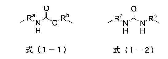
式(1-1)、および式(1-2)中、RaおよびRbは、それぞれ独立して、二価の有機基を表す。二価の有機基の定義は上記と同様であり、好ましくは、置換若しくは無置換の、メチレン基、エチレン基、プロピレン基、若しくはブチレン基などのアルキレン基、または、エチレンオキシド基、ジエチレンオキシド基、トリエチレンオキシド基、テトラエチレンオキシド基、ジプロピレンオキシド基、トリプロピレンオキシド基、テトラプロピレンオキシド基などのポリオキシアルキレン基などが挙げられる。
式(1)で表されるユニットの好適態様として、式(1-A)で表されるユニットが挙げられる。
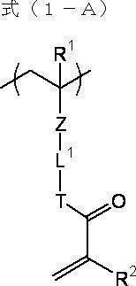
式(1-A)中、R1、R2、ZおよびL1は、式(1)で表されるユニット中の各基の定義と同じである。Tは、酸素原子、またはNR(Rは、水素原子またはアルキル基を表し、好ましくは、水素原子または炭素数1~5の無置換のアルキル基である。)を表す。
式(1-A)で表されるユニットの好適態様として、式(1-B)で表されるユニットが挙げられる。
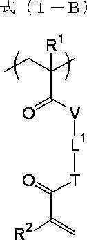
式(1-B)中、R1、R2、およびL1は、式(1-A)で表されるユニット中の各基の定義と同じである。VおよびTは、酸素原子、またはNR(Rは、水素原子またはアルキル基を表し、好ましくは、水素原子または炭素数1~5の無置換のアルキル基である。)を表す。
上記式(1-B)において、Tは、酸素原子であることが好ましい。
また、上記式(1-A)および式(1-B)において、L1は、無置換のアルキレン基、または、ウレタン結合若しくはウレア結合を有する二価の有機基が好ましく、ウレタン結合を有する二価の有機基がより好ましく、総炭素数1~9であるものが特に好ましい。
また、上記式(1-A)および式(1-B)において、L1は、無置換のアルキレン基、または、ウレタン結合若しくはウレア結合を有する二価の有機基が好ましく、ウレタン結合を有する二価の有機基がより好ましく、総炭素数1~9であるものが特に好ましい。
ポリマー中における式(1)で表されるユニットの含有量は特に制限されないが、反応性(重合性、硬化性)および絶縁層との密着性の点で、全ユニット(100モル%)に対して、5~50モル%が好ましく、5~40モル%がより好ましい。5モル%未満の場合、反応性(硬化性、重合性)が低下する場合があり、50モル%を超える場合、ポリマーの合成の際にゲル化が起きやすく、反応の制御が難しくなる。
ポリマーの好適態様として、以下の式(2)で表されるユニット(相互作用性基含有ユニット)を有するポリマーが挙げられる。該ユニットがポリマー中に含まれることにより、後述するめっき触媒またはその前駆体への吸着性が向上し、樹脂層20と後述する金属膜28との優れた密着性が担保される。

式(2)中、R5は、水素原子、又は、置換若しくは無置換のアルキル基を表す。R5で表される置換または無置換のアルキル基は、上述したR1~R4で表される置換または無置換のアルキル基と同義である。
R5としては、水素原子、メチル基、または、ヒドロキシ基若しくは臭素原子で置換されたメチル基が好ましい。
R5としては、水素原子、メチル基、または、ヒドロキシ基若しくは臭素原子で置換されたメチル基が好ましい。
XおよびL2は、それぞれ独立して、単結合、または置換若しく無置換の二価の有機基を表す。二価の有機基の定義は、上記ZおよびYで表される二価の有機基と同義であり、例えば、置換若しくは無置換の脂肪族炭化水素基、置換若しくは無置換の芳香族炭化水素基、-O-、-S-、-N(R)-(R:アルキル基)、-CO-、-NH-、-COO-、-CONH-、またはこれらを組み合わせた基などが挙げられる。
Xとしては、単結合、エステル基(-COO-)、アミド基(-CONH-)、エーテル基(-O-)、または置換若しくは無置換の芳香族炭化水素基などが好ましく挙げられ、より好ましくは単結合、エステル基(-COO-)、アミド基(-CONH-)である。
L2は、直鎖、分岐、若しくは環状のアルキレン基、芳香族基、またはこれらを組み合わせた基であることが好ましい。該アルキレン基と芳香族基とを組み合わせた基は、更に、エーテル基、エステル基、アミド基、ウレタン基、ウレア基を介していてもよい。
中でも、L2は総炭素数が1~15であることが好ましく、特に無置換であることが好ましい。なお、ここで、L2の総炭素数とは、L2で表される置換または無置換の二価の有機基に含まれる総炭素原子数を意味する。
具体的には、メチレン基、エチレン基、プロピレン基、ブチレン基、フェニレン基、およびこれらの基が、メトキシ基、ヒドロキシ基、塩素原子、臭素原子、フッ素原子等で置換されたもの、更には、これらを組み合わせた基が挙げられる。
中でも、L2は総炭素数が1~15であることが好ましく、特に無置換であることが好ましい。なお、ここで、L2の総炭素数とは、L2で表される置換または無置換の二価の有機基に含まれる総炭素原子数を意味する。
具体的には、メチレン基、エチレン基、プロピレン基、ブチレン基、フェニレン基、およびこれらの基が、メトキシ基、ヒドロキシ基、塩素原子、臭素原子、フッ素原子等で置換されたもの、更には、これらを組み合わせた基が挙げられる。
Wは、めっき触媒またはその前駆体と相互作用を形成する官能基(相互作用性基)を表し、その定義は上述の通りである。なかでも、めっき触媒またはその前駆体への吸着性に優れる点で、シアノ基またはカルボン酸基が好ましい。
なお、該ポリマー中においては、Wの種類が異なる2種以上の式(2)で表されるユニットを含んでいてもよく、得られる多層配線基板の接続信頼性や歩留りがより優れる点で、Wがシアノ基である式(2)で表されるユニットと、Wがカルボン酸基である式(2)で表されるユニットとが含まれることが好ましい。
式(2)で表されるユニットの好適態様として、式(2-A)で表されるユニットが挙げられる。

上記式(2-A)中、R5、L2およびWは、式(2)で表されるユニット中の各基の定義と同じである。Uは、酸素原子、またはNR’(R’は、水素原子、またはアルキル基を表し、好ましくは、水素原子、または炭素数1~5の無置換のアルキル基である。)を表す。
式(2-A)におけるL2は、直鎖、分岐、若しくは環状のアルキレン基、芳香族基(なかでも、二価の芳香族炭化水素基が好ましい)、またはこれらを組み合わせた基であることが好ましい。
特に、式(2-A)においては、L2中のWとの連結部位が、直鎖、分岐、または環状のアルキレン基を有する二価の有機基であることが好ましく、中でも、この二価の有機基が総炭素数1~10であることが好ましい。
また、別の好ましい態様としては、式(2-A)におけるL2中のWとの連結部位が、芳香族基を有する二価の有機基であることが好ましく、中でも、該二価の有機基が、総炭素数6~15であることが好ましい。
特に、式(2-A)においては、L2中のWとの連結部位が、直鎖、分岐、または環状のアルキレン基を有する二価の有機基であることが好ましく、中でも、この二価の有機基が総炭素数1~10であることが好ましい。
また、別の好ましい態様としては、式(2-A)におけるL2中のWとの連結部位が、芳香族基を有する二価の有機基であることが好ましく、中でも、該二価の有機基が、総炭素数6~15であることが好ましい。
ポリマー中における式(2)で表されるユニットの含有量は特に制限されないが、めっき触媒などに対する吸着性の点で、全ユニット(100モル%)に対して、5~94モル%が好ましく、10~80モル%がより好ましい。
ポリマー中における各ユニットの結合様式は特に限定されず、各ユニットがランダムに結合したランダム重合体であっても、各ユニットが同じ種類同士連結してブロック部を形成するブロックポリマーであってもよい。
ポリマーは、上述した式(1)で表されるユニット、式(2)で表されるユニット以外に、本発明の効果を損なわない範囲で、他のユニットを含んでいてもよい。
(樹脂層形成用組成物)
樹脂層形成用組成物には上記ポリマーが含有される。
樹脂層形成用組成物中のポリマーの含有量は特に制限されないが、組成物全量に対して、2~50質量%が好ましく、5~30質量%がより好ましい。上記範囲内であれば、組成物の取扱い性に優れ、樹脂層20の層厚の制御がしやすい。
樹脂層形成用組成物には上記ポリマーが含有される。
樹脂層形成用組成物中のポリマーの含有量は特に制限されないが、組成物全量に対して、2~50質量%が好ましく、5~30質量%がより好ましい。上記範囲内であれば、組成物の取扱い性に優れ、樹脂層20の層厚の制御がしやすい。
樹脂層形成用組成物は、上記ポリマー以外に、必要に応じて溶剤が含まれていてもよい。
使用できる溶剤としては、例えば、メタノール、エタノール、プロパノール、エチレングリコール、グリセリン、プロピレングリコールモノメチルエーテルなどのアルコール系溶剤、酢酸などの酸、アセトン、メチルエチルケトン、シクロヘキサノンなどのケトン系溶剤、ホルムアミド、ジメチルアセトアミド、N-メチルピロリドンなどのアミド系溶剤、アセトニトリル、プロピオニトリルなどのニトリル系溶剤、酢酸メチル、酢酸エチルなどのエステル系溶剤、ジメチルカーボネート、ジエチルカーボネートなどのカーボネート系溶剤、この他にも、エーテル系溶剤、グリコール系溶剤、アミン系溶剤、チオール系溶剤、ハロゲン系溶剤などが挙げられる。
この中でも、アミド系溶剤、ケトン系溶剤、ニトリル系溶剤、カーボネート系溶剤が好ましく、具体的には、アセトン、ジメチルアセトアミド、メチルエチルケトン、シクロヘキサノン、アセトニトリル、プロピオニトリル、N-メチルピロリドン、ジメチルカーボネートが好ましい。
使用できる溶剤としては、例えば、メタノール、エタノール、プロパノール、エチレングリコール、グリセリン、プロピレングリコールモノメチルエーテルなどのアルコール系溶剤、酢酸などの酸、アセトン、メチルエチルケトン、シクロヘキサノンなどのケトン系溶剤、ホルムアミド、ジメチルアセトアミド、N-メチルピロリドンなどのアミド系溶剤、アセトニトリル、プロピオニトリルなどのニトリル系溶剤、酢酸メチル、酢酸エチルなどのエステル系溶剤、ジメチルカーボネート、ジエチルカーボネートなどのカーボネート系溶剤、この他にも、エーテル系溶剤、グリコール系溶剤、アミン系溶剤、チオール系溶剤、ハロゲン系溶剤などが挙げられる。
この中でも、アミド系溶剤、ケトン系溶剤、ニトリル系溶剤、カーボネート系溶剤が好ましく、具体的には、アセトン、ジメチルアセトアミド、メチルエチルケトン、シクロヘキサノン、アセトニトリル、プロピオニトリル、N-メチルピロリドン、ジメチルカーボネートが好ましい。
樹脂層形成用組成物中の溶剤の含有量は特に制限されないが、組成物全量に対して、50~98質量%が好ましく、70~95質量%がより好ましい。上記範囲内であれば、組成物の取扱い性に優れ、樹脂層20の層厚の制御などがしやすい。
なお、樹脂層形成用組成物には、更に、界面活性剤、可塑剤、重合禁止剤、硬化剤、ラジカル発生剤、増感剤、ゴム成分(例えば、CTBN)、難燃化剤(例えば、りん系難燃化剤)、希釈剤やチキソトロピー化剤、顔料、消泡剤、レベリング剤、カップリング剤などを添加してもよい。
上述した樹脂層20および絶縁層16の材料は適宜選択されるが、低粗度かつ金属との強密着の点から、樹脂層20を構成するポリマーがアクリル系ポリマーまたはメタクリル系ポリマーであり、絶縁層16を構成する材料がエポキシ組成物またはポリイミドである組み合わせが好ましい。
特に好ましくは、樹脂層20を構成するポリマーがアクリル系ポリマーであり、絶縁層16を構成する材料がエポキシ組成物である組み合わせがより好ましい。
特に好ましくは、樹脂層20を構成するポリマーがアクリル系ポリマーであり、絶縁層16を構成する材料がエポキシ組成物である組み合わせがより好ましい。
<工程(E):仮支持体剥離工程>
工程(E)では、工程(D)で得られた積層体から仮支持体を剥離する。
より具体的には、図1(D)に示されるように、本工程においては、工程(D)において絶縁層16上に堆積された樹脂層形成用積層フィルム24を備える積層体26から、仮支持体22を剥離する。仮支持体22を剥離することにより、絶縁層16と密着した樹脂層20が積層体中に残存し、ビアホール18上に配置されていた樹脂層20は仮支持体22と共に積層体26から除去される。言い換えると、本工程で、絶縁層16上に樹脂層20を形成することができる。
工程(E)では、工程(D)で得られた積層体から仮支持体を剥離する。
より具体的には、図1(D)に示されるように、本工程においては、工程(D)において絶縁層16上に堆積された樹脂層形成用積層フィルム24を備える積層体26から、仮支持体22を剥離する。仮支持体22を剥離することにより、絶縁層16と密着した樹脂層20が積層体中に残存し、ビアホール18上に配置されていた樹脂層20は仮支持体22と共に積層体26から除去される。言い換えると、本工程で、絶縁層16上に樹脂層20を形成することができる。
仮支持体22の剥離条件は、使用される材料に応じて、適宜最適な条件が選択される。なかでも、ビアホール18と重なる余分な樹脂層20を積層体26から除去しやすい点から、工程(E)における樹脂層20の温度は、0~40℃が好ましく、10~40℃がより好ましく、15~35℃がさらに好ましい。
(好適態様)
工程(E)において、ビアホール18と重なる余分な樹脂層20を除去しやすい点から、樹脂層20と絶縁層16の単位面積当たりの界面剥離強度σ(A1)と、樹脂層20と仮支持体22の単位面積当たりの界面剥離強度σ(B1)と、樹脂層20の破断応力σ(C1)が、以下式(X)の関係を満足することが好ましい。
式(X) σ(A1)>σ(B1)>σ(C1)
工程(E)において、ビアホール18と重なる余分な樹脂層20を除去しやすい点から、樹脂層20と絶縁層16の単位面積当たりの界面剥離強度σ(A1)と、樹脂層20と仮支持体22の単位面積当たりの界面剥離強度σ(B1)と、樹脂層20の破断応力σ(C1)が、以下式(X)の関係を満足することが好ましい。
式(X) σ(A1)>σ(B1)>σ(C1)
上記式(X)においては、ビアホール18と重なる余分な樹脂層20を基板上から除去するには、まずビアホール18と重なる余分な樹脂層20が切り取られること、すなわち樹脂層20が破断して仮支持体22と接着した状態で共に除去されることが好ましく、そのためにはσ(C1)が最も低いことが好ましい。
続いて仮支持体22が剥れるためには、仮支持体22と樹脂層20の界面剥離強度σ(B1)が樹脂層20と絶縁層16の界面剥離強度σ(A1)よりも低いことが好ましい。仮に、σ(B1)がσ(A1)よりも強すぎると、所定の領域にラミネートされた樹脂層20が絶縁層16上から剥離される場合もあり、転写不良となることもある。したがって、上記式(X)が、ビアホール18と重なる余分な樹脂層20を積層体26から除去する条件となることを意味する。
続いて仮支持体22が剥れるためには、仮支持体22と樹脂層20の界面剥離強度σ(B1)が樹脂層20と絶縁層16の界面剥離強度σ(A1)よりも低いことが好ましい。仮に、σ(B1)がσ(A1)よりも強すぎると、所定の領域にラミネートされた樹脂層20が絶縁層16上から剥離される場合もあり、転写不良となることもある。したがって、上記式(X)が、ビアホール18と重なる余分な樹脂層20を積層体26から除去する条件となることを意味する。
樹脂層20と絶縁層16との単位面積当たりの界面剥離強度σ(A1)は、50~500MPaであることが好ましく、100~400MPaであることがより好ましい。
樹脂層20と仮支持体22との単位面積当たりの界面剥離強度σ(B1)は、10~300MPaであることが好ましく、50~200MPaであることがより好ましい。
樹脂層20の破断応力σ(C1)は、0.01~150MPaであることが好ましく、0.05~100MPaであることがより好ましい。
樹脂層20と仮支持体22との単位面積当たりの界面剥離強度σ(B1)は、10~300MPaであることが好ましく、50~200MPaであることがより好ましい。
樹脂層20の破断応力σ(C1)は、0.01~150MPaであることが好ましく、0.05~100MPaであることがより好ましい。
余分な樹脂層20が積層体に残存しにくい点から、界面剥離強度σ(A1)と界面剥離強度σ(B1)との差は、5~70MPaであることが好ましい。
余分な樹脂層20が積層体に残存しにくい点から、界面剥離強度σ(B1)と破断応力σ(C1)との差は、20~70MPaであることが好ましい。
余分な樹脂層20が積層体に残存しにくい点から、界面剥離強度σ(B1)と破断応力σ(C1)との差は、20~70MPaであることが好ましい。
<工程(F):めっき工程>
工程(F)では、上記(E)工程後にビアホールの壁面および樹脂層に対してめっき触媒またはその前駆体を付与した後、めっきを行う。
より具体的には、図1(E)に示されるように、めっきを行うことにより、金属配線14と接触し、導通する金属膜28を形成することができる。
工程(F)では、上記(E)工程後にビアホールの壁面および樹脂層に対してめっき触媒またはその前駆体を付与した後、めっきを行う。
より具体的には、図1(E)に示されるように、めっきを行うことにより、金属配線14と接触し、導通する金属膜28を形成することができる。
本工程においては、主に樹脂層20中に含まれる相互作用性基が、その機能に応じて、付与されためっき触媒またはその前駆体を付着(吸着)する。
めっき触媒またはその前駆体としては、後述するめっき処理における、めっきの触媒や電極として機能するものが挙げられる。そのため、めっき触媒またはその前駆体の種類は、めっきの種類により適宜決定される。
なお、本工程において用いられるめっき触媒またはその前駆体は、無電解めっき触媒またはその前駆体であることが好ましい。なかでも、めっき触媒またはその前駆体は、還元電位の点から、Pd、Ag、またはCuを含む化合物であることが好ましい。
以下、まず、無電解めっきまたはその前駆体について詳述する。
めっき触媒またはその前駆体としては、後述するめっき処理における、めっきの触媒や電極として機能するものが挙げられる。そのため、めっき触媒またはその前駆体の種類は、めっきの種類により適宜決定される。
なお、本工程において用いられるめっき触媒またはその前駆体は、無電解めっき触媒またはその前駆体であることが好ましい。なかでも、めっき触媒またはその前駆体は、還元電位の点から、Pd、Ag、またはCuを含む化合物であることが好ましい。
以下、まず、無電解めっきまたはその前駆体について詳述する。
(無電解めっき触媒)
無電解めっき触媒は、無電解めっき時の活性核となるものであれば、如何なるものも用いることができ、具体的には、自己触媒還元反応の触媒能を有する金属(例えば、Niよりイオン化傾向の低い無電解めっきできる金属として知られるもの)などが挙げられ、具体的には、Pd、Ag、Cu、Ni、Al、Fe、Coなどが挙げられる。中でも、多座配位可能なものが好ましく、配位可能な官能基の種類数、触媒能の高さから、Ag、Pd、Cuが特に好ましい。
この無電解めっき触媒として、金属コロイドを用いてもよい。一般に、金属コロイドは、荷電を持った界面活性剤又は荷電を持った保護剤が存在する溶液中において、金属イオンを還元することにより作製することができる。金属コロイドの荷電は、ここで使用される界面活性剤又は保護剤により調節することができる。
無電解めっき触媒は、無電解めっき時の活性核となるものであれば、如何なるものも用いることができ、具体的には、自己触媒還元反応の触媒能を有する金属(例えば、Niよりイオン化傾向の低い無電解めっきできる金属として知られるもの)などが挙げられ、具体的には、Pd、Ag、Cu、Ni、Al、Fe、Coなどが挙げられる。中でも、多座配位可能なものが好ましく、配位可能な官能基の種類数、触媒能の高さから、Ag、Pd、Cuが特に好ましい。
この無電解めっき触媒として、金属コロイドを用いてもよい。一般に、金属コロイドは、荷電を持った界面活性剤又は荷電を持った保護剤が存在する溶液中において、金属イオンを還元することにより作製することができる。金属コロイドの荷電は、ここで使用される界面活性剤又は保護剤により調節することができる。
(無電解めっき触媒前駆体)
無電解めっき触媒前駆体とは、化学反応により無電解めっき触媒となりうるものであれば、特に制限なく使用することができる。主には、上記無電解めっき触媒として挙げた金属の金属イオンが用いられる。無電解めっき触媒前駆体である金属イオンは、還元反応により無電解めっき触媒である0価金属になる。無電解めっき触媒前駆体である金属イオンは、ビアホール18の壁面および樹脂層20へ付与した後、無電解めっき浴への浸漬前に、別途還元反応により0価金属に変化させて無電解めっき触媒としてもよいし、無電解めっき触媒前駆体のまま無電解めっき浴に浸漬し、無電解めっき浴中の還元剤により金属(無電解めっき触媒)に変化させてもよい。
無電解めっき触媒前駆体とは、化学反応により無電解めっき触媒となりうるものであれば、特に制限なく使用することができる。主には、上記無電解めっき触媒として挙げた金属の金属イオンが用いられる。無電解めっき触媒前駆体である金属イオンは、還元反応により無電解めっき触媒である0価金属になる。無電解めっき触媒前駆体である金属イオンは、ビアホール18の壁面および樹脂層20へ付与した後、無電解めっき浴への浸漬前に、別途還元反応により0価金属に変化させて無電解めっき触媒としてもよいし、無電解めっき触媒前駆体のまま無電解めっき浴に浸漬し、無電解めっき浴中の還元剤により金属(無電解めっき触媒)に変化させてもよい。
無電解めっき触媒前駆体である金属イオンは、金属塩を用いてビアホール18の壁面および樹脂層20(樹脂層20内部およびその表面)に付与することが好ましい。使用される金属塩としては、適切な溶媒に溶解して金属イオンと塩基(陰イオン)とに解離されるものであれば特に制限はなく、M(NO3)n、MCln、M2/n(SO4)、M3/n(PO4)Pd(OAc)n(Mは、n価の金属原子を表す)などが挙げられる。金属イオンとしては、上記の金属塩が解離したものを好適に用いることができる。具体例としては、例えば、Agイオン、Cuイオン、Alイオン、Niイオン、Coイオン、Feイオン、Pdイオンが挙げられ、中でも、多座配位可能なものが好ましく、特に、配位可能な官能基の種類数、及び触媒能の点で、Agイオン、Pdイオンが好ましい。
本発明で用いられる無電解めっき触媒またはその前駆体の好ましい例の一つとして、パラジウム化合物が挙げられる。このパラジウム化合物は、めっき処理時に活性核となり金属を析出させる役割を果たす、めっき触媒(パラジウム)またはその前駆体(パラジウムイオン)として作用する。パラジウム化合物としては、パラジウムを含み、めっき処理の際に核として作用すれば、特に限定されないが、例えば、パラジウム(II)塩、パラジウム(0)錯体、パラジウムコロイドなどが挙げられる。
パラジウム塩としては、例えば、酢酸パラジウム、塩化パラジウム、硝酸パラジウム、臭化パラジウム、炭酸パラジウム、硫酸パラジウム、ビス(ベンゾニトリル)ジクロロパラジウム(II)、ビス(アセトニトリル)ジクロロパラジウム(II)、ビス(エチレンジアミン)パラジウム(II)塩化物などが挙げられる。なかでも、取り扱いやすさと溶解性の点で、硝酸パラジウム、酢酸パラジウム、硫酸パラジウム、ビス(アセトニトリル)ジクロロパラジウム(II)が好ましい。
パラジウム錯体としては、テトラキストリフェニルホスフィンパラジウム錯体、ジパラジウムトリスベンジリデンアセトン錯体などが挙げられる。
パラジウムコロイドは、パラジウム(0)から構成される粒子で、その大きさは特に制限されないが、液中での安定性の観点から、5nm~300nmが好ましく、10nm~100nmがより好ましい。パラジウムコロイドは、必要に応じて、他の金属を含んでいてもよく、他の金属としては、例えば、スズなどが挙げられる。パラジウムコロイドとしては、例えば、スズ-パラジウムコロイドなどが挙げられる。なお、パラジウムコロイドは、公知の方法で合成してもよいし、市販品を使用してもよい。例えば、荷電を持った界面活性剤又は荷電を持った保護剤が存在する溶液中において、パラジウムイオンを還元することによりパラジウムコロイドを作製することができる。
パラジウム錯体としては、テトラキストリフェニルホスフィンパラジウム錯体、ジパラジウムトリスベンジリデンアセトン錯体などが挙げられる。
パラジウムコロイドは、パラジウム(0)から構成される粒子で、その大きさは特に制限されないが、液中での安定性の観点から、5nm~300nmが好ましく、10nm~100nmがより好ましい。パラジウムコロイドは、必要に応じて、他の金属を含んでいてもよく、他の金属としては、例えば、スズなどが挙げられる。パラジウムコロイドとしては、例えば、スズ-パラジウムコロイドなどが挙げられる。なお、パラジウムコロイドは、公知の方法で合成してもよいし、市販品を使用してもよい。例えば、荷電を持った界面活性剤又は荷電を持った保護剤が存在する溶液中において、パラジウムイオンを還元することによりパラジウムコロイドを作製することができる。
(その他の触媒)
本工程において、無電解めっきを行わず直接電気めっきを行うために用いられる触媒として、上述した以外の0価金属を使用することもできる。
本工程において、無電解めっきを行わず直接電気めっきを行うために用いられる触媒として、上述した以外の0価金属を使用することもできる。
無電解めっき触媒である金属、または、無電解めっき触媒前駆体である金属塩をビアホール18の壁面および樹脂層20に付与する方法としては、金属を適当な分散媒に分散した分散液、又は、金属塩を適切な溶媒で溶解し、解離した金属イオンを含む溶液(めっき触媒液)を調製し、その分散液又は溶液をビアホール18の壁面および樹脂層20上に塗布するか、或いは、その分散液又は溶液中に樹脂層20が形成された積層体を浸漬すればよい。
また、工程(E)において、樹脂層形成用組成物中に無電解めっき触媒またはその前駆体を添加する方法を用いてもよい。
重合性基及び相互作用性基を有するポリマーと、無電解めっき触媒またはその前駆体とを含有する組成物を、仮支持体22上に塗布することにより、相互作用性基を有し、且つ、めっき触媒またはその前駆体とを含有する樹脂層20を形成することができる。
また、工程(E)において、樹脂層形成用組成物中に無電解めっき触媒またはその前駆体を添加する方法を用いてもよい。
重合性基及び相互作用性基を有するポリマーと、無電解めっき触媒またはその前駆体とを含有する組成物を、仮支持体22上に塗布することにより、相互作用性基を有し、且つ、めっき触媒またはその前駆体とを含有する樹脂層20を形成することができる。
(有機溶剤、及び水)
上記のようなめっき触媒又はその前駆体は、分散液または溶液(めっき触媒液)としてビアホール18の壁面および樹脂層20に付与されることができる。なお、めっき触媒液には、有機溶剤や水が用いられる。
有機溶剤を含有することで、ビアホール18の壁面および樹脂層20に対するめっき触媒またはその前駆体の浸透性が向上し、相互作用性基に効率よくめっき触媒またはその前駆体を吸着させることができる。
上記のようなめっき触媒又はその前駆体は、分散液または溶液(めっき触媒液)としてビアホール18の壁面および樹脂層20に付与されることができる。なお、めっき触媒液には、有機溶剤や水が用いられる。
有機溶剤を含有することで、ビアホール18の壁面および樹脂層20に対するめっき触媒またはその前駆体の浸透性が向上し、相互作用性基に効率よくめっき触媒またはその前駆体を吸着させることができる。
触媒液には、水を用いてもよく、この水としては、不純物を含まないことが好ましく、そのような観点からは、RO水や脱イオン水、蒸留水、精製水などを用いるのが好ましく、脱イオン水や蒸留水を用いるのが特に好ましい。
触媒液の調製に用いられる有機溶剤としては、ビアホール18の壁面および樹脂層20に浸透しうる溶剤であれば特に制限は無いが、具体的には、アセトン、アセト酢酸メチル、アセト酢酸エチル、エチレングリコールジアセテート、シクロヘキサノン、アセチルアセトン、アセトフェノン、2-(1-シクロヘキセニル)、プロピレングリコールジアセテート、トリアセチン、ジエチレングリコールジアセテート、ジオキサン、N-メチルピロリドン、ジメチルカーボネート、ジメチルセロソルブなどを用いることができる。
特に、めっき触媒またはその前駆体との相溶性、並びに、ビアホール18の壁面および樹脂層20への浸透性の観点では水溶性の有機溶剤が好ましく、アセトン、ジメチルカーボネート、ジメチルセロソルブ、トリエチレングリコールモノメチルエーテル、ジエチレングリコールジメチルエーテル、ジエチレングリコールジエチルエーテルが好ましい。
溶剤の含有量は、めっき触媒液全量に対して0.5~40質量%が好ましく、5~30質量%であることがより好ましく、5~20質量%の範囲であることが特に好ましい。
めっき触媒液には、めっき触媒またはその前駆体及び主たる溶剤である水に加え、本発明の効果を損なわない範囲において、目的に応じて他の添加剤を含有することができる。他の添加剤としては、以下に示すものが挙げられる。
例えば、膨潤剤(ケトン、アルデヒド、エーテル、エステル類等の有機化合物など)や、界面活性剤(アニオン性、カチオン性、双性、ノニオン性および低分子性または高分子性など)などが挙げられる。
めっき触媒液には、めっき触媒またはその前駆体及び主たる溶剤である水に加え、本発明の効果を損なわない範囲において、目的に応じて他の添加剤を含有することができる。他の添加剤としては、以下に示すものが挙げられる。
例えば、膨潤剤(ケトン、アルデヒド、エーテル、エステル類等の有機化合物など)や、界面活性剤(アニオン性、カチオン性、双性、ノニオン性および低分子性または高分子性など)などが挙げられる。
上記のようにめっき触媒またはその前駆体を接触させることで、特に、樹脂層20中の相互作用性基に、ファンデルワールス力のような分子間力による相互作用、又は、孤立電子対による配位結合による相互作用を利用して、めっき触媒またはその前駆体を吸着させることができる。
このような吸着を充分に行わせるという観点からは、分散液、溶液、組成物中の金属濃度、又は溶液中の金属イオン濃度は、0.001~50質量%の範囲であることが好ましく、0.005~30質量%の範囲であることが更に好ましい。また、接触時間としては、30秒~24時間程度であることが好ましく、1分~1時間程度であることがより好ましい。
この工程(F)の前段では、ビアホール18の壁面および樹脂層20にめっき触媒またはその前駆体を付与することができ、特に、樹脂層20中の相互作用性基とめっき触媒またはその前駆体との間に相互作用を形成することができる。
このような吸着を充分に行わせるという観点からは、分散液、溶液、組成物中の金属濃度、又は溶液中の金属イオン濃度は、0.001~50質量%の範囲であることが好ましく、0.005~30質量%の範囲であることが更に好ましい。また、接触時間としては、30秒~24時間程度であることが好ましく、1分~1時間程度であることがより好ましい。
この工程(F)の前段では、ビアホール18の壁面および樹脂層20にめっき触媒またはその前駆体を付与することができ、特に、樹脂層20中の相互作用性基とめっき触媒またはその前駆体との間に相互作用を形成することができる。
(めっき処理)
その後、無電解めっき触媒またはその前駆体が付与されたビアホール18の壁面および樹脂層20に対し、めっきを行うことで、樹脂層20の表面に金属層(めっき膜)28が形成される〔図1(E)〕。形成された金属層28は、第2の金属配線として機能し、優れた導電性、密着性を有する。
金属層28の厚みは特に制限されないが、セミアディティブ法およびサブトラクティブ法にて配線形成する点で、0.2~30μmが好ましく、0.4~20μmがより好ましい。なお、厚みは、樹脂層20の表面から金属層28の表面までの厚みを意味する。
その後、無電解めっき触媒またはその前駆体が付与されたビアホール18の壁面および樹脂層20に対し、めっきを行うことで、樹脂層20の表面に金属層(めっき膜)28が形成される〔図1(E)〕。形成された金属層28は、第2の金属配線として機能し、優れた導電性、密着性を有する。
金属層28の厚みは特に制限されないが、セミアディティブ法およびサブトラクティブ法にて配線形成する点で、0.2~30μmが好ましく、0.4~20μmがより好ましい。なお、厚みは、樹脂層20の表面から金属層28の表面までの厚みを意味する。
本工程で行われるめっきの種類は、無電解めっき、電気めっきが挙げられ、めっき触媒またはその前駆体の機能によって、適宜選択することができる。なかでも、樹脂層20中に発現するハイブリッド構造の形成性及び密着性向上の点から、無電解めっきを行うことが好ましい。また、所望の膜厚のめっき層を得るために、無電解めっきの後に、更に電気めっきを行うことがより好ましい態様である。
以下、本工程において好適に行われるめっきについて説明する。
以下、本工程において好適に行われるめっきについて説明する。
(無電解めっき)
無電解めっきとは、めっきとして析出させたい金属イオンを溶かした溶液を用いて、化学反応によって金属を析出させる操作のことをいう。
本工程における無電解めっきは、例えば、無電解めっき触媒が付与された積層体を、水洗して余分な無電解めっき触媒(金属)を除去した後、無電解めっき浴に浸漬して行う。使用される無電解めっき浴としては一般的に知られている無電解めっき浴を使用することができる。
無電解めっきとは、めっきとして析出させたい金属イオンを溶かした溶液を用いて、化学反応によって金属を析出させる操作のことをいう。
本工程における無電解めっきは、例えば、無電解めっき触媒が付与された積層体を、水洗して余分な無電解めっき触媒(金属)を除去した後、無電解めっき浴に浸漬して行う。使用される無電解めっき浴としては一般的に知られている無電解めっき浴を使用することができる。
また、無電解めっき触媒前駆体が付与された積層体を、無電解めっき触媒前駆体がビアホール18の壁面および樹脂層20に吸着又は含浸した状態で無電解めっき浴に浸漬する場合には、積層体を水洗して余分な前駆体(金属塩など)を除去した後、無電解めっき浴中へ浸漬される。この場合には、無電解めっき浴中において、めっき触媒前駆体の還元とこれに引き続き無電解めっきが行われる。ここで使用される無電解めっき浴としても、上記同様、一般的に知られている無電解めっき浴を使用することができる。
なお、無電解めっき触媒前駆体の還元は、上記のような無電解めっき液を用いる態様とは別に、触媒活性化液(還元液)を準備し、無電解めっき前の別工程として行うことも可能である。触媒活性化液は、無電解めっき触媒前駆体(主に金属イオン)を0価金属に還元できる還元剤を溶解した液で、その濃度は0.1~50質量%が好ましく、1~30質量%がより好ましい。還元剤としては、水素化ホウ素ナトリウム、ジメチルアミンボランのようなホウ素系還元剤、ホルムアルデヒド、次亜リン酸などの還元剤を使用することが可能である。
なお、無電解めっき触媒前駆体の還元は、上記のような無電解めっき液を用いる態様とは別に、触媒活性化液(還元液)を準備し、無電解めっき前の別工程として行うことも可能である。触媒活性化液は、無電解めっき触媒前駆体(主に金属イオン)を0価金属に還元できる還元剤を溶解した液で、その濃度は0.1~50質量%が好ましく、1~30質量%がより好ましい。還元剤としては、水素化ホウ素ナトリウム、ジメチルアミンボランのようなホウ素系還元剤、ホルムアルデヒド、次亜リン酸などの還元剤を使用することが可能である。
一般的な無電解めっき浴の組成としては、溶剤の他に、1.めっき用の金属イオン、2.還元剤、3.金属イオンの安定性を向上させる添加剤(安定剤)が主に含まれている。このめっき浴には、これらに加えて、めっき浴の安定剤など公知の添加物が含まれていてもよい。
無電解めっき浴に用いられる溶剤としては水、または有機溶剤が挙げられる。有機溶剤としては、水に可能な溶剤である必要があり、その点から、アセトンなどのケトン類、メタノール、エタノール、イソプロパノールなどのアルコール類が好ましく用いられる。
無電解めっき浴に用いられる金属の種類としては、銅、すず、鉛、ニッケル、金、パラジウム、ロジウムが知られており、中でも、導電性の観点からは、銅、金が特に好ましい。また、上記金属に合わせて最適な還元剤、添加物が適宜選択される。
めっき浴への浸漬時間としては、1分~6時間程度であることが好ましく、1分~3時間程度であることがより好ましい。
(電気めっき)
本工程おいては、付与されためっき触媒またはその前駆体が電極としての機能を有する場合、その触媒またはその前駆体が付与されたビアホール18の壁面および樹脂層20に対して、電気めっきを行うことができる。また、前述の無電解めっきの後、形成されためっき膜を電極とし、更に、電気めっきを行ってもよい。これにより基板との密着性に優れた無電解めっき膜をベースとして、そこに新たに任意の厚みをもつ金属層28を容易に形成することができる。このように、無電解めっきの後に、電気めっきを行うことで、金属層28を目的に応じた厚みに形成しうる。
本工程おいては、付与されためっき触媒またはその前駆体が電極としての機能を有する場合、その触媒またはその前駆体が付与されたビアホール18の壁面および樹脂層20に対して、電気めっきを行うことができる。また、前述の無電解めっきの後、形成されためっき膜を電極とし、更に、電気めっきを行ってもよい。これにより基板との密着性に優れた無電解めっき膜をベースとして、そこに新たに任意の厚みをもつ金属層28を容易に形成することができる。このように、無電解めっきの後に、電気めっきを行うことで、金属層28を目的に応じた厚みに形成しうる。
電気めっきの方法としては、従来公知の方法を用いることができる。なお、電気めっきに用いられる金属としては、例えば、銅、クロム、鉛、ニッケル、金、銀、すず、亜鉛などが挙げられ、導電性の観点から、銅、金、銀が好ましく、銅がより好ましい。
また、電気めっきにより得られる金属層の厚みについては、用途に応じて異なるものであり、めっき浴中に含まれる金属濃度、または、電流密度などを調整することでコントロールすることができる。
本発明において、めっき処理(無電解めっき、または電気めっき)により、樹脂層20中に析出した金属が、該層中でフラクタル状の微細構造体として形成されていることによって、金属層28と樹脂層20との密着性を更に向上させることができる。
樹脂層20中に存在する金属量は、基板断面を金属顕微鏡にて写真撮影したとき、樹脂層20の最表面から深さ0.5μmまでの領域に占める金属の割合が5~50面積%であり、樹脂層20と金属界面の算術平均粗さRa(JIS B0633-2001)が0.05μm~0.5μmである場合に、更に強い密着力が発現される。
樹脂層20中に存在する金属量は、基板断面を金属顕微鏡にて写真撮影したとき、樹脂層20の最表面から深さ0.5μmまでの領域に占める金属の割合が5~50面積%であり、樹脂層20と金属界面の算術平均粗さRa(JIS B0633-2001)が0.05μm~0.5μmである場合に、更に強い密着力が発現される。
以上、本発明においては、前述の(A)~(F)の工程を経ることで、ビアによる層間接続がなされ、且つ、微細配線を有する多層配線基板が製造される。
<任意工程(K):エネルギー付与工程>
上記工程(E)と工程(F)との間に、絶縁層16上に配置された樹脂層20に対して、エネルギー付与する工程を設けてもよい。該工程を設けることにより、重合性基を介して該ポリマー同士の反応が進行すると共に、樹脂層20中の該ポリマーが隣接する絶縁層16の表面と直接化学結合を生成し、絶縁層16と強固に結合した樹脂層20を形成することができる。
上記工程(E)と工程(F)との間に、絶縁層16上に配置された樹脂層20に対して、エネルギー付与する工程を設けてもよい。該工程を設けることにより、重合性基を介して該ポリマー同士の反応が進行すると共に、樹脂層20中の該ポリマーが隣接する絶縁層16の表面と直接化学結合を生成し、絶縁層16と強固に結合した樹脂層20を形成することができる。
(エネルギー付与方法)
エネルギー付与の方法としては、露光処理または加熱処理などが挙げられる。露光の場合、例えば、輻射線照射を用いることができる。例えば、UVランプ、可視光線などによる光照射が可能である。光源としては、例えば、水銀灯、メタルハライドランプ、キセノンランプ、ケミカルランプ、カーボンアーク灯、等がある。放射線としては、電子線、X線、イオンビーム、遠赤外線などがある。また、g線、i線、Deep-UV光、高密度エネルギービーム(レーザビーム)も使用される。
また、熱記録ヘッド等により加熱する方法、赤外線レーザによる走査露光などの方法が挙げられ、さらには、キセノン放電灯などの高照度フラッシュ露光や赤外線ランプ露光なども好適な方法として挙げられる。
エネルギー付与に要する時間としては、使用されるポリマーの構造及び光源により異なるが、通常、10秒~5時間の間である。
エネルギー付与の方法としては、露光処理または加熱処理などが挙げられる。露光の場合、例えば、輻射線照射を用いることができる。例えば、UVランプ、可視光線などによる光照射が可能である。光源としては、例えば、水銀灯、メタルハライドランプ、キセノンランプ、ケミカルランプ、カーボンアーク灯、等がある。放射線としては、電子線、X線、イオンビーム、遠赤外線などがある。また、g線、i線、Deep-UV光、高密度エネルギービーム(レーザビーム)も使用される。
また、熱記録ヘッド等により加熱する方法、赤外線レーザによる走査露光などの方法が挙げられ、さらには、キセノン放電灯などの高照度フラッシュ露光や赤外線ランプ露光なども好適な方法として挙げられる。
エネルギー付与に要する時間としては、使用されるポリマーの構造及び光源により異なるが、通常、10秒~5時間の間である。
なお、エネルギーの付与を露光にて行う場合、その露光パワーは、グラフト重合を容易に進行させるため、また、生成されたグラフトポリマーの分解を抑制するため、10~10000mJ/cm2の範囲であることが好ましく、より好ましくは50~7000mJ/cm2の範囲である。
<第2の実施態様>
本発明の多層配線基板の製造方法の他の実施態様(第2の実施態様とも称する)としては、上記工程(D)および(E)の代わりに、以下の工程(G)~工程(J)をこの順に実施する態様が挙げられる。
(G)工程(C)後に、仮支持体と、仮支持体上に密着補助層とを備える密着補助層形成用積層フィルムを、絶縁層上に、密着補助層とデスミア処理が施された絶縁層とが接するようにラミネートし、積層体を得る工程
(H)工程(G)後に、積層体から仮支持体を剥離する工程
(I)工程(H)後に、仮支持体と、仮支持体上にめっき触媒またはその前駆体と相互作用を形成する官能基、及び、重合性基を含有するポリマーを含む樹脂層とを備える樹脂層形成用積層フィルムを、密着補助層上に、樹脂層と密着補助層とが接するようにラミネートし、積層体を得る工程
(J)工程(I)後に、積層体から仮支持体を剥離する工程
上記第2の実施態様であれば、密着補助層により絶縁層と樹脂層との接着性がより向上すると共に、得られる多層配線基板の歩留まりがより向上する。
以下に、上記各工程の手順について説明する。
本発明の多層配線基板の製造方法の他の実施態様(第2の実施態様とも称する)としては、上記工程(D)および(E)の代わりに、以下の工程(G)~工程(J)をこの順に実施する態様が挙げられる。
(G)工程(C)後に、仮支持体と、仮支持体上に密着補助層とを備える密着補助層形成用積層フィルムを、絶縁層上に、密着補助層とデスミア処理が施された絶縁層とが接するようにラミネートし、積層体を得る工程
(H)工程(G)後に、積層体から仮支持体を剥離する工程
(I)工程(H)後に、仮支持体と、仮支持体上にめっき触媒またはその前駆体と相互作用を形成する官能基、及び、重合性基を含有するポリマーを含む樹脂層とを備える樹脂層形成用積層フィルムを、密着補助層上に、樹脂層と密着補助層とが接するようにラミネートし、積層体を得る工程
(J)工程(I)後に、積層体から仮支持体を剥離する工程
上記第2の実施態様であれば、密着補助層により絶縁層と樹脂層との接着性がより向上すると共に、得られる多層配線基板の歩留まりがより向上する。
以下に、上記各工程の手順について説明する。
<工程(G):積層体形成工程>
工程(G)は、上記工程(C)後に、仮支持体と、仮支持体上に密着補助層とを備える密着補助層形成用積層フィルムを、絶縁層上に、密着補助層とデスミア処理が施された絶縁層とが接するようにラミネートし、積層体を得る。
より具体的には、図2(A)に示されるように、本工程においては、絶縁層16上に、仮支持体22と仮支持体22上に設けられた密着補助層30とを備える密着補助層形成用積層フィルム32を、密着補助層30が絶縁層16と接するようにラミネートして、積層体34を得る。
工程(G)は、上記工程(C)後に、仮支持体と、仮支持体上に密着補助層とを備える密着補助層形成用積層フィルムを、絶縁層上に、密着補助層とデスミア処理が施された絶縁層とが接するようにラミネートし、積層体を得る。
より具体的には、図2(A)に示されるように、本工程においては、絶縁層16上に、仮支持体22と仮支持体22上に設けられた密着補助層30とを備える密着補助層形成用積層フィルム32を、密着補助層30が絶縁層16と接するようにラミネートして、積層体34を得る。
密着補助層形成用積層フィルム32を、密着補助層30が絶縁層16と接するように絶縁層16上にラミネートする方式は特に限定されず、バッチ式であってもロールでの連続式であってもよい。
密着補助層形成用積層フィルム32をラミネートする際の密着補助層30の温度Tは、上述した工程(D)の樹脂層20の条件と同じく、密着補助層のガラス転移温度以上で、ガラス転移温度+60℃以下である。好ましい態様は、上記樹脂層20と同じである。
また、密着補助層30のガラス転移温度の好ましい範囲は、上述した樹脂層20の範囲と同じである。
密着補助層30のヤング率は、上述した工程(D)の樹脂層20の条件と同じく、0.16×10⁶~100×106Paである。ヤング率の好ましい範囲は、上記樹脂層20と同じである。
さらに、密着補助層30の破断点伸度は、上述した工程(D)の樹脂層20の条件と同じく、100%以下である。破断点伸度の好ましい範囲は、上記樹脂層20と同じである。
密着補助層形成用積層フィルム32をラミネートする際の密着補助層30の温度Tは、上述した工程(D)の樹脂層20の条件と同じく、密着補助層のガラス転移温度以上で、ガラス転移温度+60℃以下である。好ましい態様は、上記樹脂層20と同じである。
また、密着補助層30のガラス転移温度の好ましい範囲は、上述した樹脂層20の範囲と同じである。
密着補助層30のヤング率は、上述した工程(D)の樹脂層20の条件と同じく、0.16×10⁶~100×106Paである。ヤング率の好ましい範囲は、上記樹脂層20と同じである。
さらに、密着補助層30の破断点伸度は、上述した工程(D)の樹脂層20の条件と同じく、100%以下である。破断点伸度の好ましい範囲は、上記樹脂層20と同じである。
ラミネート時に、密着補助層30と絶縁層16との密着を助けるために密着補助層形成用積層フィルム32に加えられる圧力(圧着圧力)Pの好ましい範囲は、上記樹脂層形成用積層フィルムに加えられる圧力の範囲と同じである。
また、工程(G)においても、上述した工程(D)と同じく、ラミネート時の密着補助層30の温度T、温度Tにおける密着補助層30のヤング率E(T)、密着補助層30の破断点伸度が上記範囲であり、密着補助層形成用積層フィルム32に加えられる圧力Pと、Log(E(T))とが、図3に示される、上記式(I)~(IV)で表される直線で囲まれた範囲に存在する。
(密着補助層形成用積層フィルム)
次に、本工程で使用される密着補助層形成用積層フィルム32を構成する仮支持体22と密着補助層30について詳述する。
仮支持体22は、上述した通りであり、その好適な態様も上記と同様である。
次に、本工程で使用される密着補助層形成用積層フィルム32を構成する仮支持体22と密着補助層30について詳述する。
仮支持体22は、上述した通りであり、その好適な態様も上記と同様である。
(密着補助層30)
密着補助層30は、絶縁層16と樹脂層20との接着性を補助する役割を果たす。
密着補助層30は、樹脂層20との結合反応の開始点となる活性種を与え、それを起点として密着補助層30と樹脂層20との間に多くの結合を生成させることができる。例えば、表面グラフト重合法等を用いる場合に有用である。
より具体的には、密着補助層30としては、重合開始剤を含有する層(重合開始層)、または、重合開始可能な官能基を有する層(重合開始層)などを用いることができる。
密着補助層30は、絶縁層16と樹脂層20との接着性を補助する役割を果たす。
密着補助層30は、樹脂層20との結合反応の開始点となる活性種を与え、それを起点として密着補助層30と樹脂層20との間に多くの結合を生成させることができる。例えば、表面グラフト重合法等を用いる場合に有用である。
より具体的には、密着補助層30としては、重合開始剤を含有する層(重合開始層)、または、重合開始可能な官能基を有する層(重合開始層)などを用いることができる。
密着補助層30の厚みは特に制限されないが、膜性を維持して膜剥がれを防止するといった観点からは、0.1~10μmが好ましく、0.2~5μmがより好ましい。
乾燥後の質量で、0.1~20g/m2が好ましく、0.1~15g/m2がより好ましく、0.1~2g/m2が更に好ましい。
乾燥後の質量で、0.1~20g/m2が好ましく、0.1~15g/m2がより好ましく、0.1~2g/m2が更に好ましい。
仮支持体22上での密着補助層30の形成方法は特に制限されず、塗布法、転写法、印刷法などの公知の層形成方法が使用される。具体的には、必要な成分を仮支持体22上に押出機にてラミネートして密着補助層30を形成してもよいし、必要な成分を含む組成物を使用するもよい。組成物を使用する場合、組成物中に仮支持体22を浸漬する方法や、組成物を仮支持体22上に塗布する方法が挙げられる。
取り扱い性や製造効率の観点からは組成物を仮支持体22上に塗布・乾燥させて、密着補助層30を形成する態様が好ましい。
取り扱い性や製造効率の観点からは組成物を仮支持体22上に塗布・乾燥させて、密着補助層30を形成する態様が好ましい。
例えば、配線基板10上に形成される絶縁層16が、多層積層板、ビルドアップ基板、またはフレキシブル基板の材料として用いられてきた公知の絶縁樹脂からなる場合には、該絶縁層16との密着性の観点から、密着補助層30を形成する際に用いられる樹脂組成物として、絶縁層16の形成に用いられるのと同様の絶縁性樹脂組成物が用いられることが好ましい。
以下、絶縁性樹脂組成物から形成される密着補助層の態様について説明する。
以下、絶縁性樹脂組成物から形成される密着補助層の態様について説明する。
密着補助層30を形成する際に用いられる絶縁性樹脂組成物は、配線基板10上に形成される絶縁層16を構成する電気的絶縁性の樹脂と同じものを含んでいてもよく、異なっていてもよいが、ガラス転移点や弾性率、線膨張係数といった熱物性が近いものを使用することが好ましい。具体的には、例えば、配線基板10上に形成される絶縁層16を構成する絶縁性樹脂と同じ種類の絶縁性樹脂を使用することが密着の点で好ましい。
また、密着補助層30の強度を高める、また、電気特性を改良するために、無機又は有機の粒子を添加してもよい。
また、密着補助層30の強度を高める、また、電気特性を改良するために、無機又は有機の粒子を添加してもよい。
絶縁性樹脂の具体例としては、例えば、熱硬化性樹脂でも熱可塑性樹脂でもまたそれらの混合物でもよく、例えば、熱硬化性樹脂としては、エポキシ樹脂、フェノール樹脂、ポリイミド樹脂、ポリエステル樹脂、ビスマレイミド樹脂、ポリオレフィン樹脂、イソシアネート樹脂等が挙げられる。
熱可塑性樹脂としては、例えば、フェノキシ樹脂、ポリエーテルスルフォン、ポリスルフォン、ポリフェニレンスルフォン、ポリフェニレンサルファイド、ポリフェニルエーテル、ポリエーテルイミド等が挙げられる。
更に、密着補助層30には、層内での架橋を進めるために重合性の二重結合を有する化合物、具体的には、アクリレート、メタクリレート化合物を含有していてもよく、特に、多官能のものを用いることが好ましい。
密着補助層30は、本発明の効果を損なわない限りにおいて、目的に応じて、種々の化合物を添加することができる。具体的には、例えば、加熱時に応力を緩和させることができる、ゴム、SBRラテックスのような物質、膜性改良のためのバインダー、可塑剤、界面活性剤、粘度調整剤などが挙げられる。
更に、密着補助層30には、必要に応じて、充填剤(例えば、シリカ、アルミナ、クレー、タルク、水酸化アルミニウム、炭酸カルシウムなどの無機フィラー、硬化エポキシ樹脂、架橋ベンゾグアナミン樹脂、架橋アクリルポリマーなどの有機フィラー)、着色剤、難燃剤、接着性付与剤、シランカップリング剤、酸化防止剤、紫外線吸収剤などの各種添加剤を、一種又は二種以上添加してもよい。
これらの材料を添加する場合は、いずれも主成分となる樹脂に対して、0~200質量%の範囲で添加されることが好ましく、より好ましくは0~80質量%の範囲で添加される。密着補助層30と隣接する層を構成する材料とが、熱や電気に対して同じ又は近い物性値を示す場合には、これら添加物は必ずしも添加する必要はない。
密着補助層30には、樹脂層20を構成する高分子化合物と相互作用を形成し得る活性点を発生させる活性種(化合物)が含まれることが好ましい。この活性点を発生させるためには、何らかのエネルギーを付与すればよく、好ましくは、光(紫外線、可視光線、X線など)、プラズマ(酸素、窒素、二酸化炭素、アルゴンなど)、熱、電気、等が用いられる。更に、酸化性の液体(過マンガン酸カリウム溶液)などによって表面を化学的に分解することで活性点を発生させてもよい。
活性種の例としては、重合開始剤(例えば、熱重合開始剤、光重合開始剤、重合性基を含有するポリマー)が挙げられる。具体的には、特開2007-154306公報の段落番号〔0043〕、〔0044〕に記載されている。
密着補助層30に含有させる重合開始剤の量は、固形分で0.1~50質量%であることが好ましく、1.0~30質量%であることがより好ましい。
活性種の例としては、重合開始剤(例えば、熱重合開始剤、光重合開始剤、重合性基を含有するポリマー)が挙げられる。具体的には、特開2007-154306公報の段落番号〔0043〕、〔0044〕に記載されている。
密着補助層30に含有させる重合開始剤の量は、固形分で0.1~50質量%であることが好ましく、1.0~30質量%であることがより好ましい。
<工程(H):仮支持体剥離工程>
工程(H)では、工程(G)で得られた積層体から仮支持体を剥離する。
より具体的には、図2(B)に示されるように、本工程においては、絶縁層16上に堆積された密着補助層形成用積層フィルム32を備える積層体34から、仮支持体22を剥離する。仮支持体22を剥離することにより、絶縁層16と密着した密着補助層30のみが積層体中に残存し、ビアホール18上に配置されていた密着補助層30は仮支持体22と共に積層体34から除去される。
工程(H)では、工程(G)で得られた積層体から仮支持体を剥離する。
より具体的には、図2(B)に示されるように、本工程においては、絶縁層16上に堆積された密着補助層形成用積層フィルム32を備える積層体34から、仮支持体22を剥離する。仮支持体22を剥離することにより、絶縁層16と密着した密着補助層30のみが積層体中に残存し、ビアホール18上に配置されていた密着補助層30は仮支持体22と共に積層体34から除去される。
仮支持体22の剥離条件は、使用される材料に応じて、適宜最適な条件が選択される。なかでも、余分な密着補助層30が積層体に残存しにくい点から、工程(H)における密着補助層30の温度は、0~40℃が好ましく、10~40℃がより好ましく、15~35℃がさらに好ましい。
(好適態様)
工程(H)において、余分な密着補助層30が積層体に残存しにくい点から、密着補助層30と絶縁層16との単位面積当たりの界面剥離強度σ(A2)と、密着補助層30と仮支持体22との単位面積当たりの界面剥離強度σ(B2)と、密着補助層30の破断応力σ(C2)が、以下式(Y)の関係を満足することが好ましい。
式(Y) σ(A2)>σ(B2)>σ(C2)
工程(H)において、余分な密着補助層30が積層体に残存しにくい点から、密着補助層30と絶縁層16との単位面積当たりの界面剥離強度σ(A2)と、密着補助層30と仮支持体22との単位面積当たりの界面剥離強度σ(B2)と、密着補助層30の破断応力σ(C2)が、以下式(Y)の関係を満足することが好ましい。
式(Y) σ(A2)>σ(B2)>σ(C2)
上記式(Y)は、ビアホール18と重なる余分な密着補助層30を基板上から除去するには、まずビアホール18と重なる余分な密着補助層30が切り取られること、すなわち密着補助層30が破断して仮支持体22と接着した状態で共に除去されることが好ましく、そのためにはσ(C2)が最も低いことが好ましい。
続いて仮支持体22が剥れるためには、仮支持体22と密着補助層30との界面剥離強度σ(B2)が、密着補助層30と絶縁層16との界面剥離強度(A2)の界面剥離強度よりも低いことが好ましい。仮に、σ(B2)がσ(A2)よりも強すぎると、所定の領域にラミネートされた密着補助層30が絶縁層16上から剥離される場合もあり、転写不良となることもある。したがって、上記式(Y)が、ビアホール18と重なる余分な密着補助層30を積層体34から除去する条件となることを意味する。
続いて仮支持体22が剥れるためには、仮支持体22と密着補助層30との界面剥離強度σ(B2)が、密着補助層30と絶縁層16との界面剥離強度(A2)の界面剥離強度よりも低いことが好ましい。仮に、σ(B2)がσ(A2)よりも強すぎると、所定の領域にラミネートされた密着補助層30が絶縁層16上から剥離される場合もあり、転写不良となることもある。したがって、上記式(Y)が、ビアホール18と重なる余分な密着補助層30を積層体34から除去する条件となることを意味する。
密着補助層30と絶縁層16との単位面積当たりの界面剥離強度σ(A2)の好ましい範囲は、上述した界面剥離強度σ(A1)の好ましい範囲と同じである。
密着補助層30と仮支持体22との単位面積当たりの界面剥離強度σ(B2)の好ましい範囲は、上述した界面剥離強度σ(B1)の好ましい範囲と同じである。
密着補助層30の破断応力σ(C2)の好ましい範囲は、上述した破断応力σ(C1)の好ましい範囲と同じである。
密着補助層30と仮支持体22との単位面積当たりの界面剥離強度σ(B2)の好ましい範囲は、上述した界面剥離強度σ(B1)の好ましい範囲と同じである。
密着補助層30の破断応力σ(C2)の好ましい範囲は、上述した破断応力σ(C1)の好ましい範囲と同じである。
余分な密着補助層30が積層体に残存しにくい点から、界面剥離強度σ(A2)と界面剥離強度σ(B2)との差は、5~50MPaであることが好ましい。
余分な密着補助層30が積層体に残存しにくい点から、界面剥離強度σ(B2)と破断応力σ(C2)との差は、2~10MPaであることが好ましい。
余分な密着補助層30が積層体に残存しにくい点から、界面剥離強度σ(B2)と破断応力σ(C2)との差は、2~10MPaであることが好ましい。
<工程(I):積層体形成工程>
工程(I)では、工程(H)後に、仮支持体と、仮支持体上にめっき触媒またはその前駆体と相互作用を形成する官能基、及び、重合性基を含有するポリマーを含む樹脂層とを備える樹脂層形成用積層フィルムを、密着補助層上に、樹脂層と密着補助層とが接するようにラミネートし、積層体を得る。
より具体的には、図2(C)に示されるように、本工程においては、密着補助層30上に、仮支持体22と仮支持体22上に設けられた樹脂層20とを備える樹脂層形成用積層フィルム24を、樹脂層20が密着補助層30と接するようにラミネートして、積層体36を得る。
工程(I)では、工程(H)後に、仮支持体と、仮支持体上にめっき触媒またはその前駆体と相互作用を形成する官能基、及び、重合性基を含有するポリマーを含む樹脂層とを備える樹脂層形成用積層フィルムを、密着補助層上に、樹脂層と密着補助層とが接するようにラミネートし、積層体を得る。
より具体的には、図2(C)に示されるように、本工程においては、密着補助層30上に、仮支持体22と仮支持体22上に設けられた樹脂層20とを備える樹脂層形成用積層フィルム24を、樹脂層20が密着補助層30と接するようにラミネートして、積層体36を得る。
使用される樹脂層形成用積層フィルム24は、上述の通りである。
また、ラミネートする際の条件も上記工程(D)と同様であり、好適態様も同様である。
また、ラミネートする際の条件も上記工程(D)と同様であり、好適態様も同様である。
<工程(J):仮支持体剥離工程>
工程(J)では、工程(I)で得られた積層体から仮支持体を剥離する。
より具体的には、図2(D)に示されるように、本工程においては、工程(J)において密着補助層30上に堆積された樹脂層形成用積層フィルム24を備える積層体36から、仮支持体22を剥離する。仮支持体22を剥離することにより、密着補助層30と密着した樹脂層20のみが積層体中に残存し、ビアホール18上に配置されていた樹脂層20は仮支持体22と共に積層体36から除去される。
工程(J)では、工程(I)で得られた積層体から仮支持体を剥離する。
より具体的には、図2(D)に示されるように、本工程においては、工程(J)において密着補助層30上に堆積された樹脂層形成用積層フィルム24を備える積層体36から、仮支持体22を剥離する。仮支持体22を剥離することにより、密着補助層30と密着した樹脂層20のみが積層体中に残存し、ビアホール18上に配置されていた樹脂層20は仮支持体22と共に積層体36から除去される。
仮支持体22の剥離条件は、使用される材料に応じて、適宜最適な条件が選択される。なかでも、余分な樹脂層20が積層体に残存しにくい点から、工程(J)における樹脂層20の温度は、0~40℃が好ましく、10~40℃がより好ましく、15~35℃がさらに好ましい。
(好適態様)
工程(J)において、余分な樹脂層20が積層体に残存しにくい点から、樹脂層20と密着補助層30との単位面積当たりの界面剥離強度σ(A3)が、以下式(Z)の関係を満足することが好ましい。
式(Z) σ(A2),σ(A3)>σ(B1),σ(B2)>σ(C1),σ(C2)
工程(J)において、余分な樹脂層20が積層体に残存しにくい点から、樹脂層20と密着補助層30との単位面積当たりの界面剥離強度σ(A3)が、以下式(Z)の関係を満足することが好ましい。
式(Z) σ(A2),σ(A3)>σ(B1),σ(B2)>σ(C1),σ(C2)
密着補助層30と密着補助層30の単位面積当たりの界面剥離強度σ(A3)は、30~500MPaであることが好ましく、40~300MPaであることがより好ましい。
上記工程(J)の後に、工程(F)が実施されることにより、図2(E)に示されるように、金属配線14と接触し、導通する金属膜28を形成することができる。
上述した製造方法により得られた多層配線基板は、実装に適するように、さらなる配線を形成するコアとなる基板として使用することもできる。本発明の形成方法により得られた多層配線線板にさらなる配線を積層する方法としては、公知のセミアディティブ法、サブトラクティブ法などを適宜適用することができる。
例えば、まず、得られた多層配線基板上にレジスト膜を設けて、パターン露光を行い、現像処理を行って、パターンレジスト膜を作製する。その後、該パターンレジスト膜をマスクとして、クイックエッチング処理を行い、非パターン領域の金属膜を除去して、その後、パターンレジスト膜を除去する方法などが挙げられる。
例えば、まず、得られた多層配線基板上にレジスト膜を設けて、パターン露光を行い、現像処理を行って、パターンレジスト膜を作製する。その後、該パターンレジスト膜をマスクとして、クイックエッチング処理を行い、非パターン領域の金属膜を除去して、その後、パターンレジスト膜を除去する方法などが挙げられる。
<多層配線基板>
本発明により得られた多層配線基板は、例えば、半導体チップ、各種電気配線板、FPC、COF、TAB、マザーボード、パッケージインターポーザー基板等の種々の用途に適用することができる。
なかでも、本発明の方法により作製された多層配線基板は、平滑な基板との密着性に優れた配線が容易に形成でき、高周波特性も良好であるとともに、微細な高密度配線であっても、配線間の接続信頼性に優れる。
本発明により得られた多層配線基板は、例えば、半導体チップ、各種電気配線板、FPC、COF、TAB、マザーボード、パッケージインターポーザー基板等の種々の用途に適用することができる。
なかでも、本発明の方法により作製された多層配線基板は、平滑な基板との密着性に優れた配線が容易に形成でき、高周波特性も良好であるとともに、微細な高密度配線であっても、配線間の接続信頼性に優れる。
以下、実施例により、本発明について更に詳細に説明するが、本発明はこれらに限定されるものではない。
以下に、本実施例で使用するポリマーの合成方法について詳述する。
(合成例1:ポリマーA)
1000mlの三口フラスコに、N-メチルピロリドン35gを入れ、窒素気流下、75℃まで加熱した。そこへ、2-ヒドロキシエチルアクリレート(市販品、東京化成製)6.60g、2-シアノエチルアクリレート28.4g、及びV-601(和光純薬製)0.65gのN-メチルピロリドン35g溶液を、2.5時間かけて滴下した。滴下終了後、反応溶液を80℃まで加熱し、更に3時間撹拌した。その後、室温まで、反応溶液を冷却した。
上記の反応溶液に、ジターシャリーブチルハイドロキノン0.29g、ジブチルチンジラウレート0.29g、カレンズAOI(昭和電工(株)製)18.56g、及びN-メチルピロリドン19gを加え、55℃、6時間反応を行った。その後、反応液にメタノールを3.6g加え、更に1.5時間反応を行った。反応終了後、水で再沈を行い、固形物を取り出し、ポリマーAを25g得た。
(合成例1:ポリマーA)
1000mlの三口フラスコに、N-メチルピロリドン35gを入れ、窒素気流下、75℃まで加熱した。そこへ、2-ヒドロキシエチルアクリレート(市販品、東京化成製)6.60g、2-シアノエチルアクリレート28.4g、及びV-601(和光純薬製)0.65gのN-メチルピロリドン35g溶液を、2.5時間かけて滴下した。滴下終了後、反応溶液を80℃まで加熱し、更に3時間撹拌した。その後、室温まで、反応溶液を冷却した。
上記の反応溶液に、ジターシャリーブチルハイドロキノン0.29g、ジブチルチンジラウレート0.29g、カレンズAOI(昭和電工(株)製)18.56g、及びN-メチルピロリドン19gを加え、55℃、6時間反応を行った。その後、反応液にメタノールを3.6g加え、更に1.5時間反応を行った。反応終了後、水で再沈を行い、固形物を取り出し、ポリマーAを25g得た。
(構造の同定)
ポリマーAを重DMSOに溶解させ、ブルカー製300MHzのNMR(AV-300)にて測定を行った。ニトリル基含有ユニットに相当するピークが4.3-4.05ppm(2H分)、2.9-2.8ppm(2H分)、2.5-1.3ppm(3H分)にブロードに観察され、重合性基含有ユニットに相当するピークが7.2-7.3ppm(1H分)、6.4-6.3ppm(1H分)、6.2-6.1ppm(1H分)、6.0-5.9ppm(1H分)、4.3-4.05ppm(6H分)、3.3-3.2ppm(2H分)、2.5-1.3ppm(3H分)にブロードに観察され、重合性基含有ユニット:ニトリル基含有ユニット=22:78(mol比)であることが分かった。
ポリマーAを重DMSOに溶解させ、ブルカー製300MHzのNMR(AV-300)にて測定を行った。ニトリル基含有ユニットに相当するピークが4.3-4.05ppm(2H分)、2.9-2.8ppm(2H分)、2.5-1.3ppm(3H分)にブロードに観察され、重合性基含有ユニットに相当するピークが7.2-7.3ppm(1H分)、6.4-6.3ppm(1H分)、6.2-6.1ppm(1H分)、6.0-5.9ppm(1H分)、4.3-4.05ppm(6H分)、3.3-3.2ppm(2H分)、2.5-1.3ppm(3H分)にブロードに観察され、重合性基含有ユニット:ニトリル基含有ユニット=22:78(mol比)であることが分かった。
(分子量の測定)
ポリマーAを、THFに溶解させ、東ソー製高速GPC(HLC-8220GPC)を用いて分子量の測定を行った。その結果、23.75分にピークが現れ、ポリスチレン換算でMw=5300(Mw/Mn=1.54)であることが分かった。
なお、以下のポリマーAの化学式中の数値は、各ユニットのモル%を表す。
ポリマーAを、THFに溶解させ、東ソー製高速GPC(HLC-8220GPC)を用いて分子量の測定を行った。その結果、23.75分にピークが現れ、ポリスチレン換算でMw=5300(Mw/Mn=1.54)であることが分かった。
なお、以下のポリマーAの化学式中の数値は、各ユニットのモル%を表す。

(合成例2:ポリマーB)
1Lの三口フラスコに酢酸エチル300mL、2-ヒドロキシエチルメタクリレート30g、ピリジン19.8gを入れ、氷浴にて冷却をした。そこへ2-ブロモイソ酪酸ブロミド57gを内温20℃以下になるように調節して滴下した。その後、内温を室温(25℃)まで上昇させて2時間反応させた。反応終了後、蒸留水300mL追加して反応を停止させた。その後、酢酸エチル層を蒸留水300mLで4回洗浄後、硫酸マグネシウム乾燥し、酢酸エチルを留去した。その後、カラムクロマトグラフィーにてモノマーを精製し、25g得た。
1Lの三口フラスコに酢酸エチル300mL、2-ヒドロキシエチルメタクリレート30g、ピリジン19.8gを入れ、氷浴にて冷却をした。そこへ2-ブロモイソ酪酸ブロミド57gを内温20℃以下になるように調節して滴下した。その後、内温を室温(25℃)まで上昇させて2時間反応させた。反応終了後、蒸留水300mL追加して反応を停止させた。その後、酢酸エチル層を蒸留水300mLで4回洗浄後、硫酸マグネシウム乾燥し、酢酸エチルを留去した。その後、カラムクロマトグラフィーにてモノマーを精製し、25g得た。
500mLの三口フラスコに、N,N-ジメチルアセトアミド28gを入れ、窒素気流下、65℃まで加熱した。そこへ、上記で合成したモノマー:20.9g、アクリロニトリル(東京化成工業(株)製)4.0g、アクリル酸(東京化成工業(株)製)8.6g、V-65(和光純薬工業(株)製)0.49gのN,N-ジメチルアセトアミド11.5g溶液を、4時間かけて滴下した。滴下終了後、更に3時間撹拌した。その後、N,N-ジメチルアセトアミド173gを追加、室温まで反応溶液を冷却した。上記の反応溶液に、4-ヒドロキシTEMPO(東京化成工業(株)製)0.13g、1,8-ジアザビシクロウンデセン66.8gを加え、室温で12時間反応を行った。その後、反応液に70質量%メタンスルホン酸水溶液65g加えた。反応終了後、水で再沈を行い、固形物を取り出し、ポリマーB(重量平均分子量6.2万)を20g得た。得られたポリマーBの酸価を、電位差自動滴定装置(京都電子工業(株)製)、及び滴定液として0.1M水酸化ナトリウム水溶液を用いて測定したところ、このポリマーBの酸価は3.2mmol/gであった。
得られたポリマーBの同定をIR測定機((株)堀場製作所製)を用いて行った。測定はポリマーをアセトンに溶解させKBr結晶を用いて行った。IR測定の結果、2240cm-1付近にピークが観測され、ニトリルユニットであるアクリロニトリルがポリマーに導入されていることが分かった。また、酸価測定によりカルボン酸ユニットとして、アクリル酸が導入されていることが分かった。また、重DMSO(ジメチルスルホキシド)に溶解させ、ブルカー製300MHzのNMR(AV-300)にて測定を行った。ニトリル基含有ユニットに相当するピークが2.5-0.7ppm(5H分)にブロードに観察され、重合性基含有ユニットに相当するピークが重合性基含有ユニットに相当するピークが6.2-6.0ppm(1H分)、5.8-6.0ppm(1H分)、4.4-4.0ppm(4H分)、2.5-0.7ppm(8H分)にブロードに観察され、にブロードに観察され、カルボン酸基ユニットに相当するピークが2.5-0.7ppm(3H分)にブロードに観察され、重合性基含有ユニット:ニトリル基含有ユニット:カルボン酸基ユニット=31:32:37(mol比)であることが分かった。
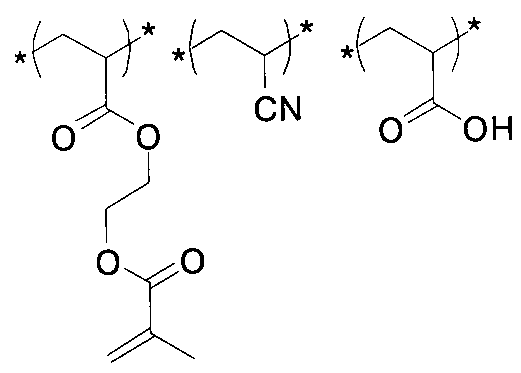
<実施例1>
[1.工程(X)]
両面銅張り板(ガラスエポキシ基板)をCZ処理(商品名:CZ-8100,メック株式会社製)し、銅表面を微細粗化した。
[1.工程(X)]
両面銅張り板(ガラスエポキシ基板)をCZ処理(商品名:CZ-8100,メック株式会社製)し、銅表面を微細粗化した。
[2.工程(Y)]
微細粗化した銅表面上にドライフィルムレジスト(DFR,商品名;RY3315,日立化成工業株式会社製)を真空ラミネーターにより、0.2MPaの圧力で70℃の条件にてラミネートした。ラミネート後、銅パターン形成部を中心波長365nmの露光機にて、70mJ/m2の条件でマスク露光した。その後、1%重曹水溶液にて現像して、水洗を行い、サブトラクティブ・エッチング用のレジストパターンを得た。
微細粗化した銅表面上にドライフィルムレジスト(DFR,商品名;RY3315,日立化成工業株式会社製)を真空ラミネーターにより、0.2MPaの圧力で70℃の条件にてラミネートした。ラミネート後、銅パターン形成部を中心波長365nmの露光機にて、70mJ/m2の条件でマスク露光した。その後、1%重曹水溶液にて現像して、水洗を行い、サブトラクティブ・エッチング用のレジストパターンを得た。
[3.工程(Z)]
次に、レジストパターンが形成されていない非レジスト部の銅がエッチングされるまで、得られた基板に45℃の40%酸化第二銅液をスプレー噴射した。その後、得られた基板を水洗した。
次に、レジストパターンが形成されていない非レジスト部の銅がエッチングされるまで、得られた基板に45℃の40%酸化第二銅液をスプレー噴射した。その後、得られた基板を水洗した。
[4.工程(W)]
次に、レジストパターンを剥離すために、45℃の4%NaOH水溶液に基板を60秒間浸漬した。その後、得られた基板を水洗し、1%硫酸に30秒間浸漬した。その後、再び水洗した。
次に、レジストパターンを剥離すために、45℃の4%NaOH水溶液に基板を60秒間浸漬した。その後、得られた基板を水洗し、1%硫酸に30秒間浸漬した。その後、再び水洗した。
[5.工程(A)]
次に、工程(W)で得られた基板に、電気的絶縁層として味の素ファインテクノ社製エポキシ系絶縁膜GX-13(膜厚40μm)を、真空ラミネーターにより0.2MPaの圧力で100~110℃の条件により接着して、絶縁膜を形成した。その後、180℃にて30分間加熱処理を行った。
次に、工程(W)で得られた基板に、電気的絶縁層として味の素ファインテクノ社製エポキシ系絶縁膜GX-13(膜厚40μm)を、真空ラミネーターにより0.2MPaの圧力で100~110℃の条件により接着して、絶縁膜を形成した。その後、180℃にて30分間加熱処理を行った。
[6.工程(B)]
(A)工程で得られた絶縁層に対して、CO2レーザにより、トップ径60μm、ボトム径50μmの、銅箔に到達するビアホールを所定の位置に形成した。
(A)工程で得られた絶縁層に対して、CO2レーザにより、トップ径60μm、ボトム径50μmの、銅箔に到達するビアホールを所定の位置に形成した。
[7.工程(C)]
続いて(B)工程にてビアホールが形成された面に対しデスミア処理を行った。
具体的には、コンディショナー液として水酸化ナトリウムと溶剤が含まれるコンディショナー水溶液を調製し、攪拌を加えながら75℃にて10分間浸漬処理することで、絶縁層表面に膨潤処理を行った。その後、50℃温水にて3分処理した後に、過マンガン酸カリウムを含む水酸化ナトリウム水溶液を用いて攪拌を加えながら85℃にて10分間浸漬することでデスミアの処理を行った。その後、50℃温水にて3分浸漬処理した後に、硫酸が含まれる中和処理水溶液液を用いて、攪拌を加えながら45℃にて5分間浸漬することで中和処理を行った。
このデスミア処理により、ビアホールの底部における絶縁層の残渣を除去した。これは、表面SEMによるBSE像(反射電子像)により確認された。
なお、デスミア処理後の絶縁層の表面粗さ(Ra)は、0.8μmであった。
続いて(B)工程にてビアホールが形成された面に対しデスミア処理を行った。
具体的には、コンディショナー液として水酸化ナトリウムと溶剤が含まれるコンディショナー水溶液を調製し、攪拌を加えながら75℃にて10分間浸漬処理することで、絶縁層表面に膨潤処理を行った。その後、50℃温水にて3分処理した後に、過マンガン酸カリウムを含む水酸化ナトリウム水溶液を用いて攪拌を加えながら85℃にて10分間浸漬することでデスミアの処理を行った。その後、50℃温水にて3分浸漬処理した後に、硫酸が含まれる中和処理水溶液液を用いて、攪拌を加えながら45℃にて5分間浸漬することで中和処理を行った。
このデスミア処理により、ビアホールの底部における絶縁層の残渣を除去した。これは、表面SEMによるBSE像(反射電子像)により確認された。
なお、デスミア処理後の絶縁層の表面粗さ(Ra)は、0.8μmであった。
[8.工程(D)]
まず、工程(D)で使用される樹脂層形成用積層フィルムを以下の方法にて作製した。
ポリマーA:10.5質量部、アセトン73.3質量部、メタノール33.9質量部、及びN,N-ジメチルアセトアミド4.8質量部を混合攪拌し、塗布液を調製した。
調製された塗布液を、スピンコートにて膜厚32μmのPET支持体上に、スピンコート法により塗布し、80℃にて20分乾燥して、厚さ0.5μmの樹脂層を備える樹脂層形成用積層フィルムを得た。
得られた積層フィルムを、工程(C)で得られたビアホールを有する絶縁層上に、所定の圧力(押圧)をかけながらラミネートし、積層体を得た。ラミネートの際の、圧力条件は、0.1MPa、0.2MPa、0.4MPa、0.7MPa、または、1.0MPaのいずれかである。また、ラミネートの際の樹脂層の温度は、60℃、90℃、120℃、または150℃のいずれかである。なお、圧力をかける時間(プレス時間)は30秒であった。
まず、工程(D)で使用される樹脂層形成用積層フィルムを以下の方法にて作製した。
ポリマーA:10.5質量部、アセトン73.3質量部、メタノール33.9質量部、及びN,N-ジメチルアセトアミド4.8質量部を混合攪拌し、塗布液を調製した。
調製された塗布液を、スピンコートにて膜厚32μmのPET支持体上に、スピンコート法により塗布し、80℃にて20分乾燥して、厚さ0.5μmの樹脂層を備える樹脂層形成用積層フィルムを得た。
得られた積層フィルムを、工程(C)で得られたビアホールを有する絶縁層上に、所定の圧力(押圧)をかけながらラミネートし、積層体を得た。ラミネートの際の、圧力条件は、0.1MPa、0.2MPa、0.4MPa、0.7MPa、または、1.0MPaのいずれかである。また、ラミネートの際の樹脂層の温度は、60℃、90℃、120℃、または150℃のいずれかである。なお、圧力をかける時間(プレス時間)は30秒であった。
[9.工程(E)]
工程(D)で得られた積層体中の樹脂層を常温(25℃)に冷やし、仮支持体であるPET支持体を積層体から剥離した。得られた積層体中においては、絶縁層上にだけ樹脂層が堆積していた。
なお、該工程後、光学顕微鏡にて面状検査を行い、シート品の転写不良が生じていないか、または、ビアホールと重なる部分の樹脂層が切り抜かれていないか、について検査した。検査において、問題がないサンプルのみ、以下の工程を実施した。
工程(D)で得られた積層体中の樹脂層を常温(25℃)に冷やし、仮支持体であるPET支持体を積層体から剥離した。得られた積層体中においては、絶縁層上にだけ樹脂層が堆積していた。
なお、該工程後、光学顕微鏡にて面状検査を行い、シート品の転写不良が生じていないか、または、ビアホールと重なる部分の樹脂層が切り抜かれていないか、について検査した。検査において、問題がないサンプルのみ、以下の工程を実施した。
[10.工程(K)]
得られた積層体に対して、三永電機製のUV露光機(型番:UVF-502S、ランプ:UXM-501MD)を用い、1.5mW/cm2の照射パワー(ウシオ電機製紫外線積算光量計UIT150-受光センサーUVD-S254で照射パワー測定)にて、254nmのUV光を500mJ照射させて、絶縁層表面に全面にわたりグラフトポリマーを生成させた。次に、攪拌した状態のアセトン中に得られた積層体を5分間浸漬し、続いて、蒸留水にて洗浄した。
以上のようにして、絶縁層に直接化学結合した樹脂層を形成した。
得られた積層体に対して、三永電機製のUV露光機(型番:UVF-502S、ランプ:UXM-501MD)を用い、1.5mW/cm2の照射パワー(ウシオ電機製紫外線積算光量計UIT150-受光センサーUVD-S254で照射パワー測定)にて、254nmのUV光を500mJ照射させて、絶縁層表面に全面にわたりグラフトポリマーを生成させた。次に、攪拌した状態のアセトン中に得られた積層体を5分間浸漬し、続いて、蒸留水にて洗浄した。
以上のようにして、絶縁層に直接化学結合した樹脂層を形成した。
[11.工程(F)]
ジエチレングリコールジエチルエーテル(和光純薬社製)40質量部、水40質量部、硝酸(和光純薬社製)20質量部、及び酢酸パラジウム(和光純薬社製)0.25質量部からなるパラジウム触媒液を調製し、このパラジウム触媒液に工程(K)で得られた積層体を5分間浸漬した後、水で洗浄を行った。
上記のようにして、めっき触媒が付与された積層体に対し、上村工業(株)製スルカップPGT(PGT-A、PGT-B、PGT-C)を使用した下記組成の無電解めっき浴を用い、無電解めっき温度26℃で、30分間無電解めっきを行った。得られた無電解銅めっき膜の厚みは、樹脂層上、ビアホールの側面上および底部上、共に、0.5μmであった。
無電解めっき液の原料は以下の通りである。
・蒸留水 79.2質量%
・PGT-A 9.0質量%
・PGT-B 6.0質量%
・PGT-C 3.5質量%
・ホルマリン(和光純薬:ホルムアルデヒド液) 2.3質量%
ジエチレングリコールジエチルエーテル(和光純薬社製)40質量部、水40質量部、硝酸(和光純薬社製)20質量部、及び酢酸パラジウム(和光純薬社製)0.25質量部からなるパラジウム触媒液を調製し、このパラジウム触媒液に工程(K)で得られた積層体を5分間浸漬した後、水で洗浄を行った。
上記のようにして、めっき触媒が付与された積層体に対し、上村工業(株)製スルカップPGT(PGT-A、PGT-B、PGT-C)を使用した下記組成の無電解めっき浴を用い、無電解めっき温度26℃で、30分間無電解めっきを行った。得られた無電解銅めっき膜の厚みは、樹脂層上、ビアホールの側面上および底部上、共に、0.5μmであった。
無電解めっき液の原料は以下の通りである。
・蒸留水 79.2質量%
・PGT-A 9.0質量%
・PGT-B 6.0質量%
・PGT-C 3.5質量%
・ホルマリン(和光純薬:ホルムアルデヒド液) 2.3質量%
得られた無電解銅めっき膜付積層体を150℃にて30分間加熱処理を行い、その後、加熱処理酸化皮膜を落とすために、10%硫酸にて脱脂した。
荏原ユージライト社製のCU-BRITE VFII-A、及びCU-BRITE VFII-Bを使用した以下の原料構成にて電気めっき液を調製し、これを用いて無電解銅めっきが付与された積層体に対し、40分間の電気めっきを行った。なお、電気めっきの際の電流値は0.3A/dm2であった。得られた電気銅めっき膜の厚みは絶縁膜上で25μm、ビアホールの底部上で50μmであった。
・蒸留水 80.20質量%
・硫酸銅5水和物(和光純薬) 16.06質量%
・濃硫酸 2.01質量%
・VFII-A 1.64質量%
・VFII-B 0.08質量%
・塩酸 0.01質量%
・蒸留水 80.20質量%
・硫酸銅5水和物(和光純薬) 16.06質量%
・濃硫酸 2.01質量%
・VFII-A 1.64質量%
・VFII-B 0.08質量%
・塩酸 0.01質量%
上記工程により、層間が電気的に接続されたフィルドビアを有する多層配線基板を作製した。
得られた多層配線基板上の銅薄膜に対して、上記工程(Y)から工程(W)の処理を再度行い、図8(A)のような50μmφのブラインドビア100ヶ所が接続されたビアチェーン(ビアホールのデイジー・チェーン)を、10ユニットずつ形成した。なお、図8(A)は、実施例1で得られたビアチェーンを表す模式的断面図である。
<実施例2>
上記工程(D)において、樹脂層の厚さを0.5μmから2.5μmに変更した以外は、実施例1と同様の方法により多層配線基板およびビアチェーンを作製した。
実施例2で得られたビアチェーンの模式的断面図は、図8(A)で示される。
上記工程(D)において、樹脂層の厚さを0.5μmから2.5μmに変更した以外は、実施例1と同様の方法により多層配線基板およびビアチェーンを作製した。
実施例2で得られたビアチェーンの模式的断面図は、図8(A)で示される。
<実施例3>
上記工程(D)において、ポリマーAの代わりにポリマーBを使用し、工程(F)において、パラジウム触媒液の代わりに0.5質量%硝酸銀水溶液を使用した以外は、実施例1と同様の方法により多層配線基板およびビアチェーンを作製した。
実施例3で得られたビアチェーンの模式的断面図は、図8(A)で示される。
上記工程(D)において、ポリマーAの代わりにポリマーBを使用し、工程(F)において、パラジウム触媒液の代わりに0.5質量%硝酸銀水溶液を使用した以外は、実施例1と同様の方法により多層配線基板およびビアチェーンを作製した。
実施例3で得られたビアチェーンの模式的断面図は、図8(A)で示される。
<実施例4>
上記実施例1の工程(D)の前において、以下の工程(G)および工程(H)を実施して、その後、得られた密着補助層を備える積層体に対して、実施例1の工程(D)から工程(F)を実施して、密着補助層と樹脂層とを備える多層配線基板およびビアチェーンを作製した。
図8(B)は、実施例4で得られたビアチェーンを表す模式的断面図であり、図8(A)と比較して、密着補助層が含まれている。
上記実施例1の工程(D)の前において、以下の工程(G)および工程(H)を実施して、その後、得られた密着補助層を備える積層体に対して、実施例1の工程(D)から工程(F)を実施して、密着補助層と樹脂層とを備える多層配線基板およびビアチェーンを作製した。
図8(B)は、実施例4で得られたビアチェーンを表す模式的断面図であり、図8(A)と比較して、密着補助層が含まれている。
[工程(G)]
まず、工程(G)で使用される密着補助層形成用積層フィルムを以下の方法にて作製した。
まず、工程(G)で使用される密着補助層形成用積層フィルムを以下の方法にて作製した。
(重合開始剤を含有する絶縁性組成物)
ビスフェノールA型エポキシ樹脂(エポキシ当量185、油化シェルエポキシ(株)製エピコート828)20質量部、クレゾールノボラック型エポキシ樹脂(エポキシ当量215、大日本インキ化学工業(株)製エピクロンN-673)45質量部、フェノールノボラック樹脂(フェノール性水酸基当量105、大日本インキ化学工業(株)製フェノライト)20質量部を、エチルジグリコールアセテート20部、及びソルベントナフサ20部に、攪拌しながら加熱溶解させ室温まで冷却した後、そこへエピコート828とビスフェノールSとからなるフェノキシ樹脂のシクロヘキサノンワニス(油化シェルエポキシ(株)製YL6747H30、不揮発分30質量%、重量平均分子量47000)30質量部、2-フェニル-4,5-ビス(ヒドロキシメチル)イミダゾール0.8質量部、微粉砕シリカ2質量部、シリコン系消泡剤(信越シリコン社製、商品名:KS604)0.5質量部を添加し、更にこの混合物中に、下記の方法で合成した重合開始剤(重合開始ポリマーP)を10部添加し、重合開始剤を含有する絶縁性組成物を得た。
ビスフェノールA型エポキシ樹脂(エポキシ当量185、油化シェルエポキシ(株)製エピコート828)20質量部、クレゾールノボラック型エポキシ樹脂(エポキシ当量215、大日本インキ化学工業(株)製エピクロンN-673)45質量部、フェノールノボラック樹脂(フェノール性水酸基当量105、大日本インキ化学工業(株)製フェノライト)20質量部を、エチルジグリコールアセテート20部、及びソルベントナフサ20部に、攪拌しながら加熱溶解させ室温まで冷却した後、そこへエピコート828とビスフェノールSとからなるフェノキシ樹脂のシクロヘキサノンワニス(油化シェルエポキシ(株)製YL6747H30、不揮発分30質量%、重量平均分子量47000)30質量部、2-フェニル-4,5-ビス(ヒドロキシメチル)イミダゾール0.8質量部、微粉砕シリカ2質量部、シリコン系消泡剤(信越シリコン社製、商品名:KS604)0.5質量部を添加し、更にこの混合物中に、下記の方法で合成した重合開始剤(重合開始ポリマーP)を10部添加し、重合開始剤を含有する絶縁性組成物を得た。
(重合開始ポリマーPの合成)
300mlの三口フラスコに、プロピレングリコールモノメチルエーテル(MFG)30gを加え75℃に加熱した。そこに、[2-(Acryloyloxy)ethyl](4-benzoylbenzyl)dimethyl ammonium bromide(8.1g)と、2-Hydroxyethylmethacrylate(9.9g)と、isopropylmethaacrylate(13.5g)と、ジメチル-2,2’-アゾビス(2-メチルプロピオネート)0.43gと、MFG30gと、の溶液を2.5時間かけて滴下した。その後、反応温度を80℃に上げ、更に2時間反応させ、重合開始基を有するポリマーPを得た。
300mlの三口フラスコに、プロピレングリコールモノメチルエーテル(MFG)30gを加え75℃に加熱した。そこに、[2-(Acryloyloxy)ethyl](4-benzoylbenzyl)dimethyl ammonium bromide(8.1g)と、2-Hydroxyethylmethacrylate(9.9g)と、isopropylmethaacrylate(13.5g)と、ジメチル-2,2’-アゾビス(2-メチルプロピオネート)0.43gと、MFG30gと、の溶液を2.5時間かけて滴下した。その後、反応温度を80℃に上げ、更に2時間反応させ、重合開始基を有するポリマーPを得た。
(シリカ微粒子の分散)
上記重合開始剤を含有する絶縁性組成物100重量部に、MEK分散シリカゾル(商品名;MEK-ST-L,SiO2 20wt%,粒子径70~100nm、日産化学工業株式会社製)を10重量部添加し、25℃にて30混合攪拌し、塗布液を調製した。
上記重合開始剤を含有する絶縁性組成物100重量部に、MEK分散シリカゾル(商品名;MEK-ST-L,SiO2 20wt%,粒子径70~100nm、日産化学工業株式会社製)を10重量部添加し、25℃にて30混合攪拌し、塗布液を調製した。
調製された塗布液を、スピンコートにて膜厚32μmのPET支持体上に、スピンコート法により塗布し、80℃にて20分乾燥して、厚さ1.5μmの密着補助層を備える密着補助層形成用積層フィルムを得た。
得られた積層フィルムを、工程(C)で得られたビアホールを有する絶縁層上に、所定の圧力(押圧)をかけながらラミネートし、積層体を得た。ラミネートの際の、圧力条件は、0.1MPa、0.2MPa、0.4MPa、0.7MPa、または、1.0MPaのいずれかである。また、ラミネートの際の密着補助層の温度は、60℃、90℃、120℃、または150℃のいずれかである。なお、圧力をかける時間(プレス時間)は30秒であった。
得られた積層フィルムを、工程(C)で得られたビアホールを有する絶縁層上に、所定の圧力(押圧)をかけながらラミネートし、積層体を得た。ラミネートの際の、圧力条件は、0.1MPa、0.2MPa、0.4MPa、0.7MPa、または、1.0MPaのいずれかである。また、ラミネートの際の密着補助層の温度は、60℃、90℃、120℃、または150℃のいずれかである。なお、圧力をかける時間(プレス時間)は30秒であった。
[工程(H)]
工程(G)で得られた積層体中の密着補助層を常温(25℃)に冷やし、仮支持体であるPET支持体を積層体から剥離した。得られた積層体中においては、絶縁層上にだけ密着補助層が堆積していた。
なお、該工程後、光学顕微鏡にて面状検査を行い、シート品の転写不良が生じていないか、または、ビアホールと重なる部分の密着補助層が切り抜かれていないか、について検査した。検査において、問題がないサンプルのみ、工程(D)を実施した。
工程(G)で得られた積層体中の密着補助層を常温(25℃)に冷やし、仮支持体であるPET支持体を積層体から剥離した。得られた積層体中においては、絶縁層上にだけ密着補助層が堆積していた。
なお、該工程後、光学顕微鏡にて面状検査を行い、シート品の転写不良が生じていないか、または、ビアホールと重なる部分の密着補助層が切り抜かれていないか、について検査した。検査において、問題がないサンプルのみ、工程(D)を実施した。
<比較例1>
特開2010-157590号の段落[0121]~[0133]に記載の実施例1で使用された材料を使用して、該実施例1に記載の方法で、上記実施例1~3と同様の構造の多層配線基板を作製した。
また、得られた多層配線基板に対して、実施例1~3と同様に工程(Y)~(W)を実施して、図8(A)のような50μmφのブラインドビア100ヶ所が接続されたビアチェーンを、10ユニットずつ形成した。
特開2010-157590号の段落[0121]~[0133]に記載の実施例1で使用された材料を使用して、該実施例1に記載の方法で、上記実施例1~3と同様の構造の多層配線基板を作製した。
また、得られた多層配線基板に対して、実施例1~3と同様に工程(Y)~(W)を実施して、図8(A)のような50μmφのブラインドビア100ヶ所が接続されたビアチェーンを、10ユニットずつ形成した。
<表面銅箔(金属層)の引き剥がし強度(90°ピール強度)>
実施例1~4、および比較例1で得られたビア基板(積層体)に対して、JIS C 6481(1996年)プリント配線板用銅張積層板試験に記載の方法にて表層銅箔の90°引き剥がし試験を行った。試験機は(株)島津製作所製のオートグラフAGS-Jを使用し、引き剥がす銅箔の幅は10mm、引き剥がし速度は毎分50mm、測定数はN=5とし、その平均値を算出した。その平均値を算出したが、実施例1~4、および比較例1のいずれも0.7から0.8N/mmと実用的な値を示していた。
なお、実用上の点から、ピール強度は0.6N/mm以上であることが必要である。
実施例1~4、および比較例1で得られたビア基板(積層体)に対して、JIS C 6481(1996年)プリント配線板用銅張積層板試験に記載の方法にて表層銅箔の90°引き剥がし試験を行った。試験機は(株)島津製作所製のオートグラフAGS-Jを使用し、引き剥がす銅箔の幅は10mm、引き剥がし速度は毎分50mm、測定数はN=5とし、その平均値を算出した。その平均値を算出したが、実施例1~4、および比較例1のいずれも0.7から0.8N/mmと実用的な値を示していた。
なお、実用上の点から、ピール強度は0.6N/mm以上であることが必要である。
<膜物性の評価(その1)>
上記で使用したポリマーAから構成される樹脂層(以後、適宜樹脂層A)、ポリマーBから構成される樹脂層(以後、適宜樹脂層B)、密着補助層のヤング率(貯蔵弾性率)を動的粘弾性測定装置(DMS6100,SII製)にて、1Hzの周波数で測定した。
なお、樹脂層Aのガラス転移温度は35℃であり、ガラス転移温度~ガラス転移温度+60℃の温度範囲におけるヤング率は2.0×10⁵~6.0×10⁷MPaであり、破断点伸度は70%であった。
なお、樹脂層Bのガラス転移温度は75℃であり、ガラス転移温度~ガラス転移温度+60℃の温度範囲におけるヤング率は5.0×10⁵~1.0×10⁸MPaであり、破断点伸度は25%であった。
なお、密着補助層のガラス転移温度は105℃であり、ガラス転移温度~ガラス転移温度+60℃の温度範囲におけるヤング率は8.0×10⁵~1.0×10⁸MPaであり、破断点伸度は15%であった。
上記で使用したポリマーAから構成される樹脂層(以後、適宜樹脂層A)、ポリマーBから構成される樹脂層(以後、適宜樹脂層B)、密着補助層のヤング率(貯蔵弾性率)を動的粘弾性測定装置(DMS6100,SII製)にて、1Hzの周波数で測定した。
なお、樹脂層Aのガラス転移温度は35℃であり、ガラス転移温度~ガラス転移温度+60℃の温度範囲におけるヤング率は2.0×10⁵~6.0×10⁷MPaであり、破断点伸度は70%であった。
なお、樹脂層Bのガラス転移温度は75℃であり、ガラス転移温度~ガラス転移温度+60℃の温度範囲におけるヤング率は5.0×10⁵~1.0×10⁸MPaであり、破断点伸度は25%であった。
なお、密着補助層のガラス転移温度は105℃であり、ガラス転移温度~ガラス転移温度+60℃の温度範囲におけるヤング率は8.0×10⁵~1.0×10⁸MPaであり、破断点伸度は15%であった。
<膜物性の評価(その2)>
実施例1および2における、樹脂層Aと絶縁層との単位面積当たりの界面剥離強度σ(A1)、樹脂層Aと仮支持体との単位面積当たりの界面剥離強度σ(B1)と、樹脂層Aの破断応力σ(C1)を、サイカス(メコン株式会社製)によって、測定した。
界面剥離強度σ(A1)は200MPaで、界面剥離強度σ(B1)は140MPaで、破断応力σ(C1)は75MPaであり、σ(A1)>σ(B1)>σ(C1)の関係を満たしていた。
実施例3における、樹脂層Bと絶縁層との単位面積当たりの界面剥離強度σ(A1)は220MPaで、樹脂層Bと仮支持体との単位面積当たりの界面剥離強度σ(B1)は160MPaで、樹脂層Bの破断応力σ(C1)は100MPaであり、σ(A1)>σ(B1)>σ(C1)の関係を満たしていた。
実施例4における、密着補助層と絶縁層の単位面積当たりの界面剥離強度σ(A2)は180MPaで、密着補助層と仮支持体の単位面積当たりの界面剥離強度σ(B2)は130MPaで、密着補助層の破断応力σ(C2)は80MPaで、σ(A2)>σ(B2)>σ(C2)の関係を満たしていた。
また、実施例4における、樹脂層Aと密着補助層の単位面積当たりの界面剥離強度σ(A3)は180MPaで、樹脂層Aと仮支持体との単位面積当たりの界面剥離強度σ(B1)は130MPaで、樹脂層Aの破断応力σ(C1)は80MPaであり、σ(A2),σ(A3)>σ(B1),σ(B2)>σ(C1),σ(C2)の関係を満たしていた。
実施例1および2における、樹脂層Aと絶縁層との単位面積当たりの界面剥離強度σ(A1)、樹脂層Aと仮支持体との単位面積当たりの界面剥離強度σ(B1)と、樹脂層Aの破断応力σ(C1)を、サイカス(メコン株式会社製)によって、測定した。
界面剥離強度σ(A1)は200MPaで、界面剥離強度σ(B1)は140MPaで、破断応力σ(C1)は75MPaであり、σ(A1)>σ(B1)>σ(C1)の関係を満たしていた。
実施例3における、樹脂層Bと絶縁層との単位面積当たりの界面剥離強度σ(A1)は220MPaで、樹脂層Bと仮支持体との単位面積当たりの界面剥離強度σ(B1)は160MPaで、樹脂層Bの破断応力σ(C1)は100MPaであり、σ(A1)>σ(B1)>σ(C1)の関係を満たしていた。
実施例4における、密着補助層と絶縁層の単位面積当たりの界面剥離強度σ(A2)は180MPaで、密着補助層と仮支持体の単位面積当たりの界面剥離強度σ(B2)は130MPaで、密着補助層の破断応力σ(C2)は80MPaで、σ(A2)>σ(B2)>σ(C2)の関係を満たしていた。
また、実施例4における、樹脂層Aと密着補助層の単位面積当たりの界面剥離強度σ(A3)は180MPaで、樹脂層Aと仮支持体との単位面積当たりの界面剥離強度σ(B1)は130MPaで、樹脂層Aの破断応力σ(C1)は80MPaであり、σ(A2),σ(A3)>σ(B1),σ(B2)>σ(C1),σ(C2)の関係を満たしていた。
<仮支持体剥離後のラミネートの形成性>
実施例1から実施例4について、上記工程(D)または工程(H)における仮支持体剥離後の、ビアホールと重なる、シートの不要領域切取り除去の得率を、樹脂層A、樹脂層B、密着補助層、各々について調べた。
具体的には、実施例に示したように、各積層フィルムのラミネートは、温度4点、押圧5点の組み合わせ条件の総計、20条件で行なった。検査したビアホールの個数は各441個であり、検査は電子顕微鏡にて仮支持体剥離後の積層体表面を観察した。各積層フィルムをラミネートして、仮支持体を剥離した後に、何個のビアホールが樹脂層A、樹脂層B、または密着補助層などによる閉塞なしに、残存しているかを数え、切り抜き除去率(残存しているビアホール/441)を計算した。該切り抜き除去率が高いほど、ビアホールが残存していることを意味する。
切抜き除去率が100%のものを○、20%以上100%未満のものを△、20%未満のものを×と判定し、ラミ温度におけるシート品のヤング率(貯蔵弾性率)と、ラミ押圧に対してマッピングを行なった。実施例1~4の結果を表1に、マッピングの結果を表7に示す。実用上、「○」であることが必要である。なお、表1中の実施例4の結果は、密着補助層形成用積層フィルムを使用して、密着補助層の切り抜き除去率を測定した結果である。実施例4における樹脂層の切り抜き除去率の結果は、実施例1と同じであった。
また、切抜き除去がOK品(ビアホールが残存している)のSEM写真を図4に、NG品(ビアホールが各種層により閉塞している)のSEM写真を図5および6に示す。なお、図5は各層の一部が残存している場合を示し、図6はビアホールが各層によって閉塞している場合を示す。
実施例1から実施例4について、上記工程(D)または工程(H)における仮支持体剥離後の、ビアホールと重なる、シートの不要領域切取り除去の得率を、樹脂層A、樹脂層B、密着補助層、各々について調べた。
具体的には、実施例に示したように、各積層フィルムのラミネートは、温度4点、押圧5点の組み合わせ条件の総計、20条件で行なった。検査したビアホールの個数は各441個であり、検査は電子顕微鏡にて仮支持体剥離後の積層体表面を観察した。各積層フィルムをラミネートして、仮支持体を剥離した後に、何個のビアホールが樹脂層A、樹脂層B、または密着補助層などによる閉塞なしに、残存しているかを数え、切り抜き除去率(残存しているビアホール/441)を計算した。該切り抜き除去率が高いほど、ビアホールが残存していることを意味する。
切抜き除去率が100%のものを○、20%以上100%未満のものを△、20%未満のものを×と判定し、ラミ温度におけるシート品のヤング率(貯蔵弾性率)と、ラミ押圧に対してマッピングを行なった。実施例1~4の結果を表1に、マッピングの結果を表7に示す。実用上、「○」であることが必要である。なお、表1中の実施例4の結果は、密着補助層形成用積層フィルムを使用して、密着補助層の切り抜き除去率を測定した結果である。実施例4における樹脂層の切り抜き除去率の結果は、実施例1と同じであった。
また、切抜き除去がOK品(ビアホールが残存している)のSEM写真を図4に、NG品(ビアホールが各種層により閉塞している)のSEM写真を図5および6に示す。なお、図5は各層の一部が残存している場合を示し、図6はビアホールが各層によって閉塞している場合を示す。
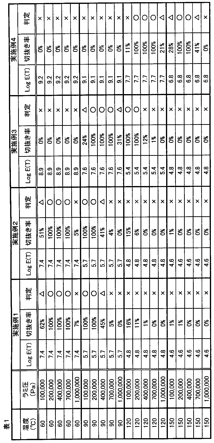
マッピングの結果から、図7に示す太線枠内において、ビアホールの形成が良好であることが分かった。有限要素解析によって、応力-歪み特性の計算を行なったが、類似の結果を得た。マッピングと応力解析の結果をもとに、枠線の直線近似を行なった結果、
i) P=0.3×10⁶Log(E(T))-1.4×10⁶
ii) P=0.06×10⁶Log(E(T))-0.3×10⁶
iii) Log(E(T))=5.2
iv) Log(E(T))=8
i)からiv)に囲まれる領域がビアホール形成可能な領域(シート切抜きが可能な領域)であることが分かり、シート品のヤング率とラミネート時の圧力(押圧)を管理しておけば、ビアホールの形成を制御できることが分かった。
i) P=0.3×10⁶Log(E(T))-1.4×10⁶
ii) P=0.06×10⁶Log(E(T))-0.3×10⁶
iii) Log(E(T))=5.2
iv) Log(E(T))=8
i)からiv)に囲まれる領域がビアホール形成可能な領域(シート切抜きが可能な領域)であることが分かり、シート品のヤング率とラミネート時の圧力(押圧)を管理しておけば、ビアホールの形成を制御できることが分かった。
<比較例2>
実施例1における[8.工程(D)]における、ラミネートの際の圧力条件を0.15MPaに、樹脂層の温度を110℃にした以外は、実施例1と同様の手順で、多層配線基板およびビアチェーンの作製を行った。
しかしながら、比較例2においては、上記仮支持体剥離後の切抜き除去率が「×」であり、所望の多層配線基板を得ることはできなかった。
実施例1における[8.工程(D)]における、ラミネートの際の圧力条件を0.15MPaに、樹脂層の温度を110℃にした以外は、実施例1と同様の手順で、多層配線基板およびビアチェーンの作製を行った。
しかしながら、比較例2においては、上記仮支持体剥離後の切抜き除去率が「×」であり、所望の多層配線基板を得ることはできなかった。
<ビアチェーンの初期導通率>
実施例1~4、および、比較例1で作製したビアチェーンの接続信頼性を評価するために、配線形成直後の導通不良率(初期不良)を調べた。ここでは導通しなかったものを、導通不良として判断した。その結果を、下表2に記す。なお、実施例1~4においては、表2中の条件1~5の条件で作製したビアチェーンに関して、評価した。
表2中、温度(T)は、ラミネート時の樹脂層または密着補助層の温度を意味し、押圧(P)は樹脂層形成用積層フィルムまたは密着補助層形成用積層フィルムに加えられる圧力を意味する。なお、実用上、導通不良率は、30%以下であることが望ましい。表2中の実施例4においては、樹脂層Aおよび密着補助層のいずれの切抜き除去率は100%であった。
本発明の製造方法によってビア形成したものは、比較例に比べてビアチェーンの導通が非常に良いことが分かった。
一方、比較例の故障品の導通不良を調べたところ、図9のSEM写真のようなフィリング不良が多発していることが分かった。比較例においては、SEM写真より、壁面からのめっき成長が低い、または不安定なことが分かった。これは、液状組成物を用いて樹脂層を形成していることに起因していると予想できる。
実施例1~4、および、比較例1で作製したビアチェーンの接続信頼性を評価するために、配線形成直後の導通不良率(初期不良)を調べた。ここでは導通しなかったものを、導通不良として判断した。その結果を、下表2に記す。なお、実施例1~4においては、表2中の条件1~5の条件で作製したビアチェーンに関して、評価した。
表2中、温度(T)は、ラミネート時の樹脂層または密着補助層の温度を意味し、押圧(P)は樹脂層形成用積層フィルムまたは密着補助層形成用積層フィルムに加えられる圧力を意味する。なお、実用上、導通不良率は、30%以下であることが望ましい。表2中の実施例4においては、樹脂層Aおよび密着補助層のいずれの切抜き除去率は100%であった。
本発明の製造方法によってビア形成したものは、比較例に比べてビアチェーンの導通が非常に良いことが分かった。
一方、比較例の故障品の導通不良を調べたところ、図9のSEM写真のようなフィリング不良が多発していることが分かった。比較例においては、SEM写真より、壁面からのめっき成長が低い、または不安定なことが分かった。これは、液状組成物を用いて樹脂層を形成していることに起因していると予想できる。
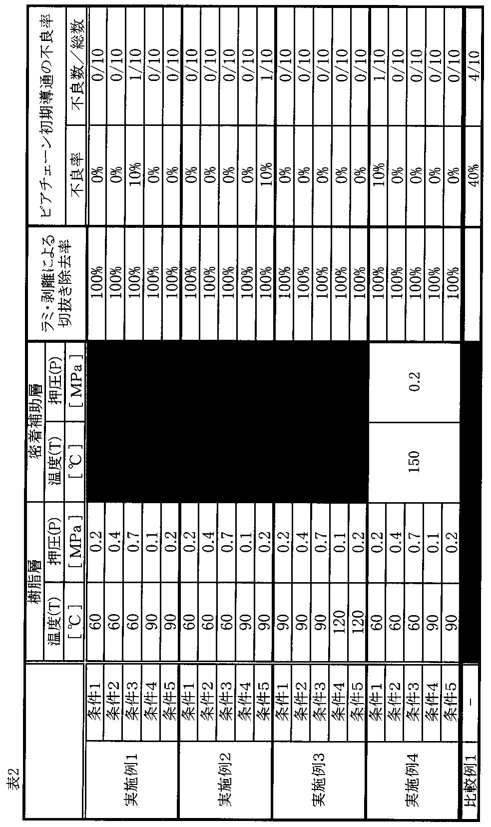
10:配線基板
12:基板
14:金属配線
16:絶縁層
18:ビアホール
20:樹脂層
22:仮支持体
24:樹脂層形成用積層フィルム
26、34、36:積層体
28:金属膜
30:密着補助層
32:密着補助層用積層フィルム
12:基板
14:金属配線
16:絶縁層
18:ビアホール
20:樹脂層
22:仮支持体
24:樹脂層形成用積層フィルム
26、34、36:積層体
28:金属膜
30:密着補助層
32:密着補助層用積層フィルム
Claims (10)
- (A)金属配線を備える配線基板の表面に、絶縁層を形成する工程と
(B)前記絶縁層を貫通し、前記金属配線に達するようにビアホールを形成する工程と、
(C)前記工程(B)後に、デスミア処理を行う工程と、
(D)前記工程(C)後に、仮支持体と、前記仮支持体上にめっき触媒またはその前駆体と相互作用を形成する官能基、及び、重合性基を含有するポリマーを含む樹脂層とを備える樹脂層形成用積層フィルムを、前記絶縁層上に、前記樹脂層とデスミア処理が施された前記絶縁層とが接するようにラミネートし、積層体を得る工程と、
(E)前記工程(D)後に、前記積層体から前記仮支持体を剥離する工程と、
(F)前記工程(E)後に、前記ビアホールの壁面および前記樹脂層にめっき触媒またはその前駆体を付与し、めっきを行う工程と、を備え、
前記工程(D)において、ラミネートする際の前記樹脂層の温度Tが、前記樹脂層のガラス転移温度以上ガラス転移温度+60℃以下であり、前記温度Tにおける前記樹脂層のヤング率E(T)が0.16×10⁶~100×106Paで、前記樹脂層の破断点伸度が100%以下であり、
前記樹脂層形成用積層フィルムをラミネートする際に、前記樹脂層形成用積層フィルムに加えられる圧力Pと、Log(E(T))とが、図3に示される、下記式(I)~(IV)で表される直線で囲まれた範囲に存在する、多層配線基板の製造方法。
式(I) Log(E(T))=5.2
式(II) Log(E(T))=8
式(III) P=0.3×10⁶(Log(E(T))-1.4×10⁶
式(IV) P=0.06×10⁶(Log(E(T))-0.3×10⁶ - 前記工程(E)において、前記樹脂層の温度が0~40℃であり、
前記樹脂層と前記絶縁層との単位面積当たりの界面剥離強度σ(A1)と、前記樹脂層と前記仮支持体との単位面積当たりの界面剥離強度σ(B1)と、前記樹脂層の破断応力σ(C1)とが、以下の関係を満足する、請求項1に記載の多層配線基板の製造方法。
σ(A1)>σ(B1)>σ(C1) - 前記樹脂層の厚みが、0.05~3.0μmである、請求項1または2に記載の多層配線基板の製造方法。
- 前記工程(E)と前記工程(F)との間に、前記樹脂層に対してエネルギー付与を行う工程を備える、請求項1~3のいずれかに記載の多層配線基板の製造方法。
- 前記工程(D)および前記工程(E)の代わりに、以下の工程(G)から工程(J)をこの順に実施する、請求項1に記載の多層配線基板の製造方法。
(G)前記工程(C)後に、仮支持体と、前記仮支持体上に密着補助層とを備える密着補助層形成用積層フィルムを、前記絶縁層上に、前記密着補助層とデスミア処理が施された前記絶縁層とが接するようにラミネートし、積層体を得る工程
(H)前記工程(G)後に、前記積層体から前記仮支持体を剥離する工程
(I)前記工程(H)後に、仮支持体と、前記仮支持体上にめっき触媒またはその前駆体と相互作用を形成する官能基、及び、重合性基を含有するポリマーを含む樹脂層とを備える樹脂層形成用積層フィルムを、前記密着補助層上に、前記樹脂層と前記密着補助層とが接するようにラミネートし、積層体を得る工程
(J)前記工程(I)後に、前記積層体から前記仮支持体を剥離する工程
なお、前記工程(G)および前記工程(I)において、ラミネートする際の前記密着補助層および前記樹脂層の温度Tが、前記密着補助層および前記樹脂層のそれぞれのガラス転移温度以上ガラス転移温度+60℃以下であり、前記温度Tにおける前記密着補助層および前記樹脂層のヤング率E(T)が0.16×10⁶~100×106Paで、前記密着補助層および前記樹脂層の破断点伸度が100%以下であり、
前記密着補助層形成用積層フィルムおよび前記樹脂層形成用積層フィルムをラミネートする際に、前記密着補助層形成用積層フィルムおよび前記樹脂層形成用積層フィルムに加えられる圧力Pと、Log(E(T))とが、図3に示される、下記式(I)~(IV)で表される直線で囲まれた範囲に存在する。
式(I) Log(E(T))=5.2
式(II) Log(E(T))=8
式(III) P=0.3×10⁶(Log(E(T))-1.4×10⁶
式(IV) P=0.06×10⁶(Log(E(T))-0.3×10⁶ - 前記工程(J)と前記工程(F)との間に、前記樹脂層に対してエネルギー付与を行う工程を備える、請求項5に記載の多層配線基板の製造方法。
- 前記密着補助層が重合開始剤を含有する、請求項5または6に記載の多層配線基板の製造方法。
- 前記めっき触媒またはその前駆体が、Pd、Ag、またはCuを含む化合物である、請求項1~7のいずれかに記載の多層配線基板の製造方法。
- 前記めっき触媒またはその前駆体と相互作用を形成する官能基が、シアノ基またはカルボン酸基である、請求項1~8のいずれかに記載の多層配線基板の製造方法。
- 請求項1~9のいずれかに記載の多層配線基板の製造方法によって得られる多層配線基板。
Applications Claiming Priority (2)
| Application Number | Priority Date | Filing Date | Title |
|---|---|---|---|
| JP2010203582A JP2012060031A (ja) | 2010-09-10 | 2010-09-10 | 多層配線基板の製造方法 |
| JP2010-203582 | 2010-09-10 |
Publications (1)
| Publication Number | Publication Date |
|---|---|
| WO2012033152A1 true WO2012033152A1 (ja) | 2012-03-15 |
Family
ID=45810748
Family Applications (1)
| Application Number | Title | Priority Date | Filing Date |
|---|---|---|---|
| PCT/JP2011/070437 Ceased WO2012033152A1 (ja) | 2010-09-10 | 2011-09-08 | 多層配線基板の製造方法 |
Country Status (2)
| Country | Link |
|---|---|
| JP (1) | JP2012060031A (ja) |
| WO (1) | WO2012033152A1 (ja) |
Cited By (1)
| Publication number | Priority date | Publication date | Assignee | Title |
|---|---|---|---|---|
| US20140118964A1 (en) * | 2012-11-01 | 2014-05-01 | Ajinomoto Co., Inc. | Method for producing printed wiring board |
Families Citing this family (2)
| Publication number | Priority date | Publication date | Assignee | Title |
|---|---|---|---|---|
| JP2016219507A (ja) * | 2015-05-15 | 2016-12-22 | パナソニック株式会社 | 電子デバイスの製造方法および電子デバイス |
| KR102916485B1 (ko) | 2024-01-15 | 2026-01-21 | 국립경국대학교 산학협력단 | 레이저를 이용한 선택적 가교층 형성에 의한 무전해 도금 전극 형성 방법 |
Citations (3)
| Publication number | Priority date | Publication date | Assignee | Title |
|---|---|---|---|---|
| JPH06148877A (ja) * | 1992-08-07 | 1994-05-27 | Hitachi Chem Co Ltd | フォトビア形成用感光性エレメント及び多層配線板の製造法 |
| JP2001308536A (ja) * | 2000-04-27 | 2001-11-02 | Kyocera Corp | 多層配線基板およびその製造方法 |
| JP2010157590A (ja) * | 2008-12-26 | 2010-07-15 | Fujifilm Corp | 多層配線基板の製造方法 |
-
2010
- 2010-09-10 JP JP2010203582A patent/JP2012060031A/ja not_active Ceased
-
2011
- 2011-09-08 WO PCT/JP2011/070437 patent/WO2012033152A1/ja not_active Ceased
Patent Citations (3)
| Publication number | Priority date | Publication date | Assignee | Title |
|---|---|---|---|---|
| JPH06148877A (ja) * | 1992-08-07 | 1994-05-27 | Hitachi Chem Co Ltd | フォトビア形成用感光性エレメント及び多層配線板の製造法 |
| JP2001308536A (ja) * | 2000-04-27 | 2001-11-02 | Kyocera Corp | 多層配線基板およびその製造方法 |
| JP2010157590A (ja) * | 2008-12-26 | 2010-07-15 | Fujifilm Corp | 多層配線基板の製造方法 |
Cited By (2)
| Publication number | Priority date | Publication date | Assignee | Title |
|---|---|---|---|---|
| US20140118964A1 (en) * | 2012-11-01 | 2014-05-01 | Ajinomoto Co., Inc. | Method for producing printed wiring board |
| US9516765B2 (en) * | 2012-11-01 | 2016-12-06 | Ajinomoto Co., Inc. | Method for producing printed wiring board |
Also Published As
| Publication number | Publication date |
|---|---|
| JP2012060031A (ja) | 2012-03-22 |
Similar Documents
| Publication | Publication Date | Title |
|---|---|---|
| JP5419441B2 (ja) | 多層配線基板の形成方法 | |
| JP5079396B2 (ja) | 導電性物質吸着性樹脂フイルム、導電性物質吸着性樹脂フイルムの製造方法、それを用いた金属層付き樹脂フイルム、及び、金属層付き樹脂フイルムの製造方法 | |
| WO2012111375A1 (ja) | 多層基板の製造方法、デスミア処理方法 | |
| JP4850487B2 (ja) | プリント配線板用積層体、それを用いたプリント配線板、プリント配線基板の作製方法、電気部品、電子部品、および、電気機器 | |
| WO2017026501A1 (ja) | 多層プリント配線板の製造方法、接着層付き金属箔、金属張積層板、多層プリント配線板 | |
| JP2012084640A (ja) | 積層体の製造方法 | |
| US20080093111A1 (en) | Multilayer wiring board and method of manufacturing the same | |
| TWI610814B (zh) | 附孔積層體的製造方法、附孔積層體、多層基板的製造方法及底層形成用組成物 | |
| WO2010073882A1 (ja) | 多層配線基板の製造方法 | |
| TW201930075A (zh) | 附設絕緣性樹脂層之銅箔 | |
| TW201309146A (zh) | 多層基板的製造方法、多層基板以及半導體封裝基板 | |
| WO2012033152A1 (ja) | 多層配線基板の製造方法 | |
| JP2012209392A (ja) | パターン状金属膜を有する積層体の製造方法、被めっき層形成用組成物 | |
| JP4505284B2 (ja) | 多層配線板の製造方法 | |
| WO2012029865A1 (ja) | 多層配線基板の製造方法 | |
| JP2005005458A (ja) | 多層配線板の製造方法 | |
| JP2011111602A (ja) | 絶縁性樹脂、絶縁性樹脂層形成用組成物、積層体、表面金属膜材料の作製方法、金属パターン材料の作製方法、配線基板の作製方法、電子部品、及び、半導体素子 | |
| JP2008258211A (ja) | 多層配線基板の製造方法及び多層配線基板 | |
| JP2009006698A (ja) | 両面金属膜付きフィルムの製造方法、及び両面金属膜付きフィルム | |
| JP2013102050A (ja) | 穴付き積層体およびその製造方法、多層基板およびその製造方法、下地層形成用組成物 | |
| JP2013041928A (ja) | 穴付き積層体の製造方法、多層基板の製造方法、穴形成方法 | |
| WO2012032905A1 (ja) | 被めっき層形成用組成物、金属パターン材料の製造方法、および、新規ポリマー | |
| JP2012209387A (ja) | パターン状金属膜を有する積層体の製造方法 | |
| JP2012104754A (ja) | 金属パターン材料の製造方法、および金属パターン材料 |
Legal Events
| Date | Code | Title | Description |
|---|---|---|---|
| 121 | Ep: the epo has been informed by wipo that ep was designated in this application |
Ref document number: 11823626 Country of ref document: EP Kind code of ref document: A1 |
|
| NENP | Non-entry into the national phase |
Ref country code: DE |
|
| 122 | Ep: pct application non-entry in european phase |
Ref document number: 11823626 Country of ref document: EP Kind code of ref document: A1 |