WO2012029684A1 - 発光装置、発光装置用パッケージ及び発光装置用パッケージの製造方法 - Google Patents
発光装置、発光装置用パッケージ及び発光装置用パッケージの製造方法 Download PDFInfo
- Publication number
- WO2012029684A1 WO2012029684A1 PCT/JP2011/069381 JP2011069381W WO2012029684A1 WO 2012029684 A1 WO2012029684 A1 WO 2012029684A1 JP 2011069381 W JP2011069381 W JP 2011069381W WO 2012029684 A1 WO2012029684 A1 WO 2012029684A1
- Authority
- WO
- WIPO (PCT)
- Prior art keywords
- emitting device
- refractive index
- light emitting
- light
- package
- Prior art date
- Legal status (The legal status is an assumption and is not a legal conclusion. Google has not performed a legal analysis and makes no representation as to the accuracy of the status listed.)
- Ceased
Links
Images

Classifications
-
- H—ELECTRICITY
- H10—SEMICONDUCTOR DEVICES; ELECTRIC SOLID-STATE DEVICES NOT OTHERWISE PROVIDED FOR
- H10H—INORGANIC LIGHT-EMITTING SEMICONDUCTOR DEVICES HAVING POTENTIAL BARRIERS
- H10H20/00—Individual inorganic light-emitting semiconductor devices having potential barriers, e.g. light-emitting diodes [LED]
- H10H20/80—Constructional details
- H10H20/85—Packages
- H10H20/852—Encapsulations
- H10H20/854—Encapsulations characterised by their material, e.g. epoxy or silicone resins
-
- H—ELECTRICITY
- H10—SEMICONDUCTOR DEVICES; ELECTRIC SOLID-STATE DEVICES NOT OTHERWISE PROVIDED FOR
- H10W—GENERIC PACKAGES, INTERCONNECTIONS, CONNECTORS OR OTHER CONSTRUCTIONAL DETAILS OF DEVICES COVERED BY CLASS H10
- H10W90/00—Package configurations
- H10W90/701—Package configurations characterised by the relative positions of pads or connectors relative to package parts
- H10W90/751—Package configurations characterised by the relative positions of pads or connectors relative to package parts of bond wires
- H10W90/754—Package configurations characterised by the relative positions of pads or connectors relative to package parts of bond wires between a chip and a stacked insulating package substrate, interposer or RDL
Definitions
- the present invention relates to a light emitting device in which a light emitting element is housed in a package.
- the present invention also relates to a light emitting device package that houses a light emitting element, and a method for manufacturing the same.
- Patent Document 1 A conventional light emitting device is disclosed in Patent Document 1.
- This light-emitting device includes a package formed of a sintered body mainly composed of ceramics such as alumina ceramics and glass ceramics.
- the package is formed into a porous material having pores by gaps formed between the ceramic raw material particles after the ceramic raw material is formed into a predetermined shape and fired.
- the package has a base on which a wiring conductor is formed and an annular reflecting portion that is bonded and fixed on the base.
- a light emitting element such as an LED is housed inside the reflecting portion, and the light emitting element is connected to the wiring conductor by wire bonding or the like. Then, the light emitting element is sealed by filling the inside of the reflection portion with a sealing material made of a transparent resin.
- the light emitted from the light emitting element is guided through the sealing material, reflected by the substrate surface and the inner wall of the reflecting portion, and guided upward. Thereby, light is emitted in a predetermined range from the upper surface of the light emitting device.
- the sealing material penetrates into the pores on the surface of the base and the reflection part. Thereby, the adhering strength between the sealing material and the package can be improved. Also, the amount of reflected light at the interface between the ceramic particles and the pores increases due to the difference in refractive index between the ceramic particles and the pores. Thereby, the reflectance of a package can improve and the light emission efficiency of a light-emitting device can be improved.
- the pore content varies depending on the processing conditions such as pressure and temperature during molding and firing. To do. For this reason, in order to obtain a package having pores with a desired content, it is necessary to control the processing conditions during molding and firing with high accuracy. Therefore, there is a problem that the manufacturing cost of the package and the light emitting device is increased.
- the present invention provides a method for manufacturing a package for a light-emitting device that contains ceramics as a main component, houses a light-emitting element, and reflects light emitted from the light-emitting element in a predetermined direction.
- the light emitting device package mixes the ceramic raw material and the spacers in the mixing step to generate a mixture.
- the mixture is formed into a predetermined shape and fired in a firing step, thereby forming a sintered body mainly composed of ceramics.
- the spacer made of resin burns and disappears by heating during firing, and pores are formed between the ceramic particles due to the disappearance of the spacer.
- the present invention is characterized in that, in the method for manufacturing a package for a light emitting device having the above-described structure, the spacer is formed into a polyhedron having a spherical shape or a polygon having an obtuse internal angle. According to this configuration, formation of pores having a sharp shape such as a star shape is prevented.
- the present invention is characterized in that, in the method for manufacturing a package for a light emitting device having the above-described structure, the spacer has a particle size larger than 190 nm. According to this configuration, visible light can be reflected at the interface of the pores.
- the present invention provides the light emitting device package manufacturing method having the above-described structure, wherein the mixture includes a raw material of a high refractive index material having a higher refractive index than the ceramic, and the average diameter of the pores of the sintered body is D1,
- the volume content is V1
- the average diameter of the high refractive index material is D2
- the volume content is V2
- the relationship is V1 / D1> V2 / D2.
- a high refractive index material, a ceramic material, and a spacer are mixed in the mixing step to produce a mixture, and the sintered body is formed by firing in the firing step.
- the light incident on the light emitting device package is reflected at the interface between the ceramic particles and the pores and at the interface between the ceramic particles and the high refractive index material particles.
- the surface area of the pores in the sintered body is larger than the surface area of the high refractive index material, even if the difference in refractive index between the ceramic and the high refractive index material is small, it is possible to suppress a decrease in luminous efficiency.
- a difference in refractive index between the ceramic and the pore is larger than a difference in refractive index between the ceramic and the high refractive index material.
- the present invention is characterized in that, in the method of manufacturing a light emitting device package having the above-described structure, the ceramic is made of glass ceramics including glass.
- the present invention also provides a light emitting device package that contains ceramics as a main component, houses a light emitting element, and reflects light emitted from the light emitting element in a predetermined direction, and mixes and fires a ceramic material and a spacer made of granular resin. And having pores formed by the combustion of the spacer.
- the present invention is characterized in that, in the light emitting device package having the above-described configuration, the spacer is formed in a polyhedron having a spherical shape or a polygon having an obtuse internal angle.
- the present invention is also characterized in that, in the light emitting device package having the above-described configuration, the spacer has a particle size larger than 190 nm.
- the light emitting device package of the present invention includes a high refractive index material having a refractive index higher than that of the ceramic, wherein the pores have an average diameter of D1, a volume content of V1, and the high refractive index material. It is characterized by having a relationship of V1 / D1> V2 / D2, where the average diameter is D2 and the volume content is V2.
- the present invention is also characterized in that, in the light emitting device package configured as described above, a difference in refractive index between the ceramic and the pore is larger than a difference in refractive index between the ceramic and the high refractive index material.
- the present invention is characterized in that, in the light emitting device package configured as described above, the ceramic is made of glass ceramics including glass.
- the light-emitting device of the present invention is characterized in that the light-emitting element is housed in the light-emitting device package having the above-described configuration.
- the light emitting device package has the pores formed by the combustion of the spacers by mixing and firing the ceramic raw material and the spacer made of the granular resin.
- the package can be easily formed. Therefore, the manufacturing cost of the light emitting device package and the light emitting device can be reduced.
- FIG. 1 The perspective view which shows the light-emitting device of embodiment of this invention.
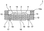
- Front sectional drawing which shows the light-emitting device of embodiment of this invention
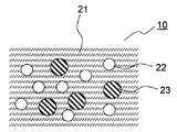
- the conceptual diagram which shows the internal cross section of the package of the light-emitting device of embodiment of this invention.
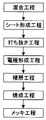
- Process drawing which shows the manufacturing process of the package of the light-emitting device of embodiment of this invention
- FIG. 1 is a perspective view showing a light emitting device according to an embodiment.
- the light-emitting device 1 includes a sintered package 10 whose main component is ceramics 21 (see FIG. 3). As will be described in detail later, the ceramic 21 may or may not contain a glass component.
- a hole 10a for accommodating the light emitting element 2 made of LED is recessed. Light emitted from the light emitting element 2 is reflected by the peripheral wall and the bottom wall of the hole 10a and guided in a predetermined direction.
- the hole 10 a is filled with a sealing material 3 for sealing the light emitting element 2.
- the sealing material 3 is made of a transparent resin containing dispersed phosphor particles for wavelength conversion of light.
- the light emitting element 2 emits blue light, and the phosphor converts the wavelength of the blue light into yellow light.
- FIG. 2 shows a front sectional view of the light emitting device 1.
- the package 10 is formed by laminating a plurality of ceramic sheets 12.
- the ceramic sheet 12 at the top of the package 10 is formed with a through hole that forms a hole 10a.
- the heat dissipation via 18 and the electrode via 19 penetrate the ceramic sheet 12 at the bottom of the package 10.
- the heat radiating via 18 and the electrode via 19 are filled with a conductive material.
- a heat transfer portion 14 is formed on the upper surface of the heat dissipation via 18, and a heat dissipation portion 16 is formed on the lower surface.
- the light emitting element 2 is fixed on the heat transfer section 14 by adhesion or the like and is installed on the bottom surface of the hole 10a.
- the heat generated by the light emitting element 2 is transmitted from the heat transfer section 14 to the heat radiating section 16 through the heat radiating via 18 and radiated.
- a terminal 13 is formed on the upper surface of the electrode via 19, and an electrode 17 is formed on the lower surface.
- the terminal 13 and the electrode 17 are electrically connected by the electrode via 19.
- the light emitting element 2 is connected to the terminal 13 by wire bonding of the wire 4.
- FIG. 3 is a conceptual diagram showing an internal cross section of the package 10.
- the package 10 mainly composed of the ceramic 21 contains particles of the high refractive index material 23 and pores 22.
- the ceramic 21 for example, glass ceramics containing borosilicate glass and alumina, glass ceramics containing soda lime glass and alumina, aluminum nitride, alumina, or the like can be used.
- the high refractive index material 23 is made of a material having a higher refractive index than the ceramic 21.
- the high refractive index material 23 for example, tantalum pentoxide, niobium pentoxide, titanium oxide, barium oxide, barium sulfate, magnesium oxide, calcium oxide, strontium oxide, zinc oxide, zirconium oxide, or the like can be used.
- the pores 22 are formed by burning spacers mixed before firing.
- the diameter of the pores 22 is formed larger than 190 nm.
- FIG. 4 is a process diagram showing the manufacturing process of the package 10.
- a raw material of ceramic 21 (ceramic raw material), a raw material of high refractive index material 23, and a spacer made of granular resin are mixed to generate a mixture.
- the raw material of the ceramic raw material and the high refractive index material 23 is formed of, for example, powder pulverized to a predetermined particle size.
- the spacer is made of a resin, polyethylene, polypropylene, nylon, acrylic, or the like that can be burned in a baking process described later to form pores 22 and burnable at the baking temperature is used.
- the spacer is formed in a size and shape corresponding to the pores 22 having a desired size and shape.
- the spacer is formed in a shape having a sharp portion such as a star shape, cracks may be generated from the pores 22 in the package 10 due to heating or the like during wire bonding when the content rate of the pores 22 is large.
- the spacer is formed in a polyhedron having a spherical shape without a sharp portion or a polygon having an obtuse internal angle.
- the spacer is formed to have a particle size larger than 190 nm, which is a half wavelength of the lower limit wavelength of visible light.
- the pores 22 can be formed with a diameter larger than 190 nm. Therefore, when visible light enters the package 10, the light does not pass through the pores 22, and the light can be reflected at the interfaces of the pores 22.
- the mixture generated in the mixing step is pressurized and formed into a sheet having a thickness of 0.1 mm, for example, to form the material of the ceramic sheet 12.
- the material of the ceramic sheet 12 is punched to form through holes that serve as the hole 10a, the heat dissipation via 18, and the electrode via 19.
- conductors to be terminals 13, electrodes 17, heat transfer portions 14, and heat dissipation portions 16 are formed on the material of the ceramic sheet 12 by printing.
- the materials of the ceramic sheets 12 are temporarily pressed and laminated by low-temperature heating. Thereby, the material of the housing 10 is formed.
- the material of the housing 10 is fired at about 900 ° C. in a firing furnace, and a sintered body of the housing 10 is formed. At this time, since the spacer is made of resin, it burns to form pores 22.
- the terminal 13, the electrode 17, the heat transfer part 14, and the heat dissipation part 16 are plated. Thereby, the housing 10 is obtained.
- the blue light emitted from the light emitting element 2 is guided through the sealing material 3 and is converted into yellow light when reaching the phosphor. Then, the wavelength-converted yellow light and the blue light that does not reach the phosphor are mixed, and white light is emitted from the upper surface of the hole 10a.
- the light guided through the sealing material 3 is reflected by the bottom wall and the peripheral wall of the hole 10a of the housing 10 and is emitted from the upper surface of the hole 10a. Thereby, the light-emitting device 1 emits light in a range corresponding to the size of the hole 10a.
- the package 10 At this time, light incident on the package 10 is reflected at the interface between the particles of the ceramics 21 and the pores 22 due to the difference in refractive index, and is also reflected at the interface between the particles of the ceramics 21 and the particles of the high refractive index material 23. For this reason, by containing the high refractive index material 23 in the package 10, the content of the pores 22 can be reduced and the strength of the package 10 can be improved without reducing the amount of reflected light. Since the refractive index of the medium varies depending on the wavelength, the ceramic 21 and the high refractive index material 23 are selected according to the wavelength of light used.
- the refractive index of the pores 22 is about 1.0.
- the ceramic 21 for example, when glass ceramics mainly composed of zinc borosilicate glass and alumina are used, the refractive index of zinc borosilicate glass is about 1.4, and the refractive index of alumina is about 1.5.
- the high refractive index material 23 the refractive index of zirconium oxide is about 2.0.
- the difference in refractive index between the ceramic 21 and the pores 22 is 0.4 to 0.5, and the difference in refractive index between the ceramic 21 and the high refractive index material 23 is 0.5 to 0.6. For this reason, the same amount of light is reflected at the interface between the pores 22 and the high refractive index material 23.
- the higher refractive index material 23 is desirable because the reflected light increases when the refractive index difference with the ceramic 21 is larger.
- the high refractive index material 23 such as zirconium oxide having a large refractive index difference from the ceramic 21 is very expensive.
- the difference in refractive index with the ceramic 21 is reduced.
- the refractive index is about 1.7, so the difference in refractive index from the ceramic 21 is 0.2 to 0.3.
- the high refractive index material 23 having a small difference in refractive index with the ceramic 21 is included, the amount of reflected light of the package 10 is reduced. For this reason, it is more desirable to form the package 10 so that the total surface area of the pores 22 is larger than the total surface area of the high refractive index material 23.
- the mixing step when the average diameter of the spacer is D1, the volume content is V1, the average diameter of the raw material of the high refractive index material 23 is D2, and the volume content is V2, V1 / D1> V2 / D2.
- the mixture is formed so as to have the following relationship.
- the average diameter of the pores 22 of the sintered body of the housing 10 is D1
- the volume content is V1
- the average diameter of the high refractive index material 23 is D2
- the volume content is V2.
- the sintered body of the housing 10 has a relationship of V1 / D1> V2 / D2, and the total surface area of the pores 22 can be made larger than the total surface area of the high refractive index material 23.
- the strength of the housing 10 can be maintained at an appropriate volume content V1 of the pores 22 and the total surface area of the pores 22 can be increased.
- the glass ceramics are produced, for example, by adding an additive to a borosilicate glass system to produce a glass, then pulverizing it to form a powder, and mixing with a ceramic powder such as alumina.
- the refractive index can be changed by adding barium oxide, zinc oxide, titanium oxide or the like as an additive in the borosilicate glass system.
- the average refractive index of the ceramics 21 made of glass ceramics can be made larger than 1.5, for example.
- the difference in refractive index between the ceramic 21 and the pores 22 can be increased, and the light reflected at the interface of the pores 22 can be increased.
- the difference in refractive index between the ceramic 21 and the high refractive index material 23 is smaller than the difference in refractive index between the ceramic 21 and the pores 22, but the surface area of the pores 22 is larger than the surface area of the high refractive index material 23.
- the luminous efficiency can be improved.
- the package 10 has the pores 22 formed by burning the spacers made by mixing the ceramic raw material and the granular resin and burning the spacers. Therefore, the package 10 having pores having a desired content rate. Can be easily formed. Therefore, the manufacturing cost of the package 10 and the light emitting device 1 can be reduced.
- the spacer is formed in a polyhedron having a spherical shape or a polygon having an obtuse angle, the formation of sharp pores 22 such as a star shape can be prevented, and the strength of the package 10 can be improved.
- the spacer has a particle diameter larger than 190 nm, the pores 22 are formed with a diameter larger than 190 nm. Therefore, visible light incident on the package 10 can be reflected at the interface of the pores 22 without being transmitted.
- the package 10 contains the high refractive index material 23, the content of the pores 22 can be reduced and the strength of the package 10 can be maintained without reducing the amount of reflected light of the package 10.
- the average diameter of the pores 22 is D1
- the volume content is V1
- the average diameter of the high refractive index material 23 is D2
- the volume content is V2, V1 / D1> V2 / D2. Therefore, even if the difference in refractive index between the ceramic 21 and the high refractive index material 23 is small, a decrease in light emission efficiency can be suppressed.
- the difference in refractive index between the ceramic 21 and the pores 22 is larger than the difference in refractive index between the ceramic 21 and the high refractive index material 23, the inexpensive high refractive index material 23 with a small difference in refractive index from the ceramic 21. Can be used.
- the high refractive index material 23 is contained in the package 10, but the high refractive index material 23 may be omitted.
- the present invention can be used for an edge light type backlight, a light source for a scanner, an LED illumination, etc., in which a light emitting device in which a light emitting element is housed in a light emitting device package is mounted.
Landscapes
- Led Device Packages (AREA)
Abstract
【課題】製造コストを削減できる発光装置用パッケージ及びその製造方法を提供する。 【解決手段】セラミックスを主成分とし、発光素子2を収納するとともに発光素子2の出射光を所定方向に反射させる発光装置用パッケージ10の製造方法において、セラミックス原料と粒状の樹脂から成るスペーサとを混合して混合物を生成する混合工程と、該混合物を焼成してスペーサの燃焼により形成される気孔22を有した焼結体を形成する焼成工程とを備えた。
Description
本発明は、パッケージ内に発光素子を収納した発光装置に関する。また本発明は、発光素子を収納する発光装置用パッケージ及びその製造方法に関する。
従来の発光装置は特許文献1に開示されている。この発光装置はアルミナセラミックスやガラスセラミックス等のセラミックスを主成分とする焼結体により形成されたパッケージを備えている。パッケージはセラミックス原料を所定形状に成形した後に焼成され、セラミックス原料の粒子間に生じる隙間によって気孔を有した多孔質に形成される。
パッケージは配線導体を形成した基体と基体上に接着固定される環状の反射部とを有している。反射部の内部にはLED等の発光素子が収納され、発光素子はワイヤーボンディング等により配線導体に接続される。そして、反射部の内部に透明樹脂から成る封止材を充填して発光素子が封止される。
発光素子の発光は封止材を導光し、基体表面及び反射部の内壁で反射して上方に導かれる。これにより、発光装置の上面から所定の範囲に光が出射される。
パッケージは気孔を有するため、封止材が基体及び反射部の表面の気孔内に浸透する。これにより、封止材とパッケージとの固着強度を向上させることができる。また、セラミックスの粒子と気孔との屈折率の差によって両者の界面での反射光量が増加する。これにより、パッケージの反射率が向上して発光装置の発光効率を向上させることができる。
しかしながら、上記従来の発光装置によると、パッケージの気孔が成形時にセラミックス原料の粒子間に生じる隙間によって形成されるため、成形時や焼成時の圧力や温度等の加工条件によって気孔の含有率が変動する。このため、所望の含有率の気孔を有するパッケージを得るために成形時や焼成時の加工条件を高精度に制御する必要がある。従って、パッケージ及び発光装置の製造コストが大きくなる問題があった。
本発明は、製造コストを削減できる発光装置用パッケージ及びその製造方法を提供することを目的とする。また本発明は、製造コストを削減できる発光装置を提供することを目的とする。
上記目的を達成するために本発明は、セラミックスを主成分とし、発光素子を収納するとともに前記発光素子の出射光を所定方向に反射させる発光装置用パッケージの製造方法において、セラミックス原料と粒状の樹脂から成るスペーサとを混合して混合物を生成する混合工程と、前記混合物を焼成して前記スペーサの燃焼により形成される気孔を有した焼結体を形成する焼成工程とを備えたことを特徴としている。
この構成によると、発光装置用パッケージは混合工程でセラミックス原料とスペーサとを混合して混合物が生成される。混合物は所定の形状に成形して焼成工程で焼成され、セラミックスを主成分とした焼結体が形成される。この時、樹脂から成るスペーサが焼成時の加熱によって燃焼して消滅し、セラミックスの粒子間にはスペーサの消滅による気孔が形成される。
また本発明は、上記構成の発光装置用パッケージの製造方法において、前記スペーサが球状または内角が鈍角の多角形による多面体に形成されることを特徴としている。この構成によると、星形等の尖鋭な形状の気孔の形成が防止される。
また本発明は、上記構成の発光装置用パッケージの製造方法において、前記スペーサの粒径が190nmよりも大きいことを特徴としている。この構成によると、気孔の界面で可視光を反射させることができる。
また本発明は、上記構成の発光装置用パッケージの製造方法において、前記混合物が前記セラミックスよりも屈折率の高い高屈折率材の原料を含み、前記焼結体の前記気孔の平均径をD1、体積含有率をV1とし、前記高屈折率材の平均径をD2、体積含有率をV2としたときに、V1/D1>V2/D2の関係を有することを特徴としている。
この構成によると、混合工程で高屈折率材の原料、セラミックス原料及びスペーサを混合して混合物が生成され、焼成工程で焼成して焼結体が形成される。発光装置用パッケージに入射する光はセラミックスの粒子と気孔との界面で反射するとともに、セラミックスの粒子と高屈折率材の粒子との界面で反射する。これにより、発光効率を低下させずに発光装置用パッケージの気孔の含有率を低くして発光装置用パッケージの強度を向上することができる。この時、焼結体内の気孔の表面積が高屈折率材の表面積よりも大きいため、セラミックスと高屈折率材との屈折率の差が小さくても発光効率の低下を抑制することができる。
また本発明は、上記構成の発光装置用パッケージの製造方法において、前記セラミックスと前記気孔との屈折率の差が前記セラミックスと前記高屈折率材との屈折率の差よりも大きいことを特徴としている。この構成によると、セラミックスとの屈折率の差が小さい安価な高屈折率材を用いることができる。
また本発明は、上記構成の発光装置用パッケージの製造方法において、前記セラミックスがガラスを含むガラスセラミックスから成ることを特徴としている。
また本発明は、セラミックスを主成分とし、発光素子を収納するとともに前記発光素子の出射光を所定方向に反射させる発光装置用パッケージにおいて、セラミックス原料と粒状の樹脂から成るスペーサとを混合して焼成し、前記スペーサの燃焼により形成された気孔を有することを特徴としている。
また本発明は、上記構成の発光装置用パッケージにおいて、前記スペーサが球状または内角が鈍角の多角形による多面体に形成されることを特徴としている。
また本発明は、上記構成の発光装置用パッケージにおいて、前記スペーサの粒径が190nmよりも大きいことを特徴としている。
また本発明は、上記構成の発光装置用パッケージにおいて、前記セラミックスよりも屈折率の高い高屈折率材を含み、前記気孔の平均径をD1、体積含有率をV1とし、前記高屈折率材の平均径をD2、体積含有率をV2としたときに、V1/D1>V2/D2の関係を有することを特徴としている。
また本発明は、上記構成の発光装置用パッケージにおいて、前記セラミックスと前記気孔との屈折率の差が前記セラミックスと前記高屈折率材との屈折率の差よりも大きいことを特徴としている。
また本発明は、上記構成の発光装置用パッケージにおいて、前記セラミックスがガラスを含むガラスセラミックスから成ることを特徴としている。
また本発明の発光装置は、上記各構成の発光装置用パッケージ内に発光素子を収納したことを特徴としている。
本発明によると、発光装置用パッケージがセラミックス原料と粒状の樹脂から成るスペーサとを混合して焼成し、スペーサの燃焼により形成された気孔を有するので、所望の含有率の気孔を有した発光装置用パッケージを容易に形成することができる。従って、発光装置用パッケージ及び発光装置の製造コストを削減することができる。
以下に本発明の実施形態を図面を参照して説明する。図1は一実施形態の発光装置を示す斜視図ある。発光装置1はセラミックス21(図3参照)を主成分とした焼結体のパッケージ10を備えている。詳細を後述するように、セラミックス21はガラス成分を含んでもよく、含まなくてもよい。パッケージ10の上面にはLEDから成る発光素子2を収納する孔部10aが凹設される。発光素子2の発光は孔部10aの周壁及び底壁で反射して所定方向に導かれる。
孔部10aには発光素子2を封止する封止材3が充填される。封止材3は光を波長変換する蛍光体の粒子を分散して含有した透明樹脂から成る。本実施形態では発光素子2は青色光を発光し、蛍光体は青色光を黄色光に波長変換する。
図2は発光装置1の正面断面図を示している。パッケージ10は複数のセラミックシート12を積層して形成される。パッケージ10の上部のセラミックシート12には孔部10aを形成する貫通孔が形成される。パッケージ10の下部のセラミックシート12には放熱ビア18及び電極ビア19が貫通する。放熱ビア18及び電極ビア19には導電性材料が充填される。放熱ビア18の上面には伝熱部14が形成され、下面には放熱部16が形成される。
発光素子2は接着等により伝熱部14上に固着して孔部10aの底面に設置される。発光素子2の発熱は伝熱部14から放熱ビア18を介して放熱部16に伝えられて放熱する。電極ビア19の上面には端子13が形成され、下面には電極17が形成される。電極ビア19によって端子13と電極17とが導通する。発光素子2はワイヤー4をワイヤーボンディングして端子13に接続される。
図3はパッケージ10の内部断面を示す概念図である。セラミックス21を主成分とするパッケージ10内には高屈折率材23の粒子及び気孔22が含有される。セラミックス21として、例えば、ホウ珪酸ガラス及びアルミナを含むガラスセラミックス、ソーダ石灰ガラス及びアルミナを含むガラスセラミックス、窒化アルミニウム、アルミナ等を用いることができる。
高屈折率材23はセラミックス21よりも屈折率の高い材料により形成される。高屈折率材23として、例えば、五酸化タンタル、五酸化ニオブ、酸化チタン、酸化バリウム、硫酸バリウム、酸化マグネシウム、酸化カルシウム、酸化ストロンチウム、酸化亜鉛、酸化ジルコニウム等を用いることができる。
気孔22は後述するように焼成前に混合されるスペーサの燃焼によって形成される。気孔22の径は190nmよりも大きく形成される。
図4はパッケージ10の製造工程を示す工程図である。混合工程ではセラミックス21の原料(セラミックス原料)、高屈折率材23の原料、及び粒状の樹脂から成るスペーサとを混合して混合物を生成する。セラミックス原料及び高屈折率材23の原料は例えば、所定の粒径に粉砕された粉体により形成される。
スペーサは樹脂から成るため後述する焼成工程で燃焼して気孔22を形成し、焼成温度で燃焼可能なポリエチレン、ポリプロピレン、ナイロン、アクリル等が用いられる。スペーサは所望の大きさや形状の気孔22に応じた大きさや形状に形成される。この時、スペーサを星形等の尖鋭部分を有する形状に形成すると、気孔22の含有率が多いときにワイヤーボンディング時の加熱等によってパッケージ10に気孔22からヒビが発生する場合がある。このため、スペーサは尖鋭部分を持たない球状や内角が鈍角の多角形による多面体等に形成される。
また、スペーサは可視光の下限波長の半波長である190nmよりも大きい粒径に形成される。これにより、気孔22を190nmよりも大きい径に形成することができる。従って、パッケージ10に可視光が入射した際に光が気孔22を透過せず、気孔22の界面で光を反射させることができる。
シート形成工程では混合工程で生成した混合物を加圧して例えば、厚さ0.1mmのシート状に成形し、セラミックシート12の素材を形成する。打ち抜き工程ではセラミックシート12の素材を打ち抜き、孔部10a、放熱ビア18及び電極ビア19となる貫通孔を形成する。電極形成工程では印刷によってセラミックシート12の素材上に端子13、電極17、伝熱部14及び放熱部16となる導体を形成する。
積層工程では各セラミックシート12の素材が低温加熱により仮圧着して積層される。これにより、ハウジング10の素材が形成される。焼成工程ではハウジング10の素材が焼成炉により約900℃で焼成され、ハウジング10の焼結体が形成される。この時、スペーサが樹脂から成るため燃焼して気孔22が形成される。
メッキ工程では端子13、電極17、伝熱部14及び放熱部16にメッキが施される。これにより、ハウジング10が得られる。
上記構成の発光装置1において、発光素子2により発光した青色光は封止材3を導光し、蛍光体に到達すると黄色光に波長変換される。そして、波長変換された黄色光と蛍光体に到達しない青色光とが混合して白色光が孔部10aの上面から出射される。また、封止材3を導光した光はハウジング10の孔部10aの底壁及び周壁で反射して孔部10aの上面から出射される。これにより、発光装置1は孔部10aの大きさに応じた範囲に光を出射する。
この時、パッケージ10に入射する光は屈折率の差によってセラミックス21の粒子と気孔22との界面で反射するとともに、セラミックス21の粒子と高屈折率材23の粒子との界面で反射する。このため、パッケージ10に高屈折率材23を含有することにより、反射光量を低下させずに気孔22の含有量を減らしてパッケージ10の強度を向上させることができる。尚、媒質の屈折率は波長によって変動するため、使用される光の波長に応じてセラミックス21及び高屈折率材23が選定される。
気孔22の屈折率は約1.0である。セラミックス21の一例として例えば、ホウ珪酸亜鉛ガラスとアルミナとを主成分とするガラスセラミックスを用いると、ホウ珪酸亜鉛ガラスの屈折率は約1.4、アルミナの屈折率は約1.5である。また、高屈折率材23の一例として酸化ジルコニウムの屈折率は約2.0である。この時、セラミックス21と気孔22との屈折率の差は0.4~0.5であり、セラミックス21と高屈折率材23との屈折率の差は0.5~0.6である。このため、気孔22及び高屈折率材23の界面で同程度の量の光が反射する。
高屈折率材23はセラミックス21との屈折率の差が大きい方が反射する光が増加するため望ましい。しかしながら、セラミックス21との屈折率の差が大きい酸化ジルコニウム等の高屈折率材23は非常に高価である。
このため、安価な高屈折率材23を用いると、セラミックス21との屈折率の差が小さくなる。例えば、高屈折率材23として酸化マグネシウムを用いると、屈折率が約1.7であるためセラミックス21との屈折率の差が0.2~0.3となる。この時、セラミックス21との屈折率の差が小さい高屈折率材23が多く含まれるとパッケージ10の反射光量が少なくなる。このため、気孔22の総表面積が高屈折率材23の総表面積よりも大きくなるようにパッケージ10を形成するとより望ましい。
即ち、混合工程において、スペーサの平均径をD1、体積含有率をV1とし、高屈折率材23の原料の平均径をD2、体積含有率をV2としたときに、V1/D1>V2/D2の関係を有するように混合物を生成する。これにより、ハウジング10の焼結体の気孔22の平均径がD1、体積含有率がV1となり、高屈折率材23の平均径がD2、体積含有率がV2となる。この時、ハウジング10の焼結体はV1/D1>V2/D2の関係を有し、気孔22の総表面積を高屈折率材23の総表面積よりも大きくすることができる。また、スペーサの平均径D1を小さくすることで、適正な気孔22の体積含有率V1でハウジング10の強度を維持して気孔22の総表面積を増加させることができる。
尚、ガラスセラミックスは例えば、ホウ珪酸ガラス系に添加物を添加してガラスを作製した後粉砕して粉体に形成し、アルミナ等のセラミックスの粉体と混合して作製される。ホウ珪酸ガラス系の中で添加物として酸化バリウム、酸化亜鉛、酸化チタン等を添加することによって屈折率を変更することができる。
これにより、ガラスセラミックスから成るセラミックス21の平均の屈折率を例えば、1.5よりも大きくすることができる。その結果、セラミックス21と気孔22との屈折率の差を大きくすることができ、気孔22の界面で反射する光を増加させることができる。この時、セラミックス21と気孔22との屈折率の差よりもセラミックス21と高屈折率材23との屈折率の差が小さくなるが、気孔22の表面積を高屈折率材23の表面積よりも大きくして発光効率を向上させることができる。
本実施形態によると、パッケージ10がセラミックス原料と粒状の樹脂から成るスペーサとを混合して焼成し、スペーサの燃焼により形成された気孔22を有するので、所望の含有率の気孔を有したパッケージ10を容易に形成することができる。従って、パッケージ10及び発光装置1の製造コストを削減することができる。
また、スペーサが球状または内角が鈍角の多角形による多面体に形成されるので、星形等の尖鋭な形状の気孔22の形成を防止し、パッケージ10の強度を向上することができる。
また、スペーサの粒径が190nmよりも大きいので、気孔22が190nmよりも大きい径に形成される。従って、パッケージ10に入射した可視光を透過させずに気孔22の界面で反射させることができる。
また、パッケージ10が高屈折率材23を含有するので、パッケージ10の反射光量を低下させずに気孔22の含有量を減らしてパッケージ10の強度を維持することができる。この時、気孔22の平均径をD1、体積含有率をV1とし、高屈折率材23の平均径をD2、体積含有率をV2としたときに、V1/D1>V2/D2の関係を有するので、セラミックス21と高屈折率材23との屈折率の差が小さくても発光効率の低下を抑制することができる。
また、セラミックス21と気孔22との屈折率の差がセラミックス21と高屈折率材23との屈折率の差よりも大きいので、セラミックス21との屈折率の差が小さい安価な高屈折率材23を用いることができる。
本実施形態において、パッケージ10内に高屈折率材23を含有しているが、高屈折率材23を省いてもよい。
本発明によると、発光装置用パッケージ内に発光素子を収納した発光装置を搭載するエッジライト型バックライト、スキャナ用光源、LED照明等に利用することができる。
1 発光装置
2 発光素子
3 封止材
4 ワイヤー
10 パッケージ
10a 孔部
12 セラミックシート
13 端子
14 伝熱部
16 放熱部
17 電極
18 放熱ビア
19 電極ビア
21 セラミックス
22 気孔
23 高屈折率材
2 発光素子
3 封止材
4 ワイヤー
10 パッケージ
10a 孔部
12 セラミックシート
13 端子
14 伝熱部
16 放熱部
17 電極
18 放熱ビア
19 電極ビア
21 セラミックス
22 気孔
23 高屈折率材
Claims (13)
- セラミックスを主成分とし、発光素子を収納するとともに前記発光素子の出射光を所定方向に反射させる発光装置用パッケージの製造方法において、セラミックス原料と粒状の樹脂から成るスペーサとを混合して混合物を生成する混合工程と、前記混合物を焼成して前記スペーサの燃焼により形成される気孔を有した焼結体を形成する焼成工程とを備えたことを特徴とする発光装置用パッケージの製造方法。
- 前記スペーサは球状または内角が鈍角の多角形による多面体に形成されることを特徴とする請求項1に記載の発光装置用パッケージの製造方法。
- 前記スペーサの粒径が190nmよりも大きいことを特徴とする請求項1に記載の発光装置用パッケージの製造方法。
- 前記混合物が前記セラミックスよりも屈折率の高い高屈折率材の原料を含み、前記焼結体の前記気孔の平均径をD1、体積含有率をV1とし、前記高屈折率材の平均径をD2、体積含有率をV2としたときに、V1/D1>V2/D2の関係を有することを特徴とする請求項1に記載の発光装置用パッケージの製造方法。
- 前記セラミックスと前記気孔との屈折率の差が前記セラミックスと前記高屈折率材との屈折率の差よりも大きいことを特徴とする請求項4に記載の発光装置用パッケージの製造方法。
- 前記セラミックスがガラスを含むガラスセラミックスから成ることを特徴とする請求項1に記載の発光装置用パッケージの製造方法。
- セラミックスを主成分とし、発光素子を収納するとともに前記発光素子の出射光を所定方向に反射させる発光装置用パッケージにおいて、セラミックス原料と粒状の樹脂から成るスペーサとを混合して焼成し、前記スペーサの燃焼により形成された気孔を有することを特徴とする発光装置用パッケージ。
- 前記スペーサが球状または内角が鈍角の多角形による多面体に形成されることを特徴とする請求項7に記載の発光装置用パッケージ。
- 前記スペーサの粒径が190nmよりも大きいことを特徴とする請求項7に記載の発光装置用パッケージ。
- 前記セラミックスよりも屈折率の高い高屈折率材を含み、前記気孔の平均径をD1、体積含有率をV1とし、前記高屈折率材の平均径をD2、体積含有率をV2としたときに、V1/D1>V2/D2の関係を有することを特徴とする請求項7に記載の発光装置用パッケージ。
- 前記セラミックスと前記気孔との屈折率の差が前記セラミックスと前記高屈折率材との屈折率の差よりも大きいことを特徴とする請求項10に記載の発光装置用パッケージ。
- 前記セラミックスがガラスを含むガラスセラミックスから成ることを特徴とする請求項7に記載の発光装置用パッケージ。
- 請求項7に記載の発光装置用パッケージ内に発光素子を収納したことを特徴とする発光装置。
Applications Claiming Priority (2)
| Application Number | Priority Date | Filing Date | Title |
|---|---|---|---|
| JP2010-193809 | 2010-08-31 | ||
| JP2010193809A JP2013232443A (ja) | 2010-08-31 | 2010-08-31 | 発光装置、発光装置用パッケージ及び発光装置用パッケージの製造方法 |
Publications (1)
| Publication Number | Publication Date |
|---|---|
| WO2012029684A1 true WO2012029684A1 (ja) | 2012-03-08 |
Family
ID=45772772
Family Applications (1)
| Application Number | Title | Priority Date | Filing Date |
|---|---|---|---|
| PCT/JP2011/069381 Ceased WO2012029684A1 (ja) | 2010-08-31 | 2011-08-29 | 発光装置、発光装置用パッケージ及び発光装置用パッケージの製造方法 |
Country Status (2)
| Country | Link |
|---|---|
| JP (1) | JP2013232443A (ja) |
| WO (1) | WO2012029684A1 (ja) |
Cited By (1)
| Publication number | Priority date | Publication date | Assignee | Title |
|---|---|---|---|---|
| JP2015149417A (ja) * | 2014-02-07 | 2015-08-20 | 日本特殊陶業株式会社 | 発光素子搭載用セラミックパッケージ |
Citations (3)
| Publication number | Priority date | Publication date | Assignee | Title |
|---|---|---|---|---|
| JP2005255747A (ja) * | 2004-03-10 | 2005-09-22 | Fine Rubber Kenkyusho:Kk | 蛍光部材及び半導体発光装置 |
| JP2007227868A (ja) * | 2006-01-30 | 2007-09-06 | Kyocera Corp | 発光装置および照明装置 |
| JP2009162950A (ja) * | 2007-12-28 | 2009-07-23 | Sumitomo Metal Electronics Devices Inc | 反射材およびそれを用いた反射体 |
-
2010
- 2010-08-31 JP JP2010193809A patent/JP2013232443A/ja active Pending
-
2011
- 2011-08-29 WO PCT/JP2011/069381 patent/WO2012029684A1/ja not_active Ceased
Patent Citations (3)
| Publication number | Priority date | Publication date | Assignee | Title |
|---|---|---|---|---|
| JP2005255747A (ja) * | 2004-03-10 | 2005-09-22 | Fine Rubber Kenkyusho:Kk | 蛍光部材及び半導体発光装置 |
| JP2007227868A (ja) * | 2006-01-30 | 2007-09-06 | Kyocera Corp | 発光装置および照明装置 |
| JP2009162950A (ja) * | 2007-12-28 | 2009-07-23 | Sumitomo Metal Electronics Devices Inc | 反射材およびそれを用いた反射体 |
Cited By (1)
| Publication number | Priority date | Publication date | Assignee | Title |
|---|---|---|---|---|
| JP2015149417A (ja) * | 2014-02-07 | 2015-08-20 | 日本特殊陶業株式会社 | 発光素子搭載用セラミックパッケージ |
Also Published As
| Publication number | Publication date |
|---|---|
| JP2013232443A (ja) | 2013-11-14 |
Similar Documents
| Publication | Publication Date | Title |
|---|---|---|
| US9599292B2 (en) | Light emitting module, a lamp, a luminaire and a display device | |
| US9082946B2 (en) | Light emitting module, a lamp, a luminaire and a display device | |
| JP5393796B2 (ja) | 発光装置 | |
| JP2012195404A (ja) | 発光装置および照明装置 | |
| JP4926481B2 (ja) | 発光ダイオード用パッケージ及び発光ダイオード | |
| US20160064624A1 (en) | Semiconductor light emitting device and light emitting device package | |
| JP2013251285A (ja) | 発光装置用パッケージ及びその製造方法 | |
| US10964859B2 (en) | Light-emitting device and method of manufacturing the same | |
| JP2018107418A (ja) | 発光装置 | |
| JP2013232443A (ja) | 発光装置、発光装置用パッケージ及び発光装置用パッケージの製造方法 | |
| US20190237639A1 (en) | Light-emitting device and method of manufacturing the same | |
| JP2012227454A (ja) | 発光装置用パッケージ及びそれを用いた発光装置 | |
| JP2012226227A (ja) | 反射材及びそれを用いた発光装置用パッケージ | |
| JP2012204767A (ja) | 発光装置用パッケージ及び発光装置 | |
| JP2012204766A (ja) | 発光装置用パッケージ及び発光装置 | |
| WO2019150739A1 (ja) | 発光装置及びその製造方法 | |
| JP2008117932A (ja) | リフレクターとそれを備えた発光素子収納用パッケージと発光装置 | |
| JPWO2012105092A1 (ja) | 発光装置用パッケージ | |
| CN222814799U (zh) | 一种芯片级led封装元件 | |
| JP2015162505A (ja) | 発光素子搭載用基板およびそれを用いた発光装置 | |
| CN102637807A (zh) | 一种改进的白光led器件 | |
| JP2009004434A (ja) | セラミックス焼結体およびそれを用いた反射体およびそれを用いた発光素子搭載用パッケージおよびそれを用いた発光装置 | |
| JP6266369B2 (ja) | 発光素子搭載用セラミックパッケージ | |
| KR20140015958A (ko) | 발광 소자 패키지 | |
| JP2012227224A (ja) | 発光装置 |
Legal Events
| Date | Code | Title | Description |
|---|---|---|---|
| 121 | Ep: the epo has been informed by wipo that ep was designated in this application |
Ref document number: 11821700 Country of ref document: EP Kind code of ref document: A1 |
|
| NENP | Non-entry into the national phase |
Ref country code: DE |
|
| 122 | Ep: pct application non-entry in european phase |
Ref document number: 11821700 Country of ref document: EP Kind code of ref document: A1 |
|
| NENP | Non-entry into the national phase |
Ref country code: JP |