WO2012023558A1 - 発光ダイオード及び発光ダイオードランプ - Google Patents
発光ダイオード及び発光ダイオードランプ Download PDFInfo
- Publication number
- WO2012023558A1 WO2012023558A1 PCT/JP2011/068563 JP2011068563W WO2012023558A1 WO 2012023558 A1 WO2012023558 A1 WO 2012023558A1 JP 2011068563 W JP2011068563 W JP 2011068563W WO 2012023558 A1 WO2012023558 A1 WO 2012023558A1
- Authority
- WO
- WIPO (PCT)
- Prior art keywords
- light
- layer
- light emitting
- emitting diode
- substrate
- Prior art date
Links
- 239000000758 substrate Substances 0.000 claims abstract description 257
- 239000004065 semiconductor Substances 0.000 claims abstract description 109
- 150000001875 compounds Chemical class 0.000 claims abstract description 89
- 238000000605 extraction Methods 0.000 claims abstract description 86
- 230000004888 barrier function Effects 0.000 claims abstract description 38
- 230000004044 response Effects 0.000 claims abstract description 29
- 229910052751 metal Inorganic materials 0.000 claims description 113
- 239000002184 metal Substances 0.000 claims description 113
- 239000000463 material Substances 0.000 claims description 50
- 239000000203 mixture Substances 0.000 claims description 39
- 238000005253 cladding Methods 0.000 claims description 27
- 238000000295 emission spectrum Methods 0.000 claims description 13
- 230000008635 plant growth Effects 0.000 claims description 12
- 230000029553 photosynthesis Effects 0.000 claims description 8
- 238000010672 photosynthesis Methods 0.000 claims description 8
- 229910052710 silicon Inorganic materials 0.000 claims description 8
- 230000001737 promoting effect Effects 0.000 claims description 3
- 239000000126 substance Substances 0.000 abstract 1
- 239000010410 layer Substances 0.000 description 589
- 239000010408 film Substances 0.000 description 66
- JBRZTFJDHDCESZ-UHFFFAOYSA-N AsGa Chemical compound [As]#[Ga] JBRZTFJDHDCESZ-UHFFFAOYSA-N 0.000 description 43
- 229910001218 Gallium arsenide Inorganic materials 0.000 description 41
- 230000017525 heat dissipation Effects 0.000 description 34
- 230000000694 effects Effects 0.000 description 30
- 230000007547 defect Effects 0.000 description 29
- 238000000034 method Methods 0.000 description 28
- 239000010949 copper Substances 0.000 description 26
- 239000010931 gold Substances 0.000 description 26
- 238000004519 manufacturing process Methods 0.000 description 21
- 230000012010 growth Effects 0.000 description 14
- 239000002356 single layer Substances 0.000 description 13
- 230000007423 decrease Effects 0.000 description 11
- PXHVJJICTQNCMI-UHFFFAOYSA-N Nickel Chemical compound [Ni] PXHVJJICTQNCMI-UHFFFAOYSA-N 0.000 description 10
- 239000000470 constituent Substances 0.000 description 10
- 239000013078 crystal Substances 0.000 description 10
- 238000007689 inspection Methods 0.000 description 10
- 230000005496 eutectics Effects 0.000 description 9
- BASFCYQUMIYNBI-UHFFFAOYSA-N platinum Substances [Pt] BASFCYQUMIYNBI-UHFFFAOYSA-N 0.000 description 9
- PCHJSUWPFVWCPO-UHFFFAOYSA-N gold Chemical compound [Au] PCHJSUWPFVWCPO-UHFFFAOYSA-N 0.000 description 8
- 229910045601 alloy Inorganic materials 0.000 description 7
- 239000000956 alloy Substances 0.000 description 7
- 229910052737 gold Inorganic materials 0.000 description 6
- 238000005286 illumination Methods 0.000 description 6
- 230000008569 process Effects 0.000 description 6
- 238000010586 diagram Methods 0.000 description 5
- 238000005530 etching Methods 0.000 description 5
- 238000010438 heat treatment Methods 0.000 description 5
- 239000011777 magnesium Substances 0.000 description 5
- WFKWXMTUELFFGS-UHFFFAOYSA-N tungsten Chemical compound [W] WFKWXMTUELFFGS-UHFFFAOYSA-N 0.000 description 5
- 229910052721 tungsten Inorganic materials 0.000 description 5
- 239000010937 tungsten Substances 0.000 description 5
- QGZKDVFQNNGYKY-UHFFFAOYSA-N Ammonia Chemical compound N QGZKDVFQNNGYKY-UHFFFAOYSA-N 0.000 description 4
- BQCADISMDOOEFD-UHFFFAOYSA-N Silver Chemical compound [Ag] BQCADISMDOOEFD-UHFFFAOYSA-N 0.000 description 4
- 238000006243 chemical reaction Methods 0.000 description 4
- 229910052802 copper Inorganic materials 0.000 description 4
- 238000005336 cracking Methods 0.000 description 4
- 238000010030 laminating Methods 0.000 description 4
- 229910052759 nickel Inorganic materials 0.000 description 4
- 230000005855 radiation Effects 0.000 description 4
- 230000009467 reduction Effects 0.000 description 4
- 229910052709 silver Inorganic materials 0.000 description 4
- 239000004332 silver Substances 0.000 description 4
- 239000010936 titanium Substances 0.000 description 4
- 229910000980 Aluminium gallium arsenide Inorganic materials 0.000 description 3
- VYZAMTAEIAYCRO-UHFFFAOYSA-N Chromium Chemical compound [Cr] VYZAMTAEIAYCRO-UHFFFAOYSA-N 0.000 description 3
- RYGMFSIKBFXOCR-UHFFFAOYSA-N Copper Chemical compound [Cu] RYGMFSIKBFXOCR-UHFFFAOYSA-N 0.000 description 3
- 229910052782 aluminium Inorganic materials 0.000 description 3
- XAGFODPZIPBFFR-UHFFFAOYSA-N aluminium Chemical compound [Al] XAGFODPZIPBFFR-UHFFFAOYSA-N 0.000 description 3
- 229910052804 chromium Inorganic materials 0.000 description 3
- 239000011651 chromium Substances 0.000 description 3
- 230000001276 controlling effect Effects 0.000 description 3
- 238000009826 distribution Methods 0.000 description 3
- 238000005304 joining Methods 0.000 description 3
- 230000008018 melting Effects 0.000 description 3
- 238000002844 melting Methods 0.000 description 3
- 238000000059 patterning Methods 0.000 description 3
- 238000000206 photolithography Methods 0.000 description 3
- 239000002994 raw material Substances 0.000 description 3
- 230000035882 stress Effects 0.000 description 3
- 238000001771 vacuum deposition Methods 0.000 description 3
- 229910001316 Ag alloy Inorganic materials 0.000 description 2
- ZOKXTWBITQBERF-UHFFFAOYSA-N Molybdenum Chemical compound [Mo] ZOKXTWBITQBERF-UHFFFAOYSA-N 0.000 description 2
- 229910000990 Ni alloy Inorganic materials 0.000 description 2
- XYFCBTPGUUZFHI-UHFFFAOYSA-N Phosphine Chemical compound P XYFCBTPGUUZFHI-UHFFFAOYSA-N 0.000 description 2
- RTAQQCXQSZGOHL-UHFFFAOYSA-N Titanium Chemical compound [Ti] RTAQQCXQSZGOHL-UHFFFAOYSA-N 0.000 description 2
- 239000000853 adhesive Substances 0.000 description 2
- 230000001070 adhesive effect Effects 0.000 description 2
- 229910021529 ammonia Inorganic materials 0.000 description 2
- RBFQJDQYXXHULB-UHFFFAOYSA-N arsane Chemical compound [AsH3] RBFQJDQYXXHULB-UHFFFAOYSA-N 0.000 description 2
- 230000015572 biosynthetic process Effects 0.000 description 2
- 238000005229 chemical vapour deposition Methods 0.000 description 2
- 238000005520 cutting process Methods 0.000 description 2
- 230000006837 decompression Effects 0.000 description 2
- 238000009792 diffusion process Methods 0.000 description 2
- PZPGRFITIJYNEJ-UHFFFAOYSA-N disilane Chemical compound [SiH3][SiH3] PZPGRFITIJYNEJ-UHFFFAOYSA-N 0.000 description 2
- QBJCZLXULXFYCK-UHFFFAOYSA-N magnesium;cyclopenta-1,3-diene Chemical compound [Mg+2].C1C=CC=[C-]1.C1C=CC=[C-]1 QBJCZLXULXFYCK-UHFFFAOYSA-N 0.000 description 2
- 150000002739 metals Chemical class 0.000 description 2
- 229910052750 molybdenum Inorganic materials 0.000 description 2
- 239000011733 molybdenum Substances 0.000 description 2
- 238000001579 optical reflectometry Methods 0.000 description 2
- 230000000243 photosynthetic effect Effects 0.000 description 2
- 229910052697 platinum Inorganic materials 0.000 description 2
- 238000011160 research Methods 0.000 description 2
- 229920005989 resin Polymers 0.000 description 2
- 239000011347 resin Substances 0.000 description 2
- 238000007789 sealing Methods 0.000 description 2
- 230000003746 surface roughness Effects 0.000 description 2
- 239000010409 thin film Substances 0.000 description 2
- 229910052719 titanium Inorganic materials 0.000 description 2
- 239000012780 transparent material Substances 0.000 description 2
- JLTRXTDYQLMHGR-UHFFFAOYSA-N trimethylaluminium Chemical compound C[Al](C)C JLTRXTDYQLMHGR-UHFFFAOYSA-N 0.000 description 2
- XCZXGTMEAKBVPV-UHFFFAOYSA-N trimethylgallium Chemical compound C[Ga](C)C XCZXGTMEAKBVPV-UHFFFAOYSA-N 0.000 description 2
- IBEFSUTVZWZJEL-UHFFFAOYSA-N trimethylindium Chemical compound C[In](C)C IBEFSUTVZWZJEL-UHFFFAOYSA-N 0.000 description 2
- IHGSAQHSAGRWNI-UHFFFAOYSA-N 1-(4-bromophenyl)-2,2,2-trifluoroethanone Chemical compound FC(F)(F)C(=O)C1=CC=C(Br)C=C1 IHGSAQHSAGRWNI-UHFFFAOYSA-N 0.000 description 1
- GYHNNYVSQQEPJS-UHFFFAOYSA-N Gallium Chemical compound [Ga] GYHNNYVSQQEPJS-UHFFFAOYSA-N 0.000 description 1
- 206010037660 Pyrexia Diseases 0.000 description 1
- VYPSYNLAJGMNEJ-UHFFFAOYSA-N Silicium dioxide Chemical compound O=[Si]=O VYPSYNLAJGMNEJ-UHFFFAOYSA-N 0.000 description 1
- GWEVSGVZZGPLCZ-UHFFFAOYSA-N Titan oxide Chemical compound O=[Ti]=O GWEVSGVZZGPLCZ-UHFFFAOYSA-N 0.000 description 1
- HCHKCACWOHOZIP-UHFFFAOYSA-N Zinc Chemical compound [Zn] HCHKCACWOHOZIP-UHFFFAOYSA-N 0.000 description 1
- 230000005856 abnormality Effects 0.000 description 1
- 230000002411 adverse Effects 0.000 description 1
- PNEYBMLMFCGWSK-UHFFFAOYSA-N aluminium oxide Inorganic materials [O-2].[O-2].[O-2].[Al+3].[Al+3] PNEYBMLMFCGWSK-UHFFFAOYSA-N 0.000 description 1
- 238000013459 approach Methods 0.000 description 1
- 230000008901 benefit Effects 0.000 description 1
- 230000000903 blocking effect Effects 0.000 description 1
- 238000004140 cleaning Methods 0.000 description 1
- 238000011109 contamination Methods 0.000 description 1
- 238000012364 cultivation method Methods 0.000 description 1
- 230000006866 deterioration Effects 0.000 description 1
- 238000005516 engineering process Methods 0.000 description 1
- 239000003822 epoxy resin Substances 0.000 description 1
- 238000011156 evaluation Methods 0.000 description 1
- 230000002349 favourable effect Effects 0.000 description 1
- 229910052733 gallium Inorganic materials 0.000 description 1
- 230000020169 heat generation Effects 0.000 description 1
- 230000008642 heat stress Effects 0.000 description 1
- 125000005842 heteroatom Chemical group 0.000 description 1
- 238000007731 hot pressing Methods 0.000 description 1
- 239000012535 impurity Substances 0.000 description 1
- 229910052738 indium Inorganic materials 0.000 description 1
- APFVFJFRJDLVQX-UHFFFAOYSA-N indium atom Chemical compound [In] APFVFJFRJDLVQX-UHFFFAOYSA-N 0.000 description 1
- 230000007246 mechanism Effects 0.000 description 1
- 238000001451 molecular beam epitaxy Methods 0.000 description 1
- 230000003287 optical effect Effects 0.000 description 1
- 230000003647 oxidation Effects 0.000 description 1
- 238000007254 oxidation reaction Methods 0.000 description 1
- 238000005192 partition Methods 0.000 description 1
- 229920000647 polyepoxide Polymers 0.000 description 1
- 238000012545 processing Methods 0.000 description 1
- 238000013139 quantization Methods 0.000 description 1
- 230000035484 reaction time Effects 0.000 description 1
- 230000006798 recombination Effects 0.000 description 1
- 238000005215 recombination Methods 0.000 description 1
- 230000001105 regulatory effect Effects 0.000 description 1
- 230000002040 relaxant effect Effects 0.000 description 1
- 238000007788 roughening Methods 0.000 description 1
- 230000008054 signal transmission Effects 0.000 description 1
- 239000010703 silicon Substances 0.000 description 1
- 229910052814 silicon oxide Inorganic materials 0.000 description 1
- OGIDPMRJRNCKJF-UHFFFAOYSA-N titanium oxide Inorganic materials [Ti]=O OGIDPMRJRNCKJF-UHFFFAOYSA-N 0.000 description 1
- 238000002834 transmittance Methods 0.000 description 1
- 238000007740 vapor deposition Methods 0.000 description 1
- 229910052725 zinc Inorganic materials 0.000 description 1
- 239000011701 zinc Substances 0.000 description 1
Images


Classifications
-
- H—ELECTRICITY
- H10—SEMICONDUCTOR DEVICES; ELECTRIC SOLID-STATE DEVICES NOT OTHERWISE PROVIDED FOR
- H10H—INORGANIC LIGHT-EMITTING SEMICONDUCTOR DEVICES HAVING POTENTIAL BARRIERS
- H10H20/00—Individual inorganic light-emitting semiconductor devices having potential barriers, e.g. light-emitting diodes [LED]
- H10H20/80—Constructional details
- H10H20/81—Bodies
- H10H20/811—Bodies having quantum effect structures or superlattices, e.g. tunnel junctions
-
- H—ELECTRICITY
- H10—SEMICONDUCTOR DEVICES; ELECTRIC SOLID-STATE DEVICES NOT OTHERWISE PROVIDED FOR
- H10H—INORGANIC LIGHT-EMITTING SEMICONDUCTOR DEVICES HAVING POTENTIAL BARRIERS
- H10H20/00—Individual inorganic light-emitting semiconductor devices having potential barriers, e.g. light-emitting diodes [LED]
- H10H20/80—Constructional details
- H10H20/85—Packages
- H10H20/855—Optical field-shaping means, e.g. lenses
- H10H20/856—Reflecting means
-
- H—ELECTRICITY
- H10—SEMICONDUCTOR DEVICES; ELECTRIC SOLID-STATE DEVICES NOT OTHERWISE PROVIDED FOR
- H10H—INORGANIC LIGHT-EMITTING SEMICONDUCTOR DEVICES HAVING POTENTIAL BARRIERS
- H10H20/00—Individual inorganic light-emitting semiconductor devices having potential barriers, e.g. light-emitting diodes [LED]
- H10H20/80—Constructional details
- H10H20/81—Bodies
- H10H20/815—Bodies having stress relaxation structures, e.g. buffer layers
-
- H—ELECTRICITY
- H10—SEMICONDUCTOR DEVICES; ELECTRIC SOLID-STATE DEVICES NOT OTHERWISE PROVIDED FOR
- H10H—INORGANIC LIGHT-EMITTING SEMICONDUCTOR DEVICES HAVING POTENTIAL BARRIERS
- H10H20/00—Individual inorganic light-emitting semiconductor devices having potential barriers, e.g. light-emitting diodes [LED]
- H10H20/80—Constructional details
- H10H20/81—Bodies
- H10H20/822—Materials of the light-emitting regions
- H10H20/824—Materials of the light-emitting regions comprising only Group III-V materials, e.g. GaP
-
- H—ELECTRICITY
- H10—SEMICONDUCTOR DEVICES; ELECTRIC SOLID-STATE DEVICES NOT OTHERWISE PROVIDED FOR
- H10H—INORGANIC LIGHT-EMITTING SEMICONDUCTOR DEVICES HAVING POTENTIAL BARRIERS
- H10H20/00—Individual inorganic light-emitting semiconductor devices having potential barriers, e.g. light-emitting diodes [LED]
- H10H20/80—Constructional details
- H10H20/83—Electrodes
- H10H20/832—Electrodes characterised by their material
- H10H20/835—Reflective materials
-
- H—ELECTRICITY
- H01—ELECTRIC ELEMENTS
- H01L—SEMICONDUCTOR DEVICES NOT COVERED BY CLASS H10
- H01L2224/00—Indexing scheme for arrangements for connecting or disconnecting semiconductor or solid-state bodies and methods related thereto as covered by H01L24/00
- H01L2224/01—Means for bonding being attached to, or being formed on, the surface to be connected, e.g. chip-to-package, die-attach, "first-level" interconnects; Manufacturing methods related thereto
- H01L2224/42—Wire connectors; Manufacturing methods related thereto
- H01L2224/44—Structure, shape, material or disposition of the wire connectors prior to the connecting process
- H01L2224/45—Structure, shape, material or disposition of the wire connectors prior to the connecting process of an individual wire connector
- H01L2224/45001—Core members of the connector
- H01L2224/45099—Material
- H01L2224/451—Material with a principal constituent of the material being a metal or a metalloid, e.g. boron (B), silicon (Si), germanium (Ge), arsenic (As), antimony (Sb), tellurium (Te) and polonium (Po), and alloys thereof
- H01L2224/45138—Material with a principal constituent of the material being a metal or a metalloid, e.g. boron (B), silicon (Si), germanium (Ge), arsenic (As), antimony (Sb), tellurium (Te) and polonium (Po), and alloys thereof the principal constituent melting at a temperature of greater than or equal to 950°C and less than 1550°C
- H01L2224/45144—Gold (Au) as principal constituent
-
- H—ELECTRICITY
- H01—ELECTRIC ELEMENTS
- H01L—SEMICONDUCTOR DEVICES NOT COVERED BY CLASS H10
- H01L2224/00—Indexing scheme for arrangements for connecting or disconnecting semiconductor or solid-state bodies and methods related thereto as covered by H01L24/00
- H01L2224/01—Means for bonding being attached to, or being formed on, the surface to be connected, e.g. chip-to-package, die-attach, "first-level" interconnects; Manufacturing methods related thereto
- H01L2224/42—Wire connectors; Manufacturing methods related thereto
- H01L2224/47—Structure, shape, material or disposition of the wire connectors after the connecting process
- H01L2224/48—Structure, shape, material or disposition of the wire connectors after the connecting process of an individual wire connector
- H01L2224/4805—Shape
- H01L2224/4809—Loop shape
- H01L2224/48091—Arched
-
- H—ELECTRICITY
- H01—ELECTRIC ELEMENTS
- H01L—SEMICONDUCTOR DEVICES NOT COVERED BY CLASS H10
- H01L2224/00—Indexing scheme for arrangements for connecting or disconnecting semiconductor or solid-state bodies and methods related thereto as covered by H01L24/00
- H01L2224/73—Means for bonding being of different types provided for in two or more of groups H01L2224/10, H01L2224/18, H01L2224/26, H01L2224/34, H01L2224/42, H01L2224/50, H01L2224/63, H01L2224/71
- H01L2224/732—Location after the connecting process
- H01L2224/73251—Location after the connecting process on different surfaces
- H01L2224/73265—Layer and wire connectors
-
- H—ELECTRICITY
- H10—SEMICONDUCTOR DEVICES; ELECTRIC SOLID-STATE DEVICES NOT OTHERWISE PROVIDED FOR
- H10H—INORGANIC LIGHT-EMITTING SEMICONDUCTOR DEVICES HAVING POTENTIAL BARRIERS
- H10H20/00—Individual inorganic light-emitting semiconductor devices having potential barriers, e.g. light-emitting diodes [LED]
- H10H20/01—Manufacture or treatment
- H10H20/011—Manufacture or treatment of bodies, e.g. forming semiconductor layers
- H10H20/018—Bonding of wafers
-
- H—ELECTRICITY
- H10—SEMICONDUCTOR DEVICES; ELECTRIC SOLID-STATE DEVICES NOT OTHERWISE PROVIDED FOR
- H10H—INORGANIC LIGHT-EMITTING SEMICONDUCTOR DEVICES HAVING POTENTIAL BARRIERS
- H10H20/00—Individual inorganic light-emitting semiconductor devices having potential barriers, e.g. light-emitting diodes [LED]
- H10H20/80—Constructional details
- H10H20/83—Electrodes
- H10H20/831—Electrodes characterised by their shape
-
- H—ELECTRICITY
- H10—SEMICONDUCTOR DEVICES; ELECTRIC SOLID-STATE DEVICES NOT OTHERWISE PROVIDED FOR
- H10H—INORGANIC LIGHT-EMITTING SEMICONDUCTOR DEVICES HAVING POTENTIAL BARRIERS
- H10H20/00—Individual inorganic light-emitting semiconductor devices having potential barriers, e.g. light-emitting diodes [LED]
- H10H20/80—Constructional details
- H10H20/85—Packages
- H10H20/858—Means for heat extraction or cooling
- H10H20/8581—Means for heat extraction or cooling characterised by their material
Definitions
- the present invention relates to a light emitting diode and a light emitting diode lamp, and more particularly, to a high output red light emitting diode and a light emitting diode lamp using the same.
- a compound semiconductor LED having a light emitting layer made of aluminum phosphide, gallium, indium (composition (Al X Ga 1-X ) Y In 1-YP ; 0 ⁇ X ⁇ 1, 0 ⁇ Y ⁇ 1) is provided.
- the wavelength of the light emitting layer having the composition of Ga 0.5 In 0.5 P is the longest, and the peak wavelength obtained in this light emitting layer is around 650 nm. For this reason, it has been difficult to put it to practical use and increase the brightness in the wavelength region longer than 655 nm.
- a light emitting unit including a light emitting layer made of (Al X Ga 1-X ) Y In 1-YP (0 ⁇ X ⁇ 1, 0 ⁇ Y ⁇ 1) generally emits light emitted from the light emitting layer.
- a gallium arsenide (GaAs) single crystal substrate that is optically opaque and not mechanically strong. Therefore, research is being conducted in order to obtain a brighter visible LED and to further improve the mechanical strength of the element. That is, after removing an opaque substrate material such as GaAs, a so-called junction-type LED is constructed in which a support layer made of a transparent material that can transmit light and has higher mechanical strength than the conventional one is joined again.
- the lighting method it has been studied to reduce the power consumption by using a high-speed pulse method, and a light-emitting diode with a high response speed is required. Recent studies have confirmed that lighting for plant growth can save energy by emitting light and then turning it off during the photosynthesis reaction time. However, there is a need for a light emitting diode having a response speed that can accommodate high-speed pulse energization. Specifically, the response speed of the light emitting diode is 1000 ns or less, preferably 100 ns or less.
- the light emitting layer composed of (Al X Ga 1-X ) Y In 1-YP (0 ⁇ X ⁇ 1, 0 ⁇ Y ⁇ 1) having high luminous efficiency, it matches the lattice constant of the GaAs substrate used for epitaxial growth.
- the composition of the light emitting layer having the longest wavelength (small band gap) is Ga 0.5 In 0.5 P.
- the emission wavelength of this light emitting layer is 650 nm, and a longer wavelength of 650 nm or more cannot be achieved.
- an LED having a long wavelength of 655 nm or more has a problem that a high output technology has not been established.
- the light emitting diode is orthogonal to the light extraction surface of the light emitted from the light extraction surface to the outside of the light emitting diode in order to increase the light emission efficiency of the light emitting diode or increase the utilization efficiency of the emitted light. It is desirable that the light intensity in the direction is strong. Moreover, when using a light emitting diode as illumination for plant cultivation, it is preferable that the heat
- the emission intensity at 700 nm has an emission spectrum of less than 10% with respect to the intensity of the peak emission wavelength.
- the present invention has been made in view of the above circumstances, has an emission wavelength of 655 nm or more, is excellent in monochromaticity, has high output, high luminance, high efficiency, has a high response speed, and emits light from the light extraction surface.
- An object of the present invention is to provide a light-emitting diode that has high directivity with high light intensity in a direction orthogonal to the light extraction surface and can efficiently emit heat to the outside.
- the present invention provides a light-emitting diode lamp suitable for plant growing lighting.
- the present invention relates to the following.
- a compound semiconductor layer including at least a pn junction type light emitting portion and a strain adjusting layer stacked on the light emitting portion, wherein the light emitting portion has a composition formula (AlXGa1-X) YIn1-YP (0 ⁇ X ⁇ 0.1, 0.37 ⁇ Y ⁇ 0.46) having a laminated structure of a strained light emitting layer and a barrier layer, and the strain adjusting layer is transparent to the emission wavelength, and A functional substrate having a lattice constant smaller than the lattice constant of the strained light emitting layer and the barrier layer and having a functional substrate bonded to the surface of the compound semiconductor layer opposite to the light extraction surface via a reflective structure.
- the irradiance emitted in a direction forming an angle of 90 ° with respect to the light extraction surface is 1.0 times the irradiance emitted in a direction forming an angle of 45 ° with respect to the light extraction surface.
- composition formula of the strained light emitting layer is Ga X In 1-X P (0.37 ⁇ X ⁇ 0.46) 2.
- the composition formula of the barrier layer is (Al X Ga 1-X ) Y In 1- YP (0.3 ⁇ X ⁇ 0.7, 0.48 ⁇ Y ⁇ 0.52).
- the light-emitting diode according to any one of (1) to (8) above, which is characterized. (10)
- the light emitting section includes a cladding layer on one or both of the upper surface and the lower surface of the strained light emitting layer, and the composition formula of the cladding layer is (Al X Ga 1-X ) Y In 1-YP (0 5 ⁇ X ⁇ 1, 0.48 ⁇ Y ⁇ 0.52)
- the light-emitting diode according to any one of the above items (1) to (9).
- composition formula of the strain adjusting layer is (Al X Ga 1-X ) Y In 1- YP (0 ⁇ X ⁇ 1, 0.6 ⁇ Y ⁇ 1) The light-emitting diode according to any one of 1) to (10).
- the composition of the strain adjusting layer is Al X Ga 1-X As 1-Y P Y (0 ⁇ X ⁇ 1, 0.6 ⁇ Y ⁇ 1) The light-emitting diode according to any one of (10) to (10).
- the light extraction surface includes a rough surface.
- a strained light emitting layer having the composition formula (Al X Ga 1-X ) Y In 1- YP (0 ⁇ X ⁇ 0.1, 0.37 ⁇ Y ⁇ 0.46).
- the luminous efficiency and response speed from a light emission part can be improved.
- a light emitting diode having an emission wavelength of 655 nm or more can be realized.
- the strain adjustment layer that transmits light from the light emitting part on the light emitting part, the light from the light emitting part is not absorbed by the strain adjusting layer, realizing a high-output and high-efficiency light-emitting diode. it can.
- this strain adjustment layer has a lattice constant smaller than the lattice constants of the strained light emitting layer and the barrier layer, the occurrence of warpage of the semiconductor compound layer can be suppressed. Thereby, since the variation in the strain amount of the strained light emitting layer is reduced, a light emitting diode excellent in monochromaticity can be realized. Further, by providing a reflective structure on the surface of the compound semiconductor layer that is opposite to the light extraction surface of the compound semiconductor layer, the light emitted from the light extraction surface of the compound semiconductor layer to the outside of the light emitting diode Since the light intensity in the direction orthogonal to the light extraction surface can be increased, a light emitting diode with high luminance and high efficiency can be realized.
- the intensity of light in the direction orthogonal to the light extraction surface is the same as the light intensity of the light emitting diode that does not include the reflective structure.
- power consumption can be made smaller than that of a light-emitting diode that does not include a reflective structure.
- a substrate having good thermal conductivity is used, so that the light emitting unit emits light.
- the heat at the time can be efficiently discharged to the outside of the light emitting diode through the functional substrate.
- the light-emitting diode provided with such a functional substrate is particularly effective when used as illumination for growing plants where heat generation is a problem.
- the light emitting diode of the present invention has a red light emission wavelength of 655 nm or more, is excellent in monochromaticity, has high output, high luminance, high efficiency, and has a high response speed, and A light emitting diode with excellent heat dissipation can be provided. Further, by using a substrate with excellent heat dissipation as the functional substrate, heat when the light emitting unit emits light can be released to the outside of the light emitting diode. Further, according to the light emitting diode of the present invention, it is possible to provide a high output light emitting diode having a light emission efficiency of about 4 times or more compared to a conventional AlGaAs light emitting diode.
- the functional substrate is bonded to the surface of the compound semiconductor layer opposite to the light extraction surface via a reflective structure, the light extracted from the light extraction surface is orthogonal to the light extraction surface.
- a light-emitting diode having directivity with a high light intensity in the direction of the light can be provided.
- a light-emitting diode lamp suitable for illumination for plant cultivation can be provided.
- FIG. 12B is a diagram for explaining the light emitting diode according to the second embodiment of the present invention, and is a schematic cross-sectional view of the light emitting diode shown in FIG. 12A in the AA ′ line direction. It is a figure which shows the emission spectrum of the light emitting diode lamp of 1st Example of this invention.
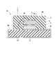
- FIG. 1 is a diagram showing an example of a light-emitting diode according to the first embodiment of the present invention.
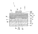
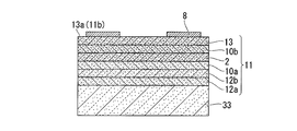
- a light emitting diode (LED) 1 according to an embodiment of the present invention includes a light emitting unit 3 including a light emitting layer 2 and a compound semiconductor layer 11 including at least a strain adjustment layer 13, and a reflective structure 4. And a metal substrate which is the functional substrate 5 bonded to the light emitting unit 3.
- the surface 3a of the light emitting unit 3 opposite to the reflective structure 4 is provided with a first electrode 6, and the surface 3b of the light emitting unit 3 on the reflective structure 4 side is provided with a strain adjustment layer 13 interposed therebetween.
- a second electrode 8 is provided.
- the light emitting unit 3 is configured by sequentially laminating at least a p-type lower cladding layer 10b, a light emitting layer 2, and an n-type upper cladding layer 10a on a strain adjustment layer 13. That is, the light emitting unit 3 includes a lower clad disposed opposite to the lower side and the upper side of the light emitting layer 2 in order to “confine” the light emission layer 2 with a carrier (carrier) that causes radiative recombination.
- DH double hetero
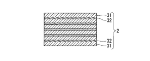
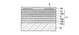
- FIG. 2 is an enlarged cross-sectional view for explaining the configuration of the light emitting unit of the light emitting diode according to the first embodiment of the present invention.
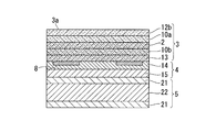
- the light emitting layer 2 preferably has a multilayer structure of a strained light emitting layer 31 and a barrier layer 32.
- the thickness of the light emitting layer 2 is preferably in the range of 0.02 to 2 ⁇ m.
- the conductivity type of the light emitting layer 2 is not particularly limited, and any of undoped, p-type and n-type can be selected. In order to increase the light emission efficiency, it is desirable that the crystallinity be undoped or the carrier concentration be less than 3 ⁇ 10 17 cm ⁇ 3 .
- the strained light emitting layer 31 has a composition of (Al X Ga 1-X ) Y In 1-YP (0 ⁇ X ⁇ 1, 0 ⁇ Y ⁇ 1).
- X is preferably 0.1 or less, and more preferably 0.
- Y is preferably in the range of 0.37 to 0.46, more preferably in the range of 0.38 to 0.46, and still more preferably in the range of 0.39 to 0.45.
- the emission wavelength can be set in the range of 655 to 675 nm.
- the strained light emitting layer 31 has a different structure from that of the other structural portions, and strain is generated in the compound semiconductor layer 2. For this reason, there is a possibility that an adverse effect of generation of crystal defects may occur.
- the layer thickness of the strained light emitting layer 31 is preferably in the range of 8 nm or more and less than 30 nm.
- the layer thickness of the strained light emitting layer 31 is desirably 8 nm or more that does not exhibit the quantum effect in consideration of the variation of the layer thickness.
- the composition of (Al X Ga 1-X ) Y In 1-YP (0 ⁇ X ⁇ 1, 0 ⁇ Y ⁇ 1) of the strained light emitting layer 31 is within the above-mentioned preferable range. May not be obtained. Further, considering the ease of controlling the layer thickness, 10 nm or more is preferable. On the other hand, if the thickness of the strained light emitting layer 31 is 30 nm or more, the amount of strain becomes too large, which is not preferable because crystal defects and surface abnormalities are likely to occur.
- the barrier layer 32 has a composition of (Al X Ga 1-X ) Y In 1-YP (0 ⁇ X ⁇ 1, 0 ⁇ Y ⁇ 1).
- X is preferably in the range of 0.3 to 0.7, more preferably in the range of 0.4 to 0.6.
- Y is preferably in the range of 0.48 to 0.52, more preferably in the range of 0.49 to 0.51.
- the lattice constant of the barrier layer 32 can be equal to or smaller than that of the GaAs substrate.
- the barrier layer 32 is preferably thicker than the strained light emitting layer 31. Thereby, the luminous efficiency of the strained light emitting layer 31 can be increased. In addition, it is necessary to optimize the light emission efficiency by the barrier layer 32 and reduce the strain generated in the strained light emitting layer 31. Therefore, the barrier layer 32 preferably has a layer thickness of at least 15 nm, more preferably 20 nm or more. On the other hand, when the thickness of the barrier layer 32 exceeds 50 nm, it becomes close to the wavelength of the emission wavelength, and optical influences such as light interference and Bragg reflection occur. Therefore, the barrier layer 32 is preferably 50 nm or less, and more preferably 40 nm or less. As described above, when the strained light emitting layer 31 is thinner and the barrier layer 32 is thicker, an effect of absorbing the strain of the strained light emitting layer 31 by the barrier layer 32 is obtained. The effect that defects are hardly generated is obtained.
- the number of pairs in which the strained light emitting layer 31 and the barrier layer 32 are alternately stacked is not particularly limited, but is 8 pairs or more and 40 pairs or less. Is preferred. That is, the light emitting layer 2 preferably includes 8 to 40 strained light emitting layers 31. Here, as a suitable range of the light emitting efficiency of the light emitting layer 2, it is preferable that the strain light emitting layer 31 is eight or more layers. On the other hand, since the strained light emitting layer 31 and the barrier layer 32 have a low carrier concentration, the forward voltage (VF) will increase if many pairs are used.
- VF forward voltage
- the strain of the strained light emitting layer 31 is stress generated in the light emitting layer 2 because the lattice constants of the GaAs substrate (not shown) and the light emitting layer 2 are different. For this reason, when the number of pairs in which the strained light emitting layers 31 and the barrier layers 32 are alternately stacked, that is, the number of the strained light emitting layers 31 included in the light emitting layer 2 exceeds the above range, the light emitting layer 2 becomes distorted. A crystal defect occurs without being able to endure, and problems such as deterioration of the surface state and reduction in luminous efficiency occur.
- the light-emitting layer 2 (light-emitting portion 3) preferably has a peak emission wavelength in the emission spectrum of 655 to 675 nm by regulating the material of the strained light-emitting layer 31 in the above range, and is more photosynthetic within this range. It is more preferable that the range of 660 to 670 nm is high.
- the emission wavelength in the above range is one of emission wavelengths suitable for light sources for plant growth (photosynthesis), and is desirable because of high reaction efficiency for photosynthesis.
- a reaction that suppresses the growth of plants occurs.
- a red light source that has strong light in the wavelength region of 655 to 675 nm, which is optimal for the photosynthetic reaction, and does not contain light in the ultrawavelength region of 700 nm or more is most preferable.
- the half width needs to be narrow.
- the half-value width is narrowed near the quantization condition that may cause a large variation in wavelength, and as a result, the half-value width of the emission spectrum is preferably in the range of 10 to 40 nm.
- the emission intensity of the emission spectrum at an emission wavelength of 700 nm is less than 10% of the emission intensity at the peak emission wavelength.
- the response speed (rise time: Tr) of the light emitting layer 2 is preferably 100 ns or less.
- the light emitting diode 1 having the light emitting layer 2 having such characteristics can be suitably used as illumination (light emitting diode lamp) used for promoting photosynthesis for plant growth.
- the composition, the layer thickness, and the number of layers of the structure of the light emitting layer 2 can be appropriately selected so as to satisfy the above characteristics.
- the lower cladding layer 10 b and the upper cladding layer 10 a are provided on one surface of the light emitting layer 2. Specifically, the lower cladding layer 10 b is provided on the lower surface of the light emitting layer 2, and the upper cladding layer 10 a is provided on the upper surface of the light emitting layer 2.
- the material of the lower cladding layer 10b and the upper cladding layer 10a is preferably a material having a larger band gap than the strained light emitting layer 31, and more preferably a material having a larger band gap than the barrier layer 32.
- the material include a compound having a composition of Al X Ga 1-X As and a composition of (Al X Ga 1-X ) Y In 1-YP (0 ⁇ X ⁇ 1, 0 ⁇ Y ⁇ 1).
- the compound which has is mentioned.
- the lower limit of the value of X is preferably 0.3 or more, and more preferably 0.5 or more.
- the value of Y is preferably in the range of 0.48 to 0.52, more preferably in the range of 0.49 to 0.51.
- the lower cladding layer 10b and the upper cladding layer 10a are configured to have different polarities.
- the carrier concentration and thickness of the lower clad layer 10b and the upper clad layer 10a can be in a known suitable range, and the conditions are preferably optimized so that the light emission efficiency of the light emitting layer 2 is increased. Further, the warpage of the compound semiconductor layer 11 can be reduced by controlling the composition of the lower cladding layer 10b and the upper cladding layer 10a.
- the lower clad layer 10b for example, Mg-doped p-type (Al X Ga 1-X ) Y In 1-YP (0.3 ⁇ X ⁇ 1, 0 ⁇ Y ⁇ 1) It is desirable to use a semiconductor material.
- the carrier concentration is preferably in the range of 2 ⁇ 10 17 to 2 ⁇ 10 18 cm ⁇ 3
- the layer thickness is preferably in the range of 0.5 to 5 ⁇ m.
- the upper clad layer 10a for example, a semiconductor made of n-type (Al X Ga 1-X ) Y In 1-YP (0.3 ⁇ X ⁇ 1, 0 ⁇ Y ⁇ 1) doped with Si is used. It is desirable to use materials.
- the carrier concentration is preferably in the range of 1 ⁇ 10 17 to 1 ⁇ 10 18 cm ⁇ 3 , and the layer thickness is preferably in the range of 0.5 to 2 ⁇ m.
- the polarities of the lower cladding layer 10b and the upper cladding layer 10a can be selected in consideration of the element structure of the compound semiconductor layer 11.
- the surface of the upper cladding layer 10a that contacts the contact layer 12b is a surface that functions as the light extraction surface 11a and is roughened (in other words, includes a rough surface). In this way, by roughening the light extraction surface 11a, total reflection on the light extraction surface 11a is suppressed, so that the light extraction efficiency can be improved.
- each intermediate layer is preferably composed of a semiconductor material having a band gap between the two layers.
- a contact layer 12b for reducing the contact resistance of the ohmic electrode is provided on the uppermost layer of the constituent layers of the light emitting unit 3.
- a current diffusion layer for planarly diffusing the element driving current over the entire light emitting portion, and conversely, a current blocking layer or current constriction for limiting the region through which the element driving current flows.
- a known layer structure such as a layer may be provided.
- the strain adjustment layer 13 is provided below the light emitting unit 3.
- the strain adjusting layer 13 is a layer for relaxing strain generated by the strained light emitting layer 31 when the compound semiconductor layer 11 is epitaxially grown on a GaAs substrate (not shown).
- the strain adjustment layer 13 is transparent to the emission wavelength of the light emitting unit 3 (light emitting layer 2).
- the strain adjusting layer 13 has a lattice constant smaller than that of the strained light emitting layer 31 and the barrier layer 32.
- the strain adjustment layer 13 has a lattice constant smaller than that of a GaAs substrate (not shown) used for forming the compound semiconductor layer 11 (formation by epitaxial growth).
- the lattice constant of the strain adjusting layer 13 obtained from the composition described later is A
- the lattice constant of the barrier layer 32 is B
- the lattice constant of the strained light emitting layer 31 is C
- a material having a composition of (Al X Ga 1-X ) Y In 1- YP (0 ⁇ X ⁇ 1, 0.6 ⁇ Y ⁇ 1) can be applied.
- X depends on the element structure of the compound semiconductor layer 11, it is preferably 0.5 or less and more preferably 0 because a material having a low Al concentration is chemically stable.
- the said lower limit of Y is 0.6 or more.
- the strain adjusting effect of the strain adjusting layer 13 becomes smaller when the value of Y is smaller. For this reason, it is necessary to increase the thickness of the strain adjustment layer 13. As a result, the growth time and cost at the time of forming the strain adjusting layer 13 increase, so the value of Y is preferably 0.6 or more, and more preferably 0.8 or more.
- the strain adjustment layer 13 is a layer that is transparent with respect to the emission wavelength of the light emitting unit 3 and is Al X Ga 1-X As 1-Y P Y (0 ⁇ X ⁇ 1, 0.6 ⁇ Y ⁇ 1).
- Group III-V semiconductor materials having the composition of) can also be suitably used.
- the lattice constant varies depending on the value of Y. The larger the Y value, the smaller the lattice constant. Further, whether or not to transmit the light of the light emitting unit 3 is related to both the values of X and Y, so if the values of X and Y are selected so as to be transparent to the light emission wavelength of the light emitting unit 3 good.
- the strain adjustment layer 13 it is preferable to use a GaP layer, preferably a p-type GaP layer doped with Mg, for example.
- the GaP layer is most suitable as the strain adjustment layer 13 from the viewpoint of productivity and stability because it does not require adjustment of the composition and has a large strain adjustment effect.
- the strain adjustment layer 13 Since the strain adjustment layer 13 has a lattice constant smaller than the lattice constant of a GaAs substrate (not shown) that is a substrate used when the light emitting unit 3 is epitaxially grown, the amount of strain included in the strain light emitting layer 31 is increased. It has a function to reduce variations. For this reason, the provision of the strain adjusting layer 13 has the effect of uniforming the characteristics such as the emission wavelength and preventing the occurrence of crystal defects such as cracks.
- the thickness of the strain adjusting layer 13 is preferably in the range of 0.5 to 20 ⁇ m, and more preferably in the range of 3 to 15 ⁇ m.
- the layer thickness is less than 0.5 ⁇ m, it is not sufficient to alleviate variation in the strain amount of the strained light emitting layer 31, and if the layer thickness exceeds 20 ⁇ m, the growth time becomes long and the manufacturing cost increases, which is not preferable. .
- the warpage of the compound semiconductor layer 11 can be reduced, and thus the light emitting diode 1 having a small in-plane wavelength distribution can be manufactured. Further, even when the functional substrate 5 and the compound semiconductor layer 11 are bonded via the reflective structure 4 as in the present embodiment, if the warpage of the compound semiconductor layer 11 is large, cracks or the like are caused. Therefore, it is desirable to reduce the warp of the compound semiconductor layer 11.
- the first electrode 6 and the second electrode 8 are ohmic electrodes, and their shape and arrangement are not particularly limited as long as the current is uniformly diffused in the light emitting unit 3.
- a circular or rectangular electrode can be used when viewed from above, and the electrodes can be arranged as a single electrode or a plurality of electrodes can be arranged in a grid.
- an n-type compound semiconductor for example, an AuGe layer, an AuSi layer or the like can be used, and a p-type compound semiconductor is used as the contact layer 12b.
- an AuBe layer, an AuZn layer, or the like can be used. Further, by further laminating an Au layer or the like thereon, oxidation can be prevented and connection reliability of wire bonding can be improved.
- an n-type compound semiconductor for example, an AuGe layer, an AuSi layer, or the like can be used, and a p-type compound is used as the strain adjustment layer 13.
- a semiconductor for example, an AuBe layer, an AuZn layer, or the like can be used.
- the reflective structure 4 is formed on the surface 13 a of the strain adjustment layer 13 so as to cover the second electrode 8.
- the reflective structure 4 has a configuration in which a transparent conductive film 14 and a reflective layer 15 are sequentially stacked.
- the transparent conductive film 14 is formed on the surface 13 a of the strain adjustment layer 13 (the surface of the strain adjustment layer 13 on which the second electrode 8 is formed) so as to cover the second electrode 8.
- the transparent conductive film 14 for example, an ITO film, an IZO film, or the like can be used.
- a so-called cold mirror using a difference in refractive index of a transparent material for example, a multilayer film of titanium oxide film, silicon oxide film, white alumina, AlN May be combined with the reflective layer 15.
- the reflective layer 15 is laminated on the transparent conductive film 14.
- the reflective layer 15 is made of a material such as a metal such as copper, silver, gold, or aluminum and an alloy thereof. These materials have high light reflectivity, and the light reflectivity from the reflective structure 4 can be 90% or more.
- the light from the light emitting layer 2 can be reflected by the reflective layer 15 in the front direction f, and the light extraction efficiency in the front direction f can be improved. Thereby, the brightness of the light emitting diode 1 can be further increased.
- the front direction f is a direction in which the angle formed with the light extraction surface 11a of the compound semiconductor layer 11 (in the present embodiment, the surface 3a of the light emitting portion 3) is 90 °, and the light emitting diode 1 The direction away from the center.
- the reflective structure 4 may be formed of only the reflective layer 15 without providing the transparent conductive film 14.
- the irradiance radiated in the direction forming an angle of 90 ° with respect to the light extraction surface 11a is radiated in the direction forming the angle of 45 ° with respect to the light extraction surface 11a. It is good to comprise so that it may become larger than 1.0 time.
- the irradiance radiated in the direction that forms an angle of 90 ° with respect to the light extraction surface 11a (the direction orthogonal to the light extraction surface 11a), and the angle of 45 ° with respect to the light extraction surface 11a.
- the intensity of light in the direction orthogonal to the light extraction surface 11a is the same as the light intensity of the light emitting diode that does not include the reflective structure 4.
- the power consumption can be made smaller than that of the light emitting diode not provided with the reflecting structure 4.
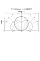
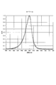
- FIG. 3 is a diagram showing the irradiance of a light emitting diode not provided with a reflecting structure and a light emitting diode provided with a reflecting structure.
- the irradiance of the light irradiated from the light extraction surface 11a is shown.
- the irradiation angle in the direction orthogonal to the light extraction surface 11a is 90 °
- the irradiation angle in the direction parallel to the light extraction surface 11a is 0 °.
- the irradiance is large in the oblique direction (specifically, the direction of the radiation angle is 15 to 55 °), and the radiation angle is from 60 ° to 90 °. It can be confirmed that the irradiance decreases as the angle approaches °.
- the irradiance is smaller than that of the light emitting diode not provided with the reflective structure 4 when the radiation angle is 60 ° or less, and the radiation angle is within the range of 60 ° to 90 °.
- the irradiation illuminance was larger than that of the light emitting diode not provided with the reflecting structure 4. From this, it was confirmed that the provision of the reflective structure 4 can increase the irradiance of light emitted in a direction that forms an angle of 90 ° with the light extraction surface 11a.
- the reflective layer 15 for example, a laminated film made of Ag alloy layer / W layer / Pt layer / Au layer / connection metal layer from the transparent conductive film 14 side can be used.
- the connection metal formed on the surface 15b of the reflective layer 15 located on the opposite side to the surface in contact with the transparent conductive film 14 a metal having low electrical resistance and melting at a low temperature may be used.
- the functional substrate 5 can be connected without applying heat stress to the light emitting section 3.
- an Au-based eutectic metal that is chemically stable and has a low melting point may be used.
- Au-based eutectic metal examples include eutectic compositions (Au-based eutectic metals) of alloys such as AuSn, AuGe, and AuSi.
- metals such as titanium, chromium, and tungsten, to the connection metal.
- a metal such as titanium, chromium or tungsten as a connecting metal, the metal functions as a barrier metal, so that impurities contained in the functional substrate 5 diffuse to the reflective layer 15 side and react. Can be suppressed.
- the functional substrate 5 is attached to the surface 11 b of the compound semiconductor layer 11 (specifically, the surface 13 a of the strain adjustment layer 13) via the reflective structure 4. Specifically, the bonding surface 5a of the functional substrate 5 is bonded to the surface 15b of the reflection structure 4 located on the opposite side to the surface of the reflection structure 4 facing the light emitting unit 3.
- a metal substrate is used as the functional substrate 5. That is, in the first embodiment, the metal substrate is attached to the surface 11 b of the compound semiconductor layer 11 (specifically, the surface 13 a of the strain adjustment layer 13) via the reflective structure 4.
- the case where a metal substrate is used as the functional substrate 5 will be described as an example.
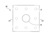
- the functional substrate 5 can be made of a plurality of metal layers. Furthermore, the functional substrate 5 is preferably configured by alternately laminating two types of metal layers. The total number of the two types of metal layers is preferably an odd number.
- the first metal layer 21 is heated more than the compound semiconductor layer 11. It is preferable to use a material having a large expansion coefficient. Thereby, since the thermal expansion coefficient of the functional substrate 5 as a whole is close to the thermal expansion coefficient of the compound semiconductor layer 11, warping and cracking of the functional substrate 5 when the compound semiconductor layer 11 and the functional substrate 5 are bonded together. Therefore, the yield of the light emitting diodes 1 can be improved.
- the first metal layer 21 is preferably made of a material having a smaller thermal expansion coefficient than the compound semiconductor layer 11.
- the thermal expansion coefficient of the functional substrate 5 as a whole becomes close to the thermal expansion coefficient of the compound semiconductor layer 11, so that the warpage of the functional substrate 5 when the compound semiconductor layer 11 and the functional substrate 5 are bonded together. Since it becomes possible to suppress a crack, the yield of the light emitting diode 1 can be improved.
- the positions of the first and second metal layers 21 and 22 constituting the functional substrate 5 can be interchanged. That is, in FIG. 1, the functional substrate 5 is configured by sandwiching one second metal layer with two first metal layers 21, but one first layer is formed by two second metal layers 22.
- the functional substrate 5 (metal substrate) may be configured by sandwiching the metal layer 21.
- a suitable example of the functional substrate 5 is a metal substrate composed of three layers of Cu layer / Mo layer / Cu layer.
- a metal substrate composed of three layers of Mo layer / Cu layer / Mo layer can achieve the same effect as a metal substrate composed of three layers of Cu layer / Mo layer / Cu layer.
- the metal substrate composed of three layers of Cu layer / Mo layer / Cu layer has a structure in which Mo having high mechanical strength is sandwiched between Cu that is easy to process, it is more than three layers of Mo layer / Cu layer / Mo layer. There is an advantage that processing such as cutting of the metal substrate can be performed more easily than the metal substrate.
- the thermal expansion coefficient of the functional substrate 5 as a whole is, for example, 6.1 ppm / K when a metal substrate composed of a Cu layer (30 ⁇ m) / Mo layer (25 ⁇ m) / Cu layer (30 ⁇ m) is used as the functional substrate 5. It becomes.
- a metal substrate composed of Mo layer (25 ⁇ m) / Cu layer (70 ⁇ m) / Mo layer (25 ⁇ m) is used as the functional substrate 5
- the thermal expansion coefficient of the functional substrate 5 as a whole is 5.7 ppm / K.
- the metal layer constituting the functional substrate 5 is preferably made of a material having high thermal conductivity. By using such a material, the heat dissipation of the functional substrate 5 can be increased, the light emitting diode 1 can emit light with high luminance, and the life of the light emitting diode 1 can be extended. it can.
- thermal conductivity 420 W / m ⁇ K
- alloys thereof are preferably used.
- the thermal expansion coefficient of the metal layer constituting the functional substrate 5 is preferably made of a material that is substantially equal to the thermal expansion coefficient of the compound semiconductor layer 11.
- the thermal expansion coefficient of the material of the metal layer constituting the functional substrate 5 is preferably within ⁇ 1.5 ppm / K of the thermal expansion coefficient of the compound semiconductor layer 11.
- the thermal conductivity of the functional substrate 5 is 250 W / m ⁇ K.
- the thermal conductivity of the functional substrate 5 is 220 W / m ⁇ K.
- the thickness of the functional substrate 5 made of a metal substrate is preferably 50 ⁇ m or more and 150 ⁇ m or less.
- the thickness of the functional substrate 5 is thicker than 150 ⁇ m, the manufacturing cost of the light emitting diode increases, which is not preferable. If the thickness of the functional substrate 5 is less than 50 ⁇ m, cracking, chipping, warping, etc. easily occur during handling, which may reduce the yield of light emitting diodes.
- the number of the first metal layer 21 and the second metal layer 22 constituting one functional substrate 5 is preferably 3 to 9 layers, more preferably 3 to 5 layers. .
- the thermal expansion in the thickness direction becomes unbalanced and the functional substrate 5 may be cracked. appear.
- the total number of layers of the first metal layer 21 and the second metal layer 22 is more than nine, the thicknesses of the first metal layer 21 and the second metal layer 22 are reduced. Each needs to be thin.
- the first metal layer 21 or the second metal layer 22 is made thin.
- the thickness of each layer becomes non-uniform, and there is a possibility that the characteristics of the light-emitting diode may vary.
- the single-layer metal substrate having a thin layer thickness easily causes the substrate to crack.
- it is difficult to manufacture the metal substrate which may increase the manufacturing cost of the light emitting diode.
- a bonding auxiliary film that stabilizes electrical contact or a eutectic metal for die bonding may be formed on the bonding surface 5a of the functional substrate 5. Thereby, a joining process can be performed simply.
- the auxiliary bonding film an Au film, an AuSn film, or the like can be used.
- the method of bonding the functional substrate 5 to the light emitting unit 3 is not limited to the above-described method, and known techniques such as diffusion bonding, an adhesive, and a room temperature bonding method can be applied.
- the light emitting unit 3 includes the compound semiconductor layer 11 including at least the pn junction type light emitting unit 3 and the strain adjustment layer 8 stacked on the light emitting unit 3.
- the light emitting diode 1 having an emission wavelength of 655 nm or more can be realized. Further, by providing the strain adjusting layer 13 that transmits the light of the light emitting unit 3 on the light emitting unit 3, the light from the light emitting unit 3 is not absorbed by the strain adjusting layer 13, so that high output and high efficiency are achieved. The light emitting diode 1 can be realized.
- the strain adjusting layer 13 has a lattice constant smaller than the lattice constants of the strained light emitting layer 31 and the barrier layer 32, the occurrence of warpage of the semiconductor compound layer 11 can be suppressed. Thereby, since the variation in the strain amount of the strained light emitting layer 31 is reduced, the light emitting diode 1 having excellent monochromaticity can be realized. Further, the reflective structure 4 is provided on the surface 11b of the compound semiconductor layer 11 located on the opposite side to the light extraction surface 11a of the compound semiconductor layer 11, so that the light emitting diode 1 of the light emitting diode 1 is removed from the light extraction surface 11a of the compound semiconductor layer 11.
- the intensity of light in the direction orthogonal to the light extraction surface 11a (specifically, the front direction f).
- the diode 1 can be realized. Further, by increasing the intensity of light in the direction orthogonal to the light extraction surface 11a, the intensity of light in the direction orthogonal to the light extraction surface 11a is the same as the light intensity of the light emitting diode that does not include the reflective structure 4. In the case of obtaining a strong light intensity, the power consumption can be made smaller than that of the light emitting diode not provided with the reflecting structure 4.
- the functional substrate 5 is constituted by the first and second metal layers 21 and 22 having a thermal conductivity of 130 W / m ⁇ K or more, the heat dissipation of the functional substrate 5 is increased, so that the light emitting diode 1 can emit light with high luminance, and the life of the light-emitting diode 1 can be extended.
- the bonding surface has a high resistance and it is difficult to pass a current to the substrate side.
- the light emitting diode of the first embodiment it has a red light emission wavelength of 655 nm or more, is excellent in monochromaticity, has high output and high efficiency, has a high response speed, and has a light extraction surface.
- the light emitting diode 1 having high light intensity in the orthogonal direction and excellent heat dissipation characteristics.
- 4A to 10 are cross-sectional views showing manufacturing steps of the light emitting diode according to the first embodiment of the present invention.
- 4A to 10 the same components as those of the light emitting diode 1 shown in FIG. 1 are denoted by the same reference numerals.
- FIGS. 4A to 10 a method for manufacturing the light-emitting diode 1 of the first embodiment will be described. First, the manufacturing process of the functional substrate 5 will be described.
- the functional substrate 5 is formed by hot pressing the first and second metal layers 21 and 22 having a thermal conductivity of 130 W / m ⁇ K or more.
- first metal layers 21 and one substantially flat second metal layer 22 are prepared.
- a Cu layer having a thickness of 30 ⁇ m is used as the first metal layer 21
- a Mo layer having a thickness of 25 ⁇ m is used as the second metal layer 22.
- the second metal layer 22 is inserted between the two first metal layers 21 and these are stacked.
- a laminated plate in which the first and second metal layers 21 and 22 are stacked is disposed in a predetermined pressurizing apparatus, and the first metal layer 21 and the second metal layer 22 are placed at a high temperature.
- a pressure is applied in the direction of the arrow (see FIG. 4A), and then crimped. 4B, the first metal layer 21 is a Cu layer, the second metal layer 22 is a Mo layer, and a Cu layer (30 ⁇ m) / Mo layer (25 ⁇ m) / Cu layer (30 ⁇ m).
- the functional substrate 5 consisting of three layers is formed.
- the functional substrate 5 configured as described above had a thermal expansion coefficient of 6.1 ppm / K and a thermal conductivity of 250 W / m ⁇ K.
- a bonding auxiliary film may be formed on the bonding surface 5a of the functional substrate 5 in order to stabilize electrical contact.
- a gold film, a platinum film, a nickel film, or the like can be used as the auxiliary bonding film.
- a nickel film is first formed to a thickness of 0.1 ⁇ m, and then a gold film is formed to a thickness of 0.5 ⁇ m on the nickel film.
- a eutectic metal film such as an AuSn film for die bonding may be formed instead of the above-mentioned bonding auxiliary film. Thereby, a joining process can be simplified.
- the semiconductor substrate 33 is a substrate on which the compound semiconductor layer 11 is formed.
- the semiconductor substrate 33 is a Si-doped n-type GaAs single crystal substrate having a surface 33a inclined by 15 ° from the (100) plane.
- a gallium arsenide (GaAs) single crystal substrate is preferably used as the substrate on which the compound semiconductor layer 11 is formed.
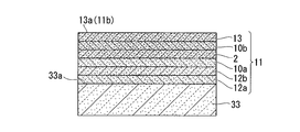
- the compound semiconductor layer 11 is formed on a GaAs substrate, which is a semiconductor substrate 33, a buffer layer 12a made of GaAs, an etching stop layer (not shown) provided for selective etching, and an n-type AlGaInP doped with Si.
- the contact layer 12b made of n-type, the n-type upper clad layer 10a, the light emitting layer 2, the p-type lower clad layer 10b, and the strain adjusting layer 13 made of Mg-doped p-type GaP are sequentially laminated.
- the GaAs substrate a commercially available single crystal substrate manufactured by a known manufacturing method can be used.
- the surface on which the GaAs substrate is epitaxially grown is preferably smooth.
- the surface orientation of the surface of the GaAs substrate is easily epi-grown, and the (100) plane and (100) that are mass-produced are preferred from the standpoint of quality stability to substrates that are off within ⁇ 20 °.
- the range of the plane orientation of the GaAs substrate is more preferably 15 ° off ⁇ 5 ° from the (100) direction to the (0-1-1) direction.
- the dislocation density of the GaAs substrate is desirably low in order to improve the crystallinity of the compound semiconductor layer 11. Specifically, for example, 10,000 pieces cm ⁇ 2 or less, preferably 1,000 pieces cm ⁇ 2 or less are suitable.
- the GaAs substrate may be n-type or p-type.
- the carrier concentration of the GaAs substrate can be appropriately selected from desired electrical conductivity and element structure.
- the carrier concentration is preferably in the range of 1 ⁇ 10 17 to 5 ⁇ 10 18 cm ⁇ 3 .
- the carrier concentration is preferably in the range of 2 ⁇ 10 18 to 5 ⁇ 10 19 cm ⁇ 3 .
- the thickness of the GaAs substrate has an appropriate range depending on the size of the substrate. If the thickness of the GaAs substrate is thinner than an appropriate range, the compound semiconductor layer 11 may be broken during the manufacturing process. On the other hand, if the thickness of the GaAs substrate is thicker than the appropriate range, the material cost increases. For this reason, when the substrate size of the GaAs substrate is large, for example, when the diameter is 75 mm, a thickness of 250 to 500 ⁇ m is desirable to prevent cracking during handling. Similarly, when the diameter is 50 mm, a thickness of 200 to 400 ⁇ m is desirable, and when the diameter is 100 mm, a thickness of 350 to 600 ⁇ m is desirable.
- warping of the compound semiconductor layer 11 can be reduced by increasing the thickness of the substrate according to the substrate size of the GaAs substrate.
- the shape of the GaAs substrate is not particularly limited to a circle, and there is no problem even if it is a rectangle or the like.
- the buffer layer 12 a is provided to alleviate a lattice mismatch between the semiconductor substrate 33 and the constituent layers of the light emitting unit 3. For this reason, if the quality of the substrate and the epitaxial growth conditions are selected, the buffer layer 12a is not necessarily required.
- the buffer layer 12a is preferably made of the same material as that of the substrate to be epitaxially grown. Therefore, in this embodiment, it is preferable to use a GaAs layer made of the same material as the GaAs substrate for the buffer layer 12a.
- the buffer layer 12a can also be a multilayer film made of a material different from that of the GaAs substrate in order to reduce the propagation of defects.
- the thickness of the buffer layer 12a is preferably 0.1 ⁇ m or more, and more preferably 0.2 ⁇ m or more.
- the contact layer 12b is provided to reduce the contact resistance with the electrode.
- the material of the contact layer 12b is preferably a material having a band gap larger than that of the strained light emitting layer 31, and Al X Ga 1-X As, (Al X Ga 1-X ) Y In 1-YP (0 ⁇ X ⁇ 1,0 ⁇ Y ⁇ 1) is preferred.
- the lower limit value of the carrier concentration of the contact layer 12b is preferably 5 ⁇ 10 17 cm ⁇ 3 or more and more preferably 1 ⁇ 10 18 cm ⁇ 3 or more in order to reduce the contact resistance with the electrode.
- the upper limit value of the carrier concentration is desirably 2 ⁇ 10 19 cm ⁇ 3 or less at which the crystallinity is likely to decrease.
- the thickness of the contact layer 12b is preferably 0.5 ⁇ m or more, and optimally 1 ⁇ m or more.
- the upper limit value of the thickness of the contact layer 12b is not particularly limited, but is desirably 5 ⁇ m or less in order to bring the cost for epitaxial growth to an appropriate range.
- the compound semiconductor layer 11 of the present embodiment can be formed using a known growth method such as molecular beam epitaxy (MBE) or reduced pressure metal organic chemical vapor deposition (MOCVD). Among these, it is desirable to apply the MOCVD method which is excellent in mass productivity. Specifically, a GaAs substrate (semiconductor substrate 33) used for the epitaxial growth of the compound semiconductor layer 11 is subjected to a pretreatment such as a cleaning process or a heat treatment before the growth to remove surface contamination or a natural oxide film. Is desirable. Each of the layers constituting the compound semiconductor layer 11 can be laminated by setting eight or more GaAs substrates 14 having a diameter of 50 to 150 mm in an MOCVD apparatus and simultaneously epitaxially growing them. As the MOCVD apparatus, a commercially available large-sized apparatus such as a self-revolving type or a high-speed rotating type can be applied.
- MBE molecular beam epitaxy
- MOCVD reduced pressure metal organic chemical vapor deposition
- examples of the group III constituent material include trimethylaluminum ((CH 3 ) 3 Al), trimethylgallium ((CH 3 ) 3 Ga), and trimethylindium ((CH 3 ) 3 In) can be used.
- a Mg doping material for example, biscyclopentadienyl magnesium (bis- (C 5 H 5 ) 2 Mg) or the like can be used.
- a Si doping material for example, disilane (Si 2 H 6 ) or the like can be used.
- phosphine (PH 3 ), arsine (AsH 3 ), or the like can be used as a raw material for the group V constituent element.
- each layer can be 720 to 770 ° C. when a p-type GaP layer is used as the strain adjustment layer 13, and 600 to 700 ° C. can be applied to the other layers. Furthermore, the carrier concentration, layer thickness, and temperature conditions of each layer can be selected as appropriate.
- the compound semiconductor layer 11 manufactured in this way has a good surface state with few crystal defects despite having the strained light emitting layer 31.
- the surface 13a of the strain adjustment layer 13 opposite to the semiconductor substrate 33 is mirror-polished to a depth of 1 ⁇ m from the surface, so that the surface roughness is within 0.18 nm, for example.
- the second electrode 8 (ohmic electrode) is formed on the surface 13 a of the strain adjustment layer 13.
- the second electrode 8 is formed by laminating an Au layer having a thickness of 0.2 ⁇ m on an AuBe layer having a thickness of 0.4 ⁇ m.
- the second electrode 8 has a circular shape of 20 ⁇ m ⁇ when viewed in plan, and is formed at intervals of 60 ⁇ m.
- a transparent conductive film 14 made of an ITO film is formed so as to cover the surface 13 a opposite to the semiconductor substrate 33 of the strain adjustment layer 13 and the second electrode 8.
- a heat treatment at 450 ° C. is performed to form an ohmic contact between the second electrode 8 and the transparent conductive film 14.
- the reflective layer 15 is formed on the surface 14 a of the transparent conductive film 14 on the side opposite to the compound semiconductor layer 11 by using a vapor deposition method. Specifically, a film (thickness: 0.5 ⁇ m) made of a silver (Ag) alloy, a tungsten (W) film (thickness: 0.1 ⁇ m), and a platinum (Pt) film (thickness: 0.1 ⁇ m) ), A gold (Au) film (thickness: 0.5 ⁇ m), and a film (thickness: 1 ⁇ m) made of AuGe eutectic metal (melting point: 386 ° C.) are sequentially formed to form the reflective layer 15. Thereby, the reflective structure 4 including the reflective layer 15 and the transparent conductive film 14 is formed.
- a conductive film for an electrode which is a base material of the first electrode 6 (n-type ohmic electrode), is formed on the surface 3a of the light emitting section 3 on the side opposite to the reflective structure 4 using a vacuum deposition method.
- the electrode conductive film for example, a metal layer structure composed of AuGe layer / Ni layer / Au layer can be used.
- AuGe layer Ga mass ratio 12% with a thickness of 0.15 ⁇ m
- a Ni layer is formed with a thickness of 0.05 ⁇ m
- an Au layer is further formed with a thickness of 1 ⁇ m.
- the first electrode 6 is formed by patterning the electrode conductive film into a circular shape in plan view using a general photolithography means. Thereafter, the contact layer 12b is patterned so as to correspond to the shape of the first electrode 6, whereby the light emitting diode 1 shown in FIG. 1 is manufactured.
- the conductive film for electrodes for example, it is preferable to perform heat treatment at 420 ° C. for 3 minutes to alloy each metal constituting the first electrode 6. Thereby, the resistance of the first electrode 6 that is an n-type ohmic electrode can be reduced.
- the light emitting portion 3 at the cut portion that partitions the light emitting diode 1 into a desired size is removed by etching, and then the substrate and the connection layer of the cut portion are formed at a desired size using a laser at a pitch of 0.8 mm. Cut into light emitting diode chips (LED chips).
- LED chips light emitting diode chips
- the size of the light emitting diode for example, the length of the diagonal line of the substantially rectangular light emitting portion 3 when viewed in plan is 1.1 mm.
- the exposed surface of the light emitting unit 3 is protected with an adhesive sheet, and the cut surface is washed.
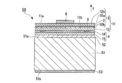
- FIG. 11 is a schematic cross-sectional view of a light-emitting diode lamp including the light-emitting diode shown in FIG. 11, the same components as those of the light-emitting diode lamp 1 shown in FIG.
- the light emitting diode lamp 40 according to the first embodiment is mounted on a package substrate 45, two electrode terminals 43 and 44 formed on the package substrate 45, and the electrode terminal 44.
- the light-emitting diode 1 includes a sealing resin 41 made of silicon or the like and formed so as to cover the light-emitting diode 1 and having light transmittance.
- the light-emitting diode 1 includes the light-emitting portion 3, the reflective structure portion 4, the functional substrate 5, the first electrode 6, and the second electrode 8.
- the conductive substrate 5 is disposed so as to be connected to the electrode terminal 43.
- the first electrode 6 is connected to the electrode terminal 44 by wire bonding.
- the voltage applied to the electrode terminals 43 and 44 is applied to the light emitting unit 3 through the first electrode 6 and the second electrode 8, so that the light emitting unit 3 is
- the light emitting layer 2 which comprises is light-emitted. The emitted light is extracted in the front direction f through the light extraction surface 11 a of the light emitting diode 1.
- the package substrate 45 has a thermal resistance of 10 ° C./W or less. Thereby, even when 1 W or more of electric power is applied to the light emitting layer 2 to emit light, the package substrate 45 can be used as a heat dissipation substrate, and the heat dissipation of the light emitting diode 1 can be further enhanced.
- the shape of the package substrate 45 is not limited to the shape shown in FIG. 11 and may be other shapes. Also in LED lamp products using package substrates of other shapes, sufficient heat dissipation can be ensured, so that a light-emitting diode lamp with high output and high brightness can be obtained.
- the light emitting diode lamp of the first embodiment light emission having the reflecting structure 4 that reflects light on the surface 11b of the compound semiconductor layer 11 located on the opposite side to the light extraction surface 11a of the compound semiconductor layer 11.
- the diode 1 By providing the diode 1, the irradiance radiated in the direction forming an angle of 90 ° with respect to the light extraction surface 11a and the irradiance radiated in the direction forming an angle of 45 ° with respect to the light extraction surface 11a. Since it becomes possible to make it larger than 1.0 times, the light-emitting diode lamp 40 with high luminance and high efficiency can be realized.
- the functional substrate 5 constituting the light emitting diode 1 is connected to the electrode terminal 43 formed on the package substrate 45 functioning as a heat dissipation substrate, whereby the light emitting diode is connected via the electrode terminal 43 and the package substrate 45. 1 heat can be released efficiently.
- the light emitting diode lamp 40 includes the package substrate 45 having a thermal resistance of 10 ° C./W or less, so that it has excellent heat dissipation and can emit light with high brightness by applying a high voltage. Further, since the light emitting diode package 40 is configured to emit light by applying power of 1 W or more to the light emitting layer 2 of the light emitting diode 1, it is excellent in heat dissipation and can emit light with high luminance by applying a high voltage.
- FIGS. 12A and 12B are views for explaining a light emitting diode according to a second embodiment of the present invention
- FIG. 12A is a plan view of the light emitting diode of the second embodiment
- FIG. It is a schematic sectional drawing of the AA 'line direction of the light emitting diode shown to 12A.
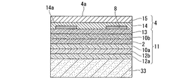
- a light emitting diode 50 according to the second embodiment includes a functional substrate 5 (metal substrate) instead of the functional substrate 5 (metal substrate) provided in the light emitting diode 1 according to the first embodiment.
- the functional substrate 51 made of a material different from that of the (metal substrate) is provided, the metal layers 52 and 53 are further provided, and the contact layer 12b is disposed so as to cover the upper surface of the upper cladding layer 10a.
- the configuration is the same as the light emitting diode 1 of the embodiment. That is, the major difference between the light emitting diode 50 of the second embodiment and the light emitting diode 1 of the first embodiment is that the material of the functional substrate is different.
- the functional substrate 51 is bonded via a metal layer 52 to the reflective structure 4 (specifically, the reflective layer 15) provided with the compound semiconductor layer 11.
- the material of the functional substrate 51 any material of GaP, Si, and Ge can be used.
- the heat generated when the light emitting unit 3 emits light compared to a light emitting diode that does not include the functional substrate 51.
- the heat can be efficiently radiated to the outside of the light emitting diode 50.
- the moisture resistance of the functional substrate 51 can be improved by using Si, Ge, or the like, which is not easily corroded, as the material of the functional substrate 51.
- the metal layer 52 is provided between the reflective layer 15 constituting the reflective structure 4 and the upper surface 51 a of the functional substrate 51.
- the metal layer 52 is a layer for joining the reflective layer 15 and the upper surface 51 a of the functional substrate 51.
- As the metal layer 52 for example, a laminated film in which an In layer, an Au layer, and a Ti layer are sequentially laminated can be used.
- the metal layer 53 is provided on the lower surface 51 b of the functional substrate 51.
- a laminated film in which an Au layer and a Ti layer are sequentially laminated can be used.
- the metal semiconductor layer 52 is joined to the reflective structure 4 provided with the compound semiconductor layer 11 and is made of any material of GaP, Si, and Ge.
- the functional substrate 51 heat generated when the light emitting unit 3 emits light can be efficiently radiated to the outside of the light emitting diode 50 as compared with a light emitting diode that does not include the functional substrate 51.
- the moisture resistance of the functional substrate 51 can be improved by using Si, Ge, or the like, which is not easily corroded, as the material of the functional substrate 51.
- the reflective structure 4 is provided on the surface 11b of the compound semiconductor layer 11 located on the opposite side to the light extraction surface 11a of the compound semiconductor layer 11, so that the light emitting diode 1 of the light emitting diode 1 is removed from the light extraction surface 11a of the compound semiconductor layer 11.
- the light emitted to the outside it is possible to increase the intensity of light in a direction orthogonal to the light extraction surface 11a (specifically, the front direction f).
- the diode 50 can be realized.
- the light emitting diode 50 of the second embodiment is composed of the composition formula (Al X Ga 1-X ) Y In 1- YP (0 ⁇ X ⁇ 0.1, 0.37 ⁇ Y ⁇ 0.46). Since the light emitting unit 3 having the laminated structure of the strained light emitting layer 31 and the barrier layer 32 is provided, the light emission efficiency and response speed of the light emitted from the light emitting unit 3 can be improved. Further, by defining the composition of the strained light emitting layer 31 in the above range, the light emitting diode 1 having an emission wavelength of 655 nm or more can be realized. Further, since the strain adjustment layer 13 that transmits the light of the light emitting unit 3 is provided on the light emitting unit 3, the light from the light emitting unit 3 is not absorbed by the strain adjusting layer 13. The light emitting diode 50 can be realized.
- the strain adjusting layer 13 has a lattice constant smaller than the lattice constants of the strained light emitting layer 31 and the barrier layer 32, the occurrence of warpage of the semiconductor compound layer 11 can be suppressed. Thereby, since the variation in the strain amount of the strained light emitting layer 31 is reduced, the light emitting diode 50 having excellent monochromaticity can be realized.
- a light emitting diode according to the present invention is manufactured. After the light emitting diode was manufactured, a light emitting diode lamp having a light emitting diode chip mounted on a substrate was prepared for characteristic evaluation.
- Example 1 In the light emitting diode of the first embodiment (first embodiment), first, compound semiconductor layers are sequentially stacked on a GaAs substrate (thickness: about 0.5 ⁇ m) made of n-type GaAs single crystal doped with Si. An epitaxial wafer was produced. In the GaAs substrate, the plane inclined by 15 ° from the (100) plane in the (0-1-1) direction was used as the growth plane, and the carrier concentration was set to 2 ⁇ 10 18 cm ⁇ 3 . Further, the compound semiconductor layer is composed of an n-type buffer layer made of GaAs doped with Si on a GaAs substrate and (Al 0.7 Ga 0.3 ) 0.5 In 0.5 P doped with Si.
- an n-type contact layer an n-type upper cladding layer made of Si-doped (Al 0.7 Ga 0.3 ) 0.5 In 0.5 P, and undoped Ga 0.44 In 0.56 P / (Al 0.53 Ga 0.47 ) 0.5 In 0.5 P pair strained light emitting layer / barrier layer and Mg-doped (Al 0.7 Ga 0.3 ) 0.5 In 0 .5 a lower cladding layer of p-type consisting of P, (Al 0.5 Ga 0.5) 0.5 in 0.5 an intermediate layer of a thin film made of P, strain adjustment layer composed of p-type GaP that Mg-doped Were sequentially formed.
- Example 1 an epitaxial wafer was formed by epitaxially growing a compound semiconductor layer on a GaAs substrate having a diameter of 76 mm and a thickness of 350 ⁇ m using a low pressure metal organic chemical vapor deposition apparatus method (MOCVD apparatus).
- MOCVD apparatus metal organic chemical vapor deposition apparatus method
- trimethylgallium ((CH 3 ) 3 Ga) and trimethylindium ((CH 3 ) 3 In) are used as the raw materials for the group III constituent elements did.
- biscyclopentadienyl magnesium bis- (C 5 H 5 ) 2 Mg) was used as a Mg doping material.
- disilane Si 2 H 6
- phosphine PH 3
- arsine AsH 3
- the strain adjustment layer made of p-type GaP was grown at 750 ° C. The other layers were grown at 700 ° C.
- the buffer layer made of GaAs has a carrier concentration of about 2 ⁇ 10 18 cm ⁇ 3 and a layer thickness of about 0.5 ⁇ m.
- the contact layer had a carrier concentration of about 2 ⁇ 10 18 cm ⁇ 3 and a layer thickness of about 3.5 ⁇ m.
- the upper cladding layer had a carrier concentration of about 1 ⁇ 10 18 cm ⁇ 3 and a layer thickness of about 0.5 ⁇ m.
- 23 strained light emitting layers (single layer thickness: 17 nm) made of undoped Ga 0.44 In 0.56 P and a composition of (Al 0.53 Ga 0.47 ) 0.
- a light emitting layer was formed by alternately stacking 22 barrier layers (single layer thickness: 19 nm) of 5 In 0.5 P.
- the lower cladding layer had a carrier concentration of about 8 ⁇ 10 17 cm ⁇ 3 and a layer thickness of about 0.5 ⁇ m.
- the intermediate layer had a carrier concentration of about 8 ⁇ 10 17 cm ⁇ 3 and a layer thickness of about 0.05 ⁇ m.
- the strain adjusting layer made of GaP has a carrier concentration of about 3 ⁇ 10 18 cm ⁇ 3 and a layer thickness of about 9 ⁇ m.
- the strain adjusting layer was polished to a region extending from the surface to a depth of about 1 ⁇ m and mirror-finished. By this mirror finishing, the surface roughness of the strain adjustment layer was set to 0.18 nm.
- an AuBe layer thinness 100 nm
- an Au layer thinness 150 nm
- the second electrode was formed by patterning the AuBe / Au laminated film using the etching technique.
- an ITO film (thickness 300 nm) as a transparent conductive film covering the second electrode, and an Ag alloy (thickness 500 nm) / W (thickness 100 nm) / Pt (thickness 200 nm) as a reflective layer ) / Au (thickness: 500 nm) / AuGe (thickness: 1000 nm) laminated film is sequentially formed to form a reflective structure.
- a functional substrate metal substrate (heat conduction) having a three-layer structure (thickness 85 ⁇ m) of Cu (30 ⁇ m) / Mo (25 ⁇ m) / Cu (30 ⁇ m) is used.
- the functional substrate of Example 1 had a thermal expansion coefficient of 6.1 ppm / K and a thermal conductivity of 250 W / m ⁇ K.
- the functional substrate had a diameter of 76 mm and a thickness of 250 ⁇ m.
- a weight of 100 g / cm 2 is applied in a state where the GaAs substrate and the functional substrate are heated to 400 ° C.
- the bonded structure was formed by bonding to the substrate.
- the GaAs substrate and the GaAs buffer layer were selectively removed from the bonded structure with an ammonia-based etchant.
- an Au—Ge—Ni alloy film having a thickness of 0.5 ⁇ m, a Pt film having a thickness of 0.2 ⁇ m, and an Au film having a thickness of 1 ⁇ m are formed on the surface of the contact layer by vacuum deposition. Films were sequentially formed.
- the Au-Ge-Ni alloy film, the Pt film, and the Au film were patterned using a general photolithography technique and an etching technique, thereby forming an n-type ohmic electrode as the first electrode.
- the contact layer was patterned by a known method so as to correspond to the shape of the first electrode.
- the surface of the light extraction surface which is the surface from which the GaAs substrate was removed, was roughened.
- the epi layer in the region where the p-type ohmic electrode is formed as the second electrode was selectively removed to expose the strain adjustment layer.
- a 0.2 ⁇ m thick AuBe film and a 1 ⁇ m thick Au film are sequentially formed on the exposed surface of the strain adjustment layer by vacuum deposition, and then the AuBe film and the Au film are patterned.
- a second electrode (p-type ohmic electrode) was formed. Thereafter, heat treatment was performed at 450 ° C. for 10 minutes to form an alloy, and low resistance first and second electrodes (n-type and p-type ohmic electrodes) were formed.
- Example 1 the light emitting diode of Example 1 was produced.
- 100 light emitting diode lamps each having the light emitting diode chip of Example 1 fabricated by the above method mounted on a mounting substrate were assembled.
- the mount is heated and connected (mounted) with a eutectic die bonder, and the n-type ohmic electrode of the light emitting diode and the n electrode terminal provided on the surface of the mounting substrate are wire-bonded with a gold wire,
- the p-type ohmic electrode and the p-electrode terminal were wire-bonded with a gold wire and then sealed with a general epoxy resin.
- Vf The forward voltage (Vf) when a current of 20 milliamperes (mA) flows in the forward direction is low in resistance at the junction interface between the strain adjustment layer and the functional substrate constituting the compound semiconductor layer, and Reflecting the good ohmic characteristics of each ohmic electrode, it was 2.1 volts (V).
- the variation in peak emission wavelength (maximum-minimum) in all assembled light-emitting diodes was 2.1 nm, and good results were obtained. Note that the variation in peak emission wavelength (maximum-minimum) may be 3 nm or less. Moreover, the response speed (Tr) of the rise of light emission was 72 ns, and good results of 100 ns or less were obtained. Also, no surface defects were found in the surface defect inspection.
- the irradiance E radiated in a direction forming an angle of 90 ° with respect to the light extraction surface is divided by the irradiance F radiated in a direction forming an angle of 45 ° with respect to the light extraction surface.
- the light emitting diode of Example 1 emitted light, no decrease in light emission efficiency due to temperature increase was observed due to the heat dissipation effect of the functional substrate.
- FIG. 13 is a diagram showing an emission spectrum of the light-emitting diode lamp of the first embodiment of the present invention. As shown in FIG. 13, the emission spectrum of the light-emitting diode lamp of Example 1 had a half-value width of 18 nm and an emission intensity at a wavelength of 700 nm was almost zero.
- Example 2 The light-emitting diode of Example 2 (second embodiment) is a 21-layer strained light-emitting layer made of undoped Ga 0.42 In 0.58 P, instead of the light-emitting layer provided in the light-emitting diode of Example 1.
- Single layer thickness 10 nm and 20 barrier layers (single layer thickness 30 nm) having a composition of (Al 0.53 Ga 0.47 ) 0.5 In 0.5 P are alternately stacked.
- a light emitting layer was formed and manufactured in the same manner as the light emitting diode of Example 1, except that a 150 ⁇ m thick GaP layer (thermal conductivity 110 W / mK) was used as the functional substrate.
- the forward voltage (Vf) when a current of 20 milliamperes (mA) flows in the forward direction is low in resistance at the junction interface between the strain adjustment layer and the functional substrate constituting the compound semiconductor layer, and Reflecting the good ohmic characteristics of each ohmic electrode, it was 2.1 volts (V).
- the light emission output when the forward current was 20 mA was 3.6 mW (3 mW or more), and a good result was obtained. ).
- the peak emission wavelength variation (maximum-minimum) of all assembled light emitting diodes was 2.3 nm, and good results were obtained.
- the response speed (Tr) of the rise of light emission was 70 ns, and good results of 100 ns or less were obtained. Also, no surface defects were found in the surface defect inspection.
- the light emitting diode of Example 2 emitted light, no decrease in light emission efficiency due to temperature increase was observed due to the heat dissipation effect of the functional substrate.
- Example 3 The light-emitting diode of Example 3 (second embodiment) is a 21-layer strained light emission made of undoped Ga 0.41 In 0.59 P instead of the strained light-emitting layer provided in the light-emitting diode of Example 2.
- a layer single layer thickness: 15 nm
- a Ge layer thermal conductivity 60 W / mK having a thickness of 100 ⁇ m was used as the functional substrate. did.
- Vf The forward voltage (Vf) when a current of 20 milliamperes (mA) flows in the forward direction is low in resistance at the junction interface between the strain adjustment layer and the functional substrate constituting the compound semiconductor layer, and Reflecting the good ohmic characteristics of each ohmic electrode, it was 2.1 volts (V).
- the variation in peak emission wavelength (maximum-minimum) in all assembled light-emitting diodes was 2.5 nm, and good results were obtained. Further, the response speed (Tr) of the rise of light emission was 73 ns, and a good result of 100 ns or less was obtained. Also, no surface defects were found in the surface defect inspection.
- the light emitting diode of Example 3 emitted light, no reduction in light emission efficiency due to temperature increase was observed due to the heat dissipation effect of the functional substrate.
- Example 4 The light-emitting diode of Example 4 (second embodiment) is a 21-layer strained light emission made of undoped Ga 0.45 In 0.55 P, instead of the strained light-emitting layer provided in the light-emitting diode of Example 2. Fabricated in the same manner as the light-emitting diode of Example 2, except that a layer (single layer thickness of 25 nm) was formed and a 100 ⁇ m thick Si layer (thermal conductivity 126 W / mK) was used as the functional substrate. did.
- the forward voltage (Vf) when a current of 20 milliamperes (mA) flows in the forward direction is low in resistance at the junction interface between the strain adjustment layer and the functional substrate constituting the compound semiconductor layer, and Reflecting the good ohmic characteristics of each ohmic electrode, it was 2.1 volts (V).
- the light emission output when the forward current was 20 mA was 4.0 mW (3 mW or more), and good results were obtained.
- the peak emission wavelength variation (maximum-minimum) of all the assembled light-emitting diodes was 2.1 nm, and good results were obtained. Further, the response speed (Tr) of the rise of light emission was 64 ns, and good results of 100 ns or less were obtained. Also, no surface defects were found in the surface defect inspection.
- the light emitting diode of Example 4 emitted light no decrease in light emission efficiency due to temperature increase was observed due to the heat dissipation effect of the functional substrate.
- Example 5 In the light-emitting diode of Example 5 (first embodiment), the composition of the strained light-emitting layer provided in the light-emitting diode of Example 2 was changed to Ga 0.39 In 0.61 P, and Cu (30 ⁇ m) / Similar to the light-emitting diode of Example 2, except that a functional substrate (metal substrate (thermal conductivity 250 W / mK)) having a three-layer structure (thickness 85 ⁇ m) of Mo (25 ⁇ m) / Cu (30 ⁇ m) was used. Manufactured.
- metal substrate thermal conductivity 250 W / mK
- Vf The forward voltage (Vf) when a current of 20 milliamperes (mA) flows in the forward direction is low in resistance at the junction interface between the strain adjustment layer and the functional substrate constituting the compound semiconductor layer, and Reflecting the good ohmic characteristics of each ohmic electrode, it was 2.1 volts (V).
- the peak emission wavelength variation (maximum-minimum) of all the assembled light-emitting diodes was 2.9 nm, and good results were obtained. Further, the response speed (Tr) of the rise of light emission was 63 ns, and good results of 100 ns or less were obtained. Also, no surface defects were found in the surface defect inspection.
- the irradiance E radiated in a direction forming an angle of 90 ° with respect to the light extraction surface is divided by the irradiance F radiated in a direction forming an angle of 45 ° with respect to the light extraction surface.
- the light emitting diode of Example 5 emitted light, no decrease in light emission efficiency due to temperature increase was observed due to the heat dissipation effect of the functional substrate.
- Example 6 The light emitting diode of Example 6 (first embodiment) is the same as that of Example 5 except that the composition of the strained light emitting layer provided in the light emitting diode of Example 5 was changed to Ga 0.38 In 0.62 P. It was manufactured in the same manner as the light emitting diode.
- Vf The forward voltage (Vf) when a current of 20 milliamperes (mA) flows in the forward direction is low in resistance at the junction interface between the strain adjustment layer and the functional substrate constituting the compound semiconductor layer, and Reflecting the good ohmic characteristics of each ohmic electrode, it was 2.1 volts (V).
- the variation in peak emission wavelength (maximum-minimum) in all assembled light-emitting diodes was 2.9 nm, and good results were obtained. Further, the response speed (Tr) of the rise of light emission was 65 ns, and good results of 100 ns or less were obtained. Also, no surface defects were found in the surface defect inspection.
- the light emitting diode of Example 6 emitted light, no decrease in light emission efficiency due to temperature increase was observed due to the heat dissipation effect of the functional substrate.
- the light emitting diode of Reference Example 1 removes the reflective structure from the configuration of the light emitting diode of Example 2, and replaces the strained light emitting layer provided in the light emitting diode of Example 2 with Ga 0.38 In 0. It was manufactured in the same manner as the light-emitting diode of the second example except that 21 strained light-emitting layers (single layer thickness: 5 nm) made of 62 P were formed. That is, the light emitting diode of Reference Example 1 does not have a reflective structure.
- the forward voltage (Vf) when a current of 20 milliamperes (mA) flows in the forward direction is low in resistance at the junction interface between the strain adjusting layer and the functional substrate constituting the compound semiconductor layer, and Reflecting the good ohmic characteristics of each ohmic electrode, it was 2.0 volts (V).
- the light emission output when the forward current was 20 mA was 3.1 mW (3 mW or more), and a good result was obtained.
- the irradiance E radiated in a direction forming an angle of 90 ° with respect to the light extraction surface is divided by the irradiance F radiated in a direction forming an angle of 45 ° with respect to the light extraction surface.
- Reference Example 2 removes the reflective structure from the structure of the light emitting diode of Example 2, and replaces the strained light emitting layer provided in the light emitting diode of Example 2 with Ga 0.37 In 0. It was manufactured in the same manner as the light emitting diode of the second example, except that 21 strained light emitting layers (single layer thickness: 10 nm) made of 63 P were formed. That is, the light emitting diode of Reference Example 2 does not have a reflective structure.
- the forward voltage (Vf) when a current of 20 milliamperes (mA) flows in the forward direction is low in resistance at the junction interface between the strain adjustment layer and the functional substrate constituting the compound semiconductor layer, and Reflecting the good ohmic characteristics of each ohmic electrode, it was 2.3 volts (V).
- the light emission output when the forward current was 20 mA was 1.3 mW (3 mW or less), which was a bad result.
- the peak emission wavelength variation (maximum-minimum) of all the assembled light emitting diodes was 3.8 nm (3 nm or more), which was a bad result. Further, the response speed (Tr) of the rise of light emission was 45 ns, and good results of 100 ns or less were obtained. Further, in the surface defect inspection, the surface defect was confirmed.
- the light emitting diode of Reference Example 2 emitted light, no decrease in light emission efficiency due to temperature increase was observed due to the heat dissipation effect of the functional substrate.
- the light emitting diode of Reference Example 3 removes the reflective structure from the configuration of the light emitting diode of Example 2, and replaces the strained light emitting layer provided in the light emitting diode of Example 2 with Ga 048 In 0.52 P.
- Second embodiment except that 23 strained light emitting layers (single layer thickness 17 nm) are formed, the barrier layer thickness is changed to 19 nm, and the number of barrier layers is changed to 22 layers. It was manufactured in the same manner as the light emitting diode of the example. That is, the light emitting diode of Reference Example 3 does not have a reflective structure.
- the forward voltage (Vf) when a current of 20 milliamperes (mA) flows in the forward direction is low in resistance at the junction interface between the strain adjusting layer and the functional substrate constituting the compound semiconductor layer, and Reflecting the good ohmic characteristics of each ohmic electrode, it was 2.0 volts (V).
- the light emission output when the forward current was 20 mA was 3.3 mW (3 mW or more), and good results were obtained.
- the variation of the peak emission wavelength (maximum-minimum) in all the assembled light emitting diodes was 2.7 nm (3 nm or less), which was a favorable result.
- the response speed (Tr) of the rise of light emission was 62 ns, and good results of 100 ns or less were obtained. Also, no surface defects were found in the surface defect inspection.
- the light emitting diode of Reference Example 3 emitted light, no decrease in light emission efficiency due to temperature increase was observed due to the heat dissipation effect of the functional substrate.
- the light emitting diode of Reference Example 4 removes the reflective structure from the configuration of the light emitting diode of Example 2, and replaces the strained light emitting layer provided in the light emitting diode of Example 2 with Ga 044 In 0.56 P. This was manufactured in the same manner as the light-emitting diode of the second example except that 13 strained light-emitting layers (single layer thickness 30 nm) were formed and the number of barrier layers was changed to 12. That is, the light emitting diode of Reference Example 4 does not have a reflective structure.
- the forward voltage (Vf) when a current of 20 milliamperes (mA) flows in the forward direction is low in resistance at the junction interface between the strain adjustment layer and the functional substrate constituting the compound semiconductor layer, and Reflecting the good ohmic characteristics of each ohmic electrode, it was 2.3 volts (V).
- the light emission output when the forward current was 20 mA was 1.1 mW, and a target value of 3 mW or more could not be obtained.
- the variation (maximum-minimum) in the peak emission wavelength of all the assembled light emitting diodes was 4.1 nm, and the target value of 3 nm or less could not be obtained.
- the response speed (Tr) of the rise of light emission was 43 ns, and good results of 100 ns or less were obtained. In the surface defect inspection, surface defects were confirmed.
- the light-emitting diode of the present invention can be used as a light-emitting diode for a high-speed coupler used for electric signal transmission in a light-emitting diode for plant cultivation, a high-voltage circuit or the like.
- DESCRIPTION OF SYMBOLS 1,50 ... Light emitting diode, 2 ... Light emitting layer, 3 ... Light emission part, 3a, 3b, 13a, 14a, 15b ... surface, 4 ... Reflective structure, 4a, 5a ... Bonding surface, 5,51 ... Functional substrate, 5b ... surface, 6 ... first electrode, 8 ... second electrode, 10a ... upper clad layer, 10b ... lower clad layer, 11 ... compound semiconductor layer, 11a ... light extraction surface, 12a ... buffer layer, 12b ... contact 13 ... Strain adjusting layer, 14 ... Transparent electrode film, 15 ... Reflective layer, 18 ... Joined structure, 21 ... First metal layer, 22 ...
- Second metal layer, 31 ... Strain light emitting layer, 32 ... Barrier Layer 33 ... Semiconductor substrate 33a ... Surface 40 ... Light emitting diode lamp 41 ... Sealing resin 43, 44 ... Electrode terminal 45 ... Package substrate 51a ... Upper surface 51b ... Lower surface 52, 53 ... Metal layer f ... Front direction
Landscapes
- Led Devices (AREA)
- Led Device Packages (AREA)
Priority Applications (4)
| Application Number | Priority Date | Filing Date | Title |
|---|---|---|---|
| CN201180048839.7A CN103155181B (zh) | 2010-08-18 | 2011-08-16 | 发光二极管和发光二极管灯 |
| EP11818199.9A EP2608281B1 (en) | 2010-08-18 | 2011-08-16 | Light-emitting diode and light-emitting diode lamp |
| KR1020137003651A KR101473122B1 (ko) | 2010-08-18 | 2011-08-16 | 발광 다이오드 및 발광 다이오드 램프 |
| US13/817,226 US9318673B2 (en) | 2010-08-18 | 2011-08-16 | Light-emitting diode and light-emitting diode lamp |
Applications Claiming Priority (2)
| Application Number | Priority Date | Filing Date | Title |
|---|---|---|---|
| JP2010-183212 | 2010-08-18 | ||
| JP2010183212A JP5593163B2 (ja) | 2010-08-18 | 2010-08-18 | 発光ダイオード及び発光ダイオードランプ |
Publications (1)
| Publication Number | Publication Date |
|---|---|
| WO2012023558A1 true WO2012023558A1 (ja) | 2012-02-23 |
Family
ID=45605211
Family Applications (1)
| Application Number | Title | Priority Date | Filing Date |
|---|---|---|---|
| PCT/JP2011/068563 WO2012023558A1 (ja) | 2010-08-18 | 2011-08-16 | 発光ダイオード及び発光ダイオードランプ |
Country Status (7)
Families Citing this family (9)
| Publication number | Priority date | Publication date | Assignee | Title |
|---|---|---|---|---|
| US9324905B2 (en) * | 2011-03-15 | 2016-04-26 | Micron Technology, Inc. | Solid state optoelectronic device with preformed metal support substrate |
| EP2626917B1 (en) * | 2012-02-10 | 2017-09-27 | IHP GmbH-Innovations for High Performance Microelectronics / Leibniz-Institut für innovative Mikroelektronik | A CMOS-compatible germanium tunable Laser |
| TWI483409B (zh) * | 2012-09-12 | 2015-05-01 | Ever Energy Co Ltd | 太陽能電池及其製作方法 |
| JP5460831B1 (ja) | 2012-11-22 | 2014-04-02 | 株式会社東芝 | 半導体発光素子 |
| US9793436B2 (en) | 2015-01-16 | 2017-10-17 | Epistar Corporation | Semiconductor light-emitting device |
| CN105870285B (zh) * | 2015-01-21 | 2019-09-03 | 晶元光电股份有限公司 | 半导体发光元件 |
| JP2016207869A (ja) * | 2015-04-23 | 2016-12-08 | 信越半導体株式会社 | エピタキシャルウェーハ及び発光ダイオード |
| US9859470B2 (en) * | 2016-03-10 | 2018-01-02 | Epistar Corporation | Light-emitting device with adjusting element |
| KR102045989B1 (ko) * | 2018-03-14 | 2019-11-18 | 한국과학기술연구원 | 상호 확산을 사용한 반도체 소자 및 이를 제조하는 방법 |
Citations (9)
| Publication number | Priority date | Publication date | Assignee | Title |
|---|---|---|---|---|
| JPH0937648A (ja) | 1995-07-28 | 1997-02-10 | Mitsubishi Chem Corp | 光半導体を光源とした植物栽培方法 |
| JP2000151024A (ja) | 1998-11-12 | 2000-05-30 | Sharp Corp | 半導体発光素子 |
| JP3230638B2 (ja) | 1993-02-10 | 2001-11-19 | シャープ株式会社 | 発光ダイオードの製造方法 |
| JP2002027831A (ja) | 2000-05-11 | 2002-01-29 | Kansai Tlo Kk | 植物育成用led光源 |
| JP2002111053A (ja) * | 2000-10-02 | 2002-04-12 | Sharp Corp | 半導体発光素子 |
| JP2002217450A (ja) * | 2001-01-22 | 2002-08-02 | Sanken Electric Co Ltd | 半導体発光素子及びその製造方法 |
| JP3373561B2 (ja) | 1992-09-30 | 2003-02-04 | 株式会社東芝 | 発光ダイオード |
| JP2004165486A (ja) * | 2002-11-14 | 2004-06-10 | Hitachi Cable Ltd | 半導体レーザダイオード |
| JP2004221042A (ja) | 2003-01-13 | 2004-08-05 | Ccs Inc | パワーledを利用したスポット照明装置 |
Family Cites Families (18)
| Publication number | Priority date | Publication date | Assignee | Title |
|---|---|---|---|---|
| US5309466A (en) * | 1991-08-21 | 1994-05-03 | Nec Corporation | Semiconductor laser |
| JPH11509047A (ja) * | 1996-04-24 | 1999-08-03 | フィリップス エレクトロニクス ネムローゼ フェンノートシャップ | 放射放出半導体ダイオード及びその製造方法 |
| GB2353899A (en) * | 1999-09-01 | 2001-03-07 | Sharp Kk | A quantum well semiconductor device with strained barrier layer |
| US6712478B2 (en) * | 2001-01-19 | 2004-03-30 | South Epitaxy Corporation | Light emitting diode |
| KR100691143B1 (ko) | 2003-04-30 | 2007-03-09 | 삼성전기주식회사 | 다층 형광층을 가진 발광 다이오드 소자 |
| US6921182B2 (en) * | 2003-05-13 | 2005-07-26 | Solaroasis | Efficient LED lamp for enhancing commercial and home plant growth |
| US8318519B2 (en) | 2005-01-11 | 2012-11-27 | SemiLEDs Optoelectronics Co., Ltd. | Method for handling a semiconductor wafer assembly |
| US8101498B2 (en) * | 2005-04-21 | 2012-01-24 | Pinnington Thomas Henry | Bonded intermediate substrate and method of making same |
| JP4225510B2 (ja) | 2005-07-06 | 2009-02-18 | 昭和電工株式会社 | 化合物半導体発光ダイオードおよびその製造方法 |
| JP5073186B2 (ja) | 2005-08-24 | 2012-11-14 | ローム株式会社 | モノリシック型半導体レーザ |
| JP4908982B2 (ja) * | 2005-09-30 | 2012-04-04 | シャープ株式会社 | 半導体レーザ素子 |
| DE102005061204A1 (de) * | 2005-12-21 | 2007-07-05 | Perkinelmer Elcos Gmbh | Beleuchtungsvorrichtung, Beleuchtungssteuergerät und Beleuchtungssystem |
| US8592858B2 (en) * | 2006-01-23 | 2013-11-26 | Showa Denko K.K. | Light-emitting diode and method for fabrication thereof |
| JP4210690B2 (ja) * | 2006-03-31 | 2009-01-21 | Dowaエレクトロニクス株式会社 | 面発光素子 |
| JP4835377B2 (ja) * | 2006-10-20 | 2011-12-14 | 日立電線株式会社 | 半導体発光素子 |
| US7692203B2 (en) | 2006-10-20 | 2010-04-06 | Hitachi Cable, Ltd. | Semiconductor light emitting device |
| CN101257076B (zh) | 2008-03-27 | 2011-03-23 | 鹤山丽得电子实业有限公司 | 发光二极管的制造方法 |
| US7781780B2 (en) * | 2008-03-31 | 2010-08-24 | Bridgelux, Inc. | Light emitting diodes with smooth surface for reflective electrode |
-
2010
- 2010-08-18 JP JP2010183212A patent/JP5593163B2/ja not_active Expired - Fee Related
-
2011
- 2011-08-15 TW TW100129041A patent/TWI434436B/zh not_active IP Right Cessation
- 2011-08-16 KR KR1020137003651A patent/KR101473122B1/ko not_active Expired - Fee Related
- 2011-08-16 WO PCT/JP2011/068563 patent/WO2012023558A1/ja active Application Filing
- 2011-08-16 EP EP11818199.9A patent/EP2608281B1/en not_active Not-in-force
- 2011-08-16 CN CN201180048839.7A patent/CN103155181B/zh not_active Expired - Fee Related
- 2011-08-16 US US13/817,226 patent/US9318673B2/en not_active Expired - Fee Related
Patent Citations (9)
| Publication number | Priority date | Publication date | Assignee | Title |
|---|---|---|---|---|
| JP3373561B2 (ja) | 1992-09-30 | 2003-02-04 | 株式会社東芝 | 発光ダイオード |
| JP3230638B2 (ja) | 1993-02-10 | 2001-11-19 | シャープ株式会社 | 発光ダイオードの製造方法 |
| JPH0937648A (ja) | 1995-07-28 | 1997-02-10 | Mitsubishi Chem Corp | 光半導体を光源とした植物栽培方法 |
| JP2000151024A (ja) | 1998-11-12 | 2000-05-30 | Sharp Corp | 半導体発光素子 |
| JP2002027831A (ja) | 2000-05-11 | 2002-01-29 | Kansai Tlo Kk | 植物育成用led光源 |
| JP2002111053A (ja) * | 2000-10-02 | 2002-04-12 | Sharp Corp | 半導体発光素子 |
| JP2002217450A (ja) * | 2001-01-22 | 2002-08-02 | Sanken Electric Co Ltd | 半導体発光素子及びその製造方法 |
| JP2004165486A (ja) * | 2002-11-14 | 2004-06-10 | Hitachi Cable Ltd | 半導体レーザダイオード |
| JP2004221042A (ja) | 2003-01-13 | 2004-08-05 | Ccs Inc | パワーledを利用したスポット照明装置 |
Non-Patent Citations (1)
| Title |
|---|
| See also references of EP2608281A4 |
Also Published As
| Publication number | Publication date |
|---|---|
| JP2012043943A (ja) | 2012-03-01 |
| EP2608281B1 (en) | 2019-08-07 |
| EP2608281A4 (en) | 2015-07-15 |
| EP2608281A1 (en) | 2013-06-26 |
| US20130240936A1 (en) | 2013-09-19 |
| KR20130038376A (ko) | 2013-04-17 |
| KR101473122B1 (ko) | 2014-12-15 |
| TWI434436B (zh) | 2014-04-11 |
| CN103155181A (zh) | 2013-06-12 |
| TW201214769A (en) | 2012-04-01 |
| JP5593163B2 (ja) | 2014-09-17 |
| CN103155181B (zh) | 2016-04-13 |
| US9318673B2 (en) | 2016-04-19 |
Similar Documents
| Publication | Publication Date | Title |
|---|---|---|
| JP5593163B2 (ja) | 発光ダイオード及び発光ダイオードランプ | |
| CN102414847B (zh) | 发光二极管、发光二极管灯和照明装置 | |
| WO2012073993A1 (ja) | 発光ダイオード、発光ダイオードランプ及び照明装置 | |
| KR20110107869A (ko) | 발광 다이오드, 발광 다이오드 램프 및 발광 다이오드의 제조 방법 | |
| KR20120043149A (ko) | 발광 다이오드, 발광 다이오드 램프 및 조명 장치 | |
| WO2010134298A1 (ja) | 発光ダイオード及び発光ダイオードランプ、並びに照明装置 | |
| JP5557649B2 (ja) | 発光ダイオード、発光ダイオードランプ及び照明装置 | |
| JP5586371B2 (ja) | 発光ダイオード、発光ダイオードランプ及び照明装置 | |
| JP5801542B2 (ja) | 発光ダイオード及び発光ダイオードランプ | |
| JP6101303B2 (ja) | 発光ダイオード、発光ダイオードランプ及び照明装置 | |
| JP5557648B2 (ja) | 発光ダイオード、発光ダイオードランプ及び照明装置 | |
| JP5876897B2 (ja) | 発光ダイオード、発光ダイオードランプ及び照明装置 | |
| JP2014168101A (ja) | 発光ダイオード、発光ダイオードランプ及び照明装置 |
Legal Events
| Date | Code | Title | Description |
|---|---|---|---|
| WWE | Wipo information: entry into national phase |
Ref document number: 201180048839.7 Country of ref document: CN |
|
| 121 | Ep: the epo has been informed by wipo that ep was designated in this application |
Ref document number: 11818199 Country of ref document: EP Kind code of ref document: A1 |
|
| ENP | Entry into the national phase |
Ref document number: 20137003651 Country of ref document: KR Kind code of ref document: A |
|
| WWE | Wipo information: entry into national phase |
Ref document number: 13817226 Country of ref document: US |
|
| NENP | Non-entry into the national phase |
Ref country code: DE |
|
| WWE | Wipo information: entry into national phase |
Ref document number: 2011818199 Country of ref document: EP |