WO2012018023A1 - 薄膜太陽電池及び半導体デバイス - Google Patents
薄膜太陽電池及び半導体デバイス Download PDFInfo
- Publication number
- WO2012018023A1 WO2012018023A1 PCT/JP2011/067697 JP2011067697W WO2012018023A1 WO 2012018023 A1 WO2012018023 A1 WO 2012018023A1 JP 2011067697 W JP2011067697 W JP 2011067697W WO 2012018023 A1 WO2012018023 A1 WO 2012018023A1
- Authority
- WO
- WIPO (PCT)
- Prior art keywords
- layer
- region
- type semiconductor
- electrode
- type
- Prior art date
- Legal status (The legal status is an assumption and is not a legal conclusion. Google has not performed a legal analysis and makes no representation as to the accuracy of the status listed.)
- Ceased
Links
Images


Classifications
-
- H—ELECTRICITY
- H10—SEMICONDUCTOR DEVICES; ELECTRIC SOLID-STATE DEVICES NOT OTHERWISE PROVIDED FOR
- H10F—INORGANIC SEMICONDUCTOR DEVICES SENSITIVE TO INFRARED RADIATION, LIGHT, ELECTROMAGNETIC RADIATION OF SHORTER WAVELENGTH OR CORPUSCULAR RADIATION
- H10F10/00—Individual photovoltaic cells, e.g. solar cells
- H10F10/10—Individual photovoltaic cells, e.g. solar cells having potential barriers
- H10F10/17—Photovoltaic cells having only PIN junction potential barriers
-
- H—ELECTRICITY
- H10—SEMICONDUCTOR DEVICES; ELECTRIC SOLID-STATE DEVICES NOT OTHERWISE PROVIDED FOR
- H10F—INORGANIC SEMICONDUCTOR DEVICES SENSITIVE TO INFRARED RADIATION, LIGHT, ELECTROMAGNETIC RADIATION OF SHORTER WAVELENGTH OR CORPUSCULAR RADIATION
- H10F10/00—Individual photovoltaic cells, e.g. solar cells
- H10F10/10—Individual photovoltaic cells, e.g. solar cells having potential barriers
- H10F10/11—Photovoltaic cells having point contact potential barriers
-
- H—ELECTRICITY
- H10—SEMICONDUCTOR DEVICES; ELECTRIC SOLID-STATE DEVICES NOT OTHERWISE PROVIDED FOR
- H10F—INORGANIC SEMICONDUCTOR DEVICES SENSITIVE TO INFRARED RADIATION, LIGHT, ELECTROMAGNETIC RADIATION OF SHORTER WAVELENGTH OR CORPUSCULAR RADIATION
- H10F10/00—Individual photovoltaic cells, e.g. solar cells
- H10F10/10—Individual photovoltaic cells, e.g. solar cells having potential barriers
- H10F10/16—Photovoltaic cells having only PN heterojunction potential barriers
- H10F10/164—Photovoltaic cells having only PN heterojunction potential barriers comprising heterojunctions with Group IV materials, e.g. ITO/Si or GaAs/SiGe photovoltaic cells
- H10F10/165—Photovoltaic cells having only PN heterojunction potential barriers comprising heterojunctions with Group IV materials, e.g. ITO/Si or GaAs/SiGe photovoltaic cells the heterojunctions being Group IV-IV heterojunctions, e.g. Si/Ge, SiGe/Si or Si/SiC photovoltaic cells
- H10F10/166—Photovoltaic cells having only PN heterojunction potential barriers comprising heterojunctions with Group IV materials, e.g. ITO/Si or GaAs/SiGe photovoltaic cells the heterojunctions being Group IV-IV heterojunctions, e.g. Si/Ge, SiGe/Si or Si/SiC photovoltaic cells the Group IV-IV heterojunctions being heterojunctions of crystalline and amorphous materials, e.g. silicon heterojunction [SHJ] photovoltaic cells
-
- H—ELECTRICITY
- H10—SEMICONDUCTOR DEVICES; ELECTRIC SOLID-STATE DEVICES NOT OTHERWISE PROVIDED FOR
- H10F—INORGANIC SEMICONDUCTOR DEVICES SENSITIVE TO INFRARED RADIATION, LIGHT, ELECTROMAGNETIC RADIATION OF SHORTER WAVELENGTH OR CORPUSCULAR RADIATION
- H10F71/00—Manufacture or treatment of devices covered by this subclass
- H10F71/121—The active layers comprising only Group IV materials
-
- H—ELECTRICITY
- H10—SEMICONDUCTOR DEVICES; ELECTRIC SOLID-STATE DEVICES NOT OTHERWISE PROVIDED FOR
- H10H—INORGANIC LIGHT-EMITTING SEMICONDUCTOR DEVICES HAVING POTENTIAL BARRIERS
- H10H20/00—Individual inorganic light-emitting semiconductor devices having potential barriers, e.g. light-emitting diodes [LED]
- H10H20/80—Constructional details
- H10H20/81—Bodies
- H10H20/817—Bodies characterised by the crystal structures or orientations, e.g. polycrystalline, amorphous or porous
- H10H20/818—Bodies characterised by the crystal structures or orientations, e.g. polycrystalline, amorphous or porous within the light-emitting regions
-
- Y—GENERAL TAGGING OF NEW TECHNOLOGICAL DEVELOPMENTS; GENERAL TAGGING OF CROSS-SECTIONAL TECHNOLOGIES SPANNING OVER SEVERAL SECTIONS OF THE IPC; TECHNICAL SUBJECTS COVERED BY FORMER USPC CROSS-REFERENCE ART COLLECTIONS [XRACs] AND DIGESTS
- Y02—TECHNOLOGIES OR APPLICATIONS FOR MITIGATION OR ADAPTATION AGAINST CLIMATE CHANGE
- Y02E—REDUCTION OF GREENHOUSE GAS [GHG] EMISSIONS, RELATED TO ENERGY GENERATION, TRANSMISSION OR DISTRIBUTION
- Y02E10/00—Energy generation through renewable energy sources
- Y02E10/50—Photovoltaic [PV] energy
- Y02E10/547—Monocrystalline silicon PV cells
-
- Y—GENERAL TAGGING OF NEW TECHNOLOGICAL DEVELOPMENTS; GENERAL TAGGING OF CROSS-SECTIONAL TECHNOLOGIES SPANNING OVER SEVERAL SECTIONS OF THE IPC; TECHNICAL SUBJECTS COVERED BY FORMER USPC CROSS-REFERENCE ART COLLECTIONS [XRACs] AND DIGESTS
- Y02—TECHNOLOGIES OR APPLICATIONS FOR MITIGATION OR ADAPTATION AGAINST CLIMATE CHANGE
- Y02E—REDUCTION OF GREENHOUSE GAS [GHG] EMISSIONS, RELATED TO ENERGY GENERATION, TRANSMISSION OR DISTRIBUTION
- Y02E10/00—Energy generation through renewable energy sources
- Y02E10/50—Photovoltaic [PV] energy
- Y02E10/548—Amorphous silicon PV cells
-
- Y—GENERAL TAGGING OF NEW TECHNOLOGICAL DEVELOPMENTS; GENERAL TAGGING OF CROSS-SECTIONAL TECHNOLOGIES SPANNING OVER SEVERAL SECTIONS OF THE IPC; TECHNICAL SUBJECTS COVERED BY FORMER USPC CROSS-REFERENCE ART COLLECTIONS [XRACs] AND DIGESTS
- Y02—TECHNOLOGIES OR APPLICATIONS FOR MITIGATION OR ADAPTATION AGAINST CLIMATE CHANGE
- Y02P—CLIMATE CHANGE MITIGATION TECHNOLOGIES IN THE PRODUCTION OR PROCESSING OF GOODS
- Y02P70/00—Climate change mitigation technologies in the production process for final industrial or consumer products
- Y02P70/50—Manufacturing or production processes characterised by the final manufactured product
Definitions
- the present invention relates to a thin film solar cell and a semiconductor device having the same structure as the thin film solar cell.
- solar cells have attracted attention as a clean energy source that does not emit carbon dioxide from the viewpoint of environmental problems such as global warming.
- single crystal silicon solar cells using high-purity silicon single crystals are well known as solar cells with high photoelectric conversion efficiency that convert light energy into electric power. Yes.
- a structure called a pn junction in which a p layer doped with a p-type dopant and an n layer doped with an n-type dopant are in contact with each other is generally used. Electrodes are attached to the p layer and the n layer, respectively.
- the carrier density of this transition region is less than that of the bulk, it is also called a depletion layer.
- the depletion layer When carriers are generated in the depletion layer by the energy of light incident on the depletion layer, electrons move to the n layer and holes move to the p layer by the electric field formed by the diffusion potential. These photoexcited carriers are taken out by the electrodes attached to both layers, thereby operating as a solar cell.
- the depletion layer functions as a power generation layer (photoelectric conversion layer) in the pn junction.
- Single crystal silicon solar cells are excellent in photoelectric conversion efficiency as described above.
- a high-purity silicon single crystal is used as the semiconductor substrate, there is a problem that the production cost is increased.
- a silicon single crystal substrate is manufactured by slicing an ingot, it is not easy to reduce the thickness and area.
- An amorphous silicon solar cell has been put into practical use as a solar cell that solves various problems such as thinning, large area, and low cost.
- a structure called a pin junction in which a layer corresponding to a depletion layer in a pn junction is provided in advance is generally used.
- the non-doped intrinsic semiconductor layer (i layer) sandwiched between the p layer and the n layer functions as a power generation layer.
- Amorphous silicon solar cells have a lower photoelectric conversion efficiency than single crystal silicon solar cells, but can be manufactured using chemical vapor deposition (CVD), etc., making thinning and large area easy It is. In addition, there is an advantage that the amount of the raw material used can be reduced and it can be manufactured at a low cost.
- amorphous silicon solar cells are stable over a long period of time because they have a narrow light absorption characteristic with respect to the sunlight spectrum, and also have the problem of light degradation that the photoelectric conversion efficiency decreases due to the incidence of light (Stabler-Wronski effect). It was difficult to supply power.
- microcrystalline silicon solar cells using a thin film composed of nanometer to micrometer size silicon microcrystals as an i layer have been developed.
- Microcrystalline silicon can be manufactured using the plasma CVD method in the same way as amorphous silicon. Therefore, it is easy to reduce the thickness, increase the area, and reduce the cost, and the constituent components are crystalline. The problem of absorption characteristics and light degradation can be improved. Further, it has a feature that the mobility of photoexcited carriers is larger than that of amorphous silicon.
- the photoelectric conversion efficiency of the currently produced microcrystalline silicon solar cells is only about the same as that of amorphous silicon solar cells.
- the problem to be solved by the present invention is to provide a thin film solar cell capable of suppressing leakage current in a thin film solar cell having a columnar structure. It is another object of the present invention to provide a semiconductor device capable of suppressing a decrease in performance due to leakage current with respect to a semiconductor device such as a light emitting diode having a similar crystal structure.
- the thin film solar cell according to the present invention which has been made to solve the above problems,
- the first semiconductor layer includes a plurality of n-type semiconductor regions formed in an in-plane direction and spaced apart from each other, and a first insulator region formed between the n-type semiconductor regions
- the intrinsic semiconductor layer has a columnar structure in which columnar crystals extending in the stacking direction are arranged
- the second semiconductor layer includes a plurality of p-type semiconductor regions formed in an in-plane direction and spaced apart from each other, and a second insulator region formed between the p-type semiconductor regions;
- the columnar crystal in the present invention is a single crystal particle penetrating from the lower layer to the upper layer. For this reason, a crystal grain boundary is formed so as to connect the upper layer and the lower layer between adjacent columnar crystals. Further, the “distance” between two regions in the present invention is a value that minimizes the length between the two regions in the projection plane.
- the semiconductor device which has been made to solve the above problems,
- the first semiconductor layer includes a plurality of n-type semiconductor regions formed in an in-plane direction and spaced apart from each other, and a first insulator region formed between the n-type semiconductor regions
- the intermediate semiconductor layer has a columnar structure in which columnar crystals extending in the stacking direction are arranged
- the second semiconductor layer includes a plurality of p-type semiconductor regions formed in an in-plane direction and spaced apart from each other, and a second insulator region formed between the p-type semiconductor regions;
- an insulator region is provided in a part of the first semiconductor layer and the second semiconductor layer, and one of the grain boundaries extending in the film growth direction formed between the columnar crystals of the intrinsic semiconductor layer.
- the insulator region is arranged at both ends.
- the structure of the thin-film solar cell according to the present invention can also be used for other semiconductor devices having a columnar structure semiconductor layer.
- the photodiode has the same structure and function as the solar cell
- the thin film solar cell having the structure of the present invention can be applied to the photodiode as it is.
- semiconductor optical devices such as laser diodes and light-emitting diodes
- the difference from solar cells is only the functional difference between converting light into electricity or converting electricity into light. Same as battery. Therefore, the semiconductor device having the structure of the present invention can be suitably used for applications other than solar cells, and can contribute to improvement of the function of the semiconductor device.
- the schematic longitudinal cross-sectional view of the semiconductor device used in order to measure the resistivity of the film growth direction and in-plane direction of the thin film which has a crystal grain boundary The graph (a) which showed the relationship between the change of the measurement position in the thin film which has a crystal grain boundary, and the volume resistivity change of a film growth direction and in-plane direction, and the schematic diagram (b) which showed the measurement position on a thin film.
- FIG. 5 is a schematic longitudinal sectional view showing a general structure of a pin junction type thin film solar cell.
- the thin film solar cell 20 includes a metal electrode layer 22, an n-type amorphous silicon (a-Si) layer 23, a microcrystalline silicon ( ⁇ c-Si) layer 24, a p-type a-Si layer 25, a transparent electrode layer on a substrate 21.
- 26 has a structure in which 26 are sequentially stacked.
- the n-type a-Si layer 23 and the p-type a-Si layer 25 correspond to the n layer and the p layer, respectively, and the ⁇ c-Si layer 24 corresponds to the i layer.
- ⁇ c-Si is used as the power generation layer, it is possible to suppress photodegradation that has been a problem with a-Si solar cells.
- ⁇ c-Si has a problem that a grain boundary derived from a columnar structure is formed.
- the cross-sectional TEM image of the ⁇ c-Si thin film in FIG. 6 shows that crystal grain boundaries (white streaks in the figure) are formed in ⁇ c-Si and extend in the film growth direction.
- the performance deteriorates due to leakage current flowing in the crystal grain boundary 30. This will be described with reference to FIG.
- photoexcited carriers (electron-hole pairs) 31 are generated in the ⁇ c-Si layer 24 that is the i layer by the incidence of light.
- electrons 31A are in the n-type a-Si layer 23
- holes 31B are in the p-type a-Si layer 25
- the voltage applied to the ⁇ c-Si layer 24 is low, charges (electrons and holes) are not sufficiently separated and recombined, and the photoelectric conversion efficiency is lowered.
- the grain boundary 30 extending in the film growth direction is formed in the ⁇ c-Si layer 24 as shown in FIG. 6, when the voltage is increased, the grain is opposite to the direction 32 in which the current flows.
- a leak current (reverse saturation current) 33 flows through the field 30.
- the ⁇ c-Si layer 24 needs to have a high film resistance. As described above, when the decrease in the film resistance of the ⁇ c-Si layer 24 is caused by the crystal grain boundary 30, the ⁇ c-Si layer is divided between when the voltage is applied in the film growth direction and when the voltage is applied in the in-plane direction. The inventors have predicted that the resistivity of 24 is different.
- a tungsten film 51 having a thickness of 200 nm is formed by sputtering as a lower electrode on a glass substrate 50 having a thickness of 4 inches.
- the substrate temperature is set to 300 ° C. and a thickness of 2 ⁇ m is formed by plasma CVD.
- a ⁇ c-Si (microcrystalline silicon) film 52 was formed.
- an aluminum film 53 having a diameter of 1 mm and a thickness of 500 nm was formed as an upper electrode by a vacuum evaporation method using an evaporation mask.
- a DC voltage was applied between the tungsten film 51 and the aluminum film 53 to measure the resistance of the ⁇ c-Si film 52 in the film growth direction.
- the volume resistivity in the film growth direction was calculated from the product of this measured value and the thickness of the ⁇ c-Si film of 2 ⁇ m.
- a semiconductor device having a structure shown in FIG. 8B was used for measuring the resistivity in the in-plane direction.
- a ⁇ c-Si film 52 having a thickness of 2 ⁇ m was formed on a glass substrate 50 having a thickness of 4 inches by a plasma CVD method at a substrate temperature of 300 ° C. Then, the surface resistivity of the ⁇ c-Si film 52 was measured by the four probe method, and the volume resistivity in the in-plane direction was calculated from the product of the measured value of the surface resistivity and the thickness of the ⁇ c-Si film of 2 ⁇ m. .
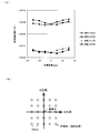
- FIG. 9A shows the measurement results of the volume resistivity in the film growth (straight plane) direction and the volume resistivity in the in-plane direction. From this figure, it can be seen that the volume resistivity differs by almost three orders of magnitude between the film growth direction and the in-plane direction.
- the horizontal axis in FIG. 9A indicates the measurement position on the surface of the ⁇ c-Si film 52. The measurement position is set to 0 mm with reference to a certain point. As shown in (b), it is a case where it is changed in the A direction and a case where it is changed in the B direction orthogonal thereto.
- the inventor of the present application has found a method for solving the above problem by changing the structure of the p layer and the n layer with respect to the conventional thin film solar cell.
- the thin film solar cell according to the present invention will be described.
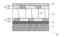
- FIG. 1 shows a schematic longitudinal sectional view of a first embodiment of the thin-film solar cell according to the present invention.
- the thin-film solar cell 10 of this example includes a metal electrode layer (first electrode layer) 12, a first semiconductor layer 13, a ⁇ c-Si layer (intrinsic semiconductor layer) 14, a second semiconductor layer 15, and a transparent electrode on a substrate 11.
- a (TCO) layer (second electrode layer) 16 is sequentially stacked.
- the first semiconductor layer 13 includes a plurality of n-type a-Si regions (n-type semiconductor regions) 131 that are formed to be spaced apart from each other in the in-plane direction, and between these n-type a-Si regions 131.
- the formed SiOx region (first insulator region) 132 is formed.
- the second semiconductor layer 15 is formed between a plurality of p-type a-Si regions (p-type semiconductor regions) 151 that are spaced apart from each other in the in-plane direction, and between these p-type a-Si regions 151.
- the SiOx region (second insulator region) 152 is formed.
- the n-type a-Si region 131 and the p-type a-Si region 151 are arranged so as not to overlap each other with the ⁇ c-Si layer 14 interposed therebetween, and further shown in FIG.
- regions (first insulator region 132 and second insulator region 152) made of SiOx as an insulating member are arranged at one or both ends of the grain boundary 30 formed in the ⁇ c-Si layer 14. It has a structure. By adopting such a structure, it is possible to prevent a short circuit of current between the n-type a-Si region 131 and the p-type a-Si region 151.
- the average value of the diameter (size) of the columnar crystals projected on the substrate surface (hereinafter referred to as “average column diameter”) for the actually produced ⁇ c-Si thin film was obtained, and based on this, the n-type a- The positions of the Si region 131 and the p-type a-Si region 151 are determined.
- the average column diameter of each columnar crystal in the ⁇ c-Si layer can be controlled by appropriately changing the film forming conditions.
- the average column diameter in the ⁇ c-Si layer 14 for a certain film forming condition is R
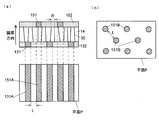
- the n-type a-Si region 131 and the p-type a-Si region 151 are projected on a plane P parallel to each layer. think of.
- the n-type a-Si region 131 and the p-type a-Si region 151 are arranged so as not to overlap each other with the ⁇ c-Si layer 14 interposed therebetween (upper view of FIG. 2A).
- the n-type a-Si region 131A and the p-type a-Si region 151A projected onto the plane P exist at positions separated from each other (the lower diagram in FIG. 2A).
- the n-type a-Si region 131 in the first semiconductor layer 13 and the first n-type a-Si region 131A in the first semiconductor layer 13 and the n-type a-Si region 131A in the first semiconductor layer 13 are arranged so that the distance L between the n-type a-Si region 131A and the p-type a-Si region 151A If the p-type a-Si region 151 in each of the two semiconductor layers 15 is disposed, the first insulator region 132 and the first insulator region 132 are formed at one or both ends of the crystal grain boundary 30 formed in the ⁇ c-Si layer 14.
- a structure in which the two-insulator region 152 is disposed can be employed.
- n-type a-Si region 131 and the p-type a-Si region 151 include an island-like shape (n-type a as shown in FIG. 2B) in addition to the strip shape shown in the lower diagram of FIG. -Si region 131B and p-type a-Si region 151B) can also be used.
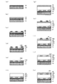
- a perturbation layer (not shown), a first electrode layer (metal thin film) 12, and a first semiconductor layer 13 made of only n-type a-Si are sequentially stacked on the substrate 11 (FIG. 3). (a) and (b)). Then, a resist pattern 40 is formed on the first semiconductor layer 13 (FIG. 3C), and an oxidation process using oxygen-containing plasma is performed. Thereby, the n-type a-Si region 131 and the SiOx region 132 are formed (FIG. 3D). Thereafter, the resist 40 is removed (FIG. 3E).
- a ⁇ c-Si layer 14 and a second semiconductor layer 15 made of only p-type a-Si are sequentially formed on the first semiconductor layer 13 (FIGS. 3 (f) and 3 (g)), and a resist is formed. 41 and oxidation treatment are performed to form a p-type a-Si region 151 and a SiOx region 152 in the second semiconductor layer 15 (FIGS. 3H and 3I). Thereafter, the resist 41 is removed (FIG. 3 (j)), and the transparent electrode (TCO) layer 16 is formed (FIG. 3 (k)). Thereby, the thin film solar cell 10 of a present Example is manufactured.
- FIG. 4 is a schematic longitudinal sectional view of the thin film solar cell of the second embodiment in which the thin film solar cell having the structure of the first embodiment is applied to a pn junction.
- This example is a pn junction type thin film solar cell in which an n-type ⁇ c-Si layer 63 and a p-type ⁇ c-Si layer 65 are in contact with each other, and the concept of the present invention is applied to two electrode layers sandwiching them.
- the first electrode layer 62 of the present embodiment is composed of a plurality of metal electrode regions 621 that are formed apart from each other in the in-plane direction, and a first insulator region 622 formed between these regions.
- the second electrode layer 66 includes a plurality of transparent electrode regions 661 that are formed to be spaced apart from each other in the in-plane direction, and a second insulator region 662 that is formed between these regions.
- the metal electrode region 621 and the transparent electrode region 661 that are closest to each other on the surface projected onto the substrate 61 are arranged such that the distance between them is equal to or greater than the average column diameter of the n-type ⁇ c-Si layer 63 and the p-type ⁇ c-Si layer 65. To do.
- a light emitting diode has a structure in which a lower electrode, an n-type cladding layer, an active layer (intermediate semiconductor layer), a p-type cladding layer, and an upper electrode are sequentially stacked on a substrate.
- a lower electrode an n-type cladding layer, an active layer (intermediate semiconductor layer), a p-type cladding layer, and an upper electrode are sequentially stacked on a substrate.
- single crystals such as InGaN have been used for the active layer.
- a microcrystalline semiconductor has been made of a single crystal semiconductor. It is being used instead.
- the same problem as that of a solar cell occurs. Therefore, by using the same structure as the first semiconductor layer and the second semiconductor layer for the n-type cladding layer and the p-type cladding layer, The light emission efficiency of the light emitting diode can be increased.
- the layer having a columnar structure is a microcrystalline semiconductor
- the present invention is not limited to this.
- the present invention can be applied in the same manner as in the above embodiments as long as it is a semiconductor having a columnar structure.
- p-type a-Si layer 30 ... Grain boundary 31 ... Photoexcited carrier 31A ... Electron 31B ... Hole 32 ... Current flow direction 33 ... Leakage current (reverse direction) Saturation current) direction 40, 41 ... resist (resist pattern) 50 ... Glass substrate 51 ... Tungsten film 52 ... ⁇ c-Si film 53 ... Aluminum film 61 ... Substrate 62 ... First electrode layer 621 ... Metal electrode region 622 ... First insulator region 63 ... n-type ⁇ c-Si layer 65 ... p Type ⁇ c-Si layer 66 ... second electrode layer 661 ... transparent electrode region 662 ... second insulator region
Landscapes
- Photovoltaic Devices (AREA)
Abstract
柱状構造を有する半導体薄膜を用いた薄膜太陽電池において、リーク電流を抑制することができる薄膜太陽電池を提供する。本発明に係る薄膜太陽電池10では、n型a-Si領域131とp型a-Si領域151とが、μc-Si層14を挟んで互いに重なり合わないように、各層に平行な平面において所定の距離をおいて配置される構造を有している。これにより、μc-Si層14内で柱状晶間に形成される結晶粒界30の一方もしくは両方の端部に絶縁部材であるSiOxから成る層(第1絶縁層132及び第2絶縁層152)が配置されるため、n型a-Si層131とp型a-Si層151との間で結晶粒界30を介して電流が短絡することを防ぐことができる。
Description
本発明は、薄膜太陽電池及び該薄膜太陽電池と同じ構造を有する半導体デバイスに関する。
近年、温暖化等の環境問題の観点から、二酸化炭素を排出しないクリーンなエネルギー源として太陽電池が注目されている。太陽電池には様々な種類・形態のものがあるが、光エネルギーを電力に変換する光電変換効率の高い太陽電池として、高純度のシリコン単結晶を用いた単結晶シリコン太陽電池がよく知られている。
単結晶シリコン太陽電池では、p型ドーパントをドープしたp層とn型ドーパントをドープしたn層とが互いに接するpn接合と呼ばれる構造が一般的に用いられる。また、p層とn層にはそれぞれ電極が取り付けられている。
p型半導体とn型半導体を接合した場合、n型半導体側の電子は、電子密度の低いp型半導体領域に拡散し、同様に正孔についてはその逆が生じる。こうしたキャリアの移動は熱平衡状態が保たれるまで続き、その結果、pn接合界面付近ではn領域中の電子が不足して正に帯電した空間電荷が現れ、p側ではその逆に負に帯電した空間電荷が生じて、接合前のフェルミ準位の差に相当するエネルギーの電位障壁が誘起される。その電位差はpn接合の拡散電位と呼ばれ、拡散電位の存在する領域はpからnへの遷移領域と呼ばれる。この遷移領域のキャリア密度はバルクよりも少ないため、空乏層とも呼ばれる。空乏層に入射した光のエネルギーにより空乏層でキャリアが生成されると、拡散電位により形成される電界によって電子がn層に、正孔がp層に移動する。これらの光励起キャリアが両層に取り付けられた電極により外部に取り出されることで、太陽電池として動作する。このように、pn接合では空乏層が発電層(光電変換層)として働くことになる。
単結晶シリコン太陽電池は上記のように光電変換効率に優れている。しかしながら、半導体基板として高純度シリコン単結晶を用いるため、生産コストが高くなってしまうという問題がある。また、シリコン単結晶の基板はインゴットをスライスして製造されるため、薄膜化・大面積化が容易でない。
薄膜化や大面積化、低コスト化といった諸問題を解決する太陽電池として、アモルファス(非晶質)シリコン太陽電池が実用化されている。アモルファスシリコン太陽電池では、pn接合における空乏層に相当する層を予め設けたpin接合と呼ばれる構造が一般的に用いられる。このpin接合では、p層とn層の間に挟まれたノンドープの真性半導体層(i層)が発電層として機能する。
アモルファスシリコン太陽電池は、光電変換効率は単結晶シリコン太陽電池に比べて低いものの、化学的気相成長法(CVD法)などを用いて製造することができるため、薄膜化・大面積化が容易である。また、原料の使用量を削減でき、低コストで製造することができるといった利点もある。しかしながら、アモルファスシリコン太陽電池は太陽光スペクトルに対する光吸収特性が狭く、さらに光の入射によって光電変換効率が低下する(Stabler-Wronski効果)という光劣化の問題があるため、長期間に亘って安定した電力を供給することが困難であった。
これらの光吸収特性や光劣化といった問題を解決するため、近年ではナノメートルからマイクロメートルサイズのシリコン微結晶で構成された薄膜をi層に用いた微結晶シリコン太陽電池が開発されている。微結晶シリコンはアモルファスシリコンと同様にプラズマCVD法を用いて製造することができるため、薄膜化や大面積化、低コスト化が容易であると共に、構成成分が結晶質であるため、上記の光吸収特性や光劣化の問題を改善することができる。さらに、光励起キャリアの移動度がアモルファスシリコンに比べて大きいという特長も有している。
"アモルファスシリコン/薄膜結晶シリコン積層型太陽電池",[online],三洋電機株式会社,[平成21年12月14日検索],インターネット<URL:http://sanyo.com/technical_review/jp/no75/pdf/7504.pdf>
これらの特長を有しているにも関わらず、現在製造されている微結晶シリコン太陽電池の光電変換効率はアモルファスシリコン太陽電池と同程度に過ぎない。微結晶シリコン太陽電池の光電変換効率が低い要因は幾つか考えられるが、その一つとして、微結晶シリコン薄膜内に形成される結晶粒界においてリーク電流が発生することが挙げられる(非特許文献1)。
例えばpin接合の太陽電池では、光励起キャリアを効率良く移動させるために、発電層であるi層のp層側の面とn層側の面の間に電荷分離を効率良く行うのに十分な電位差が生じることが重要となる。従って、i層はその電位差を維持するための膜抵抗を有する必要がある。
しかしながら、微結晶シリコン薄膜では製膜の過程で、結晶粒子が膜成長方向に柱状に成長し、その結果、これらの柱状晶の間に同じ方向に延びる結晶粒界が形成される。このような柱状晶が多数並んだ構造(以下、「柱状構造」とする)では柱状晶間の結晶粒界において電流のリークが生じやすく、膜成長方向の電位差を維持することが困難となるため、光電変換効率が低下してしまう可能性がある。
本発明が解決しようとする課題は、柱状構造を有する薄膜太陽電池において、リーク電流を抑制することができる薄膜太陽電池を提供することである。また、同様の結晶構造を有する発光ダイオード等の半導体デバイスに対して、リーク電流による性能低下を抑制することができる半導体デバイスを提供することである。
上記課題を解決するために成された本発明に係る薄膜太陽電池は、
第1電極層、第1半導体層、真性半導体層、第2半導体層、第2電極層が順に積層された構造を有する薄膜太陽電池において、
前記第1半導体層が、面内方向に互いに離間して形成された複数のn型半導体領域と、これらのn型半導体領域の間に形成された第1絶縁体領域と、から成り、
前記真性半導体層が、積層方向に延びる柱状晶が並ぶ柱状構造を有し、
前記第2半導体層が、面内方向に互いに離間して形成された複数のp型半導体領域と、これらのp型半導体領域の間に形成された第2絶縁体領域と、から成り、
各層に平行な平面上に前記p型半導体領域及び前記n型半導体領域を射影した際、一つのp型半導体領域と該p型半導体領域に最近接のn型半導体領域との間の距離が、前記真性半導体層の柱状晶の前記平面上における径の平均値以上である
ことを特徴とする。
第1電極層、第1半導体層、真性半導体層、第2半導体層、第2電極層が順に積層された構造を有する薄膜太陽電池において、
前記第1半導体層が、面内方向に互いに離間して形成された複数のn型半導体領域と、これらのn型半導体領域の間に形成された第1絶縁体領域と、から成り、
前記真性半導体層が、積層方向に延びる柱状晶が並ぶ柱状構造を有し、
前記第2半導体層が、面内方向に互いに離間して形成された複数のp型半導体領域と、これらのp型半導体領域の間に形成された第2絶縁体領域と、から成り、
各層に平行な平面上に前記p型半導体領域及び前記n型半導体領域を射影した際、一つのp型半導体領域と該p型半導体領域に最近接のn型半導体領域との間の距離が、前記真性半導体層の柱状晶の前記平面上における径の平均値以上である
ことを特徴とする。
なお、本発明における柱状晶とは、下層から上層までを貫く単一の結晶粒子のことである。このため、隣接する柱状晶間において上層と下層を繋ぐように結晶粒界が形成される。また、本発明における2つの領域間の「距離」とは、その射影平面内での2つの領域の間の長さが最小となる値のことである。
また、上記課題を解決するために成された本発明に係る半導体デバイスは、
第1電極層、第1半導体層、中間半導体層、第2半導体層、第2電極層が順に積層された構造を有する半導体デバイスにおいて、
前記第1半導体層が、面内方向に互いに離間して形成された複数のn型半導体領域と、これらのn型半導体領域の間に形成された第1絶縁体領域と、から成り、
前記中間半導体層が、積層方向に延びる柱状晶が並ぶ柱状構造を有し、
前記第2半導体層が、面内方向に互いに離間して形成された複数のp型半導体領域と、これらのp型半導体領域の間に形成された第2絶縁体領域と、から成り、
各層に平行な平面上に前記p型半導体領域及び前記n型半導体領域を射影した際、一つのp型半導体領域と該p型半導体領域に最近接のn型半導体領域との間の距離が、前記中間半導体層の柱状晶の前記平面上における径の平均値以上である
ことを特徴とする。
第1電極層、第1半導体層、中間半導体層、第2半導体層、第2電極層が順に積層された構造を有する半導体デバイスにおいて、
前記第1半導体層が、面内方向に互いに離間して形成された複数のn型半導体領域と、これらのn型半導体領域の間に形成された第1絶縁体領域と、から成り、
前記中間半導体層が、積層方向に延びる柱状晶が並ぶ柱状構造を有し、
前記第2半導体層が、面内方向に互いに離間して形成された複数のp型半導体領域と、これらのp型半導体領域の間に形成された第2絶縁体領域と、から成り、
各層に平行な平面上に前記p型半導体領域及び前記n型半導体領域を射影した際、一つのp型半導体領域と該p型半導体領域に最近接のn型半導体領域との間の距離が、前記中間半導体層の柱状晶の前記平面上における径の平均値以上である
ことを特徴とする。
本発明に係る薄膜太陽電池は、第1半導体層と第2半導体層の一部に絶縁体領域を設け、真性半導体層の柱状晶の間に形成される膜成長方向に延びる結晶粒界の一方もしくは両方の端部において、該絶縁体領域が配置される構造としている。これにより、膜成長方向の結晶粒界で電流がリークすることを防ぐことができるため、真性半導体層の第1半導体層側の面と第2半導体層側の面の間の電位差を維持することができ、薄膜太陽電池の光電変換効率を高めることが可能となる。
また、本発明に係る薄膜太陽電池の構造は、柱状構造の半導体層を備える他の半導体デバイスにも用いることができる。例えば、フォトダイオードは太陽電池と構造や機能が同じであるため、本発明の構造の薄膜太陽電池はフォトダイオードにそのまま適用することができる。レーザダイオードや発光ダイオードなどの半導体光デバイスにおいても、太陽電池との違いは、光を電気に変換するか、電気を光に変換するかの機能面での差だけであって、構造自体は太陽電池と同じである。従って、本発明の構造の半導体デバイスは太陽電池以外の用途にも好適に用いることができ、半導体デバイスの機能向上に貢献することができる。
まず、従来のpin接合型の薄膜太陽電池について、図5~7を用いて概略的に説明する。
図5はpin接合型の薄膜太陽電池の一般的な構造を示す概略縦断面図である。この薄膜太陽電池20は、基板21上に金属電極層22、n型アモルファスシリコン(a-Si)層23、微結晶シリコン(μc-Si)層24、p型a-Si層25、透明電極層26が順に積層された構造を有している。この構造の薄膜太陽電池では、n型a-Si層23及びp型a-Si層25がそれぞれn層及びp層に対応し、μc-Si層24がi層に対応する。
図5はpin接合型の薄膜太陽電池の一般的な構造を示す概略縦断面図である。この薄膜太陽電池20は、基板21上に金属電極層22、n型アモルファスシリコン(a-Si)層23、微結晶シリコン(μc-Si)層24、p型a-Si層25、透明電極層26が順に積層された構造を有している。この構造の薄膜太陽電池では、n型a-Si層23及びp型a-Si層25がそれぞれn層及びp層に対応し、μc-Si層24がi層に対応する。
図5の薄膜太陽電池20は、例えばプラズマCVD法により製造することができる。そのため、高純度のシリコン単結晶(c-Si)を用いるc-Si太陽電池よりも低コストで製造することができ、かつ大面積化や薄膜化を容易に行うことができる。また発電層としてμc-Siを用いているため、a-Si太陽電池で問題となっていた光劣化を抑制することができる。
しかしながら、μc-Siには柱状構造に由来する結晶粒界が形成されるという問題がある。図6のμc-Si薄膜の断面TEM像には、μc-Siに結晶粒界(図中の白い筋)が形成され、膜成長方向に延びていることが示されている。薄膜太陽電池20の構造では、この結晶粒界30においてリーク電流が流れることにより性能が低下する。これを図7を用いて説明する。
図7に示すように、pin構造の薄膜太陽電池20では、光の入射によってi層であるμc-Si層24において光励起キャリア(電子正孔対)31が生成される。この光励起キャリア31のうち、電子31Aはn型a-Si層23に、正孔31Bはp型a-Si層25に、μc-Si層24のp型a-Si層23側の面とn型a-Si層25側の面の間の電位差(電圧)により形成された電界によって移動する。このときμc-Si層24にかかる電圧が低ければ、電荷(電子と正孔)が十分に分離されず、再結合してしまい、光電変換効率が低下する。
従って、μc-Si層24にかかる電圧は高ければ高い方が良い。しかしながら、μc-Si層24には、図6に示すように膜成長方向に延びる結晶粒界30が形成されているため、電圧が高くなると、電流の流れる方向32とは逆方向に、結晶粒界30を通じてリーク電流(逆方向飽和電流)33が流れてしまう。これにより、μc-Siなどの微結晶半導体をi層に用いた薄膜太陽電池ではあまり電圧が高くならず、電荷分離が十分に行われないため、光電変換効率が低下するものと考えられる。
光励起キャリアを効率良く移動させるには、発電層であるμc-Si層24のn型a-Si層23側の面とp型a-Si層25側の面の間に十分な電位差を得る必要があり、そのためにはμc-Si層24が高い膜抵抗を有する必要がある。上記したようにμc-Si層24の膜抵抗の低下が結晶粒界30により生じるとすると、膜成長方向に電圧を印加した場合と面内方向に電圧を印加した場合とでは、μc-Si層24の抵抗率が異なると本願発明者は予測した。
この予測を実証するため、本願発明者は以下に示す実験を行った。
まず、膜成長方向の抵抗率を測定するために、図8(a)に示す構造の半導体デバイスを作成した。この半導体デバイスは、厚さ4インチのガラス基板50上に、下部電極として厚さ200nmのタングステン膜51をスパッタリング法にて形成した後、基板温度を300℃にしてプラズマCVD法により厚さ2μmのμc-Si(微結晶シリコン)膜52を形成した。μc-Si膜52上には、上部電極として直径1mm、厚さ500nmのアルミニウム膜53を蒸着マスクを用いながら真空蒸着法により形成した。そして、タングステン膜51とアルミニウム膜53との間に直流電圧を印加して、μc-Si膜52の膜成長方向の抵抗を測定した。この測定値とμc-Si膜の厚さ2μmとの積により、膜成長方向の体積抵抗率を算出した。
まず、膜成長方向の抵抗率を測定するために、図8(a)に示す構造の半導体デバイスを作成した。この半導体デバイスは、厚さ4インチのガラス基板50上に、下部電極として厚さ200nmのタングステン膜51をスパッタリング法にて形成した後、基板温度を300℃にしてプラズマCVD法により厚さ2μmのμc-Si(微結晶シリコン)膜52を形成した。μc-Si膜52上には、上部電極として直径1mm、厚さ500nmのアルミニウム膜53を蒸着マスクを用いながら真空蒸着法により形成した。そして、タングステン膜51とアルミニウム膜53との間に直流電圧を印加して、μc-Si膜52の膜成長方向の抵抗を測定した。この測定値とμc-Si膜の厚さ2μmとの積により、膜成長方向の体積抵抗率を算出した。
また、面内方向の抵抗率の測定には、図8(b)に示す構造の半導体デバイスを使用した。この半導体デバイスは、厚さ4インチのガラス基板50上に、基板温度を300℃にしてプラズマCVD法により厚さ2μmのμc-Si膜52を形成した。そして、四端子法によりμc-Si膜52の表面抵抗率を測定値し、この表面抵抗率の測定値とμc-Si膜の厚さ2μmとの積により面内方向の体積抵抗率を算出した。
膜成長(面直)方向の体積抵抗率と面内方向の体積抵抗率の測定結果を図9(a)に示す。この図から、膜成長方向と面内方向とでは体積抵抗率が3桁近くも異なっていることが分かる。なお、図9(a)の横軸はμc-Si膜52上の面内での測定位置を示しており、或る点を基準にしてその計測位置を0mmとし、そこから測定位置を図9(b)に示すようにA方向に変化させた場合とそれと直交するB方向に変化させた場合のものである。
これらの実験結果を基に、本願発明者は、従来の薄膜太陽電池に対してp層とn層の構造を変えることにより、上記の問題を解決する方法を見出した。以下、本発明に係る薄膜太陽電池について説明を行う。
本発明に係る薄膜太陽電池の第1実施例の概略縦断面図を図1に示す。
本実施例の薄膜太陽電池10は、基板11上に金属電極層(第1電極層)12、第1半導体層13、μc-Si層(真性半導体層)14、第2半導体層15、透明電極(TCO)層(第2電極層)16、が順に積層された構造を有している。ここで、第1半導体層13は、面内方向に互いに離間して形成された複数のn型a-Si領域(n型半導体領域)131と、これらのn型a-Si領域131の間に形成されたSiOx領域(第1絶縁体領域)132から成る。また、第2半導体層15は、面内方向に互いに離間して形成された複数のp型a-Si領域(p型半導体領域)151と、これらのp型a-Si領域151の間に形成されたSiOx領域(第2絶縁体領域)152から成る。
本実施例の薄膜太陽電池10は、基板11上に金属電極層(第1電極層)12、第1半導体層13、μc-Si層(真性半導体層)14、第2半導体層15、透明電極(TCO)層(第2電極層)16、が順に積層された構造を有している。ここで、第1半導体層13は、面内方向に互いに離間して形成された複数のn型a-Si領域(n型半導体領域)131と、これらのn型a-Si領域131の間に形成されたSiOx領域(第1絶縁体領域)132から成る。また、第2半導体層15は、面内方向に互いに離間して形成された複数のp型a-Si領域(p型半導体領域)151と、これらのp型a-Si領域151の間に形成されたSiOx領域(第2絶縁体領域)152から成る。
本実施例の薄膜太陽電池10では、n型a-Si領域131とp型a-Si領域151とが、μc-Si層14を挟んで互いに重なり合わないように配置され、さらに図1に示すように、μc-Si層14に形成される結晶粒界30の一方もしくは両方の端部に絶縁部材であるSiOxから成る領域(第1絶縁体領域132及び第2絶縁体領域152)が配置される構造を有する。このような構造を採ることにより、n型a-Si領域131とp型a-Si領域151との間で電流の短絡が生じることを防ぐことができる。
しかしながら、結晶粒界30がμc-Si層14のどこに形成されるかを事前に知ることは困難である。従って、実際に作製したμc-Si薄膜について、基板面に射影した柱状晶の径(大きさ)の平均値(以下、「平均柱径」とする)を求め、これを基にn型a-Si領域131とp型a-Si領域151の位置を決定する。
μc-Si層内の各柱状晶の平均柱径は、製膜条件を適宜変更することで制御することができる。ここで、ある製膜条件に対するμc-Si層14内の平均柱径をRとし、各層に平行な平面P上に、n型a-Si領域131とp型a-Si領域151を射影した場合を考える。上記のように、n型a-Si領域131とp型a-Si領域151はμc-Si層14を挟んで互いに重なり合わないように配置されているため(図2(a)の上図)、平面P上に射影したn型a-Si領域131A及びp型a-Si領域151Aは、互いに離間した位置に存在する(図2(a)の下図)。この平面P上で最近接するn型a-Si領域131Aとp型a-Si領域151Aの距離LがL≧Rとなるように、第1半導体層13内のn型a-Si領域131と第2半導体層15内のp型a-Si領域151がそれぞれ配置されていれば、μc-Si層14に形成される結晶粒界30の一方もしくは両方の端部に第1絶縁体領域132及び第2絶縁体領域152が配置される構造とすることができる。
なお、n型a-Si領域131及びp型a-Si領域151には、図2(a)の下図に示した帯状の他、図2(b)のように島状の形状(n型a-Si領域131B及びp型a-Si領域151B)のものも用いることができる。
次に、プラズマCVD法を用いた薄膜太陽電池10の製造手順について、図3を参照して説明する。
まず、基板11上に、パータベーション層(図示せず)と、第1電極層(金属薄膜)12と、n型a-Siのみから成る第1半導体層13と、を順に積層する(図3(a)及び(b))。そして、第1半導体層13の上にレジストパターン40を形成し(図3(c))、酸素含有プラズマによる酸化処理を施す。これにより、n型a-Si領域131及びSiOx領域132が形成される(図3(d))。その後、レジスト40を除去する(図3(e))。
まず、基板11上に、パータベーション層(図示せず)と、第1電極層(金属薄膜)12と、n型a-Siのみから成る第1半導体層13と、を順に積層する(図3(a)及び(b))。そして、第1半導体層13の上にレジストパターン40を形成し(図3(c))、酸素含有プラズマによる酸化処理を施す。これにより、n型a-Si領域131及びSiOx領域132が形成される(図3(d))。その後、レジスト40を除去する(図3(e))。
次に、第1半導体層13の上に、μc-Si層14と、p型a-Siのみから成る第2半導体層15とを順に形成し(図3(f)及び(g))、レジスト41と酸化処理により第2半導体層15内にp型a-Si領域151及びSiOx領域152を形成する(図3(h)及び(i))。その後、レジスト41を除去し(図3(j))、透明電極(TCO)層16を形成する(図3(k))。これにより、本実施例の薄膜太陽電池10が製造される。
第1実施例に示したpin接合の薄膜太陽電池の構造は、pn接合の薄膜太陽電池に対しても応用することができる。図4に、第1実施例の構造の薄膜太陽電池をpn接合に応用した、第2実施例の薄膜太陽電池の概略縦断面図を示す。
本実施例は、n型のμc-Si層63とp型のμc-Si層65とが互いに接するpn接合型の薄膜太陽電池であり、これらを挟持する2つの電極層に本発明の概念を用いている。すなわち、本実施例の第1電極層62は、面内方向に互いに離間して形成された複数の金属電極領域621と、これらの領域の間に形成された第1絶縁体領域622から成り、第2電極層66は、面内方向に互いに離間して形成された複数の透明電極領域661と、これらの領域の間に形成された第2絶縁体領域662とから成る。また、基板61に射影した面上で最近接する金属電極領域621と透明電極領域661の距離が、n型μc-Si層63及びp型μc-Si層65の平均柱径以上となるように配置する。
このような構造を採ることにより、pn接合の薄膜太陽電池であっても、第1実施例と同様の効果を奏することができる。
なお、各実施例に示した薄膜太陽電池の構造は、フォトダイオードや発光ダイオードなど、他の半導体デバイスにも応用することができる。例えば、発光ダイオードでは、基板上に下部電極、n型クラッド層、活性層(中間半導体層)、p型クラッド層、上部電極が順に積層された構造を有している。従来、活性層には例えばInGaN等の単結晶が用いられていたが、太陽電池と同様に単結晶半導体では高コスト且つ大面積化が困難であるため、近年では微結晶半導体が単結晶半導体の代わりに用いられつつある。しかしながら、微結晶半導体を用いた場合でも、太陽電池と同様の問題が生じるため、n型クラッド層とp型クラッド層に上記の第1半導体層及び第2半導体層と同じ構造を用いることにより、発光ダイオードの発光効率を高めることができる。
また、上記各実施例では、柱状構造を有する層が微結晶半導体である場合を例に説明したが、本発明はこれに限定されない。例えば多結晶半導体のように結晶の粒径が大きくても、柱状構造を有する半導体であれば、上記各実施例と同様に本発明を適用することができる。
10、20…薄膜太陽電池
11、21…基板
13…第1半導体層
131、131A、131B…n型a-Si領域(n型半導体領域)
132…SiOx領域(第1絶縁体領域)
14、24…μc-Si層(真性半導体層)
15…第2半導体層
151、151A、151B…p型a-Si領域(p型半導体領域)
152…SiOx領域(第2絶縁体領域)
16、26…透明電極層(第2電極層)
22…金属電極層
23…n型a-Si層
25…p型a-Si層
30…結晶粒界
31…光励起キャリア
31A…電子
31B…正孔
32…電流の流れる方向
33…リーク電流(逆方向飽和電流)の流れる方向
40、41…レジスト(レジストパターン)
50…ガラス基板
51…タングステン膜
52…μc-Si膜
53…アルミニウム膜
61…基板
62…第1電極層
621…金属電極領域
622…第1絶縁体領域
63…n型μc-Si層
65…p型μc-Si層
66…第2電極層
661…透明電極領域
662…第2絶縁体領域
11、21…基板
13…第1半導体層
131、131A、131B…n型a-Si領域(n型半導体領域)
132…SiOx領域(第1絶縁体領域)
14、24…μc-Si層(真性半導体層)
15…第2半導体層
151、151A、151B…p型a-Si領域(p型半導体領域)
152…SiOx領域(第2絶縁体領域)
16、26…透明電極層(第2電極層)
22…金属電極層
23…n型a-Si層
25…p型a-Si層
30…結晶粒界
31…光励起キャリア
31A…電子
31B…正孔
32…電流の流れる方向
33…リーク電流(逆方向飽和電流)の流れる方向
40、41…レジスト(レジストパターン)
50…ガラス基板
51…タングステン膜
52…μc-Si膜
53…アルミニウム膜
61…基板
62…第1電極層
621…金属電極領域
622…第1絶縁体領域
63…n型μc-Si層
65…p型μc-Si層
66…第2電極層
661…透明電極領域
662…第2絶縁体領域
Claims (6)
- 第1電極層、第1半導体層、真性半導体層、第2半導体層、第2電極層が順に積層された構造を有する薄膜太陽電池において、
前記第1半導体層が、面内方向に互いに離間して形成された複数のn型半導体領域と、これらのn型半導体領域の間に形成された第1絶縁体領域と、から成り、
前記真性半導体層が、積層方向に延びる柱状晶が並ぶ柱状構造を有し、
前記第2半導体層が、面内方向に互いに離間して形成された複数のp型半導体領域と、これらのp型半導体領域の間に形成された第2絶縁体領域と、から成り、
各層に平行な平面上に前記p型半導体領域及び前記n型半導体領域を射影した際、一つのp型半導体領域と該p型半導体領域に最近接のn型半導体領域との間の距離が、前記真性半導体層の柱状晶の前記平面上における径の平均値以上である
ことを特徴とする薄膜太陽電池。 - 前記p型半導体領域及び/又はn型半導体領域が、アモルファス半導体から成ることを特徴とする請求項1に記載の薄膜太陽電池。
- 第1電極層、p型半導体層、n型半導体層、第2電極層が順に積層された構造を有する薄膜太陽電池において、
前記第1電極層が、面内方向に互いに離間して形成された複数の第1電極領域と、これらの第1電極領域の間に形成された第1絶縁体領域と、から成り、
前記p型半導体層及び前記n型半導体層が、積層方向に延びる柱状晶が並ぶ柱状構造を有し、
前記第2電極層が、面内方向に互いに離間して形成された複数の第2電極領域と、これらの第2電極領域の間に形成された第2絶縁体領域と、から成り、
各層に平行な平面上に前記第1電極領域及び前記2電極領域を射影した際、一つの第1電極領域と該第1電極領域に最近接の第2電極領域との間の距離が、前記第1半導体層の柱状晶の前記平面上における径の平均値以上である
ことを特徴とする薄膜太陽電池。 - 第1電極層、第1半導体層、中間半導体層、第2半導体層、第2電極層が順に積層された構造を有する半導体デバイスにおいて、
前記第1半導体層が、面内方向に互いに離間して形成された複数のn型半導体領域と、これらのn型半導体領域の間に形成された第1絶縁体領域と、から成り、
前記中間半導体層が、積層方向に延びる柱状晶が並ぶ柱状構造を有し、
前記第2半導体層が、面内方向に互いに離間して形成された複数のp型半導体領域と、これらのp型半導体領域の間に形成された第2絶縁体領域と、から成り、
各層に平行な平面上に前記p型半導体領域及び前記n型半導体領域を射影した際、一つのp型半導体領域と該p型半導体領域に最近接のn型半導体領域との間の距離が、前記中間半導体層の柱状晶の前記平面上における径の平均値以上である
ことを特徴とする半導体デバイス。 - 前記p型半導体領域及び/又はn型半導体領域が、アモルファス半導体から成ることを特徴とする請求項4に記載の半導体デバイス。
- 第1電極層、p型半導体層、n型半導体層、第2電極層が順に積層された構造を有する半導体デバイスにおいて、
前記第1電極層が、面内方向に互いに離間して形成された複数の第1電極領域と、これらの第1電極領域の間に形成された第1絶縁体領域と、から成り、
前記p型半導体層及び前記n型半導体層が、積層方向に延びる柱状晶が並ぶ柱状構造を有し、
前記第2電極層が、面内方向に互いに離間して形成された複数の第2電極領域と、これらの第2電極領域の間に形成された第2絶縁体領域と、から成り、
各層に平行な平面上に前記第1電極領域及び前記2電極領域を射影した際、一つの第1電極領域と該第1電極領域に最近接の第2電極領域との間の距離が、前記第1半導体層の柱状晶の前記平面上における径の平均値以上である
ことを特徴とする半導体デバイス。
Applications Claiming Priority (2)
| Application Number | Priority Date | Filing Date | Title |
|---|---|---|---|
| JP2010-173508 | 2010-08-02 | ||
| JP2010173508A JP2012033804A (ja) | 2010-08-02 | 2010-08-02 | 薄膜太陽電池及び半導体デバイス |
Publications (1)
| Publication Number | Publication Date |
|---|---|
| WO2012018023A1 true WO2012018023A1 (ja) | 2012-02-09 |
Family
ID=45559520
Family Applications (1)
| Application Number | Title | Priority Date | Filing Date |
|---|---|---|---|
| PCT/JP2011/067697 Ceased WO2012018023A1 (ja) | 2010-08-02 | 2011-08-02 | 薄膜太陽電池及び半導体デバイス |
Country Status (3)
| Country | Link |
|---|---|
| JP (1) | JP2012033804A (ja) |
| TW (1) | TW201220514A (ja) |
| WO (1) | WO2012018023A1 (ja) |
Families Citing this family (1)
| Publication number | Priority date | Publication date | Assignee | Title |
|---|---|---|---|---|
| EP3998653B1 (en) * | 2019-07-24 | 2024-10-23 | National Institute of Advanced Industrial Science And Technology | Electrode having columnar structure provided with multilayer part |
Citations (1)
| Publication number | Priority date | Publication date | Assignee | Title |
|---|---|---|---|---|
| JP2004134432A (ja) * | 2002-10-08 | 2004-04-30 | Sanyo Electric Co Ltd | 光電変換装置 |
-
2010
- 2010-08-02 JP JP2010173508A patent/JP2012033804A/ja active Pending
-
2011
- 2011-08-02 WO PCT/JP2011/067697 patent/WO2012018023A1/ja not_active Ceased
- 2011-08-02 TW TW100127332A patent/TW201220514A/zh unknown
Patent Citations (1)
| Publication number | Priority date | Publication date | Assignee | Title |
|---|---|---|---|---|
| JP2004134432A (ja) * | 2002-10-08 | 2004-04-30 | Sanyo Electric Co Ltd | 光電変換装置 |
Also Published As
| Publication number | Publication date |
|---|---|
| JP2012033804A (ja) | 2012-02-16 |
| TW201220514A (en) | 2012-05-16 |
Similar Documents
| Publication | Publication Date | Title |
|---|---|---|
| US10707367B2 (en) | Contact for silicon heterojunction solar cells | |
| US10903375B2 (en) | Solar cell | |
| KR100850641B1 (ko) | 고효율 결정질 실리콘 태양전지 및 그 제조방법 | |
| TW201001726A (en) | Techniques for enhancing efficiency of photovoltaic devices using high-aspect-ratio nanostructures | |
| CN102290485A (zh) | 制造薄膜太阳能电池的方法 | |
| JP2014207310A (ja) | 太陽電池セル | |
| KR20110100725A (ko) | 태양전지 및 그 제조방법 | |
| JP2010283406A (ja) | 太陽電池 | |
| JP2013524501A (ja) | Pn接合およびショットキー接合を有する多重太陽電池およびその製造方法 | |
| JP5390013B2 (ja) | 光発電素子および多接合薄膜太陽電池 | |
| US8697986B2 (en) | Photovoltaic device with double-junction | |
| JP2012033804A (ja) | 薄膜太陽電池及び半導体デバイス | |
| Hekmatshoar et al. | Novel heterojunction solar cells with conversion efficiencies approaching 21% on p-type crystalline silicon substrates | |
| CN103594552B (zh) | 一种光伏电池的制造方法 | |
| KR101652402B1 (ko) | 나노와이어 구조의 태양전지 및 제조방법 | |
| US20120318337A1 (en) | Solar Cell | |
| KR20130104347A (ko) | 태양 전지 및 그 제조 방법 | |
| KR101437070B1 (ko) | 광기전력 소자 | |
| KR101961370B1 (ko) | 태양 전지 | |
| KR20120014835A (ko) | 박막형 태양전지 모듈 및 그의 제조방법 | |
| KR101562265B1 (ko) | 박막 태양전지 및 그 제조방법 | |
| KR20120067544A (ko) | 박막 태양전지 및 이의 제조 방법 | |
| KR101854237B1 (ko) | 태양전지 및 그 제조방법 | |
| JP6333139B2 (ja) | 光電変換素子および光電変換素子の製造方法 | |
| JP2010267831A (ja) | 半導体装置 |
Legal Events
| Date | Code | Title | Description |
|---|---|---|---|
| 121 | Ep: the epo has been informed by wipo that ep was designated in this application |
Ref document number: 11814648 Country of ref document: EP Kind code of ref document: A1 |
|
| NENP | Non-entry into the national phase |
Ref country code: DE |
|
| 122 | Ep: pct application non-entry in european phase |
Ref document number: 11814648 Country of ref document: EP Kind code of ref document: A1 |