WO2012017863A1 - 液晶表示装置 - Google Patents
液晶表示装置 Download PDFInfo
- Publication number
- WO2012017863A1 WO2012017863A1 PCT/JP2011/066973 JP2011066973W WO2012017863A1 WO 2012017863 A1 WO2012017863 A1 WO 2012017863A1 JP 2011066973 W JP2011066973 W JP 2011066973W WO 2012017863 A1 WO2012017863 A1 WO 2012017863A1
- Authority
- WO
- WIPO (PCT)
- Prior art keywords
- liquid crystal
- electrode
- display device
- crystal display
- protrusion
- Prior art date
- Legal status (The legal status is an assumption and is not a legal conclusion. Google has not performed a legal analysis and makes no representation as to the accuracy of the status listed.)
- Ceased
Links
Images







Classifications
-
- G—PHYSICS
- G02—OPTICS
- G02F—OPTICAL DEVICES OR ARRANGEMENTS FOR THE CONTROL OF LIGHT BY MODIFICATION OF THE OPTICAL PROPERTIES OF THE MEDIA OF THE ELEMENTS INVOLVED THEREIN; NON-LINEAR OPTICS; FREQUENCY-CHANGING OF LIGHT; OPTICAL LOGIC ELEMENTS; OPTICAL ANALOGUE/DIGITAL CONVERTERS
- G02F1/00—Devices or arrangements for the control of the intensity, colour, phase, polarisation or direction of light arriving from an independent light source, e.g. switching, gating or modulating; Non-linear optics
- G02F1/01—Devices or arrangements for the control of the intensity, colour, phase, polarisation or direction of light arriving from an independent light source, e.g. switching, gating or modulating; Non-linear optics for the control of the intensity, phase, polarisation or colour
- G02F1/13—Devices or arrangements for the control of the intensity, colour, phase, polarisation or direction of light arriving from an independent light source, e.g. switching, gating or modulating; Non-linear optics for the control of the intensity, phase, polarisation or colour based on liquid crystals, e.g. single liquid crystal display cells
- G02F1/133—Constructional arrangements; Operation of liquid crystal cells; Circuit arrangements
- G02F1/1333—Constructional arrangements; Manufacturing methods
- G02F1/1343—Electrodes
-
- G—PHYSICS
- G02—OPTICS
- G02F—OPTICAL DEVICES OR ARRANGEMENTS FOR THE CONTROL OF LIGHT BY MODIFICATION OF THE OPTICAL PROPERTIES OF THE MEDIA OF THE ELEMENTS INVOLVED THEREIN; NON-LINEAR OPTICS; FREQUENCY-CHANGING OF LIGHT; OPTICAL LOGIC ELEMENTS; OPTICAL ANALOGUE/DIGITAL CONVERTERS
- G02F1/00—Devices or arrangements for the control of the intensity, colour, phase, polarisation or direction of light arriving from an independent light source, e.g. switching, gating or modulating; Non-linear optics
- G02F1/01—Devices or arrangements for the control of the intensity, colour, phase, polarisation or direction of light arriving from an independent light source, e.g. switching, gating or modulating; Non-linear optics for the control of the intensity, phase, polarisation or colour
- G02F1/13—Devices or arrangements for the control of the intensity, colour, phase, polarisation or direction of light arriving from an independent light source, e.g. switching, gating or modulating; Non-linear optics for the control of the intensity, phase, polarisation or colour based on liquid crystals, e.g. single liquid crystal display cells
- G02F1/133—Constructional arrangements; Operation of liquid crystal cells; Circuit arrangements
- G02F1/1333—Constructional arrangements; Manufacturing methods
- G02F1/1337—Surface-induced orientation of the liquid crystal molecules, e.g. by alignment layers
- G02F1/133707—Structures for producing distorted electric fields, e.g. bumps, protrusions, recesses, slits in pixel electrodes
-
- G—PHYSICS
- G02—OPTICS
- G02F—OPTICAL DEVICES OR ARRANGEMENTS FOR THE CONTROL OF LIGHT BY MODIFICATION OF THE OPTICAL PROPERTIES OF THE MEDIA OF THE ELEMENTS INVOLVED THEREIN; NON-LINEAR OPTICS; FREQUENCY-CHANGING OF LIGHT; OPTICAL LOGIC ELEMENTS; OPTICAL ANALOGUE/DIGITAL CONVERTERS
- G02F1/00—Devices or arrangements for the control of the intensity, colour, phase, polarisation or direction of light arriving from an independent light source, e.g. switching, gating or modulating; Non-linear optics
- G02F1/01—Devices or arrangements for the control of the intensity, colour, phase, polarisation or direction of light arriving from an independent light source, e.g. switching, gating or modulating; Non-linear optics for the control of the intensity, phase, polarisation or colour
- G02F1/13—Devices or arrangements for the control of the intensity, colour, phase, polarisation or direction of light arriving from an independent light source, e.g. switching, gating or modulating; Non-linear optics for the control of the intensity, phase, polarisation or colour based on liquid crystals, e.g. single liquid crystal display cells
- G02F1/133—Constructional arrangements; Operation of liquid crystal cells; Circuit arrangements
- G02F1/1333—Constructional arrangements; Manufacturing methods
- G02F1/1343—Electrodes
- G02F1/134309—Electrodes characterised by their geometrical arrangement
- G02F1/134363—Electrodes characterised by their geometrical arrangement for applying an electric field parallel to the substrate, i.e. in-plane switching [IPS]
-
- G—PHYSICS
- G02—OPTICS
- G02F—OPTICAL DEVICES OR ARRANGEMENTS FOR THE CONTROL OF LIGHT BY MODIFICATION OF THE OPTICAL PROPERTIES OF THE MEDIA OF THE ELEMENTS INVOLVED THEREIN; NON-LINEAR OPTICS; FREQUENCY-CHANGING OF LIGHT; OPTICAL LOGIC ELEMENTS; OPTICAL ANALOGUE/DIGITAL CONVERTERS
- G02F1/00—Devices or arrangements for the control of the intensity, colour, phase, polarisation or direction of light arriving from an independent light source, e.g. switching, gating or modulating; Non-linear optics
- G02F1/01—Devices or arrangements for the control of the intensity, colour, phase, polarisation or direction of light arriving from an independent light source, e.g. switching, gating or modulating; Non-linear optics for the control of the intensity, phase, polarisation or colour
- G02F1/13—Devices or arrangements for the control of the intensity, colour, phase, polarisation or direction of light arriving from an independent light source, e.g. switching, gating or modulating; Non-linear optics for the control of the intensity, phase, polarisation or colour based on liquid crystals, e.g. single liquid crystal display cells
- G02F1/133—Constructional arrangements; Operation of liquid crystal cells; Circuit arrangements
- G02F1/1333—Constructional arrangements; Manufacturing methods
- G02F1/1337—Surface-induced orientation of the liquid crystal molecules, e.g. by alignment layers
- G02F1/133742—Surface-induced orientation of the liquid crystal molecules, e.g. by alignment layers for homeotropic alignment
-
- G—PHYSICS
- G02—OPTICS
- G02F—OPTICAL DEVICES OR ARRANGEMENTS FOR THE CONTROL OF LIGHT BY MODIFICATION OF THE OPTICAL PROPERTIES OF THE MEDIA OF THE ELEMENTS INVOLVED THEREIN; NON-LINEAR OPTICS; FREQUENCY-CHANGING OF LIGHT; OPTICAL LOGIC ELEMENTS; OPTICAL ANALOGUE/DIGITAL CONVERTERS
- G02F1/00—Devices or arrangements for the control of the intensity, colour, phase, polarisation or direction of light arriving from an independent light source, e.g. switching, gating or modulating; Non-linear optics
- G02F1/01—Devices or arrangements for the control of the intensity, colour, phase, polarisation or direction of light arriving from an independent light source, e.g. switching, gating or modulating; Non-linear optics for the control of the intensity, phase, polarisation or colour
- G02F1/13—Devices or arrangements for the control of the intensity, colour, phase, polarisation or direction of light arriving from an independent light source, e.g. switching, gating or modulating; Non-linear optics for the control of the intensity, phase, polarisation or colour based on liquid crystals, e.g. single liquid crystal display cells
- G02F1/137—Devices or arrangements for the control of the intensity, colour, phase, polarisation or direction of light arriving from an independent light source, e.g. switching, gating or modulating; Non-linear optics for the control of the intensity, phase, polarisation or colour based on liquid crystals, e.g. single liquid crystal display cells characterised by the electro-optical or magneto-optical effect, e.g. field-induced phase transition, orientation effect, guest-host interaction or dynamic scattering
- G02F1/13706—Devices or arrangements for the control of the intensity, colour, phase, polarisation or direction of light arriving from an independent light source, e.g. switching, gating or modulating; Non-linear optics for the control of the intensity, phase, polarisation or colour based on liquid crystals, e.g. single liquid crystal display cells characterised by the electro-optical or magneto-optical effect, e.g. field-induced phase transition, orientation effect, guest-host interaction or dynamic scattering the liquid crystal having positive dielectric anisotropy
-
- G—PHYSICS
- G02—OPTICS
- G02F—OPTICAL DEVICES OR ARRANGEMENTS FOR THE CONTROL OF LIGHT BY MODIFICATION OF THE OPTICAL PROPERTIES OF THE MEDIA OF THE ELEMENTS INVOLVED THEREIN; NON-LINEAR OPTICS; FREQUENCY-CHANGING OF LIGHT; OPTICAL LOGIC ELEMENTS; OPTICAL ANALOGUE/DIGITAL CONVERTERS
- G02F2201/00—Constructional arrangements not provided for in groups G02F1/00 - G02F7/00
- G02F2201/12—Constructional arrangements not provided for in groups G02F1/00 - G02F7/00 electrode
- G02F2201/122—Constructional arrangements not provided for in groups G02F1/00 - G02F7/00 electrode having a particular pattern
-
- G—PHYSICS
- G02—OPTICS
- G02F—OPTICAL DEVICES OR ARRANGEMENTS FOR THE CONTROL OF LIGHT BY MODIFICATION OF THE OPTICAL PROPERTIES OF THE MEDIA OF THE ELEMENTS INVOLVED THEREIN; NON-LINEAR OPTICS; FREQUENCY-CHANGING OF LIGHT; OPTICAL LOGIC ELEMENTS; OPTICAL ANALOGUE/DIGITAL CONVERTERS
- G02F2201/00—Constructional arrangements not provided for in groups G02F1/00 - G02F7/00
- G02F2201/12—Constructional arrangements not provided for in groups G02F1/00 - G02F7/00 electrode
- G02F2201/128—Constructional arrangements not provided for in groups G02F1/00 - G02F7/00 electrode field shaping
Definitions
- the present invention relates to a liquid crystal display device in which deterioration of display quality is suppressed.
- a liquid crystal display device that includes comb-like electrodes and displays using a horizontal electric field is known as a conventional technique.
- Patent Document 1 For example, Patent Document 1 below describes a display device that performs display by driving a liquid crystal with an electric field generated between a pixel electrode and a counter electrode provided on the same substrate.
- Japanese Patent Publication Japanese Patent Laid-Open No. 11-64886 (published March 5, 1999)”
- a display mode in which display is performed using liquid crystal molecules that are vertically aligned with no voltage applied.
- the display mode is referred to as a TBA (Transverse Bend Alignment) mode.
- FIG. 21 is a cross-sectional view illustrating a schematic configuration of the liquid crystal display device.
- the liquid crystal display device 10 has a structure in which a liquid crystal layer 60 is sandwiched between two insulating substrates (array substrate 20 and counter substrate 22).
- the array substrate 20 is provided with pixel electrodes 24 and counter electrodes 26 alternately on the array substrate 20 in an interdigital manner via an interlayer insulating film 40 (comb-like electrodes).
- the pixel electrode 24 and the counter electrode 26 have the same width (electrode width: L). And it is provided on the interlayer insulating film 40 at a constant interval (electrode interval: S).
- alignment films 50 and 52 are provided on the array substrate 20 and the counter substrate 22 so as to face the liquid crystal layer 60.
- the liquid crystal molecules 62 included in the liquid crystal layer 60 are positive liquid crystal molecules.
- the liquid crystal molecules 62 are aligned in a direction perpendicular to the substrate.
- a voltage is applied between the comb-like electrodes, a horizontal electric field parallel or oblique to the substrate is generated. Since the liquid crystal molecules 62 are positive liquid crystal molecules, the liquid crystal molecules 62 are tilted in a direction parallel to the substrate by the application of the voltage.
- the electrode upper region R1 means a region on the pixel electrode 24 or the counter electrode 26 in the thickness direction of the liquid crystal display device 10.
- the inter-electrode center region R2 means an upper layer region near the center between the pixel electrode 24 and the counter electrode 26 (between the electrodes).
- the direction of the electric field generated from the electrode interface is perpendicular to the electrode interface. Therefore, when the electrodes (pixel electrode 24 and counter electrode 26) are flat as shown in FIG. 22, the direction of the electric field in the vicinity of the electrode interface is indicated by the arrow D2 (direction of electric field). The direction is perpendicular to 20. Note that a line D1 illustrated in FIG. 22 represents an equipotential line.
- the direction D2 of the electric field and the direction of the liquid crystal molecules 62 are parallel.
- FIG. 23 is a partial cross-sectional view of the liquid crystal display device showing the alignment state of the liquid crystal molecules in the vicinity of the electrode interface.
- the electric field direction D2 is close to the direction perpendicular to the array substrate 20, that is, the vertical direction, and a horizontal electric field is hardly generated. Therefore, the direction of the liquid crystal molecules 62 that is the same as the direction D2 of the electric field is also the vertical direction.
- the pixel electrode 24 is exemplified as the electrode. However, the same applies to the case where the electrode is the counter electrode 26.
- liquid crystal molecules 62 tend to fall from both sides of the electrode upper region R1, the liquid crystal molecules 62 collide with each other and the liquid crystal molecules 62 are likely to remain oriented in the vertical direction.
- the central portion between the electrodes does not improve the transmittance and is easily observed as a dark line.
- the direction of the electric field is not horizontal in the vicinity of the center portion of the electrode (on-electrode region R1), and the liquid crystal molecules do not fall down, so that dark lines are likely to occur.
- the present invention has been made to solve the above-described problems, and an object of the present invention is to provide a liquid crystal display device with improved transmittance by suppressing the generation of dark lines. In particular, it is to provide a liquid crystal display device having improved transmittance in the above-mentioned electrode upper region R1.
- the liquid crystal display device of the present invention A pair of substrates, and a liquid crystal layer sandwiched between the pair of substrates, The liquid crystal molecules contained in the liquid crystal layer are initially aligned in a direction perpendicular to the substrate, A liquid crystal display device that performs display by controlling the orientation of the liquid crystal molecules with a lateral electric field, At least one of the pair of substrates is provided with a protrusion formed of a dielectric, An electrode is provided so as to cover at least a part of the side surface of the protrusion.
- the electrode since the electrode is provided on the side surface of the protrusion, a lateral (oblique) electric field is likely to be generated in the vicinity of the electrode interface. Therefore, since the liquid crystal molecules are easily inclined in the lateral (diagonal) direction, the transmittance at that portion is improved.
- the liquid crystal display device of the present invention is provided with a protrusion formed of a dielectric on at least one of the pair of substrates, and covers at least a part of the side surface of the protrusion.
- An electrode is provided.
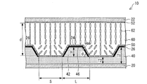
- FIG. 1 showing an embodiment of the present invention, is a cross-sectional view illustrating a schematic configuration of a liquid crystal display device.
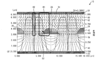
- FIG. 1 showing an embodiment of the present invention, is a cross-sectional view of a liquid crystal display device showing the alignment state and transmittance of liquid crystal molecules.
- FIG. 1 illustrates an embodiment of the present invention, and is a partial cross-sectional view of a liquid crystal display device illustrating an alignment state of liquid crystal molecules in the vicinity of an electrode interface.
- FIG. 1 illustrates an embodiment of the present invention, and is a partial cross-sectional view of a liquid crystal display device illustrating an alignment state of liquid crystal molecules in the vicinity of an electrode interface.
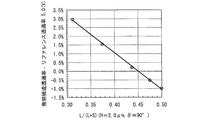
- FIG. 4 is a diagram illustrating an embodiment of the present invention, and is a diagram illustrating a relationship between setting of an electrode width L and an electrode interval S and an increase width of transmittance.
- FIG. 5 is a cross-sectional view of a liquid crystal display device, showing a second embodiment of the present invention and showing an alignment state and transmittance of liquid crystal molecules.
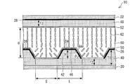
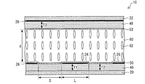
- FIG. 1 is a cross-sectional view of a liquid crystal display device 10 showing an embodiment of the present invention.
- the liquid crystal display device 10 is characterized in that a convex protrusion (convex structure) 42 having a trapezoidal cross-sectional shape is formed of an interlayer insulating film 40.
- the liquid crystal layer 60 including the positive liquid crystal molecules 62 is sandwiched between a pair of insulating substrates (array substrate 20 and counter substrate 22).
- the positive type liquid crystal molecule means a liquid crystal molecule having a positive dielectric anisotropy ⁇ .
- Alignment films 50 and 52 are provided on the surfaces of the array substrate 20 and the counter substrate 22 facing the liquid crystal layer 60, respectively.
- the vertical alignment film means an alignment film that makes liquid crystal molecules stand perpendicular to the film surface, and various materials such as an organic material and an inorganic material can be used as the material thereof.
- Examples of the vertical alignment film made of the above organic material include polymers in which side chains having vertical alignment properties (property to align (stand) liquid crystal molecules in the vertical direction with respect to the substrate) are bonded. That is, a material in which a group having vertical alignment properties is bonded to the polymer main chain as a side chain can be used as the vertical alignment film.
- a side chain having the vertical alignment for example, a side chain having a photoreactive functional group can be used.
- the photoreactive functional group include cinnamate groups represented by the following (Chemical Formula 1).
- the photoreactive functional group may constitute a side chain by itself or may constitute a part of the side chain. Moreover, when comprising a part of side chain, the said photoreactive functional group may be arrange
- the alignment process can be performed by light irradiation.
- the array substrate 20 is provided with electrodes (pixel electrode 24 and counter electrode 26) in a comb shape with an interlayer insulating film 40 interposed therebetween.
- the interlayer insulating film 40 is formed of a dielectric material such as acrylic resin.
- the pixel electrodes 24 and the counter electrodes 26 are alternately provided.
- the pixel electrode 24 and the counter electrode 26 have the same electrode width L in plan view, and adjacent electrodes are arranged at an interval indicated by an electrode interval S.
- the array substrate 20 is provided with active elements such as TFTs (Thin Film Transistors).
- TFTs Thin Film Transistors
- a convex protrusion 42 as a protrusion is provided between the array substrate 20 and the electrode.
- the material for forming the convex protrusions 42 is not particularly limited, but is formed of the interlayer insulating film 40 in the liquid crystal display device 10 of the present embodiment.
- the thickness of the interlayer insulating film 40 is different between a portion where the electrode is provided and a portion where the electrode is not provided.
- the thickness of the interlayer insulating film 40 between adjacent electrodes is T2 (interelectrode thickness of the interlayer insulating film), whereas the lower layer of the electrodes (the electrode and the array substrate 20)
- the thickness of the interlayer insulating film 40 of the intermediate layer is T1 (electrode portion thickness of the interlayer insulating film).
- H which is the difference between the electrode thickness T1 and the interelectrode thickness T2 is the height of the convex protrusion 42 (convex protrusion height H).
- the convex protrusion 42 has a trapezoidal cross-sectional shape. That is, the side surface (convex projection side surface) 44 of the convex protrusion 42 is inclined from the perpendicular direction of the array substrate 20.
- the convex protrusion 42 exemplifies a case where the cross-sectional shape is an isosceles trapezoid.
- the angle between the convex protrusion side surface 44 and the array substrate 20 is the base angle ⁇ .
- the electrodes (pixel electrode 24 and counter electrode 26) of the present embodiment are formed not only on the upper surface (convex projection upper surface 46) of the convex projection 42 but also on the convex projection side surface 44.
- electrodes are provided on the upper base and both sides of the trapezoid.
- the electrodes do not necessarily have to be provided on the entire surface (upper bottom and both sides (surface in contact with the liquid crystal layer)) of the convex protrusion 42.
- the transmittance can be improved by providing at least a part of the convex protrusion side surface 44. Further, the improvement in transmittance facilitates low voltage driving. This will be described below.
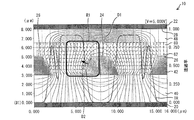
- FIG. 2 is a cross-sectional view of the liquid crystal display device 10 showing the alignment state of the liquid crystal molecules 62 in the liquid crystal display device 10 of the present embodiment.
- FIG. 2 is a view similar to FIG. 22 described above, and shows the alignment of the liquid crystal molecules 62 in a state where a voltage is applied to the electrodes. Further, TR in FIG. 2 indicates a transmittance line.
- the liquid crystal display device 10 is provided with the convex protrusions 42 and electrodes are also provided on the convex protrusion side surfaces 44 that are the side surfaces of the convex protrusions 42. This is a feature.
- the shape of the convex protrusion 42 is a trapezoid. Therefore, the convex protrusion side surface 44 is inclined from the vertical direction of the array substrate 20, that is, from the thickness direction of the liquid crystal layer 60. An electrode is provided on the convex protrusion side surface 44.
- the direction of the electric field indicated by the arrow D2 in FIG. 2 is likely to be a horizontal direction (an oblique direction) instead of a vertical direction.
- the liquid crystal molecules 62 are positive, the direction D2 of the electric field and the direction of the liquid crystal molecules 62 are substantially parallel. Therefore, in the liquid crystal display device 10 of the present embodiment, the liquid crystal molecules 62 in the vicinity of the electrode interface are likely to fall down.
- FIG. 3 shows the present embodiment and is a partial cross-sectional view of the liquid crystal display device 10 showing the alignment state of the liquid crystal molecules 62 in the vicinity of the electrode interface.
- the electric field direction D2 is in the lateral direction in the vicinity of the electrode interface, particularly in the vicinity of the convex protrusion side surface 44. Accordingly, the direction of the liquid crystal molecules 62 aligned in the same direction as the direction D2 of the electric field is also inclined in a direction parallel to the array substrate 20.
- the transmittance is improved in the above-mentioned electrode region R1 where dark lines are generated and the transmittance is likely to decrease.
- the transmittance of this portion is likely to be improved.
- the pixel electrode 24 is exemplified as the electrode, but the same applies to the case where the electrode is the counter electrode 26.
- the transmittance in the on-electrode region R1 is improved.
- the lateral electric field in the vicinity of the electrode interface that is, the orientation force in the lateral direction of the liquid crystal molecules 62 is improved, so that the transmittance in the center region R2 between the electrodes is easily improved.
- the transmittance is improved in the above-mentioned electrode upper region R1 and the inter-electrode center region R2 by comparing the transmittance line TR between FIG. 2 and FIG.
- the transmittance line TR in the vicinity of the inter-electrode center region R2 is compared in FIGS. 2 and 22, the transmittance line TR in FIG. 2 is more of the inter-electrode center region R2. It can be seen that the high position is maintained near and the transmittance near the inter-electrode center region R2 is improved.
- the convex protrusions 42 as the convex structure are provided, and the convex structure is covered with the electrodes. Therefore, the direction of the electric field near the side surface of the convex structure can be set to the horizontal direction or the oblique direction.
- the cell gap d, electrode width L, and electrode interval S shown in FIG. 1 and the like can be the same as those in a general TBA mode.
- the cell gap d is the same as the thickness of the liquid crystal layer 60 where the convex protrusions 42 do not exist.
- the cell gap d can be about 3.5 ⁇ m
- the electrode interval (space) S can be 4 to 10 ⁇ m
- the electrode width (line) L can be 2.5 to 4 ⁇ m.
- the transmittance is improved as the base angle ⁇ becomes smaller than 90 degrees regardless of the value of the height H of the convex protrusion.
- the transmittance tends to be improved as the convex protrusion height H is larger.
- the base angle ⁇ is preferably in a range from ⁇ min to 90 degrees as shown in FIG.
- FIGS. 6A to 6C are diagrams for explaining the range of the base angle ⁇ , and FIG. 6A shows the relationship between the electrode width L and the convex protrusion height H.
- FIG. 6B shows a convex projection model corresponding to the above formula, and
- FIG. 6C shows a preferable range of the base angle ⁇ .
- FIG. 7 is a diagram illustrating a relationship between the setting of the electrode width L and the electrode interval S and the increase width of the transmittance.
- the invention structure transmittance means the transmittance in the liquid crystal display device of the present embodiment provided with convex protrusions, while the reference transmittance means a liquid crystal of a flat electrode not provided with convex protrusions. It means the transmittance in the display device.
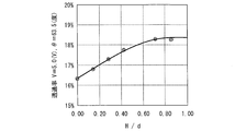
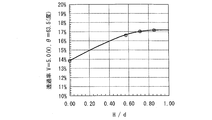
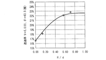
- FIGS. 8 and 9 are diagrams showing the relationship between the convex protrusion height H / cell gap d and the transmittance.
- the convex protrusion height H and the cell gap d are preferably H / d> 0 where a convex structure is provided as much as possible, more preferably 0 ⁇ H / d ⁇ 0.6.
- H / d satisfies 1> H / d.
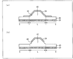
- FIGS. 10A and 10B are partial cross-sectional views of the liquid crystal display device according to the present embodiment.
- FIG. 10A shows a case where the electrode protrudes from the convex protrusion 42, and FIG. The case where the convex protrusion 42 could not be covered is shown.
- the pixel electrode 24 protrudes to the region of the electrode interval S in addition to covering the convex protrusion side surface 44.
- the transmittance improvement effect can be obtained as compared with the conventional structure (electrode flat structure).
- the substantial electrode width L is increased by the amount that the pixel electrode 24 protrudes into the region of the electrode interval S. Therefore, the effect of improving the transmittance is reduced. This is based on the basic characteristic of the TBA mode, that is, the transmittance decreases as the electrode width L increases.
- the end of the pixel electrode 24 is located on the convex protrusion side surface 44.
- the transmittance improvement effect can be obtained as compared with the conventional structure (electrode flat structure).
- the generation of the oblique electric field is reduced by the amount that the pixel electrode 24 cannot cover the convex protrusion 42.
- the effect of improving the transmittance is reduced as compared with the structure in which the entire surface of the convex protrusion 42 is covered with the pixel electrode 24, that is, without protruding.
- the effect of improving the transmittance is the highest when the convex protrusion 42 is covered with the electrodes (pixel electrode 24 and counter electrode 26). Whether it is covered too much or not covered, it is possible to achieve a transmittance higher than that of the conventional structure. This is because a lateral electric field (an oblique electric field) higher than that of the conventional structure can be generated as long as an electrode exists on at least a part of the convex protrusion side surface 44.
- the pixel electrode 24 is illustrated as an electrode. However, the same applies to the case where the electrode is the counter electrode 26.
- the shape of the convex protrusion 42 is not limited to a trapezoid.
- the cross-sectional shape of the convex protrusion 42 on the surface perpendicular to the array substrate 20 can be, for example, a trapezoid, a rectangle, a semi-ellipse, or the like.
- the shape of the convex protrusion 42 is a trapezoid or a rectangle, it may not be a trapezoid or a rectangle in a strict sense.
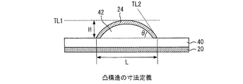
- FIG. 11 is a cross-sectional view of the convex protrusion 42 for explaining the dimensions of the convex protrusion 42.
- the convex protrusion height H can be defined as a distance between a portion where the convex protrusion 42 is not provided and the first tangent line TL1.
- the first tangent line TL1 is a tangent line at the maximum height portion of the convex protrusion 42 (a tangent line in a direction parallel to the surface of the array substrate 20).
- the base angle ⁇ can be defined as an angle formed by a plane direction (a direction parallel to the surface of the array substrate 20) where the convex protrusion 42 is not provided and the second tangent line TL2.
- the second tangent line TL2 is a tangent line of the convex protrusion 42 at a point where the convex protrusion 42 rises from a portion where the convex protrusion 42 is not provided (an end portion of the convex protrusion 42).
- the height H and the base angle ⁇ of the convex protrusion are illustrated so as to be defined with reference to the pixel electrode 24 provided on the surface of the convex protrusion 42.
- the film thickness of the pixel electrode 24 and the counter electrode 26 is extremely thinner than the height of the convex protrusion 42. Therefore, even with the measurement method shown in FIG. 11, the height H and the base angle ⁇ of the convex protrusion 42 can be substantially measured.
- the electrode width L shown in each figure such as FIG. 11 is based on the premise that the width of the bottom side of the convex protrusion 42 is equal to the electrode width when the electrode is provided over the entire surface of the convex protrusion 42. Yes. Therefore, when the electrode does not cover the entire surface of the convex protrusion 42, or when it protrudes from the convex protrusion 42, the width of the bottom side of the convex protrusion 42 does not match the electrode width. In this case, L in the figure and the like indicates the width of the bottom side of the convex protrusion 42.
- the liquid crystal display device 10 of the present embodiment is different from the liquid crystal display device 10 of the first embodiment in the structure of the counter substrate 22. That is, in the liquid crystal display device 10 of the first embodiment, only the vertical alignment film 52 is provided on the counter substrate 22. On the other hand, in the liquid crystal display device 10 of the present embodiment, the counter substrate 22 is provided with the interlayer insulating film 48 and the second counter electrode 28 in addition to the vertical alignment film 52. Specifically, the interlayer insulating film 48 and the second counter electrode 28 are provided over the entire surface of the counter substrate 22, specifically, the entire display region of the liquid crystal display device 10.
- FIG. 12 shows the liquid crystal display device 10 of the present embodiment, and is a cross-sectional view showing a schematic configuration of the liquid crystal display device 10.
- the second counter electrode 28 the interlayer insulating film 48, and the vertical alignment film 52 are provided on the counter substrate 22 in order in the direction facing the liquid crystal layer 60. It has been.
- the interlayer insulating film 40 provided on the array substrate 20 and the interlayer insulating film 48 are formed of the same material. Unlike the interlayer insulating film 40, the interlayer insulating film 48 is formed flat and has a film thickness T3 (thickness on the opposite side of the interlayer insulating film).
- the counter substrate 22 is also provided with a second counter electrode 28 that functions as a counter electrode in the same manner as the counter electrode 26. Therefore, the method of generating an electric field is different from the liquid crystal display device of the first embodiment shown in FIG.
- FIG. 13 is a cross-sectional view of the liquid crystal display device 10 showing the alignment state of the liquid crystal molecules 62 in the liquid crystal display device 10 of the present embodiment.
- FIG. 15 is a cross-sectional view of the liquid crystal display device 10 showing the alignment state of the liquid crystal molecules 62 in the liquid crystal display device 10 of the comparative form.
- FIG. 14 shows the configuration of the liquid crystal display device 10 according to the comparative example.
- the liquid crystal display device 10 of the comparative form shown in FIG. 14 and the liquid crystal display device 10 of the present embodiment are common in that the second counter electrode 28 is also provided on the counter substrate 22, but the array substrate 20. It is different whether or not the protrusions 42 are provided. In other words, the liquid crystal display device 10 of the comparative form is not provided with the convex protrusions 42, and the interlayer insulating film 48 of the array substrate 20 has a flat surface.
- the transmittance in the vicinity of the convex protrusions 42 is improved by the effect of the oblique electric field, as in the liquid crystal display device 10 of the first embodiment.
- the transmittance is improved in the electrode upper region R1 shown in FIG. 13 as compared with the electrode upper region R1 shown in FIG.
- the above improvement in transmittance is due to the difference in the alignment direction of the liquid crystal molecules 62. That is, in the liquid crystal display device 10 of the comparative form, as shown in FIG. 15, the liquid crystal molecules 62 are not easily tilted in the horizontal direction because the electric field direction D2 is vertical in the on-electrode region R1.
- the electric field direction D2 in the on-electrode region R1 shown in FIG. 13 tends to be in the horizontal (oblique) direction. Therefore, in this region, the liquid crystal molecules 62 easily fall down in the lateral direction. Therefore, the transmittance is improved in the on-electrode region R1.
- the electric field direction D2 in the vicinity of the electrode interface is close to the vertical direction as shown in FIG. Therefore, the liquid crystal molecules 62 are difficult to tilt.
- the transmittance in the above-mentioned electrode region R1 is improved.
- the conventional technique is used.
- the transmittance is improved as compared with a liquid crystal display device having a flat electrode structure. In other words, with respect to the base angle ⁇ , the transmittance is improved if the base angle ⁇ is a little.
- shape of convex protrusion In the above description, the case where the cross-sectional shape of the convex protrusion 42 is trapezoid has been described. However, the shape of the convex protrusion 42 is not limited to a trapezoid, and can be various shapes.
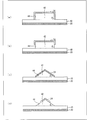
- FIGS. 20A to 20D illustrate convex protrusions 42 other than trapezoids.
- 20A and 20B are cross-sectional views of the liquid crystal display device.
- FIGS. 20A and 20B show a case where the convex protrusion is a rectangle
- FIGS. 20C and 13D show a case where the convex protrusion is a triangle. Show.
- the cross-sectional shape of the convex protrusion 42 can be not only a trapezoid but also various shapes such as a rectangle and a triangle.
- the base angle ⁇ is 90 degrees.
- the convex protrusions 42 are triangular, the convex protrusions 42 are substantially the same as when the convex protrusions 42 described above are trapezoidal. Since an oblique electric field is generated from the protruding side surface 44, the transmittance is improved as in the case of the trapezoid.
- the range of the base angle ⁇ when the convex protrusion 42 is a triangle is substantially the same as that when the convex protrusion 42 described above is a trapezoid. However, the base angle ⁇ ⁇ 90 degrees.
- the electrodes are provided so as to cover at least a part of the convex protrusion side surface 44.
- the covering method is not particularly limited.
- 20B and 20D illustrate a configuration in which the pixel electrode 24 covers only a part of the convex protrusion side surface 44 when the convex protrusion 42 is a rectangle and a triangle, respectively.
- the convex protrusion 42 is not necessarily provided by an interlayer insulating film, and can be formed by a material other than a material for forming the interlayer insulating film.
- examples of the material other than the interlayer insulating film include SiO X and SiN X (X is an integer).
- the liquid crystal display device of the present invention is It is preferable that the side surface of the protrusion has a portion inclined from a direction perpendicular to the substrate.
- the side surfaces are inclined, the effect of improving the transmittance can be obtained even when the electrode width is relatively wide.
- the liquid crystal display device of the present invention is When the height of the protrusion is H, the width of the base of the protrusion is L, and the base angle of the protrusion is ⁇ ,
- the base angle ⁇ can be tan ⁇ 1 (2H / L) ⁇ ⁇ ⁇ 90 degrees.
- the liquid crystal display device of the present invention is When the height of the protrusion is H and the thickness of the liquid crystal layer at a position where the protrusion is not provided is d,
- the ratio H / d between the height H and d is 0 ⁇ H / d ⁇ 1.
- the liquid crystal display device of the present invention is The ratio H / d is preferably 0.6 ⁇ H / d ⁇ 1.
- the protrusion having a height of at least the minimum height is provided. Therefore, a lateral (oblique) electric field is likely to be generated, and the transmittance is improved.
- the improvement range of the transmittance can be further increased.
- the liquid crystal display device of the present invention is The cross-sectional shape of the protrusion can be any of trapezoid, rectangle, and semi-ellipse.
- the said cross-sectional shape means the cross-sectional shape of the said protrusion in a surface perpendicular
- the liquid crystal display device of the present invention is An electrode can be provided so as to cover the entire surface of the protrusion.
- the entire surface including the side surface of the protrusion is covered with the electrode. Therefore, a lateral (oblique) electric field is more likely to be generated in the vicinity of the electrode interface, and a greater transmittance improvement effect can be obtained.
- the liquid crystal display device of the present invention is An active element can be provided on a substrate of the pair of substrates on which the protrusions are provided.
- the protrusion can be provided by the interlayer insulating film provided on the array substrate which is a substrate on which the active element is formed. Therefore, it becomes easy to form the protrusions.
- the liquid crystal display device of the present invention is The counter electrode can be provided on a second substrate, which is a substrate different from the substrate on which the protrusion is provided, of the pair of substrates.
- the liquid crystal display device of the present invention is A flat layer formed of a dielectric is provided on the second substrate,
- the counter electrode may be provided across the entire display region between the second substrate and the layer.
- the counter electrode is provided on the substrate facing the substrate on which the protrusions are provided.
- the electric field generated in the region on the electrode is laterally (obliquely) caused by the interaction between the counter electrode on the second substrate side and the pixel electrode on the first substrate side even when the side surface of the protrusion is at an angle close to vertical. It becomes possible to bend it.
- the transmittance is easily improved even when the side surface of the protrusion is at an angle close to perpendicular to the substrate.
- the present invention relates to a liquid crystal display device with improved transmittance, it can be suitably used for display applications that require high quality.
- Liquid crystal display device 20 Array substrate (Substrate) 22 Counter substrate (substrate) 24 pixel electrode (electrode) 26 Counter electrode (electrode) 28 Second counter electrode 40 Interlayer insulating film 42 Convex protrusion (protrusion) 44 Convex protrusion side face (protrusion side face) 46 convex protrusion upper surface 48 interlayer insulating film 50 alignment film 52 alignment film 60 liquid crystal layer 62 liquid crystal molecule 110 display device 112 substrate 114 interlayer insulating film 116 pixel electrode 118 counter electrode 120 recess S electrode interval L electrode width d cell gap D1 equipotential Line D2 Direction of electric field R1 Electrode region R2 Interelectrode central region H Convex protrusion height T1 Interlayer insulation film electrode thickness T2 Interlayer insulation film electrode thickness T3 Interlayer insulation film opposite side thickness TR transmission Rate line ⁇ Base angle TL1 First tangent TL2 Second tangent
Landscapes
- Physics & Mathematics (AREA)
- Nonlinear Science (AREA)
- Mathematical Physics (AREA)
- Chemical & Material Sciences (AREA)
- Crystallography & Structural Chemistry (AREA)
- General Physics & Mathematics (AREA)
- Optics & Photonics (AREA)
- Spectroscopy & Molecular Physics (AREA)
- Geometry (AREA)
- Liquid Crystal (AREA)
Abstract
本発明は、電極上領域(R1)における透過率が向上した液晶表示装置を提供することを目的とする。 本発明の液晶表示装置(10)は、アレイ基板(20)、対向基板(22)、及び液晶層(60)を備え、液晶分子(62)は、垂直配向膜(50)(52)によって基板に垂直な方向に初期配向しており、横電界で液晶分子(62)を制御して表示を行う。 アレイ基板(20)には、凸状突起(42)が設けられており、凸状突起(42)の側面(44)の少なくとも一部を覆うように、画素電極(24)及び対向電極(26)が設けられている。
Description
本発明は、表示品位の低下が抑制された液晶表示装置に関する。
櫛歯状の電極を備え、横電界を用いて表示する液晶表示装置が従来技術として知られている。
(特許文献1)
例えば、下記特許文献1には、同じ基板上に設けられた画素電極と対向電極との間に生じさせた電界で、液晶を駆動して表示を行う表示装置について記載されている。
例えば、下記特許文献1には、同じ基板上に設けられた画素電極と対向電極との間に生じさせた電界で、液晶を駆動して表示を行う表示装置について記載されている。
上記した、同じ基板上に画素電極と対向電極とが設けられている液晶表示装置において、電圧無印加の状態で垂直配向している液晶分子を用いて表示を行う表示モードが知られている。以下、上記表示モードをTBA(Transverse Bend Alignment)モードと称する。
このTBAモードでは、ポジ型の液晶分子を基板に対して垂直に配向させ、一方の基板に設けられた櫛歯状の電極(画素電極と対向電極)の間に横電界を発生させる。そして、液晶分子を基板と平行な方向(水平方向)に倒すことで、液晶表示装置を透過する光の量を制御する。
以下、図に基づいて、TBAモードの液晶表示装置の構成例について説明する。図21は、液晶表示装置の概略構成を示す断面図である。
図21に示すように、上記液晶表示装置10は、2枚の絶縁基板(アレイ基板20・対向基板22)とに液晶層60が挟持された構造を有している。
上記アレイ基板20には、画素電極24と対向電極26とが、層間絶縁膜40を介して、上記アレイ基板20上に、櫛歯状に交互に設けられている(櫛歯状電極)。詳しくは、上記画素電極24と対向電極26とは同じ幅(電極幅:L)を有している。そして、一定の間隔(電極間隔:S)で、上記層間絶縁膜40上に設けられている。
また、上記アレイ基板20及び対向基板22には、上記液晶層60に面するように配向膜50・52が設けられている。
TBAモードの液晶表示装置10では、上記配向膜50・52として、垂直配向膜が用いられている。また、上記液晶層60に含まれる液晶分子62は、ポジ型液晶分子である。
以上より、上記櫛歯状電極間に電圧が印加されていない初期配向状態では、上記液晶分子62は、基板に対して垂直方向に配向している。そして、上記櫛歯状電極間に電圧が印加されると、基板に対して平行若しくは斜め方向の横電界が発生する。液晶分子62がポジ型液晶分子であるので、液晶分子62は、上記電圧の印加により、基板に対して平行方向に傾斜する。
TBAモードでは、この様な液晶分子62の動きにより表示が行われる。
(暗線)
TBAモードによる表示では、明表示において暗線(光が透過しない部分)が発生するという問題がある。以下、液晶分子の配向状態を示す、液晶表示装置の断面図である図22に基づいて説明する。また、図22のTRは、透過率線を示している。
TBAモードによる表示では、明表示において暗線(光が透過しない部分)が発生するという問題がある。以下、液晶分子の配向状態を示す、液晶表示装置の断面図である図22に基づいて説明する。また、図22のTRは、透過率線を示している。
暗線は図22に示す電極上領域R1と、電極間中心領域R2とに生じうる。これは、上記透過率線TRが上記各領域で下降していることからもわかる。
ここで、上記電極上領域R1とは、液晶表示装置10の厚さ方向において、上記画素電極24又は上記対向電極26の上層の領域を意味する。
また、上記電極間中心領域R2とは、上記画素電極24と上記対向電極26との間(電極間)の中央近傍の上層の領域を意味する。
(電極上領域R1)
まず、上記電極上領域R1に発生する暗線について説明する。
まず、上記電極上領域R1に発生する暗線について説明する。
電極に電圧を印加した際、電極界面から生じる電界の向きは、電極界面に対して垂直となる。そのため、上記図22に示すように電極(画素電極24・対向電極26)が平坦である場合には、電極界面の近傍の電界の向きは矢印D2(電界の向き)で示すように、アレイ基板20に対して垂直な方向となる。なお、図22に示す線D1は、等電位線を示している。
そして、液晶分子62がポジ型液晶分子であるため、電界の向きD2と、液晶分子62の向きとは、平行となる。
図23は、電極界面近傍での液晶分子の配向状態を示す、液晶表示装置の部分断面図である。
上記図23に示すように、画素電極24の近傍では電界の向きD2がアレイ基板20と垂直に近い方向、すなわち縦方向となり、横電界が生じにくい。そのため、電界の向きD2と同方向となる液晶分子62の向きも、縦方向となる。
以上のように、電極界面の近傍では、有効な横電界が生じないため、液晶分子62が倒れない。その結果、透過率が向上せず、暗線として観察されやすい。
なお、上記図23では、電極として画素電極24を例示したが、電極が対向電極26である場合も同様である。
(電極間中心領域R2)
つぎに、上記電極間中心領域R2に発生する暗線について説明する。この電極間中心領域R2には、上記電極上領域R1とは異なり、横電界が生じやすい。
つぎに、上記電極間中心領域R2に発生する暗線について説明する。この電極間中心領域R2には、上記電極上領域R1とは異なり、横電界が生じやすい。
しかし、上記電極上領域R1を挟んでその両側から液晶分子62が倒れようとするため、液晶分子62がぶつかり合い、液晶分子62が縦方向に配向したままになりやすい。
そのため、上記電極の間の中心部は、透過率が向上せず、暗線として観察されやすい。
以上のように、TBAモードでは、電極の中央部分近傍(電極上領域R1)で電界の向きが水平にならず、液晶分子が倒れないために、暗線が生じやすい。
また、隣接する電極の間の部分近傍(電極間中心領域R2)では、液晶分子が左向きに倒れようとする力と右向きに倒れようとする力とが等しくなりやすいので、液晶分子が倒れないため、暗線が生じやすい。
そこで本発明は、上記課題を解決するためになされたものであり、その目的は、暗線の発生を抑制して、透過率が向上した液晶表示装置を提供することにある。特には、上記電極上領域R1における透過率が向上した液晶表示装置を提供することにある。
本発明の液晶表示装置は、上記課題を解決するために、
一対の基板と、上記一対の基板に挟持された液晶層とを備え、
上記液晶層に含まれる液晶分子は、上記基板に対して垂直な方向に初期配向しており、
上記液晶分子の配向を、横電界で制御して表示を行う液晶表示装置であって、
上記一対の基板の少なくとも一方の基板には、誘電体で形成された突起が設けられており、
上記突起の側面の少なくとも一部を覆うように、電極が設けられていることを特徴としている。
一対の基板と、上記一対の基板に挟持された液晶層とを備え、
上記液晶層に含まれる液晶分子は、上記基板に対して垂直な方向に初期配向しており、
上記液晶分子の配向を、横電界で制御して表示を行う液晶表示装置であって、
上記一対の基板の少なくとも一方の基板には、誘電体で形成された突起が設けられており、
上記突起の側面の少なくとも一部を覆うように、電極が設けられていることを特徴としている。
上記の構成によれば、突起の側面に電極が設けられているので、電極界面近傍に横(斜め)電界が生じやすい。そのため、液晶分子が横(斜め)方向に傾斜しやすくなるので、その部分における透過率が向上する。
したがって、透過率、特には、電極近傍における透過率が向上した液晶表示装置を実現することができる。
本発明の液晶表示装置は、以上のように、一対の基板の少なくとも一方の基板には、誘電体で形成された突起が設けられており、上記突起の側面の少なくとも一部を覆うように、電極が設けられているものである。
それゆえ、暗線の発生を抑制して、透過率が向上した液晶表示装置を実現することができるという効果を奏する。
以下、本発明の実施の形態について、詳細に説明する。
〔実施の形態1〕
以下、本発明の第1の実施の形態について図1から図11に基づいて説明する。
以下、本発明の第1の実施の形態について図1から図11に基づいて説明する。
図1は、本発明の実施の形態を示す液晶表示装置10の断面図である。
本実施の形態の液晶表示装置10は、その断面形状が台形である凸状突起(凸構造)42が、層間絶縁膜40で形成されていることを特徴とする。
(概略構成)
本実施の形態の液晶表示装置10は、上記図1に示すように、ポジ型の液晶分子62を含む液晶層60が、一対の絶縁性を有する基板(アレイ基板20・対向基板22)に挟持された構造を有している。上記ポジ型の液晶分子とは、誘電異方性Δεが正の液晶分子を意味する。
本実施の形態の液晶表示装置10は、上記図1に示すように、ポジ型の液晶分子62を含む液晶層60が、一対の絶縁性を有する基板(アレイ基板20・対向基板22)に挟持された構造を有している。上記ポジ型の液晶分子とは、誘電異方性Δεが正の液晶分子を意味する。
そして、上記アレイ基板20及び対向基板22の上記液晶層60に面する面には、配向膜50・52が各々設けられている。
本実施の形態の液晶表示装置10は、先に説明した、TBAモードの液晶表示装置10であるため、上記配向膜50・52には、垂直配向膜が用いられている。垂直配向膜とは、膜面に対して液晶分子を垂直に立たせるような配向膜を意味し、その材料としては、有機材料、無機材料等種々の材料を用いることができる。
上記の有機材料からなる垂直配向膜として、垂直配向性(基板に対して液晶分子を垂直方向に配向させる(立たせる)性質)を有する側鎖が結合されているポリマーを例示することができる。すなわち、垂直配向性を有する基が、側鎖としてポリマー主鎖に結合されている材料を垂直配向膜として用いることができる。
また、上記垂直配向性を有する側鎖として、例えば光反応性官能基を有する側鎖を用いることができる。上記光反応性官能基としては、例えば下記(化1)に示すシンナメート基が挙げられる。
また、上記光反応性官能基は、それのみで側鎖を構成していてもよいし、或いは側鎖の一部分を構成していてもよい。また、側鎖の一部分を構成している場合には、上記光反応性官能基は、側鎖のどの部分に配置されていても良い。
なお、光反応性官能基を有するポリマーを配向膜として用いる場合、その配向処理を光照射で行うことができる。

また、上記アレイ基板20には、層間絶縁膜40を介して、電極(画素電極24と対向電極26)が櫛歯状に設けられている。
なお、上記層間絶縁膜40は、アクリル系樹脂等の誘電体で形成されている。
具体的には、画素電極24と対向電極26とが交互に設けられている。図1では、上記画素電極24及び対向電極26は、平面視において同じ電極幅Lであり、電極間隔Sで示す間隔で、隣接する電極は配置されている。
また、上記アレイ基板20には、TFT(Thin Film Transistor)等のアクティブ素子が設けられている。
(凸状突起)
本実施の形態の液晶表示装置10では、上記アレイ基板20と電極との間に、突起としての凸状突起42が設けられている。この凸状突起42を形成する材料は、特には限定されないが、本実施の形態の液晶表示装置10では、上記層間絶縁膜40で形成されている。
本実施の形態の液晶表示装置10では、上記アレイ基板20と電極との間に、突起としての凸状突起42が設けられている。この凸状突起42を形成する材料は、特には限定されないが、本実施の形態の液晶表示装置10では、上記層間絶縁膜40で形成されている。
すなわち、上記電極が設けられている部分と、上記電極が設けられていない部分とで、上記層間絶縁膜40の厚さが異なる。
具体的には、隣接する電極の間の層間絶縁膜40の厚さは、T2(層間絶縁膜の電極間部厚さ)であるのに対して、上記電極の下層(電極とアレイ基板20との間の層)の層間絶縁膜40の厚さは、T1(層間絶縁膜の電極部厚さ)となっている。
そして、上記電極部厚さT1と、上記電極間部厚さT2との差であるHが、上記凸状突起42の高さ(凸状突起高さH)である。
また、上記凸状突起42は、その断面形状が台形となっている。すなわち、上記凸状突起42の側面(凸状突起側面)44は、アレイ基板20の垂線方向から傾斜している。
本実施の形態においては、図1に示すように、上記凸状突起42は、その断面形状が等脚台形である場合を例示している。そして、上記凸状突起側面44とアレイ基板20との角度が底角θである。
(電極)
また、本実施の形態の電極(画素電極24・対向電極26)は、上記凸状突起42の上面(凸状突起上面46)のみならず、上記凸状突起側面44にも形成されている。
また、本実施の形態の電極(画素電極24・対向電極26)は、上記凸状突起42の上面(凸状突起上面46)のみならず、上記凸状突起側面44にも形成されている。
すなわち、台形における上底及び両側辺にあたる部分に、電極が設けられている。
なお、上記電極は、必ずしも上記凸状突起42の全表面(上底及び両側辺(液晶層と接する表面))に設けられている必要はない。ただ、上記凸状突起側面44の少なくとも一部に設けられていることにより、透過率を向上させることができる。また、透過率の向上は、低電圧駆動を容易にする。以下説明する。
(液晶分子の配向)
図2は、本実施の形態の液晶表示装置10における液晶分子62の配向状態を示す、液晶表示装置10の断面図である。
図2は、本実施の形態の液晶表示装置10における液晶分子62の配向状態を示す、液晶表示装置10の断面図である。
図2は、先に説明した図22と同様の図であり、電極に電圧が印加された状態での液晶分子62の配向などを示している。また、図2のTRは、透過率線を示している。
本実施の形態の液晶表示装置10は、先に説明したように、凸状突起42が設けられているとともに、その凸状突起42の側面である凸状突起側面44にも、電極が設けられている点が特徴である。
電極に電圧を印加した際、電極界面から生じる電界の向きは、電極界面に対して垂直となる。上記液晶表示装置10では、凸状突起42の形状が台形である。そのため、凸状突起側面44は、アレイ基板20の垂直方向、すなわち液晶層60の厚さ方向から傾斜している。そして、その凸状突起側面44に電極が設けられている。
そのため、図2に矢印D2として示す電界の向きが、縦方向ではなく、横方向(斜め方向)となりやすい。
ここで、TBAモードの液晶表示装置10では、液晶分子62がポジ型であるので、上記電界の向きD2と、液晶分子62の向きとがほぼ平行になる。そのため、本実施の形態の液晶表示装置10では、電極界面近傍での液晶分子62が倒れやすい。
図3に基づいて説明する。図3は、本実施の形態を示すものであり、電極界面近傍での液晶分子62の配向状態を示す、液晶表示装置10の部分断面図である。
図3に示すように、電極界面近傍、特には上記凸状突起側面44の近傍において、電界の向きD2が横方向になっている。それに伴い、上記電界の向きD2と同じ方向に配向する液晶分子62の向きも、アレイ基板20と平行な方向に傾斜した向きとなっている。
これにより、本実施の形態の液晶表示装置10では、暗線が生じ、透過率が低下しやすい上記電極上領域R1において、透過率が向上する。特には、電極の両端近傍に横電界が発生しやすくなるので、この部分の透過率が向上しやすい。なお、上記図3では、電極として画素電極24を例示したが、電極が対向電極26である場合も同様である。
以上のように、本実施の形態の液晶表示装置10では、電極上領域R1での透過率が向上する。
また、上記電極界面近傍での横電界、引いては液晶分子62の横方向への配向力が向上することにより、上記電極間中心領域R2での透過率も向上しやすい。
このように、上記電極上領域R1及び電極間中心領域R2で透過率が向上することは、上記図2と上記図22とで、その透過率線TRを比較することでもわかる。
すなわち、図2と図22とで、上記電極上領域R1における透過率線TRを比較すると、図2における透過率線TRの方が、山型の肩が立っており、透過率が向上していることがわかる。
また、同様に、図2と図22とで、上記電極間中心領域R2の近傍部分における透過率線TRを比較すると、図2における透過率線TRの方が、より上記電極間中心領域R2の近くまで高い位置を維持しており、上記電極間中心領域R2近傍の透過率が向上していることがわかる。
以上のように、本実施の形態の液晶表示装置10では、凸構造としての凸状突起42が設けられ、またその凸構造が電極で覆われている。そのため、凸構造の側面付近の電界の向きを横方向、又は斜め方向にすることができる。
したがって、電極の端の部分である、凸構造の側面部分に横電界が生じやすくなる。よって、ON表示において、その部分に暗線が生じにくく、透過率が向上しやすくなる。
その結果、液晶表示装置10全体として透過率が向上する。
(寸法例)
つぎに、本実施の形態の液晶表示装置10の寸法例について説明する。
つぎに、本実施の形態の液晶表示装置10の寸法例について説明する。
上記図1等に示したセルギャップd、電極幅L、電極間隔Sは、一般的なTBAモードと同様のもとをすることができる。なお、上記セルギャップdは、凸状突起42が存在しない部分の液晶層60の厚さと同じである。
具体的には、例えば、セルギャップd:3.5μm程度、電極間隔(スペース)S:4~10μm、電極幅(ライン)L:2.5~4μmとすることができる。
つぎに、上記凸状突起42の形状を特徴付けるパラメータ、凸状突起高さH、及び底角θについて説明する。
以下の説明は、次の材料・構成を前提としている。液晶材料の屈折率異方性Δn=0.1、液晶材料の誘電率異方性Δε=22、層間絶縁膜の電極部厚さT1=3.0μm、層間絶縁膜の誘電率=3.3、セルギャップd=3.5μm。
(L:S=4.0:4.0μm)
図4に基づいて、電極幅L=4.0μm、電極間隔S=4.0μm、印加電圧=5.0Vの際の、透過率の底角(電極底角)θに対する依存性を示す。上記図4は、L:S=4.0:4.0μmにおける底角θと透過率との関係を示す図である。
図4に基づいて、電極幅L=4.0μm、電極間隔S=4.0μm、印加電圧=5.0Vの際の、透過率の底角(電極底角)θに対する依存性を示す。上記図4は、L:S=4.0:4.0μmにおける底角θと透過率との関係を示す図である。
上記図4に示すように、凸状突起高さHの値にかかわらず、底角θが90度よりも小さくなるにつれて、透過率が向上する。
また、底角θの値が同じ場合、凸状突起高さHが大きい方が、透過率が向上しやすい傾向がある。
(L:S=2.5:5.5μm)
つぎに、図5に基づいて、電極幅L=2.5μm、電極間隔S=5.5μm、印加電圧=5.0Vの際の、透過率の底角(電極底角)θに対する依存性を示す。上記図5は、上記図4と同様の図であり、L:S=2.5:5.5μmにおける底角θと透過率との関係を示す図である。
つぎに、図5に基づいて、電極幅L=2.5μm、電極間隔S=5.5μm、印加電圧=5.0Vの際の、透過率の底角(電極底角)θに対する依存性を示す。上記図5は、上記図4と同様の図であり、L:S=2.5:5.5μmにおける底角θと透過率との関係を示す図である。
上記図5に示すように、L:S=2.5:5.5μmの場合であっても、L:S=4.0:4.0μmの場合と同様に、底角θが90度よりも小さくなるにつれて、透過率が向上する傾向にある。そして、この傾向は、凸状突起高さHが大きい方が強い。
また、底角θの値が同じ場合、凸状突起高さHが大きい方が、透過率が向上しやすい傾向も、上記L:S=4.0:4.0μmの場合と同様である。
(底角θの範囲)
上記図4及び図5に示すように、凸状突起高さHにかかわらず、底角θが90度よりも小さくなるほど透過率向上の効果が大きくなるとの傾向がある。ただ、凸状突起高さHに対して底角θは、図6の(b)に示すように、凸状突起の凸構造の形状が三角形になるところまでしか取り得ない。そこで、底角θの最小値をθminとすると、θminは、図6の(a)に示す式で表すことができる。
上記図4及び図5に示すように、凸状突起高さHにかかわらず、底角θが90度よりも小さくなるほど透過率向上の効果が大きくなるとの傾向がある。ただ、凸状突起高さHに対して底角θは、図6の(b)に示すように、凸状突起の凸構造の形状が三角形になるところまでしか取り得ない。そこで、底角θの最小値をθminとすると、θminは、図6の(a)に示す式で表すことができる。
以上より、底角θは、図6の(c)に示すように、θminから90度までの範囲が好ましい範囲となる。
なお、図6の(a)から(c)は、底角θの範囲について説明するための図であり、図6の(a)は電極幅Lと凸状突起高さHとの関係を表す数式を示し、図6の(b)は上記数式に対応する凸状突起のモデルを示し、(c)は底角θの好ましい範囲を示している。
(θ=90度の場合)
なお、上記図4に示した、L:S=4.0:4.0μmの場合では、底角θ=90度のとき、凸状突起高さHが大きくなるほど、透過率が小さくなっている。
なお、上記図4に示した、L:S=4.0:4.0μmの場合では、底角θ=90度のとき、凸状突起高さHが大きくなるほど、透過率が小さくなっている。
これは、底角θ=90度のまま、凸状突起高さHが大きくなることは、斜め電界が生じない状態で単純に電極部分のセルギャップdを縮めることになる。そのため、リタデーションがl/2条件から著しく離れ、電極部分の透過率を下げることになるためと考えられる。
したがって、電極部分の全体に占める割合が小さくなるようなL:Sを設定すれば、底角θ=90度において凸状突起高さHが大きくなっても、凸状突起すなわち凸構造なしの平坦電極の場合(リファレンス)以上の透過率を得ることができる。
上述の、電極部分の全体に占める割合が小さくなるようなL:Sについて、図7に基づいて説明する。図7は、電極幅L・電極間隔Sの設定と、透過率の上昇幅との関係を示す図である。詳しくは、凸状突起高さH=2.0μm、底角θ=90度の場合において、L/(L+S)と、印加電圧=5Vでの透過率の上昇幅(発明構造透過率-リファレンス透過率)との関係を示している。なお発明構造透過率とは、凸状突起が設けられた本実施の形態の液晶表示装置における透過率を意味し、他方、リファレンス透過率とは、凸状突起が設けられていない平坦電極の液晶表示装置における透過率を意味している。
上記図7に示すように、L/(L+S)を小さくして、電極部分の全体に占める割合を小さくしていくと、具体的には、例えば、L/(L+S)が0.45程度以下となると、底角θ=90度の場合において凸状突起高さHが大きくなっても、平坦電極の液晶表示装置以上の透過率を得ることができる。
(L:Sの設定)
なお、電極幅Lと電極間隔Sとの値は、特に限定されるものではないが、上記各例では、電極幅Lと電極間隔Sとの和が8μmである場合を例示した。また、電極幅Lの上限は4.0μm、下限は2.5μmとした。
なお、電極幅Lと電極間隔Sとの値は、特に限定されるものではないが、上記各例では、電極幅Lと電極間隔Sとの和が8μmである場合を例示した。また、電極幅Lの上限は4.0μm、下限は2.5μmとした。
これは、電極幅Lが4.0μmを超えると、開口率減少による透過率ロスが大きくなるためと、電極幅Lが2.5μmを下回ると、量産性に問題が生じうるからである。
(凸状突起高さH)
つぎに、図8及び図9に基づいて、凸状突起高さH/セルギャップdと透過率との関係について説明する。図8及び図9は、いずれも凸状突起高さH/セルギャップdと透過率との関係を示す図である。図8はL:S=4.0:4.0μmの場合を示し、図9はL:S=2.5:5.5μmの場合を示している。なお、底角θ=63.4度、及び、印加電圧=5.0Vである点は、図8及び図9に共通である。
つぎに、図8及び図9に基づいて、凸状突起高さH/セルギャップdと透過率との関係について説明する。図8及び図9は、いずれも凸状突起高さH/セルギャップdと透過率との関係を示す図である。図8はL:S=4.0:4.0μmの場合を示し、図9はL:S=2.5:5.5μmの場合を示している。なお、底角θ=63.4度、及び、印加電圧=5.0Vである点は、図8及び図9に共通である。
上記図8及び図9に示すように、凸状突起高さが少しでもあれば、言い換えると、H/d>0であれば、従来の平坦な電極構造を有する液晶表示装置よりも透過率が向上するという効果があることがわかる。特には、0<H/d<0.6で透過率の向上効果が大きい。H/d≧0.6では透過率の向上効果は飽和する傾向にある。
以上より、凸状突起高さH・セルギャップdは、少しでも凸構造が設けられているH/d>0が好ましく、より好ましくは、0<H/d<0.6となる。なお、凸状突起高さHは、上記セルギャップdを超えることはないため、H/dは、1>H/dとなる。
(凸状突起と電極)
つぎに、図10の(a)及び(b)に基づいて、電極(画素電極24・対向電極26)の凸状突起42の覆い方について説明する。図10の(a)及び(b)は、本実施の形態の液晶表示装置の部分断面図であり、(a)は電極が凸状突起42からはみ出した場合を示し、(b)は電極が凸状突起42を覆いきれなかった場合を示している。
つぎに、図10の(a)及び(b)に基づいて、電極(画素電極24・対向電極26)の凸状突起42の覆い方について説明する。図10の(a)及び(b)は、本実施の形態の液晶表示装置の部分断面図であり、(a)は電極が凸状突起42からはみ出した場合を示し、(b)は電極が凸状突起42を覆いきれなかった場合を示している。
図10の(a)に示す、画素電極24が凸状突起42からはみ出した構造では、画素電極24が凸状突起側面44を覆うのに加えて、電極間隔Sの領域にまではみ出している。
上記のような構造であっても、従来構造(電極平坦構造)に比べて、透過率の改善効果は得られる。ただし、このような構造の場合、画素電極24が電極間隔Sの領域にはみ出した分だけ、実質的な電極幅Lが大きくなる。そのため、透過率の改善効果が小さくなる。これは、TBAモードの基本的な特性である、電極幅Lが大きくなると、それに伴い透過率が低下するとの特性に基づくものである。
他方、図10の(b)に示す、画素電極24が凸状突起42を覆いきれなかった構造では、画素電極24の端部が、凸状突起側面44上に位置している。
上記のような構造であっても、従来構造(電極平坦構造)に比べて、透過率の改善効果は得られる。ただし、このような構造の場合、画素電極24が凸状突起42を覆えなかった分だけ斜め電界の発生が少なくなる。そのため、透過率の改善効果は、凸状突起42の全表面がちょうど、すなわちはみ出すことなく、画素電極24で覆われている構造に比べて小さくなる。
以上のように、透過率の改善効果が最も高いのは、凸状突起42がちょうど電極(画素電極24・対向電極26)で覆われている場合であるが、凸状突起42を、電極が覆いすぎた場合でも、覆いきれなかった場合でも、従来の構造以上の透過率を達成することができる。これは、凸状突起側面44の少なくとも一部分に電極が存在する限り、従来の構造以上の横電界(斜め電界)を発生させることができるためである。
なお、上記図10の(a)及び(b)では、電極として画素電極24を例示したが、電極が対向電極26である場合であっても同様である。
(凸状突起の寸法)
以上の説明では、凸状突起42の高さH、及び、底角θについて、台形の凸状突起42に基づいて説明した。
以上の説明では、凸状突起42の高さH、及び、底角θについて、台形の凸状突起42に基づいて説明した。
ただ、凸状突起42の形状は台形に限定されるものではない。凸状突起42の上記アレイ基板20と垂直な面における断面形状は、例えば、台形,長方形,半楕円形等とすることができる。
また、凸状突起42の形状が、台形又は長方形であっても、厳密な意味での台形又は長方形ではないこともありうる。
そこで、上記凸状突起高さHと底角θとを一般化すると、図11のように表すことができる。図11は、凸状突起42の寸法について説明するための、凸状突起42の断面図である。
まず、凸状突起高さHは、上記図11に示すように、凸状突起42が設けられていない部分と、第1接線TL1との距離として定義することができる。ここで、上記第1接線TL1は、凸状突起42の最大高さ部分における接線(アレイ基板20の表面と平行な方向の接線)である。
一方、底角θは、凸状突起42が設けられていない部分の平面方向(アレイ基板20の表面と平行な方向)と、第2接線TL2とのなす角として定義することができる。ここで、上記第2接線TL2は、凸状突起42が、凸状突起42の設けられていない部分から立ち上がる点(凸状突起42の端部)における、凸状突起42の接線である。
なお、上記図11では、上記凸状突起高さH及び底角θについて、凸状突起42の表面に設けられた画素電極24を基準にして定義されるように図示されている。
ただ、一般的に画素電極24や対向電極26の膜厚は、凸状突起42の高さよりも、極めて薄い。そのため、図11に示した測定方法であっても、実質的に、凸状突起42の高さH及び底角θを測定することができる。
なお、上記図11など各図で示す電極幅Lは、凸状突起42の全表面にわたって電極が設けられた場合に、凸状突起42の底辺の幅と電極幅とが等しくなることを前提としている。そのため、電極が凸状突起42の全表面を覆わない場合や、凸状突起42からはみ出す場合には、凸状突起42の底辺の幅と電極幅とは一致しない。その場合、図等におけるLは、凸状突起42の底辺の幅を示している。
〔実施の形態2〕
本発明の液晶表示装置10に関する他の実施の形態について、図12~図19に基づいて説明すれば、以下のとおりである。
本発明の液晶表示装置10に関する他の実施の形態について、図12~図19に基づいて説明すれば、以下のとおりである。
なお、説明の便宜上、上記実施の形態1で説明した図面と同じ機能を有する部材については、同じ符号を付記し、その説明を省略する。
本実施の形態の液晶表示装置10は、上記実施の形態1の液晶表示装置10と比較して、対向基板22の構造が相違する。すなわち、上記実施の形態1の液晶表示装置10では、対向基板22には、垂直配向膜52が設けられているのみであった。これに対して本実施の形態の液晶表示装置10では、対向基板22に、垂直配向膜52に加えて、層間絶縁膜48及び第2対向電極28が設けられている。具体的には、対向基板22の全面、詳しくは液晶表示装置10の表示領域の全体にわたって、層間絶縁膜48及び第2対向電極28が設けられている。
図12に基づいて具体的に説明する。図12は、本実施の形態の液晶表示装置10を示すものであり、液晶表示装置10の概略構成を示す断面図である。図12に示すように、本実施の形態の液晶表示装置10では、対向基板22に、液晶層60に面する方向に順に、第2対向電極28、層間絶縁膜48、垂直配向膜52が設けられている。
アレイ基板20に設けられている層間絶縁膜40と、上記層間絶縁膜48とは、同じ材料で形成されている。また、上記層間絶縁膜48は、上記層間絶縁膜40とは異なり、平坦に形成されおり、その膜厚はT3(層間絶縁膜の対向側厚さ)である。
(液晶分子の配向)
つぎに、本実施の形態の液晶表示装置10における液晶分子62の配向状態について説明する。
つぎに、本実施の形態の液晶表示装置10における液晶分子62の配向状態について説明する。
上記液晶表示装置10では、対向基板22にも上記対向電極26と同様に対向電極として機能する第2対向電極28が設けられている。そのため、上記図2に示した第1の実施の形態の液晶表示装置と、電界の発生の仕方が相違する。
図13は、本実施の形態の液晶表示装置10における液晶分子62の配向状態を示す、液晶表示装置10の断面図である。
また、図15は、比較の形態の液晶表示装置10における液晶分子62の配向状態を示す、液晶表示装置10の断面図である。そして上記比較の形態の液晶表示装置10の構成を、図14に示す。
図14に示す比較の形態の液晶表示装置10と、本実施の形態の液晶表示装置10とは、対向基板22にも第2対向電極28が設けられている点は共通するが、アレイ基板20に凸状突起42が設けられているか否かが相違する。すなわち、比較の形態の液晶表示装置10には、凸状突起42は設けられておらず、アレイ基板20の層間絶縁膜48は平坦な表面を有している。
本実施の形態の液晶表示装置10でも、第1の実施形態の液晶表示装置10と同様に、斜め電界の効果により凸状突起42近傍の透過率が向上する。
すなわち、特には、図13に示す電極上領域R1において、図15に示す電極上領域R1よりも透過率が向上する。
これは、上記図13と図15とで、電極上領域R1における透過率線TRを比較することでわかる。すなわち、画素電極24に対する相対位置が同じ電極上領域R1において、図15に示す透過率線TRは、画素電極24に遠い位置から下降し始めるのに対して、図13に示す透過率線TRは、より画素電極24に近い位置まで高い位置を保っている。
以上のような透過率の向上は、液晶分子62の配向方向の相違による。すなわち、比較の形態の液晶表示装置10では、図15に示すように、電極上領域R1で、電界の向きD2が縦方向なので液晶分子62が横方向に倒れにくい。
これに対して、本実施の形態の液晶表示装置10では、図13に示す電極上領域R1での電界の向きD2が横(斜め)方向になりやすい。そのため、この領域で、液晶分子62が横方向に倒れやすくなる。よって、上記電極上領域R1で、透過率が向上する。
(電極界面近傍)
なお、電極界面近傍での液晶分子の配向状態は、上記図3及び図23に示したものとほぼ同様である。
なお、電極界面近傍での液晶分子の配向状態は、上記図3及び図23に示したものとほぼ同様である。
すなわち、上記図12に示した液晶表示装置10では、図3に示すように、電極界面近傍に横(斜め)方向の電界が発生しやすく、上記電界の向きD2と同じ向きに配向する液晶分子62も斜め方向に配向しやすい。
一方、上記図14に示した液晶表示装置10では、図23に示すように、電極界面近傍の電界の向きD2は、垂直方向に近い。そのため、液晶分子62は傾斜し難い。
以上より、本実施の形態の液晶表示装置10では、上記電極上領域R1での透過率が向上する。
(透過率変化)
つぎに、図16~図19に基づいて、寸法例と透過率との関係について説明する。
つぎに、図16~図19に基づいて、寸法例と透過率との関係について説明する。
図16及び図17は、それぞれ実施の形態1における図4及び図5に対応し、図16は、L:S=4.0:4.0μmにおける底角θと透過率との関係を示す図であり、図17は、L:S=2.5:5.5μmにおける底角θと透過率との関係を示す図である。
また、同様に、図18及び図19は、それぞれ実施の形態1における図8及び図9に対応し、図18は、L:S=4.0:4.0μmにおける凸状突起高さH/セルギャップdと透過率との関係を示し、図19は、L:S=2.5:5.5μmにおける凸状突起高さH/セルギャップdと透過率との関係を示す図である。
用いた材料や液晶表示装置の構成等は、特に言及しない場合には、上記実施の形態1と同様である。
上記各図に示すように、凸状突起高さHが大きくなると、上記実施の形態1と同様に、透過率がより高くなる傾向にある。
また、凸状突起高さH/セルギャップdと透過率との関係についても、上記実施の形態1と同様に、凸状突起高さHが少しでもあれば(H/d>0)、従来の平坦な電極構造を有する液晶表示装置よりも透過率が向上する。言い換えると、底角θに関して、少しでも底角θをもてば、透過率は向上する。
なお、その透過率の向上効果は、特に、0<H/d<0.6でその効果が大きい。そして、H/d≧0.6では透過率の向上効果は飽和する傾向にある。
(凸状突起の形状)
なお、上記の説明では、凸状突起42の断面形状が台形である場合について説明した。ただ、凸状突起42の形状は台形に限定されるものではなく、種々の形状とすることが可能である。
なお、上記の説明では、凸状突起42の断面形状が台形である場合について説明した。ただ、凸状突起42の形状は台形に限定されるものではなく、種々の形状とすることが可能である。
図20の(a)から(d)に、台形以外の凸状突起42を例示する。図20は液晶表示装置の断面図であり、(a)及び(b)は、凸状突起が長方形である場合を示し、(c)及び(d)は、凸状突起が三角形である場合を示している。
図20に示すように、凸状突起42の断面形状は、台形のみならず、長方形や三角形等種々の形状とすることができる。
上記図20の(a)及び(b)に示すように、凸状突起42が長方形である場合には、底角θが90度となる。
凸状突起42が長方形である場合には、凸状突起側面44から、隣接する凸状突起42の凸状突起側面44に向かって、横方向の電界が生じやすい。そのため、液晶分子62が倒れやすくなるので、透過率が向上しやすい。
また、上記図20の(c)及び(d)に示すように、凸状突起42が三角形である場合には、先に説明した凸状突起42が台形である場合とほぼ同様に、凸状突起側面44から斜め方向の電界が生じるので、台形である場合と同様に透過率が向上する。
なお、凸状突起42が三角形である場合の底角θの範囲は、先に説明した凸状突起42が台形である場合とほぼ同様になる。ただし、底角θ<90度となる。
(電極の覆い方)
また、凸状突起42の形状が台形でない場合であっても、先に説明したとおり、電極(画素電極24や対向電極26)は、凸状突起側面44の少なくとも一部分を覆うよう設けられていれば良く、特にその覆い方は限定されるものではない。
また、凸状突起42の形状が台形でない場合であっても、先に説明したとおり、電極(画素電極24や対向電極26)は、凸状突起側面44の少なくとも一部分を覆うよう設けられていれば良く、特にその覆い方は限定されるものではない。
図20の(b)及び(d)は、各々、凸状突起42が長方形及び三角形の場合に、画素電極24が凸状突起側面44の一部分のみを覆っている構成を例示している。
また、上記凸状突起42は、必ずしも層間絶縁膜で設けられる必要はなく、層間絶縁膜を形成する材料以外の材料で形成することもできる。例えば、層間絶縁膜以外の材料としては、SiOX,SiNX (Xは整数)等を例示することができる。
本発明は上記した各実施の形態に限定されるものではなく、請求項に示した範囲で種々の変更が可能であり、異なる実施の形態にそれぞれ開示された技術的手段を適宜組み合わせて得られる実施の形態についても本発明の技術的範囲に含まれる。
本発明の液晶表示装置は、
上記突起の側面が、基板に対して垂直な方向から傾斜している部分を有していることが好ましい。
上記突起の側面が、基板に対して垂直な方向から傾斜している部分を有していることが好ましい。
上記の構成によれば、側面が傾斜しているので、側面が垂直の場合よりも電極上領域において横電界が発生しやすく、その結果、透過率をより向上させることができる。
また、側面が傾斜しているので、電極幅を比較的広くした場合であっても、透過率向上の効果を得ることができる。
また、本発明の液晶表示装置は、
上記突起の高さをH、突起の底辺の幅をL、突起の底角をθとした場合、
上記底角θを、tan-1(2H/L)≦θ≦90度とすることができる。
上記突起の高さをH、突起の底辺の幅をL、突起の底角をθとした場合、
上記底角θを、tan-1(2H/L)≦θ≦90度とすることができる。
また、本発明の液晶表示装置は、
上記突起の高さをHとし、上記突起が設けられていない位置での液晶層の厚さをdとした場合、
上記高さHとdとの比H/dが、0<H/d<1であることを特徴とする。
上記突起の高さをHとし、上記突起が設けられていない位置での液晶層の厚さをdとした場合、
上記高さHとdとの比H/dが、0<H/d<1であることを特徴とする。
また、本発明の液晶表示装置は、
上記比H/dが、0.6≦H/d<1であることが好ましい。
上記比H/dが、0.6≦H/d<1であることが好ましい。
上記の構成によれば、少なくとも最小高さ以上の高さを有する突起が設けられている。そのため、横(斜め)電界が生じやすくなるので、透過率が向上する。
また、比H/dが、0.6≦H/d<1である場合には、透過率の向上幅をより大きくすることができる。
また、本発明の液晶表示装置は、
上記突起の断面形状を台形,長方形,半楕円形のうちのいずれかとすることができる。
上記突起の断面形状を台形,長方形,半楕円形のうちのいずれかとすることができる。
なお、上記断面形状は、上記突起が設けられている基板と垂直な面における、上記突起の断面形状を意味する。
また、本発明の液晶表示装置は、
上記突起の全表面を覆うように、電極を設けることができる。
上記突起の全表面を覆うように、電極を設けることができる。
上記の構成によれば、突起の側面を含めて、全表面が電極で覆われている。そのため、電極界面近傍に横(斜め)電界がより生じやすくなり、より大きな透過率向上効果を得ることができる。
本発明の液晶表示装置は、
上記一対の基板のうちの、上記突起が設けられている基板に、アクティブ素子を設けることができる。
上記一対の基板のうちの、上記突起が設けられている基板に、アクティブ素子を設けることができる。
上記の構成によれば、アクティブ素子が形成される基板であるアレイ基板に設けられる層間絶縁膜で、上記突起を設けることができる。そのため、突起の形成が容易になる。
また、本発明の液晶表示装置は、
上記一対の基板のうちの、上記突起が設けられている基板とは異なる基板である第2基板に、対向電極を設ることができる。
上記一対の基板のうちの、上記突起が設けられている基板とは異なる基板である第2基板に、対向電極を設ることができる。
また、本発明の液晶表示装置は、
上記第2基板に、誘電体で形成された平坦な層を設け、
上記対向電極を、上記第2基板と上記層との間に、表示領域全体にわたるように設けることができる。
上記第2基板に、誘電体で形成された平坦な層を設け、
上記対向電極を、上記第2基板と上記層との間に、表示領域全体にわたるように設けることができる。
上記の構成によれば、突起が設けられている基板と対向する基板に、対向電極が設けられている。
これにより、第2基板側の対向電極と第1基板側の画素電極との相互作用により、突起の側面が垂直に近い角度であっても、電極上領域に発生する電界を横(斜め)方向に曲げることが可能となる。
そのため、突起の側面が、基板に対して垂直に近い角度であっても、透過率が向上しやすくなる。
本発明は、透過率が向上した液晶表示装置に関するものであるので、高品位が要求されるディスプレイ用途に、好適に利用することができる。
10 液晶表示装置
20 アレイ基板 (基板)
22 対向基板 (基板)
24 画素電極 (電極)
26 対向電極 (電極)
28 第2対向電極
40 層間絶縁膜
42 凸状突起 (突起)
44 凸状突起側面(突起の側面)
46 凸状突起上面
48 層間絶縁膜
50 配向膜
52 配向膜
60 液晶層
62 液晶分子
110 表示装置
112 基板
114 層間絶縁膜
116 画素電極
118 対向電極
120 凹部
S 電極間隔
L 電極幅
d セルギャップ
D1 等電位線
D2 電界の向き
R1 電極上領域
R2 電極間中心領域
H 凸状突起高さ
T1 層間絶縁膜の電極部厚さ
T2 層間絶縁膜の電極間部厚さ
T3 層間絶縁膜の対向側厚さ
TR 透過率線
θ 底角
TL1 第1接線
TL2 第2接線
20 アレイ基板 (基板)
22 対向基板 (基板)
24 画素電極 (電極)
26 対向電極 (電極)
28 第2対向電極
40 層間絶縁膜
42 凸状突起 (突起)
44 凸状突起側面(突起の側面)
46 凸状突起上面
48 層間絶縁膜
50 配向膜
52 配向膜
60 液晶層
62 液晶分子
110 表示装置
112 基板
114 層間絶縁膜
116 画素電極
118 対向電極
120 凹部
S 電極間隔
L 電極幅
d セルギャップ
D1 等電位線
D2 電界の向き
R1 電極上領域
R2 電極間中心領域
H 凸状突起高さ
T1 層間絶縁膜の電極部厚さ
T2 層間絶縁膜の電極間部厚さ
T3 層間絶縁膜の対向側厚さ
TR 透過率線
θ 底角
TL1 第1接線
TL2 第2接線
Claims (10)
- 一対の基板と、上記一対の基板に挟持された液晶層とを備え、
上記液晶層に含まれる液晶分子は、上記基板に対して垂直な方向に初期配向しており、
上記液晶分子の配向を、横電界で制御して表示を行う液晶表示装置であって、
上記一対の基板の少なくとも一方の基板には、誘電体で形成された突起が設けられており、
上記突起の側面の少なくとも一部を覆うように、電極が設けられていることを特徴とする液晶表示装置。 - 上記突起の側面が、基板に対して垂直な方向から傾斜している部分を有していることを特徴とする請求項1に記載の液晶表示装置。
- 上記突起の高さをH、突起の底辺の幅をL、突起の底角をθとした場合、
上記底角θが、tan-1(2H/L)≦θ≦90度であることを特徴とする請求項1に記載の液晶表示装置。 - 上記突起の高さをHとし、上記突起が設けられていない位置での液晶層の厚さをdとした場合、
上記高さHとdとの比H/dが、0<H/d<1であることを特徴とする請求項1から3のいずれか1項に記載の液晶表示装置。 - 上記比H/dが、0.6≦H/d<1であることを特徴とする請求項4に記載の液晶表示装置。
- 上記突起の、当該突起が設けられている上記基板と垂直な面における断面形状が、台形,長方形,半楕円形のうちのいずれかであることを特徴とする請求項1から5のいずれか1項に記載の液晶表示装置。
- 上記突起の全表面を覆うように、電極が設けられていることを特徴とする請求項1から6のいずれか1項に記載の液晶表示装置。
- 上記一対の基板のうちの、上記突起が設けられている基板に、アクティブ素子が設けられていることを特徴とする請求項1から7のいずれか1項に記載の液晶表示装置。
- 上記一対の基板のうちの、上記突起が設けられている基板とは異なる基板である第2基板に、対向電極が設けられていることを特徴とする請求項1から8のいずれか1項に記載の液晶表示装置。
- 上記第2基板に、誘電体で形成された平坦な層が設けられており、
上記対向電極は、上記第2基板と上記層との間に、表示領域全体にわたって設けられていることを特徴とする請求項9に記載の液晶表示装置。
Priority Applications (1)
| Application Number | Priority Date | Filing Date | Title |
|---|---|---|---|
| US13/813,780 US20130293817A1 (en) | 2010-08-02 | 2011-07-26 | Liquid crystal display device |
Applications Claiming Priority (2)
| Application Number | Priority Date | Filing Date | Title |
|---|---|---|---|
| JP2010173581 | 2010-08-02 | ||
| JP2010-173581 | 2010-08-02 |
Publications (1)
| Publication Number | Publication Date |
|---|---|
| WO2012017863A1 true WO2012017863A1 (ja) | 2012-02-09 |
Family
ID=45559366
Family Applications (1)
| Application Number | Title | Priority Date | Filing Date |
|---|---|---|---|
| PCT/JP2011/066973 Ceased WO2012017863A1 (ja) | 2010-08-02 | 2011-07-26 | 液晶表示装置 |
Country Status (2)
| Country | Link |
|---|---|
| US (1) | US20130293817A1 (ja) |
| WO (1) | WO2012017863A1 (ja) |
Families Citing this family (1)
| Publication number | Priority date | Publication date | Assignee | Title |
|---|---|---|---|---|
| CN105093379A (zh) * | 2014-05-21 | 2015-11-25 | 远东新世纪股份有限公司 | 微位相差膜 |
Citations (5)
| Publication number | Priority date | Publication date | Assignee | Title |
|---|---|---|---|---|
| JPH09258265A (ja) * | 1996-03-19 | 1997-10-03 | Sharp Corp | 液晶表示装置 |
| JP2000305100A (ja) * | 1999-02-15 | 2000-11-02 | Fujitsu Ltd | 液晶表示装置 |
| JP2002139735A (ja) * | 2000-10-31 | 2002-05-17 | Fujitsu Ltd | 液晶表示パネル及びその開発方法 |
| JP2002139736A (ja) * | 2000-10-31 | 2002-05-17 | Sanyo Electric Co Ltd | 液晶表示装置 |
| JP2005106967A (ja) * | 2003-09-29 | 2005-04-21 | Hitachi Ltd | 液晶表示装置 |
Family Cites Families (2)
| Publication number | Priority date | Publication date | Assignee | Title |
|---|---|---|---|---|
| TWI251697B (en) * | 1999-05-26 | 2006-03-21 | Matsushita Electric Industrial Co Ltd | Liquid crystal display element and producing method thereof |
| US7113241B2 (en) * | 2001-08-31 | 2006-09-26 | Sharp Kabushiki Kaisha | Liquid crystal display and method of manufacturing the same |
-
2011
- 2011-07-26 US US13/813,780 patent/US20130293817A1/en not_active Abandoned
- 2011-07-26 WO PCT/JP2011/066973 patent/WO2012017863A1/ja not_active Ceased
Patent Citations (5)
| Publication number | Priority date | Publication date | Assignee | Title |
|---|---|---|---|---|
| JPH09258265A (ja) * | 1996-03-19 | 1997-10-03 | Sharp Corp | 液晶表示装置 |
| JP2000305100A (ja) * | 1999-02-15 | 2000-11-02 | Fujitsu Ltd | 液晶表示装置 |
| JP2002139735A (ja) * | 2000-10-31 | 2002-05-17 | Fujitsu Ltd | 液晶表示パネル及びその開発方法 |
| JP2002139736A (ja) * | 2000-10-31 | 2002-05-17 | Sanyo Electric Co Ltd | 液晶表示装置 |
| JP2005106967A (ja) * | 2003-09-29 | 2005-04-21 | Hitachi Ltd | 液晶表示装置 |
Also Published As
| Publication number | Publication date |
|---|---|
| US20130293817A1 (en) | 2013-11-07 |
Similar Documents
| Publication | Publication Date | Title |
|---|---|---|
| TWI483047B (zh) | 顯示裝置 | |
| TWI505004B (zh) | 畫素結構 | |
| CN103713432B (zh) | 显示装置及电子设备 | |
| CN101859044B (zh) | 具有提高的显示质量的显示装置 | |
| CN202256974U (zh) | 一种边缘场开关模式的液晶显示面板 | |
| CN101395525B (zh) | 液晶显示装置 | |
| CN101968590B (zh) | 液晶显示面板 | |
| CN101339311B (zh) | 液晶装置及电子机器 | |
| WO2019010996A1 (zh) | 阵列基板及显示装置 | |
| JP2007025661A (ja) | マルチドメイン垂直配向型液晶表示装置 | |
| CN103488003A (zh) | 一种阵列基板及其制作方法、液晶面板及显示装置 | |
| US20120176575A1 (en) | Liquid crystal display element | |
| JP5963564B2 (ja) | 液晶表示装置 | |
| US8284359B2 (en) | Liquid crystal panel and liquid crystal display device | |
| WO2012017863A1 (ja) | 液晶表示装置 | |
| JP5172691B2 (ja) | 液晶表示装置 | |
| JP2005024676A (ja) | 液晶表示装置 | |
| US20090207358A1 (en) | Horizontal-switching flexible liquid crystal displays and fabrication methods thereof | |
| JP4386105B2 (ja) | 液晶表示装置 | |
| CN203480176U (zh) | 一种阵列基板、液晶面板及显示装置 | |
| JP5488950B2 (ja) | 横電界方式のアクティブマトリクス型液晶表示装置 | |
| JP2004301879A (ja) | 液晶表示装置 | |
| US20150009459A1 (en) | Liquid crystal display panel and liquid crystal display device | |
| CN106802521B (zh) | 像素结构、阵列基板和液晶显示面板 | |
| WO2011129247A1 (ja) | 液晶表示装置 |
Legal Events
| Date | Code | Title | Description |
|---|---|---|---|
| 121 | Ep: the epo has been informed by wipo that ep was designated in this application |
Ref document number: 11814491 Country of ref document: EP Kind code of ref document: A1 |
|
| NENP | Non-entry into the national phase |
Ref country code: DE |
|
| WWE | Wipo information: entry into national phase |
Ref document number: 13813780 Country of ref document: US |
|
| 122 | Ep: pct application non-entry in european phase |
Ref document number: 11814491 Country of ref document: EP Kind code of ref document: A1 |
|
| NENP | Non-entry into the national phase |
Ref country code: JP |