WO2012017648A1 - Plasma display panel driving method and plasma display apparatus - Google Patents
Plasma display panel driving method and plasma display apparatus Download PDFInfo
- Publication number
- WO2012017648A1 WO2012017648A1 PCT/JP2011/004389 JP2011004389W WO2012017648A1 WO 2012017648 A1 WO2012017648 A1 WO 2012017648A1 JP 2011004389 W JP2011004389 W JP 2011004389W WO 2012017648 A1 WO2012017648 A1 WO 2012017648A1
- Authority
- WO
- WIPO (PCT)
- Prior art keywords
- voltage
- discharge
- electrode
- sustain
- gradation value
- Prior art date
Links
Images


Classifications
-
- G—PHYSICS
- G09—EDUCATION; CRYPTOGRAPHY; DISPLAY; ADVERTISING; SEALS
- G09G—ARRANGEMENTS OR CIRCUITS FOR CONTROL OF INDICATING DEVICES USING STATIC MEANS TO PRESENT VARIABLE INFORMATION
- G09G3/00—Control arrangements or circuits, of interest only in connection with visual indicators other than cathode-ray tubes
- G09G3/20—Control arrangements or circuits, of interest only in connection with visual indicators other than cathode-ray tubes for presentation of an assembly of a number of characters, e.g. a page, by composing the assembly by combination of individual elements arranged in a matrix no fixed position being assigned to or needed to be assigned to the individual characters or partial characters
- G09G3/22—Control arrangements or circuits, of interest only in connection with visual indicators other than cathode-ray tubes for presentation of an assembly of a number of characters, e.g. a page, by composing the assembly by combination of individual elements arranged in a matrix no fixed position being assigned to or needed to be assigned to the individual characters or partial characters using controlled light sources
- G09G3/28—Control arrangements or circuits, of interest only in connection with visual indicators other than cathode-ray tubes for presentation of an assembly of a number of characters, e.g. a page, by composing the assembly by combination of individual elements arranged in a matrix no fixed position being assigned to or needed to be assigned to the individual characters or partial characters using controlled light sources using luminous gas-discharge panels, e.g. plasma panels
- G09G3/288—Control arrangements or circuits, of interest only in connection with visual indicators other than cathode-ray tubes for presentation of an assembly of a number of characters, e.g. a page, by composing the assembly by combination of individual elements arranged in a matrix no fixed position being assigned to or needed to be assigned to the individual characters or partial characters using controlled light sources using luminous gas-discharge panels, e.g. plasma panels using AC panels
- G09G3/291—Control arrangements or circuits, of interest only in connection with visual indicators other than cathode-ray tubes for presentation of an assembly of a number of characters, e.g. a page, by composing the assembly by combination of individual elements arranged in a matrix no fixed position being assigned to or needed to be assigned to the individual characters or partial characters using controlled light sources using luminous gas-discharge panels, e.g. plasma panels using AC panels controlling the gas discharge to control a cell condition, e.g. by means of specific pulse shapes
- G09G3/293—Control arrangements or circuits, of interest only in connection with visual indicators other than cathode-ray tubes for presentation of an assembly of a number of characters, e.g. a page, by composing the assembly by combination of individual elements arranged in a matrix no fixed position being assigned to or needed to be assigned to the individual characters or partial characters using controlled light sources using luminous gas-discharge panels, e.g. plasma panels using AC panels controlling the gas discharge to control a cell condition, e.g. by means of specific pulse shapes for address discharge
-
- G—PHYSICS
- G09—EDUCATION; CRYPTOGRAPHY; DISPLAY; ADVERTISING; SEALS
- G09G—ARRANGEMENTS OR CIRCUITS FOR CONTROL OF INDICATING DEVICES USING STATIC MEANS TO PRESENT VARIABLE INFORMATION
- G09G3/00—Control arrangements or circuits, of interest only in connection with visual indicators other than cathode-ray tubes
- G09G3/20—Control arrangements or circuits, of interest only in connection with visual indicators other than cathode-ray tubes for presentation of an assembly of a number of characters, e.g. a page, by composing the assembly by combination of individual elements arranged in a matrix no fixed position being assigned to or needed to be assigned to the individual characters or partial characters
- G09G3/22—Control arrangements or circuits, of interest only in connection with visual indicators other than cathode-ray tubes for presentation of an assembly of a number of characters, e.g. a page, by composing the assembly by combination of individual elements arranged in a matrix no fixed position being assigned to or needed to be assigned to the individual characters or partial characters using controlled light sources
- G09G3/28—Control arrangements or circuits, of interest only in connection with visual indicators other than cathode-ray tubes for presentation of an assembly of a number of characters, e.g. a page, by composing the assembly by combination of individual elements arranged in a matrix no fixed position being assigned to or needed to be assigned to the individual characters or partial characters using controlled light sources using luminous gas-discharge panels, e.g. plasma panels
- G09G3/288—Control arrangements or circuits, of interest only in connection with visual indicators other than cathode-ray tubes for presentation of an assembly of a number of characters, e.g. a page, by composing the assembly by combination of individual elements arranged in a matrix no fixed position being assigned to or needed to be assigned to the individual characters or partial characters using controlled light sources using luminous gas-discharge panels, e.g. plasma panels using AC panels
- G09G3/291—Control arrangements or circuits, of interest only in connection with visual indicators other than cathode-ray tubes for presentation of an assembly of a number of characters, e.g. a page, by composing the assembly by combination of individual elements arranged in a matrix no fixed position being assigned to or needed to be assigned to the individual characters or partial characters using controlled light sources using luminous gas-discharge panels, e.g. plasma panels using AC panels controlling the gas discharge to control a cell condition, e.g. by means of specific pulse shapes
- G09G3/294—Control arrangements or circuits, of interest only in connection with visual indicators other than cathode-ray tubes for presentation of an assembly of a number of characters, e.g. a page, by composing the assembly by combination of individual elements arranged in a matrix no fixed position being assigned to or needed to be assigned to the individual characters or partial characters using controlled light sources using luminous gas-discharge panels, e.g. plasma panels using AC panels controlling the gas discharge to control a cell condition, e.g. by means of specific pulse shapes for lighting or sustain discharge
-
- G—PHYSICS
- G09—EDUCATION; CRYPTOGRAPHY; DISPLAY; ADVERTISING; SEALS
- G09G—ARRANGEMENTS OR CIRCUITS FOR CONTROL OF INDICATING DEVICES USING STATIC MEANS TO PRESENT VARIABLE INFORMATION
- G09G2320/00—Control of display operating conditions
- G09G2320/02—Improving the quality of display appearance
- G09G2320/0238—Improving the black level
-
- G—PHYSICS
- G09—EDUCATION; CRYPTOGRAPHY; DISPLAY; ADVERTISING; SEALS
- G09G—ARRANGEMENTS OR CIRCUITS FOR CONTROL OF INDICATING DEVICES USING STATIC MEANS TO PRESENT VARIABLE INFORMATION
- G09G2320/00—Control of display operating conditions
- G09G2320/02—Improving the quality of display appearance
- G09G2320/0271—Adjustment of the gradation levels within the range of the gradation scale, e.g. by redistribution or clipping
-
- G—PHYSICS
- G09—EDUCATION; CRYPTOGRAPHY; DISPLAY; ADVERTISING; SEALS
- G09G—ARRANGEMENTS OR CIRCUITS FOR CONTROL OF INDICATING DEVICES USING STATIC MEANS TO PRESENT VARIABLE INFORMATION
- G09G2320/00—Control of display operating conditions
- G09G2320/04—Maintaining the quality of display appearance
- G09G2320/041—Temperature compensation
-
- G—PHYSICS
- G09—EDUCATION; CRYPTOGRAPHY; DISPLAY; ADVERTISING; SEALS
- G09G—ARRANGEMENTS OR CIRCUITS FOR CONTROL OF INDICATING DEVICES USING STATIC MEANS TO PRESENT VARIABLE INFORMATION
- G09G2320/00—Control of display operating conditions
- G09G2320/04—Maintaining the quality of display appearance
- G09G2320/043—Preventing or counteracting the effects of ageing
-
- G—PHYSICS
- G09—EDUCATION; CRYPTOGRAPHY; DISPLAY; ADVERTISING; SEALS
- G09G—ARRANGEMENTS OR CIRCUITS FOR CONTROL OF INDICATING DEVICES USING STATIC MEANS TO PRESENT VARIABLE INFORMATION
- G09G3/00—Control arrangements or circuits, of interest only in connection with visual indicators other than cathode-ray tubes
- G09G3/20—Control arrangements or circuits, of interest only in connection with visual indicators other than cathode-ray tubes for presentation of an assembly of a number of characters, e.g. a page, by composing the assembly by combination of individual elements arranged in a matrix no fixed position being assigned to or needed to be assigned to the individual characters or partial characters
- G09G3/2007—Display of intermediate tones
- G09G3/2044—Display of intermediate tones using dithering
-
- G—PHYSICS
- G09—EDUCATION; CRYPTOGRAPHY; DISPLAY; ADVERTISING; SEALS
- G09G—ARRANGEMENTS OR CIRCUITS FOR CONTROL OF INDICATING DEVICES USING STATIC MEANS TO PRESENT VARIABLE INFORMATION
- G09G3/00—Control arrangements or circuits, of interest only in connection with visual indicators other than cathode-ray tubes
- G09G3/20—Control arrangements or circuits, of interest only in connection with visual indicators other than cathode-ray tubes for presentation of an assembly of a number of characters, e.g. a page, by composing the assembly by combination of individual elements arranged in a matrix no fixed position being assigned to or needed to be assigned to the individual characters or partial characters
- G09G3/22—Control arrangements or circuits, of interest only in connection with visual indicators other than cathode-ray tubes for presentation of an assembly of a number of characters, e.g. a page, by composing the assembly by combination of individual elements arranged in a matrix no fixed position being assigned to or needed to be assigned to the individual characters or partial characters using controlled light sources
- G09G3/28—Control arrangements or circuits, of interest only in connection with visual indicators other than cathode-ray tubes for presentation of an assembly of a number of characters, e.g. a page, by composing the assembly by combination of individual elements arranged in a matrix no fixed position being assigned to or needed to be assigned to the individual characters or partial characters using controlled light sources using luminous gas-discharge panels, e.g. plasma panels
- G09G3/288—Control arrangements or circuits, of interest only in connection with visual indicators other than cathode-ray tubes for presentation of an assembly of a number of characters, e.g. a page, by composing the assembly by combination of individual elements arranged in a matrix no fixed position being assigned to or needed to be assigned to the individual characters or partial characters using controlled light sources using luminous gas-discharge panels, e.g. plasma panels using AC panels
- G09G3/296—Driving circuits for producing the waveforms applied to the driving electrodes
- G09G3/2965—Driving circuits for producing the waveforms applied to the driving electrodes using inductors for energy recovery
Definitions
- the present invention relates to an AC surface discharge type plasma display panel driving method and a plasma display apparatus.
- a typical plasma display panel (hereinafter abbreviated as “panel”) as a display device has a large number of discharge cells formed between a front substrate and a rear substrate arranged to face each other.
- a plurality of pairs of display electrodes composed of a pair of scan electrodes and sustain electrodes are formed on the front glass substrate in parallel with each other.
- a dielectric layer and a protective layer are formed so as to cover the display electrode pairs.
- the back substrate has a plurality of parallel data electrodes formed on the glass substrate on the back side, a dielectric layer is formed so as to cover the data electrodes, and a plurality of barrier ribs are formed thereon in parallel with the data electrodes. ing. And the fluorescent substance layer is formed in the surface of a dielectric material layer, and the side surface of a partition.
- the front substrate and the rear substrate are arranged opposite to each other and sealed so that the display electrode pair and the data electrode are three-dimensionally crossed.
- a discharge gas containing xenon at a partial pressure ratio of 5% is sealed, and a discharge cell is formed in a portion where the display electrode pair and the data electrode face each other.
- ultraviolet rays are generated by gas discharge in each discharge cell, and the phosphors of each color of red (R), green (G) and blue (B) are excited and emitted by the ultraviolet rays. Display an image.
- the subfield method is generally used as a method for driving the panel.
- one field is divided into a plurality of subfields, and light emission and non-light emission of each discharge cell are controlled in each subfield.
- gradation display is performed by controlling the number of times of light emission generated in one field.
- Each subfield has an initialization period, an address period, and a sustain period.
- an initialization waveform is applied to each scan electrode, and an initialization operation is performed to generate an initialization discharge in each discharge cell.
- wall charges necessary for the subsequent address operation are formed, and priming particles (excited particles for generating the discharge) for generating the address discharge stably are generated.
- Initializing operation includes forced initializing operation that generates initializing discharge in each discharge cell regardless of the operation of the previous subfield, and initializing discharge is generated only in the discharge cell that has generated address discharge in the immediately preceding subfield. There is a selective initialization operation to do.
- an address discharge is selectively generated in the discharge cells according to the image to be displayed, and an address operation is performed to form wall charges in the discharge cells.
- scan pulses are sequentially applied to the scan electrodes, and address pulses are selectively applied to the data electrodes based on the image signal to be displayed. Thereby, an address discharge is generated between the scan electrode and the data electrode of the discharge cell to emit light, and a wall charge is formed in the discharge cell.
- the sustain pulses of the number based on the luminance weight determined for each subfield are alternately applied to the display electrode pairs composed of the scan electrodes and the sustain electrodes, and the sustain discharge is generated in the discharge cells that have generated the address discharge.
- the sustaining operation for causing the phosphor layer of the discharge cell to emit light is performed (hereinafter, the discharge cell is caused to emit light by the sustain discharge is also referred to as “lighting” and the light emission is not referred to as “non-lighting”).
- each discharge cell is made to emit light with the luminance according to the luminance weight.
- the light emission of the phosphor layer due to the sustain discharge is light emission related to gradation display, and the other light emission is light emission not related to gradation display.
- each discharge cell of the panel is caused to emit light with a luminance corresponding to the gradation value of the image signal, and an image is displayed in the image display area of the panel.
- One of the important factors in improving the image display quality on the panel is the improvement in contrast.
- light emission not related to gradation display is reduced as much as possible, the luminance when displaying the lowest gradation (black gradation value “0”) is reduced, and the contrast ratio is improved.
- a driving method is disclosed.
- the forced initialization operation is performed using a gradually changing ramp waveform voltage.
- the forced initializing operation is performed in the initializing period of one subfield, and the selective initializing operation is performed in the initializing period of the other subfield. In this way, the number of times of forced initialization operation is set to once per field.
- black luminance The luminance of the black display area where no sustain discharge occurs (hereinafter abbreviated as “black luminance”) varies depending on light emission not related to image display, for example, light emission caused by initialization discharge.
- light emission in the black display region is only weak light emission when the initialization operation is performed on all the discharge cells. Thereby, it is possible to reduce the black luminance and display an image with high contrast (see, for example, Patent Document 1).
- the number of forced initialization operations per unit time (for example, 1 second) can be reduced and the black luminance can be further decreased as compared with the driving method described in Patent Document 1. it can.
- the wall charge necessary for generating the address discharge in the subsequent address period is accumulated in the discharge cell, and the discharge delay time is shortened to surely generate the address discharge.
- the discharge delay time is the time required from when the voltage applied to the discharge cell exceeds the discharge start voltage until the actual discharge occurs. The longer the discharge delay time, the more unstable the generation of discharge.
- the address discharge operation becomes unstable due to a long discharge delay time of the address discharge, or a malfunction such as no address discharge occurs, resulting in normal image display. become unable.
- the present invention is a panel driving method for driving a panel having a plurality of discharge cells each having a scan electrode, a sustain electrode, and a data electrode.
- a single field is formed by using a plurality of subfields each having an address period, a sustain period, and an erase period.
- a scan pulse is applied to the scan electrode and an address pulse is applied to the data electrode. This is applied to selectively generate an address discharge in the discharge cell, and in the sustain period, sustain pulses of the number corresponding to the luminance weight are alternately applied to the scan electrode and the sustain electrode to maintain the address discharge in the discharge cell.
- a ramp waveform voltage is applied to the scan electrode, and an erasing discharge is selectively generated only in the discharge cells in which the address discharge is generated in the immediately preceding address period.
- the voltage obtained by subtracting the voltage applied to the data electrode from the low-voltage side voltage of the sustain pulse applied to the scan electrode during the sustain period is defined as the first voltage, and the data is obtained from the high-voltage side voltage of the sustain pulse applied to the scan electrode during the sustain period
- the voltage obtained by subtracting the voltage applied to the electrode is the second voltage
- the voltage obtained by subtracting the low voltage side voltage of the write pulse applied to the data electrode from the low voltage side voltage of the scan pulse applied to the scan electrode in the write period is the third voltage.
- the voltage applied to each electrode is set so that the voltage obtained by subtracting the third voltage from the first voltage is equal to or higher than the discharge start voltage of the discharge using the data electrode as an anode and the scan electrode as a cathode.
- a voltage obtained by subtracting the third voltage from the second voltage is a discharge start voltage of discharge using the data electrode as an anode and the scan electrode as a cathode, and the data electrode as a cathode and the scan electrode as an anode.
- the discharge start voltage of the discharge to the sum following sets the voltage applied to the electrodes.
- the input image signal is amplified at a predetermined amplification factor and an image is displayed on the panel. At this time, an input image signal less than a predetermined size is amplified with an amplification factor equal to or higher than an amplification factor for an input image signal having a predetermined size or more.
- the panel driving method of the present invention it is desirable to increase the amplification factor as the input image signal becomes smaller for an input image signal less than a predetermined size.
- the predetermined size may be a size in which only the subfield having the smallest luminance weight in one field emits light and the other subfields do not emit light.
- the temperature of the panel is detected and the detected temperature is compared with a preset temperature threshold value.
- the detected temperature is You may enlarge the amplification factor regarding the input image signal below a predetermined magnitude
- the cumulative operation time of the panel is measured and the measured cumulative operation time is compared with a preset cumulative time threshold value.
- the amplification factor relating to an input image signal having a size less than a predetermined magnitude may be larger than when the cumulative operation time is less than the cumulative time threshold.
- the present invention is a plasma display device including a panel including a plurality of discharge cells each having a scan electrode, a sustain electrode, and a data electrode, and a drive circuit that drives the panel and displays an image on the panel.
- the drive circuit forms a single field using a plurality of subfields having an address period, a sustain period, and an erase period, and applies a scan pulse to the scan electrode and an address pulse to the data electrode in the address period. Then, an address discharge is selectively generated in the discharge cell, and in the sustain period, a sustain pulse of the number corresponding to the luminance weight is alternately applied to the scan electrode and the sustain electrode to sustain the discharge cell in which the address discharge is generated.
- an erasing discharge is selectively generated only in the discharge cells in which the ramp waveform voltage is applied to the scan electrodes and the address discharge is generated in the immediately preceding address period. Then, the drive circuit sets the voltage obtained by subtracting the voltage applied to the data electrode from the low-voltage side voltage of the sustain pulse applied to the scan electrode during the sustain period as the first voltage, and sets the high voltage of the sustain pulse applied to the scan electrode during the sustain period.
- the voltage obtained by subtracting the voltage applied to the data electrode from the side voltage is the second voltage, and the voltage obtained by subtracting the low voltage side voltage of the write pulse applied to the data electrode from the low voltage side voltage of the scan pulse applied to the scan electrode in the write period Is applied to each electrode so that the voltage obtained by subtracting the third voltage from the first voltage is equal to or higher than the discharge start voltage of the discharge having the data electrode as the anode and the scan electrode as the cathode.
- the voltage obtained by subtracting the third voltage from the second voltage is the discharge start voltage of the discharge using the data electrode as the anode and the scan electrode as the cathode and the data electrode as the cathode.
- Electrodes to set the voltage applied to each electrode so that the following sum of the discharge start voltage of the discharge of the anode. Then, the drive circuit amplifies the input image signal with a predetermined amplification factor and displays an image on the panel. At this time, an input image signal less than a predetermined size is amplified with an amplification factor equal to or higher than an amplification factor for an input image signal having a predetermined size or more.
- the drive circuit increases the amplification factor as the input image signal becomes smaller for the input image signal less than a predetermined size.
- the drive circuit includes a temperature detection circuit that detects the temperature of the panel, compares the temperature detected by the temperature detection circuit with a preset temperature threshold value, and the detected temperature is the temperature.
- the amplification factor related to the input image signal less than the predetermined magnitude may be set larger than when the detected temperature is equal to or higher than the temperature threshold value.
- the drive circuit includes a cumulative operation time measurement circuit that measures the cumulative operation time of the panel, and a cumulative time threshold value that is preset with the cumulative operation time measured by the cumulative operation time measurement circuit.
- the cumulative operation time is equal to or greater than the cumulative time threshold
- the amplification factor for the input image signal less than the predetermined magnitude may be larger than when the cumulative operation time is less than the cumulative time threshold.
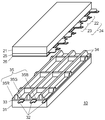
- FIG. 1 is an exploded perspective view showing a structure of a panel used in a plasma display device according to an embodiment of the present invention.
- FIG. 2 is an electrode array diagram of a panel used in the plasma display device according to one embodiment of the present invention.
- FIG. 3 is a diagram schematically showing a drive voltage waveform applied to each electrode of the panel used in the plasma display device according to one embodiment of the present invention.
- FIG. 4 is a waveform diagram schematically showing voltage waveforms applied to scan electrodes and data electrodes in one subfield in one embodiment of the present invention.
- FIG. 5 is a diagram illustrating an example of a method for simply measuring the discharge start voltage.
- FIG. 1 is an exploded perspective view showing a structure of a panel used in a plasma display device according to an embodiment of the present invention.
- FIG. 2 is an electrode array diagram of a panel used in the plasma display device according to one embodiment of the present invention.
- FIG. 3 is a diagram schematically showing a drive voltage waveform applied to each electrode of the
- FIG. 6A is a diagram schematically showing an example of a dither pattern used for dither processing in the plasma display apparatus according to one embodiment of the present invention.
- FIG. 6B is a diagram schematically showing another example of a dither pattern used for dither processing in the plasma display apparatus according to one embodiment of the present invention.
- FIG. 6C is a diagram schematically showing still another example of the dither pattern used for the dither processing in the plasma display device in accordance with the exemplary embodiment of the present invention.
- FIG. 7 is a circuit block diagram of the plasma display device according to one embodiment of the present invention.
- FIG. 8 is a diagram schematically showing an operation in the low luminance amplifier circuit of the plasma display device in accordance with the exemplary embodiment of the present invention.
- FIG. 10A is a diagram showing an example of the amplification factor for the input signal in the first correction in the embodiment of the present invention.
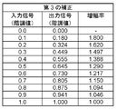
- FIG. 10B is a diagram showing an example of the amplification factor for the input signal in the second correction according to the embodiment of the present invention.
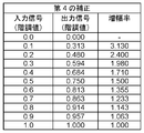
- FIG. 10C is a diagram showing an example of the amplification factor for the input signal in the third correction according to the embodiment of the present invention.
- FIG. 10D is a diagram showing an example of the amplification factor for the input signal in the fourth correction in the embodiment of the present invention.
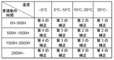
- FIG. 11 shows the temperature detected by the temperature detection circuit and the accumulated operation time measured by the accumulated operation time measurement circuit and the first correction, the second correction, the third correction, It is a figure which shows the relationship with correction
- FIG. 12 is a circuit diagram schematically showing a configuration of a scan electrode driving circuit of the plasma display device in accordance with the exemplary embodiment of the present invention.
- FIG. 13 is a circuit diagram schematically showing a configuration of a sustain electrode driving circuit of the plasma display device in accordance with the exemplary embodiment of the present invention.
- FIG. 14 is a circuit diagram schematically showing a configuration of a data electrode driving circuit of the plasma display device in accordance with the exemplary embodiment of the present invention.
- FIG. 1 is an exploded perspective view showing the structure of panel 10 used in the plasma display device according to one embodiment of the present invention.
- a plurality of display electrode pairs 24 each including a scanning electrode 22 and a sustaining electrode 23 are formed on a glass front substrate 21.
- a dielectric layer 25 is formed so as to cover the scan electrode 22 and the sustain electrode 23, and a protective layer 26 is formed on the dielectric layer 25.
- This protective layer 26 is made of a material using magnesium oxide (MgO) having high electron emission performance and excellent durability in order to easily generate discharge by lowering the discharge start voltage in the discharge cell.
- MgO magnesium oxide
- a plurality of data electrodes 32 are formed on the rear substrate 31, a dielectric layer 33 is formed so as to cover the data electrodes 32, and a grid-like partition wall 34 is formed thereon.
- a phosphor layer 35R that emits red (R)
- a phosphor layer 35G that emits green (G)
- a phosphor layer 35B that emits blue (B).
- the phosphor layer 35R, the phosphor layer 35G, and the phosphor layer 35B are collectively referred to as a phosphor layer 35.
- the red phosphor for example, a phosphor mainly composed of (Y, Gd) BO 3 : Eu is used, and as the green phosphor, for example, Zn 2 SiO 4 : Mn is mainly composed.
- a phosphor mainly composed of BaMgAl 10 O 17 : Eu is used as the blue phosphor.
- the phosphor forming the phosphor layer 35 is not limited to the above-described phosphor.
- the front substrate 21 and the rear substrate 31 are arranged to face each other so that the display electrode pair 24 and the data electrode 32 intersect with each other with a minute discharge space interposed therebetween. And the outer peripheral part is sealed with sealing materials, such as glass frit. Then, for example, a mixed gas of neon and xenon is sealed in the discharge space inside as a discharge gas.
- the discharge space is partitioned into a plurality of sections by partition walls 34, and discharge cells are formed at the intersections between the display electrode pairs 24 and the data electrodes 32.
- discharge is generated in these discharge cells, and the phosphor layer 35 of the discharge cells emits light (lights the discharge cells), thereby displaying a color image on the panel 10.
- One pixel is composed of three discharge cells that emit blue (B) light.
- the structure of the panel 10 is not limited to that described above.
- the rear substrate 31 may include a stripe-shaped partition wall.
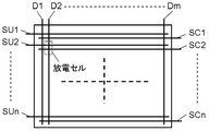
- FIG. 2 is an electrode array diagram of panel 10 used in the plasma display device according to one embodiment of the present invention.
- the panel 10 includes n scan electrodes SC1 to SCn (scan electrode 22 in FIG. 1) extended in the horizontal direction (row direction) and n sustain electrodes SU1 to SUn (sustain electrodes in FIG. 1). 23) are arranged, and m data electrodes D1 to Dm (data electrodes 32 in FIG. 1) extending in the vertical direction (column direction) are arranged.
- a green phosphor is applied as a phosphor layer 35G to a discharge cell having a blue color
- a blue phosphor is applied as a phosphor layer 35B to a discharge cell having a data electrode Dp + 2.
- the plasma display device in the present embodiment drives the panel 10 by the subfield method.
- the subfield method one field is divided into a plurality of subfields on the time axis, and a luminance weight is set for each subfield. Therefore, each field has a plurality of subfields.
- An image is displayed on the panel 10 by controlling light emission / non-light emission of each discharge cell for each subfield.
- the luminance weight represents a ratio of the luminance magnitudes displayed in each subfield, and the number of sustain pulses corresponding to the luminance weight is generated in the sustain period in each subfield. Therefore, for example, the subfield with the luminance weight “8” emits light with a luminance about eight times that of the subfield with the luminance weight “1”, and emits light with about four times the luminance of the subfield with the luminance weight “2”. Therefore, by selectively causing each subfield to emit light in a combination corresponding to an image signal, various gradations can be displayed on the panel 10 and an image can be displayed.
- each subfield has a write period, a sustain period, and an erase period.
- the forced initialization operation is not performed.
- the forced initializing operation is an initializing operation that forcibly generates an initializing discharge in a discharge cell regardless of whether or not there has been a discharge so far.
- a scan pulse is applied to the scan electrode 22 and an address pulse (data pulse) is selectively applied to the data electrode 32 to perform an address operation that selectively generates an address discharge in the discharge cells to emit light.
- an address pulse data pulse
- wall charges for generating a sustain discharge in the subsequent sustain period are formed in the discharge cell.
- the number of sustain pulses obtained by multiplying the luminance weight of each subfield by a predetermined proportional constant is alternately applied to the scan electrode 22 and the sustain electrode 23.
- This proportionality constant is the luminance magnification.
- the sustain pulse is applied to the scan electrode 22 and the sustain electrode 23 four times in the sustain period of the subfield having the luminance weight “2”. Therefore, the number of sustain pulses generated in the sustain period is 8.
- a sustain discharge is generated in the discharge cell that has generated the address discharge in the immediately preceding address period, and the discharge cell emits light.
- the operation of applying the sustain pulse to the discharge cell and emitting the discharge is the sustain operation.
- a subfield in which the sustain period is omitted may be provided in order to keep the emission luminance low.
- an erasing discharge is generated only in the discharge cells that have generated the address discharge in the address period of the subfield to which the erasing period belongs. Therefore, this erasing discharge is selectively generated only in the discharge cells that have generated the address discharge.
- this erasing discharge is generated, wall charges formed by the address discharge or the subsequent sustain discharge are erased, and wall charges necessary for the address discharge in the subsequent subfield are formed on each electrode.
- these operations are also referred to as “erase operations”.
- one field is divided into 10 subfields (SF1, SF2,..., SF10), and each subfield is (1, 2, 3, 6, 11, 18, 30). , 44, 60, 80).
- the number of subfields and the luminance weight of each subfield are not limited to the above values.
- the structure which switches the structure of a subfield based on an image signal etc. may be sufficient.
- FIG. 3 is a diagram schematically showing drive voltage waveforms applied to the respective electrodes of panel 10 used in the plasma display device according to one embodiment of the present invention.
- FIG. 3 shows scan electrode SC1 that performs the address operation first in the address period, scan electrode SCn that performs the address operation last in the address period, sustain electrode SU1 to sustain electrode SUn, and data electrode D1 to data electrode Dm.
- the drive voltage waveform to be applied is shown.
- Scan electrode SCi, sustain electrode SUi, and data electrode Dk in the following represent electrodes selected based on image data (data indicating light emission / non-light emission for each subfield) from among the electrodes.
- FIG. 3 mainly shows drive voltage waveforms in three subfields, that is, subfield SF1, subfield SF2, and subfield SF3.
- voltage 0 (V) is applied to data electrode D1 to data electrode Dm
- voltage Ve is applied to sustain electrode SU1 to sustain electrode SUn
- scan electrode SC1 to scan electrode SCn are applied to scan electrode SC1.
- a voltage Vc is applied.
- a scan pulse having a negative voltage Va is applied to the scan electrode SC1 in the first row where the address operation is first performed.
- an address pulse of a positive voltage Vd is applied to the data electrode Dk corresponding to the discharge cell that should emit light in the first row of the data electrodes D1 to Dm.
- the voltage difference at the intersection between the data electrode Dk of the discharge cell to which the address pulse of the voltage Vd is applied and the scan electrode SC1 is the difference between the externally applied voltage (voltage Vd ⁇ voltage Va) and the wall voltage on the data electrode Dk and the scan electrode.
- the difference from the wall voltage on SC1 is added.
- the voltage difference between data electrode Dk and scan electrode SC1 exceeds discharge start voltage VFds, and a discharge is generated between data electrode Dk and scan electrode SC1.
- the voltage difference between sustain electrode SU1 and scan electrode SC1 is the difference between the externally applied voltages (voltage Ve ⁇ voltage Va), and sustain electrode SU1.
- the difference between the upper wall voltage and the wall voltage on the scan electrode SC1 is added.
- the sustain electrode SU1 and the scan electrode SC1 are not easily discharged but are likely to be discharged. Can do.
- a discharge is generated between the sustain electrode SU1 and the scan electrode SC1 in a region intersecting the data electrode Dk, induced by a discharge generated between the data electrode Dk and the scan electrode SC1.
- address discharge is generated in the discharge cells (discharge cells to emit light) to which the scan pulse and address pulse are simultaneously applied.
- positive wall voltage is accumulated on scan electrode SC1
- negative wall voltage is accumulated on sustain electrode SU1
- negative wall voltage is also accumulated on data electrode Dk. Is done.
- the wall voltage on the electrode represents a voltage generated by wall charges accumulated on the dielectric layer 25 covering the electrode, the protective layer 26, the phosphor layer 35, and the like.
- a scan pulse is applied to the scan electrode SC2 in the second row, and an address pulse is applied to the data electrode Dk corresponding to the discharge cell to emit light in the second row.
- an address discharge is generated between data electrode Dk and scan electrode SC2 and between sustain electrode SU2 and scan electrode SC2, a positive wall voltage is accumulated on scan electrode SC2, and a negative voltage is applied on sustain electrode SU2. And a negative wall voltage is also accumulated on the data electrode Dk.
- the voltage at the intersection between the data electrode Dh and the scan electrode SC2 to which no address pulse is applied does not exceed the discharge start voltage VFds, no address discharge occurs. In this way, an address operation is performed in which an address discharge is generated in the discharge cells that should emit light in the second row, and a wall voltage is accumulated on each electrode.
- the same addressing operation is performed by scanning electrode SC3 in the third row, scanning electrode SC4 in the fourth row,..., Scanning electrode SC (n ⁇ 1) in the (n ⁇ 1) th row, scanning in the nth row.
- the process is sequentially performed from the discharge cell in the third row to the discharge cell in the nth row in the order of the electrode SCn, and the address period of the subfield SF1 is completed.
- the first voltage V1, the second voltage V2, and the third voltage V3 are defined as follows.
- FIG. 4 is a waveform diagram schematically showing voltage waveforms applied to scan electrode 22 and data electrode 32 in one subfield in one embodiment of the present invention.
- a voltage obtained by subtracting the voltage 0 (V)) is defined as a third voltage V3.
- the discharge start voltage VFds is the discharge start voltage in the address period in which the data electrode Dj is the anode and the scan electrode SCi is the cathode
- the discharge start voltage is the discharge start voltage in the sustain period in which the data electrode Dj is the cathode and the scan electrode SCi is the anode.
- the voltage is VFsd.
- the discharge with the data electrode Dj as the anode and the scan electrode SCi as the cathode is a discharge in which the electric field in the discharge cell when the discharge occurs is a high potential side on the data electrode Dj side and a low potential side on the scan electrode SCi side. It is.
- the discharge with the data electrode Dj as the cathode and the scan electrode SCi as the anode is a discharge in which the electric field in the discharge cell when the discharge occurs is a low potential side on the data electrode Dj side and a high potential side on the scan electrode SCi side. is there.
- the protective layer 26 of magnesium oxide having high electron emission performance is formed on the front substrate 21 with the scan electrode SCi, the discharge start voltage VFds is lower than the discharge start voltage VFsd.
- the voltage Va of the scan pulse applied to the scan electrode SCi is set so as to satisfy the following two conditions (condition 1) and (condition 2).
- a voltage obtained by subtracting the third voltage V3 from the second voltage V2 is a discharge start voltage VFds of discharge using the data electrode Dj as an anode and the scan electrode SCi as a cathode.
- the discharge start voltage VFsd of the discharge having the data electrode Dj as the cathode and the scan electrode SCi as the anode is, (V2 ⁇ V3) ⁇ (VFds + VFsd) It is.
- the voltage difference between the scan electrode SCi and the sustain electrode SUi causes the voltage Vs of the sustain pulse to be the wall voltage on the scan electrode SCi and the wall voltage on the sustain electrode SUi. The difference between and is added.
- the voltage difference between scan electrode SCi and sustain electrode SUi exceeds discharge start voltage VFss, and a sustain discharge is generated between scan electrode SCi and sustain electrode SUi.
- the fluorescent substance layer 35 light-emits with the ultraviolet-ray which generate
- negative wall voltage is accumulated on scan electrode SCi
- positive wall voltage is accumulated on sustain electrode SUi.
- a positive wall voltage is also accumulated on the data electrode Dk.
- sustain pulses of the number obtained by multiplying the luminance weight by a predetermined luminance magnification are alternately applied to scan electrode SC1 through scan electrode SCn and sustain electrode SU1 through sustain electrode SUn.
- the sustain discharge is continuously generated in the discharge cells in which the address discharge is generated in the address period.
- voltage 0 (V) is gradually increased from voltage 0 (V) to voltage Vr while voltage 0 (V) is applied to sustain electrode SU1 through sustain electrode SUn and data electrode D1 through data electrode Dm.
- An upward ramp waveform voltage is applied to scan electrode SC1 through scan electrode SCn.
- the charged particles generated by the erasing discharge are accumulated as wall charges on the sustain electrode SUi and the scan electrode SCi so as to alleviate the voltage difference between the sustain electrode SUi and the scan electrode SCi.
- the wall voltage on scan electrode SCi and sustain electrode SUi is weakened while the positive wall voltage on data electrode Dk remains. That is, unnecessary wall charges in the discharge cells are erased by the erase discharge.
- the voltage Vr is set to the same voltage value as the voltage Vs, but the voltage Vr may be a voltage value different from the voltage Vs.
- the voltage Vr is desirably set to an optimum voltage value according to the characteristics of the panel 10 and the specifications of the plasma display device.
- voltage Ve is applied to sustain electrode SU1 through sustain electrode SUn, and voltage 0 (V) is applied to data electrode D1 through data electrode Dm. Then, a downward ramp waveform voltage that gently falls from voltage 0 (V) to voltage Vi is applied to scan electrode SC1 through scan electrode SCn.
- the voltage Vi is set to be equal to or slightly higher than the voltage Va of the scanning pulse.
- This weak discharge discharges an excessive portion of the wall voltage on the scan electrode SCi, the wall voltage on the sustain electrode SUi, and the wall voltage on the data electrode Dk, and the wall voltage in the discharge cell
- the wall voltage is adjusted to a suitable level.
- erasing that selectively generates erasing discharges in the discharge cells that generated the sustaining discharge in the immediately preceding sustaining period (in the subfield in which the sustaining period is omitted, the discharge cell in which the addressing discharge occurred) Perform the action.
- an erasing discharge is generated only in the discharge cells in which the address discharge is generated in the address period of the subfield to which the erasing period belongs, and in the discharge cells in which the address discharge is not generated. Erase discharge does not occur. Accordingly, in a discharge cell displaying black (gradation value “0”) that does not generate a sustain discharge, neither an initializing discharge, an address discharge, a sustain discharge, nor an erasing discharge is generated. There is no light emission.
- each voltage value is desirably set optimally based on the discharge characteristics of panel 10 and the specifications of the plasma display device.
- the subfield configuration described above is merely an example in the present embodiment, and the present invention is not limited to this subfield configuration. It is desirable to optimally set the number of subfields constituting one field and the luminance weight of each subfield according to the characteristics of the panel and the specifications of the plasma display device.
- the wall voltage on each electrode is shown assuming a reference potential of wall voltage 0 (V) inside the discharge cell space.
- V wall voltage
- the discharge start voltage VFds and the discharge start voltage VFsd of the panel 10 used in the present embodiment are measured by the method described later, and their values are as follows.
- the discharge start voltage varies depending on the phosphor.
- the inventor of the present application measured the panel 10, and in the discharge cell coated with the red phosphor, the discharge start voltage VFds between the “data electrode 32 and the scan electrode 22” was 200 ⁇ 10 (V), and the discharge start voltage was The VFsd was 320 ⁇ 10 (V).
- the discharge start voltage VFds between “data electrode 32 and scan electrode 22” is 220 ⁇ 10 (V), and the discharge start voltage VFsd is 350 ⁇ 10 (V). there were.
- the discharge start voltage VFds between the “data electrode 32 and the scan electrode 22” is 200 ⁇ 10 (V), and the discharge start voltage VFsd is 330 ⁇ 10 (V). there were.
- the discharge start voltage VFss between the “scan electrode 22 and the sustain electrode 23” is 250 ⁇ 10 (V) in the discharge cell coated with the red phosphor and the discharge cell coated with the blue phosphor. It was 280 ⁇ 10 (V) in the discharge cell coated with the phosphor.
- the low-voltage side voltage of the sustain pulse is the voltage 0 (V)
- the voltage applied to the data electrode 32 during the sustain period is the voltage 0 (V)
- the first voltage V1 is the voltage 0. (V).
- the third voltage V3 is the voltage Va ( ⁇ 280 (V)).
- the discharge start voltage VFds is larger in the discharge cell coated with the green phosphor than the other discharge cells, and its maximum value is the voltage 230 (V) in consideration of variation.
- (Condition 1) is (first voltage V1 ⁇ third voltage V3) ⁇ VFds.
- (Maximum value of VFds) 230 (V) It is. That is, (First voltage V1 ⁇ third voltage V3)> (maximum value of VFds)
- (condition 1) is satisfied in all discharge cells.
- the second voltage V2 is the voltage Vs (200 (V)).
- the discharge start voltage VFsd is smaller in the discharge cell coated with the red phosphor than the other discharge cells, and its minimum value is the voltage 310 (V) in consideration of variation.
- the discharge start voltage VFds is smaller in discharge cells coated with red and blue phosphors than other discharge cells, and its minimum value is a voltage 190 (V) in consideration of variation. Therefore, the minimum value of the sum of the discharge start voltage VFsd and the discharge start voltage VFds is the voltage 500 (V).
- a voltage not lower than the voltage Va which is the low voltage side voltage of the scan pulse and not higher than the voltage Vs which is the high voltage side voltage of the sustain pulse is applied to the scan electrode 22.
- a voltage lower than the voltage Va that is the low-voltage side voltage of the scan pulse or a voltage that exceeds the voltage Vs that is the high-voltage side voltage of the sustain pulse is not applied to the scan electrode 22. Therefore, the discharge cells that did not generate the address discharge do not emit light.
- of the voltage Va which is the low-voltage side voltage of the scan pulse is the high-voltage side voltage of the sustain pulse. Is larger than the absolute value
- the drive voltage waveform applied to each electrode, in particular, the voltage Va of the scan pulse is set so as to satisfy (Condition 1) and (Condition 2).
- an erasing discharge is selectively generated only in the discharge cells that have generated the address discharge in the address period of the subfield to which the erasing period belongs.
- the voltage obtained by subtracting the third voltage V3 from the first voltage V1 is equal to or higher than the discharge start voltage VFds (Condition 1), and the second voltage V2 to the third voltage.
- the voltage obtained by subtracting V3 does not exceed the sum of the discharge start voltage VFds and the discharge start voltage VFsd (condition 2).
- address discharge is generated in the discharge cells that should generate address discharge, and address discharge is not generated in discharge cells that should not generate address discharge, even if forced initialization is not performed. Can do. That is, the write operation can be performed stably. The reason is considered as follows.
- the forced initialization operation is not performed in this embodiment. Therefore, in the discharge cell displaying black (gradation value “0”), neither an initializing discharge, an addressing discharge, a sustaining discharge, nor an erasing discharge is generated. Therefore, it is difficult to appropriately control the wall voltage, and the wall voltage of the discharge cell displaying black tends to be unstable.
- the wall voltage is slowly accumulated on the electrodes so as to alleviate the potential difference between the electrodes by the voltages applied to the scan electrodes SCi, the sustain electrodes SUi, and the data electrodes Dj. It will be done.
- the neglected wall voltage when the sustain pulse is alternately applied to the scan electrode SCi and the sustain electrode SUi is It is a voltage between the high voltage and the low voltage.
- the drive voltage waveform other than the sustain pulse is also applied to the discharge cell, it is considered that the neglected wall voltage of each discharge cell is substantially close to the low voltage of the sustain pulse.
- the neglected wall voltage is greatly affected by the charging characteristics of the phosphor applied inside the discharge cell.
- the charging characteristics of the phosphor are +20 ( ⁇ C / g) for the red phosphor, ⁇ 30 ( ⁇ C / g) for the green phosphor, and +10 ( ⁇ C) for the blue phosphor. / G).
- the leaving wall voltage of the discharge cell coated with the green phosphor is lower than that of the discharge cell coated with the red or blue phosphor. .
- the wall voltage is gradually accumulated on the data electrode Dh of the discharge cell displaying black without generating the address discharge, generally toward the low-voltage side voltage of the sustain pulse or the neglected wall voltage higher than that.
- the voltage Va of the scan pulse in the present embodiment is a voltage satisfying (Condition 1). Therefore, a positive wall voltage sufficient to generate the address discharge is accumulated on the data electrode Dh, and the address discharge can be generated in the discharge cells without performing any forced initialization operation.
- the wall voltage of the discharge cell displaying black gradually approaches the left wall voltage.
- a dark current current that flows in a state where no discharge occurs
- the voltage Va of the scan pulse in the address period is particularly (Condition 1).
- the wall voltage necessary for the address discharge can be accumulated in the discharge cell without performing the forced initialization operation before the address period.
- a dark current that plays the role of priming particles for stably generating the address discharge can be generated in the discharge cell.
- each voltage must be set so that the voltage between the “data electrode 32 and the scan electrode 22” becomes equal to or lower than the discharge start voltage VFsd when the sustain pulse voltage Vs is applied. I must. This condition is (Condition 2).
- the drive voltage waveform is set so as to satisfy (Condition 1) and (Condition 2) in all the discharge cells. Therefore, the address discharge can be stably generated even if the forced initialization operation is omitted. As a result, it is possible to display an image without causing light emission not related to gradation display.
- an erase discharge is generated only in the discharge cells in which the address discharge is generated in the address period of the subfield to which the erase period belongs, and the discharge in which the address discharge is not generated. Erase discharge does not occur in the cell. Accordingly, in a discharge cell displaying black (gradation value “0”) that does not generate a sustain discharge, neither an initializing discharge, an address discharge, a sustain discharge, nor an erasing discharge is generated. There is no light emission.
- a stable writing operation can be performed without performing a forced initialization operation, black luminance can be suppressed, and an image with high contrast can be displayed on the panel 10.
- the slope of the rising ramp waveform voltage applied to scan electrode SC1 through scan electrode SCn in the erasing period is 10 (V / ⁇ sec), and the slope of the falling ramp waveform voltage is ⁇ 1.5 (V / ⁇ sec).
- this numerical value is only one example when generating an up-slope waveform voltage and a down-slope waveform voltage, and the present invention does not limit the slope of the up-slope waveform voltage and the down-slope waveform voltage to these values. Absent.
- a weak erasing discharge is repeatedly generated a plurality of times during the erasing period without using the forced initialization operation, and a weak erasing discharge is repeatedly generated several times. Since the wall voltage can be accumulated in the discharge cell and the priming particles can be generated, the address discharge can be stably generated in the subsequent address period.
- discharge start voltage VFsd the discharge start voltage VFds
- the wall voltage can be easily measured, for example, by the method described below.
- FIG. 5 is a diagram showing an example of a method for simply measuring the discharge start voltage.
- the wall charge is erased. Specifically, as shown in the wall charge erasing period of FIG. 5, a pulse voltage Vers sufficiently higher than the expected discharge start voltage is alternately applied between the electrodes to be measured, for example, the data electrode 32 and the scan electrode 22. Apply to.
- a pulsed voltage Vmsr lower than the expected discharge start voltage is applied to one electrode (for example, the data electrode 32). Then, light emission due to the discharge at that time is detected by using a light detection sensor such as a photomultiplier.
- the minimum value of the absolute value of the voltage Vmsr when light emission is observed in the measurement period is the discharge start voltage.
- the discharge start voltage VFds of the discharge with the data electrode 32 as the anode and the scan electrode 22 as the cathode can be measured. Further, when the voltage Vmsr applied in the measurement period is a negative voltage, the discharge start voltage VFsd of the discharge having the data electrode 32 as a cathode and the scan electrode 22 as an anode can be measured.
- the discharge start voltage is known, the voltage at which discharge starts is measured for the discharge cell in which the wall voltage is accumulated, and the wall voltage can be known as the difference between the voltage value and the discharge start voltage measured in advance. .
- the discharge start voltage VFsd, the discharge start voltage VFds, and the wall voltage can be obtained from IEEE TRANSACTIONS ON ELECTRON DEVICES, VOL. ED-24, NO. 7, JULY, 1977 “Measurement of a Plasma in the AC Plasma Display panel Usage RF Capacitance and Microwave Techniques”, etc.
- an image is displayed on panel 10 using a subfield method.
- the subfield method one field is composed of a plurality of subfields whose luminance weights are determined in advance, and a subfield that emits light is selected according to the magnitude of the gradation value to be displayed.
- the address operation is not performed in all the subfields from the subfield SF1 to the subfield SF10.
- the sustain discharge never occurs in the discharge cell, and the gradation value “0” having the lowest luminance is displayed.
- the address operation is performed only in the subfield SF1 that is the subfield having the luminance weight “1”, and the address operation is not performed in the other subfields.
- the number of sustain discharges corresponding to the luminance weight “1” is generated in the discharge cell, and light emission with brightness corresponding to the gradation value “1” is generated, and the gradation value “1” is displayed.
- the write operation is performed, and the write operation is not performed in the other subfields.
- the number of sustain discharges corresponding to the luminance weight “9” is generated in the discharge cell, and the light emission having the brightness corresponding to the gradation value “9” is generated to display the gradation value “9”.
- each subfield generates a sustain pulse as many times as the luminance weight and emits light according to the gradation value to be displayed. Select. By doing so, each discharge cell generates sustain discharges the number of times corresponding to the gradation value to be displayed, causes the discharge cell to emit light with the luminance corresponding to the gradation value, and displays an image on the panel 10. .
- the gradation value that can be displayed on the panel 10 does not continuously change from the minimum gradation value to the maximum gradation value.
- the gradation values that can be displayed on the panel 10 change discretely, and the amount of change is additive.
- the minimum value when increasing the gradation value is the gradation value “1”
- the gradation value that can be displayed on the panel 10 is from the minimum value to the maximum value of the gradation value.
- Gradation value “1” such as gradation value “0”, gradation value “1”, gradation value “2”,..., Gradation value “255”. Increase by increments.
- the brightness perceived by humans changes logarithmically with changes in luminance, as is generally known. Therefore, for example, when the gradation value is changed from the minimum value to the maximum value that can be displayed on the panel 10, the gradation value is changed at equal intervals (for example, the gradation value). Despite being changed by “1”, a person observing the change in the brightness of the panel 10 does not perceive that the brightness is changing at equal intervals. For humans observing changes in the brightness of the panel 10, the brightness changes more greatly when the gradation value is small than when the gradation value is large. Perceived as.
- the gradation display capability (ability to display an image smoothly) when displaying a dark image is reduced.
- an intermediate gradation value can be displayed in a pseudo manner by performing dither processing or error diffusion processing on the image signal, and the gradation value that can be displayed on the panel 10. Has increased. Thereby, the gradation display capability in the plasma display device is improved, and a smoother image can be displayed.
- the gradation value “0” is black, and is a gradation value that does not emit light (emission by sustain discharge) in all subfields.
- the gradation value “1” is a gradation value in which only the subfield with the smallest luminance weight (for example, subfield SF1) emits light and the other subfields do not emit light. Therefore, the gradation value between the gradation value “0” and the gradation value “1” cannot be displayed on the panel 10 without performing the dither process (or error diffusion process).
- the gradation value “0” is based on a predetermined dither pattern.
- the dither processing is performed by arranging the discharge cells displaying "" and the discharge cells displaying the gradation value "1".
- black wrinkles represent discharge cells that display a gradation value “0”, and white wrinkles represent discharge cells that display a gradation value “1”.
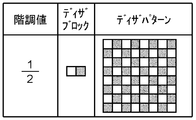
- FIG. 6A is a diagram schematically showing an example of a dither pattern used for dither processing in the plasma display device according to one embodiment of the present invention.
- FIG. 6A shows an example of a dither pattern when the minimum value of the intermediate gradation value is the gradation value “1/2”.
- the dither block which is the minimum block constituting the dither pattern, is composed of two discharge cells.
- the discharge cell displaying the gradation value “0” and the discharge cell displaying the gradation value “1” are adjacent to each other.
- the discharge cells are not actually adjacent.
- a discharge cell displaying a gradation value “0” and a discharge cell displaying a gradation value “1” for a blue discharge cell are based on a dither pattern.
- a dither pattern Arrange. The same applies to the gradation values of other colors, and the same applies to the other dither patterns shown below.
- the discharge cells displaying the gradation value “0” and the discharge cells displaying the gradation value “1” are generated at a ratio of 1: 1.
- a dither pattern (checkered dither pattern) is generated in which discharge cells displaying the gradation value “0” and discharge cells displaying the gradation value “1” are arranged in a checkered pattern at a ratio of 1: 1.
- the gradation value “1/2” can be displayed on the panel 10 in a pseudo manner.
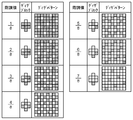
- FIG. 6B is a diagram schematically showing another example of a dither pattern used for dither processing in the plasma display device according to one embodiment of the present invention.
- the minimum value of the intermediate gradation value is the gradation value “1/4”, the gradation value “1/4”, the gradation value “2/4”, and the gradation value “3/4”.
- An example of a dither pattern when each gradation value is displayed on the panel 10 is shown.
- the dither block which is the smallest block constituting the dither pattern, is composed of four discharge cells.
- the discharge cell displaying the gradation value “0” and the gradation value “1” are displayed.
- the discharge cells to be displayed are generated at a ratio of 3: 1.
- a dither pattern in which the discharge cells displaying the gradation value “0” and the discharge cells displaying the gradation value “1” are arranged at a ratio of 3: 1 can be generated.
- the tone value “1/4” can be displayed on the panel 10.
- the discharge cells displaying the gradation value “0” and the discharge cells displaying the gradation value “1” are generated at a ratio of 2: 2.
- a dither pattern (checkered dither pattern) is generated in which discharge cells displaying gradation value “0” and discharge cells displaying gradation value “1” are arranged in a checkered pattern at a ratio of 2: 2.
- the gradation value “2/4” can be displayed on the panel 10 in a pseudo manner.
- the discharge cells displaying the gradation value “0” and the discharge cells displaying the gradation value “1” are generated at a ratio of 1: 3.
- a dither pattern in which the discharge cells displaying the gradation value “0” and the discharge cells displaying the gradation value “1” are arranged at a ratio of 1: 3 can be generated.
- the tone value “3/4” can be displayed on the panel 10.
- FIG. 6C is a diagram schematically showing still another example of the dither pattern used for the dither process in the plasma display device according to the embodiment of the present invention.
- the minimum value of the intermediate gradation value is the gradation value “1/8”, the gradation value “1/8”, the gradation value “2/8”, the gradation value “3/8”,
- the dither pattern for displaying the gradation value “4/8”, gradation value “5/8”, gradation value “6/8”, gradation value “7/8” on the panel 10 An example is shown.
- the dither block which is the minimum block constituting the dither pattern, is composed of eight discharge cells. However, in this case, the discharge cells are not arranged in 2 rows and 4 columns or 4 rows and 2 columns, but the discharge cells are arranged in a “+” shape to form a dither block.
- the discharge cell displaying the gradation value “0” and the gradation value “1” are displayed.
- the discharge cells to be displayed are generated at a ratio of 7: 1.
- a dither pattern can be generated in which the discharge cells displaying the gradation value “0” and the discharge cells displaying the gradation value “1” are arranged at a ratio of 7: 1.
- the tone value “1/8” can be displayed on the panel 10.
- the discharge cells displaying the gradation value “0” and the discharge cells displaying the gradation value “1” are generated at a ratio of 6: 2.
- a dither pattern in which the discharge cells displaying the gradation value “0” and the discharge cells displaying the gradation value “1” are arranged at a ratio of 6: 2 can be generated.
- the tone value “2/8” can be displayed on the panel 10.
- the discharge cells displaying the gradation value “0” and the discharge cells displaying the gradation value “1” are generated at a ratio of 5: 3.
- a dither pattern can be generated in which the discharge cells displaying the gradation value “0” and the discharge cells displaying the gradation value “1” are arranged at a ratio of 5: 3.
- the tone value “3/8” can be displayed on the panel 10.
- the discharge cells displaying the gradation value “0” and the discharge cells displaying the gradation value “1” are generated at a ratio of 4: 4.
- a dither pattern (checkered dither pattern) is generated in which the discharge cells displaying the gradation value “0” and the discharge cells displaying the gradation value “1” are arranged in a checkered pattern at a ratio of 4: 4.
- the pseudo gradation value “4/8” can be displayed on the panel 10.
- the discharge cells displaying the gradation value “0” and the discharge cells displaying the gradation value “1” are generated at a ratio of 3: 5.
- a dither pattern in which the discharge cells displaying the gradation value “0” and the discharge cells displaying the gradation value “1” are arranged at a ratio of 3: 5 can be generated.
- the tone value “5/8” can be displayed on the panel 10.
- discharge cells displaying the gradation value “0” and discharge cells displaying the gradation value “1” are generated at a ratio of 2: 6.
- a dither pattern in which the discharge cells displaying the gradation value “0” and the discharge cells displaying the gradation value “1” are arranged at a ratio of 2: 6 can be generated.
- the tone value “6/8” can be displayed on the panel 10.
- the discharge cells displaying the gradation value “0” and the discharge cells displaying the gradation value “1” are generated at a ratio of 1: 7.
- a dither pattern in which the discharge cells displaying the gradation value “0” and the discharge cells displaying the gradation value “1” are arranged at a ratio of 1: 7 can be generated.
- the tone value “7/8” can be displayed on the panel 10.
- the gradation value “a” and the gradation value “b” are equally divided into N, and (N ⁇ 1) intermediate gradations between the gradation value “a” and the gradation value “b”.
- the dither block is composed of N discharge cells.
- the discharge cells may be arranged so that the dither block has a square shape.
- the discharge cells are arranged so as to have a non-rectangular shape. May be. Note that a is an integer greater than or equal to “0”, b is an integer greater than or equal to “1”, and N is an integer greater than or equal to “2”.
- n is an integer of 1 or more and less than N.
- the dither block is composed of four discharge cells.
- the gradation value “5” is displayed in one discharge cell of the dither block, and the remaining three
- the gradation value “6” is displayed in the discharge cell.
- the dither block is generated so that no gap is generated in the area of the panel 10 where the gradation value “5.25” is displayed and no overlap occurs. In this way, the gradation value “5.25” can be displayed on the panel 10 in a pseudo manner.
- FIG. 7 is a circuit block diagram of the plasma display device 40 in one embodiment of the present invention.
- the plasma display apparatus 40 uses a panel 10 having a plurality of discharge cells each having a scan electrode 22, a sustain electrode 23, and a data electrode 32, and a single field using a plurality of subfields having an address period, a sustain period, and an erase period. And a drive circuit that generates the drive voltage waveform shown in FIGS. 3 and 4 and applies it to each electrode of the panel 10 to drive the panel 10.
- the drive circuit is necessary for the image signal processing circuit 41, the data electrode drive circuit 42, the scan electrode drive circuit 43, the sustain electrode drive circuit 44, the timing generation circuit 45, the temperature detection circuit 96, the cumulative operation time measurement circuit 98, and each circuit block.
- a power supply circuit (not shown) for supplying a proper power supply is provided.
- the temperature detection circuit 96 includes a temperature sensor 97 made of a generally known element such as a thermocouple used for detecting the temperature, and detects the temperature of the panel 10. Then, the temperature of the panel 10 detected by the temperature sensor 97 is compared with a plurality of predetermined temperature thresholds to determine what the temperature of the panel 10 is, and the result is subjected to image signal processing. Output to the circuit 41. Specifically, the temperature threshold is set to 5 ° C., 10 ° C., 20 ° C., and the panel temperature is lower than 5 ° C., 5 ° C. or higher, lower than 10 ° C. And a signal indicating the result is output to the image signal processing circuit 41 (low luminance amplification circuit 46).
- a temperature threshold is set to 5 ° C., 10 ° C., 20 ° C.
- the panel temperature is lower than 5 ° C., 5 ° C. or higher, lower than 10 ° C.
- a signal indicating the result is output to the image
- the accumulated operation time measuring circuit 98 has a generally known timer 99 having an integration function in which a numerical value increases by a certain amount per unit time during an energization period of the panel 10 (during the operation period of the panel 10).
- the measurement time is accumulated without being reset. That is, even when the power of the plasma display device 40 is turned off, the measurement time is not reset and the measurement time immediately before the power is turned off is held in the timer 99, and the plasma display device 40 is turned on again.
- the operation time of the plasma display device 40 is measured by the timer 99 following the measurement time up to the previous time.
- the accumulated operation time measuring circuit 98 can measure the accumulated operation time (accumulated operation time) of the plasma display device 40 after the plasma display device 40 starts the operation for the first time. That is, the cumulative operation time measuring circuit 98 measures the cumulative operation time of the panel 10.
- the cumulative operation time measuring circuit 98 compares the cumulative operation time of the panel 10 measured by the timer 99 with a plurality of predetermined cumulative time thresholds to determine whether or not the cumulative operation time of the panel 10 has exceeded a predetermined time.
- a signal representing the result of the determination is output to the image signal processing circuit 41.
- 500 hours, 1000 hours, and 2000 hours are set as the cumulative time threshold, and the cumulative operation time is less than 500 hours, 500 hours or more and less than 1000 hours, 1000 hours or more and less than 2000 hours, or 2000 hours. Whether it is the above or not is determined, and a signal indicating the result is output to the image signal processing circuit 41 (low luminance amplification circuit 46).
- each of the above-described threshold values is merely an example in the present embodiment, and the present invention is not limited to the above-described numerical values.
- Each threshold value is desirably set to an optimum value based on the characteristics of the panel 10 and the specifications of the plasma display device 40.
- the image signal processing circuit 41 includes a low luminance amplification circuit 46, a dither processing circuit 47, and a subfield conversion circuit 48.
- the low luminance amplifying circuit 46 converts each of the input image signals of the red primary color signal sigR, the green primary color signal sigG, and the blue primary color signal sigB (hereinafter simply referred to as “image signal”) of the image signal. Amplification is performed at an amplification factor corresponding to the magnitude and the temperature detected by the temperature detection circuit 96 and the cumulative operation time measured by the cumulative operation time measurement circuit 98. Although details will be described later, in this embodiment, the amplification factor is non-linear, and the low luminance amplifier circuit 46 outputs an image signal having a signal level (signal magnitude) less than the gradation value “1”.
- Amplification is performed with an amplification factor larger than the amplification factor of an image signal equal to or higher than the signal level corresponding to the gradation value “1”.
- an image signal having a signal level corresponding to the gradation value “1” is simply referred to as an “image signal having a gradation value“ 1 ””.
- the discharge cell displaying the gradation value “1” only the subfield with the smallest luminance weight (for example, subfield SF1) emits light, and the other subfields do not emit light.
- the correction performed in the low luminance amplifier circuit 46 is to amplify the input signal at an amplification factor corresponding to the probability of occurrence of a defective discharge and output it to compensate for a decrease in luminance caused by the defective discharge. This is not a correction such as contrast adjustment or brightness adjustment that is generally performed to improve the brightness of the display image.
- the dither processing circuit 47 sets a gradation value for each discharge cell based on the image signal output from the low luminance amplification circuit 46 and the luminance weight assigned to each subfield.
- the image signals input to the dither processing circuit 47 are a red primary color signal sigR, a green primary color signal sigG, and a blue primary color signal sigB.
- the dither processing circuit 47 converts the primary color signal sigR, the primary color signal sigG, and the primary color signal sigB.
- First, R, G, and B gradation values (gradation values expressed in one field) are set in each discharge cell.
- dither processing using the above-described dither pattern or the like is performed.
- the dither processing can be realized, for example, using a circuit described in JP-A-2004-138383.
- the subfield conversion circuit 48 converts the signal (grayscale value) output from the dither processing circuit 47 into image data indicating light emission / non-light emission for each subfield (light emission / non-light emission is a digital signal “1”, “0 ”). That is, the subfield conversion circuit 48 converts the image signal for each field (gradation value based on the image signal) into image data indicating light emission / non-light emission for each subfield.
- the subfield conversion circuit 48 can be configured using, for example, a semiconductor memory device that stores a conversion table in which gradation values and image data are associated with each other.
- the image signal processing circuit 41 does not input a primary color image signal but a luminance signal (Y signal) and a saturation signal (C signal, or RY signal and BY signal, or u signal, and u signal). 7), the primary color signal sigR, the primary color signal sigG, and the primary color signal sigB are calculated based on the luminance signal and the saturation signal (a circuit block for calculating the primary color signal based on the luminance signal and the saturation signal is shown in FIG. 7). The calculated primary color signal is input to the low luminance amplification circuit 46.
- the timing generation circuit 45 forms a single field using a plurality of subfields having a write period, a sustain period, and an erase period based on the horizontal synchronization signal and the vertical synchronization signal, and controls various operations of each circuit block. Generate timing signals.
- the generated timing signal is supplied to each circuit block (data electrode drive circuit 42, scan electrode drive circuit 43, sustain electrode drive circuit 44, image signal processing circuit 41, etc.).
- Scan electrode drive circuit 43 includes a ramp waveform voltage generation circuit, a sustain pulse generation circuit, and a scan pulse generation circuit (not shown in FIG. 7) so as to satisfy the above-described two conditions (condition 1) and (condition 2).
- the drive voltage waveforms shown in FIGS. 3 and 4 are generated based on the timing signal supplied from the timing generation circuit 45 and applied to each of the scan electrodes SC1 to SCn.
- the ramp waveform voltage generating circuit generates a descending ramp waveform voltage to be applied to scan electrode SC1 through scan electrode SCn based on the timing signal during the erase period.
- the sustain pulse generating circuit generates a sustain pulse to be applied to scan electrode SC1 through scan electrode SCn based on the timing signal during the sustain period.
- the scan pulse generating circuit includes a plurality of scan electrode driving ICs (scan ICs), and generates scan pulses to be applied to scan electrode SC1 through scan electrode SCn based on a timing signal during an address period.
- Sustain electrode drive circuit 44 includes a sustain pulse generation circuit and a circuit for generating voltage Ve (not shown in FIG. 7), and the drive voltage shown in FIG. 3 based on the timing signal supplied from timing generation circuit 45.
- a waveform is created and applied to each of sustain electrode SU1 through sustain electrode SUn.
- a sustain pulse is generated based on the timing signal
- voltage Ve is generated based on the timing signal and applied to sustain electrode SU1 through sustain electrode SUn.
- the data electrode drive circuit 42 converts the data for each subfield constituting the image data based on the image signal into signals corresponding to the data electrodes D1 to Dm. Then, based on the signal and the timing signal supplied from the timing generation circuit 45, the data electrodes D1 to Dm are driven. In the address period, an address pulse is generated and applied to each of the data electrodes D1 to Dm.
- FIG. 8 is a diagram schematically showing an operation in the low luminance amplification circuit 46 of the plasma display device 40 in one embodiment of the present invention.
- FIG. 9 is an enlarged view showing a part of the operation of the low luminance amplifier circuit 46 of the plasma display device 40 according to the embodiment of the present invention.
- FIG. 9 is an enlarged view of a part of FIG. 8, that is, an operation when the input image signal is equal to or lower than the gradation value “1” (region surrounded by a circle in FIG. 8).
- the horizontal axis indicates the magnitude of an image signal (hereinafter simply referred to as “input signal”) input to the low luminance amplifier circuit 46, and the vertical axis indicates the image signal output by the low luminance amplifier circuit 46. (Hereinafter simply referred to as “output signal”). However, in FIG. 8 and FIG. 9, each of the input signal and the output signal is converted into a gradation value.
- the low luminance amplifier circuit 46 sets the amplification factor to “1” when the signal level (signal magnitude) of the input signal is equal to or higher than the gradation value “1”.
- the output signal is output as the input signal without changing the magnitude of the input signal.
- the low luminance amplification circuit 46 sets the amplification factor to a numerical value of “1” or more, and outputs as output signal ⁇ input signal.
- the amplification factor when the signal level of the input signal is less than the gradation value “1” is not maintained at a constant magnitude.
- the low luminance amplification circuit 46 sets the amplification factor relatively large when the signal level of the input signal is close to the gradation value “0”, and gradually increases the amplification factor from the gradation value “0” to the gradation value “1”.
- the gain is changed according to the signal level of the input signal (except for the first correction described later) so that the gain becomes “1” when the gradation value is “1”. Therefore, the magnitude of the output signal changes nonlinearly with respect to the magnitude of the input signal (except for the first correction).
- the low-brightness amplification circuit 46 uses the temperature detected by the temperature detection circuit 96 and the accumulated operation time measurement circuit to calculate the amplification factor when the signal level of the input signal is less than the gradation value “1”. The operation is changed based on the accumulated operation time measured in 98, and details of this operation will be described later.
- the low-brightness amplification circuit 46 is different from, for example, the first correction, the second correction, the third correction, and the fourth correction.
- the input signal is amplified using any one of the amplification factors. As shown in FIG. 9, the amplification factor of each correction has the largest fourth correction, the third correction next, and the second correction next.
- the first correction has the smallest amplification factor, and the amplification factor is “1”.
- FIG. 10A is a diagram illustrating an example of an amplification factor for an input signal in the first correction according to the embodiment of the present invention.
- FIG. 10B is a diagram showing an example of the amplification factor for the input signal in the second correction according to the embodiment of the present invention.
- FIG. 10C is a diagram showing an example of the amplification factor for the input signal in the third correction according to the embodiment of the present invention.
- FIG. 10D is a diagram showing an example of the amplification factor for the input signal in the fourth correction in the embodiment of the present invention.
- the input signal and the output signal are respectively converted into gradation values.
- the amplification factor is set to “1”. Accordingly, when the first correction is applied to the input signal in the low luminance amplifier circuit 46, the magnitude of the output signal is equal to the magnitude of the input signal, as shown in FIG. 10A.
- the amplification factor is set larger than that in the first correction.
- the amplification factor when the second correction is applied to the input signal in the low luminance amplifier circuit 46 is “1.370” when the gradation value of the input signal is “0.1”. ”.
- the amplification factor when the gradation value of the input signal is“ 0.2 ”is“ 1.270 ”, and the amplification factor when the gradation value of the input signal is“ 0.3 ”is“ 1 ”. .237 ”, the amplification factor when the gradation value of the input signal is“ 0.4 ”is“ 1.200 ”, and the amplification factor when the gradation value of the input signal is“ 0.5 ”.
- the amplification factor is “1.120” when the gradation value of the input signal is “0.6”, and the amplification factor when the gradation value of the input signal is “0.7”.
- the rate is “1.083”, the amplification factor is “1.055” when the tone value of the input signal is “0.8”, and the tone value of the input signal is “0.9”
- the second correction is used in the low luminance amplifier circuit 46, as shown in FIG. 10B, for example, if the gradation value of the input signal is “0.1”, the gradation value of the output signal is “0.1”. If the gradation value of the input signal is “0.5”, the gradation value of the output signal is “0.578”, and the gradation value of the input signal is “0.9”. In this case, the gradation value of the output signal is “0.926”.
- the amplification factor is set larger than that in the second correction.
- the amplification factor when the third correction is applied to the input signal in the low luminance amplifier circuit 46 is “1.800” when the gradation value of the input signal is “0.1”. ”.
- the amplification factor when the gradation value of the input signal is“ 0.2 ”is“ 1.620 ”, and the amplification factor when the gradation value of the input signal is“ 0.3 ”is“ 1 ”. .497 ”, the amplification factor when the gradation value of the input signal is“ 0.4 ”is“ 1.388 ”, and the amplification factor when the gradation value of the input signal is“ 0.5 ”.
- the amplification factor is “1.217” when the gradation value of the input signal is “0.6”, and the amplification factor when the gradation value of the input signal is “0.7”.
- the rate is “1.150”
- the amplification factor is “1.094” when the gradation value of the input signal is “0.8”
- the gradation value of the input signal is “0.9”
- the third correction is used in the low luminance amplifier circuit 46, as shown in FIG. 10C, for example, if the gradation value of the input signal is “0.1”, the gradation value of the output signal is “0.1”. If the gradation value of the input signal is “0.5”, the gradation value of the output signal is “0.645”, and the gradation value of the input signal is “0.9”. In this case, the gradation value of the output signal is “0.941”.
- the amplification factor is set larger than that in the third correction.
- the amplification factor when the fourth correction is applied to the input signal in the low luminance amplifier circuit 46 is “3.130” when the gradation value of the input signal is “0.1”.
- the amplification factor when the gradation value of the input signal is “0.2” is “2.400”, and the amplification factor when the gradation value of the input signal is “0.3” is “1”. .980 ”, the amplification factor when the gradation value of the input signal is“ 0.4 ”is“ 1.710 ”, and the amplification factor when the gradation value of the input signal is“ 0.5 ”.
- the amplification factor when the gradation value of the input signal is “0.6” is “1.355”, and the amplification factor when the gradation value of the input signal is “0.7”
- the rate is “1.233”
- the amplification factor when the gradation value of the input signal is “0.8” is “1.143”
- the gradation value of the input signal is “0.9”
- the fourth correction is used in the low luminance amplifier circuit 46, as shown in FIG. 10D, for example, if the gradation value of the input signal is “0.1”, the gradation value of the output signal is “0.1”. If the gradation value of the input signal is “0.5”, the gradation value of the output signal is “0.750” and the gradation value of the input signal is “0.9”. In this case, the gradation value of the output signal is “0.957”.
- an input image signal having a predetermined magnitude less than the gradation value “1” is converted to the gradation value “
- the input image signal is amplified with an amplification factor larger than that of the input image signal of “1” or more, and the amplification factor of the input image signal less than the gradation value “1” is increased as the input image signal becomes smaller (except for the first correction). ).
- the low luminance amplifier circuit 46 in the present embodiment is configured to perform the first correction, the second correction, based on the temperature detected by the temperature detection circuit 96 and the accumulated operation time measured by the accumulated operation time measurement circuit 98. Either the third correction or the fourth correction is selected to amplify the input signal.
- FIG. 11 shows the temperature detected by the temperature detection circuit 96 and the cumulative operation time measured by the cumulative operation time measurement circuit 98 and the first correction, the second correction, and the third correction in the embodiment of the present invention.
- FIG. 10 is a diagram schematically showing a relationship with a fourth correction.
- the temperature detected by the temperature detection circuit 96 and the accumulated operation time measurement circuit 98 are selected from the first correction, the second correction, the third correction, and the fourth correction in the low luminance amplifier circuit 46.
- FIG. 6 schematically shows a selection method when selecting based on the accumulated operation time measured in FIG.
- the vertical cells represent changes in the accumulated operation time (hereinafter simply referred to as “accumulated operation time”) measured by the accumulated operation time measurement circuit 98, and the horizontal cells are detected by the temperature detection circuit 96. Represents the change in temperature.
- the low luminance amplification circuit 46 in the present embodiment selects the fourth correction regardless of the accumulated operation time.
- the low luminance amplifier circuit 46 selects the third correction if the cumulative operation time is less than 2000 hours, and the cumulative operation time is If it is 2000 hours or longer, the fourth correction is selected.
- the low luminance amplifier circuit 46 selects the second correction if the cumulative operation time is less than 1000 hours, and the cumulative operation time. If 1000 hours or more and less than 2000 hours, the third correction is selected, and if the cumulative operation time is 2000 hours or more, the fourth correction is selected.
- the low luminance amplifier circuit 46 selects the first correction if the cumulative operation time is less than 500 hours, and the cumulative operation time is 500 hours or more. If the accumulated operation time is 1000 hours or less and less than 2000 hours, the third correction is selected. If the accumulated operation time is 2000 hours or more, the fourth correction is selected. select.
- the low luminance amplifier circuit 46 when the temperature detected by the temperature detection circuit 96 is lower than the preset temperature threshold value, the low luminance amplifier circuit 46 according to the present embodiment is when the detected temperature is equal to or higher than the temperature threshold value. Rather, the amplification factor relating to the input image signal having the gradation value less than “1” is increased.
- the low luminance amplifier circuit 46 in the present embodiment has a cumulative operation time less than the cumulative time threshold when the cumulative operation time measured by the cumulative operation time measurement circuit 98 is equal to or greater than a preset cumulative time threshold.
- the amplification factor for the input image signal with the gradation value less than “1” is increased compared to
- the gradation value is assigned to the panel 10 using the above-described dither processing (or error diffusion processing) or the like. Is displayed in a pseudo manner.
- discharge failure the probability that the address discharge does not occur normally in the discharge cell (hereinafter also referred to as “discharge failure”) depends on the amount of priming particles present in the discharge cell, and the priming particles are insufficient. The probability of occurrence of defective discharge increases.
- Priming particles are generated in the discharge cell by the initialization discharge or the sustain discharge.
- the plasma display device 40 in the present embodiment does not perform the forced initialization operation. Therefore, in panel 10, the chance of generating priming particles decreases as the discharge cell generates a sustain discharge less frequently. Therefore, in a discharge cell having a large number of fields that do not emit light, the priming particles generated by the sustain discharge are likely to be insufficient, and the probability of occurrence of a discharge failure increases.
- the frequency of occurrence of the light-emitting field depends on the magnitude of the gradation value.
- the discharge cell that displays the image signal has a low frequency of light emission, and the light emission field.
- the number of non-light-emitting fields generated from one to the next light-emitting field is relatively increased. Therefore, in the discharge cell, priming particles are likely to be insufficient, and the probability of occurrence of a discharge failure is relatively high.
- the discharge cell displaying the image signal has a higher frequency of occurrence of a light emitting field and emits light.
- the number of non-light emitting fields that occur between the field and the next light emitting field is relatively reduced. Therefore, in the discharge cell, since the priming particles are relatively increased, the probability of occurrence of a discharge failure is relatively low.
- the gradation value to be displayed is compensated in advance for the gradation value to be displayed in the panel 10 by compensating for the luminance reduced by the discharge failure in advance. It is possible to display.
- the amplification factor is set to a numerical value of “1” or more, and the output signal ⁇ the input signal is output for this reason. This is because the gradation value to be displayed is pseudo-displayed on the panel 10 with the correct gradation value.
- the tone value is slightly larger than “0.5”. Therefore, it is desirable to set the amplification factor in consideration of these points.
- the temperature of the panel 10 is one factor that increases the probability that a discharge failure will occur in the discharge cell.
- initial electrons that cause discharge in the discharge cell are released from magnesium oxide used in the protective layer 26.
- the amount of initial electrons generated in the discharge cell depends on the temperature of magnesium oxide, and it is considered that the amount of initial electrons generated decreases as the temperature decreases. Therefore, when the panel 10 is at a low temperature, it is considered that the amount of initial electrons generated in the discharge cell is reduced compared with when the panel 10 is at a high temperature, and the probability that a discharge failure occurs is increased.
- the temperature of the panel 10 is taken into consideration, and if the temperature of the panel 10 is low, the amplification factor is increased as compared with the case where the temperature of the panel 10 is high. It is desirable.
- the amplification factor when the signal level of the input signal is less than the gradation value “1” is set larger when the temperature detected by the temperature detection circuit 96 is lower than when the temperature is high. This is the reason.
- the cumulative operation time of the panel 10 is the cumulative operation time of the panel 10.
- the amount of initial electrons generated in the discharge cell depends on the degree of deterioration of magnesium oxide, and it is believed that as the deterioration progresses, the electron emission ability of magnesium oxide decreases and the amount of initial electrons generated also decreases.
- the progress of this degradation is considered to be one of the causes of ion bombardment (impact caused by ions colliding with the protective layer 26 at a high speed when a discharge is generated). It is thought that deterioration progresses. Therefore, when the cumulative operation time of the panel 10 is increased, the amount of initial electrons generated in the discharge cell is decreased and the probability of occurrence of a discharge failure is increased as compared with the case where the cumulative operation time of the panel 10 is small.
- the accumulated operation time of the panel 10 is considered, and if the accumulated operation time of the panel 10 is increased, the amplification is performed more than when the accumulated operation time of the panel 10 is small. It is desirable to increase the rate.
- the accumulated operation time measured by the accumulated operation time measuring circuit 98 is increased when the signal level of the input signal is less than the gradation value “1”, the accumulated operation time is increased. This is why it is larger than when it is small.
- FIG. 10 An example of the amplification factor set in consideration of the probability of occurrence of a discharge failure based on the temperature detected by the temperature detection circuit 96 and the cumulative operation time measured by the cumulative operation time measurement circuit 98 is shown in FIG. These are the first correction, the second correction, the third correction, and the fourth correction shown in 10B, FIG. 10C, FIG. 10D, and FIG.
- FIG. 12 is a circuit diagram schematically showing a configuration of scan electrode drive circuit 43 of plasma display device 40 in one embodiment of the present invention.
- Scan electrode drive circuit 43 includes sustain pulse generation circuit 50, ramp waveform voltage generation circuit 60, and scan pulse generation circuit 70, and operates each circuit based on a timing signal.
- details of signal paths of control signals (timing signals supplied from the timing generation circuit 45) input to each circuit are omitted.
- Sustain pulse generation circuit 50 includes power recovery circuit 51, switching element Q55, switching element Q56, and switching element Q59. Then, sustain pulses to be applied to scan electrode SC1 through scan electrode SCn are generated.
- the power recovery circuit 51 recovers the power stored in the panel 10 from the panel 10 using LC resonance, and reuses the recovered power as power when driving the scan electrodes SC1 to SCn.
- the panel 10 is supplied again.
- Switching element Q55 clamps scan electrode SC1 through scan electrode SCn to voltage Vs
- switching element Q56 clamps scan electrode SC1 through scan electrode SCn to voltage 0 (V).
- the switching element Q59 is a separation switch, and is provided to prevent a current from flowing backward through a parasitic diode or the like of the switching element constituting the scan electrode driving circuit 43.
- Scan pulse generation circuit 70 outputs the output voltage of sustain pulse generation circuit 50 as it is during the sustain period. That is, the voltage at node A is output to scan electrode SC1 through scan electrode SCn.
- the ramp waveform voltage generation circuit 60 includes a Miller integration circuit 61 and a Miller integration circuit 63, and generates the rising ramp waveform voltage and the falling ramp waveform voltage shown in FIGS.
- Miller integrating circuit 61 includes transistor Q61, capacitor C61, and resistor R61, and applies a constant voltage to input terminal IN61 (giving a constant voltage difference between two circles shown as input terminal IN61). As a result, an upward ramp waveform voltage that gently rises from the voltage 0 (V) toward the voltage Vr is generated.
- Miller integrating circuit 63 includes transistor Q63, capacitor C63, and resistor R63, and applies a constant voltage to input terminal IN63 (giving a constant voltage difference between two circles shown as input terminal IN63). As a result, a downward ramp waveform voltage that gradually decreases from voltage 0 (V) toward voltage Vi is generated.
- the switching element Q69 is a separation switch, and is provided to prevent a current from flowing back through a parasitic diode or the like of the switching element constituting the scan electrode drive circuit 43.
- switching elements and transistors can be configured using generally known semiconductor elements such as MOSFETs and IGBTs. These switching elements and transistors are controlled by timing signals corresponding to the respective switching elements and transistors generated by the timing generation circuit 45.
- FIG. 13 is a circuit diagram schematically showing the configuration of the sustain electrode drive circuit 44 of the plasma display device 40 in one embodiment of the present invention.
- Sustain electrode drive circuit 44 includes sustain pulse generation circuit 80 and constant voltage generation circuit 85, and operates each circuit based on a timing signal.
- control signals timing signals supplied from the timing generation circuit 45
- Sustain pulse generation circuit 80 includes a power recovery circuit 81, a switching element Q83, and a switching element Q84. Then, sustain pulses to be applied to sustain electrode SU1 through sustain electrode SUn are generated.
- the power recovery circuit 81 recovers the power stored in the panel 10 from the panel 10 using LC resonance and stores it in the power recovery capacitor. Further, in order to reuse the collected power as power for driving sustain electrode SU1 to sustain electrode SUn, the power is supplied again to panel 10 using LC resonance.
- Switching element Q83 clamps sustain electrode SU1 through sustain electrode SUn to voltage Vs.
- Switching element Q84 clamps sustain electrode SU1 through sustain electrode SUn to voltage 0 (V).
- the constant voltage generation circuit 85 includes a switching element Q86 and a switching element Q87, and applies the voltage Ve to the sustain electrodes SU1 to SUn.
- switching elements can also be configured by using generally known semiconductor elements such as MOSFETs and IGBTs. These switching elements are also controlled by timing signals corresponding to the respective switching elements generated by the timing generation circuit 45.
- FIG. 14 is a circuit diagram schematically showing the configuration of the data electrode drive circuit 42 of the plasma display device 40 in one embodiment of the present invention.
- control signals a timing signal supplied from the timing generation circuit 45 and image data supplied from the image signal processing circuit 41
- the data electrode driving circuit 42 has switching elements Q91H1 to Q91Hm and switching elements Q91L1 to Q91Lm. Then, based on the image data (details of the image data are omitted in the drawing), the switching element Q91Lj is turned on to apply the voltage 0 (V) to the data electrode Dj and the switching element Q91Hj is turned on. A voltage Vd is applied to the electrode Dj.
- the drive voltage waveforms shown in FIGS. 3 and 4 can be generated using these drive circuits.
- the drive circuits shown in FIG. 7, FIG. 12, FIG. 13, and FIG. 14 are merely examples of circuit configurations in this embodiment, and the present invention is not limited to these circuit configurations. Is not to be done.
- a stable address operation can be performed without performing a forced initialization operation. It can be carried out. Thereby, black brightness can be suppressed and an image with high contrast can be displayed on the panel 10.
- the input signal when the signal level of the input signal is less than the gradation value “1” in the low luminance amplifier circuit 46, the input signal is amplified with an amplification factor of “1” or more, and the amplified image The panel 10 is driven based on the signal.
- the amplification factor when the signal level of the input signal is close to the gradation value “0”, the amplification factor is set relatively large, and the amplification factor is gradually decreased from the gradation value “0” to the gradation value “1”.
- the gain is changed according to the signal level of the input signal (except for the first correction) so that the gain becomes “1” when the gradation value is “1”.
- the amplification factor when the signal level of the input signal is less than the gradation value “1” is made larger when the temperature detected by the temperature detection circuit 96 is low than when the temperature is high.
- the amplification factor when the signal level of the input signal is less than the gradation value “1” is greater when the cumulative operation time measured by the cumulative operation time measurement circuit 98 is increased than when the cumulative operation time is small. Enlarge.
- the gradation value to be displayed is displayed on the panel 10 in a pseudo manner using a dithering process or the like, the luminance corresponding to the decrease due to the discharge failure can be compensated in advance for the gradation value to be displayed.
- the gradation value to be displayed can be correctly displayed on the panel 10.
- the low luminance amplifier circuit 46 performs the first correction, the second correction, the third correction, and the fourth correction when the signal level of the input signal is less than the gradation value “1”.
- the low luminance amplifier circuit 46 may have five or more types of amplification factors, or three or less types. It may be.
- the configuration in which the amplification factor is changed based on the temperature detected by the temperature detection circuit 96 and the cumulative operation time measured by the cumulative operation time measurement circuit 98 has been described.
- the present invention is not limited to this configuration. It is not limited to.
- the gain may be changed based on only the temperature detected by the temperature detection circuit 96, or the gain may be changed based only on the cumulative operation time measured by the cumulative operation time measurement circuit 98. It may be.
- the amplification factor may be set regardless of the temperature detected by the temperature detection circuit 96 and the cumulative operation time measured by the cumulative operation time measurement circuit 98.
- the configuration using the dither processing for pseudo display of the intermediate gradation value on the panel has been described.
- the present invention is not limited to this configuration.
- a configuration may be used in which halftone values are pseudo-displayed on a panel using a generally known error diffusion processing, or a configuration in which dither processing and error diffusion processing are used in combination. May be.
- an upward ramp waveform voltage that gently rises from voltage 0 (V) to voltage Vr is generated during the erasing period, and a downward slope that gently falls from voltage 0 (V) to voltage Vi.
- the configuration for generating the ramp waveform voltage has been described. However, when starting the ramp waveform voltage and the ramp waveform voltage, the voltage is not limited to voltage 0 (V) at all.
- the voltage applied to scan electrode SC1 through scan electrode SCn may be increased steeply until immediately before discharge is generated in the discharge cell.
- the voltage applied to scan electrode SC1 through scan electrode SCn may be sharply reduced until immediately before discharge occurs in the discharge cells.
- the rising ramp waveform voltage may be generated as a ramp waveform voltage that gradually rises toward the voltage Vr from the voltage immediately before the discharge is generated in the discharge cell. What is necessary is just to generate
- the drive voltage waveform shown in FIG. 3 is merely an example in the embodiment of the present invention, and the present invention is not limited to these drive voltage waveforms.
- the circuit configurations shown in FIGS. 7, 12, 13, and 14 are merely examples in the embodiment of the present invention, and the present invention is not limited to these circuit configurations. .
- each circuit block shown in the embodiment of the present invention may be configured as an electric circuit that performs each operation shown in the embodiment, or a microcomputer that is programmed to perform the same operation. May be used.
- the specific numerical values shown in the embodiment of the present invention are set based on the characteristics of the panel 10 having a screen size of 50 inches and the number of display electrode pairs 24 of 1024. It is just an example. The present invention is not limited to these numerical values, and each numerical value is desirably set optimally in accordance with the characteristics of the panel and the specifications of the plasma display device. Each of these numerical values is allowed to vary within a range where the above-described effect can be obtained. Also, the number of subfields constituting one field, the luminance weight of each subfield, etc. are not limited to the values shown in the embodiment of the present invention, and the subfield configuration is based on the image signal or the like. It may be configured to switch.
- the present invention makes it possible to perform a stable write operation without performing a forced initializing operation, to suppress the black luminance, to increase the contrast of the display image, and to improve the accuracy of the gradation value displayed on the panel in a pseudo manner. Therefore, it is useful as a panel driving method and a plasma display device.
Abstract
When an image is displayed on a plasma display panel (10), a stable write operation can be performed without performing the forced initializing operation, thereby suppressing the black intensity to enhance the contrast of the displayed image and further enhancing the precision of the values of gray scales to be artificially displayed on the panel. For this purpose, the voltages to be applied to data and scan electrodes are established such that during the sustain interval, the voltage obtained by subtracting, from a first voltage, a third voltage is equal to or greater than a discharge start voltage occurring with each data electrode used as the anode electrode and each scan electrode used as the cathode electrode and further the voltage obtained by subtracting, from a second voltage, the third voltage is equal to or lower than the sum of a discharge start voltage occurring with each data electrode used as the anode electrode and each scan electrode used as the cathode electrode and a discharge start voltage occurring with each data electrode used as the cathode electrode and each scan electrode used as the anode electrode. Then, an input image signal is amplified by use of a given amplification factor, thereby displaying the image on the plasma display panel (10). An input image signal having a magnitude smaller than a given magnitude is amplified by use of an amplification factor equal to or greater than a amplification factor used for an input image signal having a magnitude equal to or greater than the given magnitude.
Description
本発明は、交流面放電型のプラズマディスプレイパネルの駆動方法およびプラズマディスプレイ装置に関する。
The present invention relates to an AC surface discharge type plasma display panel driving method and a plasma display apparatus.
表示デバイスとして代表的なプラズマディスプレイパネル(以下、「パネル」と略記する)は、対向配置された前面基板と背面基板との間に多数の放電セルが形成されている。前面基板は、1対の走査電極と維持電極とからなる表示電極対が前面側のガラス基板上に互いに平行に複数対形成されている。そして、それら表示電極対を覆うように誘電体層および保護層が形成されている。
A typical plasma display panel (hereinafter abbreviated as “panel”) as a display device has a large number of discharge cells formed between a front substrate and a rear substrate arranged to face each other. In the front substrate, a plurality of pairs of display electrodes composed of a pair of scan electrodes and sustain electrodes are formed on the front glass substrate in parallel with each other. A dielectric layer and a protective layer are formed so as to cover the display electrode pairs.
背面基板は、背面側のガラス基板上に複数の平行なデータ電極が形成され、それらデータ電極を覆うように誘電体層が形成され、さらにその上にデータ電極と平行に複数の隔壁が形成されている。そして、誘電体層の表面と隔壁の側面とに蛍光体層が形成されている。
The back substrate has a plurality of parallel data electrodes formed on the glass substrate on the back side, a dielectric layer is formed so as to cover the data electrodes, and a plurality of barrier ribs are formed thereon in parallel with the data electrodes. ing. And the fluorescent substance layer is formed in the surface of a dielectric material layer, and the side surface of a partition.
そして、表示電極対とデータ電極とが立体交差するように、前面基板と背面基板とを対向配置して密封する。密封された内部の放電空間には、例えば分圧比で5%のキセノンを含む放電ガスを封入し、表示電極対とデータ電極とが対向する部分に放電セルを形成する。このような構成のパネルにおいて、各放電セル内でガス放電により紫外線を発生し、この紫外線で赤色(R)、緑色(G)および青色(B)の各色の蛍光体を励起発光してカラーの画像表示を行う。
Then, the front substrate and the rear substrate are arranged opposite to each other and sealed so that the display electrode pair and the data electrode are three-dimensionally crossed. In the sealed internal discharge space, for example, a discharge gas containing xenon at a partial pressure ratio of 5% is sealed, and a discharge cell is formed in a portion where the display electrode pair and the data electrode face each other. In the panel having such a configuration, ultraviolet rays are generated by gas discharge in each discharge cell, and the phosphors of each color of red (R), green (G) and blue (B) are excited and emitted by the ultraviolet rays. Display an image.
パネルを駆動する方法としては一般にサブフィールド法が用いられている。サブフィールド法では、1フィールドを複数のサブフィールドに分割し、それぞれのサブフィールドで各放電セルの発光と非発光とを制御する。そして、1フィールドに発生する発光の回数を制御することにより階調表示を行う。
The subfield method is generally used as a method for driving the panel. In the subfield method, one field is divided into a plurality of subfields, and light emission and non-light emission of each discharge cell are controlled in each subfield. Then, gradation display is performed by controlling the number of times of light emission generated in one field.
各サブフィールドは、初期化期間、書込み期間および維持期間を有する。
Each subfield has an initialization period, an address period, and a sustain period.
初期化期間では、各走査電極に初期化波形を印加し、各放電セルで初期化放電を発生する初期化動作を行う。これにより、各放電セルにおいて、続く書込み動作のために必要な壁電荷を形成するとともに、書込み放電を安定して発生するためのプライミング粒子(放電を発生させるための励起粒子)を発生する。
In the initialization period, an initialization waveform is applied to each scan electrode, and an initialization operation is performed to generate an initialization discharge in each discharge cell. Thereby, in each discharge cell, wall charges necessary for the subsequent address operation are formed, and priming particles (excited particles for generating the discharge) for generating the address discharge stably are generated.
初期化動作には、直前のサブフィールドの動作にかかわらず各放電セルに初期化放電を発生する強制初期化動作と、直前のサブフィールドで書込み放電を発生した放電セルだけに初期化放電を発生する選択初期化動作がある。
Initializing operation includes forced initializing operation that generates initializing discharge in each discharge cell regardless of the operation of the previous subfield, and initializing discharge is generated only in the discharge cell that has generated address discharge in the immediately preceding subfield. There is a selective initialization operation to do.
書込み期間では、表示する画像に応じて放電セルで選択的に書込み放電を発生し、放電セル内に壁電荷を形成する書込み動作を行う。書込み期間では、走査電極に走査パルスを順次印加するとともに、データ電極には表示すべき画像信号にもとづき選択的に書込みパルスを印加する。これにより、発光を行うべき放電セルの走査電極とデータ電極との間に書込み放電を発生し、その放電セル内に壁電荷を形成する。
In the address period, an address discharge is selectively generated in the discharge cells according to the image to be displayed, and an address operation is performed to form wall charges in the discharge cells. In the address period, scan pulses are sequentially applied to the scan electrodes, and address pulses are selectively applied to the data electrodes based on the image signal to be displayed. Thereby, an address discharge is generated between the scan electrode and the data electrode of the discharge cell to emit light, and a wall charge is formed in the discharge cell.
維持期間では、サブフィールド毎に定められた輝度重みにもとづく数の維持パルスを、走査電極と維持電極とからなる表示電極対に交互に印加し、書込み放電を発生した放電セルで維持放電を発生し、その放電セルの蛍光体層を発光させる維持動作を行う(以下、放電セルを維持放電により発光させることを「点灯」、発光させないことを「非点灯」とも記す)。これにより、各放電セルを、輝度重みに応じた輝度で発光させる。この維持放電による蛍光体層の発光は階調表示に関係する発光であり、それ以外の発光は階調表示に関係しない発光である。それ以外の発光の一例として、強制初期化動作によって生じる発光がある。
In the sustain period, the sustain pulses of the number based on the luminance weight determined for each subfield are alternately applied to the display electrode pairs composed of the scan electrodes and the sustain electrodes, and the sustain discharge is generated in the discharge cells that have generated the address discharge. Then, the sustaining operation for causing the phosphor layer of the discharge cell to emit light is performed (hereinafter, the discharge cell is caused to emit light by the sustain discharge is also referred to as “lighting” and the light emission is not referred to as “non-lighting”). Thereby, each discharge cell is made to emit light with the luminance according to the luminance weight. The light emission of the phosphor layer due to the sustain discharge is light emission related to gradation display, and the other light emission is light emission not related to gradation display. As an example of other light emission, there is light emission caused by a forced initialization operation.
このようにして、パネルの各放電セルを画像信号の階調値に応じた輝度で発光させて、パネルの画像表示領域に画像を表示する。
In this way, each discharge cell of the panel is caused to emit light with a luminance corresponding to the gradation value of the image signal, and an image is displayed in the image display area of the panel.
パネルにおける画像表示品質を高める上で重要な要因の1つにコントラストの向上がある。そして、サブフィールド法の1つとして、階調表示に関係しない発光を極力減らし、最も低い階調である黒(階調値「0」)を表示する際の輝度を下げ、コントラスト比を向上させる駆動方法が開示されている。
One of the important factors in improving the image display quality on the panel is the improvement in contrast. As one of the subfield methods, light emission not related to gradation display is reduced as much as possible, the luminance when displaying the lowest gradation (black gradation value “0”) is reduced, and the contrast ratio is improved. A driving method is disclosed.
この駆動方法では、緩やかに変化する傾斜波形電圧を用いて強制初期化動作を行う。そして、1フィールドを構成する複数のサブフィールドのうち、1つのサブフィールドの初期化期間では強制初期化動作を行い、他のサブフィールドの初期化期間では選択初期化動作を行う。こうして、強制初期化動作を行う回数を1フィールドに1回にする。
In this driving method, the forced initialization operation is performed using a gradually changing ramp waveform voltage. Of the plurality of subfields constituting one field, the forced initializing operation is performed in the initializing period of one subfield, and the selective initializing operation is performed in the initializing period of the other subfield. In this way, the number of times of forced initialization operation is set to once per field.
維持放電を発生しない黒を表示する領域の輝度(以下、「黒輝度」と略記する)は画像の表示に関係のない発光、例えば、初期化放電によって生じる発光等によって変化する。そして、上述の駆動方法では、黒を表示する領域における発光は全ての放電セルに初期化動作を行うときの微弱発光だけとなる。これにより、黒輝度を低減してコントラストの高い画像を表示することが可能になる(例えば、特許文献1参照)。
The luminance of the black display area where no sustain discharge occurs (hereinafter abbreviated as “black luminance”) varies depending on light emission not related to image display, for example, light emission caused by initialization discharge. In the above driving method, light emission in the black display region is only weak light emission when the initialization operation is performed on all the discharge cells. Thereby, it is possible to reduce the black luminance and display an image with high contrast (see, for example, Patent Document 1).
また、表示電極対をn分割し、強制初期化動作を行う回数をnフィールドに1回とすることで、階調表示に関係しない発光をさらに減らして黒輝度をさらに下げ、コントラストをさらに向上させる駆動方法が開示されている(例えば、特許文献2参照)。
In addition, by dividing the display electrode pair into n and performing the forced initialization operation once per n fields, light emission not related to gradation display is further reduced to further reduce black luminance and further improve contrast. A driving method is disclosed (for example, see Patent Document 2).
特許文献2に記載の駆動方法を用いれば、特許文献1に記載の駆動方法よりも、単位時間(例えば、1秒間)あたりの強制初期化動作の回数を低減し、黒輝度をさらに下げることができる。
If the driving method described in Patent Document 2 is used, the number of forced initialization operations per unit time (for example, 1 second) can be reduced and the black luminance can be further decreased as compared with the driving method described in Patent Document 1. it can.
しかしながら、強制初期化動作には、続く書込み期間において書込み放電を発生するために必要な壁電荷を放電セル内に蓄積する働き、および、放電遅れ時間を短くして書込み放電を確実に発生させるためのプライミング粒子を発生する働きがある。放電遅れ時間とは、放電セルに印加する電圧が放電開始電圧を超えてから実際に放電が発生するまでに要する時間のことであり、放電遅れ時間が長くなるほど放電の発生は不安定となる。
However, in the forced initializing operation, the wall charge necessary for generating the address discharge in the subsequent address period is accumulated in the discharge cell, and the discharge delay time is shortened to surely generate the address discharge. Has the function of generating priming particles. The discharge delay time is the time required from when the voltage applied to the discharge cell exceeds the discharge start voltage until the actual discharge occurs. The longer the discharge delay time, the more unstable the generation of discharge.
そのため、強制初期化動作を省略すると、書込み放電の放電遅れ時間が長くなって書込み動作が不安定になったり、あるいは、書込み放電が発生しない等の動作不良が発生して、正常な画像表示ができなくなる。
For this reason, if the forced initialization operation is omitted, the address discharge operation becomes unstable due to a long discharge delay time of the address discharge, or a malfunction such as no address discharge occurs, resulting in normal image display. become unable.
したがって、特許文献2に記載の駆動方法であっても、強制初期化動作を行う必要があり、その結果、維持放電を発生せず黒を表示する放電セルにおいても、強制初期化動作に起因する発光が発生する。
Therefore, even with the driving method described in Patent Document 2, it is necessary to perform a forced initialization operation. As a result, even in a discharge cell that displays black without generating a sustain discharge, it is caused by the forced initialization operation. Luminescence occurs.
このように、従来技術では、強制初期化動作を省略することは困難である。これは黒を表示するべき放電セルであっても発光が発生することを意味しており、そのためコントラストの向上には限界があった。
Thus, with the conventional technology, it is difficult to omit the forced initialization operation. This means that even a discharge cell that should display black emits light, and thus there is a limit to improving the contrast.
また、パネルに画像を表示する際に、輝度の低い図柄を表示する領域において、表示すべき階調値を正しく表示できないといった課題もあった。
Also, when displaying an image on the panel, there is a problem that the gradation value to be displayed cannot be correctly displayed in the area where the low luminance pattern is displayed.
本発明は、走査電極と維持電極とデータ電極とを有する放電セルを複数備えたパネルを駆動するパネルの駆動方法である。このパネルの駆動方法では、書込み期間と維持期間と消去期間とを有するサブフィールドを複数用いて1つのフィールドを構成し、書込み期間においては走査電極に走査パルスを印加するとともにデータ電極に書込みパルスを印加して放電セルに選択的に書込み放電を発生し、維持期間においては輝度重みに応じた数の維持パルスを走査電極と維持電極とに交互に印加して書込み放電を発生した放電セルに維持放電を発生し、消去期間においては走査電極に傾斜波形電圧を印加して直前の書込み期間で書込み放電を発生した放電セルだけに選択的に消去放電を発生する。そして、維持期間において走査電極に印加する維持パルスの低圧側電圧からデータ電極に印加する電圧を減じた電圧を第1の電圧とし、維持期間において走査電極に印加する維持パルスの高圧側電圧からデータ電極に印加する電圧を減じた電圧を第2の電圧とし、書込み期間において走査電極に印加する走査パルスの低圧側電圧からデータ電極に印加する書込みパルスの低圧側電圧を減じた電圧を第3の電圧とするとき、第1の電圧から第3の電圧を減じた電圧が、データ電極を陽極とし走査電極を陰極とする放電の放電開始電圧以上となるように各電極に印加する電圧を設定するとともに、第2の電圧から第3の電圧を減じた電圧が、データ電極を陽極とし走査電極を陰極とする放電の放電開始電圧とデータ電極を陰極とし走査電極を陽極とする放電の放電開始電圧との和以下となるように各電極に印加する電圧を設定する。さらに、入力画像信号を所定の増幅率で増幅してパネルに画像を表示する。このとき、所定の大きさ未満の入力画像信号を、所定の大きさ以上の入力画像信号に対する増幅率以上の増幅率で増幅する。
The present invention is a panel driving method for driving a panel having a plurality of discharge cells each having a scan electrode, a sustain electrode, and a data electrode. In this panel driving method, a single field is formed by using a plurality of subfields each having an address period, a sustain period, and an erase period. In the address period, a scan pulse is applied to the scan electrode and an address pulse is applied to the data electrode. This is applied to selectively generate an address discharge in the discharge cell, and in the sustain period, sustain pulses of the number corresponding to the luminance weight are alternately applied to the scan electrode and the sustain electrode to maintain the address discharge in the discharge cell. In the erasing period, a ramp waveform voltage is applied to the scan electrode, and an erasing discharge is selectively generated only in the discharge cells in which the address discharge is generated in the immediately preceding address period. The voltage obtained by subtracting the voltage applied to the data electrode from the low-voltage side voltage of the sustain pulse applied to the scan electrode during the sustain period is defined as the first voltage, and the data is obtained from the high-voltage side voltage of the sustain pulse applied to the scan electrode during the sustain period The voltage obtained by subtracting the voltage applied to the electrode is the second voltage, and the voltage obtained by subtracting the low voltage side voltage of the write pulse applied to the data electrode from the low voltage side voltage of the scan pulse applied to the scan electrode in the write period is the third voltage. When setting the voltage, the voltage applied to each electrode is set so that the voltage obtained by subtracting the third voltage from the first voltage is equal to or higher than the discharge start voltage of the discharge using the data electrode as an anode and the scan electrode as a cathode. In addition, a voltage obtained by subtracting the third voltage from the second voltage is a discharge start voltage of discharge using the data electrode as an anode and the scan electrode as a cathode, and the data electrode as a cathode and the scan electrode as an anode. As the discharge start voltage of the discharge to the sum following sets the voltage applied to the electrodes. Further, the input image signal is amplified at a predetermined amplification factor and an image is displayed on the panel. At this time, an input image signal less than a predetermined size is amplified with an amplification factor equal to or higher than an amplification factor for an input image signal having a predetermined size or more.
これにより、強制初期化動作を行わずに安定した書込み動作を行うことを可能にし、黒輝度を抑えることにより表示画像のコントラストを高めることができる。さらに、表示すべき階調値をディザ処理等を用いて擬似的にパネルに表示する際に、放電不良により低下する分の輝度を、表示すべき階調値に対してあらかじめ補うことが可能となり、表示すべき階調値を正しくパネルに表示することが可能となる。これにより、プラズマディスプレイ装置における画像表示品質を高めることが可能となる。
This makes it possible to perform a stable writing operation without performing a forced initialization operation, and to increase the contrast of the display image by suppressing the black luminance. Furthermore, when displaying the gradation value to be displayed on the panel in a pseudo manner using a dithering process or the like, it is possible to compensate in advance for the gradation value to be displayed with the luminance reduced by the discharge failure. Therefore, the gradation value to be displayed can be correctly displayed on the panel. Thereby, it is possible to improve the image display quality in the plasma display device.
また、本発明のパネルの駆動方法では、所定の大きさ未満の入力画像信号に関しては、入力画像信号が小さくなるほど増幅率を大きくすることが望ましい。
In the panel driving method of the present invention, it is desirable to increase the amplification factor as the input image signal becomes smaller for an input image signal less than a predetermined size.
また、本発明のパネルの駆動方法では、所定の大きさは、1フィールドにおいて輝度重みが最も小さいサブフィールドだけが発光し、他のサブフィールドは発光しない大きさであってもよい。
In the panel driving method of the present invention, the predetermined size may be a size in which only the subfield having the smallest luminance weight in one field emits light and the other subfields do not emit light.
また、本発明のパネルの駆動方法では、パネルの温度を検出するとともに検出した温度をあらかじめ設定した温度しきい値と比較し、検出した温度が温度しきい値よりも低いときには、検出した温度が温度しきい値以上のときよりも、所定の大きさ未満の入力画像信号に関する増幅率を大きくしてもよい。
In the panel driving method of the present invention, the temperature of the panel is detected and the detected temperature is compared with a preset temperature threshold value. When the detected temperature is lower than the temperature threshold value, the detected temperature is You may enlarge the amplification factor regarding the input image signal below a predetermined magnitude | size rather than the time more than a temperature threshold value.
また、本発明のパネルの駆動方法では、パネルの累積動作時間を計測するとともに計測した累積動作時間をあらかじめ設定した累積時間しきい値と比較し、累積動作時間が累積時間しきい値以上のときには、累積動作時間が累積時間しきい値未満のときよりも、所定の大きさ未満の入力画像信号に関する増幅率を大きくしてもよい。
In the panel driving method of the present invention, the cumulative operation time of the panel is measured and the measured cumulative operation time is compared with a preset cumulative time threshold value. When the cumulative operation time is equal to or greater than the cumulative time threshold value, The amplification factor relating to an input image signal having a size less than a predetermined magnitude may be larger than when the cumulative operation time is less than the cumulative time threshold.
また、本発明は、走査電極と維持電極とデータ電極とを有する放電セルを複数備えたパネルと、パネルを駆動してパネルに画像を表示する駆動回路とを備えたプラズマディスプレイ装置である。そして、駆動回路は、書込み期間と維持期間と消去期間とを有するサブフィールドを複数用いて1つのフィールドを構成し、書込み期間においては走査電極に走査パルスを印加するとともにデータ電極に書込みパルスを印加して放電セルに選択的に書込み放電を発生し、維持期間においては輝度重みに応じた数の維持パルスを走査電極と維持電極とに交互に印加して書込み放電を発生した放電セルに維持放電を発生し、消去期間においては走査電極に傾斜波形電圧を印加して直前の書込み期間で書込み放電を発生した放電セルだけに選択的に消去放電を発生する。そして、駆動回路は、維持期間において走査電極に印加する維持パルスの低圧側電圧からデータ電極に印加する電圧を減じた電圧を第1の電圧とし、維持期間において走査電極に印加する維持パルスの高圧側電圧からデータ電極に印加する電圧を減じた電圧を第2の電圧とし、書込み期間において走査電極に印加する走査パルスの低圧側電圧からデータ電極に印加する書込みパルスの低圧側電圧を減じた電圧を第3の電圧とするとき、第1の電圧から第3の電圧を減じた電圧が、データ電極を陽極とし走査電極を陰極とする放電の放電開始電圧以上となるように各電極に印加する電圧を設定するとともに、第2の電圧から第3の電圧を減じた電圧が、データ電極を陽極とし走査電極を陰極とする放電の放電開始電圧とデータ電極を陰極とし走査電極を陽極とする放電の放電開始電圧との和以下となるように各電極に印加する電圧を設定する。そして、駆動回路は、入力画像信号を所定の増幅率で増幅してパネルに画像を表示する。このとき、所定の大きさ未満の入力画像信号を、所定の大きさ以上の入力画像信号に対する増幅率以上の増幅率で増幅する。
Further, the present invention is a plasma display device including a panel including a plurality of discharge cells each having a scan electrode, a sustain electrode, and a data electrode, and a drive circuit that drives the panel and displays an image on the panel. The drive circuit forms a single field using a plurality of subfields having an address period, a sustain period, and an erase period, and applies a scan pulse to the scan electrode and an address pulse to the data electrode in the address period. Then, an address discharge is selectively generated in the discharge cell, and in the sustain period, a sustain pulse of the number corresponding to the luminance weight is alternately applied to the scan electrode and the sustain electrode to sustain the discharge cell in which the address discharge is generated. In the erasing period, an erasing discharge is selectively generated only in the discharge cells in which the ramp waveform voltage is applied to the scan electrodes and the address discharge is generated in the immediately preceding address period. Then, the drive circuit sets the voltage obtained by subtracting the voltage applied to the data electrode from the low-voltage side voltage of the sustain pulse applied to the scan electrode during the sustain period as the first voltage, and sets the high voltage of the sustain pulse applied to the scan electrode during the sustain period. The voltage obtained by subtracting the voltage applied to the data electrode from the side voltage is the second voltage, and the voltage obtained by subtracting the low voltage side voltage of the write pulse applied to the data electrode from the low voltage side voltage of the scan pulse applied to the scan electrode in the write period Is applied to each electrode so that the voltage obtained by subtracting the third voltage from the first voltage is equal to or higher than the discharge start voltage of the discharge having the data electrode as the anode and the scan electrode as the cathode. In addition to setting the voltage, the voltage obtained by subtracting the third voltage from the second voltage is the discharge start voltage of the discharge using the data electrode as the anode and the scan electrode as the cathode and the data electrode as the cathode. Electrodes to set the voltage applied to each electrode so that the following sum of the discharge start voltage of the discharge of the anode. Then, the drive circuit amplifies the input image signal with a predetermined amplification factor and displays an image on the panel. At this time, an input image signal less than a predetermined size is amplified with an amplification factor equal to or higher than an amplification factor for an input image signal having a predetermined size or more.
これにより、強制初期化動作を行わずに安定した書込み動作を行うことを可能にし、黒輝度を抑えることにより表示画像のコントラストを高めることができる。さらに、表示すべき階調値をディザ処理等を用いて擬似的にパネルに表示する際に、放電不良により低下する分の輝度を、表示すべき階調値に対してあらかじめ補うことが可能となり、表示すべき階調値を正しくパネルに表示することが可能となる。これにより、プラズマディスプレイ装置における画像表示品質を高めることが可能となる。
This makes it possible to perform a stable writing operation without performing a forced initialization operation, and to increase the contrast of the display image by suppressing the black luminance. Furthermore, when displaying the gradation value to be displayed on the panel in a pseudo manner using a dithering process or the like, it is possible to compensate in advance for the gradation value to be displayed with the luminance reduced by the discharge failure. Therefore, the gradation value to be displayed can be correctly displayed on the panel. Thereby, it is possible to improve the image display quality in the plasma display device.
また、本発明のプラズマディスプレイ装置において、駆動回路は、所定の大きさ未満の入力画像信号に関しては、入力画像信号が小さくなるほど増幅率を大きくすることが望ましい。
In the plasma display device of the present invention, it is desirable that the drive circuit increases the amplification factor as the input image signal becomes smaller for the input image signal less than a predetermined size.
また、本発明のプラズマディスプレイ装置において、駆動回路は、パネルの温度を検出する温度検出回路を備え、温度検出回路において検出した温度をあらかじめ設定した温度しきい値と比較し、検出した温度が温度しきい値よりも低いときには、検出した温度が温度しきい値以上のときよりも、所定の大きさ未満の入力画像信号に関する増幅率を大きくしてもよい。
In the plasma display device of the present invention, the drive circuit includes a temperature detection circuit that detects the temperature of the panel, compares the temperature detected by the temperature detection circuit with a preset temperature threshold value, and the detected temperature is the temperature. When the detected temperature is lower than the threshold value, the amplification factor related to the input image signal less than the predetermined magnitude may be set larger than when the detected temperature is equal to or higher than the temperature threshold value.
また、本発明のプラズマディスプレイ装置において、駆動回路は、パネルの累積動作時間を計測する累積動作時間計測回路を備え、累積動作時間計測回路において計測した累積動作時間をあらかじめ設定した累積時間しきい値と比較し、累積動作時間が累積時間しきい値以上のときには、累積動作時間が累積時間しきい値未満のときよりも、所定の大きさ未満の入力画像信号に関する増幅率を大きくしてもよい。
In the plasma display device of the present invention, the drive circuit includes a cumulative operation time measurement circuit that measures the cumulative operation time of the panel, and a cumulative time threshold value that is preset with the cumulative operation time measured by the cumulative operation time measurement circuit. In contrast, when the cumulative operation time is equal to or greater than the cumulative time threshold, the amplification factor for the input image signal less than the predetermined magnitude may be larger than when the cumulative operation time is less than the cumulative time threshold. .
以下、本発明の実施の形態におけるプラズマディスプレイ装置について、図面を用いて説明する。
Hereinafter, a plasma display device according to an embodiment of the present invention will be described with reference to the drawings.
(実施の形態)
図1は、本発明の一実施の形態におけるプラズマディスプレイ装置に用いるパネル10の構造を示す分解斜視図である。ガラス製の前面基板21上には、走査電極22と維持電極23とからなる表示電極対24が複数形成されている。そして、走査電極22と維持電極23とを覆うように誘電体層25が形成され、その誘電体層25上に保護層26が形成されている。 (Embodiment)
FIG. 1 is an exploded perspective view showing the structure ofpanel 10 used in the plasma display device according to one embodiment of the present invention. A plurality of display electrode pairs 24 each including a scanning electrode 22 and a sustaining electrode 23 are formed on a glass front substrate 21. A dielectric layer 25 is formed so as to cover the scan electrode 22 and the sustain electrode 23, and a protective layer 26 is formed on the dielectric layer 25.
図1は、本発明の一実施の形態におけるプラズマディスプレイ装置に用いるパネル10の構造を示す分解斜視図である。ガラス製の前面基板21上には、走査電極22と維持電極23とからなる表示電極対24が複数形成されている。そして、走査電極22と維持電極23とを覆うように誘電体層25が形成され、その誘電体層25上に保護層26が形成されている。 (Embodiment)
FIG. 1 is an exploded perspective view showing the structure of
この保護層26は、放電セルにおける放電開始電圧を下げて放電を発生しやすくするために、電子放出性能が高く耐久性に優れた酸化マグネシウム(MgO)を用いた材料で形成されている。
This protective layer 26 is made of a material using magnesium oxide (MgO) having high electron emission performance and excellent durability in order to easily generate discharge by lowering the discharge start voltage in the discharge cell.
背面基板31上にはデータ電極32が複数形成され、データ電極32を覆うように誘電体層33が形成され、さらにその上に井桁状の隔壁34が形成されている。そして、隔壁34の側面および誘電体層33上には赤色(R)に発光する蛍光体層35R、緑色(G)に発光する蛍光体層35G、および青色(B)に発光する蛍光体層35Bが設けられている。以下、蛍光体層35R、蛍光体層35G、蛍光体層35Bをまとめて蛍光体層35とも記す。
A plurality of data electrodes 32 are formed on the rear substrate 31, a dielectric layer 33 is formed so as to cover the data electrodes 32, and a grid-like partition wall 34 is formed thereon. On the side surfaces of the partition walls 34 and the dielectric layer 33, a phosphor layer 35R that emits red (R), a phosphor layer 35G that emits green (G), and a phosphor layer 35B that emits blue (B). Is provided. Hereinafter, the phosphor layer 35R, the phosphor layer 35G, and the phosphor layer 35B are collectively referred to as a phosphor layer 35.
本実施の形態においては、赤色蛍光体としては、例えば(Y、Gd)BO3:Euを主成分とする蛍光体を用い、緑色蛍光体としては、例えばZn2SiO4:Mnを主成分とする蛍光体を用い、青色蛍光体としては、例えばBaMgAl10O17:Euを主成分とする蛍光体を用いている。しかし、本発明は蛍光体層35を形成する蛍光体が何ら上述の蛍光体に限定されるものではない。
In the present embodiment, as the red phosphor, for example, a phosphor mainly composed of (Y, Gd) BO 3 : Eu is used, and as the green phosphor, for example, Zn 2 SiO 4 : Mn is mainly composed. For example, a phosphor mainly composed of BaMgAl 10 O 17 : Eu is used as the blue phosphor. However, in the present invention, the phosphor forming the phosphor layer 35 is not limited to the above-described phosphor.
これら前面基板21と背面基板31とを、微小な放電空間を挟んで表示電極対24とデータ電極32とが交差するように対向配置する。そして、その外周部をガラスフリット等の封着材によって封着する。そして、その内部の放電空間には、例えばネオンとキセノンの混合ガスを放電ガスとして封入する。
The front substrate 21 and the rear substrate 31 are arranged to face each other so that the display electrode pair 24 and the data electrode 32 intersect with each other with a minute discharge space interposed therebetween. And the outer peripheral part is sealed with sealing materials, such as glass frit. Then, for example, a mixed gas of neon and xenon is sealed in the discharge space inside as a discharge gas.
放電空間は隔壁34によって複数の区画に仕切られており、表示電極対24とデータ電極32とが交差する部分に放電セルが形成されている。
The discharge space is partitioned into a plurality of sections by partition walls 34, and discharge cells are formed at the intersections between the display electrode pairs 24 and the data electrodes 32.
そして、これらの放電セルで放電を発生し、放電セルの蛍光体層35を発光(放電セルを点灯)することにより、パネル10にカラーの画像を表示する。
Then, discharge is generated in these discharge cells, and the phosphor layer 35 of the discharge cells emits light (lights the discharge cells), thereby displaying a color image on the panel 10.
なお、パネル10においては、表示電極対24が延伸する方向に配列された連続する3つの放電セル、すなわち、赤色(R)に発光する放電セルと、緑色(G)に発光する放電セルと、青色(B)に発光する放電セルの3つの放電セルで1つの画素が構成される。
In the panel 10, three continuous discharge cells arranged in the extending direction of the display electrode pair 24, that is, discharge cells that emit red (R), and discharge cells that emit green (G), One pixel is composed of three discharge cells that emit blue (B) light.
なお、パネル10の構造は上述したものに限られるわけではなく、例えば背面基板31はストライプ状の隔壁を備えたものであってもよい。
Note that the structure of the panel 10 is not limited to that described above. For example, the rear substrate 31 may include a stripe-shaped partition wall.
図2は、本発明の一実施の形態におけるプラズマディスプレイ装置に用いるパネル10の電極配列図である。パネル10には、水平方向(行方向)に延長されたn本の走査電極SC1~走査電極SCn(図1の走査電極22)およびn本の維持電極SU1~維持電極SUn(図1の維持電極23)が配列され、垂直方向(列方向)に延長されたm本のデータ電極D1~データ電極Dm(図1のデータ電極32)が配列されている。そして、1対の走査電極SCi(i=1~n)および維持電極SUiと1つのデータ電極Dj(j=1~m)とが交差した部分に放電セルが形成される。すなわち、1対の表示電極対24上には、m個の放電セルが形成され、m/3個の画素が形成される。そして、放電セルは放電空間内にm×n個形成され、m×n個の放電セルが形成された領域がパネル10の画像表示領域となる。例えば、画素数が1920×1080個のパネルでは、m=1920×3となり、n=1080となる。
FIG. 2 is an electrode array diagram of panel 10 used in the plasma display device according to one embodiment of the present invention. The panel 10 includes n scan electrodes SC1 to SCn (scan electrode 22 in FIG. 1) extended in the horizontal direction (row direction) and n sustain electrodes SU1 to SUn (sustain electrodes in FIG. 1). 23) are arranged, and m data electrodes D1 to Dm (data electrodes 32 in FIG. 1) extending in the vertical direction (column direction) are arranged. A discharge cell is formed at a portion where a pair of scan electrode SCi (i = 1 to n) and sustain electrode SUi intersects with one data electrode Dj (j = 1 to m). That is, m discharge cells are formed on one display electrode pair 24, and m / 3 pixels are formed. Then, m × n discharge cells are formed in the discharge space, and an area where m × n discharge cells are formed becomes an image display area of the panel 10. For example, in a panel having 1920 × 1080 pixels, m = 1920 × 3 and n = 1080.
そして、例えば、データ電極Dp(p=3×q-2 : qはm/3以下の0を除く整数)を有する放電セルには赤の蛍光体が蛍光体層35Rとして塗布され、データ電極Dp+1を有する放電セルには緑の蛍光体が蛍光体層35Gとして塗布され、データ電極Dp+2を有する放電セルには青の蛍光体が蛍光体層35Bとして塗布されている。
For example, a red phosphor is applied as a phosphor layer 35R to the discharge cell having the data electrode Dp (p = 3 × q−2: q is an integer excluding 0 of m / 3 or less), and the data electrode Dp + 1. A green phosphor is applied as a phosphor layer 35G to a discharge cell having a blue color, and a blue phosphor is applied as a phosphor layer 35B to a discharge cell having a data electrode Dp + 2.
次に、パネル10を駆動するための駆動電圧波形とその動作の概要について説明する。
Next, a driving voltage waveform for driving the panel 10 and an outline of its operation will be described.
本実施の形態におけるプラズマディスプレイ装置は、サブフィールド法によってパネル10を駆動する。サブフィールド法では、1フィールドを時間軸上で複数のサブフィールドに分割し、各サブフィールドに輝度重みをそれぞれ設定する。したがって、各フィールドはそれぞれ複数のサブフィールドを有する。そして、サブフィールド毎に各放電セルの発光・非発光を制御することによってパネル10に画像を表示する。
The plasma display device in the present embodiment drives the panel 10 by the subfield method. In the subfield method, one field is divided into a plurality of subfields on the time axis, and a luminance weight is set for each subfield. Therefore, each field has a plurality of subfields. An image is displayed on the panel 10 by controlling light emission / non-light emission of each discharge cell for each subfield.
輝度重みとは、各サブフィールドで表示する輝度の大きさの比を表すものであり、各サブフィールドでは輝度重みに応じた数の維持パルスを維持期間に発生する。そのため、例えば、輝度重み「8」のサブフィールドは、輝度重み「1」のサブフィールドの約8倍の輝度で発光し、輝度重み「2」のサブフィールドの約4倍の輝度で発光する。したがって、画像信号に応じた組合せで各サブフィールドを選択的に発光させることによって、パネル10に様々な階調を表示し、画像を表示することができる。
The luminance weight represents a ratio of the luminance magnitudes displayed in each subfield, and the number of sustain pulses corresponding to the luminance weight is generated in the sustain period in each subfield. Therefore, for example, the subfield with the luminance weight “8” emits light with a luminance about eight times that of the subfield with the luminance weight “1”, and emits light with about four times the luminance of the subfield with the luminance weight “2”. Therefore, by selectively causing each subfield to emit light in a combination corresponding to an image signal, various gradations can be displayed on the panel 10 and an image can be displayed.
なお、本実施の形態において、それぞれのサブフィールドは、書込み期間、維持期間および消去期間を有する。そして、本実施の形態においては、強制初期化動作を行わない。強制初期化動作とは、それまでの放電の有無にかかわらず放電セルに強制的に初期化放電を発生する初期化動作のことである。
In this embodiment, each subfield has a write period, a sustain period, and an erase period. In this embodiment, the forced initialization operation is not performed. The forced initializing operation is an initializing operation that forcibly generates an initializing discharge in a discharge cell regardless of whether or not there has been a discharge so far.
書込み期間では、走査電極22に走査パルスを印加するとともにデータ電極32に選択的に書込みパルス(データパルス)を印加し、発光するべき放電セルに選択的に書込み放電を発生する書込み動作を行う。書込み動作により、続く維持期間で維持放電を発生するための壁電荷をその放電セル内に形成する。
In the address period, a scan pulse is applied to the scan electrode 22 and an address pulse (data pulse) is selectively applied to the data electrode 32 to perform an address operation that selectively generates an address discharge in the discharge cells to emit light. By the address operation, wall charges for generating a sustain discharge in the subsequent sustain period are formed in the discharge cell.
維持期間では、それぞれのサブフィールドの輝度重みに所定の比例定数を乗じた数の維持パルスを走査電極22および維持電極23に交互に印加する。この比例定数が輝度倍率である。例えば、輝度倍率が2倍のとき、輝度重み「2」のサブフィールドの維持期間では、走査電極22と維持電極23とにそれぞれ4回ずつ維持パルスを印加する。そのため、その維持期間で発生する維持パルスの数は8となる。そして、直前の書込み期間に書込み放電を発生した放電セルで維持放電を発生し、その放電セルを発光する。このように、放電セルに維持パルスを印加し、その放電を発光させる動作が維持動作である。
In the sustain period, the number of sustain pulses obtained by multiplying the luminance weight of each subfield by a predetermined proportional constant is alternately applied to the scan electrode 22 and the sustain electrode 23. This proportionality constant is the luminance magnification. For example, when the luminance magnification is two, the sustain pulse is applied to the scan electrode 22 and the sustain electrode 23 four times in the sustain period of the subfield having the luminance weight “2”. Therefore, the number of sustain pulses generated in the sustain period is 8. Then, a sustain discharge is generated in the discharge cell that has generated the address discharge in the immediately preceding address period, and the discharge cell emits light. Thus, the operation of applying the sustain pulse to the discharge cell and emitting the discharge is the sustain operation.
なお、発光輝度を低く抑えるために、維持期間を省略したサブフィールドを設けてもよい。
Note that a subfield in which the sustain period is omitted may be provided in order to keep the emission luminance low.
消去期間では、その消去期間が属するサブフィールドの書込み期間において書込み放電を発生した放電セルだけに消去放電を発生する。したがって、この消去放電は、書込み放電を発生した放電セルだけに選択的に発生する。この消去放電が発生することにより、書込み放電またはそれに続く維持放電で形成された壁電荷が消去され、続くサブフィールドにおける書込み放電に必要な壁電荷が各電極上に形成される。以下、これらの動作を「消去動作」とも記す。
In the erasing period, an erasing discharge is generated only in the discharge cells that have generated the address discharge in the address period of the subfield to which the erasing period belongs. Therefore, this erasing discharge is selectively generated only in the discharge cells that have generated the address discharge. When this erasing discharge is generated, wall charges formed by the address discharge or the subsequent sustain discharge are erased, and wall charges necessary for the address discharge in the subsequent subfield are formed on each electrode. Hereinafter, these operations are also referred to as “erase operations”.
以下、本実施の形態では、1フィールドを10のサブフィールド(SF1、SF2、・・・、SF10)に分割し、各サブフィールドはそれぞれ、(1、2、3、6、11、18、30、44、60、80)の輝度重みを持つものとして説明する。
Hereinafter, in the present embodiment, one field is divided into 10 subfields (SF1, SF2,..., SF10), and each subfield is (1, 2, 3, 6, 11, 18, 30). , 44, 60, 80).
しかし、本実施の形態は、サブフィールド数や各サブフィールドの輝度重みが上記の値に限定されるものではない。また、画像信号等にもとづいてサブフィールドの構成を切り換える構成であってもよい。
However, in the present embodiment, the number of subfields and the luminance weight of each subfield are not limited to the above values. Moreover, the structure which switches the structure of a subfield based on an image signal etc. may be sufficient.
図3は、本発明の一実施の形態におけるプラズマディスプレイ装置に用いるパネル10の各電極に印加する駆動電圧波形を概略的に示す図である。
FIG. 3 is a diagram schematically showing drive voltage waveforms applied to the respective electrodes of panel 10 used in the plasma display device according to one embodiment of the present invention.
図3には、書込み期間において最初に書込み動作を行う走査電極SC1、書込み期間において最後に書込み動作を行う走査電極SCn、維持電極SU1~維持電極SUn、およびデータ電極D1~データ電極Dmのそれぞれに印加する駆動電圧波形を示す。また、以下における走査電極SCi、維持電極SUi、データ電極Dkは、各電極の中から画像データ(サブフィールド毎の発光・非発光を示すデータ)にもとづき選択された電極を表す。
FIG. 3 shows scan electrode SC1 that performs the address operation first in the address period, scan electrode SCn that performs the address operation last in the address period, sustain electrode SU1 to sustain electrode SUn, and data electrode D1 to data electrode Dm. The drive voltage waveform to be applied is shown. Scan electrode SCi, sustain electrode SUi, and data electrode Dk in the following represent electrodes selected based on image data (data indicating light emission / non-light emission for each subfield) from among the electrodes.
また、図3には、サブフィールドSF1、サブフィールドSF2およびサブフィールドSF3の3つのサブフィールドの駆動電圧波形を主に示している。
FIG. 3 mainly shows drive voltage waveforms in three subfields, that is, subfield SF1, subfield SF2, and subfield SF3.
サブフィールドSF1の書込み期間では、データ電極D1~データ電極Dmには電圧0(V)を印加し、維持電極SU1~維持電極SUnには電圧Veを印加し、走査電極SC1~走査電極SCnには電圧Vcを印加する。
In the address period of subfield SF1, voltage 0 (V) is applied to data electrode D1 to data electrode Dm, voltage Ve is applied to sustain electrode SU1 to sustain electrode SUn, and scan electrode SC1 to scan electrode SCn are applied to scan electrode SC1. A voltage Vc is applied.
次に、最初に書込み動作を行う1行目の走査電極SC1に負極性の電圧Vaの走査パルスを印加する。そして、データ電極D1~データ電極Dmのうちの1行目において発光するべき放電セルに対応するデータ電極Dkに正極性の電圧Vdの書込みパルスを印加する。
Next, a scan pulse having a negative voltage Va is applied to the scan electrode SC1 in the first row where the address operation is first performed. Then, an address pulse of a positive voltage Vd is applied to the data electrode Dk corresponding to the discharge cell that should emit light in the first row of the data electrodes D1 to Dm.
電圧Vdの書込みパルスを印加した放電セルのデータ電極Dkと走査電極SC1との交差部の電圧差は、外部印加電圧の差(電圧Vd-電圧Va)にデータ電極Dk上の壁電圧と走査電極SC1上の壁電圧との差が加算されたものとなる。これにより、データ電極Dkと走査電極SC1との電圧差が放電開始電圧VFdsを超え、データ電極Dkと走査電極SC1との間に放電が発生する。
The voltage difference at the intersection between the data electrode Dk of the discharge cell to which the address pulse of the voltage Vd is applied and the scan electrode SC1 is the difference between the externally applied voltage (voltage Vd−voltage Va) and the wall voltage on the data electrode Dk and the scan electrode. The difference from the wall voltage on SC1 is added. As a result, the voltage difference between data electrode Dk and scan electrode SC1 exceeds discharge start voltage VFds, and a discharge is generated between data electrode Dk and scan electrode SC1.
また、維持電極SU1~維持電極SUnに電圧Veを印加しているため、維持電極SU1と走査電極SC1との電圧差は、外部印加電圧の差である(電圧Ve-電圧Va)に維持電極SU1上の壁電圧と走査電極SC1上の壁電圧との差が加算されたものとなる。このとき、電圧Veを、放電開始電圧をやや下回る程度の電圧値に設定することで、維持電極SU1と走査電極SC1との間を、放電には至らないが放電が発生しやすい状態とすることができる。
Since voltage Ve is applied to sustain electrode SU1 through sustain electrode SUn, the voltage difference between sustain electrode SU1 and scan electrode SC1 is the difference between the externally applied voltages (voltage Ve−voltage Va), and sustain electrode SU1. The difference between the upper wall voltage and the wall voltage on the scan electrode SC1 is added. At this time, by setting the voltage Ve to a voltage value that is slightly lower than the discharge start voltage, the sustain electrode SU1 and the scan electrode SC1 are not easily discharged but are likely to be discharged. Can do.
これにより、データ電極Dkと走査電極SC1との間に発生する放電に誘発されて、データ電極Dkと交差する領域にある維持電極SU1と走査電極SC1との間に放電が発生する。こうして、走査パルスと書込みパルスとが同時に印加された放電セル(発光するべき放電セル)に書込み放電が発生する。書込み放電が発生した放電セルでは、走査電極SC1上に正極性の壁電圧が蓄積され、維持電極SU1上に負極性の壁電圧が蓄積され、データ電極Dk上にも負極性の壁電圧が蓄積される。
Thus, a discharge is generated between the sustain electrode SU1 and the scan electrode SC1 in a region intersecting the data electrode Dk, induced by a discharge generated between the data electrode Dk and the scan electrode SC1. Thus, address discharge is generated in the discharge cells (discharge cells to emit light) to which the scan pulse and address pulse are simultaneously applied. In the discharge cell in which the address discharge has occurred, positive wall voltage is accumulated on scan electrode SC1, negative wall voltage is accumulated on sustain electrode SU1, and negative wall voltage is also accumulated on data electrode Dk. Is done.
この電極上の壁電圧とは、電極を覆う誘電体層25上、保護層26上、蛍光体層35上等に蓄積された壁電荷により生じる電圧を表す。
The wall voltage on the electrode represents a voltage generated by wall charges accumulated on the dielectric layer 25 covering the electrode, the protective layer 26, the phosphor layer 35, and the like.
このようにして、1行目において発光するべき放電セルで書込み放電を発生して各電極上に壁電圧を蓄積する書込み動作を行う。一方、書込みパルスを印加しなかったデータ電極Dhと走査電極SC1との交差部の電圧は放電開始電圧VFdsを超えないので、書込み放電は発生しない。
In this way, an address operation is performed in which an address discharge is generated in the discharge cells that should emit light in the first row and a wall voltage is accumulated on each electrode. On the other hand, the voltage at the intersection of the data electrode Dh to which the address pulse is not applied and the scan electrode SC1 does not exceed the discharge start voltage VFds, so the address discharge does not occur.
次に、2行目の走査電極SC2に走査パルスを印加するとともに、2行目に発光するべき放電セルに対応するデータ電極Dkに書込みパルスを印加する。これにより、データ電極Dkと走査電極SC2との間および維持電極SU2と走査電極SC2との間で書込み放電が発生し、走査電極SC2上に正の壁電圧が蓄積され、維持電極SU2上に負の壁電圧が蓄積され、データ電極Dk上にも負の壁電圧が蓄積される。一方、書込みパルスを印加しなかったデータ電極Dhと走査電極SC2との交差部の電圧は放電開始電圧VFdsを超えないので、書込み放電は発生しない。このようにして、2行目において発光するべき放電セルに書込み放電を発生し、各電極上に壁電圧を蓄積する書込み動作を行う。
Next, a scan pulse is applied to the scan electrode SC2 in the second row, and an address pulse is applied to the data electrode Dk corresponding to the discharge cell to emit light in the second row. As a result, an address discharge is generated between data electrode Dk and scan electrode SC2 and between sustain electrode SU2 and scan electrode SC2, a positive wall voltage is accumulated on scan electrode SC2, and a negative voltage is applied on sustain electrode SU2. And a negative wall voltage is also accumulated on the data electrode Dk. On the other hand, since the voltage at the intersection between the data electrode Dh and the scan electrode SC2 to which no address pulse is applied does not exceed the discharge start voltage VFds, no address discharge occurs. In this way, an address operation is performed in which an address discharge is generated in the discharge cells that should emit light in the second row, and a wall voltage is accumulated on each electrode.
以下、同様の書込み動作を、3行目の走査電極SC3、4行目の走査電極SC4、・・・、(n-1)行目の走査電極SC(n-1)、n行目の走査電極SCnという順番で3行目の放電セルからn行目の放電セルに至るまで順次行い、サブフィールドSF1の書込み期間が終了する。
Hereinafter, the same addressing operation is performed by scanning electrode SC3 in the third row, scanning electrode SC4 in the fourth row,..., Scanning electrode SC (n−1) in the (n−1) th row, scanning in the nth row. The process is sequentially performed from the discharge cell in the third row to the discharge cell in the nth row in the order of the electrode SCn, and the address period of the subfield SF1 is completed.
ここで、以下の説明のために、第1の電圧V1、第2の電圧V2、第3の電圧V3を、次のように定義する。
Here, for the following explanation, the first voltage V1, the second voltage V2, and the third voltage V3 are defined as follows.
図4は、本発明の一実施の形態における1つのサブフィールドにおいて走査電極22およびデータ電極32に印加する電圧波形を概略的に示す波形図である。
FIG. 4 is a waveform diagram schematically showing voltage waveforms applied to scan electrode 22 and data electrode 32 in one subfield in one embodiment of the present invention.
本実施の形態では、維持期間において、走査電極SCiに印加する維持パルスの低圧側電圧(図3、図4では、電圧0(V))からデータ電極Djに印加する電圧(図3、図4では、電圧0(V))を減じた電圧を第1の電圧V1とする。また、維持期間において、走査電極SCiに印加する維持パルスの高圧側電圧(図3、図4では、電圧Vs)からデータ電極Djに印加する電圧(図3、図4では、電圧0(V))を減じた電圧を第2の電圧V2とする。また、書込み期間において、走査電極SCiに印加する走査パルスの低圧側電圧(図3、図4では、電圧Va)からデータ電極Djに印加する書込みパルスの低圧側電圧(図3、図4では、電圧0(V))を減じた電圧を第3の電圧V3とする。
In the present embodiment, in the sustain period, the voltage (FIGS. 3 and 4) applied to the data electrode Dj from the low-voltage side voltage (voltage 0 (V) in FIGS. 3 and 4) of the sustain pulse applied to the scan electrode SCi. Then, the voltage obtained by subtracting the voltage 0 (V)) is set as the first voltage V1. Further, in the sustain period, the voltage applied to the data electrode Dj from the high-voltage side voltage (voltage Vs in FIGS. 3 and 4) of the sustain pulse applied to the scan electrode SCi (voltage 0 (V) in FIGS. 3 and 4). ) Is defined as a second voltage V2. In the address period, the low-voltage side voltage (in FIG. 3 and FIG. 4, the voltage Va) of the scan pulse applied to the scan electrode SCi to the low-voltage side voltage (in FIG. 3 and FIG. 4) of the address pulse applied to the data electrode Dj. A voltage obtained by subtracting the voltage 0 (V)) is defined as a third voltage V3.
また、データ電極Djを陽極とし走査電極SCiを陰極とする書込み期間の放電開始電圧を放電開始電圧VFdsとし、データ電極Djを陰極とし走査電極SCiを陽極とする維持期間の放電開始電圧を放電開始電圧VFsdとする。
Further, the discharge start voltage VFds is the discharge start voltage in the address period in which the data electrode Dj is the anode and the scan electrode SCi is the cathode, and the discharge start voltage is the discharge start voltage in the sustain period in which the data electrode Dj is the cathode and the scan electrode SCi is the anode. The voltage is VFsd.
なお、データ電極Djを陽極とし走査電極SCiを陰極とする放電とは、放電が発生するときの放電セル内の電界が、データ電極Dj側が高電位側、走査電極SCi側が低電位側となる放電である。
The discharge with the data electrode Dj as the anode and the scan electrode SCi as the cathode is a discharge in which the electric field in the discharge cell when the discharge occurs is a high potential side on the data electrode Dj side and a low potential side on the scan electrode SCi side. It is.
またデータ電極Djを陰極とし走査電極SCiを陽極とする放電とは、放電が発生するときの放電セル内の電界が、データ電極Dj側が低電位側、走査電極SCi側が高電位側となる放電である。
The discharge with the data electrode Dj as the cathode and the scan electrode SCi as the anode is a discharge in which the electric field in the discharge cell when the discharge occurs is a low potential side on the data electrode Dj side and a high potential side on the scan electrode SCi side. is there.
そして、走査電極SCiのある前面基板21には電子放出性能の高い酸化マグネシウムの保護層26が形成されているため、放電開始電圧VFdsは放電開始電圧VFsdよりも低くなる。
And, since the protective layer 26 of magnesium oxide having high electron emission performance is formed on the front substrate 21 with the scan electrode SCi, the discharge start voltage VFds is lower than the discharge start voltage VFsd.
本実施の形態では、走査電極SCiに印加する走査パルスの電圧Vaは、次の2つの条件(条件1)、(条件2)を満たすように設定されている。
In this embodiment, the voltage Va of the scan pulse applied to the scan electrode SCi is set so as to satisfy the following two conditions (condition 1) and (condition 2).
(条件1):全ての放電セルに対して、第1の電圧V1から第3の電圧V3を減じた電圧が、データ電極Djを陽極とし走査電極SCiを陰極とする放電の放電開始電圧VFds以上である。すなわち、
(V1-V3)≧VFds
である。 (Condition 1): For all discharge cells, the voltage obtained by subtracting the third voltage V3 from the first voltage V1 is equal to or higher than the discharge start voltage VFds of the discharge using the data electrode Dj as the anode and the scan electrode SCi as the cathode. It is. That is,
(V1-V3) ≧ VFds
It is.
(条件2):全ての放電セルに対して、第2の電圧V2から第3の電圧V3を減じた電圧が、データ電極Djを陽極とし走査電極SCiを陰極とする放電の放電開始電圧VFdsと、データ電極Djを陰極とし走査電極SCiを陽極とする放電の放電開始電圧VFsdとの和以下である。すなわち、
(V2-V3)≦(VFds+VFsd)
である。 (Condition 2): For all the discharge cells, a voltage obtained by subtracting the third voltage V3 from the second voltage V2 is a discharge start voltage VFds of discharge using the data electrode Dj as an anode and the scan electrode SCi as a cathode. , And the discharge start voltage VFsd of the discharge having the data electrode Dj as the cathode and the scan electrode SCi as the anode. That is,
(V2−V3) ≦ (VFds + VFsd)
It is.
次に、維持期間について説明する。図3に示す書込み期間の後に続くサブフィールドSF1の維持期間では、まず、維持電極SU1~維持電極SUnに電圧0(V)を印加するとともに走査電極SC1~走査電極SCnに正極性の電圧Vsの維持パルスを印加する。
Next, the maintenance period will be described. In the sustain period of subfield SF1 following the address period shown in FIG. 3, first, voltage 0 (V) is applied to sustain electrode SU1 through sustain electrode SUn, and positive voltage Vs is applied to scan electrode SC1 through scan electrode SCn. A sustain pulse is applied.
この維持パルスの印加により、書込み放電を発生した放電セルでは、走査電極SCiと維持電極SUiとの電圧差が、維持パルスの電圧Vsに走査電極SCi上の壁電圧と維持電極SUi上の壁電圧との差が加算されたものとなる。
In the discharge cell in which the address discharge is generated by the application of the sustain pulse, the voltage difference between the scan electrode SCi and the sustain electrode SUi causes the voltage Vs of the sustain pulse to be the wall voltage on the scan electrode SCi and the wall voltage on the sustain electrode SUi. The difference between and is added.
これにより、走査電極SCiと維持電極SUiとの電圧差が放電開始電圧VFssを超え、走査電極SCiと維持電極SUiとの間に維持放電が発生する。そして、この放電により発生した紫外線により蛍光体層35が発光する。また、この放電により、走査電極SCi上に負極性の壁電圧が蓄積され、維持電極SUi上に正極性の壁電圧が蓄積される。さらに、データ電極Dk上にも正極性の壁電圧が蓄積される。一方、書込み期間において書込み放電が発生しなかった放電セルでは維持放電は発生せず、初期化動作の終了時における壁電圧が保たれる。
Thereby, the voltage difference between scan electrode SCi and sustain electrode SUi exceeds discharge start voltage VFss, and a sustain discharge is generated between scan electrode SCi and sustain electrode SUi. And the fluorescent substance layer 35 light-emits with the ultraviolet-ray which generate | occur | produced by this discharge. In addition, due to this discharge, negative wall voltage is accumulated on scan electrode SCi, and positive wall voltage is accumulated on sustain electrode SUi. Further, a positive wall voltage is also accumulated on the data electrode Dk. On the other hand, in the discharge cells in which no address discharge has occurred during the address period, no sustain discharge occurs, and the wall voltage at the end of the initialization operation is maintained.
続いて、走査電極SC1~走査電極SCnには電圧0(V)を印加し、維持電極SU1~維持電極SUnには電圧Vsの維持パルスを印加する。直前に維持放電を発生した放電セルでは、維持電極SUiと走査電極SCiとの電圧差が放電開始電圧VFssを超える。これにより、再び維持電極SUiと走査電極SCiとの間に維持放電が発生し、維持放電が発生した放電セルの蛍光体層35が発光する。そして、維持電極SUi上に負極性の壁電圧が蓄積され、走査電極SCi上に正極性の壁電圧が蓄積される。
Subsequently, voltage 0 (V) is applied to scan electrode SC1 through scan electrode SCn, and a sustain pulse of voltage Vs is applied to sustain electrode SU1 through sustain electrode SUn. In the discharge cell that has generated the sustain discharge immediately before, the voltage difference between the sustain electrode SUi and the scan electrode SCi exceeds the discharge start voltage VFss. As a result, the sustain discharge again occurs between the sustain electrode SUi and the scan electrode SCi, and the phosphor layer 35 of the discharge cell in which the sustain discharge has occurred emits light. Then, negative wall voltage is accumulated on sustain electrode SUi, and positive wall voltage is accumulated on scan electrode SCi.
以降同様に、走査電極SC1~走査電極SCnと維持電極SU1~維持電極SUnとに、輝度重みに所定の輝度倍率を乗じた数の維持パルスを交互に印加する。このように、表示電極対24の電極間に電位差を与えることにより、書込み期間に書込み放電を発生した放電セルにおいて、維持放電が継続して発生する。
Thereafter, similarly, sustain pulses of the number obtained by multiplying the luminance weight by a predetermined luminance magnification are alternately applied to scan electrode SC1 through scan electrode SCn and sustain electrode SU1 through sustain electrode SUn. As described above, by applying a potential difference between the electrodes of the display electrode pair 24, the sustain discharge is continuously generated in the discharge cells in which the address discharge is generated in the address period.
こうして、サブフィールドSF1の維持期間における維持動作が終了する。
Thus, the maintenance operation in the maintenance period of subfield SF1 is completed.
次に、消去期間について説明する。
Next, the erase period will be described.
サブフィールドSF1の消去期間では、維持電極SU1~維持電極SUnおよびデータ電極D1~データ電極Dmには電圧0(V)を印加したまま、電圧0(V)から電圧Vrに向かって緩やかに上昇する上り傾斜波形電圧を走査電極SC1~走査電極SCnに印加する。
In the erasing period of subfield SF1, voltage 0 (V) is gradually increased from voltage 0 (V) to voltage Vr while voltage 0 (V) is applied to sustain electrode SU1 through sustain electrode SUn and data electrode D1 through data electrode Dm. An upward ramp waveform voltage is applied to scan electrode SC1 through scan electrode SCn.
走査電極SC1~走査電極SCnへ印加する上り傾斜波形電圧が放電開始電圧を超えて上昇する間に、そのサブフィールドの維持期間で維持放電を発生した放電セル(維持期間が省略されているサブフィールドでは、書込み放電が発生した放電セル)では、走査電極SCiと維持電極SUiとの間に微弱な消去放電が持続して発生する。この消去放電で発生した荷電粒子は、維持電極SUiと走査電極SCiとの間の電圧差を緩和するように、維持電極SUi上および走査電極SCi上に壁電荷となって蓄積されていく。これにより、データ電極Dk上の正極性の壁電圧を残したまま、走査電極SCiおよび維持電極SUi上の壁電圧が弱められる。すなわち、消去放電により放電セル内における不要な壁電荷が消去される。
A discharge cell that generates a sustain discharge in the sustain period of the subfield while the upward ramp waveform voltage applied to scan electrode SC1 through scan electrode SCn exceeds the discharge start voltage (a subfield in which the sustain period is omitted) Then, in the discharge cell in which the address discharge has occurred, a weak erasure discharge is continuously generated between the scan electrode SCi and the sustain electrode SUi. The charged particles generated by the erasing discharge are accumulated as wall charges on the sustain electrode SUi and the scan electrode SCi so as to alleviate the voltage difference between the sustain electrode SUi and the scan electrode SCi. Thereby, the wall voltage on scan electrode SCi and sustain electrode SUi is weakened while the positive wall voltage on data electrode Dk remains. That is, unnecessary wall charges in the discharge cells are erased by the erase discharge.
走査電極SC1~走査電極SCnに印加する電圧が電圧Vrに到達したら、走査電極SC1~走査電極SCnへの印加電圧を電圧0(V)まで下降する。
When the voltage applied to scan electrode SC1 through scan electrode SCn reaches voltage Vr, the voltage applied to scan electrode SC1 through scan electrode SCn is lowered to voltage 0 (V).
なお、本実施の形態において、電圧Vrは電圧Vsと同じ電圧値に設定されているものとするが、電圧Vrは電圧Vsと異なる電圧値であってもかまわない。電圧Vrは、パネル10の特性やプラズマディスプレイ装置の仕様等に応じて最適な電圧値に設定することが望ましい。
In the present embodiment, the voltage Vr is set to the same voltage value as the voltage Vs, but the voltage Vr may be a voltage value different from the voltage Vs. The voltage Vr is desirably set to an optimum voltage value according to the characteristics of the panel 10 and the specifications of the plasma display device.
その後、維持電極SU1~維持電極SUnに電圧Veを印加し、データ電極D1~データ電極Dmに電圧0(V)を印加する。そして、走査電極SC1~走査電極SCnには、電圧0(V)から電圧Viまで緩やかに下降する下り傾斜波形電圧を印加する。
Thereafter, voltage Ve is applied to sustain electrode SU1 through sustain electrode SUn, and voltage 0 (V) is applied to data electrode D1 through data electrode Dm. Then, a downward ramp waveform voltage that gently falls from voltage 0 (V) to voltage Vi is applied to scan electrode SC1 through scan electrode SCn.
これにより、微弱な消去放電を発生した放電セルで再び微弱な放電が発生する。
This causes a weak discharge again in the discharge cell that generated the weak erase discharge.
なお、電圧Viは、走査パルスの電圧Vaと等しいか、または電圧Vaよりわずかに高い電圧に設定する。
Note that the voltage Vi is set to be equal to or slightly higher than the voltage Va of the scanning pulse.
そして、この微弱な放電により、走査電極SCi上の壁電圧、維持電極SUi上の壁電圧、およびデータ電極Dk上の壁電圧の過剰な部分が放電され、放電セル内の壁電圧は、書込み動作に適した壁電圧に調整される。
This weak discharge discharges an excessive portion of the wall voltage on the scan electrode SCi, the wall voltage on the sustain electrode SUi, and the wall voltage on the data electrode Dk, and the wall voltage in the discharge cell The wall voltage is adjusted to a suitable level.
走査電極SC1~走査電極SCnに印加する電圧が電圧Viに到達したら、続くサブフィールドの書込み期間に備えて、走査電極SC1~走査電極SCnへの印加電圧を電圧Vcまで上昇する。
When the voltage applied to scan electrode SC1 through scan electrode SCn reaches voltage Vi, the voltage applied to scan electrode SC1 through scan electrode SCn is increased to voltage Vc in preparation for the address period of the subsequent subfield.
このように、消去期間では、直前の維持期間で維持放電を発生した放電セル(維持期間が省略されているサブフィールドでは、書込み放電が発生した放電セル)に選択的に消去放電を発生する消去動作を行う。
In this way, in the erasing period, erasing that selectively generates erasing discharges in the discharge cells that generated the sustaining discharge in the immediately preceding sustaining period (in the subfield in which the sustaining period is omitted, the discharge cell in which the addressing discharge occurred) Perform the action.
こうして、サブフィールドSF1における消去期間が終了する。
Thus, the erasing period in the subfield SF1 ends.
以上により、サブフィールドSF1が終了する。
Thus, subfield SF1 is completed.
サブフィールドSF2からサブフィールドSF10の書込み期間、維持期間および消去期間では、維持パルスの発生数を除き、サブフィールドSF1の書込み期間、維持期間および消去期間と同様の駆動電圧波形を各電極に印加する。
In the write period, sustain period, and erase period from subfield SF2 to subfield SF10, drive voltage waveforms similar to those in the write period, sustain period, and erase period of subfield SF1 are applied to each electrode, except for the number of sustain pulses. .
本実施の形態において、各サブフィールドの消去期間では、その消去期間が属するサブフィールドの書込み期間で書込み放電を発生した放電セルだけに消去放電が発生し、書込み放電が発生しなかった放電セルでは消去放電は発生しない。したがって、維持放電を発生しない黒(階調値「0」)を表示する放電セルにおいては、初期化放電、書込み放電、維持放電、消去放電のいずれの放電も発生しないので、それらの放電にともなう発光も発生しない。
In the present embodiment, in the erasing period of each subfield, an erasing discharge is generated only in the discharge cells in which the address discharge is generated in the address period of the subfield to which the erasing period belongs, and in the discharge cells in which the address discharge is not generated. Erase discharge does not occur. Accordingly, in a discharge cell displaying black (gradation value “0”) that does not generate a sustain discharge, neither an initializing discharge, an address discharge, a sustain discharge, nor an erasing discharge is generated. There is no light emission.
なお、本実施例において各電極に印加する電圧値は、例えば、電圧Vi=-260(V)、電圧Vc=-145(V)、電圧Va=-280(V)、電圧Vs=200(V)、電圧Vr=200(V)、電圧Ve=20(V)、電圧Vd=60(V)に設定している。
In this embodiment, the voltage value applied to each electrode is, for example, voltage Vi = −260 (V), voltage Vc = −145 (V), voltage Va = −280 (V), voltage Vs = 200 (V ), Voltage Vr = 200 (V), voltage Ve = 20 (V), and voltage Vd = 60 (V).
なお、上述した電圧値の具体的な数値は単なる一例に過ぎず、本発明は、各電圧値が上述した数値に限定されるものではない。各電圧値は、パネル10の放電特性やプラズマディスプレイ装置の仕様等にもとづき最適に設定することが望ましい。
Note that the specific numerical values of the voltage values described above are merely examples, and the present invention is not limited to the numerical values described above. Each voltage value is desirably set optimally based on the discharge characteristics of panel 10 and the specifications of the plasma display device.
なお、上述したサブフィールド構成は本実施の形態における単なる一例に過ぎず、本発明は何らこのサブフィールド構成に限定されるものではない。1フィールドを構成するサブフィールドの数および各サブフィールドの輝度重みは、パネルの特性やプラズマディスプレイ装置の仕様等に応じて最適に設定することが望ましい。
The subfield configuration described above is merely an example in the present embodiment, and the present invention is not limited to this subfield configuration. It is desirable to optimally set the number of subfields constituting one field and the luminance weight of each subfield according to the characteristics of the panel and the specifications of the plasma display device.
なお、上述の壁電圧の説明では、放電セル空間内部に壁電圧0(V)の基準電位を想定して各電極上の壁電圧を示した。しかし、壁電圧を考える上で重要なことは、よく知られているように、電極間の壁電圧の差であり、各電極上の壁電圧の変化である。
In the above description of the wall voltage, the wall voltage on each electrode is shown assuming a reference potential of wall voltage 0 (V) inside the discharge cell space. However, what is important in considering the wall voltage is, as is well known, the difference in the wall voltage between the electrodes, and the change in the wall voltage on each electrode.
本実施の形態において用いたパネル10の放電開始電圧VFdsや放電開始電圧VFsdは、後述する方法により測定されており、それらの値は以下のとおりである。
The discharge start voltage VFds and the discharge start voltage VFsd of the panel 10 used in the present embodiment are measured by the method described later, and their values are as follows.
放電開始電圧は蛍光体によって異なる。本願発明者がパネル10に関して測定したところ、赤の蛍光体を塗布した放電セルにおいて、「データ電極32-走査電極22」間の放電開始電圧VFdsは200±10(V)であり、放電開始電圧VFsdは320±10(V)であった。
The discharge start voltage varies depending on the phosphor. The inventor of the present application measured the panel 10, and in the discharge cell coated with the red phosphor, the discharge start voltage VFds between the “data electrode 32 and the scan electrode 22” was 200 ± 10 (V), and the discharge start voltage was The VFsd was 320 ± 10 (V).
また、緑の蛍光体を塗布した放電セルにおいて、「データ電極32-走査電極22」間の放電開始電圧VFdsは220±10(V)であり、放電開始電圧VFsdは350±10(V)であった。
In the discharge cell coated with green phosphor, the discharge start voltage VFds between “data electrode 32 and scan electrode 22” is 220 ± 10 (V), and the discharge start voltage VFsd is 350 ± 10 (V). there were.
また、青の蛍光体を塗布した放電セルにおいて、「データ電極32-走査電極22」間の放電開始電圧VFdsは200±10(V)であり、放電開始電圧VFsdは330±10(V)であった。
In the discharge cell coated with blue phosphor, the discharge start voltage VFds between the “data electrode 32 and the scan electrode 22” is 200 ± 10 (V), and the discharge start voltage VFsd is 330 ± 10 (V). there were.
また、「走査電極22-維持電極23」間の放電開始電圧VFssは、赤の蛍光体を塗布した放電セルおよび青の蛍光体を塗布した放電セルにおいては250±10(V)であり、緑の蛍光体を塗布した放電セルにおいては280±10(V)であった。
The discharge start voltage VFss between the “scan electrode 22 and the sustain electrode 23” is 250 ± 10 (V) in the discharge cell coated with the red phosphor and the discharge cell coated with the blue phosphor. It was 280 ± 10 (V) in the discharge cell coated with the phosphor.
本実施の形態においては、維持パルスの低圧側電圧は電圧0(V)であり、維持期間においてデータ電極32に印加する電圧は電圧0(V)であるため、第1の電圧V1は電圧0(V)である。また、走査パルスの低圧側電圧は電圧Vaであり、書込みパルスの低圧側電圧は電圧0(V)であるため、第3の電圧V3は電圧Va(-280(V))である。
In the present embodiment, the low-voltage side voltage of the sustain pulse is the voltage 0 (V), and the voltage applied to the data electrode 32 during the sustain period is the voltage 0 (V), so the first voltage V1 is the voltage 0. (V). Further, since the low-voltage side voltage of the scan pulse is the voltage Va and the low-voltage side voltage of the write pulse is the voltage 0 (V), the third voltage V3 is the voltage Va (−280 (V)).
また、放電開始電圧VFdsは、緑の蛍光体を塗布した放電セルが他の放電セルよりも大きく、その最大値は、ばらつきを考慮すると電圧230(V)である。上述したように、(条件1)は、(第1の電圧V1-第3の電圧V3)≧VFdsである。そして、
(第1の電圧V1-第3の電圧V3)=0-Va=280(V)
であり、
(VFdsの最大値)=230(V)
である。すなわち、
(第1の電圧V1-第3の電圧V3)>(VFdsの最大値)
となり、全ての放電セルで(条件1)を満足することがわかる。 Further, the discharge start voltage VFds is larger in the discharge cell coated with the green phosphor than the other discharge cells, and its maximum value is the voltage 230 (V) in consideration of variation. As described above, (Condition 1) is (first voltage V1−third voltage V3) ≧ VFds. And
(First voltage V1−third voltage V3) = 0−Va = 280 (V)
And
(Maximum value of VFds) = 230 (V)
It is. That is,
(First voltage V1−third voltage V3)> (maximum value of VFds)
Thus, it can be seen that (condition 1) is satisfied in all discharge cells.
また、維持パルスの高圧側電圧は電圧Vsであり、維持期間においてデータ電極32に印加する電圧は電圧0(V)であるので、第2の電圧V2は電圧Vs(200(V))である。また、放電開始電圧VFsdは、赤の蛍光体を塗布した放電セルが他の放電セルよりも小さく、その最小値は、ばらつきを考慮すると電圧310(V)である。放電開始電圧VFdsは、赤および青の蛍光体を塗布した放電セルが他の放電セルよりも小さく、その最小値は、ばらつきを考慮すると電圧190(V)である。したがって、放電開始電圧VFsdと放電開始電圧VFdsとの和の最小値は電圧500(V)である。
Further, since the high-voltage side voltage of the sustain pulse is the voltage Vs and the voltage applied to the data electrode 32 in the sustain period is the voltage 0 (V), the second voltage V2 is the voltage Vs (200 (V)). . Further, the discharge start voltage VFsd is smaller in the discharge cell coated with the red phosphor than the other discharge cells, and its minimum value is the voltage 310 (V) in consideration of variation. The discharge start voltage VFds is smaller in discharge cells coated with red and blue phosphors than other discharge cells, and its minimum value is a voltage 190 (V) in consideration of variation. Therefore, the minimum value of the sum of the discharge start voltage VFsd and the discharge start voltage VFds is the voltage 500 (V).
上述したように、(条件2)は、(第2の電圧V2-第3の電圧V3)<(VFds+VFsd)である。そして、
(第2の電圧V2-第3の電圧V3)=Vs-Va=(200+280)(V)
であり、
(VFds+VFsd)の最小値=500(V)
であるので、480(V)<500(V)となる。すなわち、
(第2の電圧V2-第3の電圧V3)<(VFds+VFsd)の最小値
となり、(条件2)に関しても全ての放電セルで満足することがわかる。 As described above, (condition 2) is (second voltage V2−third voltage V3) <(VFds + VFsd). And
(Second voltage V2−third voltage V3) = Vs−Va = (200 + 280) (V)
And
Minimum value of (VFds + VFsd) = 500 (V)
Therefore, 480 (V) <500 (V). That is,
The minimum value of (second voltage V2−third voltage V3) <(VFds + VFsd) is satisfied, and it can be seen that (condition 2) is satisfied in all discharge cells.
また、上記の電圧から明らかなように、走査電極22には、走査パルスの低圧側電圧である電圧Va以上、維持パルスの高圧側電圧である電圧Vs以下の電圧を印加する。すなわち、走査電極22には、走査パルスの低圧側電圧である電圧Vaより低い電圧または維持パルスの高圧側電圧である電圧Vsを超える電圧を印加することはない。そのため、書込み放電を発生しなかった放電セルが発光することはない。
Further, as apparent from the above voltage, a voltage not lower than the voltage Va which is the low voltage side voltage of the scan pulse and not higher than the voltage Vs which is the high voltage side voltage of the sustain pulse is applied to the scan electrode 22. In other words, a voltage lower than the voltage Va that is the low-voltage side voltage of the scan pulse or a voltage that exceeds the voltage Vs that is the high-voltage side voltage of the sustain pulse is not applied to the scan electrode 22. Therefore, the discharge cells that did not generate the address discharge do not emit light.
また、上記の電圧から明らかなように、(条件1)を満たすように電圧Vaを低く設定すると、走査パルスの低圧側電圧である電圧Vaの絶対値|Va|は、維持パルスの高圧側電圧である電圧Vsの絶対値|Vs|よりも大きくなる。
Further, as apparent from the above voltage, when the voltage Va is set low so as to satisfy (Condition 1), the absolute value | Va | of the voltage Va which is the low-voltage side voltage of the scan pulse is the high-voltage side voltage of the sustain pulse. Is larger than the absolute value | Vs | of the voltage Vs.
このように、本実施の形態においては、各電極に印加する駆動電圧波形、特に走査パルスの電圧Vaを、(条件1)および(条件2)を満たすように設定する。
As described above, in this embodiment, the drive voltage waveform applied to each electrode, in particular, the voltage Va of the scan pulse is set so as to satisfy (Condition 1) and (Condition 2).
すなわち、消去期間は、その消去期間が属するサブフィールドの書込み期間で書込み放電を発生した放電セルだけに選択的に消去放電を発生する。また、図4を用いて説明したように、第1の電圧V1から第3の電圧V3を減じた電圧が放電開始電圧VFds以上であり(条件1)、第2の電圧V2から第3の電圧V3を減じた電圧が放電開始電圧VFdsと放電開始電圧VFsdとの和を超えない(条件2)。
That is, during the erasing period, an erasing discharge is selectively generated only in the discharge cells that have generated the address discharge in the address period of the subfield to which the erasing period belongs. As described with reference to FIG. 4, the voltage obtained by subtracting the third voltage V3 from the first voltage V1 is equal to or higher than the discharge start voltage VFds (Condition 1), and the second voltage V2 to the third voltage. The voltage obtained by subtracting V3 does not exceed the sum of the discharge start voltage VFds and the discharge start voltage VFsd (condition 2).
このように設定することにより、強制初期化動作を発生しなくても、書込み放電を発生すべき放電セルで書込み放電を発生し、書込み放電を発生すべきでない放電セルで書込み放電を発生させないことができる。すなわち、書込み動作を安定に行うことができる。その理由は以下のように考えられる。
By setting in this way, address discharge is generated in the discharge cells that should generate address discharge, and address discharge is not generated in discharge cells that should not generate address discharge, even if forced initialization is not performed. Can do. That is, the write operation can be performed stably. The reason is considered as follows.
まず、(条件1)について説明する。
First, (Condition 1) will be described.
書込み放電を発生するためには、データ電極Djと走査電極SCiとの間で放電を開始する必要がある。データ電極Djに比較的低い電圧Vdを印加して放電を開始するためには、走査電極SCiに走査パルスを印加したときに放電開始電圧VFdsにほぼ等しい電圧がデータ電極Djと走査電極SCiとの間に印加されるように、データ電極Dj上に十分な正極性の壁電圧を蓄積しておかなければならない。
In order to generate the address discharge, it is necessary to start the discharge between the data electrode Dj and the scan electrode SCi. In order to start a discharge by applying a relatively low voltage Vd to the data electrode Dj, a voltage substantially equal to the discharge start voltage VFds is applied between the data electrode Dj and the scan electrode SCi when a scan pulse is applied to the scan electrode SCi. A sufficient positive wall voltage must be accumulated on the data electrode Dj so as to be applied between them.
上述したように、本実施の形態においては、強制初期化動作を行わない。したがって、黒(階調値「0」)を表示する放電セルにおいては、初期化放電、書込み放電、維持放電、消去放電のいずれの放電も発生しない。そのため、壁電圧を適切に制御することが困難であり、黒を表示する放電セルの壁電圧は不安定になりやすい。
As described above, the forced initialization operation is not performed in this embodiment. Therefore, in the discharge cell displaying black (gradation value “0”), neither an initializing discharge, an addressing discharge, a sustaining discharge, nor an erasing discharge is generated. Therefore, it is difficult to appropriately control the wall voltage, and the wall voltage of the discharge cell displaying black tends to be unstable.
しかしながら、このような放電セルであっても、放電空間内にわずかな荷電粒子が存在すれば、それらが放電空間内部の電界を緩和するように各々の電極に移動して放電セルの壁に付着し、壁電圧が蓄積される。
However, even in such a discharge cell, if there are a few charged particles in the discharge space, they move to each electrode so as to relax the electric field inside the discharge space and adhere to the wall of the discharge cell. Then, wall voltage is accumulated.
このようにして蓄積される壁電圧について説明する。
The wall voltage accumulated in this way will be described.
維持期間では維持放電を発生する放電セルで多量の荷電粒子が発生する。そのため、これらの荷電粒子が周辺の放電セルに拡散することにより、維持放電を発生しない放電セルの内部にも、わずかながら荷電粒子が供給されると考えられる。
During the sustain period, a large amount of charged particles are generated in the discharge cell that generates the sustain discharge. Therefore, it is considered that a small amount of charged particles are supplied to the inside of the discharge cell that does not generate the sustain discharge by diffusing these charged particles into the peripheral discharge cells.
そして、荷電粒子が供給された放電セルでは、走査電極SCi、維持電極SUiおよびデータ電極Djのそれぞれに印加される電圧により、電極間の電位差を緩和するようにゆっくりと壁電圧が電極上に蓄積されていく。
In the discharge cell supplied with charged particles, the wall voltage is slowly accumulated on the electrodes so as to alleviate the potential difference between the electrodes by the voltages applied to the scan electrodes SCi, the sustain electrodes SUi, and the data electrodes Dj. It will be done.
このとき、壁電圧が漸近する(最終的に落ち着く)電圧を放置壁電圧と定義すると、走査電極SCiおよび維持電極SUiに交互に維持パルスを印加し続けた場合の放置壁電圧は、維持パルスの高圧側電圧と低圧側電圧との間の電圧となる。実際には、維持パルス以外の駆動電圧波形も放電セルに印加されるので、各放電セルの放置壁電圧は、概ね維持パルスの低圧側電圧に近いと考えられる。
At this time, if the voltage at which the wall voltage is asymptotic (finally settled) is defined as the neglected wall voltage, the neglected wall voltage when the sustain pulse is alternately applied to the scan electrode SCi and the sustain electrode SUi is It is a voltage between the high voltage and the low voltage. Actually, since the drive voltage waveform other than the sustain pulse is also applied to the discharge cell, it is considered that the neglected wall voltage of each discharge cell is substantially close to the low voltage of the sustain pulse.
また、放置壁電圧は、放電セル内部に塗布されている蛍光体の帯電特性の影響を大きく受ける。本実施の形態において、蛍光体の帯電特性は、赤の蛍光体が+20(μC/g)であり、緑の蛍光体が-30(μC/g)であり、青の蛍光体が+10(μC/g)である。このように、緑の蛍光体だけが負電位に帯電する特性を持つため、赤または青の蛍光体を塗布した放電セルに比べて緑の蛍光体を塗布した放電セルの放置壁電圧は低くなる。
Also, the neglected wall voltage is greatly affected by the charging characteristics of the phosphor applied inside the discharge cell. In the present embodiment, the charging characteristics of the phosphor are +20 (μC / g) for the red phosphor, −30 (μC / g) for the green phosphor, and +10 (μC) for the blue phosphor. / G). As described above, since only the green phosphor has a characteristic of being charged to a negative potential, the leaving wall voltage of the discharge cell coated with the green phosphor is lower than that of the discharge cell coated with the red or blue phosphor. .
次に、書込み期間における放電セル内部の電圧について説明する。
Next, the voltage inside the discharge cell during the address period will be described.
書込み放電を発生せず、黒を表示する放電セルのデータ電極Dh上には、概ね維持パルスの低圧側電圧またはそれよりも高い放置壁電圧に向かって、徐々に壁電圧が蓄積される。
The wall voltage is gradually accumulated on the data electrode Dh of the discharge cell displaying black without generating the address discharge, generally toward the low-voltage side voltage of the sustain pulse or the neglected wall voltage higher than that.
一方、本実施の形態における走査パルスの電圧Vaは、(条件1)を満たす電圧である。そのため、データ電極Dh上には、書込み放電を発生するのに十分な正極性の壁電圧が蓄積され、強制初期化動作を全く行わなくても放電セルに書込み放電を発生することができる。
On the other hand, the voltage Va of the scan pulse in the present embodiment is a voltage satisfying (Condition 1). Therefore, a positive wall voltage sufficient to generate the address discharge is accumulated on the data electrode Dh, and the address discharge can be generated in the discharge cells without performing any forced initialization operation.
また、黒を表示する放電セルの壁電圧はゆっくりと放置壁電圧に漸近する。消去期間において「データ電極32-走査電極22」間の電圧に壁電圧を加算した電圧が放電開始電圧に近づくと暗電流(放電が発生しない状態で流れる電流)が流れ、データ電極Dh上の壁電圧が低下する。
Also, the wall voltage of the discharge cell displaying black gradually approaches the left wall voltage. When the voltage obtained by adding the wall voltage to the voltage between the “data electrode 32 and the scanning electrode 22” approaches the discharge start voltage in the erasing period, a dark current (current that flows in a state where no discharge occurs) flows, and the wall on the data electrode Dh The voltage drops.
そして、このとき流れる暗電流が書込み放電の発生を助けるプライミング粒子の役割を果たす。そのため、黒を表示していた放電セルであっても、大きな放電遅れ時間を生じることなく、安定した書込み放電を発生することができると考えられる。
And the dark current flowing at this time plays a role of priming particles that help to generate the address discharge. Therefore, it is considered that even a discharge cell displaying black can generate a stable address discharge without causing a large discharge delay time.
このように、本実施の形態では、各電極に印加する駆動電圧が(条件1)を満たすように各電圧値を設定することにより、特に、書込み期間における走査パルスの電圧Vaを(条件1)を満たすように低く設定することにより、書込み期間の前に強制初期化動作を行わずとも、書込み放電に必要な壁電圧を放電セル内に蓄積することができる。さらに、書込み放電を安定に発生するためのプライミング粒子の役割を果たす暗電流を、放電セル内に発生することができる。
As described above, in this embodiment, by setting each voltage value so that the drive voltage applied to each electrode satisfies (Condition 1), the voltage Va of the scan pulse in the address period is particularly (Condition 1). By setting it low so as to satisfy the above condition, the wall voltage necessary for the address discharge can be accumulated in the discharge cell without performing the forced initialization operation before the address period. Furthermore, a dark current that plays the role of priming particles for stably generating the address discharge can be generated in the discharge cell.
次に、(条件2)について説明する。
Next, (Condition 2) will be described.
走査パルスの電圧Vaを低くしすぎると、維持期間において走査電極SCnに維持パルスの電圧Vsを印加した時点で、書込み動作を行わず維持放電を発生すべきでない放電セルにおいても、維持放電が発生してしまう。この誤放電を抑制するためには、維持パルスの電圧Vsを印加した時点で、「データ電極32-走査電極22」間の電圧が放電開始電圧VFsd以下となるように、各電圧を設定しなければならない。この条件が(条件2)である。
If the voltage Va of the scan pulse is too low, a sustain discharge is generated even in a discharge cell that does not perform an address operation and should not generate a sustain discharge when the sustain pulse voltage Vs is applied to the scan electrode SCn in the sustain period. Resulting in. In order to suppress this erroneous discharge, each voltage must be set so that the voltage between the “data electrode 32 and the scan electrode 22” becomes equal to or lower than the discharge start voltage VFsd when the sustain pulse voltage Vs is applied. I must. This condition is (Condition 2).
このように、本実施の形態においては、全ての放電セルで(条件1)および(条件2)を満たすように駆動電圧波形が設定されている。そのため、強制初期化動作を省略しても書込み放電を安定に発生することができる。これにより、階調表示に関係しない発光を生じさせずに画像を表示することが可能となる。
Thus, in this embodiment, the drive voltage waveform is set so as to satisfy (Condition 1) and (Condition 2) in all the discharge cells. Therefore, the address discharge can be stably generated even if the forced initialization operation is omitted. As a result, it is possible to display an image without causing light emission not related to gradation display.
また、本実施の形態において、各サブフィールドの消去期間では、その消去期間が属するサブフィールドの書込み期間で書込み放電を発生した放電セルだけに消去放電が発生し、書込み放電が発生しなかった放電セルでは消去放電は発生しない。したがって、維持放電を発生しない黒(階調値「0」)を表示する放電セルにおいては、初期化放電、書込み放電、維持放電、消去放電のいずれの放電も発生しないので、それらの放電にともなう発光も発生しない。
In the present embodiment, in the erase period of each subfield, an erase discharge is generated only in the discharge cells in which the address discharge is generated in the address period of the subfield to which the erase period belongs, and the discharge in which the address discharge is not generated. Erase discharge does not occur in the cell. Accordingly, in a discharge cell displaying black (gradation value “0”) that does not generate a sustain discharge, neither an initializing discharge, an address discharge, a sustain discharge, nor an erasing discharge is generated. There is no light emission.
すなわち、本実施の形態によれば、強制初期化動作を行わずに安定した書込み動作を行い、黒輝度を抑え、コントラストの高い画像をパネル10に表示することができる。
That is, according to the present embodiment, a stable writing operation can be performed without performing a forced initialization operation, black luminance can be suppressed, and an image with high contrast can be displayed on the panel 10.
なお、本実施の形態では、消去期間において走査電極SC1~走査電極SCnに印加する上り傾斜波形電圧の傾斜を10(V/μsec)とし、下り傾斜波形電圧の傾斜を-1.5(V/μsec)としている。しかし、この数値は上り傾斜波形電圧および下り傾斜波形電圧を発生する際の一実施例に過ぎず、本発明はなんら上り傾斜波形電圧および下り傾斜波形電圧の傾斜がこの数値に限定されるものではない。
In the present embodiment, the slope of the rising ramp waveform voltage applied to scan electrode SC1 through scan electrode SCn in the erasing period is 10 (V / μsec), and the slope of the falling ramp waveform voltage is −1.5 (V / μsec). However, this numerical value is only one example when generating an up-slope waveform voltage and a down-slope waveform voltage, and the present invention does not limit the slope of the up-slope waveform voltage and the down-slope waveform voltage to these values. Absent.
こうして、本実施の形態では、強制初期化動作を行うことなく、消去期間において、上り傾斜波形電圧および下り傾斜波形電圧を用い、微弱な消去放電を複数回繰り返し発生させることにより、書込みに必要な壁電圧を放電セル内に蓄積するとともにプライミング粒子を発生することができるので、続く書込み期間において書込み放電を安定に発生することができる。
Thus, in the present embodiment, a weak erasing discharge is repeatedly generated a plurality of times during the erasing period without using the forced initialization operation, and a weak erasing discharge is repeatedly generated several times. Since the wall voltage can be accumulated in the discharge cell and the priming particles can be generated, the address discharge can be stably generated in the subsequent address period.
なお、放電開始電圧VFsdと放電開始電圧VFds、および壁電圧は、例えば、以下に説明する方法により、簡易的に測定することができる。
Note that the discharge start voltage VFsd, the discharge start voltage VFds, and the wall voltage can be easily measured, for example, by the method described below.
図5は、放電開始電圧を簡易的に測定する方法の一例を示す図である。
FIG. 5 is a diagram showing an example of a method for simply measuring the discharge start voltage.
まず、壁電荷を消去する動作を行う。具体的には、図5の壁電荷消去期間に示すように、予想される放電開始電圧よりも十分高いパルス状の電圧Versを、測定したい電極間、例えばデータ電極32と走査電極22とに交互に印加する。
First, the wall charge is erased. Specifically, as shown in the wall charge erasing period of FIG. 5, a pulse voltage Vers sufficiently higher than the expected discharge start voltage is alternately applied between the electrodes to be measured, for example, the data electrode 32 and the scan electrode 22. Apply to.
次に、放電開始を観測する。具体的には、図5の測定期間に示すように、予想される放電開始電圧よりも低いパルス状の電圧Vmsrを、一方の電極(例えば、データ電極32)に印加する。そして、そのときの放電にともなう発光をフォトマル等の光検出センサを用いて検出する。
Next, observe the start of discharge. Specifically, as shown in the measurement period of FIG. 5, a pulsed voltage Vmsr lower than the expected discharge start voltage is applied to one electrode (for example, the data electrode 32). Then, light emission due to the discharge at that time is detected by using a light detection sensor such as a photomultiplier.
発光が観測されない場合には、放電が発生していないので、再度、壁電荷消去期間で壁電荷を消去する動作を行った後、測定期間に、電圧の絶対値を前回よりも少し上げたパルス状の電圧Vmsrを同じ電極(例えば、データ電極32)に印加して発光を観測する。
When no light emission is observed, no discharge has occurred, so after performing the operation to erase the wall charge again during the wall charge elimination period, the pulse whose absolute value of the voltage was slightly increased from the previous time during the measurement period Is applied to the same electrode (for example, the data electrode 32) to observe light emission.
この動作を、発光が観測されるまで繰り返す。こうして、測定期間において発光が観測されたときの電圧Vmsrの絶対値の最小値が放電開始電圧である。
This operation is repeated until luminescence is observed. Thus, the minimum value of the absolute value of the voltage Vmsr when light emission is observed in the measurement period is the discharge start voltage.
このとき、測定期間で印加する電圧Vmsrを正の電圧とすると、データ電極32を陽極とし走査電極22を陰極とする放電の放電開始電圧VFdsを測定することができる。また、測定期間で印加する電圧Vmsrを負の電圧とすると、データ電極32を陰極とし走査電極22を陽極とする放電の放電開始電圧VFsdを測定することができる。
At this time, if the voltage Vmsr applied in the measurement period is a positive voltage, the discharge start voltage VFds of the discharge with the data electrode 32 as the anode and the scan electrode 22 as the cathode can be measured. Further, when the voltage Vmsr applied in the measurement period is a negative voltage, the discharge start voltage VFsd of the discharge having the data electrode 32 as a cathode and the scan electrode 22 as an anode can be measured.
放電開始電圧がわかれば、壁電圧が蓄積している放電セルに対して、放電が開始する電圧を測定し、その電圧値とあらかじめ測定した放電開始電圧との差として壁電圧を知ることができる。
If the discharge start voltage is known, the voltage at which discharge starts is measured for the discharge cell in which the wall voltage is accumulated, and the wall voltage can be known as the difference between the voltage value and the discharge start voltage measured in advance. .
あるいは、放電開始電圧VFsdと放電開始電圧VFds、および壁電圧は、IEEE TRANSACTIONS ON ELECTRON DEVICES,VOL.ED-24,NO.7,JULY,1977“Measurement of a Plasma in the AC Plasma Display panel Using RF Capacitance and Microwave Techniques”に記載されている方法等を用いて測定することもできる。
Alternatively, the discharge start voltage VFsd, the discharge start voltage VFds, and the wall voltage can be obtained from IEEE TRANSACTIONS ON ELECTRON DEVICES, VOL. ED-24, NO. 7, JULY, 1977 “Measurement of a Plasma in the AC Plasma Display panel Usage RF Capacitance and Microwave Techniques”, etc.
次に、階調値に応じた明るさで放電セルを発光する方法について説明する。本実施の形態ではサブフィールド法を用いてパネル10に画像を表示する。サブフィールド法では、あらかじめ輝度重みの定められた複数のサブフィールドで1フィールドを構成し、表示すべき階調値の大きさに応じて、発光するサブフィールドを選択する。
Next, a method for emitting light from the discharge cell with brightness according to the gradation value will be described. In this embodiment, an image is displayed on panel 10 using a subfield method. In the subfield method, one field is composed of a plurality of subfields whose luminance weights are determined in advance, and a subfield that emits light is selected according to the magnitude of the gradation value to be displayed.
例えば、階調値「0」を表示する放電セルでは、サブフィールドSF1からサブフィールドSF10の全てのサブフィールドで書込み動作を行わない。これにより、その放電セルでは一度も維持放電が発生せず、最も輝度の低い階調値「0」が表示される。
For example, in the discharge cell displaying the gradation value “0”, the address operation is not performed in all the subfields from the subfield SF1 to the subfield SF10. As a result, the sustain discharge never occurs in the discharge cell, and the gradation value “0” having the lowest luminance is displayed.
また、例えば、階調値「1」を表示する放電セルでは、輝度重み「1」を持つサブフィールドであるサブフィールドSF1でのみ書込み動作を行い、それ以外のサブフィールドでは書込み動作を行わない。これにより、その放電セルでは、輝度重み「1」に応じた回数の維持放電が発生し、階調値「1」に相当する明るさの発光が生じて階調値「1」を表示する。
Also, for example, in the discharge cell displaying the gradation value “1”, the address operation is performed only in the subfield SF1 that is the subfield having the luminance weight “1”, and the address operation is not performed in the other subfields. As a result, the number of sustain discharges corresponding to the luminance weight “1” is generated in the discharge cell, and light emission with brightness corresponding to the gradation value “1” is generated, and the gradation value “1” is displayed.
また、例えば、階調値「9」を表示する放電セルでは、輝度重み「1」のサブフィールドSF1と、輝度重み「2」のサブフィールドSF2と、輝度重み「6」のサブフィールドSF4とで書込み動作を行い、それ以外のサブフィールドでは書込み動作を行わない。これにより、その放電セルでは輝度重み「9」に応じた回数の維持放電が発生し、階調値「9」に相当する明るさの発光が生じて階調値「9」を表示する。
Further, for example, in a discharge cell displaying a gradation value “9”, a subfield SF1 having a luminance weight “1”, a subfield SF2 having a luminance weight “2”, and a subfield SF4 having a luminance weight “6”. The write operation is performed, and the write operation is not performed in the other subfields. As a result, the number of sustain discharges corresponding to the luminance weight “9” is generated in the discharge cell, and the light emission having the brightness corresponding to the gradation value “9” is generated to display the gradation value “9”.
他の階調値をパネル10に表示する場合についても上述と同様である。すなわち、各放電セルに割り当てられた階調値の大きさに応じて、放電セル毎に書込み動作を行うサブフィールドを選択し、それらのサブフィールドで書込み動作を行う。これにより、各放電セルでは、各放電セルに割り当てられた階調値に応じた回数の維持放電が発生し、各階調値に相当する明るさの発光が生じてその階調値が表示される。
The same applies to the case where other gradation values are displayed on the panel 10. That is, subfields for which an address operation is performed are selected for each discharge cell according to the magnitude of the gradation value assigned to each discharge cell, and the address operation is performed in those subfields. Thereby, in each discharge cell, the sustain discharge is generated a number of times according to the gradation value assigned to each discharge cell, and light emission having brightness corresponding to each gradation value is generated and the gradation value is displayed. .
このように、サブフィールド法によってパネル10に画像を表示するプラズマディスプレイ装置では、各サブフィールドでは輝度重みに応じた回数の維持パルスを発生し、表示すべき階調値に応じて発光させるサブフィールドを選択する。こうすることにより、各放電セルでは、表示すべき階調値に応じた回数の維持放電を発生し、その階調値に応じた輝度でその放電セルを発光させ、パネル10に画像を表示する。
As described above, in the plasma display device that displays an image on the panel 10 by the subfield method, each subfield generates a sustain pulse as many times as the luminance weight and emits light according to the gradation value to be displayed. Select. By doing so, each discharge cell generates sustain discharges the number of times corresponding to the gradation value to be displayed, causes the discharge cell to emit light with the luminance corresponding to the gradation value, and displays an image on the panel 10. .
したがって、パネル10に表示可能な階調値は、階調値の最小値から階調値の最大値までの間を連続的に変化するわけではない。パネル10に表示可能な階調値は離散的に変化し、かつその変化量は加算的である。例えば、上述したサブフィールドの構成では、階調値を増加するときの最小値は階調値「1」であり、パネル10に表示可能な階調値は、階調値の最小値から最大値まで等差数列的に増加し、階調値「0」、階調値「1」、階調値「2」、・・・、階調値「255」というように、階調値「1」ずつ増加する。
Therefore, the gradation value that can be displayed on the panel 10 does not continuously change from the minimum gradation value to the maximum gradation value. The gradation values that can be displayed on the panel 10 change discretely, and the amount of change is additive. For example, in the subfield configuration described above, the minimum value when increasing the gradation value is the gradation value “1”, and the gradation value that can be displayed on the panel 10 is from the minimum value to the maximum value of the gradation value. Gradation value “1” such as gradation value “0”, gradation value “1”, gradation value “2”,..., Gradation value “255”. Increase by increments.
一方、人間が知覚する明るさは、一般に知られているように、輝度の変化に対して対数的に変化する。そのため、例えば、パネル10において、表示可能な階調値の最小値から最大値まで階調値を変化させたときに、パネル10では、階調値は、等間隔に変化(例えば、階調値「1」ずつ変化)しているにもかかわらず、パネル10の明るさの変化を観測する人間には、明るさが等間隔に変化しているようには知覚されない。パネル10の明るさの変化を観測する人間には、階調値が小さいときの明るさの変化の方が、階調値が大きいときの明るさの変化よりも、より大きく明るさが変化するように知覚される。
On the other hand, the brightness perceived by humans changes logarithmically with changes in luminance, as is generally known. Therefore, for example, when the gradation value is changed from the minimum value to the maximum value that can be displayed on the panel 10, the gradation value is changed at equal intervals (for example, the gradation value). Despite being changed by “1”, a person observing the change in the brightness of the panel 10 does not perceive that the brightness is changing at equal intervals. For humans observing changes in the brightness of the panel 10, the brightness changes more greatly when the gradation value is small than when the gradation value is large. Perceived as.
具体的な例を挙げて説明すると、パネル10に表示する階調値が、階調値「0」から階調値「1」に変化するときと、階調値「199」から階調値「200」に変化するときとを比較すると、その変化量は階調値「1」で互いに等しいが、人間が知覚する明るさの変化は、階調値「199」から階調値「200」に変化するときよりも、階調値「0」から階調値「1」に変化するときの方が大きい。
A specific example will be described. When the gradation value displayed on the panel 10 changes from the gradation value “0” to the gradation value “1”, the gradation value “199” changes to the gradation value “1”. When the change to 200 is compared, the amount of change is equal to the gradation value “1”. However, the change in brightness perceived by humans is changed from the gradation value “199” to the gradation value “200”. It is larger when the gradation value is changed from “0” to the gradation value “1” than when it is changed.
そのため、パネル10に表示される画像を鑑賞する使用者には、パネル10に暗い画像が表示されているときには、明るい画像が表示されているときよりも、階調が荒く変化しているように知覚される可能性がある。
Therefore, for a user who appreciates the image displayed on the panel 10, when the dark image is displayed on the panel 10, the gradation changes more roughly than when the bright image is displayed. May be perceived.
したがって、表示に用いる階調値を、パネル10に表示可能な階調値だけに制限すると、暗い画像を表示するときの階調表示能力(画像を滑らかに表示する能力)が低下する。
Therefore, if the gradation values used for display are limited to only the gradation values that can be displayed on the panel 10, the gradation display capability (ability to display an image smoothly) when displaying a dark image is reduced.
そこで、本実施の形態におけるプラズマディスプレイ装置では、画像信号にディザ処理または誤差拡散処理を施すことで、中間的な階調値を擬似的に表示できるようにし、パネル10に表示可能な階調値を増加している。これにより、プラズマディスプレイ装置における階調表示能力を向上し、より滑らかな画像を表示できるようにしている。
Therefore, in the plasma display device according to the present embodiment, an intermediate gradation value can be displayed in a pseudo manner by performing dither processing or error diffusion processing on the image signal, and the gradation value that can be displayed on the panel 10. Has increased. Thereby, the gradation display capability in the plasma display device is improved, and a smoother image can be displayed.
次に、ディザ処理について説明する。
Next, dither processing will be described.
以下、階調値「0」と階調値「1」との間の階調値(中間階調値)を擬似的にパネル10に表示する方法を例に挙げて説明する。階調値「0」は黒であり、全てのサブフィールドで発光(維持放電による発光)が生じない階調値である。階調値「1」は、最も輝度重みの小さいサブフィールド(例えば、サブフィールドSF1)だけが発光し、それ以外のサブフィールドは発光しない階調値である。したがって、ディザ処理(または誤差拡散処理)を行わなければ、階調値「0」と階調値「1」との間の階調値をパネル10に表示することはできない。
Hereinafter, a method of displaying the gradation value (intermediate gradation value) between the gradation value “0” and the gradation value “1” on the panel 10 in a pseudo manner will be described as an example. The gradation value “0” is black, and is a gradation value that does not emit light (emission by sustain discharge) in all subfields. The gradation value “1” is a gradation value in which only the subfield with the smallest luminance weight (for example, subfield SF1) emits light and the other subfields do not emit light. Therefore, the gradation value between the gradation value “0” and the gradation value “1” cannot be displayed on the panel 10 without performing the dither process (or error diffusion process).
本実施の形態において、階調値「0」と階調値「1」との間の中間階調値をパネル10に表示するときには、あらかじめ定められたディザパターンにもとづいて、階調値「0」を表示する放電セルと、階調値「1」を表示する放電セルとを配列することでディザ処理を行う。
In the present embodiment, when an intermediate gradation value between the gradation value “0” and the gradation value “1” is displayed on the panel 10, the gradation value “0” is based on a predetermined dither pattern. The dither processing is performed by arranging the discharge cells displaying "" and the discharge cells displaying the gradation value "1".
なお、以下の図6A、図6B、図6Cにおいて、黒の枡は階調値「0」を表示する放電セルを表し、白の枡は階調値「1」を表示する放電セルを表す。
In the following FIGS. 6A, 6B, and 6C, black wrinkles represent discharge cells that display a gradation value “0”, and white wrinkles represent discharge cells that display a gradation value “1”.
図6Aは、本発明の一実施の形態におけるプラズマディスプレイ装置においてディザ処理に用いるディザパターンの一例を概略的に示す図である。
FIG. 6A is a diagram schematically showing an example of a dither pattern used for dither processing in the plasma display device according to one embodiment of the present invention.
図6Aには、中間階調値の最小値を階調値「1/2」とするときのディザパターンの一例を示している。この場合、ディザパターンを構成する最小ブロックであるディザブロックは2つの放電セルで構成される。
FIG. 6A shows an example of a dither pattern when the minimum value of the intermediate gradation value is the gradation value “1/2”. In this case, the dither block, which is the minimum block constituting the dither pattern, is composed of two discharge cells.
なお、図6Aでは、階調値「0」を表示する放電セルと階調値「1」を表示する放電セルとが隣接しているが、図6Aのディザパターンでは他の色の放電セルを省略して示しており、実際には、これらの放電セルは隣接していない。例えば、青色の階調値に関してディザ処理を行う場合には、青色の放電セルに関して階調値「0」を表示する放電セルと階調値「1」を表示する放電セルとをディザパターンにもとづき配列する。これは、他の色の階調値に関しても同様であり、以下に示す他のディザパターンについても同様である。
In FIG. 6A, the discharge cell displaying the gradation value “0” and the discharge cell displaying the gradation value “1” are adjacent to each other. However, in the dither pattern of FIG. Although omitted, the discharge cells are not actually adjacent. For example, when dither processing is performed for a blue gradation value, a discharge cell displaying a gradation value “0” and a discharge cell displaying a gradation value “1” for a blue discharge cell are based on a dither pattern. Arrange. The same applies to the gradation values of other colors, and the same applies to the other dither patterns shown below.
図6Aに示すディザパターンでは、図6Aのディザブロックに示すように、階調値「0」を表示する放電セルと階調値「1」を表示する放電セルとを1:1の割合で発生する。これにより、階調値「0」を表示する放電セルと階調値「1」を表示する放電セルとが1:1の割合で市松状に配列されるディザパターン(市松状ディザパターン)を発生することができ、擬似的に階調値「1/2」をパネル10に表示することができる。
In the dither pattern shown in FIG. 6A, as shown in the dither block in FIG. 6A, the discharge cells displaying the gradation value “0” and the discharge cells displaying the gradation value “1” are generated at a ratio of 1: 1. To do. As a result, a dither pattern (checkered dither pattern) is generated in which discharge cells displaying the gradation value “0” and discharge cells displaying the gradation value “1” are arranged in a checkered pattern at a ratio of 1: 1. The gradation value “1/2” can be displayed on the panel 10 in a pseudo manner.
図6Bは、本発明の一実施の形態におけるプラズマディスプレイ装置においてディザ処理に用いるディザパターンの他の一例を概略的に示す図である。
FIG. 6B is a diagram schematically showing another example of a dither pattern used for dither processing in the plasma display device according to one embodiment of the present invention.
図6Bには、中間階調値の最小値を階調値「1/4」とし、階調値「1/4」、階調値「2/4」、階調値「3/4」の各階調値をパネル10に表示するときのディザパターンの一例を示している。この場合、ディザパターンを構成する最小ブロックであるディザブロックは4つの放電セルで構成される。
In FIG. 6B, the minimum value of the intermediate gradation value is the gradation value “1/4”, the gradation value “1/4”, the gradation value “2/4”, and the gradation value “3/4”. An example of a dither pattern when each gradation value is displayed on the panel 10 is shown. In this case, the dither block, which is the smallest block constituting the dither pattern, is composed of four discharge cells.
図6Bに示すディザパターンでは、図6Bのディザブロックに示すように、階調値「1/4」を表示するときには、階調値「0」を表示する放電セルと階調値「1」を表示する放電セルとを3:1の割合で発生する。これにより、階調値「0」を表示する放電セルと階調値「1」を表示する放電セルとが3:1の割合で配列されるディザパターンを発生することができ、擬似的に階調値「1/4」をパネル10に表示することができる。
In the dither pattern shown in FIG. 6B, as shown in the dither block in FIG. 6B, when the gradation value “1/4” is displayed, the discharge cell displaying the gradation value “0” and the gradation value “1” are displayed. The discharge cells to be displayed are generated at a ratio of 3: 1. As a result, a dither pattern in which the discharge cells displaying the gradation value “0” and the discharge cells displaying the gradation value “1” are arranged at a ratio of 3: 1 can be generated. The tone value “1/4” can be displayed on the panel 10.
階調値「2/4」を表示するときには、階調値「0」を表示する放電セルと階調値「1」を表示する放電セルとを2:2の割合で発生する。これにより、階調値「0」を表示する放電セルと階調値「1」を表示する放電セルとが2:2の割合で市松状に配列されるディザパターン(市松状ディザパターン)を発生することができ、擬似的に階調値「2/4」をパネル10に表示することができる。
When displaying the gradation value “2/4”, the discharge cells displaying the gradation value “0” and the discharge cells displaying the gradation value “1” are generated at a ratio of 2: 2. As a result, a dither pattern (checkered dither pattern) is generated in which discharge cells displaying gradation value “0” and discharge cells displaying gradation value “1” are arranged in a checkered pattern at a ratio of 2: 2. The gradation value “2/4” can be displayed on the panel 10 in a pseudo manner.
階調値「3/4」を表示するときには、階調値「0」を表示する放電セルと階調値「1」を表示する放電セルとを1:3の割合で発生する。これにより、階調値「0」を表示する放電セルと階調値「1」を表示する放電セルとが1:3の割合で配列されるディザパターンを発生することができ、擬似的に階調値「3/4」をパネル10に表示することができる。
When displaying the gradation value “3/4”, the discharge cells displaying the gradation value “0” and the discharge cells displaying the gradation value “1” are generated at a ratio of 1: 3. As a result, a dither pattern in which the discharge cells displaying the gradation value “0” and the discharge cells displaying the gradation value “1” are arranged at a ratio of 1: 3 can be generated. The tone value “3/4” can be displayed on the panel 10.
図6Cは、本発明の一実施の形態におけるプラズマディスプレイ装置においてディザ処理に用いるディザパターンのさらに他の一例を概略的に示す図である。
FIG. 6C is a diagram schematically showing still another example of the dither pattern used for the dither process in the plasma display device according to the embodiment of the present invention.
図6Cには、中間階調値の最小値を階調値「1/8」とし、階調値「1/8」、階調値「2/8」、階調値「3/8」、階調値「4/8」、階調値「5/8」、階調値「6/8」、階調値「7/8」の各階調値をパネル10に表示するときのディザパターンの一例を示している。この場合、ディザパターンを構成する最小ブロックであるディザブロックは8つの放電セルで構成される。ただし、この場合、2行4列または4行2列に放電セルを配列するのではなく、「+」状になるように放電セルを配列してディザブロックを構成する。
In FIG. 6C, the minimum value of the intermediate gradation value is the gradation value “1/8”, the gradation value “1/8”, the gradation value “2/8”, the gradation value “3/8”, The dither pattern for displaying the gradation value “4/8”, gradation value “5/8”, gradation value “6/8”, gradation value “7/8” on the panel 10 An example is shown. In this case, the dither block, which is the minimum block constituting the dither pattern, is composed of eight discharge cells. However, in this case, the discharge cells are not arranged in 2 rows and 4 columns or 4 rows and 2 columns, but the discharge cells are arranged in a “+” shape to form a dither block.
図6Cに示すディザパターンでは、図6Cのディザブロックに示すように、階調値「1/8」を表示するときには、階調値「0」を表示する放電セルと階調値「1」を表示する放電セルとを7:1の割合で発生する。これにより、階調値「0」を表示する放電セルと階調値「1」を表示する放電セルとが7:1の割合で配列されるディザパターンを発生することができ、擬似的に階調値「1/8」をパネル10に表示することができる。
In the dither pattern shown in FIG. 6C, as shown in the dither block in FIG. 6C, when the gradation value “1/8” is displayed, the discharge cell displaying the gradation value “0” and the gradation value “1” are displayed. The discharge cells to be displayed are generated at a ratio of 7: 1. As a result, a dither pattern can be generated in which the discharge cells displaying the gradation value “0” and the discharge cells displaying the gradation value “1” are arranged at a ratio of 7: 1. The tone value “1/8” can be displayed on the panel 10.
階調値「2/8」を表示するときには、階調値「0」を表示する放電セルと階調値「1」を表示する放電セルとを6:2の割合で発生する。これにより、階調値「0」を表示する放電セルと階調値「1」を表示する放電セルとが6:2の割合で配列されるディザパターンを発生することができ、擬似的に階調値「2/8」をパネル10に表示することができる。
When displaying the gradation value “2/8”, the discharge cells displaying the gradation value “0” and the discharge cells displaying the gradation value “1” are generated at a ratio of 6: 2. As a result, a dither pattern in which the discharge cells displaying the gradation value “0” and the discharge cells displaying the gradation value “1” are arranged at a ratio of 6: 2 can be generated. The tone value “2/8” can be displayed on the panel 10.
階調値「3/8」を表示するときには、階調値「0」を表示する放電セルと階調値「1」を表示する放電セルとを5:3の割合で発生する。これにより、階調値「0」を表示する放電セルと階調値「1」を表示する放電セルとが5:3の割合で配列されるディザパターンを発生することができ、擬似的に階調値「3/8」をパネル10に表示することができる。
When displaying the gradation value “3/8”, the discharge cells displaying the gradation value “0” and the discharge cells displaying the gradation value “1” are generated at a ratio of 5: 3. As a result, a dither pattern can be generated in which the discharge cells displaying the gradation value “0” and the discharge cells displaying the gradation value “1” are arranged at a ratio of 5: 3. The tone value “3/8” can be displayed on the panel 10.
階調値「4/8」を表示するときには、階調値「0」を表示する放電セルと階調値「1」を表示する放電セルとを4:4の割合で発生する。これにより、階調値「0」を表示する放電セルと階調値「1」を表示する放電セルとが4:4の割合で市松状に配列されるディザパターン(市松状ディザパターン)を発生することができ、擬似的に階調値「4/8」をパネル10に表示することができる。
When displaying the gradation value “4/8”, the discharge cells displaying the gradation value “0” and the discharge cells displaying the gradation value “1” are generated at a ratio of 4: 4. As a result, a dither pattern (checkered dither pattern) is generated in which the discharge cells displaying the gradation value “0” and the discharge cells displaying the gradation value “1” are arranged in a checkered pattern at a ratio of 4: 4. The pseudo gradation value “4/8” can be displayed on the panel 10.
階調値「5/8」を表示するときには、階調値「0」を表示する放電セルと階調値「1」を表示する放電セルとを3:5の割合で発生する。これにより、階調値「0」を表示する放電セルと階調値「1」を表示する放電セルとが3:5の割合で配列されるディザパターンを発生することができ、擬似的に階調値「5/8」をパネル10に表示することができる。
When displaying the gradation value “5/8”, the discharge cells displaying the gradation value “0” and the discharge cells displaying the gradation value “1” are generated at a ratio of 3: 5. As a result, a dither pattern in which the discharge cells displaying the gradation value “0” and the discharge cells displaying the gradation value “1” are arranged at a ratio of 3: 5 can be generated. The tone value “5/8” can be displayed on the panel 10.
階調値「6/8」を表示するときには、階調値「0」を表示する放電セルと階調値「1」を表示する放電セルとを2:6の割合で発生する。これにより、階調値「0」を表示する放電セルと階調値「1」を表示する放電セルとが2:6の割合で配列されるディザパターンを発生することができ、擬似的に階調値「6/8」をパネル10に表示することができる。
When displaying the gradation value “6/8”, discharge cells displaying the gradation value “0” and discharge cells displaying the gradation value “1” are generated at a ratio of 2: 6. As a result, a dither pattern in which the discharge cells displaying the gradation value “0” and the discharge cells displaying the gradation value “1” are arranged at a ratio of 2: 6 can be generated. The tone value “6/8” can be displayed on the panel 10.
階調値「7/8」を表示するときには、階調値「0」を表示する放電セルと階調値「1」を表示する放電セルとを1:7の割合で発生する。これにより、階調値「0」を表示する放電セルと階調値「1」を表示する放電セルとが1:7の割合で配列されるディザパターンを発生することができ、擬似的に階調値「7/8」をパネル10に表示することができる。
When displaying the gradation value “7/8”, the discharge cells displaying the gradation value “0” and the discharge cells displaying the gradation value “1” are generated at a ratio of 1: 7. As a result, a dither pattern in which the discharge cells displaying the gradation value “0” and the discharge cells displaying the gradation value “1” are arranged at a ratio of 1: 7 can be generated. The tone value “7/8” can be displayed on the panel 10.
上述の例では、階調値「0」と階調値「1」の間の階調値をパネル10に擬似的に表示する例を説明したが、本実施の形態では、以下に示すルールにもとづきディザパターンを作成することで、任意の2つの階調値の間の階調値を擬似的にパネル10に表示することができる。
In the above-described example, the example in which the gradation value between the gradation value “0” and the gradation value “1” is pseudo-displayed on the panel 10 has been described. However, in the present embodiment, the following rules are used. By creating a dither pattern on the basis, a gradation value between any two gradation values can be displayed on the panel 10 in a pseudo manner.
以下、階調値「a」と階調値「b」とを用いて、階調値「a」と階調値「b」の間の階調値をパネル10に擬似的に表示する例を説明する。
Hereinafter, an example in which the gradation value between the gradation value “a” and the gradation value “b” is displayed on the panel 10 in a pseudo manner using the gradation value “a” and the gradation value “b”. explain.
階調値「a」と階調値「b」との間をN等分し、階調値「a」と階調値「b」との間にある(N-1)個の中間階調値をパネル10に擬似的に表示できるようにするためには、ディザブロックをN個の放電セルで構成する。このとき、ディザブロックが四角形となるように放電セルを配列してもよいが、Nの数が大きいときには、例えば図6Cに示したように、四角形ではない形状となるように放電セルを配列してもよい。なお、aは「0」以上の整数であり、bは「1」以上の整数であり、Nは「2」以上の整数である。
The gradation value “a” and the gradation value “b” are equally divided into N, and (N−1) intermediate gradations between the gradation value “a” and the gradation value “b”. In order to be able to display the value on the panel 10 in a pseudo manner, the dither block is composed of N discharge cells. At this time, the discharge cells may be arranged so that the dither block has a square shape. However, when the number of N is large, for example, as shown in FIG. 6C, the discharge cells are arranged so as to have a non-rectangular shape. May be. Note that a is an integer greater than or equal to “0”, b is an integer greater than or equal to “1”, and N is an integer greater than or equal to “2”.
そして、階調値「(na+(N-n)b)/N」をパネル10に擬似的に表示するときには、ディザブロックのうちのn個の放電セルで階調値「a」を表示し、残りの(N-n)個の放電セルで階調値「b」を表示する。そして、このディザブロックを、パネル10のうち階調値「(na+(N-n)b)/N」を表示する領域に隙間が生じないように、かつ重なりが生じないように発生する。こうすることで、パネル10に擬似的に階調値「(na+(N-n)b)/N」を表示することができる。なお、nは、1以上N未満の整数である。
When the gradation value “(na + (N−n) b) / N” is displayed on the panel 10 in a pseudo manner, the gradation value “a” is displayed in n discharge cells of the dither block, The gradation value “b” is displayed by the remaining (N−n) discharge cells. Then, this dither block is generated so that no gap is generated in the area of the panel 10 where the gradation value “(na + (N−n) b) / N” is displayed and no overlap occurs. By doing so, the pseudo gradation value “(na + (N−n) b) / N” can be displayed on the panel 10. Note that n is an integer of 1 or more and less than N.
例えば、階調値「5」(a=5)と階調値「6」(b=6)との間を4等分(N=4)し、階調値「5.25」、階調値「5.50」、階調値「5.75」の3つ(N-1=3)の中間階調値を、パネル10に擬似的に表示できるようにするためには、図6Bに一例を示したように、ディザブロックを4つの放電セルで構成する。そして、階調値「5.25」(n=1)をパネル10に擬似的に表示するときには、ディザブロックのうちの1つの放電セルで階調値「5」を表示し、残りの3つの放電セルで階調値「6」を表示する。そして、このディザブロックを、パネル10のうち階調値「5.25」を表示する領域に隙間が生じないように、かつ重なりが生じないように発生する。こうすることで、パネル10に階調値「5.25」を擬似的に表示することができる。
For example, the gradation value “5” (a = 5) and the gradation value “6” (b = 6) are equally divided into four (N = 4), and the gradation value “5.25” In order to make it possible to display three intermediate gradation values (N−1 = 3) of the value “5.50” and the gradation value “5.75” on the panel 10 in a pseudo manner, FIG. As shown in the example, the dither block is composed of four discharge cells. When the gradation value “5.25” (n = 1) is displayed on the panel 10 in a pseudo manner, the gradation value “5” is displayed in one discharge cell of the dither block, and the remaining three The gradation value “6” is displayed in the discharge cell. The dither block is generated so that no gap is generated in the area of the panel 10 where the gradation value “5.25” is displayed and no overlap occurs. In this way, the gradation value “5.25” can be displayed on the panel 10 in a pseudo manner.
これにより、任意の階調値の間の任意の数の中間階調値を、パネル10に擬似的に表示することが可能となる。
This makes it possible to display an arbitrary number of intermediate gradation values between arbitrary gradation values on the panel 10 in a pseudo manner.
次に、パネル10を駆動するための駆動回路について説明する。
Next, a drive circuit for driving the panel 10 will be described.
図7は、本発明の一実施の形態におけるプラズマディスプレイ装置40の回路ブロック図である。
FIG. 7 is a circuit block diagram of the plasma display device 40 in one embodiment of the present invention.
プラズマディスプレイ装置40は、走査電極22と維持電極23とデータ電極32とを有する放電セルを複数備えたパネル10と、書込み期間と維持期間と消去期間とを有するサブフィールドを複数用いて1つのフィールドを構成し、図3および図4に示した駆動電圧波形を発生してパネル10の各電極に印加してパネル10を駆動する駆動回路とを備えている。
The plasma display apparatus 40 uses a panel 10 having a plurality of discharge cells each having a scan electrode 22, a sustain electrode 23, and a data electrode 32, and a single field using a plurality of subfields having an address period, a sustain period, and an erase period. And a drive circuit that generates the drive voltage waveform shown in FIGS. 3 and 4 and applies it to each electrode of the panel 10 to drive the panel 10.
駆動回路は、画像信号処理回路41、データ電極駆動回路42、走査電極駆動回路43、維持電極駆動回路44、タイミング発生回路45、温度検出回路96、累積動作時間計測回路98および各回路ブロックに必要な電源を供給する電源回路(図示せず)を備えている。
The drive circuit is necessary for the image signal processing circuit 41, the data electrode drive circuit 42, the scan electrode drive circuit 43, the sustain electrode drive circuit 44, the timing generation circuit 45, the temperature detection circuit 96, the cumulative operation time measurement circuit 98, and each circuit block. A power supply circuit (not shown) for supplying a proper power supply is provided.
温度検出回路96は、温度を検出するために用いられる熱電対等の一般に知られた素子からなる温度センサ97を有し、パネル10の温度を検出する。そして、温度センサ97で検出したパネル10の温度とあらかじめ定めた複数の温度しきい値とを比較し、パネル10の温度がどのような状態にあるかを判断して、その結果を画像信号処理回路41に出力する。具体的には、温度しきい値として5℃、10℃、20℃を設定し、パネル温度が5℃未満か、5℃以上10℃未満か、10℃以上20℃未満か、20℃以上かを判断して、その結果を示す信号を画像信号処理回路41(低輝度増幅回路46)に出力する。
The temperature detection circuit 96 includes a temperature sensor 97 made of a generally known element such as a thermocouple used for detecting the temperature, and detects the temperature of the panel 10. Then, the temperature of the panel 10 detected by the temperature sensor 97 is compared with a plurality of predetermined temperature thresholds to determine what the temperature of the panel 10 is, and the result is subjected to image signal processing. Output to the circuit 41. Specifically, the temperature threshold is set to 5 ° C., 10 ° C., 20 ° C., and the panel temperature is lower than 5 ° C., 5 ° C. or higher, lower than 10 ° C. And a signal indicating the result is output to the image signal processing circuit 41 (low luminance amplification circuit 46).
累積動作時間計測回路98は、パネル10への通電期間中(パネル10の動作期間中)、単位時間毎に数値が一定量増加する積算機能を有する一般に知られたタイマー99を有する。タイマー99では、その計測時間がリセットされることなく累積される。すなわち、プラズマディスプレイ装置40の電源がオフになっても、その計測時間はリセットされず電源がオフになる直前の計測時間がタイマー99に保持され、プラズマディスプレイ装置40の電源が再度オンになったら、前回までの計測時間に引き続き、プラズマディスプレイ装置40の動作時間がタイマー99において計測される。これにより、プラズマディスプレイ装置40が最初に動作を開始して以降の、プラズマディスプレイ装置40の動作時間の累積時間(累積動作時間)を累積動作時間計測回路98において計測することができる。すなわち、累積動作時間計測回路98は、パネル10の累積動作時間を計測する。
The accumulated operation time measuring circuit 98 has a generally known timer 99 having an integration function in which a numerical value increases by a certain amount per unit time during an energization period of the panel 10 (during the operation period of the panel 10). In the timer 99, the measurement time is accumulated without being reset. That is, even when the power of the plasma display device 40 is turned off, the measurement time is not reset and the measurement time immediately before the power is turned off is held in the timer 99, and the plasma display device 40 is turned on again. The operation time of the plasma display device 40 is measured by the timer 99 following the measurement time up to the previous time. Thereby, the accumulated operation time measuring circuit 98 can measure the accumulated operation time (accumulated operation time) of the plasma display device 40 after the plasma display device 40 starts the operation for the first time. That is, the cumulative operation time measuring circuit 98 measures the cumulative operation time of the panel 10.
そして、累積動作時間計測回路98は、タイマー99で計測したパネル10の累積動作時間をあらかじめ定めた複数の累積時間しきい値と比較してパネル10の累積動作時間が所定の時間を超えたか否かを判定し、その判定の結果を表す信号を画像信号処理回路41に出力する。具体的には、累積時間しきい値として500時間、1000時間、2000時間を設定し、累積動作時間が500時間未満か、500時間以上1000時間未満か、1000時間以上2000時間未満か、2000時間以上かを判断し、その結果を示す信号を画像信号処理回路41(低輝度増幅回路46)に出力する。
Then, the cumulative operation time measuring circuit 98 compares the cumulative operation time of the panel 10 measured by the timer 99 with a plurality of predetermined cumulative time thresholds to determine whether or not the cumulative operation time of the panel 10 has exceeded a predetermined time. A signal representing the result of the determination is output to the image signal processing circuit 41. Specifically, 500 hours, 1000 hours, and 2000 hours are set as the cumulative time threshold, and the cumulative operation time is less than 500 hours, 500 hours or more and less than 1000 hours, 1000 hours or more and less than 2000 hours, or 2000 hours. Whether it is the above or not is determined, and a signal indicating the result is output to the image signal processing circuit 41 (low luminance amplification circuit 46).
なお、上述した各しきい値は本実施の形態における単なる一例に過ぎず、本発明は、各しきい値が何ら上述した数値に限定されるものではない。各しきい値はパネル10の特性やプラズマディスプレイ装置40の仕様等にもとづいて最適な値に設定することが望ましい。
Note that each of the above-described threshold values is merely an example in the present embodiment, and the present invention is not limited to the above-described numerical values. Each threshold value is desirably set to an optimum value based on the characteristics of the panel 10 and the specifications of the plasma display device 40.
画像信号処理回路41は、低輝度増幅回路46、ディザ処理回路47、サブフィールド変換回路48を有する。
The image signal processing circuit 41 includes a low luminance amplification circuit 46, a dither processing circuit 47, and a subfield conversion circuit 48.
低輝度増幅回路46は、入力されてくる赤の原色信号sigR、緑の原色信号sigG、青の原色信号sigBの各画像信号(以下、単に「画像信号」と記す)のそれぞれを、画像信号の大きさ、および温度検出回路96において検出された温度および累積動作時間計測回路98において計測された累積動作時間に応じた増幅率で増幅する。詳細は後述するが、本実施の形態において、この増幅率は非線形であり、低輝度増幅回路46は、階調値「1」に相当する信号レベル(信号の大きさ)未満の画像信号を、階調値「1」に相当する信号レベル以上の画像信号における増幅率よりも大きい増幅率で増幅する。以下、階調値「1」に相当する信号レベルの画像信号のことを、単に、「階調値「1」の画像信号」とも記す。なお、階調値「1」を表示する放電セルでは、輝度重みが最も小さいサブフィールド(例えば、サブフィールドSF1)だけが発光し、その他のサブフィールドは発光しない。
The low luminance amplifying circuit 46 converts each of the input image signals of the red primary color signal sigR, the green primary color signal sigG, and the blue primary color signal sigB (hereinafter simply referred to as “image signal”) of the image signal. Amplification is performed at an amplification factor corresponding to the magnitude and the temperature detected by the temperature detection circuit 96 and the cumulative operation time measured by the cumulative operation time measurement circuit 98. Although details will be described later, in this embodiment, the amplification factor is non-linear, and the low luminance amplifier circuit 46 outputs an image signal having a signal level (signal magnitude) less than the gradation value “1”. Amplification is performed with an amplification factor larger than the amplification factor of an image signal equal to or higher than the signal level corresponding to the gradation value “1”. Hereinafter, an image signal having a signal level corresponding to the gradation value “1” is simply referred to as an “image signal having a gradation value“ 1 ””. In the discharge cell displaying the gradation value “1”, only the subfield with the smallest luminance weight (for example, subfield SF1) emits light, and the other subfields do not emit light.
なお、低輝度増幅回路46において行う補正は、後述するように、放電不良が発生する確率に応じた増幅率で入力信号を増幅して出力することで、放電不良により生じる輝度の低下を補うためのものであり、表示画像の輝度を向上するために一般に行われているコントラスト調整や明るさ調整等の補正ではない。
As will be described later, the correction performed in the low luminance amplifier circuit 46 is to amplify the input signal at an amplification factor corresponding to the probability of occurrence of a defective discharge and output it to compensate for a decrease in luminance caused by the defective discharge. This is not a correction such as contrast adjustment or brightness adjustment that is generally performed to improve the brightness of the display image.
ディザ処理回路47は、低輝度増幅回路46から出力される画像信号、および各サブフィールドに割り当てられた輝度重みにもとづき、各放電セルに階調値を設定する。ディザ処理回路47に入力される画像信号は、赤の原色信号sigR、緑の原色信号sigG、青の原色信号sigBであり、ディザ処理回路47は、原色信号sigR、原色信号sigG、原色信号sigBにもとづき、各放電セルにR、G、Bの各階調値(1フィールドで表現される階調値)を設定する。そして、サブフィールド毎の発光、非発光で表現できない中間階調値に関しては、上述したディザパターン等を用いたディザ処理を施す。ディザ処理は、例えば、特開2004-138783に記載されている回路を用いて実現することができる。
The dither processing circuit 47 sets a gradation value for each discharge cell based on the image signal output from the low luminance amplification circuit 46 and the luminance weight assigned to each subfield. The image signals input to the dither processing circuit 47 are a red primary color signal sigR, a green primary color signal sigG, and a blue primary color signal sigB. The dither processing circuit 47 converts the primary color signal sigR, the primary color signal sigG, and the primary color signal sigB. First, R, G, and B gradation values (gradation values expressed in one field) are set in each discharge cell. Then, with respect to intermediate gradation values that cannot be expressed by light emission and non-light emission for each subfield, dither processing using the above-described dither pattern or the like is performed. The dither processing can be realized, for example, using a circuit described in JP-A-2004-138383.
サブフィールド変換回路48は、ディザ処理回路47から出力される信号(階調値)を、サブフィールド毎の発光・非発光を示す画像データ(発光・非発光をデジタル信号の「1」、「0」に対応させたデータのこと)に変換する。すなわち、サブフィールド変換回路48は、1フィールド毎の画像信号(画像信号にもとづく階調値)をサブフィールド毎の発光・非発光を示す画像データに変換する。サブフィールド変換回路48は、例えば、階調値と画像データとを対応付けた変換テーブルをあらかじめ記憶した半導体記憶装置等を用いて構成することができる。
The subfield conversion circuit 48 converts the signal (grayscale value) output from the dither processing circuit 47 into image data indicating light emission / non-light emission for each subfield (light emission / non-light emission is a digital signal “1”, “0 ”). That is, the subfield conversion circuit 48 converts the image signal for each field (gradation value based on the image signal) into image data indicating light emission / non-light emission for each subfield. The subfield conversion circuit 48 can be configured using, for example, a semiconductor memory device that stores a conversion table in which gradation values and image data are associated with each other.
なお、画像信号処理回路41は、入力される信号が原色の画像信号ではなく、輝度信号(Y信号)および彩度信号(C信号、またはR-Y信号およびB-Y信号、またはu信号およびv信号等)のときには、その輝度信号および彩度信号にもとづき原色信号sigR、原色信号sigG、原色信号sigBを算出し(輝度信号および彩度信号にもとづき原色信号を算出する回路ブロックは図7に示さず)、算出した原色信号を低輝度増幅回路46に入力する。
Note that the image signal processing circuit 41 does not input a primary color image signal but a luminance signal (Y signal) and a saturation signal (C signal, or RY signal and BY signal, or u signal, and u signal). 7), the primary color signal sigR, the primary color signal sigG, and the primary color signal sigB are calculated based on the luminance signal and the saturation signal (a circuit block for calculating the primary color signal based on the luminance signal and the saturation signal is shown in FIG. 7). The calculated primary color signal is input to the low luminance amplification circuit 46.
タイミング発生回路45は、水平同期信号および垂直同期信号にもとづき、書込み期間と維持期間と消去期間とを有するサブフィールドを複数用いて1つのフィールドを構成し、各回路ブロックの動作を制御する各種のタイミング信号を発生する。そして、発生したタイミング信号をそれぞれの回路ブロック(データ電極駆動回路42、走査電極駆動回路43、維持電極駆動回路44、および画像信号処理回路41等)へ供給する。
The timing generation circuit 45 forms a single field using a plurality of subfields having a write period, a sustain period, and an erase period based on the horizontal synchronization signal and the vertical synchronization signal, and controls various operations of each circuit block. Generate timing signals. The generated timing signal is supplied to each circuit block (data electrode drive circuit 42, scan electrode drive circuit 43, sustain electrode drive circuit 44, image signal processing circuit 41, etc.).
走査電極駆動回路43は、傾斜波形電圧発生回路、維持パルス発生回路、走査パルス発生回路(図7には示さず)を備え、上述した2つの条件(条件1)、(条件2)を満たすように、タイミング発生回路45から供給されるタイミング信号にもとづいて図3および図4に示した駆動電圧波形を作成し、走査電極SC1~走査電極SCnのそれぞれに印加する。傾斜波形電圧発生回路は、消去期間に、タイミング信号にもとづいて走査電極SC1~走査電極SCnに印加する下り傾斜波形電圧を発生する。維持パルス発生回路は、維持期間に、タイミング信号にもとづいて走査電極SC1~走査電極SCnに印加する維持パルスを発生する。走査パルス発生回路は、複数の走査電極駆動IC(走査IC)を備え、書込み期間に、タイミング信号にもとづいて走査電極SC1~走査電極SCnに印加する走査パルスを発生する。
Scan electrode drive circuit 43 includes a ramp waveform voltage generation circuit, a sustain pulse generation circuit, and a scan pulse generation circuit (not shown in FIG. 7) so as to satisfy the above-described two conditions (condition 1) and (condition 2). The drive voltage waveforms shown in FIGS. 3 and 4 are generated based on the timing signal supplied from the timing generation circuit 45 and applied to each of the scan electrodes SC1 to SCn. The ramp waveform voltage generating circuit generates a descending ramp waveform voltage to be applied to scan electrode SC1 through scan electrode SCn based on the timing signal during the erase period. The sustain pulse generating circuit generates a sustain pulse to be applied to scan electrode SC1 through scan electrode SCn based on the timing signal during the sustain period. The scan pulse generating circuit includes a plurality of scan electrode driving ICs (scan ICs), and generates scan pulses to be applied to scan electrode SC1 through scan electrode SCn based on a timing signal during an address period.
維持電極駆動回路44は、維持パルス発生回路、および電圧Veを発生する回路を備え(図7には示さず)、タイミング発生回路45から供給されるタイミング信号にもとづいて図3に示した駆動電圧波形を作成し、維持電極SU1~維持電極SUnのそれぞれに印加する。維持期間では、タイミング信号にもとづいて維持パルスを発生し、消去期間および書込み期間では、タイミング信号にもとづいて電圧Veを発生して、維持電極SU1~維持電極SUnに印加する。
Sustain electrode drive circuit 44 includes a sustain pulse generation circuit and a circuit for generating voltage Ve (not shown in FIG. 7), and the drive voltage shown in FIG. 3 based on the timing signal supplied from timing generation circuit 45. A waveform is created and applied to each of sustain electrode SU1 through sustain electrode SUn. In the sustain period, a sustain pulse is generated based on the timing signal, and in the erase period and the write period, voltage Ve is generated based on the timing signal and applied to sustain electrode SU1 through sustain electrode SUn.
データ電極駆動回路42は、画像信号にもとづく画像データを構成するサブフィールド毎のデータを、各データ電極D1~データ電極Dmに対応する信号に変換する。そして、その信号、およびタイミング発生回路45から供給されるタイミング信号にもとづき、各データ電極D1~データ電極Dmを駆動する。書込み期間では書込みパルスを発生し、各データ電極D1~データ電極Dmに印加する。
The data electrode drive circuit 42 converts the data for each subfield constituting the image data based on the image signal into signals corresponding to the data electrodes D1 to Dm. Then, based on the signal and the timing signal supplied from the timing generation circuit 45, the data electrodes D1 to Dm are driven. In the address period, an address pulse is generated and applied to each of the data electrodes D1 to Dm.
次に、低輝度増幅回路46の動作について説明する。
Next, the operation of the low luminance amplifier circuit 46 will be described.
図8は、本発明の一実施の形態におけるプラズマディスプレイ装置40の低輝度増幅回路46における動作を概略的に示す図である。
FIG. 8 is a diagram schematically showing an operation in the low luminance amplification circuit 46 of the plasma display device 40 in one embodiment of the present invention.
図9は、本発明の一実施の形態におけるプラズマディスプレイ装置40の低輝度増幅回路46における動作の一部を拡大して示す図である。図9には、図8の一部、すなわち、入力画像信号が階調値「1」以下のときの動作(図8における円で囲った領域)を拡大して示している。
FIG. 9 is an enlarged view showing a part of the operation of the low luminance amplifier circuit 46 of the plasma display device 40 according to the embodiment of the present invention. FIG. 9 is an enlarged view of a part of FIG. 8, that is, an operation when the input image signal is equal to or lower than the gradation value “1” (region surrounded by a circle in FIG. 8).
図8、図9において、横軸は低輝度増幅回路46に入力する画像信号(以下、単に「入力信号」と記す)の大きさを示し、縦軸は低輝度増幅回路46が出力する画像信号(以下、単に「出力信号」)の大きさを示している。ただし、図8、図9において、入力信号および出力信号のそれぞれは階調値に換算して示している。
8 and 9, the horizontal axis indicates the magnitude of an image signal (hereinafter simply referred to as “input signal”) input to the low luminance amplifier circuit 46, and the vertical axis indicates the image signal output by the low luminance amplifier circuit 46. (Hereinafter simply referred to as “output signal”). However, in FIG. 8 and FIG. 9, each of the input signal and the output signal is converted into a gradation value.
本実施の形態において、低輝度増幅回路46は、図8に示すように、入力信号の信号レベル(信号の大きさ)が階調値「1」以上であれば、増幅率を「1」とし、入力信号の大きさを変えずに、出力信号=入力信号として出力する。
In this embodiment, as shown in FIG. 8, the low luminance amplifier circuit 46 sets the amplification factor to “1” when the signal level (signal magnitude) of the input signal is equal to or higher than the gradation value “1”. The output signal is output as the input signal without changing the magnitude of the input signal.
また、低輝度増幅回路46は、入力信号の信号レベルが階調値「1」未満であれば、増幅率を「1」以上の数値とし、出力信号≧入力信号として出力する。
Also, if the signal level of the input signal is less than the gradation value “1”, the low luminance amplification circuit 46 sets the amplification factor to a numerical value of “1” or more, and outputs as output signal ≧ input signal.
ただし、本実施の形態では、入力信号の信号レベルが階調値「1」未満のときの増幅率を、一定の大きさに維持しているわけではない。低輝度増幅回路46は、入力信号の信号レベルが階調値「0」に近いときには増幅率を相対的に大きく設定し、階調値「0」から階調値「1」にかけて増幅率を徐々に小さくし、階調値「1」のときには増幅率が「1」になるように、入力信号の信号レベルに応じて増幅率を変えている(後述する第1の補正を除く)。したがって、出力信号の大きさは、入力信号の大きさに対して非線形に変化する(第1の補正を除く)。
However, in the present embodiment, the amplification factor when the signal level of the input signal is less than the gradation value “1” is not maintained at a constant magnitude. The low luminance amplification circuit 46 sets the amplification factor relatively large when the signal level of the input signal is close to the gradation value “0”, and gradually increases the amplification factor from the gradation value “0” to the gradation value “1”. The gain is changed according to the signal level of the input signal (except for the first correction described later) so that the gain becomes “1” when the gradation value is “1”. Therefore, the magnitude of the output signal changes nonlinearly with respect to the magnitude of the input signal (except for the first correction).
また、本実施の形態において、低輝度増幅回路46は、入力信号の信号レベルが階調値「1」未満のときの増幅率を、温度検出回路96において検出された温度および累積動作時間計測回路98において計測された累積動作時間にもとづいて変えているが、この動作の詳細は後述する。
In the present embodiment, the low-brightness amplification circuit 46 uses the temperature detected by the temperature detection circuit 96 and the accumulated operation time measurement circuit to calculate the amplification factor when the signal level of the input signal is less than the gradation value “1”. The operation is changed based on the accumulated operation time measured in 98, and details of this operation will be described later.
まず、入力信号の信号レベルが階調値「1」未満のときの増幅率について、図9、図10A、図10B、図10C、図10Dを用いて説明する。
First, the amplification factor when the signal level of the input signal is less than the gradation value “1” will be described with reference to FIGS. 9, 10A, 10B, 10C, and 10D.
低輝度増幅回路46は、入力信号の信号レベルが階調値「1」未満のときに、例えば、第1の補正、第2の補正、第3の補正、第4の補正と、異なる4種類の増幅率のいずれかを用いて入力信号を増幅する。各補正の増幅率は、図9に示すように、第4の補正が最も大きく、次に第3の補正が大きく、その次に第2の補正が大きい。そして、第1の補正は増幅率が最も小さく、その増幅率は「1」である。
When the signal level of the input signal is less than the gradation value “1”, the low-brightness amplification circuit 46 is different from, for example, the first correction, the second correction, the third correction, and the fourth correction. The input signal is amplified using any one of the amplification factors. As shown in FIG. 9, the amplification factor of each correction has the largest fourth correction, the third correction next, and the second correction next. The first correction has the smallest amplification factor, and the amplification factor is “1”.
図10Aは、本発明の一実施の形態における第1の補正における入力信号に対する増幅率の一例を示す図である。図10Bは、本発明の一実施の形態における第2の補正における入力信号に対する増幅率の一例を示す図である。図10Cは、本発明の一実施の形態における第3の補正における入力信号に対する増幅率の一例を示す図である。図10Dは、本発明の一実施の形態における第4の補正における入力信号に対する増幅率の一例を示す図である。なお、図10A、図10B、図10C、図10Dでは、入力信号および出力信号をそれぞれ階調値に換算して示している。
FIG. 10A is a diagram illustrating an example of an amplification factor for an input signal in the first correction according to the embodiment of the present invention. FIG. 10B is a diagram showing an example of the amplification factor for the input signal in the second correction according to the embodiment of the present invention. FIG. 10C is a diagram showing an example of the amplification factor for the input signal in the third correction according to the embodiment of the present invention. FIG. 10D is a diagram showing an example of the amplification factor for the input signal in the fourth correction in the embodiment of the present invention. In FIG. 10A, FIG. 10B, FIG. 10C, and FIG. 10D, the input signal and the output signal are respectively converted into gradation values.
本実施の形態における第1の補正では、上述したように、増幅率を「1」に設定している。したがって、低輝度増幅回路46において入力信号に第1の補正を加えるときには、図10Aに示すように、出力信号の大きさは入力信号の大きさに等しくなる。
In the first correction in the present embodiment, as described above, the amplification factor is set to “1”. Accordingly, when the first correction is applied to the input signal in the low luminance amplifier circuit 46, the magnitude of the output signal is equal to the magnitude of the input signal, as shown in FIG. 10A.
本実施の形態における第2の補正では、上述したように、第1の補正よりも増幅率を大きく設定している。低輝度増幅回路46において入力信号に第2の補正を加えるときの増幅率は、図10Bに示すように、入力信号の階調値が「0.1」のときの増幅率は「1.370」であり、入力信号の階調値が「0.2」のときの増幅率は「1.270」であり、入力信号の階調値が「0.3」のときの増幅率は「1.237」であり、入力信号の階調値が「0.4」のときの増幅率は「1.200」であり、入力信号の階調値が「0.5」のときの増幅率は「1.156」であり、入力信号の階調値が「0.6」のときの増幅率は「1.120」であり、入力信号の階調値が「0.7」のときの増幅率は「1.083」であり、入力信号の階調値が「0.8」のときの増幅率は「1.055」であり、入力信号の階調値が「0.9」のときの増幅率は「1.029」であり、入力信号の階調値が「1.0」のときの増幅率は「1.000」である。
In the second correction in the present embodiment, as described above, the amplification factor is set larger than that in the first correction. As shown in FIG. 10B, the amplification factor when the second correction is applied to the input signal in the low luminance amplifier circuit 46 is “1.370” when the gradation value of the input signal is “0.1”. ”, The amplification factor when the gradation value of the input signal is“ 0.2 ”is“ 1.270 ”, and the amplification factor when the gradation value of the input signal is“ 0.3 ”is“ 1 ”. .237 ”, the amplification factor when the gradation value of the input signal is“ 0.4 ”is“ 1.200 ”, and the amplification factor when the gradation value of the input signal is“ 0.5 ”. The amplification factor is “1.120” when the gradation value of the input signal is “0.6”, and the amplification factor when the gradation value of the input signal is “0.7”. The rate is “1.083”, the amplification factor is “1.055” when the tone value of the input signal is “0.8”, and the tone value of the input signal is “0.9” The amplification factor of Is .029 ", the amplification factor when the gradation value of the input signal is" 1.0 "is" 1.000 ".
したがって、低輝度増幅回路46において第2の補正を用いるときは、図10Bに示すように、例えば、入力信号の階調値が「0.1」であれば、出力信号の階調値は「0.137」となり、入力信号の階調値が「0.5」であれば、出力信号の階調値は「0.578」となり、入力信号の階調値が「0.9」であれば、出力信号の階調値は「0.926」となる。
Therefore, when the second correction is used in the low luminance amplifier circuit 46, as shown in FIG. 10B, for example, if the gradation value of the input signal is “0.1”, the gradation value of the output signal is “0.1”. If the gradation value of the input signal is “0.5”, the gradation value of the output signal is “0.578”, and the gradation value of the input signal is “0.9”. In this case, the gradation value of the output signal is “0.926”.
本実施の形態における第3の補正では、上述したように、第2の補正よりも増幅率を大きく設定している。低輝度増幅回路46において入力信号に第3の補正を加えるときの増幅率は、図10Cに示すように、入力信号の階調値が「0.1」のときの増幅率は「1.800」であり、入力信号の階調値が「0.2」のときの増幅率は「1.620」であり、入力信号の階調値が「0.3」のときの増幅率は「1.497」であり、入力信号の階調値が「0.4」のときの増幅率は「1.388」であり、入力信号の階調値が「0.5」のときの増幅率は「1.290」であり、入力信号の階調値が「0.6」のときの増幅率は「1.217」であり、入力信号の階調値が「0.7」のときの増幅率は「1.150」であり、入力信号の階調値が「0.8」のときの増幅率は「1.094」であり、入力信号の階調値が「0.9」のときの増幅率は「1.046」であり、入力信号の階調値が「1.0」のときの増幅率は「1.000」である。
In the third correction in the present embodiment, as described above, the amplification factor is set larger than that in the second correction. As shown in FIG. 10C, the amplification factor when the third correction is applied to the input signal in the low luminance amplifier circuit 46 is “1.800” when the gradation value of the input signal is “0.1”. ”, The amplification factor when the gradation value of the input signal is“ 0.2 ”is“ 1.620 ”, and the amplification factor when the gradation value of the input signal is“ 0.3 ”is“ 1 ”. .497 ”, the amplification factor when the gradation value of the input signal is“ 0.4 ”is“ 1.388 ”, and the amplification factor when the gradation value of the input signal is“ 0.5 ”. The amplification factor is “1.217” when the gradation value of the input signal is “0.6”, and the amplification factor when the gradation value of the input signal is “0.7”. The rate is “1.150”, the amplification factor is “1.094” when the gradation value of the input signal is “0.8”, and the gradation value of the input signal is “0.9” The amplification factor of Is .046 ", the amplification factor when the gradation value of the input signal is" 1.0 "is" 1.000 ".
したがって、低輝度増幅回路46において第3の補正を用いるときは、図10Cに示すように、例えば、入力信号の階調値が「0.1」であれば、出力信号の階調値は「0.180」となり、入力信号の階調値が「0.5」であれば、出力信号の階調値は「0.645」となり、入力信号の階調値が「0.9」であれば、出力信号の階調値は「0.941」となる。
Therefore, when the third correction is used in the low luminance amplifier circuit 46, as shown in FIG. 10C, for example, if the gradation value of the input signal is “0.1”, the gradation value of the output signal is “0.1”. If the gradation value of the input signal is “0.5”, the gradation value of the output signal is “0.645”, and the gradation value of the input signal is “0.9”. In this case, the gradation value of the output signal is “0.941”.
本実施の形態における第4の補正では、上述したように、第3の補正よりも増幅率を大きく設定している。低輝度増幅回路46において入力信号に第4の補正を加えるときの増幅率は、図10Dに示すように、入力信号の階調値が「0.1」のときの増幅率は「3.130」であり、入力信号の階調値が「0.2」のときの増幅率は「2.400」であり、入力信号の階調値が「0.3」のときの増幅率は「1.980」であり、入力信号の階調値が「0.4」のときの増幅率は「1.710」であり、入力信号の階調値が「0.5」のときの増幅率は「1.500」であり、入力信号の階調値が「0.6」のときの増幅率は「1.355」であり、入力信号の階調値が「0.7」のときの増幅率は「1.233」であり、入力信号の階調値が「0.8」のときの増幅率は「1.143」であり、入力信号の階調値が「0.9」のときの増幅率は「1.063」であり、入力信号の階調値が「1.0」のときの増幅率は「1.000」である。
In the fourth correction in the present embodiment, as described above, the amplification factor is set larger than that in the third correction. As shown in FIG. 10D, the amplification factor when the fourth correction is applied to the input signal in the low luminance amplifier circuit 46 is “3.130” when the gradation value of the input signal is “0.1”. The amplification factor when the gradation value of the input signal is “0.2” is “2.400”, and the amplification factor when the gradation value of the input signal is “0.3” is “1”. .980 ”, the amplification factor when the gradation value of the input signal is“ 0.4 ”is“ 1.710 ”, and the amplification factor when the gradation value of the input signal is“ 0.5 ”. The amplification factor when the gradation value of the input signal is “0.6” is “1.355”, and the amplification factor when the gradation value of the input signal is “0.7” The rate is “1.233”, the amplification factor when the gradation value of the input signal is “0.8” is “1.143”, and the gradation value of the input signal is “0.9” The amplification factor of Is .063 ", the amplification factor when the gradation value of the input signal is" 1.0 "is" 1.000 ".
したがって、低輝度増幅回路46において第4の補正を用いるときは、図10Dに示すように、例えば、入力信号の階調値が「0.1」であれば、出力信号の階調値は「0.313」となり、入力信号の階調値が「0.5」であれば、出力信号の階調値は「0.750」となり、入力信号の階調値が「0.9」であれば、出力信号の階調値は「0.957」となる。
Therefore, when the fourth correction is used in the low luminance amplifier circuit 46, as shown in FIG. 10D, for example, if the gradation value of the input signal is “0.1”, the gradation value of the output signal is “0.1”. If the gradation value of the input signal is “0.5”, the gradation value of the output signal is “0.750” and the gradation value of the input signal is “0.9”. In this case, the gradation value of the output signal is “0.957”.
このように、本実施の形態における第2の補正、第3の補正、第4の補正のいずれも、所定の大きさである階調値「1」未満の入力画像信号を、階調値「1」以上の入力画像信号よりも大きい増幅率で増幅するとともに、階調値「1」未満の入力画像信号に関しては入力画像信号が小さくなるほど増幅率を大きくしている(第1の補正を除く)。
As described above, in any of the second correction, the third correction, and the fourth correction in the present embodiment, an input image signal having a predetermined magnitude less than the gradation value “1” is converted to the gradation value “ The input image signal is amplified with an amplification factor larger than that of the input image signal of “1” or more, and the amplification factor of the input image signal less than the gradation value “1” is increased as the input image signal becomes smaller (except for the first correction). ).
そして、本実施の形態における低輝度増幅回路46は、温度検出回路96において検出された温度および累積動作時間計測回路98において計測された累積動作時間にもとづき、第1の補正、第2の補正、第3の補正、第4の補正のいずれかを選択して、入力信号を増幅する。
The low luminance amplifier circuit 46 in the present embodiment is configured to perform the first correction, the second correction, based on the temperature detected by the temperature detection circuit 96 and the accumulated operation time measured by the accumulated operation time measurement circuit 98. Either the third correction or the fourth correction is selected to amplify the input signal.
図11は、本発明の一実施の形態における温度検出回路96において検出された温度および累積動作時間計測回路98において計測された累積動作時間と第1の補正、第2の補正、第3の補正、第4の補正との関係を概略的に示す図である。図11には、低輝度増幅回路46において第1の補正、第2の補正、第3の補正、第4の補正のいずれかを温度検出回路96において検出された温度および累積動作時間計測回路98において計測された累積動作時間にもとづき選択するときの選択方法を概略的に示している。なお、図11において、縦のマスは累積動作時間計測回路98において計測された累積動作時間(以下、単に「累積動作時間」と記す)の変化を表し、横のマスは温度検出回路96において検出された温度の変化を表す。
FIG. 11 shows the temperature detected by the temperature detection circuit 96 and the cumulative operation time measured by the cumulative operation time measurement circuit 98 and the first correction, the second correction, and the third correction in the embodiment of the present invention. FIG. 10 is a diagram schematically showing a relationship with a fourth correction. In FIG. 11, the temperature detected by the temperature detection circuit 96 and the accumulated operation time measurement circuit 98 are selected from the first correction, the second correction, the third correction, and the fourth correction in the low luminance amplifier circuit 46. FIG. 6 schematically shows a selection method when selecting based on the accumulated operation time measured in FIG. In FIG. 11, the vertical cells represent changes in the accumulated operation time (hereinafter simply referred to as “accumulated operation time”) measured by the accumulated operation time measurement circuit 98, and the horizontal cells are detected by the temperature detection circuit 96. Represents the change in temperature.
本実施の形態における低輝度増幅回路46は、温度検出回路96において検出された温度が5℃未満であれば、累積動作時間にかかわらず第4の補正を選択する。
If the temperature detected by the temperature detection circuit 96 is less than 5 ° C., the low luminance amplification circuit 46 in the present embodiment selects the fourth correction regardless of the accumulated operation time.
また、低輝度増幅回路46は、温度検出回路96において検出された温度が5℃以上10℃未満のときには、累積動作時間が2000時間未満であれば第3の補正を選択し、累積動作時間が2000時間以上であれば第4の補正を選択する。
In addition, when the temperature detected by the temperature detection circuit 96 is 5 ° C. or higher and lower than 10 ° C., the low luminance amplifier circuit 46 selects the third correction if the cumulative operation time is less than 2000 hours, and the cumulative operation time is If it is 2000 hours or longer, the fourth correction is selected.
また、低輝度増幅回路46は、温度検出回路96において検出された温度が10℃以上20℃未満のときには、累積動作時間が1000時間未満であれば第2の補正を選択し、累積動作時間が1000時間以上2000時間未満であれば第3の補正を選択し、累積動作時間が2000時間以上であれば第4の補正を選択する。
Further, when the temperature detected by the temperature detection circuit 96 is not lower than 10 ° C. and lower than 20 ° C., the low luminance amplifier circuit 46 selects the second correction if the cumulative operation time is less than 1000 hours, and the cumulative operation time. If 1000 hours or more and less than 2000 hours, the third correction is selected, and if the cumulative operation time is 2000 hours or more, the fourth correction is selected.
また、低輝度増幅回路46は、温度検出回路96において検出された温度が20℃以上のときには、累積動作時間が500時間未満であれば第1の補正を選択し、累積動作時間が500時間以上1000時間未満であれば第2の補正を選択し、累積動作時間が1000時間以上2000時間未満であれば第3の補正を選択し、累積動作時間が2000時間以上であれば第4の補正を選択する。
In addition, when the temperature detected by the temperature detection circuit 96 is 20 ° C. or higher, the low luminance amplifier circuit 46 selects the first correction if the cumulative operation time is less than 500 hours, and the cumulative operation time is 500 hours or more. If the accumulated operation time is 1000 hours or less and less than 2000 hours, the third correction is selected. If the accumulated operation time is 2000 hours or more, the fourth correction is selected. select.
このように、本実施の形態における低輝度増幅回路46は、温度検出回路96において検出された温度があらかじめ設定した温度しきい値よりも低いときには、検出された温度が温度しきい値以上のときよりも、階調値「1」未満の入力画像信号に関する増幅率を大きくする。
As described above, when the temperature detected by the temperature detection circuit 96 is lower than the preset temperature threshold value, the low luminance amplifier circuit 46 according to the present embodiment is when the detected temperature is equal to or higher than the temperature threshold value. Rather, the amplification factor relating to the input image signal having the gradation value less than “1” is increased.
また、本実施の形態における低輝度増幅回路46は、累積動作時間計測回路98において計測された累積動作時間があらかじめ設定した累積時間しきい値以上のときには、累積動作時間が累積時間しきい値未満のときよりも、階調値「1」未満の入力画像信号に関する増幅率を大きくする。
Further, the low luminance amplifier circuit 46 in the present embodiment has a cumulative operation time less than the cumulative time threshold when the cumulative operation time measured by the cumulative operation time measurement circuit 98 is equal to or greater than a preset cumulative time threshold. The amplification factor for the input image signal with the gradation value less than “1” is increased compared to
次に、本実施の形態における低輝度増幅回路46が、上述した動作を行う理由について説明する。
Next, the reason why the low luminance amplifier circuit 46 in this embodiment performs the above-described operation will be described.
上述したように、本実施の形態では、入力信号の信号レベルが階調値「1」未満であれば、上述したディザ処理(または誤差拡散処理)等を用いて、その階調値をパネル10に擬似的に表示する。
As described above, in the present embodiment, if the signal level of the input signal is less than the gradation value “1”, the gradation value is assigned to the panel 10 using the above-described dither processing (or error diffusion processing) or the like. Is displayed in a pseudo manner.
階調値「1」未満の画像信号を、例えば図6A~図6Cに示したようなディザ処理を用いて擬似的にパネル10に表示する場合、その階調値を表示する領域では、数フィールドに1回しか発光(書込み放電および維持放電による発光)が発生しない放電セルが生じる。
When an image signal having a gradation value less than “1” is displayed on the panel 10 in a pseudo manner using a dither process such as that shown in FIGS. 6A to 6C, for example, several fields are displayed in the area where the gradation value is displayed. In this case, a discharge cell in which light emission (light emission due to address discharge and sustain discharge) occurs only once occurs.
一方、放電セルにおいて書込み放電が正常に発生しない現象(以下、「放電不良」とも記す)が生じる確率は、放電セル内に存在するプライミング粒子の量に依存しており、プライミング粒子が不足するほど、放電不良が発生する確率は高くなる。
On the other hand, the probability that the address discharge does not occur normally in the discharge cell (hereinafter also referred to as “discharge failure”) depends on the amount of priming particles present in the discharge cell, and the priming particles are insufficient. The probability of occurrence of defective discharge increases.
このプライミング粒子は初期化放電や維持放電によって放電セル内に生じる。しかし、上述したように、本実施の形態におけるプラズマディスプレイ装置40では、強制初期化動作を行わない。したがって、パネル10においては、維持放電を発生する頻度が少ない放電セルほどプライミング粒子が発生する機会が減少する。そのため、発光しないフィールドの数が多い放電セルでは、維持放電により生じるプライミング粒子が不足しやすく、放電不良が発生する確率が高くなる。
Priming particles are generated in the discharge cell by the initialization discharge or the sustain discharge. However, as described above, the plasma display device 40 in the present embodiment does not perform the forced initialization operation. Therefore, in panel 10, the chance of generating priming particles decreases as the discharge cell generates a sustain discharge less frequently. Therefore, in a discharge cell having a large number of fields that do not emit light, the priming particles generated by the sustain discharge are likely to be insufficient, and the probability of occurrence of a discharge failure increases.
そして、ディザ処理を用いて擬似的にパネル10に階調値「1」未満の画像信号を表示するプラズマディスプレイ装置40においては、発光するフィールドが生じる頻度は、階調値の大きさに依存する。
In the plasma display device 40 that artificially displays an image signal having a gradation value less than “1” on the panel 10 using dither processing, the frequency of occurrence of the light-emitting field depends on the magnitude of the gradation value. .
例えば、画像信号の階調値が相対的に小さければ(階調値が「0」に近ければ)、その画像信号を表示する放電セルでは、発光するフィールドが生じる頻度は低くなり、発光するフィールドから次に発光するフィールドまでの間に生じる非発光のフィールドの数は相対的に増加する。したがって、その放電セルでは、プライミング粒子が不足しやすく、放電不良が発生する確率は相対的に高くなる。
For example, if the gradation value of the image signal is relatively small (if the gradation value is close to “0”), the discharge cell that displays the image signal has a low frequency of light emission, and the light emission field. The number of non-light-emitting fields generated from one to the next light-emitting field is relatively increased. Therefore, in the discharge cell, priming particles are likely to be insufficient, and the probability of occurrence of a discharge failure is relatively high.
逆に、画像信号の階調値が相対的に大きければ(階調値が「1」に近ければ)、その画像信号を表示する放電セルでは、発光するフィールドが生じる頻度は高くなり、発光するフィールドから次に発光するフィールドまでの間に生じる非発光のフィールドの数は相対的に減少する。したがって、その放電セルでは、プライミング粒子は相対的に増加するため、放電不良が発生する確率は相対的に低くなる。
On the contrary, if the gradation value of the image signal is relatively large (if the gradation value is close to “1”), the discharge cell displaying the image signal has a higher frequency of occurrence of a light emitting field and emits light. The number of non-light emitting fields that occur between the field and the next light emitting field is relatively reduced. Therefore, in the discharge cell, since the priming particles are relatively increased, the probability of occurrence of a discharge failure is relatively low.
次に、放電セルに放電不良が発生する確率と、ディザ処理を用いて擬似的にパネル10に表示する階調値との関係について説明する。
Next, the relationship between the probability that a discharge failure will occur in a discharge cell and the gradation value that is displayed on the panel 10 in a pseudo manner using a dither process will be described.
以下、ディザ処理を用いて階調値「0.5」を擬似的にパネル10に表示する場合を例に挙げて説明する。例えば、階調値「0.5」を表示する放電セルにおいて放電不良が発生する確率が20%であれば、その放電セルで書込み放電が正常に発生する確率は80%となる。その場合、階調値「0.5」を表示すべき放電セルで、実際に表示される階調値は、
0.5×0.8=0.4
となる。すなわち、その放電セルでは、表示すべき階調値「0.5」よりも小さい階調値「0.4」が表示されることになる。 Hereinafter, a case where the gradation value “0.5” is displayed on thepanel 10 in a pseudo manner using the dither processing will be described as an example. For example, if the probability of a discharge failure occurring in a discharge cell displaying a gradation value of “0.5” is 20%, the probability that an address discharge will normally occur in that discharge cell is 80%. In that case, the gradation value actually displayed in the discharge cell to display the gradation value “0.5” is
0.5 x 0.8 = 0.4
It becomes. That is, in the discharge cell, a gradation value “0.4” smaller than the gradation value “0.5” to be displayed is displayed.
0.5×0.8=0.4
となる。すなわち、その放電セルでは、表示すべき階調値「0.5」よりも小さい階調値「0.4」が表示されることになる。 Hereinafter, a case where the gradation value “0.5” is displayed on the
0.5 x 0.8 = 0.4
It becomes. That is, in the discharge cell, a gradation value “0.4” smaller than the gradation value “0.5” to be displayed is displayed.
しかし、放電不良が発生する確率があらかじめわかっていれば、放電不良により低下する分の輝度を、表示すべき階調値に対してあらかじめ補うことで、表示すべき階調値を正しくパネル10に表示することが可能となる。
However, if the probability of occurrence of a discharge failure is known in advance, the gradation value to be displayed is compensated in advance for the gradation value to be displayed in the panel 10 by compensating for the luminance reduced by the discharge failure in advance. It is possible to display.
例えば、上述したように、階調値「0.5」をパネル10に表示するときに放電不良が発生する確率が20%であれば、その放電セルで書込み放電が正常に発生する確率は80%となるので、表示すべき階調値「0.5」を
0.5×1/0.8=0.625
とする。これにより、放電不良が発生する確率が20%であれば、
0.625×0.8=0.5
となり、表示すべき階調値「0.5」を正しくパネル10に表示することができる。 For example, as described above, if the probability of occurrence of a discharge failure is 20% when the gradation value “0.5” is displayed on thepanel 10, the probability that the address discharge will normally occur in that discharge cell is 80%. Therefore, the gradation value “0.5” to be displayed is 0.5 × 1 / 0.8 = 0.625.
And Thereby, if the probability of occurrence of defective discharge is 20%,
0.625 × 0.8 = 0.5
Thus, the gradation value “0.5” to be displayed can be correctly displayed on thepanel 10.
0.5×1/0.8=0.625
とする。これにより、放電不良が発生する確率が20%であれば、
0.625×0.8=0.5
となり、表示すべき階調値「0.5」を正しくパネル10に表示することができる。 For example, as described above, if the probability of occurrence of a discharge failure is 20% when the gradation value “0.5” is displayed on the
And Thereby, if the probability of occurrence of defective discharge is 20%,
0.625 × 0.8 = 0.5
Thus, the gradation value “0.5” to be displayed can be correctly displayed on the
本実施の形態において、入力信号の信号レベルが階調値「1」未満のときに、増幅率を「1」以上の数値とし、出力信号≧入力信号として出力するのは、このような理由によるためであり、パネル10に、表示すべき階調値が正しい階調値で擬似的に表示されるようにするためである。
In this embodiment, when the signal level of the input signal is less than the gradation value “1”, the amplification factor is set to a numerical value of “1” or more, and the output signal ≧ the input signal is output for this reason. This is because the gradation value to be displayed is pseudo-displayed on the panel 10 with the correct gradation value.
なお、厳密に言えば、上述の例では、階調値「0.5」をディザ処理を用いて擬似的にパネル10に表示するときに放電不良が発生する確率と、階調値「0.625」をディザ処理を用いて擬似的にパネル10に表示するときに放電不良が発生する確率とは異なる。したがって、階調値「0.625」をディザ処理を用いてパネル10に表示しても、パネル10に擬似的に表示される階調値は厳密には「0.5」にはならない。上述したように、階調値が大きくなるほど放電不良が発生する確率は低下するので、階調値「0.625」をディザ処理を用いてパネル10に表示するときに擬似的に表示される階調値は「0.5」よりも若干大きくなる。したがって、増幅率はこれらのことを考慮して設定することが望ましい。
Strictly speaking, in the above-described example, the probability that a discharge failure occurs when the gradation value “0.5” is displayed on the panel 10 in a pseudo manner using the dither processing, and the gradation value “0. This is different from the probability that a discharge failure occurs when “625” is displayed on the panel 10 in a pseudo manner using a dither process. Therefore, even if the gradation value “0.625” is displayed on the panel 10 by using the dither processing, the gradation value that is pseudo-displayed on the panel 10 is not strictly “0.5”. As described above, since the probability of occurrence of a discharge failure decreases as the gradation value increases, the level displayed in a pseudo manner when the gradation value “0.625” is displayed on the panel 10 using the dither processing. The tone value is slightly larger than “0.5”. Therefore, it is desirable to set the amplification factor in consideration of these points.
なお、放電セルに放電不良が発生する確率を増加させる要因の1つに、パネル10の温度がある。
Note that the temperature of the panel 10 is one factor that increases the probability that a discharge failure will occur in the discharge cell.
放電セル内に放電を引き起こす初期電子は、保護層26に用いられている酸化マグネシウムから放出されると考えられている。そして、放電セル内に初期電子が発生する量は酸化マグネシウムの温度に依存し、温度が低下すると初期電子の発生量も減少すると考えられている。したがって、パネル10が低温のときには、パネル10が高温のときよりも放電セル内に発生する初期電子の量が減少し、放電不良が発生する確率が増加すると考えられる。
It is considered that initial electrons that cause discharge in the discharge cell are released from magnesium oxide used in the protective layer 26. The amount of initial electrons generated in the discharge cell depends on the temperature of magnesium oxide, and it is considered that the amount of initial electrons generated decreases as the temperature decreases. Therefore, when the panel 10 is at a low temperature, it is considered that the amount of initial electrons generated in the discharge cell is reduced compared with when the panel 10 is at a high temperature, and the probability that a discharge failure occurs is increased.
これらのことから、上述した増幅率を設定する際には、パネル10の温度を考慮し、パネル10の温度が低温であれば、パネル10の温度が高温のときよりも、増幅率を大きくすることが望ましい。
For these reasons, when setting the amplification factor described above, the temperature of the panel 10 is taken into consideration, and if the temperature of the panel 10 is low, the amplification factor is increased as compared with the case where the temperature of the panel 10 is high. It is desirable.
本実施の形態において、入力信号の信号レベルが階調値「1」未満のときの増幅率を、温度検出回路96において検出された温度が低いときに、同温度が高いときよりも大きくしているのは、このような理由による。
In the present embodiment, the amplification factor when the signal level of the input signal is less than the gradation value “1” is set larger when the temperature detected by the temperature detection circuit 96 is lower than when the temperature is high. This is the reason.
また、放電セルに放電不良が発生する確率を増加させる要因の1つに、パネル10の累積動作時間がある。放電セル内に初期電子が発生する量は酸化マグネシウムの劣化具合に依存し、劣化が進むと酸化マグネシウムの電子放出能力が低下し、初期電子の発生量も減少すると考えられている。この劣化の進行は、イオン衝撃(放電発生時にイオンが高速で保護層26に衝突することで生じる衝撃)が原因の1つと考えられており、イオン衝撃によるダメージが蓄積することで、酸化マグネシウムの劣化が進行すると考えられる。したがって、パネル10の累積動作時間が多くなると、パネル10の累積動作時間が少ないときよりも、放電セル内に発生する初期電子の量が減少し、放電不良が発生する確率が増加すると考えられる。
Also, one of the factors that increase the probability that a discharge failure occurs in the discharge cell is the cumulative operation time of the panel 10. The amount of initial electrons generated in the discharge cell depends on the degree of deterioration of magnesium oxide, and it is believed that as the deterioration progresses, the electron emission ability of magnesium oxide decreases and the amount of initial electrons generated also decreases. The progress of this degradation is considered to be one of the causes of ion bombardment (impact caused by ions colliding with the protective layer 26 at a high speed when a discharge is generated). It is thought that deterioration progresses. Therefore, when the cumulative operation time of the panel 10 is increased, the amount of initial electrons generated in the discharge cell is decreased and the probability of occurrence of a discharge failure is increased as compared with the case where the cumulative operation time of the panel 10 is small.
これらのことから、上述した増幅率を設定する際には、パネル10の累積動作時間を考慮し、パネル10の累積動作時間が多くなれば、パネル10の累積動作時間が少ないときよりも、増幅率を大きくすることが望ましい。
Therefore, when setting the above-described amplification factor, the accumulated operation time of the panel 10 is considered, and if the accumulated operation time of the panel 10 is increased, the amplification is performed more than when the accumulated operation time of the panel 10 is small. It is desirable to increase the rate.
本実施の形態において、入力信号の信号レベルが階調値「1」未満のときの増幅率を、累積動作時間計測回路98において計測された累積動作時間が増加したときに、同累積動作時間が少ないときよりも大きくしているのは、このような理由による。
In this embodiment, when the accumulated operation time measured by the accumulated operation time measuring circuit 98 is increased when the signal level of the input signal is less than the gradation value “1”, the accumulated operation time is increased. This is why it is larger than when it is small.
そして、温度検出回路96において検出された温度および累積動作時間計測回路98において計測された累積動作時間にもとづき、放電不良が発生する確率を考慮して設定した増幅率の一例が、図10A、図10B、図10C、図10Dおよび図11に示した第1の補正、第2の補正、第3の補正、第4の補正の各補正である。
An example of the amplification factor set in consideration of the probability of occurrence of a discharge failure based on the temperature detected by the temperature detection circuit 96 and the cumulative operation time measured by the cumulative operation time measurement circuit 98 is shown in FIG. These are the first correction, the second correction, the third correction, and the fourth correction shown in 10B, FIG. 10C, FIG. 10D, and FIG.
次に、走査電極駆動回路43について説明する。
Next, the scan electrode drive circuit 43 will be described.
図12は、本発明の一実施の形態におけるプラズマディスプレイ装置40の走査電極駆動回路43の構成を概略的に示す回路図である。走査電極駆動回路43は、維持パルス発生回路50と、傾斜波形電圧発生回路60と、走査パルス発生回路70とを備え、タイミング信号にもとづき各回路を動作する。なお、図面では、各回路に入力される制御信号(タイミング発生回路45から供給されるタイミング信号)の信号経路の詳細は省略する。
FIG. 12 is a circuit diagram schematically showing a configuration of scan electrode drive circuit 43 of plasma display device 40 in one embodiment of the present invention. Scan electrode drive circuit 43 includes sustain pulse generation circuit 50, ramp waveform voltage generation circuit 60, and scan pulse generation circuit 70, and operates each circuit based on a timing signal. In the drawings, details of signal paths of control signals (timing signals supplied from the timing generation circuit 45) input to each circuit are omitted.
維持パルス発生回路50は、電力回収回路51と、スイッチング素子Q55と、スイッチング素子Q56と、スイッチング素子Q59とを有する。そして、走査電極SC1~走査電極SCnに印加する維持パルスを発生する。
Sustain pulse generation circuit 50 includes power recovery circuit 51, switching element Q55, switching element Q56, and switching element Q59. Then, sustain pulses to be applied to scan electrode SC1 through scan electrode SCn are generated.
電力回収回路51は、パネル10に蓄えられた電力を、LC共振を利用してパネル10から回収し、回収した電力を、走査電極SC1~走査電極SCnを駆動するときの電力として再利用し、パネル10に再度供給する。
The power recovery circuit 51 recovers the power stored in the panel 10 from the panel 10 using LC resonance, and reuses the recovered power as power when driving the scan electrodes SC1 to SCn. The panel 10 is supplied again.
スイッチング素子Q55は走査電極SC1~走査電極SCnを電圧Vsにクランプし、スイッチング素子Q56は走査電極SC1~走査電極SCnを電圧0(V)にクランプする。スイッチング素子Q59は分離スイッチであり、走査電極駆動回路43を構成するスイッチング素子の寄生ダイオード等を介して電流が逆流するのを防止するために設けられている。
Switching element Q55 clamps scan electrode SC1 through scan electrode SCn to voltage Vs, and switching element Q56 clamps scan electrode SC1 through scan electrode SCn to voltage 0 (V). The switching element Q59 is a separation switch, and is provided to prevent a current from flowing backward through a parasitic diode or the like of the switching element constituting the scan electrode driving circuit 43.
走査パルス発生回路70は、スイッチング素子Q71H1~スイッチング素子Q71Hn、スイッチング素子Q71L1~スイッチング素子Q71Ln、スイッチング素子Q72、負の電圧Vaの電源、電圧VCを発生する電源E71を有する。そして、走査パルス発生回路70の基準電位(図12に示した節点Aの電位)に電圧VCを重畳して電圧Vc(Vc=VC+Va)を発生し、電圧Vaと電圧Vcとを切り換えながら走査電極SC1~走査電極SCnに印加することで走査パルスを発生する。
Scan pulse generation circuit 70 has switching element Q71H1 to switching element Q71Hn, switching element Q71L1 to switching element Q71Ln, switching element Q72, a power supply for negative voltage Va, and a power supply E71 for generating voltage VC. Then, a voltage Vc (Vc = VC + Va) is generated by superimposing the voltage VC on the reference potential (the potential at the node A shown in FIG. 12) of the scan pulse generation circuit 70, and the scan electrode is switched between the voltage Va and the voltage Vc. A scan pulse is generated by applying to SC1 to scan electrode SCn.
例えば、電圧Va=-280(V)であり、電圧VC=135(V)であれば、電圧Vc=-145(V)となる。そして、走査電極SC1~走査電極SCnのそれぞれに、図3に示したタイミングで走査パルスを印加する。なお、走査パルス発生回路70は、維持期間では維持パルス発生回路50の出力電圧をそのまま出力する。すなわち、節点Aの電圧を走査電極SC1~走査電極SCnへ出力する。
For example, if the voltage Va = −280 (V) and the voltage VC = 135 (V), the voltage Vc = −145 (V). Then, a scan pulse is applied to each of scan electrode SC1 through scan electrode SCn at the timing shown in FIG. Scan pulse generation circuit 70 outputs the output voltage of sustain pulse generation circuit 50 as it is during the sustain period. That is, the voltage at node A is output to scan electrode SC1 through scan electrode SCn.
傾斜波形電圧発生回路60は、ミラー積分回路61、ミラー積分回路63を備え、図3および図4に示した上り傾斜波形電圧および下り傾斜波形電圧を発生する。
The ramp waveform voltage generation circuit 60 includes a Miller integration circuit 61 and a Miller integration circuit 63, and generates the rising ramp waveform voltage and the falling ramp waveform voltage shown in FIGS.
ミラー積分回路61は、トランジスタQ61とコンデンサC61と抵抗R61とを有し、入力端子IN61に一定の電圧を印加する(入力端子IN61として図示される2つの丸の間に一定の電圧差を与える)ことにより、電圧0(V)から電圧Vrに向かって緩やかに上昇する上り傾斜波形電圧を発生する。
Miller integrating circuit 61 includes transistor Q61, capacitor C61, and resistor R61, and applies a constant voltage to input terminal IN61 (giving a constant voltage difference between two circles shown as input terminal IN61). As a result, an upward ramp waveform voltage that gently rises from the voltage 0 (V) toward the voltage Vr is generated.
ミラー積分回路63は、トランジスタQ63とコンデンサC63と抵抗R63とを有し、入力端子IN63に一定の電圧を印加する(入力端子IN63として図示される2つの丸の間に一定の電圧差を与える)ことにより、電圧0(V)から電圧Viに向かって緩やかに低下する下り傾斜波形電圧を発生する。
Miller integrating circuit 63 includes transistor Q63, capacitor C63, and resistor R63, and applies a constant voltage to input terminal IN63 (giving a constant voltage difference between two circles shown as input terminal IN63). As a result, a downward ramp waveform voltage that gradually decreases from voltage 0 (V) toward voltage Vi is generated.
なおスイッチング素子Q69は分離スイッチであり、走査電極駆動回路43を構成するスイッチング素子の寄生ダイオード等を介して電流が逆流するのを防止するために設けられている。
The switching element Q69 is a separation switch, and is provided to prevent a current from flowing back through a parasitic diode or the like of the switching element constituting the scan electrode drive circuit 43.
なお、これらのスイッチング素子およびトランジスタは、MOSFETやIGBT等の一般に知られた半導体素子を用いて構成することができる。また、これらのスイッチング素子およびトランジスタは、タイミング発生回路45で発生したそれぞれのスイッチング素子およびトランジスタに対応するタイミング信号により制御される。
Note that these switching elements and transistors can be configured using generally known semiconductor elements such as MOSFETs and IGBTs. These switching elements and transistors are controlled by timing signals corresponding to the respective switching elements and transistors generated by the timing generation circuit 45.
次に、維持電極駆動回路44について説明する。
Next, the sustain electrode drive circuit 44 will be described.
図13は、本発明の一実施の形態におけるプラズマディスプレイ装置40の維持電極駆動回路44の構成を概略的に示す回路図である。維持電極駆動回路44は、維持パルス発生回路80と、一定電圧発生回路85とを備え、タイミング信号にもとづき各回路を動作する。なお、図面では、各回路に入力される制御信号(タイミング発生回路45から供給されるタイミング信号)の信号経路の詳細は省略する。
FIG. 13 is a circuit diagram schematically showing the configuration of the sustain electrode drive circuit 44 of the plasma display device 40 in one embodiment of the present invention. Sustain electrode drive circuit 44 includes sustain pulse generation circuit 80 and constant voltage generation circuit 85, and operates each circuit based on a timing signal. In the drawings, details of signal paths of control signals (timing signals supplied from the timing generation circuit 45) input to each circuit are omitted.
維持パルス発生回路80は、電力回収回路81と、スイッチング素子Q83と、スイッチング素子Q84とを有する。そして、維持電極SU1~維持電極SUnに印加する維持パルスを発生する。
Sustain pulse generation circuit 80 includes a power recovery circuit 81, a switching element Q83, and a switching element Q84. Then, sustain pulses to be applied to sustain electrode SU1 through sustain electrode SUn are generated.
電力回収回路81は、パネル10に蓄えられた電力を、LC共振を利用してパネル10から回収して電力回収用のコンデンサに蓄える。また、回収した電力を、維持電極SU1~維持電極SUnを駆動するときの電力として再利用するために、LC共振を利用してパネル10に再度供給する。
The power recovery circuit 81 recovers the power stored in the panel 10 from the panel 10 using LC resonance and stores it in the power recovery capacitor. Further, in order to reuse the collected power as power for driving sustain electrode SU1 to sustain electrode SUn, the power is supplied again to panel 10 using LC resonance.
スイッチング素子Q83は、維持電極SU1~維持電極SUnを電圧Vsにクランプする。スイッチング素子Q84は、維持電極SU1~維持電極SUnを電圧0(V)にクランプする。
Switching element Q83 clamps sustain electrode SU1 through sustain electrode SUn to voltage Vs. Switching element Q84 clamps sustain electrode SU1 through sustain electrode SUn to voltage 0 (V).
一定電圧発生回路85は、スイッチング素子Q86、スイッチング素子Q87を有し、維持電極SU1~維持電極SUnに電圧Veを印加する。
The constant voltage generation circuit 85 includes a switching element Q86 and a switching element Q87, and applies the voltage Ve to the sustain electrodes SU1 to SUn.
なお、これらのスイッチング素子も、MOSFETやIGBT等の一般に知られた半導体素子を用いて構成することができる。また、これらのスイッチング素子も、タイミング発生回路45で発生したそれぞれのスイッチング素子に対応するタイミング信号により制御される。
Note that these switching elements can also be configured by using generally known semiconductor elements such as MOSFETs and IGBTs. These switching elements are also controlled by timing signals corresponding to the respective switching elements generated by the timing generation circuit 45.
次に、データ電極駆動回路42について説明する。
Next, the data electrode drive circuit 42 will be described.
図14は、本発明の一実施の形態におけるプラズマディスプレイ装置40のデータ電極駆動回路42の構成を概略的に示す回路図である。なお、図面では、各回路に入力される制御信号(タイミング発生回路45から供給されるタイミング信号、および画像信号処理回路41から供給される画像データ)の信号経路の詳細は省略する。
FIG. 14 is a circuit diagram schematically showing the configuration of the data electrode drive circuit 42 of the plasma display device 40 in one embodiment of the present invention. In the drawing, details of signal paths of control signals (a timing signal supplied from the timing generation circuit 45 and image data supplied from the image signal processing circuit 41) input to each circuit are omitted.
データ電極駆動回路42は、スイッチング素子Q91H1~スイッチング素子Q91Hm、スイッチング素子Q91L1~スイッチング素子Q91Lmを有する。そして、画像データにもとづき(図面では、画像データの詳細は省略)、スイッチング素子Q91Ljをオンにすることでデータ電極Djに電圧0(V)を印加し、スイッチング素子Q91Hjをオンにすることでデータ電極Djに電圧Vdを印加する。
The data electrode driving circuit 42 has switching elements Q91H1 to Q91Hm and switching elements Q91L1 to Q91Lm. Then, based on the image data (details of the image data are omitted in the drawing), the switching element Q91Lj is turned on to apply the voltage 0 (V) to the data electrode Dj and the switching element Q91Hj is turned on. A voltage Vd is applied to the electrode Dj.
本実施の形態では、例えばこれらの駆動回路を用いて、図3および図4に示した駆動電圧波形を発生することができる。しかし、図7、図12、図13、図14に示した駆動回路は本実施の形態における回路構成の一例を示したものに過ぎず、本発明は各駆動回路が何らこれらの回路構成に限定されるものではない。
In this embodiment, for example, the drive voltage waveforms shown in FIGS. 3 and 4 can be generated using these drive circuits. However, the drive circuits shown in FIG. 7, FIG. 12, FIG. 13, and FIG. 14 are merely examples of circuit configurations in this embodiment, and the present invention is not limited to these circuit configurations. Is not to be done.
以上示したように、本実施の形態によれば、書込み期間において上述の条件を満たす走査パルスを発生して走査電極22に印加することで、強制初期化動作を行わなくとも安定した書込み動作を行うことができる。これにより、黒輝度を抑え、コントラストの高い画像をパネル10に表示することができる。
As described above, according to the present embodiment, by generating a scan pulse that satisfies the above-described conditions in the address period and applying it to the scan electrode 22, a stable address operation can be performed without performing a forced initialization operation. It can be carried out. Thereby, black brightness can be suppressed and an image with high contrast can be displayed on the panel 10.
さらに、本実施の形態では、低輝度増幅回路46において、入力信号の信号レベルが階調値「1」未満のときに、「1」以上の増幅率で入力信号を増幅し、増幅後の画像信号にもとづきパネル10を駆動する。このとき、入力信号の信号レベルが階調値「0」に近いときには増幅率を相対的に大きく設定し、階調値「0」から階調値「1」にかけて増幅率を徐々に小さくし、階調値「1」のときには増幅率が「1」になるように、入力信号の信号レベルに応じて増幅率を変える(第1の補正を除く)。
Further, in the present embodiment, when the signal level of the input signal is less than the gradation value “1” in the low luminance amplifier circuit 46, the input signal is amplified with an amplification factor of “1” or more, and the amplified image The panel 10 is driven based on the signal. At this time, when the signal level of the input signal is close to the gradation value “0”, the amplification factor is set relatively large, and the amplification factor is gradually decreased from the gradation value “0” to the gradation value “1”. The gain is changed according to the signal level of the input signal (except for the first correction) so that the gain becomes “1” when the gradation value is “1”.
そして、入力信号の信号レベルが階調値「1」未満のときの増幅率を、温度検出回路96において検出された温度が低いときには、同温度が高いときよりも大きくする。
The amplification factor when the signal level of the input signal is less than the gradation value “1” is made larger when the temperature detected by the temperature detection circuit 96 is low than when the temperature is high.
また、入力信号の信号レベルが階調値「1」未満のときの増幅率を、累積動作時間計測回路98において計測された累積動作時間が増加したときに、同累積動作時間が少ないときよりも大きくする。
Further, the amplification factor when the signal level of the input signal is less than the gradation value “1” is greater when the cumulative operation time measured by the cumulative operation time measurement circuit 98 is increased than when the cumulative operation time is small. Enlarge.
これにより、表示すべき階調値をディザ処理等を用いて擬似的にパネル10に表示する際に、放電不良により低下する分の輝度を、表示すべき階調値に対してあらかじめ補うことが可能となり、表示すべき階調値を正しくパネル10に表示することが可能となる。
Thus, when the gradation value to be displayed is displayed on the panel 10 in a pseudo manner using a dithering process or the like, the luminance corresponding to the decrease due to the discharge failure can be compensated in advance for the gradation value to be displayed. Thus, the gradation value to be displayed can be correctly displayed on the panel 10.
なお、本実施の形態では、低輝度増幅回路46は、入力信号の信号レベルが階調値「1」未満のときに、第1の補正、第2の補正、第3の補正、第4の補正のうちのいずれかを用いて入力信号を増幅する構成を説明したが、本発明において、低輝度増幅回路46が有する増幅率の種類は5種類以上であってもよく、あるいは、3種類以下であってもよい。
In the present embodiment, the low luminance amplifier circuit 46 performs the first correction, the second correction, the third correction, and the fourth correction when the signal level of the input signal is less than the gradation value “1”. Although the configuration of amplifying the input signal using any one of the corrections has been described, in the present invention, the low luminance amplifier circuit 46 may have five or more types of amplification factors, or three or less types. It may be.
なお、本実施の形態では、温度検出回路96において検出された温度および累積動作時間計測回路98において計測された累積動作時間にもとづき、増幅率を変える構成を説明したが、本発明は何らこの構成に限定されるものではない。例えば、温度検出回路96において検出された温度だけにもとづき、増幅率を変える構成であってもよく、あるいは、累積動作時間計測回路98において計測された累積動作時間だけにもとづき、増幅率を変える構成であってもよい。あるいは、温度検出回路96において検出された温度および累積動作時間計測回路98において計測された累積動作時間によらずに増幅率を設定する構成であってもよい。
In the present embodiment, the configuration in which the amplification factor is changed based on the temperature detected by the temperature detection circuit 96 and the cumulative operation time measured by the cumulative operation time measurement circuit 98 has been described. However, the present invention is not limited to this configuration. It is not limited to. For example, the gain may be changed based on only the temperature detected by the temperature detection circuit 96, or the gain may be changed based only on the cumulative operation time measured by the cumulative operation time measurement circuit 98. It may be. Alternatively, the amplification factor may be set regardless of the temperature detected by the temperature detection circuit 96 and the cumulative operation time measured by the cumulative operation time measurement circuit 98.
なお、本実施の形態では、中間階調値をパネルに擬似的に表示するために、ディザ処理を用いる構成を説明したが、本発明は何らこの構成に限定されるものではない。例えば、一般的に知られている誤差拡散処理を用いて中間階調値を擬似的にパネルに表示する構成であってもよく、あるいは、ディザ処理と誤差拡散処理とを組み合わせて用いる構成であってもよい。
In the present embodiment, the configuration using the dither processing for pseudo display of the intermediate gradation value on the panel has been described. However, the present invention is not limited to this configuration. For example, a configuration may be used in which halftone values are pseudo-displayed on a panel using a generally known error diffusion processing, or a configuration in which dither processing and error diffusion processing are used in combination. May be.
なお、本実施の形態では、消去期間に電圧0(V)から電圧Vrに向かって緩やかに上昇する上り傾斜波形電圧を発生し、電圧0(V)から電圧Viに向かって緩やかに下降する下り傾斜波形電圧を発生する構成を説明したが、この上り傾斜波形電圧および下り傾斜波形電圧を開始するとき電圧は、何ら電圧0(V)に限定されるものではない。上り傾斜波形電圧を発生する際は、放電セルに放電が発生する直前までは、走査電極SC1~走査電極SCnに印加する電圧を急峻に上昇してもよい。下り傾斜波形電圧を発生する際は、放電セルに放電が発生する直前までは、走査電極SC1~走査電極SCnに印加する電圧を急峻に低下してもよい。したがって、この上り傾斜波形電圧は、放電セルに放電が発生する直前の電圧から電圧Vrに向かって緩やかに上昇する傾斜波形電圧として発生すればよく、この下り傾斜波形電圧は、放電セルに放電が発生する直前の電圧から電圧Viに向かって緩やかに下降する傾斜波形電圧として発生すればよい。
In this embodiment, an upward ramp waveform voltage that gently rises from voltage 0 (V) to voltage Vr is generated during the erasing period, and a downward slope that gently falls from voltage 0 (V) to voltage Vi. The configuration for generating the ramp waveform voltage has been described. However, when starting the ramp waveform voltage and the ramp waveform voltage, the voltage is not limited to voltage 0 (V) at all. When the rising ramp waveform voltage is generated, the voltage applied to scan electrode SC1 through scan electrode SCn may be increased steeply until immediately before discharge is generated in the discharge cell. When generating the downward ramp waveform voltage, the voltage applied to scan electrode SC1 through scan electrode SCn may be sharply reduced until immediately before discharge occurs in the discharge cells. Therefore, the rising ramp waveform voltage may be generated as a ramp waveform voltage that gradually rises toward the voltage Vr from the voltage immediately before the discharge is generated in the discharge cell. What is necessary is just to generate | occur | produce as a ramp waveform voltage which falls gradually toward the voltage Vi from the voltage just before generate | occur | producing.
なお、本発明の実施の形態においては、1つのフィールドを10のサブフィールドで構成する例を説明したが、本発明は1フィールドを構成するサブフィールドの数が何ら上記の数に限定されるものではない。
In the embodiment of the present invention, an example in which one field is composed of 10 subfields has been described. However, in the present invention, the number of subfields constituting one field is limited to the above number. is not.
なお、図3に示した駆動電圧波形は本発明の実施の形態における一例を示したものに過ぎず、本発明は何らこれらの駆動電圧波形に限定されるものではない。また、図7、図12、図13、図14に示した回路構成も本発明の実施の形態における一例を示したものに過ぎず、本発明は何らこれらの回路構成に限定されるものではない。
The drive voltage waveform shown in FIG. 3 is merely an example in the embodiment of the present invention, and the present invention is not limited to these drive voltage waveforms. Further, the circuit configurations shown in FIGS. 7, 12, 13, and 14 are merely examples in the embodiment of the present invention, and the present invention is not limited to these circuit configurations. .
なお、本発明における実施の形態に示した各回路ブロックは、実施の形態に示した各動作を行う電気回路として構成されてもよく、あるいは、同様の動作をするようにプログラミングされたマイクロコンピュータ等を用いて構成されてもよい。
Note that each circuit block shown in the embodiment of the present invention may be configured as an electric circuit that performs each operation shown in the embodiment, or a microcomputer that is programmed to perform the same operation. May be used.
なお、本実施の形態では、1画素をR、G、Bの3色の放電セルで構成する例を説明したが、1画素を4色あるいはそれ以上の色の放電セルで構成するパネルにおいても、本実施の形態に示した構成を適用することは可能であり、同様の効果を得ることができる。
In the present embodiment, an example in which one pixel is configured by discharge cells of three colors of R, G, and B has been described. However, in a panel in which one pixel is configured by discharge cells of four colors or more. It is possible to apply the structure shown in this embodiment mode, and the same effect can be obtained.
なお、本発明の実施の形態において示した具体的な数値は、画面サイズが50インチ、表示電極対24の数が1024のパネル10の特性にもとづき設定したものであって、単に実施の形態における一例を示したものに過ぎない。本発明はこれらの数値に何ら限定されるものではなく、各数値はパネルの特性やプラズマディスプレイ装置の仕様等にあわせて最適に設定することが望ましい。また、これらの各数値は、上述した効果を得られる範囲でのばらつきを許容するものとする。また、1フィールドを構成するサブフィールドの数や各サブフィールドの輝度重み等も本発明における実施の形態に示した値に限定されるものではなく、また、画像信号等にもとづいてサブフィールド構成を切り換える構成であってもよい。
The specific numerical values shown in the embodiment of the present invention are set based on the characteristics of the panel 10 having a screen size of 50 inches and the number of display electrode pairs 24 of 1024. It is just an example. The present invention is not limited to these numerical values, and each numerical value is desirably set optimally in accordance with the characteristics of the panel and the specifications of the plasma display device. Each of these numerical values is allowed to vary within a range where the above-described effect can be obtained. Also, the number of subfields constituting one field, the luminance weight of each subfield, etc. are not limited to the values shown in the embodiment of the present invention, and the subfield configuration is based on the image signal or the like. It may be configured to switch.
本発明は、強制初期化動作を行わずに安定した書込み動作を行うことを可能にし、黒輝度を抑えて表示画像のコントラストを高め、擬似的にパネルに表示する階調値の精度を高めることができるので、パネルの駆動方法およびプラズマディスプレイ装置として有用である。
The present invention makes it possible to perform a stable write operation without performing a forced initializing operation, to suppress the black luminance, to increase the contrast of the display image, and to improve the accuracy of the gradation value displayed on the panel in a pseudo manner. Therefore, it is useful as a panel driving method and a plasma display device.
10 パネル
21 前面基板
22 走査電極
23 維持電極
24 表示電極対
25,33 誘電体層
26 保護層
31 背面基板
32 データ電極
34 隔壁
35,35R,35G,35B 蛍光体層
40 プラズマディスプレイ装置
41 画像信号処理回路
42 データ電極駆動回路
43 走査電極駆動回路
44 維持電極駆動回路
45 タイミング発生回路
46 低輝度増幅回路
47 ディザ処理回路
48 サブフィールド変換回路
50,80 維持パルス発生回路
51,81 電力回収回路
60 傾斜波形電圧発生回路
61,63 ミラー積分回路
70 走査パルス発生回路
85 一定電圧発生回路
96 温度検出回路
97 温度センサ
98 累積動作時間計測回路
99 タイマー
Q55,Q56,Q59,Q69,Q71H1~Q71Hn,Q71L1~Q71Ln,Q72,Q83,Q84,Q86,Q87,Q91H1~Q91Hm,Q91L1~Q91Lm スイッチング素子
E71 電源
Q61,Q63 トランジスタ
C61,C63 コンデンサ
R61,R63 抵抗
IN61,IN63 入力端子 DESCRIPTION OFSYMBOLS 10 Panel 21 Front substrate 22 Scan electrode 23 Sustain electrode 24 Display electrode pair 25,33 Dielectric layer 26 Protective layer 31 Back substrate 32 Data electrode 34 Partition 35,35R, 35G, 35B Phosphor layer 40 Plasma display device 41 Image signal processing Circuit 42 Data electrode drive circuit 43 Scan electrode drive circuit 44 Sustain electrode drive circuit 45 Timing generation circuit 46 Low luminance amplifier circuit 47 Dither processing circuit 48 Subfield conversion circuit 50, 80 Sustain pulse generation circuit 51, 81 Power recovery circuit 60 Inclination waveform Voltage generation circuit 61, 63 Miller integration circuit 70 Scan pulse generation circuit 85 Constant voltage generation circuit 96 Temperature detection circuit 97 Temperature sensor 98 Cumulative operation time measurement circuit 99 Timer Q55, Q56, Q59, Q69, Q71H1 to Q7 Hn, Q71L1 ~ Q71Ln, Q72, Q83, Q84, Q86, Q87, Q91H1 ~ Q91Hm, Q91L1 ~ Q91Lm switching element E71 power Q61, Q63 transistors C61, C63 capacitor R61, R63 resistor IN61, IN63 input terminal
21 前面基板
22 走査電極
23 維持電極
24 表示電極対
25,33 誘電体層
26 保護層
31 背面基板
32 データ電極
34 隔壁
35,35R,35G,35B 蛍光体層
40 プラズマディスプレイ装置
41 画像信号処理回路
42 データ電極駆動回路
43 走査電極駆動回路
44 維持電極駆動回路
45 タイミング発生回路
46 低輝度増幅回路
47 ディザ処理回路
48 サブフィールド変換回路
50,80 維持パルス発生回路
51,81 電力回収回路
60 傾斜波形電圧発生回路
61,63 ミラー積分回路
70 走査パルス発生回路
85 一定電圧発生回路
96 温度検出回路
97 温度センサ
98 累積動作時間計測回路
99 タイマー
Q55,Q56,Q59,Q69,Q71H1~Q71Hn,Q71L1~Q71Ln,Q72,Q83,Q84,Q86,Q87,Q91H1~Q91Hm,Q91L1~Q91Lm スイッチング素子
E71 電源
Q61,Q63 トランジスタ
C61,C63 コンデンサ
R61,R63 抵抗
IN61,IN63 入力端子 DESCRIPTION OF
Claims (9)
- 走査電極と維持電極とデータ電極とを有する放電セルを複数備えたプラズマディスプレイパネルを駆動するプラズマディスプレイパネルの駆動方法であって、
書込み期間と維持期間と消去期間とを有するサブフィールドを複数用いて1つのフィールドを構成し、
前記書込み期間においては前記走査電極に走査パルスを印加するとともに前記データ電極に書込みパルスを印加して前記放電セルに選択的に書込み放電を発生し、前記維持期間においては輝度重みに応じた数の維持パルスを前記走査電極と前記維持電極とに交互に印加して前記書込み放電を発生した放電セルに維持放電を発生し、前記消去期間においては前記走査電極に傾斜波形電圧を印加して直前の書込み期間で書込み放電を発生した放電セルだけに選択的に消去放電を発生し、
前記維持期間において前記走査電極に印加する維持パルスの低圧側電圧から前記データ電極に印加する電圧を減じた電圧を第1の電圧とし、前記維持期間において前記走査電極に印加する前記維持パルスの高圧側電圧から前記データ電極に印加する電圧を減じた電圧を第2の電圧とし、前記書込み期間において前記走査電極に印加する走査パルスの低圧側電圧から前記データ電極に印加する書込みパルスの低圧側電圧を減じた電圧を第3の電圧とするとき、
前記第1の電圧から前記第3の電圧を減じた電圧が、前記データ電極を陽極とし前記走査電極を陰極とする放電の放電開始電圧以上となるように各電極に印加する電圧を設定するとともに、前記第2の電圧から前記第3の電圧を減じた電圧が、前記データ電極を陽極とし前記走査電極を陰極とする放電の放電開始電圧と前記データ電極を陰極とし前記走査電極を陽極とする放電の放電開始電圧との和以下となるように各電極に印加する電圧を設定し、
入力画像信号を所定の増幅率で増幅して前記プラズマディスプレイパネルに画像を表示し、
所定の大きさ未満の入力画像信号を、前記所定の大きさ以上の入力画像信号に対する増幅率以上の増幅率で増幅する
ことを特徴とするプラズマディスプレイパネルの駆動方法。 A plasma display panel driving method for driving a plasma display panel including a plurality of discharge cells having scan electrodes, sustain electrodes, and data electrodes,
A single field is configured using a plurality of subfields having an address period, a sustain period, and an erase period,
In the address period, a scan pulse is applied to the scan electrode and an address pulse is applied to the data electrode to selectively generate an address discharge in the discharge cell. In the sustain period, a number corresponding to a luminance weight is applied. A sustain pulse is alternately applied to the scan electrode and the sustain electrode to generate a sustain discharge in the discharge cell that has generated the address discharge. In the erasing period, a ramp waveform voltage is applied to the scan electrode to An erase discharge is selectively generated only in the discharge cells that have generated an address discharge during the address period,
A voltage obtained by subtracting a voltage applied to the data electrode from a low-voltage side voltage of the sustain pulse applied to the scan electrode in the sustain period is set as a first voltage, and a high voltage of the sustain pulse applied to the scan electrode in the sustain period The voltage obtained by subtracting the voltage applied to the data electrode from the side voltage is set as the second voltage, and the low voltage side voltage of the write pulse applied to the data electrode from the low voltage side voltage of the scan pulse applied to the scan electrode in the write period When the voltage obtained by subtracting is used as the third voltage,
The voltage applied to each electrode is set so that the voltage obtained by subtracting the third voltage from the first voltage is equal to or higher than the discharge start voltage of the discharge using the data electrode as an anode and the scan electrode as a cathode. A voltage obtained by subtracting the third voltage from the second voltage is a discharge start voltage of discharge using the data electrode as an anode and the scan electrode as a cathode, and the data electrode as a cathode and the scan electrode as an anode. Set the voltage to be applied to each electrode to be less than the sum of the discharge start voltage of the discharge,
Amplifying the input image signal at a predetermined amplification factor to display an image on the plasma display panel,
A method for driving a plasma display panel, comprising: amplifying an input image signal having a size smaller than a predetermined size with an amplification factor equal to or higher than an amplification factor for the input image signal having a predetermined size or more. - 前記所定の大きさ未満の入力画像信号に関しては、入力画像信号が小さくなるほど前記増幅率を大きくする
ことを特徴とする請求項1に記載のプラズマディスプレイパネルの駆動方法。 2. The method of driving a plasma display panel according to claim 1, wherein for the input image signal less than the predetermined size, the amplification factor is increased as the input image signal decreases. - 前記所定の大きさは、1フィールドにおいて前記輝度重みが最も小さいサブフィールドだけが発光し、他のサブフィールドは発光しない大きさである
ことを特徴とする請求項1に記載のプラズマディスプレイパネルの駆動方法。 2. The plasma display panel drive according to claim 1, wherein the predetermined size is a size in which only the subfield having the smallest luminance weight in one field emits light and the other subfields do not emit light. Method. - 前記プラズマディスプレイパネルの温度を検出するとともに検出した前記温度をあらかじめ設定した温度しきい値と比較し、前記温度が前記温度しきい値よりも低いときには、前記温度が前記温度しきい値以上のときよりも、前記所定の大きさ未満の入力画像信号に関する前記増幅率を大きくする
ことを特徴とする請求項1に記載のプラズマディスプレイパネルの駆動方法。 The temperature of the plasma display panel is detected and the detected temperature is compared with a preset temperature threshold value. When the temperature is lower than the temperature threshold value, the temperature is equal to or higher than the temperature threshold value. 2. The method of driving a plasma display panel according to claim 1, wherein the amplification factor for the input image signal less than the predetermined size is increased. - 前記プラズマディスプレイパネルの累積動作時間を計測するとともに計測した前記累積動作時間をあらかじめ設定した累積時間しきい値と比較し、前記累積動作時間が前記累積時間しきい値以上のときには、前記累積動作時間が前記累積時間しきい値未満のときよりも、前記所定の大きさ未満の入力画像信号に関する前記増幅率を大きくする
ことを特徴とする請求項1に記載のプラズマディスプレイパネルの駆動方法。 The cumulative operation time of the plasma display panel is measured, and the measured cumulative operation time is compared with a preset cumulative time threshold. When the cumulative operation time is equal to or greater than the cumulative time threshold, the cumulative operation time 2. The method of driving a plasma display panel according to claim 1, wherein the amplification factor for the input image signal less than the predetermined magnitude is made larger than when the value is less than the cumulative time threshold. - 走査電極と維持電極とデータ電極とを有する放電セルを複数備えたプラズマディスプレイパネルと、
前記プラズマディスプレイパネルを駆動して前記プラズマディスプレイパネルに画像を表示する駆動回路とを備えたプラズマディスプレイ装置において、
前記駆動回路は、
書込み期間と維持期間と消去期間とを有するサブフィールドを複数用いて1つのフィールドを構成し、前記書込み期間においては前記走査電極に走査パルスを印加するとともに前記データ電極に書込みパルスを印加して前記放電セルに選択的に書込み放電を発生し、前記維持期間においては輝度重みに応じた数の維持パルスを前記走査電極と前記維持電極とに交互に印加して前記書込み放電を発生した放電セルに維持放電を発生し、前記消去期間においては前記走査電極に傾斜波形電圧を印加して直前の書込み期間で書込み放電を発生した放電セルだけに選択的に消去放電を発生し、
前記維持期間において前記走査電極に印加する維持パルスの低圧側電圧から前記データ電極に印加する電圧を減じた電圧を第1の電圧とし、前記維持期間において前記走査電極に印加する前記維持パルスの高圧側電圧から前記データ電極に印加する電圧を減じた電圧を第2の電圧とし、前記書込み期間において前記走査電極に印加する走査パルスの低圧側電圧から前記データ電極に印加する書込みパルスの低圧側電圧を減じた電圧を第3の電圧とするとき、
前記第1の電圧から前記第3の電圧を減じた電圧が、前記データ電極を陽極とし前記走査電極を陰極とする放電の放電開始電圧以上となるように各電極に印加する電圧を設定するとともに、前記第2の電圧から前記第3の電圧を減じた電圧が、前記データ電極を陽極とし前記走査電極を陰極とする放電の放電開始電圧と前記データ電極を陰極とし前記走査電極を陽極とする放電の放電開始電圧との和以下となるように各電極に印加する電圧を設定し、
入力画像信号を所定の増幅率で増幅して前記プラズマディスプレイパネルに画像を表示し、
所定の大きさ未満の入力画像信号を、前記所定の大きさ以上の入力画像信号に対する増幅率以上の増幅率で増幅する
ことを特徴とするプラズマディスプレイ装置。 A plasma display panel including a plurality of discharge cells each having a scan electrode, a sustain electrode, and a data electrode;
In a plasma display device comprising a drive circuit for driving the plasma display panel and displaying an image on the plasma display panel,
The drive circuit is
A plurality of subfields each having an address period, a sustain period, and an erase period are used to form one field. In the address period, a scan pulse is applied to the scan electrode and an address pulse is applied to the data electrode. An address discharge is selectively generated in the discharge cell, and in the sustain period, a number of sustain pulses corresponding to a luminance weight are alternately applied to the scan electrode and the sustain electrode to the discharge cell that has generated the address discharge. A sustain discharge is generated, and in the erasing period, a ramp waveform voltage is applied to the scan electrode, and an erasing discharge is selectively generated only in a discharge cell that has generated an address discharge in the immediately preceding address period,
A voltage obtained by subtracting a voltage applied to the data electrode from a low-voltage side voltage of the sustain pulse applied to the scan electrode in the sustain period is set as a first voltage, and a high voltage of the sustain pulse applied to the scan electrode in the sustain period The voltage obtained by subtracting the voltage applied to the data electrode from the side voltage is set as the second voltage, and the low voltage side voltage of the write pulse applied to the data electrode from the low voltage side voltage of the scan pulse applied to the scan electrode in the write period When the voltage obtained by subtracting is used as the third voltage,
The voltage applied to each electrode is set so that the voltage obtained by subtracting the third voltage from the first voltage is equal to or higher than the discharge start voltage of the discharge using the data electrode as an anode and the scan electrode as a cathode. A voltage obtained by subtracting the third voltage from the second voltage is a discharge start voltage of discharge using the data electrode as an anode and the scan electrode as a cathode, and the data electrode as a cathode and the scan electrode as an anode. Set the voltage to be applied to each electrode to be less than the sum of the discharge start voltage of the discharge,
Amplifying the input image signal at a predetermined amplification factor to display an image on the plasma display panel,
A plasma display device, wherein an input image signal less than a predetermined size is amplified at an amplification factor equal to or greater than an amplification factor for an input image signal greater than the predetermined size. - 前記駆動回路は、
前記所定の大きさ未満の入力画像信号に関しては入力画像信号が小さくなるほど前記増幅率を大きくする
ことを特徴とする請求項6に記載のプラズマディスプレイ装置。 The drive circuit is
The plasma display apparatus according to claim 6, wherein the amplification factor is increased as the input image signal becomes smaller with respect to the input image signal less than the predetermined size. - 前記駆動回路は、
前記プラズマディスプレイパネルの温度を検出する温度検出回路を備え、
前記温度検出回路において検出した前記温度をあらかじめ設定した温度しきい値と比較し、前記温度が前記温度しきい値よりも低いときには、前記温度が前記温度しきい値以上のときよりも、前記所定の大きさ未満の入力画像信号に関する前記増幅率を大きくする
ことを特徴とする請求項6に記載のプラズマディスプレイ装置。 The drive circuit is
A temperature detection circuit for detecting the temperature of the plasma display panel;
The temperature detected by the temperature detection circuit is compared with a preset temperature threshold, and when the temperature is lower than the temperature threshold, the predetermined temperature is higher than when the temperature is equal to or higher than the temperature threshold. The plasma display device according to claim 6, wherein the amplification factor for an input image signal having a magnitude less than is increased. - 前記駆動回路は、
前記プラズマディスプレイパネルの累積動作時間を計測する累積動作時間計測回路を備え、
前記累積動作時間計測回路において計測した前記累積動作時間をあらかじめ設定した累積時間しきい値と比較し、前記累積動作時間が前記累積時間しきい値以上のときには、前記累積動作時間が前記累積時間しきい値未満のときよりも、前記所定の大きさ未満の入力画像信号に関する前記増幅率を大きくする
ことを特徴とする請求項6に記載のプラズマディスプレイ装置。 The drive circuit is
A cumulative operation time measuring circuit for measuring a cumulative operation time of the plasma display panel;
The cumulative operation time measured in the cumulative operation time measuring circuit is compared with a preset cumulative time threshold value. When the cumulative operation time is equal to or greater than the cumulative time threshold value, the cumulative operation time is calculated as the cumulative time. 7. The plasma display apparatus according to claim 6, wherein the amplification factor for the input image signal less than the predetermined magnitude is made larger than when it is less than a threshold value.
Applications Claiming Priority (2)
| Application Number | Priority Date | Filing Date | Title |
|---|---|---|---|
| JP2010-175012 | 2010-08-04 | ||
| JP2010175012 | 2010-08-04 |
Publications (1)
| Publication Number | Publication Date |
|---|---|
| WO2012017648A1 true WO2012017648A1 (en) | 2012-02-09 |
Family
ID=45559169
Family Applications (1)
| Application Number | Title | Priority Date | Filing Date |
|---|---|---|---|
| PCT/JP2011/004389 WO2012017648A1 (en) | 2010-08-04 | 2011-08-03 | Plasma display panel driving method and plasma display apparatus |
Country Status (1)
| Country | Link |
|---|---|
| WO (1) | WO2012017648A1 (en) |
Cited By (1)
| Publication number | Priority date | Publication date | Assignee | Title |
|---|---|---|---|---|
| US11635839B2 (en) | 2016-03-25 | 2023-04-25 | Sensel Inc. | System and method for detecting and characterizing force inputs on a surface |
Citations (8)
| Publication number | Priority date | Publication date | Assignee | Title |
|---|---|---|---|---|
| JPH11231824A (en) * | 1997-12-10 | 1999-08-27 | Matsushita Electric Ind Co Ltd | Display device |
| JP2001142430A (en) * | 1999-11-15 | 2001-05-25 | Matsushita Electric Ind Co Ltd | Driving method for plasma display device |
| JP2001166734A (en) * | 1999-12-03 | 2001-06-22 | Nec Corp | Plasma display panel driving method |
| JP2002297091A (en) * | 2000-08-28 | 2002-10-09 | Matsushita Electric Ind Co Ltd | Plasma display panel, drive method therefor, and plasma display |
| JP2002311882A (en) * | 2001-04-19 | 2002-10-25 | Victor Co Of Japan Ltd | Video signal processing circuit and method for matrix type display device |
| JP2003167547A (en) * | 2001-11-30 | 2003-06-13 | Nec Corp | Method for driving ac surface-discharge type plasma display panel |
| JP2005148297A (en) * | 2003-11-13 | 2005-06-09 | Victor Co Of Japan Ltd | Display device |
| JP2010164741A (en) * | 2009-01-15 | 2010-07-29 | Panasonic Corp | Plasma display and drive method of plasma display panel |
-
2011
- 2011-08-03 WO PCT/JP2011/004389 patent/WO2012017648A1/en active Application Filing
Patent Citations (8)
| Publication number | Priority date | Publication date | Assignee | Title |
|---|---|---|---|---|
| JPH11231824A (en) * | 1997-12-10 | 1999-08-27 | Matsushita Electric Ind Co Ltd | Display device |
| JP2001142430A (en) * | 1999-11-15 | 2001-05-25 | Matsushita Electric Ind Co Ltd | Driving method for plasma display device |
| JP2001166734A (en) * | 1999-12-03 | 2001-06-22 | Nec Corp | Plasma display panel driving method |
| JP2002297091A (en) * | 2000-08-28 | 2002-10-09 | Matsushita Electric Ind Co Ltd | Plasma display panel, drive method therefor, and plasma display |
| JP2002311882A (en) * | 2001-04-19 | 2002-10-25 | Victor Co Of Japan Ltd | Video signal processing circuit and method for matrix type display device |
| JP2003167547A (en) * | 2001-11-30 | 2003-06-13 | Nec Corp | Method for driving ac surface-discharge type plasma display panel |
| JP2005148297A (en) * | 2003-11-13 | 2005-06-09 | Victor Co Of Japan Ltd | Display device |
| JP2010164741A (en) * | 2009-01-15 | 2010-07-29 | Panasonic Corp | Plasma display and drive method of plasma display panel |
Cited By (1)
| Publication number | Priority date | Publication date | Assignee | Title |
|---|---|---|---|---|
| US11635839B2 (en) | 2016-03-25 | 2023-04-25 | Sensel Inc. | System and method for detecting and characterizing force inputs on a surface |
Similar Documents
| Publication | Publication Date | Title |
|---|---|---|
| JP4530048B2 (en) | Plasma display apparatus and driving method of plasma display panel | |
| JP2006003398A (en) | Driving method for plasma display panel | |
| JP2005004213A (en) | Reset method and device of plasma display panel | |
| JP5234192B2 (en) | Plasma display apparatus and driving method of plasma display panel | |
| JP5131383B2 (en) | Plasma display panel driving method and plasma display device | |
| WO2012017648A1 (en) | Plasma display panel driving method and plasma display apparatus | |
| WO2010146827A1 (en) | Driving method for plasma display panel, and plasma display device | |
| WO2010143403A1 (en) | Plasma display panel drive method and plasma display device | |
| KR100658395B1 (en) | Plasma display apparatus and driving method thereof | |
| WO2011096220A1 (en) | Plasma display device and method for driving a plasma display panel | |
| WO2012017647A1 (en) | Plasma display panel driving method and plasma display apparatus | |
| KR100634696B1 (en) | Driving Apparatus and Method for Plasma Display Panel | |
| WO2012102043A1 (en) | Method for driving plasma display panel, and plasma display apparatus | |
| JPWO2012090451A1 (en) | Plasma display panel driving method and plasma display device | |
| WO2012102032A1 (en) | Plasma display panel drive method and plasma display device | |
| JP2012113008A (en) | Driving method of plasma display panel and plasma display device | |
| WO2011148644A1 (en) | Method for driving plasma display panel, and plasma display device | |
| JP2010175772A (en) | Method for driving plasma display panel | |
| WO2012017633A1 (en) | Plasma display apparatus and plasma display panel driving method | |
| WO2012102031A1 (en) | Method for driving plasma display panel, and plasma display apparatus | |
| WO2013046652A1 (en) | Method for driving plasma display panel and plasma display device | |
| WO2011052219A1 (en) | Plasma display panel driving method and plasma display device | |
| JP2012058653A (en) | Method for driving plasma display device and plasma display device | |
| JP2011075616A (en) | Method of driving plasma display panel, and plasma display device | |
| JP2012037589A (en) | Driving method of plasma display panel, and plasma display device |
Legal Events
| Date | Code | Title | Description |
|---|---|---|---|
| 121 | Ep: the epo has been informed by wipo that ep was designated in this application |
Ref document number: 11814285 Country of ref document: EP Kind code of ref document: A1 |
|
| NENP | Non-entry into the national phase |
Ref country code: DE |
|
| 122 | Ep: pct application non-entry in european phase |
Ref document number: 11814285 Country of ref document: EP Kind code of ref document: A1 |
|
| NENP | Non-entry into the national phase |
Ref country code: JP |