WO2012014495A1 - 反射型マスクブランク及びその製造方法、並びに反射型マスク - Google Patents
反射型マスクブランク及びその製造方法、並びに反射型マスク Download PDFInfo
- Publication number
- WO2012014495A1 WO2012014495A1 PCT/JP2011/004321 JP2011004321W WO2012014495A1 WO 2012014495 A1 WO2012014495 A1 WO 2012014495A1 JP 2011004321 W JP2011004321 W JP 2011004321W WO 2012014495 A1 WO2012014495 A1 WO 2012014495A1
- Authority
- WO
- WIPO (PCT)
- Prior art keywords
- film
- reflective mask
- resist
- pattern
- mask blank
- Prior art date
- Legal status (The legal status is an assumption and is not a legal conclusion. Google has not performed a legal analysis and makes no representation as to the accuracy of the status listed.)
- Ceased
Links
Images



Classifications
-
- G—PHYSICS
- G03—PHOTOGRAPHY; CINEMATOGRAPHY; ANALOGOUS TECHNIQUES USING WAVES OTHER THAN OPTICAL WAVES; ELECTROGRAPHY; HOLOGRAPHY
- G03F—PHOTOMECHANICAL PRODUCTION OF TEXTURED OR PATTERNED SURFACES, e.g. FOR PRINTING, FOR PROCESSING OF SEMICONDUCTOR DEVICES; MATERIALS THEREFOR; ORIGINALS THEREFOR; APPARATUS SPECIALLY ADAPTED THEREFOR
- G03F1/00—Originals for photomechanical production of textured or patterned surfaces, e.g., masks, photo-masks, reticles; Mask blanks or pellicles therefor; Containers specially adapted therefor; Preparation thereof
- G03F1/22—Masks or mask blanks for imaging by radiation of 100nm or shorter wavelength, e.g. X-ray masks, extreme ultraviolet [EUV] masks; Preparation thereof
- G03F1/24—Reflection masks; Preparation thereof
-
- H—ELECTRICITY
- H10—SEMICONDUCTOR DEVICES; ELECTRIC SOLID-STATE DEVICES NOT OTHERWISE PROVIDED FOR
- H10P—GENERIC PROCESSES OR APPARATUS FOR THE MANUFACTURE OR TREATMENT OF DEVICES COVERED BY CLASS H10
- H10P76/00—Manufacture or treatment of masks on semiconductor bodies, e.g. by lithography or photolithography
- H10P76/20—Manufacture or treatment of masks on semiconductor bodies, e.g. by lithography or photolithography of masks comprising organic materials
- H10P76/204—Manufacture or treatment of masks on semiconductor bodies, e.g. by lithography or photolithography of masks comprising organic materials of organic photoresist masks
-
- B—PERFORMING OPERATIONS; TRANSPORTING
- B82—NANOTECHNOLOGY
- B82Y—SPECIFIC USES OR APPLICATIONS OF NANOSTRUCTURES; MEASUREMENT OR ANALYSIS OF NANOSTRUCTURES; MANUFACTURE OR TREATMENT OF NANOSTRUCTURES
- B82Y10/00—Nanotechnology for information processing, storage or transmission, e.g. quantum computing or single electron logic
-
- B—PERFORMING OPERATIONS; TRANSPORTING
- B82—NANOTECHNOLOGY
- B82Y—SPECIFIC USES OR APPLICATIONS OF NANOSTRUCTURES; MEASUREMENT OR ANALYSIS OF NANOSTRUCTURES; MANUFACTURE OR TREATMENT OF NANOSTRUCTURES
- B82Y40/00—Manufacture or treatment of nanostructures
-
- G—PHYSICS
- G03—PHOTOGRAPHY; CINEMATOGRAPHY; ANALOGOUS TECHNIQUES USING WAVES OTHER THAN OPTICAL WAVES; ELECTROGRAPHY; HOLOGRAPHY
- G03F—PHOTOMECHANICAL PRODUCTION OF TEXTURED OR PATTERNED SURFACES, e.g. FOR PRINTING, FOR PROCESSING OF SEMICONDUCTOR DEVICES; MATERIALS THEREFOR; ORIGINALS THEREFOR; APPARATUS SPECIALLY ADAPTED THEREFOR
- G03F1/00—Originals for photomechanical production of textured or patterned surfaces, e.g., masks, photo-masks, reticles; Mask blanks or pellicles therefor; Containers specially adapted therefor; Preparation thereof
- G03F1/68—Preparation processes not covered by groups G03F1/20 - G03F1/50
- G03F1/76—Patterning of masks by imaging
- G03F1/78—Patterning of masks by imaging by charged particle beam [CPB], e.g. electron beam patterning of masks
-
- Y—GENERAL TAGGING OF NEW TECHNOLOGICAL DEVELOPMENTS; GENERAL TAGGING OF CROSS-SECTIONAL TECHNOLOGIES SPANNING OVER SEVERAL SECTIONS OF THE IPC; TECHNICAL SUBJECTS COVERED BY FORMER USPC CROSS-REFERENCE ART COLLECTIONS [XRACs] AND DIGESTS
- Y10—TECHNICAL SUBJECTS COVERED BY FORMER USPC
- Y10S—TECHNICAL SUBJECTS COVERED BY FORMER USPC CROSS-REFERENCE ART COLLECTIONS [XRACs] AND DIGESTS
- Y10S430/00—Radiation imagery chemistry: process, composition, or product thereof
- Y10S430/143—Electron beam
Definitions
- the present invention relates to a reflective mask blank, a manufacturing method thereof, and a reflective mask.
- a fine pattern is formed using a photolithography method.
- the transfer mask is generally a light-transmitting glass substrate provided with a fine pattern made of a metal thin film or the like, and an electron beam drawing apparatus is used in the manufacture of the transfer mask.
- a type of transfer mask a halftone phase shift mask is known in addition to a binary mask having a light-shielding film pattern made of a chromium-based material or the like on a conventional translucent substrate.
- PEC Proximity Effect Correction
- a high contrast chemically amplified resist film having a large ⁇ value has been used.
- the resist is obtained by performing electron beam exposure using a high contrast chemically amplified resist having a large ⁇ value on the Cr-based light-shielding film on the phase shift film in the halftone phase shift mask blank.
- a resist pattern with high contrast and sharpness (the pattern edge is vertical) is obtained.
- the CD linearity of a resist pattern having a 1: 1 line and space pattern design dimension in the range of 500 nm to 70 nm. Is also good.
- Eth represents the minimum exposure amount at which resist resolution starts.
- EUV lithography which is an exposure technique using extreme ultraviolet (Extreme Ultra Violet: hereinafter referred to as EUV) light having a shorter wavelength
- EUV light refers to light in the wavelength band of the soft X-ray region or the vacuum ultraviolet region, and specifically refers to light having a wavelength of about 0.2 to 100 nm.
- an exposure reflective mask described in Patent Document 1 below has been proposed.
- a multilayer reflective film that reflects exposure light is formed on a substrate, a buffer film is formed on the multilayer reflective film, and an absorber film that absorbs exposure light is formed thereon in a pattern.
- the buffer film is provided between the multilayer reflective film and the absorber film for the purpose of protecting the multilayer reflective film in the pattern forming process and the correcting process of the absorber film.
- Light incident on a reflective mask mounted on an exposure machine (pattern transfer device) is absorbed in a part where the absorber film is present, and a light image reflected by the multilayer reflective film is reflected in a part where there is no absorber film. And transferred onto the semiconductor substrate.
- the present inventors provide a halftone phase shift mask. Compared to the case where a resist pattern is formed by electron beam exposure using a high-contrast chemically amplified resist with a large ⁇ value on a Cr-based light-shielding film in a blank or binary mask blank, backscattering occurs more. It has been found that the energy stored in the film decreases, and the contrast of the stored energy at the edge of the pattern deteriorates (the cross section of the pattern becomes blurred and trapezoidal, and the inclination of the edge increases). (See figure below 1).
- the present inventors are one of the main causes that the thickness of the multilayer reflective film on the lower layer side of the resist film is large, and the influence of being backscattered by this multilayer reflective film and entering the resist film again is large. It was also found that one of the causes is that the absorber film under the resist film is tantalum (Ta) having a large atomic weight.
- Ta tantalum
- the electron beam is drawn on a high contrast chemically amplified resist film having a large ⁇ value on the absorber film in the reflective mask blank due to the backscattering described above, the accumulated energy in the resist film depends on the difference in pattern size. And the minimum exposure amount Eth differs depending on the pattern size (see the lower diagram in FIG. 1).
- CD linearity decreases when patterning is performed using a high-contrast resist (the size of the second hole from the left in the lower diagram in FIG. 1 is the second from the left in the upper diagram in FIG. 1). (See that it is smaller than the size of the hall).
- a high contrast chemically amplified resist pattern having a large ⁇ value is formed on the Cr-based light shielding film in the halftone phase shift mask blank shown in the upper side of FIG. (Line width) decreases (see that the third to fifth holes from the left in the lower diagram of FIG. 1 are not resolved).
- the present invention has been made under the above-described background.
- the object of the present invention is to store energy by backscattering when a high-contrast resist that is generally used in the production of a reflective mask is used. Is to provide a reflective mask blank, a method of manufacturing the same, and a reflective mask that can solve the problem of lowering CD linearity.
- the present invention has the following configuration.
- (Configuration 1) Reflection for producing a reflective mask having a substrate, a multilayer reflective film that reflects exposure light formed on the substrate, and an absorber film that absorbs exposure light formed on the multilayer reflective film Mold mask blank, An electron beam drawing resist film is provided on the absorber film, A reflective mask blank, wherein the electron beam drawing resist film has a contrast value ⁇ of 30 or less.
- (Configuration 2) Reflection for producing a reflective mask having a substrate, a multilayer reflective film that reflects exposure light formed on the substrate, and an absorber film that absorbs exposure light formed on the multilayer reflective film Mold mask blank, An electron beam drawing resist film is provided on the absorber film, A reflective mask blank, wherein an exposure tolerance of the electron beam drawing resist film is 0.7 nm /% Dose or less.
- (Configuration 3) The reflective mask blank according to Configuration 1 or 2, wherein the resist film has a contrast value ⁇ of 25 or less.
- (Configuration 4) 4 The reflective mask blank according to any one of configurations 1 to 3, wherein the reflective mask blank is a reflective mask blank used in EUV lithography using EUV light as exposure light. (Configuration 5) 5.
- Configuration 6 The reflective mask blank according to any one of configurations 1 to 5, wherein the number of layers of the multilayer reflective film is 10 cycles or more.
- Configuration 7) The reflective mask blank according to any one of Structures 1 to 6, wherein the resist film is made of a chemically amplified resist.
- the reflective mask when a high-contrast resist that is generally used is used when manufacturing a reflective mask, the reflective mask can solve the problem that the accumulated energy decreases due to backscattering and the CD linearity decreases.
- a blank, a manufacturing method thereof, and a reflective mask can be provided.
- the reflective mask blank of the present invention is Reflection for producing a reflective mask having a substrate, a multilayer reflective film that reflects exposure light formed on the substrate, and an absorber film that absorbs exposure light formed on the multilayer reflective film Mold mask blank, An electron beam drawing resist film is provided on the absorber film,
- the electron beam drawing resist film has a contrast value ⁇ of 30 or less (Configuration 1).
- the sensitivity curve is created from the relationship between the irradiation energy amount E and the film thickness. Thickness was displayed in residual film ratio d / d 0 normalized film thickness d after development in the coating film thickness d 0, E is displayed in energy E per normal unit area. The horizontal axis is log 10 E. In the case of a positive resist, the sensitivity curve is graphed as a normalized film thickness with the film thickness after development of the unexposed area as 100%. As for the sensitivity curve, in the case of a negative resist, the film thickness of a portion exposed with an exposure amount sufficiently larger than the optimum exposure amount for pattern formation is 100%. The ⁇ value can be calculated from the slope of the sensitivity curve.
- the ⁇ value has a slope with a normalized film thickness between 0 (D 0 ) and 80% (D 80 ).
- ⁇ 0.8 / log 10 (D 0 / D 80 ).
- the ⁇ value is preferably 10 or more.
- ⁇ 0.2 / log 10 (D 70 / D 50 ). Note that the ⁇ value does not affect the sensitivity.
- the CD linearity of the resist pattern in which the design dimension of the 1: 1 line and space pattern is in the range of 500 nm to 100 nm is the DRAM hp (half pitch) 32 nm generation in the design rule.
- the resist is characterized in that a resist having a ⁇ value of 30 or less that can achieve 4.8 nm or less required in the above is intentionally designed, manufactured, and used.
- the CD linearity of the resist pattern in which the design dimension of the 1: 1 line and space pattern is in the range of 500 nm to 70 nm can achieve the 3.4 nm or less required by the DRAM hp23 nm generation in the design rule, and the ⁇ value is 25 or less.
- a resist is more preferable (Configuration 3). More preferably, the ⁇ value is 20 or less.
- the resist film blank is subjected to electron beam exposure using a high contrast chemically amplified resist having a large ⁇ value, which is generally used for the purpose of high contrast and high resolution, on the absorber film in the reflective mask blank.
- a high contrast chemically amplified resist having a large ⁇ value, which is generally used for the purpose of high contrast and high resolution, on the absorber film in the reflective mask blank.
- backscattering occurs more than in the case of a resist film on a Cr-based light shielding film in a halftone phase shift mask blank or a binary mask blank, energy accumulated in the resist film is reduced.
- the contrast of the stored energy at the pattern edge portion deteriorates, and based on this, the CD linearity of the resist pattern decreases.
- the present invention is a chemical that has been intentionally designed and manufactured to have a low ⁇ value and low contrast on the absorber film in the reflective mask blank so that such a problem can be solved.
- a resist pattern is formed by electron beam exposure using an amplification resist.
- the chemically amplified resist is characterized by high contrast with a large ⁇ value (sensitivity curve is almost vertical and exposure sensitivity is very small).
- the ⁇ value is small and low contrast (sensitivity curve).
- the reflective mask blank of the present invention is Reflection for producing a reflective mask having a substrate, a multilayer reflective film that reflects exposure light formed on the substrate, and an absorber film that absorbs exposure light formed on the multilayer reflective film Mold mask blank, An electron beam drawing resist film is provided on the absorber film,
- the electron beam drawing resist film has an exposure tolerance of 0.7 nm /% Dose or less (Configuration 2).
- the exposure latitude EL Exposure Latitude
- the exposure tolerance EL is represented by the slope of this curve.
- the exposure tolerance EL is preferably 0.7 nm /% Dose or less. Further, the exposure tolerance EL is preferably 0.5 nm /% Dose or more for proximity effect correction. As will be described later, the exposure tolerance EL tends to decrease as the contrast value ⁇ of the electron beam drawing resist decreases.
- the electron beam drawing resist includes a case where the contrast value ⁇ is 30 or less and the exposure tolerance is 0.7 nm /% Dose or less.
- the exposure tolerance EL does not affect the sensitivity.
- the reflective mask blank includes a reflective mask blank used in EUV lithography using EUV light as exposure light (Configuration 4).
- a reflective mask blank used in EUV lithography using EUV light As described above, in the reflective mask blank used in EUV lithography, the influence of the light that is back-scattered by the multilayer reflective film and incident on the resist film again is large, so the subject of the present application is particularly problematic.
- the reflective mask manufactured using the reflective mask blank of the present invention is particularly suitable for EUV lithography using EUV light (wavelength of about 0.2 to 100 nm) as exposure light. It can be used appropriately for exposure light.
- the absorber film includes a case made of a material containing tantalum (Configuration 5).
- the absorber film under the resist film is tantalum (Ta) having an atomic weight larger than that of Cr or Mo, so that it is backscattered and incident on the resist film again.
- the influence of the light to be considered is considered to be one of the causes, and the subject of this application becomes a problem.
- the material of the absorber film will be described later.
- the number of layers of the multilayer reflective film includes a case of 10 cycles or more (Configuration 6).
- the number of layers of the multilayer reflective film is 10 cycles (10 pairs) or more, the subject of the present application is particularly problematic.
- the number of layers of the multilayer reflective film is preferably 40 to 60 periods (pairs) from the viewpoint of reflectance.
- the film thickness of the multilayer reflective film is more preferably 280 to 420 nm, for example. The material of the multilayer reflective film will be described later.
- the present invention includes a case where the electron beam drawing resist film is made of a chemically amplified resist (Configuration 7).
- a high-contrast chemically amplified resist film for electron beam drawing having a large ⁇ value is used.
- the thickness of the resist film is preferably 50 to 200 nm, and more preferably 100 to 150 nm.
- a non-chemically amplified resist can be exposed (drawn with an appropriate dose) at 50 keV or more, and a high-contrast resist is difficult to obtain. This is because it is difficult to obtain high contrast unless it is a chemically amplified resist. In the photoresist, the problem of electron beam backscattering does not occur.
- the manufacturing method of the reflective mask blank of the present invention Reflection for producing a reflective mask having a substrate, a multilayer reflective film that reflects exposure light formed on the substrate, and an absorber film that absorbs exposure light formed on the multilayer reflective film A step of preparing a mold mask blank; Providing an electron beam drawing resist film having a contrast value ⁇ of 30 or less on the absorber film; Forming a resist pattern by electron beam drawing; (Configuration 8). According to such a configuration, the same effect as described above can be obtained.
- the manufacturing method of the reflective mask blank of the present invention Reflection for producing a reflective mask having a substrate, a multilayer reflective film that reflects exposure light formed on the substrate, and an absorber film that absorbs exposure light formed on the multilayer reflective film A step of preparing a mold mask blank; Providing an electron beam drawing resist film having an exposure tolerance of 0.7 nm /% Dose or less on the absorber film; Forming a resist pattern by electron beam drawing; (Structure 9). According to such a configuration, the same effect as described above can be obtained.
- the case where the contrast value ⁇ of the resist film is 25 or less is included (Configuration 10).
- the electron beam drawing includes a case where exposure is performed with an acceleration voltage of the electron beam of 50 keV or more (Configuration 11). As the acceleration voltage increases, the backscattering increases. When the acceleration voltage of the electron beam is 50 keV or more, the subject of the present application is particularly problematic.
- the reflective mask of the present invention is The mask blank according to any one of the above configurations 1 to 7 is used to pattern the absorber film, which is manufactured (configuration 12).
- Examples of the reflective mask of the present invention include the following modes. (1) A reflective mask in which a buffer film is formed on a multilayer reflective film formed on a substrate and an absorber film pattern having a predetermined transfer pattern is formed on the buffer film (the buffer film is not patterned) Type reflective mask). (2) A reflective mask in which a buffer film having a predetermined transfer pattern and an absorber film pattern are formed on a multilayer reflective film formed on a substrate (a reflective mask of a type in which the buffer film is patterned) . (3) A reflective mask in which an absorber film pattern having a predetermined transfer pattern is formed on a multilayer reflective film formed on a substrate (a reflective mask having no buffer film).
- the multilayer reflective film is a multilayer film in which elements having different refractive indexes are periodically laminated.
- a thin film of a heavy element or a compound thereof and a thin film of a light element or a compound thereof are alternately arranged.
- a multi-layer film laminated for about 40 to 60 periods is used.
- a Mo / Si periodic laminated film in which Mo films and Si films are alternately laminated for about 40 cycles is preferably used as a multilayer reflective film for EUV light having a wavelength of 13 to 14 nm.
- Ru / Si periodic multilayer film As a multilayer reflective film used in the EUV light region, Ru / Si periodic multilayer film, Mo / Be periodic multilayer film, Mo compound / Si compound periodic multilayer film, Si / Nb periodic multilayer film, Si / Mo / Examples include Ru periodic multilayer films, Si / Mo / Ru / Mo periodic multilayer films, and Si / Ru / Mo / Ru periodic multilayer films.
- the material may be appropriately selected depending on the exposure wavelength.
- the multilayer reflective film can be formed by depositing each layer by DC magnetron sputtering or ion beam sputtering.
- a Si film having a thickness of about several nm is first formed using a Si target, and then a Mo film having a thickness of about several nm is formed using the Mo target. A film is formed, and this is set as one period. After 40 to 60 periods are laminated, a Si film is finally formed.
- ruthenium (Ru) or a compound thereof is provided between the multilayer reflective film and the buffer film, or between the multilayer reflective film and the absorber film (when the buffer film is not provided).
- a protective film made of a material may be provided. By having this protective film, damage to the multilayer reflective film due to etching at the time of pattern formation of the buffer film or absorber film is prevented, and a decrease in exposure light reflectance can be prevented.
- the ruthenium compound include RuNb and RuZr.
- a buffer film having etching characteristics different from those of the absorber film may be formed between the multilayer reflective film and the absorber film.
- a buffer film made of a chromium-based material containing chromium has high smoothness, the surface of the absorber film formed thereon can also have high smoothness, and pattern blur can be reduced.
- the material of the chromium buffer film is preferably a material containing chromium (Cr) nitride.
- the film density of the buffer film is preferably 5.0 to 9.0 g / cm 3 .
- the absorption effect of the buffer film on EUV light can be enhanced, and the absorber film can be made thinner.
- the effect of reducing the width of the pattern line width when transferred to the transfer object due to the shadowing effect is achieved.
- the buffer film can be formed on the multilayer reflective film by a sputtering method such as ion beam sputtering other than DC sputtering and RF sputtering.
- the thickness of the buffer film is preferably about 20 to 60 nm when the absorber film pattern is corrected using, for example, a focused ion beam (FIB), but when the FIB is not used, It can be about 5 to 15 nm.
- FIB focused ion beam
- the absorber film only needs to have a function of absorbing exposure light such as EUV light.
- the absorber film includes a case made of a material containing tantalum.
- a simple substance of Ta or a material mainly containing Ta can be preferably used.
- the material mainly composed of Ta is an alloy of Ta, for example.
- Such an absorber film preferably has an amorphous or microcrystalline structure in terms of smoothness and flatness.
- the material mainly composed of Ta for example, a material containing Ta and B, a material containing Ta and N, a material containing Ta and B, and further containing at least one of O and N are preferably used. it can.
- B an amorphous material can be easily obtained and the smoothness can be improved.
- N or O is added to Ta, the resistance to oxidation is improved, so that the effect of improving the stability over time can be obtained.
- the film thickness of the absorber film is not particularly limited as long as it is sufficient to provide a light shielding property against EUV light as exposure light, but is usually about 30 to 100 nm.
- the absorber film has a laminated structure including an uppermost layer and other lower layers, and the uppermost layer is made of tantalum (Ta).
- Ta tantalum
- a reflective mask blank having a film density of 11.0 to 16.0 g / cm 3 .
- the absorber film has a laminated structure including an uppermost layer and other lower layers, and the uppermost layer is any one of oxide, nitride, oxynitride, or carbide of tantalum (Ta).
- the uppermost layer is any one of oxide, nitride, oxynitride, or carbide of tantalum (Ta).
- the uppermost layer of the absorber film in the present invention is formed of a material containing any of tantalum (Ta) oxide, nitride, oxynitride, or carbide, and has a film density of 6.0 to 11.0 g / cm 3 . Particularly preferably, the film density is in the range of 7.0 to 9.0 g / cm 3 .
- the film density is less than 6.0 g / cm 3 , there are problems that reflection at the interface with the lower layer becomes strong and that EUV light can hardly be absorbed, so that contrast cannot be obtained.
- the film density is higher than 11.0 g / cm 3 , the transmittance of EUV exposure light is lowered, and there is a problem that the effect of suppressing surface reflection with respect to the exposure light in the uppermost layer is reduced.
- Typical examples of Ta oxides, nitrides, oxynitrides, or carbides include TaO, TaON, TaN, TaCN, TaC, and the like.
- the material forming the uppermost layer of the absorber film may further contain boron (B). By containing B, the amorphousness and surface smoothness of the film can be further improved. Examples of typical compounds include TaBO, TaBON, TaBC, TaBCN, and the like.
- the above-described single-layer absorber film and the uppermost layer and the lower layer of the above-described multilayered absorber film do not necessarily have a uniform composition as a whole.
- the composition differs in the film thickness direction.
- the composition may be inclined.
- the composition of the contained elements may be continuously different, or the composition may be changed stepwise.
- the substrate is preferably in the range of 0 ⁇ 1.0 ⁇ 10 ⁇ 7 / ° C., more preferably 0 ⁇ 0.3 ⁇ 10 ⁇ 7 / ° C., in order to prevent distortion of the pattern due to heat during exposure.
- Those having a low thermal expansion coefficient within the range of are preferred.
- any of amorphous glass, ceramic, and metal can be used.
- amorphous glass SiO 2 —TiO 2 glass, quartz glass, and crystallized glass
- crystallized glass in which ⁇ -quartz solid solution is precipitated can be used.
- metal substrates include Invar alloys (Fe—Ni alloys).
- a single crystal silicon substrate can also be used.
- the substrate is preferably a substrate having high smoothness and flatness in order to obtain high reflectivity and high transfer accuracy.
- the substrate preferably has high rigidity in order to prevent deformation due to film stress of the film formed thereon.
- those having a high Young's modulus of 65 GPa or more are preferable.
- unit Rms which shows smoothness is a root mean square roughness, and can be measured with an atomic force microscope.
- the flatness is a value representing a warp (deformation amount) of the surface indicated by TIR (Total Indicated Reading), and a plane determined by the least square method with the substrate surface as a reference is a focal plane and is above the focal plane. This is the absolute value of the height difference between the highest position on the substrate surface and the lowest position on the substrate surface below the focal plane.
- FIG. 8 is a schematic cross-sectional view showing an embodiment of a reflective mask blank of the present invention and a process of manufacturing a reflective mask using this mask blank.
- a multilayer reflective film 2 is formed on a substrate 1, and a buffer film 3, a lower layer 4a and an uppermost layer are formed thereon. It has a structure in which each layer of the absorber film 4 having a laminated structure of 4b is formed. Further, a resist film 5 is provided on the upper surface of the absorber film 4.
- the reflective mask blank 10 is configured as described above and has a buffer film. However, depending on the pattern forming method on the absorber film 4 and the correction method of the formed pattern. The buffer film may not be provided.
- a manufacturing process of the reflective mask using the reflective mask blank 10 will be described.
- the material and forming method of each layer of the reflective mask blank 10 are as described above.
- a predetermined transfer pattern is formed on the absorber film 4 of the reflective mask blank 10.
- a predetermined pattern is drawn on the resist film 5 on the absorber film 4 by using an electron beam drawing machine, and this is developed to form a predetermined resist pattern 51 (see FIG. 5B). ).
- the uppermost layer 4b and the lower layer 4a of the absorber film 4 are dry-etched to form an absorber film pattern having a predetermined transfer pattern (laminated pattern of the uppermost layer pattern 41b and the lower layer pattern 41a). (See FIG. 2C).
- a predetermined transfer pattern laminated pattern of the uppermost layer pattern 41b and the lower layer pattern 41a.
- both the uppermost layer 4b and the lower layer 4a of the absorber film 4 are made of a material mainly composed of Ta, dry etching using chlorine gas or fluorine-based gas can be used.
- the resist pattern 51 remaining on the uppermost layer pattern 41b is removed using oxygen plasma ashing, ozone water, or the like.
- the absorber film pattern (laminated pattern of the lower layer pattern 41a and the uppermost layer pattern 41b) is formed as designed. Inspection light used for pattern inspection is incident on the mask on which the absorber film pattern is formed, and is reflected by the inspection light reflected on the uppermost layer pattern 41b and the buffer film 3 exposed by removing the absorber film 4. Inspection is performed by detecting the inspection light and observing the contrast.
- the absorber film 4 there are pinhole defects (white defects) from which the absorber film 4 that should not be removed, and insufficient etching defects (black defects) that remain without being partially removed due to insufficient etching. If detected, correct it.
- To correct the pinhole defect for example, there is a method of depositing a carbon film or the like on the pinhole by the FIB assist deposition method.
- the buffer film 3 serves as a protective film that protects the multilayer reflective film 2 against FIB irradiation.
- the exposed buffer film 3 is removed in accordance with the absorber film pattern, and a pattern 31 is formed on the buffer film to produce the reflective mask 20 (see FIG. 4D).
- a pattern 31 is formed on the buffer film to produce the reflective mask 20 (see FIG. 4D).
- dry etching using a mixed gas containing chlorine and oxygen can be used.
- the multilayer reflective film 2 that is a reflection region of the exposure light is exposed.
- the buffer film can be left on the multilayer reflective film without being processed into the same pattern as the absorber film. . Finally, an inspection for final confirmation as to whether or not the absorber film pattern is formed with a dimensional accuracy according to the specification is performed.
- the substrate to be used is a SiO 2 —TiO 2 glass substrate (6 inch square, thickness 6.3 mm).
- This substrate has a thermal expansion coefficient of 0.2 ⁇ 10 ⁇ 7 / ° C. and a Young's modulus of 67 GPa.
- This glass substrate was formed by mechanical polishing to have a smooth surface of 0.2 nmRms or less and a flatness of 100 nm or less.
- a Mo film / Si film periodic multilayer reflective film was employed in order to obtain a multilayer reflective film suitable for an exposure light wavelength band of 13 to 14 nm.
- the multilayer reflective film was formed by alternately stacking on the substrate by ion beam sputtering using a Mo target and a Si target.
- the Si film is 4.2 nm
- the Mo film is 2.8 nm, and this is one period.
- the Si film is formed to 4.2 nm
- the Ru film is further formed as a protective film to 2.5 nm.
- a film was formed.
- a substrate with a multilayer reflective film was thus obtained.
- the reflectivity of this multilayer reflective film was measured with 13.5 nm EUV light at an incident angle of 6.0 degrees, the reflectivity was 63%.
- a buffer film was formed on the protective film of the multilayer reflective film-coated substrate obtained as described above.
- a chromium nitride film was formed to a thickness of 20 nm.
- a film was formed by a DC magnetron sputtering method using a mixed gas of argon (Ar) and nitrogen (N 2 ) as a sputtering gas.
- the film density of the formed CrNx film was 7.0 g / cm 3 . The film density was measured by low-angle EUV reflected light intensity measurement.
- a material containing Ta, B, and N was formed to a thickness of 50 nm on the buffer film as a lower layer of the absorber film. That is, using a target containing Ta and B, 10% nitrogen (N 2 ) was added to argon (Ar), and a film was formed by DC magnetron sputtering. The composition ratio of the formed TaBN film was Ta at 59 at%, B at 21 at%, and N at 20 at%. Subsequently, a material containing Ta, B, and O was formed to a thickness of 20 nm as the uppermost layer of the absorber film.
- the composition ratio of the formed TaBO film was 43 at% for Ta, 8 at% for B, and 49 at% for O.
- the film density of the formed TaBN film (lower layer) was 13.5 g / cm 3
- the film density of the formed TaBO film (uppermost layer) was 9.2 g / cm 3 .
- the film density was measured by the above method. Further, the transmittance of the above-mentioned uppermost TaBO film was measured with 13.5 nm EUV light at an incident angle of 6.0 degrees and found to be 0.8%.
- a plurality of reflective mask blanks were produced as described above.
- the film thickness of the resist films A to E was 100 nm.
- a predetermined pattern was drawn on the thus obtained reflective mask blank with a resist film using an electron beam drawing machine, and after drawing, a resist pattern was formed by development.
- the acceleration voltage of the electron beam was 50 keV.
- FIG. 3 shows the CD linearity of the line and space (L & S) resist pattern.
- the left bar for each resist is a comparison with a large pattern (L & S pattern in the range of 500 nm to 100 nm) that is not easily affected by marginal resolution.
- L & S pattern in the range of 500 nm to 100 nm
- resists C, D, and E having a contrast value ⁇ of 30 or less satisfy the CD linearity of 4.8 nm or less required for the design rule of DRAM hp32 nm.
- the bar on the right side for each resist represents a case where comparison is made using an L & S pattern in the range of 500 nm to 70 nm.
- the resists D and E having a contrast value ⁇ of 25 or less sufficiently satisfy the CD linearity of 3.4 nm or less required by the DRAM hp23 nm.
- FIG. 4 shows the relationship between the pattern size (nm) of the L & S pattern in the range of 500 nm to 70 nm and the CD linearity (nm) for the chemically amplified resists A, B, C, D, and E.
- FIG. 4 shows the relationship between the pattern size (nm) of the L & S pattern in the range of 500 nm to 70 nm and the CD linearity (nm) for the chemically amplified resists A, B, C, D, and E.
- FIG. 5 shows the relationship between the chemically amplified resists A, B, C, D, and E and the exposure tolerance EL (nm /% Dose).
- the exposure tolerance EL satisfies 0.7 nm /% Dose or less in the resists C, D, and E.
- the chemically amplified resist A resolves a 500 nm hole pattern and cannot resolve a 300 nm hole pattern.
- the chemically amplified resist A resolves a 70 nm line and space (L & S) pattern and cannot resolve a 60 nm L & S pattern.
- the chemically amplified resist A has an L & S pattern in the range of 500 to 100 nm, the CD linearity of the resist pattern is 10.5 nm, and the L & S pattern in the range of 500 to 70 nm, the CD linearity of the resist pattern is 17.7 nm. .
- the chemically amplified resist B resolves a 125 nm hole pattern and cannot resolve a 100 nm hole pattern.
- the chemically amplified resist B resolves the 60 nm L & S pattern and cannot resolve the 50 nm L & S pattern.
- the chemically amplified resist B relates to an L & S pattern in the range of 500 to 100 nm.
- the CD linearity of the resist pattern is 5.0 nm, and the CD linearity of the resist pattern in the range of 500 nm to 70 nm is 7.7 nm.
- the chemically amplified resist C resolves a 100 nm hole pattern and cannot resolve an 80 nm hole pattern.
- the chemically amplified resist C resolves the 60 nm L & S pattern and cannot resolve the 50 nm L & S pattern.
- the chemically amplified resist C relates to the L & S pattern in the range of 500 to 100 nm, the CD linearity of the resist pattern is 3.9 nm, and the CD linearity of the resist pattern in the range of 500 nm to 70 nm is 6.6 nm.
- the chemically amplified resist D resolves a 60 nm hole pattern and cannot resolve a 50 nm hole pattern.
- the chemically amplified resist D resolves the 50 nm L & S pattern and cannot resolve the 45 nm L & S pattern.
- the chemically amplified resist D relates to an L & S pattern in the range of 500 to 100 nm.
- the CD linearity of the resist pattern is 1.1 nm, and the CD linearity of the resist pattern in the range of 500 nm to 70 nm is 1.5 nm.
- the chemically amplified resist E resolves a hole pattern of 80 nm and cannot resolve a hole pattern of 70 nm.
- the chemically amplified resist E resolves a 45 nm L & S pattern and cannot resolve a 40 nm L & S pattern.
- the chemically amplified resist E relates to an L & S pattern in the range of 500 to 100 nm, the CD linearity of the resist pattern is 0.7 nm, and the CD linearity of the resist pattern in the range of 500 nm to 70 nm is 0.7 nm.
- the resolution performance minimum resolution dimension
- the CD linearity is improved by reducing the contrast value ⁇ .
- the electron beam drawing resist films A to E shown above are respectively formed on the plurality of reflective mask blanks obtained above, and a predetermined pattern is drawn using an electron beam drawing machine. A resist pattern was formed in the same manner as described above.
- the uppermost layer and the lower layer of the absorber film were dry-etched using chlorine gas to form a transfer pattern composed of a laminated pattern of the lower layer and the uppermost layer on the absorber film. Furthermore, using a mixed gas of chlorine and oxygen, the buffer film remaining on the reflective area (the part without the absorber film pattern) is removed by dry etching according to the absorber film pattern, and the surface is protected by Ru. The multilayer reflective film provided with the film was exposed to obtain a reflective mask.
- FIG. 6 shows the relationship between the pattern size (nm) of the L & S pattern in the range of 500 nm to 70 nm and the CD linearity (nm) for the chemically amplified resists A, B, and E. In any resist, the CD linearity (nm) is good in the range of 500 nm to 70 nm.
- the CD linearity (nm) is good in the range of 500 nm to 70 nm.
- the bar on the right side for each resist (the bar with the diagonal line rising to the right) relates to the result of FIG. 6, that is, the resist pattern formed on the halftone phase shift mask or binary mask blank.
- the range of CD linearity (nm) in the range of 500 nm to 70 nm is shown.
- the CD linearities of the resists A, B, and E are good at 2.8 nm, 3.6 nm, and 1.8 nm, respectively.
- the left bar for each resist indicates the CD linearity (nm) range of 500 nm to 70 nm for the right bar in FIG. 3, ie, the resist pattern formed on the reflective mask blank. . From FIG.
- the chemically amplified resists A, B, and E can obtain good CD linearity. Is shown.
- the decrease in CD linearity is a phenomenon peculiar to a reflective mask blank.
Landscapes
- Engineering & Computer Science (AREA)
- Physics & Mathematics (AREA)
- General Physics & Mathematics (AREA)
- Chemical & Material Sciences (AREA)
- Nanotechnology (AREA)
- Crystallography & Structural Chemistry (AREA)
- Plasma & Fusion (AREA)
- Manufacturing & Machinery (AREA)
- Condensed Matter Physics & Semiconductors (AREA)
- Mathematical Physics (AREA)
- Theoretical Computer Science (AREA)
- Preparing Plates And Mask In Photomechanical Process (AREA)
- Exposure Of Semiconductors, Excluding Electron Or Ion Beam Exposure (AREA)
- Exposure And Positioning Against Photoresist Photosensitive Materials (AREA)
Abstract
Description
電子線描画装置を用いて高精度の露光を行う場合、レジスト膜に入射した電子線の一部がレジスト膜を構成する原子と衝突して前方散乱されると共に、レジスト膜を透過した電子線の一部が基板を構成する原子と衝突して後方散乱されて再びレジスト膜に入射する。さらに、後方散乱された電子はレジストを突き抜け、装置内部で反射し、再びレジストへ入射する。この前方散乱と後方散乱などによる影響で、パターンの開口率による線幅変動が生じ、これを近接効果現象と呼ぶ。この問題を解決する方法として、パターンレイアウト(露光パターン密度、配置)に応じて、近接効果補正(以下、PEC:Proximity Effect Correction)を行うことが知られている。
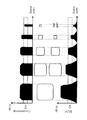
また、近年、微細パターンを形成するために、γ値が大きい高コントラストの化学増幅型レジスト膜が用いられている。例えば、図1の上側に示すように、ハーフトーン型位相シフトマスクブランクにおける位相シフト膜上のCr系遮光膜上にγ値が大きい高コントラストの化学増幅型レジストを用い電子線露光を行ってレジストパターンを形成する場合においては、高コントラストでシャープ(パターンエッジが垂直)なレジストパターンが得られ、例えば、1:1のラインアンドスペースパターンの設計寸法が500nm~70nmの範囲のレジストパターンのCDリニアリティも良好である。図1においてEthはレジストの解像が始まる最低露光量を表す。
このような反射型マスクは、基板上に露光光を反射する多層反射膜が形成され、該多層反射膜上にバッファ膜、さらにその上に露光光を吸収する吸収体膜がパターン状に形成されたものである。バッファ膜は、吸収体膜のパターン形成工程及び修正工程における多層反射膜の保護を目的として多層反射膜と吸収体膜との間に設けられている。露光機(パターン転写装置)に搭載された反射型マスクに入射した光は、吸収体膜のある部分では吸収され、吸収体膜のない部分では多層反射膜により反射された光像が反射光学系を通して半導体基板上に転写される。
上記の後方散乱により、反射型マスクブランクにおける吸収体膜上のγ値が大きい高コントラストの化学増幅型レジスト膜に対して電子線描画する際、パターンサイズの違いによって、レジスト膜中への蓄積エネルギーが大きく異なり、パターンサイズによって最低露光量Ethが異なることとなる(図1の下側の図参照)。したがって、高コントラストのレジストを用いてパターニングすると、CDリニアリティが低下してしまう(図1の下側の図の左から2番目のホールのサイズが、図1の上側の図の左から2番目のホールのサイズに比べ小さくなっていること参照)。また、図1の上側に示す、ハーフトーン型位相シフトマスクブランクにおけるCr系遮光膜上にγ値が大きい高コントラストの化学増幅型レジストのパターンを形成する場合に比べ、解像性能(最小解像線幅)が低下する(図1の下側の図の左から3~5番目のホールが解像していないこと参照)。
(構成1)
基板と、該基板上に形成された露光光を反射する多層反射膜と、該多層反射膜上に形成された露光光を吸収する吸収体膜と、を有する反射型マスクを作製するための反射型マスクブランクであって、
前記吸収体膜上に電子線描画用レジスト膜が設けられ、
前記電子線描画用レジスト膜のコントラスト値γが30以下であることを特徴とする反射型マスクブランク。
(構成2)
基板と、該基板上に形成された露光光を反射する多層反射膜と、該多層反射膜上に形成された露光光を吸収する吸収体膜と、を有する反射型マスクを作製するための反射型マスクブランクであって、
前記吸収体膜上に電子線描画用レジスト膜が設けられ、
前記電子線描画用レジスト膜の露光許容度が0.7nm/%Dose以下であることを特徴とする反射型マスクブランク。
(構成3)
前記レジスト膜のコントラスト値γが25以下であることを特徴とする構成1又は2記載の反射型マスクブランク。
(構成4)
前記反射型マスクブランクは、EUV光を露光光とするEUVリソグラフィで用いられる反射型マスクブランクであることを特徴とする構成1~3のいずれかに記載の反射型マスクブランク。
(構成5)
前記吸収体膜は、タンタルを含む材料からなることを特徴とする構成1~4のいずれかに記載の反射型マスクブランク。
(構成6)
前記多層反射膜の層数は、10周期以上であることを特徴とする構成1~5のいずれかに記載の反射型マスクブランク。
(構成7)
前記レジスト膜が化学増幅型レジストからなることを特徴とする構成1~6のいずれかに記載の反射型マスクブランク。
(構成8)
基板と、該基板上に形成された露光光を反射する多層反射膜と、該多層反射膜上に形成された露光光を吸収する吸収体膜と、を有する反射型マスクを作製するための反射型マスクブランクを準備する工程と、
前記吸収体膜上に、コントラスト値γが30以下である電子線描画用レジスト膜を設ける工程と、
電子線描画によってレジストパターンを形成する工程と、
を有することを特徴とする反射型マスクの製造方法。
(構成9)
基板と、該基板上に形成された露光光を反射する多層反射膜と、該多層反射膜上に形成された露光光を吸収する吸収体膜と、を有する反射型マスクを作製するための反射型マスクブランクを準備する工程と、
前記吸収体膜上に、露光許容度が0.7nm/%Dose以下である電子線描画用レジスト膜を設ける工程と、
電子線描画によってレジストパターンを形成する工程と、
を有することを特徴とする反射型マスクの製造方法。
(構成10)
前記レジスト膜のコントラスト値γが25以下であることを特徴とする構成8又は9に記載の反射型マスクの製造方法。
(構成11)
前記電子線描画において、電子線の加速電圧が50keV以上で露光することを特徴とする構成8~10のいずれかに8記載の反射型マスクの製造方法。
(構成12)
構成1から7のいずれかに記載のマスクブランクを用い、前記吸収体膜をパターニングして製造されたことを特徴とする反射型マスク。
基板と、該基板上に形成された露光光を反射する多層反射膜と、該多層反射膜上に形成された露光光を吸収する吸収体膜と、を有する反射型マスクを作製するための反射型マスクブランクであって、
前記吸収体膜上に電子線描画用レジスト膜が設けられ、
前記電子線描画用レジスト膜のコントラスト値γが30以下であることを特徴とする(構成1)。
このように、一般的なハーフトーン型位相シフトマスクブランクやバイナリマスクブランクに用いられる電子線描画用レジストよりも低コントラストの電子線描画用レジストを採用すると、露光感度に幅を持たせることできるため、後方散乱によって蓄積エネルギーが低下しても、CDリニアリティを良好にすることが可能となる。
詳しくは、図1の下側に示す図の場合、即ち反射型マスクブランクにおける吸収体膜上に、高コントラスト及び高解像性を意図して一般的に用いられるγ値が大きい高コントラストの化学増幅型レジストを用い電子線露光を行ってレジストパターンを形成する場合に比べ、本願発明の如く、図2の下側に示す図の場合、即ち反射型マスクブランクにおける吸収体膜上に、意図的にγ値が小さく低コントラストとなるように設計し作製した化学増幅型レジストを用い電子線露光を行ってレジストパターンを形成する場合は、CDリニアリティが良好となる(図1の下側の図の左から2番目のホールのサイズが、図1の上側の図の左から2番目のホールのサイズに比べ小さくなっているのに対し、図2の下側の図の左から2~4番目のホールのサイズが、図2の上側の図の左から2~4番目のホールのサイズ(設計寸法にほぼ対応する)に等しく、CDリニアリティが良好となること参照)。
また、図1の下側に示す図の場合、即ち反射型マスクブランクにおける吸収体膜上に、高コントラスト及び高解像性を意図して一般的に用いられるγ値が大きい高コントラストの化学増幅型レジストを用い電子線露光を行ってレジストパターンを形成する場合に比べ、本願発明では、解像性能(最小解像線幅)が向上する(図2の下側の図の左から3~4番目のホールが解像していること参照)。
感度曲線は、ポジ型レジストの場合、未露光部の現像後の膜厚を100%とした規格化膜厚としてグラフにしたものである。感度曲線は、ネガ型レジストの場合、パターン形成に最適な露光量よりも十分に大きい露光量で露光した部分の膜厚を100%とする。
感度曲線の傾きからγ値を算出できる。
ポジ型レジストの場合、γ値は、規格化膜厚が0(D0)から80%(D80)の間の傾きとする。
ポジ型レジストの場合、γ=0.8/log10(D0/D80)で表される。
γ値が大きいほど感度曲線の傾きが垂直に近づき、コントラストが高い。
γ値が低すぎると、レジストパターンのエッジのラフネスやCD分布に悪影響を与える。これを回避する観点から、γ値は10以上であることが好ましい。
ネガ型レジストの場合、γ=0.2/log10(D70/D50)で表される。
なお、γ値は感度に影響しない。
詳しくは、反射型マスクブランクにおける吸収体膜上に、高コントラスト及び高解像性を意図して一般的に用いられるγ値が大きい高コントラストの化学増幅型レジストを用い電子線露光を行ってレジストパターンを形成する場合においては、ハーフトーン型位相シフトマスクブランクやバイナリマスクブランクにおけるCr系遮光膜上のレジスト膜に対する場合と比較して、後方散乱が多く生じるため、レジスト膜中に蓄積するエネルギーが減少してしまい、特にパターンエッジ部分での蓄積エネルギーのコントラストが悪化し、これに基づきレジストパターンのCDリニアリティが低下してしまう。このような課題に対し、本願発明は、反射型マスクブランクにおける吸収体膜上に、このような課題を解決できるように、意図的にγ値が小さく低コントラストとなるように設計し作製した化学増幅型レジストを用い電子線露光を行ってレジストパターンを形成することを特徴とする。
化学増幅型レジストは、γ値が大きい高コントラスト(感度曲線が垂直に近く、露光感度の幅が非常に小さい)ことが特徴であるが、本発明では、あえてγ値が小さく低コントラスト(感度曲線の傾きをゆるくし、露光感度に幅を持たせる)となるように設計し作製した化学増幅型レジストを用い電子線露光を行ってレジストパターンを形成することによって、上記課題を解決することを特徴とする。
基板と、該基板上に形成された露光光を反射する多層反射膜と、該多層反射膜上に形成された露光光を吸収する吸収体膜と、を有する反射型マスクを作製するための反射型マスクブランクであって、
前記吸収体膜上に電子線描画用レジスト膜が設けられ、
前記電子線描画用レジスト膜の露光許容度が0.7nm/%Dose以下であることを特徴とする(構成2)。
ここで、露光許容度EL(Exposure Latitude)は、正規の設計CDが得られるドーズ量に対して、そのドーズ量を1%変動させたときに何nmCDが変化するかで表す。横軸にドーズ量をとり、縦軸にCDをとったドーズ量-CDのグラフにおいて、ポジ型レジストにホールパターンを形成する場合では、ドーズ量を高くするとCDが大きくなり、ドーズ量を小さくするとCDが小さくなる、右肩上がりの曲線が得られる。露光許容度ELは、この曲線の傾きで表わされる。
露光許容度ELは、0.7nm/%Dose以下であることが好ましい。また、露光許容度ELは、近接効果補正のため、0.5nm/%Dose以上であることが好ましい。
後述するように、電子線描画用レジストのコントラスト値γが小さくなるに従い、露光許容度ELの値も小さくなる傾向がみられる。したがって、露光許容度ELが上記範囲であると、構成1と同様に、後方散乱によって蓄積エネルギーが低下しても、CDリニアリティを良好にすることが可能となる。
本発明では、電子線描画用レジストは、コントラスト値γが30以下であり、かつ、露光許容度が0.7nm/%Dose以下である場合が含まれる。
なお、露光許容度ELは感度に影響しない。
上述したように、EUVリソグラフィで用いられる反射型マスクブランクにおいては、多層反射膜によって後方散乱されて再びレジスト膜に入射する光の影響が大きいため、本願課題が特に問題となる。
なお、本発明の反射型マスクブランクを用いて製造される反射型マスクは、EUV光(波長0.2~100nm程度)を露光光として用いるEUVリソグラフィに特に好適であるが、他の短波長の露光光に対しても適宜用いることは可能である。
上述したように、EUVリソグラフィで用いられる反射型マスクブランクにおいては、レジスト膜下層の吸収体膜がCrやMoよりも原子量の大きいタンタル(Ta)であることによって後方散乱されて再びレジスト膜に入射する光の影響も原因の一つであると考えられ、本願課題が問題となる。
吸収体膜の材料等に関しては後述する。
前記多層反射膜の層数が10周期(10ペア)以上であると、本願課題が特に問題となる。
前記多層反射膜の層数は、反射率の観点から、40~60周期(ペア)であることが好ましい。前記多層反射膜の膜厚は、例えば、280~420nmであることがより好ましい。
多層反射膜の材料等に関しては後述する。
上述したように、微細パターンを形成するために、γ値が大きい高コントラストの電子線描画用の化学増幅型レジスト膜が用いられている。また、この場合に本願課題が特に問題となる。
前記レジスト膜の膜厚は、50~200nmであることが好ましく、100~150nmであることがより好ましい。
なお、非化学増幅型レジストでは、50keV以上で露光(適正なドーズ量で描画)でき、高コントラストなレジストは得られ難い。これは、化学増幅型レジストでないと、高コントラストは得られ難いからである。なお、フォトレジストでは、電子線の後方散乱の課題が生じない。
基板と、該基板上に形成された露光光を反射する多層反射膜と、該多層反射膜上に形成された露光光を吸収する吸収体膜と、を有する反射型マスクを作製するための反射型マスクブランクを準備する工程と、
前記吸収体膜上に、コントラスト値γが30以下である電子線描画用レジスト膜を設ける工程と、
電子線描画によってレジストパターンを形成する工程と、
を有することを特徴とする(構成8)。
このような構成によると、上記と同様の効果が得られる。
基板と、該基板上に形成された露光光を反射する多層反射膜と、該多層反射膜上に形成された露光光を吸収する吸収体膜と、を有する反射型マスクを作製するための反射型マスクブランクを準備する工程と、
前記吸収体膜上に、露光許容度が0.7nm/%Dose以下である電子線描画用レジスト膜を設ける工程と、
電子線描画によってレジストパターンを形成する工程と、
を有することを特徴とする(構成9)。
このような構成によると、上記と同様の効果が得られる。
レジスト膜をより低コントラストにすることによって、CDリニアリティをさらに良好にすることが可能となる。
本発明において、前記電子線描画において、電子線の加速電圧が50keV以上で露光する場合が含まれる(構成11)。
加速電圧が大きいほど後方散乱が大きくなる。電子線の加速電圧が50keV以上であると、本願課題が特に問題となる。
上記構成1から7のいずれかに記載のマスクブランクを用い、前記吸収体膜をパターニングして製造されたことを特徴とする(構成12)。
本発明の反射型マスクとしては、以下のような態様が挙げられる。
(1)基板上に形成された多層反射膜上にバッファ膜が形成され、このバッファ膜上に所定の転写パターンを有する吸収体膜パターンが形成された反射型マスク(バッファ膜がパターニングされていないタイプの反射型マスク)。
(2)基板上に形成された多層反射膜上に、所定の転写パターンを有するバッファ膜と吸収体膜のパターンが形成された反射型マスク(バッファ膜がパターニングされているタイプの反射型マスク)。
(3)基板上に形成された多層反射膜上に、所定の転写パターンを有する吸収体膜パターンが形成された反射型マスク(バッファ膜がないタイプの反射型マスク)。
例えば、波長13~14nmのEUV光に対する多層反射膜としては、Mo膜とSi膜を交互に40周期程度積層したMo/Si周期積層膜が好ましく用いられる。その他に、EUV光の領域で使用される多層反射膜として、Ru/Si周期多層膜、Mo/Be周期多層膜、Mo化合物/Si化合物周期多層膜、Si/Nb周期多層膜、Si/Mo/Ru周期多層膜、Si/Mo/Ru/Mo周期多層膜、Si/Ru/Mo/Ru周期多層膜などがある。露光波長により、材質を適宜選択すればよい。
なお、本発明では、多層反射膜とバッファ膜との間、あるいは、多層反射膜と吸収体膜との間(バッファ膜を有していない場合)に、例えばルテニウム(Ru)又はその化合物等の材料からなる保護膜を設けてもよい。この保護膜を有することにより、バッファ膜や吸収体膜のパターン形成時のエッチングによる多層反射膜のダメージが防止され、露光光反射率の低下を防止できる。なお、上記ルテニウム化合物としては、例えば、RuNb、RuZr等が挙げられる。
本発明においては、クロム系バッファ膜の材料としては、特にクロム(Cr)の窒化物を含む材料が好ましく挙げられる。また、バッファ膜の膜密度が5.0~9.0g/cm3であることが好ましい。クロムの窒化物を含むバッファ膜の膜密度が5.0~9.0g/cm3であることにより、バッファ膜のEUV光に対する吸収効果を高められ、吸収体膜の薄膜化を図ることができ、Shadowing効果による転写対象物に転写したときのパターン線幅の太りを低減できるという効果を奏する。
なお、バッファ膜の膜厚は、たとえば集束イオンビーム(FIB)を用いた吸収体膜パターンの修正を行う場合には、20~60nm程度とするのが好ましいが、FIBを用いない場合には、5~15nm程度とすることができる。
上述したように、本発明において、前記吸収体膜は、タンタルを含む材料からなる場合が含まれる。
タンタルを含む材料としては、特にTaの単体またはTaを主成分とする材料を好ましく用いることができる。Taを主成分とする材料は、たとえばTaの合金である。このような吸収体膜の結晶状態は、平滑性、平坦性の点から、アモルファス状又は微結晶の構造を有しているものが好ましい。
Taを主成分とする材料としては、例えばTaとBを含む材料、TaとNを含む材料、TaとBを含み、更にOとNの少なくとも何れかを含む材料、等を好適に用いることができる。Taに例えばBを加えることにより、アモルファス状の材料が容易に得られ、平滑性を向上させることができる。また、TaにNやOを加えれば、酸化に対する耐性が向上するため、経時的な安定性を向上させることができるという効果が得られる。
このような本発明のより好ましい実施の形態に係る反射型マスクブランクによれば、以下の効果を有する反射型マスクブランクおよびそれを用いて製造される反射型マスクが得られる。
つまり、最上層におけるマスク使用時の露光光透過率を高めて表面反射を抑制するとともに、露光光であるEUV光に対するマスクコントラストを向上させることができ、微細パターンを高精度でパターン転写を行える。
なお、平滑性を示す単位Rmsは、二乗平均平方根粗さであり、原子間力顕微鏡で測定することができる。また平坦度は、TIR(Total Indicated Reading)で示される表面の反り(変形量)を表す値で、基板表面を基準として最小自乗法で定められる平面を焦平面とし、この焦平面より上にある基板表面の最も高い位置と、焦平面より下にある基板表面の最も低い位置との高低差の絶対値である。
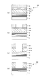
図8は本発明の反射型マスクブランクの一実施の形態及びこのマスクブランクを用いて反射型マスクを製造する工程を示す概略断面図である。
本発明の反射型マスクブランクの一実施の形態としては、図8(a)に示すように、基板1上に多層反射膜2が形成され、その上にバッファ膜3及び、下層4aと最上層4bの積層構造からなる吸収体膜4の各層が形成された構造をしている。また、吸収体膜4の上面にレジスト膜5を有している。
なお、図8に示す実施の形態では、反射型マスクブランク10は以上の如く構成され、バッファ膜を有しているが、吸収体膜4へのパターン形成の方法や形成したパターンの修正方法によっては、このバッファ膜を設けない構成としてもよい。
そして、この反射型マスクブランク10の吸収体膜4に所定の転写パターンを形成する。まず、吸収体膜4上のレジスト膜5に対して、電子線描画機を用いて所定のパターン描画を行い、これを現像して、所定のレジストパターン51を形成する(同図(b)参照)。
なお、最上層パターン41b上に残ったレジストパターン51は酸素プラズマアッシングやオゾン水等を用いて除去する。
ピンホール欠陥の修正には、例えば、FIBアシストデポジション法により炭素膜等をピンホールに堆積させるなどの方法がある。また、エッチング不足による欠陥の修正には、FIB照射による不要部分の除去を行うなどの方法がある。このとき、バッファ膜3は、FIB照射に対して、多層反射膜2を保護する保護膜となる。
最後に、仕様通りの寸法精度で吸収体膜パターンが形成されているかどうかの最終的な確認の検査を行う。
(反射型マスクブランクの作製)
使用する基板は、SiO2-TiO2系のガラス基板(6インチ角、厚さが6.3mm)である。この基板の熱膨張係数は0.2×10⁻⁷/℃、ヤング率は67GPaである。そして、このガラス基板は機械研磨により、0.2nmRms以下の平滑な表面と、100nm以下の平坦度に形成した。
基板上に形成される多層反射膜は、13~14nmの露光光波長帯域に適した多層反射膜とするために、Mo膜/Si膜周期多層反射膜を採用した。即ち、多層反射膜は、MoターゲットとSiターゲットを使用し、イオンビームスパッタリングにより基板上に交互に積層して形成した。Si膜を4.2nm、Mo膜を2.8nm、これを一周期として、40周期積層した後、Si膜を4.2nm成膜し、その上にさらに保護膜としてRu膜を2.5nmに成膜した。
このようにして多層反射膜付き基板を得た。この多層反射膜に対し、13.5nmのEUV光を入射角6.0度で反射率を測定したところ、反射率は63%であった。
続いて、吸収体膜の最上層として、TaとBとOを含む材料を20nmの厚さで形成した。即ち、Ta及びBを含むターゲットを用いて、アルゴン(Ar)に酸素(O2)を10%添加して、DCマグネトロンスパッタリング法によって成膜した。なお、成膜したTaBO膜の組成比は、Taが43at%、Bが8at%、Oが49at%であった。
なお、成膜したTaBN膜(下層)の膜密度は、13.5g/cm3であり、成膜したTaBO膜(最上層)の膜密度は、9.2g/cm3であった。膜密度の測定は、上記の方法によって行った。
また、上記最上層のTaBO膜に対し、13.5nmのEUV光を入射角6.0度で透過率を測定したところ、0.8%であった。
以上のようにして反射型マスクブランクを複数作製した。
化学増幅型レジストB:コントラスト値γ=33
化学増幅型レジストC:コントラスト値γ=27
化学増幅型レジストD:コントラスト値γ=12
化学増幅型レジストE:コントラスト値γ=11
ラインアンドスペース(L&S)のレジストパターンのCDリニアリティを図3に示す。
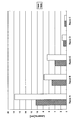
図3において、各レジストに関し左側の棒線(左肩上がりの斜線を施した棒線)は、限界解像の影響を受けにくい大きなパターン(500nm~100nmの範囲のL&Sパターン)で比較した場合であり、この条件によると、反射型マスクブランク上では、コントラスト値γが小さくなることにより、CDリニアリティが良くなる傾向があることがわかる。コントラスト値γが30以下であるレジストC,D,Eでは、デザインルールがDRAM hp32nmで要求される4.8nm以下のCDリニアリティを満たすことがわかる。
図3において、各レジストに関し右側の棒線は、500nm~70nmの範囲のL&Sパターンで比較した場合である。この条件によると、反射型マスクブランク上では、コントラスト値γが25以下であるレジストD、Eでは、デザインルールがDRAM hp23nmで要求される3.4nm以下のCDリニアリティを十分に満たすことがわかる。
化学増幅型レジストA、B、C、D、Eに関し、500nm~70nmの範囲のL&Sパターンのパターンサイズ(nm)と、CDリニアリティ(nm)との関係を、図4に示す。
図5に、化学増幅型レジストA、B、C、D、Eと、露光許容度EL(nm/%Dose)との関係を示す。このとき500nmの設計パターンで比較した。
図5に示すように、化学増幅型レジストA、B、C、D、Eのコントラスト値γが小さくなるに従い、露光許容度ELの値も小さくなる傾向がみられる。これによると、レジストC,D,Eでは、露光許容度ELが0.7nm/%Dose以下を満たしていることがわかる。
化学増幅型レジストBは、125nmのホールパターンを解像し、100nmのホールパターンは解像できない。化学増幅型レジストBは、60nmのL&Sパターンを解像し、50nmのL&Sパターンは解像できない。化学増幅型レジストBは、500~100nmの範囲のL&Sパターンに関し、レジストパターンのCDリニアリティは5.0nmであり、500nm~70nmの範囲のレジストパターンのCDリニアリティは7.7nmである。
化学増幅型レジストCは、100nmのホールパターンを解像し、80nmのホールパターンは解像できない。化学増幅型レジストCは、60nmのL&Sパターンを解像し、50nmのL&Sパターンは解像できない。化学増幅型レジストCは、500~100nmの範囲のL&Sパターンに関し、レジストパターンのCDリニアリティは3.9nmであり、500nm~70nmの範囲のレジストパターンのCDリニアリティは6.6nmである。
化学増幅型レジストDは、60nmのホールパターンを解像し、50nmのホールパターンは解像できない。化学増幅型レジストDは、50nmのL&Sパターンを解像し、45nmのL&Sパターンは解像できない。化学増幅型レジストDは、500~100nmの範囲のL&Sパターンに関し、レジストパターンのCDリニアリティは1.1nmであり、500nm~70nmの範囲のレジストパターンのCDリニアリティは1.5nmである。
化学増幅型レジストEは、80nmのホールパターンを解像し、70nmのホールパターンは解像できない。化学増幅型レジストEは、45nmのL&Sパターンを解像し、40nmのL&Sパターンは解像できない。化学増幅型レジストEは、500~100nmの範囲のL&Sパターンに関し、レジストパターンのCDリニアリティは0.7nmであり、500nm~70nmの範囲のレジストパターンのCDリニアリティは0.7nmである。
上記のように、コントラスト値γが小さくなることにより、解像性能(最小解像寸法)が向上し、CDリニアリティが向上することがわかる。
上記で得られた複数の反射型マスクブランク上に、上記に示す電子線描画用レジスト膜A~Eを各々形成し、電子線描画機を使用して所定のパターン描画を行い、描画後、現像によりレジストパターンを、上記と同様にして形成した。
さらに、塩素と酸素の混合ガスを用いて、反射領域上(吸収体膜のパターンのない部分)に残存しているバッファ膜を吸収体膜のパターンに従ってドライエッチングして除去し、表面にRu保護膜を備えた多層反射膜を露出させ、反射型マスクを得た。
膜厚が69nmのMoSi系位相シフト膜上に膜厚が48nmのCr系遮光膜を有する複数のハーフトーン型位相シフトマスクブランクの前記Cr系遮光膜上に、上記に示す電子線描画用レジスト膜A、Bを各々形成し、電子線描画機を使用して所定のパターン描画を行い、描画後、現像によりレジストパターンを形成した。電子線の加速電圧は50keVとした。
膜厚が60nmのMoSi系遮光膜を有するバイナリマスクブランクの前記MoSi系遮光膜上に、上記に示す電子線描画用レジスト膜Eを形成し、電子線描画機を使用して所定のパターン描画を行い、描画後、現像によりレジストパターンを形成した。電子線の加速電圧は50keVとした。
化学増幅型レジストA、B、Eに関し、500nm~70nmの範囲のL&Sパターンのパターンサイズ(nm)と、CDリニアリティ(nm)との関係を、図6に示す。いずれのレジストにおいても、500nm~70nmの範囲でCDリニアリティ(nm)は良好である。
図7において、各レジストに関し右側の棒線(右肩上がりの斜線を施した棒線)は、図6の結果、即ちハーフトーン型位相シフトマスク又はバイナリマスクブランク上に形成されたレジストパターンに関し、500nm~70nmの範囲のCDリニアリティ(nm)の範囲を示す。レジストA、B、EのCDリニアリティは、各々2.8nm、3.6nm、1.8nmで良好である。
図7において、各レジストに関し左側の棒線は、図3の右側の棒線、即ち反射型マスクブランク上に形成されたレジストパターンに関し、500nm~70nmの範囲のCDリニアリティ(nm)の範囲を示す。
図7から、ハーフトーン型位相シフトマスク又はバイナリマスクブランク上であれば、言い換えると反射型マスクブランク上でなければ、化学増幅型レジストA、B、Eはいずれも良好なCDリニアリティが得られることを示している。CDリニアリティの低下は反射型マスクブランク上に特有な現象である。
2 多層反射膜
3 バッファ膜
4 吸収体膜
4a 下層
4b 最上層
5 レジスト膜
10 反射型マスクブランク
20 反射型マスク
Claims (12)
- 基板と、該基板上に形成された露光光を反射する多層反射膜と、該多層反射膜上に形成された露光光を吸収する吸収体膜と、を有する反射型マスクを作製するための反射型マスクブランクであって、
前記吸収体膜上に電子線描画用レジスト膜が設けられ、
前記電子線描画用レジスト膜のコントラスト値γが30以下であることを特徴とする反射型マスクブランク。 - 基板と、該基板上に形成された露光光を反射する多層反射膜と、該多層反射膜上に形成された露光光を吸収する吸収体膜と、を有する反射型マスクを作製するための反射型マスクブランクであって、
前記吸収体膜上に電子線描画用レジスト膜が設けられ、
前記電子線描画用レジスト膜の露光許容度が0.7nm/%Dose以下であることを特徴とする反射型マスクブランク。 - 前記レジスト膜のコントラスト値γが25以下であることを特徴とする請求項1又は2記載の反射型マスクブランク。
- 前記反射型マスクブランクは、EUV光を露光光とするEUVリソグラフィで用いられる反射型マスクブランクであることを特徴とする請求項1~3のいずれかに記載の反射型マスクブランク。
- 前記吸収体膜は、タンタルを含む材料からなることを特徴とする請求項1~4のいずれかに記載の反射型マスクブランク。
- 前記多層反射膜の層数は、10周期以上であることを特徴とする請求項1~5のいずれかに記載の反射型マスクブランク。
- 前記レジスト膜が化学増幅型レジストからなることを特徴とする請求項1~6のいずれかに記載の反射型マスクブランク。
- 基板と、該基板上に形成された露光光を反射する多層反射膜と、該多層反射膜上に形成された露光光を吸収する吸収体膜と、を有する反射型マスクを作製するための反射型マスクブランクを準備する工程と、
前記吸収体膜上に、コントラスト値γが30以下である電子線描画用レジスト膜を設ける工程と、
電子線描画によってレジストパターンを形成する工程と、
を有することを特徴とする反射型マスクの製造方法。 - 基板と、該基板上に形成された露光光を反射する多層反射膜と、該多層反射膜上に形成された露光光を吸収する吸収体膜と、を有する反射型マスクを作製するための反射型マスクブランクを準備する工程と、
前記吸収体膜上に、露光許容度が0.7nm/%Dose以下である電子線描画用レジスト膜を設ける工程と、
電子線描画によってレジストパターンを形成する工程と、
を有することを特徴とする反射型マスクの製造方法。 - 前記レジスト膜のコントラスト値γが25以下であることを特徴とする請求項8又は9に記載の反射型マスクの製造方法。
- 前記電子線描画において、電子線の加速電圧が50keV以上で露光することを特徴とする請求項8~10のいずれかに記載の反射型マスクの製造方法。
- 請求項1から7のいずれかに記載のマスクブランクを用い、前記吸収体膜をパターニングして製造されたことを特徴とする反射型マスク。
Priority Applications (4)
| Application Number | Priority Date | Filing Date | Title |
|---|---|---|---|
| KR1020187006494A KR102127904B1 (ko) | 2010-07-30 | 2011-07-29 | 반사형 마스크 블랭크 및 그 제조 방법, 그리고 반사형 마스크 |
| US13/812,627 US8785086B2 (en) | 2010-07-30 | 2011-07-29 | Reflective mask blank, method of manufacturing the same, and reflective mask |
| KR1020197011946A KR102144730B1 (ko) | 2010-07-30 | 2011-07-29 | 반사형 마스크 블랭크 및 그 제조 방법, 그리고 반사형 마스크 |
| KR1020137001682A KR20130111523A (ko) | 2010-07-30 | 2011-07-29 | 반사형 마스크 블랭크 및 그 제조 방법, 그리고 반사형 마스크 |
Applications Claiming Priority (2)
| Application Number | Priority Date | Filing Date | Title |
|---|---|---|---|
| JP2010-172034 | 2010-07-30 | ||
| JP2010172034A JP5543873B2 (ja) | 2010-07-30 | 2010-07-30 | 反射型マスクブランク及びその製造方法、並びに反射型マスク |
Publications (1)
| Publication Number | Publication Date |
|---|---|
| WO2012014495A1 true WO2012014495A1 (ja) | 2012-02-02 |
Family
ID=45529721
Family Applications (1)
| Application Number | Title | Priority Date | Filing Date |
|---|---|---|---|
| PCT/JP2011/004321 Ceased WO2012014495A1 (ja) | 2010-07-30 | 2011-07-29 | 反射型マスクブランク及びその製造方法、並びに反射型マスク |
Country Status (5)
| Country | Link |
|---|---|
| US (1) | US8785086B2 (ja) |
| JP (1) | JP5543873B2 (ja) |
| KR (3) | KR20130111523A (ja) |
| TW (1) | TWI518445B (ja) |
| WO (1) | WO2012014495A1 (ja) |
Families Citing this family (7)
| Publication number | Priority date | Publication date | Assignee | Title |
|---|---|---|---|---|
| JP6301127B2 (ja) | 2013-12-25 | 2018-03-28 | Hoya株式会社 | 反射型マスクブランク及び反射型マスク、並びに半導体装置の製造方法 |
| WO2018153872A1 (en) * | 2017-02-25 | 2018-08-30 | Asml Netherlands B.V. | Patterning device, a method of making the same, and a patterning device design method |
| KR102617017B1 (ko) | 2017-08-10 | 2023-12-26 | 에이지씨 가부시키가이샤 | 반사형 마스크 블랭크 및 반사형 마스크 |
| JP6556885B2 (ja) * | 2018-02-22 | 2019-08-07 | Hoya株式会社 | 反射型マスクブランク及び反射型マスク、並びに半導体装置の製造方法 |
| US11402742B1 (en) * | 2018-02-28 | 2022-08-02 | Synopsys, Inc. | Undercut EUV absorber reflective contrast enhancement |
| JP7344628B2 (ja) * | 2021-04-30 | 2023-09-14 | エスケー エンパルス カンパニー リミテッド | フォトマスクブランク、フォトマスク及び半導体素子の製造方法 |
| JP7722257B2 (ja) | 2022-05-10 | 2025-08-13 | 信越化学工業株式会社 | マスクブランク、レジストパターン形成方法及び化学増幅ポジ型レジスト組成物 |
Citations (5)
| Publication number | Priority date | Publication date | Assignee | Title |
|---|---|---|---|---|
| JPH06177018A (ja) * | 1992-12-07 | 1994-06-24 | Hitachi Ltd | 光学素子および光学素子の照明方法並びに投影露光装置 |
| JPH07333829A (ja) * | 1994-06-07 | 1995-12-22 | Hitachi Ltd | 光学素子およびその製造方法 |
| JPH0922862A (ja) * | 1995-07-07 | 1997-01-21 | Nikon Corp | X線反射型マスクの製造方法 |
| JP2001133967A (ja) * | 1999-11-10 | 2001-05-18 | Hitachi Ltd | 感放射線組成物、パタン形成方法およびこれを用いた位相シフトマスクの製造方法 |
| JP2009147200A (ja) * | 2007-12-17 | 2009-07-02 | Toppan Printing Co Ltd | 反射型フォトマスク、反射型フォトマスク製造方法 |
Family Cites Families (4)
| Publication number | Priority date | Publication date | Assignee | Title |
|---|---|---|---|---|
| JPH08213303A (ja) | 1995-02-03 | 1996-08-20 | Nikon Corp | 反射型x線マスク及びその製造法 |
| US7022247B2 (en) * | 2003-03-26 | 2006-04-04 | Union Semiconductor Technology Corporation | Process to form fine features using photolithography and plasma etching |
| JP2007266030A (ja) * | 2006-03-27 | 2007-10-11 | Seiko Epson Corp | 半導体装置の製造方法および半導体装置 |
| JP2008078551A (ja) * | 2006-09-25 | 2008-04-03 | Toppan Printing Co Ltd | 反射型フォトマスクブランク及び反射型フォトマスク並びに半導体装置の製造方法 |
-
2010
- 2010-07-30 JP JP2010172034A patent/JP5543873B2/ja active Active
-
2011
- 2011-07-29 TW TW100126948A patent/TWI518445B/zh active
- 2011-07-29 KR KR1020137001682A patent/KR20130111523A/ko not_active Ceased
- 2011-07-29 KR KR1020197011946A patent/KR102144730B1/ko active Active
- 2011-07-29 WO PCT/JP2011/004321 patent/WO2012014495A1/ja not_active Ceased
- 2011-07-29 US US13/812,627 patent/US8785086B2/en active Active
- 2011-07-29 KR KR1020187006494A patent/KR102127904B1/ko active Active
Patent Citations (5)
| Publication number | Priority date | Publication date | Assignee | Title |
|---|---|---|---|---|
| JPH06177018A (ja) * | 1992-12-07 | 1994-06-24 | Hitachi Ltd | 光学素子および光学素子の照明方法並びに投影露光装置 |
| JPH07333829A (ja) * | 1994-06-07 | 1995-12-22 | Hitachi Ltd | 光学素子およびその製造方法 |
| JPH0922862A (ja) * | 1995-07-07 | 1997-01-21 | Nikon Corp | X線反射型マスクの製造方法 |
| JP2001133967A (ja) * | 1999-11-10 | 2001-05-18 | Hitachi Ltd | 感放射線組成物、パタン形成方法およびこれを用いた位相シフトマスクの製造方法 |
| JP2009147200A (ja) * | 2007-12-17 | 2009-07-02 | Toppan Printing Co Ltd | 反射型フォトマスク、反射型フォトマスク製造方法 |
Also Published As
| Publication number | Publication date |
|---|---|
| KR20180029096A (ko) | 2018-03-19 |
| US20130122407A1 (en) | 2013-05-16 |
| US8785086B2 (en) | 2014-07-22 |
| KR102127904B1 (ko) | 2020-07-09 |
| JP5543873B2 (ja) | 2014-07-09 |
| KR20130111523A (ko) | 2013-10-10 |
| TW201217901A (en) | 2012-05-01 |
| KR102144730B1 (ko) | 2020-08-14 |
| TWI518445B (zh) | 2016-01-21 |
| KR20190047118A (ko) | 2019-05-07 |
| JP2012033715A (ja) | 2012-02-16 |
Similar Documents
| Publication | Publication Date | Title |
|---|---|---|
| JP5507876B2 (ja) | 反射型マスクブランク及び反射型マスクの製造方法 | |
| JP5638769B2 (ja) | 反射型マスクブランクの製造方法及び反射型マスクの製造方法 | |
| JP5974321B2 (ja) | 反射型マスクブランク及び反射型マスクの製造方法 | |
| KR20250153880A (ko) | 반사형 마스크 블랭크, 반사형 마스크, 및 반도체 장치의 제조 방법 | |
| JP5543873B2 (ja) | 反射型マスクブランク及びその製造方法、並びに反射型マスク | |
| JP6425951B2 (ja) | 反射型マスクブランク及びその製造方法、反射型マスクの製造方法、並びに半導体装置の製造方法 | |
| JP4792147B2 (ja) | 反射型マスクブランクス及び反射型マスク | |
| JP4926521B2 (ja) | 反射型マスクブランクス及び反射型マスク並びに半導体装置の製造方法 | |
| KR20250159076A (ko) | 반사형 마스크 블랭크, 반사형 마스크, 반사형 마스크의 제조 방법, 및 반도체 장치의 제조 방법 | |
| JP2022117747A (ja) | 描画評価用マスクブランクス | |
| JP2012159855A (ja) | マスクブランクの製造方法及びマスクの製造方法 |
Legal Events
| Date | Code | Title | Description |
|---|---|---|---|
| 121 | Ep: the epo has been informed by wipo that ep was designated in this application |
Ref document number: 11812092 Country of ref document: EP Kind code of ref document: A1 |
|
| ENP | Entry into the national phase |
Ref document number: 20137001682 Country of ref document: KR Kind code of ref document: A |
|
| WWE | Wipo information: entry into national phase |
Ref document number: 13812627 Country of ref document: US |
|
| NENP | Non-entry into the national phase |
Ref country code: DE |
|
| 122 | Ep: pct application non-entry in european phase |
Ref document number: 11812092 Country of ref document: EP Kind code of ref document: A1 |