WO2012008686A2 - Printing plate and method of manufacturing the same - Google Patents
Printing plate and method of manufacturing the same Download PDFInfo
- Publication number
- WO2012008686A2 WO2012008686A2 PCT/KR2011/004101 KR2011004101W WO2012008686A2 WO 2012008686 A2 WO2012008686 A2 WO 2012008686A2 KR 2011004101 W KR2011004101 W KR 2011004101W WO 2012008686 A2 WO2012008686 A2 WO 2012008686A2
- Authority
- WO
- WIPO (PCT)
- Prior art keywords
- pattern
- printing plate
- printing
- resin layer
- photosensitive resin
- Prior art date
- Legal status (The legal status is an assumption and is not a legal conclusion. Google has not performed a legal analysis and makes no representation as to the accuracy of the status listed.)
- Ceased
Links
Images




Classifications
-
- G—PHYSICS
- G03—PHOTOGRAPHY; CINEMATOGRAPHY; ANALOGOUS TECHNIQUES USING WAVES OTHER THAN OPTICAL WAVES; ELECTROGRAPHY; HOLOGRAPHY
- G03F—PHOTOMECHANICAL PRODUCTION OF TEXTURED OR PATTERNED SURFACES, e.g. FOR PRINTING, FOR PROCESSING OF SEMICONDUCTOR DEVICES; MATERIALS THEREFOR; ORIGINALS THEREFOR; APPARATUS SPECIALLY ADAPTED THEREFOR
- G03F7/00—Photomechanical, e.g. photolithographic, production of textured or patterned surfaces, e.g. printing surfaces; Materials therefor, e.g. comprising photoresists; Apparatus specially adapted therefor
- G03F7/004—Photosensitive materials
- G03F7/09—Photosensitive materials characterised by structural details, e.g. supports, auxiliary layers
- G03F7/095—Photosensitive materials characterised by structural details, e.g. supports, auxiliary layers having more than one photosensitive layer
-
- G—PHYSICS
- G02—OPTICS
- G02F—OPTICAL DEVICES OR ARRANGEMENTS FOR THE CONTROL OF LIGHT BY MODIFICATION OF THE OPTICAL PROPERTIES OF THE MEDIA OF THE ELEMENTS INVOLVED THEREIN; NON-LINEAR OPTICS; FREQUENCY-CHANGING OF LIGHT; OPTICAL LOGIC ELEMENTS; OPTICAL ANALOGUE/DIGITAL CONVERTERS
- G02F1/00—Devices or arrangements for the control of the intensity, colour, phase, polarisation or direction of light arriving from an independent light source, e.g. switching, gating or modulating; Non-linear optics
- G02F1/01—Devices or arrangements for the control of the intensity, colour, phase, polarisation or direction of light arriving from an independent light source, e.g. switching, gating or modulating; Non-linear optics for the control of the intensity, phase, polarisation or colour
- G02F1/13—Devices or arrangements for the control of the intensity, colour, phase, polarisation or direction of light arriving from an independent light source, e.g. switching, gating or modulating; Non-linear optics for the control of the intensity, phase, polarisation or colour based on liquid crystals, e.g. single liquid crystal display cells
-
- G—PHYSICS
- G02—OPTICS
- G02F—OPTICAL DEVICES OR ARRANGEMENTS FOR THE CONTROL OF LIGHT BY MODIFICATION OF THE OPTICAL PROPERTIES OF THE MEDIA OF THE ELEMENTS INVOLVED THEREIN; NON-LINEAR OPTICS; FREQUENCY-CHANGING OF LIGHT; OPTICAL LOGIC ELEMENTS; OPTICAL ANALOGUE/DIGITAL CONVERTERS
- G02F1/00—Devices or arrangements for the control of the intensity, colour, phase, polarisation or direction of light arriving from an independent light source, e.g. switching, gating or modulating; Non-linear optics
- G02F1/01—Devices or arrangements for the control of the intensity, colour, phase, polarisation or direction of light arriving from an independent light source, e.g. switching, gating or modulating; Non-linear optics for the control of the intensity, phase, polarisation or colour
- G02F1/13—Devices or arrangements for the control of the intensity, colour, phase, polarisation or direction of light arriving from an independent light source, e.g. switching, gating or modulating; Non-linear optics for the control of the intensity, phase, polarisation or colour based on liquid crystals, e.g. single liquid crystal display cells
- G02F1/133—Constructional arrangements; Operation of liquid crystal cells; Circuit arrangements
- G02F1/136—Liquid crystal cells structurally associated with a semi-conducting layer or substrate, e.g. cells forming part of an integrated circuit
- G02F1/1362—Active matrix addressed cells
- G02F1/136286—Wiring, e.g. gate line, drain line
-
- G—PHYSICS
- G03—PHOTOGRAPHY; CINEMATOGRAPHY; ANALOGOUS TECHNIQUES USING WAVES OTHER THAN OPTICAL WAVES; ELECTROGRAPHY; HOLOGRAPHY
- G03F—PHOTOMECHANICAL PRODUCTION OF TEXTURED OR PATTERNED SURFACES, e.g. FOR PRINTING, FOR PROCESSING OF SEMICONDUCTOR DEVICES; MATERIALS THEREFOR; ORIGINALS THEREFOR; APPARATUS SPECIALLY ADAPTED THEREFOR
- G03F7/00—Photomechanical, e.g. photolithographic, production of textured or patterned surfaces, e.g. printing surfaces; Materials therefor, e.g. comprising photoresists; Apparatus specially adapted therefor
- G03F7/0035—Multiple processes, e.g. applying a further resist layer on an already in a previously step, processed pattern or textured surface
-
- G—PHYSICS
- G03—PHOTOGRAPHY; CINEMATOGRAPHY; ANALOGOUS TECHNIQUES USING WAVES OTHER THAN OPTICAL WAVES; ELECTROGRAPHY; HOLOGRAPHY
- G03F—PHOTOMECHANICAL PRODUCTION OF TEXTURED OR PATTERNED SURFACES, e.g. FOR PRINTING, FOR PROCESSING OF SEMICONDUCTOR DEVICES; MATERIALS THEREFOR; ORIGINALS THEREFOR; APPARATUS SPECIALLY ADAPTED THEREFOR
- G03F7/00—Photomechanical, e.g. photolithographic, production of textured or patterned surfaces, e.g. printing surfaces; Materials therefor, e.g. comprising photoresists; Apparatus specially adapted therefor
- G03F7/20—Exposure; Apparatus therefor
- G03F7/2022—Multi-step exposure, e.g. hybrid; backside exposure; blanket exposure, e.g. for image reversal; edge exposure, e.g. for edge bead removal; corrective exposure
-
- G—PHYSICS
- G03—PHOTOGRAPHY; CINEMATOGRAPHY; ANALOGOUS TECHNIQUES USING WAVES OTHER THAN OPTICAL WAVES; ELECTROGRAPHY; HOLOGRAPHY
- G03F—PHOTOMECHANICAL PRODUCTION OF TEXTURED OR PATTERNED SURFACES, e.g. FOR PRINTING, FOR PROCESSING OF SEMICONDUCTOR DEVICES; MATERIALS THEREFOR; ORIGINALS THEREFOR; APPARATUS SPECIALLY ADAPTED THEREFOR
- G03F7/00—Photomechanical, e.g. photolithographic, production of textured or patterned surfaces, e.g. printing surfaces; Materials therefor, e.g. comprising photoresists; Apparatus specially adapted therefor
- G03F7/26—Processing photosensitive materials; Apparatus therefor
- G03F7/40—Treatment after imagewise removal, e.g. baking
Definitions
- the embodiments of the present invention are directed to a printing plate for manufacturing an electronic substrate and a display apparatus and a method of manufacturing the printing plate.
- Circuits for electronic parts or various patterns may be printed using a direct printing method, such as, for example, inkjet printing, or an indirect printing method, such as, for example, gravure printing or offset printing.
- a direct printing method such as, for example, inkjet printing
- an indirect printing method such as, for example, gravure printing or offset printing.
- the gravure or offset printing uses a printing plate commonly called “cliche”.
- a printing plate with a pattern may be manufactured by etching a substrate or by performing photolithography on a plate coated with a photosensitive resin.
- a PR pattern forming process is a critical process that has a great effect on capability of devices for driving the display apparatus, such as thin film transistors (TFTs).
- TFTs thin film transistors
- Various researches are in progress to enhance capability of the devices, for example, by forming micro metal patterns.
- a PR pattern forming process a photoresist (PR) material is applied as a photosensitive material on a substrate, exposed to light using a mask, and then developed.
- PR pattern forming process is, however, too complicate and disadvantage in terms of costs especially when a plurality of patterns are formed for producing the devices because a separate photoresist process needs to be performed for each of the patterns.
- PR pattern formation using printing has been suggested.
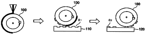
- Fig. 1 illustrates a method of manufacturing a printing plate according to a related art.
- a photoresist pattern a2 is not directly transferred from a first transparent insulation substrate 110 that has a printing pattern a1 and is used as a printing plate to a second transparent insulation substrate 120 that is subjected to printing. Rather, the photoresist pattern a2 is first transferred to a blanket 100 that has a surface formed of silicon rubber and serves as a medium, and the pattern a2 transferred to the blanket 100 is then transferred to the second transparent insulation substrate 120.
- a printing pattern etched on a printing plate has better printing characteristics.
- the width increases correspondingly.
- Exemplary embodiments of the present invention provide a printing plate and a method of manufacturing the printing plate.
- micro printing patterns may be effectively formed, and the number of processes may be reduced to save manufacturing costs.
- micro printing patterns using a printing plate may be performed by an indirect printing method, wherein the printing plate may be used to print various electronic circuits and patterns.
- the printing plate may be used to print various electronic circuits and patterns.
- a printing plate may be formed by performing imprinting on a photosensitive resin and a thermosetting resin using a metal or glass mold. Accordingly, micro patterns having different widths or different depths may be formed with simplified processes, thus lowering manufacturing costs.
- a functional layer may be formed of a photosensitive resin on printing patterns.
- the functional layer may protect the printing patterns from contaminants and may enhance matching characteristics between a printing ink and the printing patterns to increase printing quality. Further, the functional layer may allow for a printing plate for large-sized micro pattern printing.
- a printing plate comprising a substrate having a first surface and a second surface opposite to the first surface, and a resin layer having a plurality of printing patterns on the first surface of the substrate.
- Printing patterns having various structures and high accuracy may be formed by illumination patterning using a photosensitive resin as the resin layer or by laser writing.
- printing patterns having uniform shapes or having different depths and widths may be formed.
- an adhesive layer may be formed to enhance adhesion between the resin layer and the substrate, and a functional layer may be formed on the printing patterns for protection. This provides reliability.
- micro printing patterns may be effectively formed, and the number of processes may be reduced to save manufacturing costs. Further, it is possible to easily adjust a ratio of a depth with respect to a width of the patterns, thus enhancing uniformity and preventing the printing plate from collapsing at the printing pattern regions. Accordingly, a printing plate with enhanced durability may be provided.
- micro printing patterns using a printing plate may be performed by an indirect printing method, wherein the printing plate may be used to print various electronic circuits and patterns.
- the printing plate may be used to print various electronic circuits and patterns.
- a printing plate may be formed by performing imprinting on a photosensitive resin and a thermosetting resin using a metal or glass mold. Accordingly, micro patterns having different widths or different depths may be formed with simplified processes, thus lowering manufacturing costs.
- the embodiments of the present invention employ an imprinting process, and thus, a printing plate that includes printing patterns having different depths along the pattern width may be formed by a single process. Due to a base resin layer formed during imprinting, adhesion to the substrate may be increased.
- a functional layer may be formed of a photosensitive resin on printing patterns.
- the functional layer may protect the printing patterns from contaminants and may enhance matching characteristics between a printing ink and the printing patterns to increase printing quality. Further, the functional layer may allow for a printing plate for large-sized micro pattern printing.
- Fig. 1 illustrates a method of manufacturing a printing plate according to a related art
- Figs. 2 and 3 illustrate structures of printing plates according to embodiments of the present invention
- Figs. 4 and 5 illustrate a process of manufacturing a printing plate according to an embodiment of the present invention
- Fig. 6 illustrates images of a printing plate actually implemented according to an embodiment of the present invention
- Fig. 7 illustrates a structure of a printing plate according to an embodiment of the present invention
- Figs. 8 and 9 illustrate processes of manufacturing a printing plate according to an embodiment of the present invention
- Fig. 10 illustrates a structure of a printing plate according to an embodiment of the present invention
- Figs. 11 and 12 illustrate processes of manufacturing a printing plate according to an embodiment of the present invention
- Fig. 13 illustrates a process of manufacturing a printing plate according to an embodiment of the present invention
- Fig. 14 illustrates a structure of a printing plate according to an embodiment of the present invention.
- Figs. 15 and 16 illustrate a process of manufacturing a printing plate according to an embodiment of the present invention.
- a printing plate includes a first surface and a second surface opposite to the first surface.
- the first surface of the printing plate includes a resin layer a surface of which has a plurality of printing patterns.
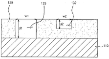
- Figs. 2 and 3 illustrate structures of printing plates according to embodiments of the present invention.
- a printing plate includes first and second printing patterns 123 and 132 formed by patterning a photosensitive resin layer 120 deposited on a substrate 110.
- the first and second printing patterns 123 and 132 have different depths and different widths from each other.
- the first printing pattern 123 is a reference pattern
- the second pattern 132 is a minimum pattern. According to an embodiment, more printing patterns that those illustrated in Fig. 2 may be formed that have different depths and widths from one another.
- a ratio of a line width and a depth of a printing pattern may be in a range of 1 : (0.5 ⁇ 4).
- a depth of the first pattern 123 is the same as a thickness of the photosensitive resin layer 120
- the embodiments of the present invention are not limited thereto, and according to an embodiment, the depth of the first pattern 123 may be less than the thickness of the photosensitive resin layer 120.
- a depth of the second pattern 132 may be less than the thickness of the photosensitive resin layer 120.
- the depth d1 and the width w1 of the first pattern 123 may be more than the depth d2 and the width w2 of the second pattern 132.
- a functional layer 140 may be formed of a metal material selected from Cr, Mo, Ta, and Ni, an organic material selected from Parylene and Teflon, or an inorganic material selected from SiOx, SiNx, and diamond-like carbon (DLC), on the substrate 110 and the printing patterns 123 and 132.
- a metal material selected from Cr, Mo, Ta, and Ni
- an organic material selected from Parylene and Teflon
- the structure shown in Fig. 3 is identical in material and printing patterns to the structure shown in Fig. 2 except for the structure of the first pattern 123. This characteristic difference in structure may originate from a manufacturing process shown in Fig. 5.
- the first pattern 123 is formed so that a width W1 of the upper portion is larger than a width W1’ of the lower portion to maximize alignment efficiency.
- a difference between the width W1 and the widths W1’ may be in a range of 5 to 20um.
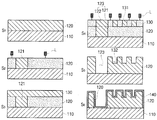
- Figs. 4 and 5 illustrate a process of manufacturing a printing plate according to an embodiment of the present invention.
- the manufacturing process may be implemented in various manners depending on methods of forming a photosensitive resin layer on a substrate and forming a printing pattern on the resin layer.
- the manufacturing process includes applying a first photosensitive resin on a substrate and exposing to light to thereby form a lower portion of a first pattern, applying a second photosensitive resin on the first photosensitive resin and exposing to light to form an upper portion of the first pattern and a second pattern, and simultaneously developing the first and second photosensitive resins to form the first and second patterns.
- the printing patterns may be complete by performing application of the photosensitive resin and exposure to light at the same time and by performing batch development after the formation of the second pattern.
- the embodiments of the present invention are not limited thereto. According to an embodiment, exposing and developing steps may be separately conducted for each photosensitive resin layer to form the printing patterns.
- step S1 a photosensitive resin is applied on a substrate 110 to form a first photosensitive resin layer 120.
- any types of materials may be used as the substrate 110 as long as the materials allow for surface flatness, large size, and a similar thermal expansion coefficient even after transfer.
- glass, polymer, such as PC, PMMA, or PET, or metal may be used for the substrate 110.
- the photosensitive resin may be formed using general spin coating or slit coating.
- Various materials such as photoresists, dry film resists, or UV cured resins, may be used as the photosensitive resin.
- any materials having photosensitive characteristics such as, for example, epoxy-based, polyimide-based, Novolak-based resins, may also be employed as the photosensitive resin.
- step S2 the first photosensitive resin layer 120 is exposed to light to form the lower portion 121 of the first pattern.
- a laser writer L may be used for patterning.
- the lower portion of the first pattern may be complete by performing development immediately after patterning by exposure to light. In the present embodiment, however, the exposing step may also be performed.
- a negative photosensitive material is used that forms a pattern at a portion that is not illuminated with a laser beam.
- a positive photosensitive material may also be used that forms a pattern in a manner opposite to that of the negative photosensitive material.
- step S3 a photosensitive material is applied on the patterned first photosensitive resin layer to form a second photosensitive resin layer 130.
- step S4 second exposure to light is performed on the second photosensitive resin layer 130 to pattern a second pattern 131 and an upper portion 122 of the first pattern.
- step S5 if portions not exposed to light are simultaneously removed (developed), a printing plate is complete that has the first and second patterns 123 and 132.
- the first pattern 123 has larger width and depth than those of the second pattern 132.
- a ratio of the width to the depth of each of the first and second patterns may be in a range 1 : (0.5 ⁇ 1.4).
- a function layer 140 may be formed on the first and second patterns.
- the function layer 140 may be formed of a a metal material selected from Cr, Mo, Ta, and Ni, an organic material selected from Parylene and Teflon, or an inorganic material selected from SiOx, SiNx, and diamond-like carbon (DLC), using one selected from spin coating, spray coating, sputtering, and chemical vapor deposition (CVD).
- the functional layer 140 may enhance durability and printing characteristics of the printing patterns.
- the function layer 140 may be formed of a material, such as a-Si, SiNx, or SiOx.
- the manufacturing process as described above forms patterns by performing photolithography on the photosensitive resin, and accordingly, has merits that micro patterns may be easily formed and the number of processes may be reduced compared to the conventional wet/dry etching methods, thus capable of manufacturing low-cost printing plates. Further, in comparison with an existing method of adjusting the depth of a pattern by randomly not developing a photosensitive resin, the manufacturing process according to the embodiments of the present invention may easily adjust a ratio of a depth and a width of a pattern, may increase uniformity of the depth, and may prevent the printing plate from collapsing at micro pattern regions, thus enhancing durability.
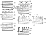
- Fig. 5 illustrates a process of manufacturing a printing plate according to an embodiment of the present invention.
- an exposing process is performed using a photomask unlike the embodiment described in connection with Fig. 4 that performs patterning through exposure of the photosensitive resin layer to light.
- a first photosensitive material layer 120 is formed on a substrate 110.
- a lower portion 121 of a first pattern is formed by an exposure system (e.g., UV exposure system) through the medium of a photomask.
- a second photosensitive material layer 130 is formed on the lower portion 121 and the layer 120.
- an upper portion 122 of the first pattern and a second pattern 131 are patterned using a photomask M.
- an alignment between patterns is critical.
- the lower portion 121 of the first pattern may be designed to be smaller than the upper portion 122 of the first pattern to enhance a process margin.
- step P5 the first and second photosensitive material layers are exposed to light at the same time to complete first and second patterns 123 and 132.
- predetermined step portions Q are formed in the first pattern 123.
- the lower portion is formed to be narrower than the upper portion.
- the difference in width may range from 5 to 20um.
- a functional layer 140 is formed, thus completing a printing plate.
- the first pattern 123 is formed to have larger width and depth than those of the second pattern 132.
- a ratio of a width and a depth of each pattern may be in a range of 1 : (0.5 ⁇ 1.4).
- processes, materials, and photosensitive materials for forming the functional layer may be the same as those of the embodiment described in connection with Fig. 3, and thus, repetitive description thereof will be omitted.
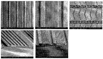
- Fig. 6 illustrates images of a printing plate actually implemented according to an embodiment of the present invention.
- the method of manufacturing a printing plate according to the embodiments of the present invention may configure micro patterns more efficiently than the conventional method of manufacturing a printing plate using wet etching, and may implement a high A/R (Aspect Ratio).
- the method according to the embodiments of the present invention may solve problems of a minimum width loss that occurs upon performing the conventional wet etching so that micro patterns may be easily implemented, and may considerably increase a ratio of a width and a depth of each micro pattern to enhance transfer characteristics.
- the method of manufacturing a printing plate according to the embodiments of the present invention may simplify the steps of implementing a printing plate compared to a method of manufacturing a printing plate by performing dry etching on a material film for dry etching, and may save manufacturing costs. Further, the method according to the embodiments of the present invention forms printing patterns using lithography, and thus, high patterning accuracy may be achieved.
- printing patterns are formed by patterning a photosensitive resin, micro patterns may be efficiently formed, and the number of processes may be reduced, thus saving manufacturing costs. Further, a ratio of a depth with respect to a width of each pattern may be easily adjusted, and depth uniformity may be raised. Accordingly, it may be possible to prevent the printing plate from collapsing at micro pattern regions, thus allowing for a durable printing plate.
- Fig. 7 illustrates a structure of a printing plate according to an embodiment of the present invention.
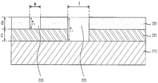
- a printing plate includes photosensitive resin layers 221 and 231 formed on a substrate 210, and a plurality of printing patterns 223 and 233 formed by patterning the photosensitive resin layers and having different widths and depths from each other.
- the substrate 110 Any types of materials may be used as the substrate 110 as long as the materials allow for surface flatness, large size, and a similar thermal expansion coefficient even after transfer.
- glass, polymer, such as PC, PMMA, or PET, or metal may be used for the substrate 110.
- the substrate may have a thermal expansion coefficient that is within two times of a thermal expansion coefficient of a transfer substrate.
- the embodiments of the present invention are not limited thereto. According to embodiments, more than two photosensitive resin layers may be formed that include printing patterns at least two of which have different depths from each other.
- the photosensitive resin layer formed on the substrate is referred to as “first photosensitive resin layer 221” and the other photosensitive resin layer formed on the first photosensitive resin layer 221 is referred to as “second photosensitive resin layer 231”.
- the first and second photosensitive resin layers may be formed using general spin coating or slit coating.
- Various materials, such as photoresists, dry film resists, or UV cured resins may be used as the first and second photosensitive resin layers. Further, any materials having photosensitive characteristics may also be employed as the first and second photosensitive resin layers.
- At least two or more printing patterns may be formed by patterning the photosensitive resin layers 221 and 231.
- at least one first pattern 223 having a reference width f and at least one second pattern 233 having a minimum micro pattern width e may be included, wherein the reference width f refers to a width of a pattern formed on the substrate.
- a depth of the second pattern may be formed to be less than a depth of the first pattern.
- the second pattern 233 may be formed in the second photosensitive resin layer 231. Although it has been shown that a thickness T1 of the second pattern 233 is the same as a thickness d of the second photosensitive resin layer 231, the thickness T1 may be smaller than the thickness d of the second photosensitive resin layer 231.
- the thickness d of the second photosensitive resin layer may be formed to be larger than the width e of the second pattern 233 by more than 50%.
- the second photosensitive resin layer may be formed to have a thickness more than two times of the width e of the second pattern 233.
- the first pattern 223 may be formed in the first and second photosensitive resin layers.
- the first pattern 223 is formed to be deeper than the second pattern 233.
- a depth T2 of the second pattern 233 is the same as a sum of thicknesses of the first and second photosensitive resin layers, the depth T2 of the second pattern 233 may be formed to be less than the sum of the thicknesses of the first and second photosensitive resin layers.
- the thickness c of the first photosensitive resin layer 221 may be formed to be larger than a difference between the thickness d of the second photosensitive resin layer and a half of the width e of the second pattern.
- the width e of the second pattern may be in a range of 1 to 50um, for example, 5 to 25um.
- the thickness d of the second photosensitive resin layer may range from 2.5 to 12.5um, and the thickness c of the first photosensitive resin layer may be equal to or more than 1.25um.
- the first pattern with the width f may be formed as a reference pattern in the first and second photosensitive resin layers, and the second pattern with the width e may be formed in the second photosensitive resin layer, wherein the second pattern is smaller than the first pattern.
- the width f of the first pattern and the width e of the second pattern satisfy the following Equation 3:
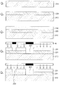
- FIGs. 8 and 9 illustrate processes of manufacturing a printing plate according to an embodiment of the present invention. Processes of manufacturing a printing plate will now be described with reference to Figs. 8 and 9.
- At least one or more photosensitive resin layers are formed on a substrate, and the photosensitive resin layers are patterned to form printing patterns.
- a cleaning process of eliminating contaminants from the substrate 210 is first performed (Q1). Then, a first photosensitive resin layer 220 is formed on the substrate 210 (Q2). For example, a composition for the first photosensitive resin layer is coated on the substrate 210 using spin coating or slit coating and then semi-cured through a thermal treatment.
- a second photosensitive resin layer 230 is formed on the first photosensitive resin layer 220 and then subjected to a thermal treatment (Q3).
- step Q4 the second photosensitive resin layer 230 is exposed to light using a photomask M to form a second pattern 233.
- an upper portion 223a of a first pattern may be formed simultaneously with the formation of the second pattern 233.
- step Q5 the first photosensitive resin layer 230 is exposed to light using a photomask to the first pattern 223 with a width more than a reference width f.
- a printing plate having printing patterns with different widths and depths may be formed.
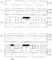
- Fig. 9 illustrates an exemplary process different from the process illustrated in Fig. 8.
- a substrate cleaning process T1 and a first photosensitive resin layer formation process T2 are the same or substantially the same as the steps Q1 and Q2, respectively, as shown in Fig. 8.
- the photosensitive resin layer 220 is patterned using a photomask instead of a second photosensitive resin layer 230, thus forming a lower portion 223b of a first pattern (T3).
- a second photosensitive resin layer 230 is formed on the first photosensitive resin layer 221 and exposed and developed using a photomask to form a second pattern 233 while simultaneously completing the first pattern 223 (T4 and T5).
- the pattern may also be formed using a laser writer.
- Fig. 10 illustrates a structure of a printing plate according to an embodiment of the present invention.
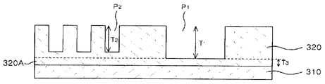
- a printing plate includes a resin layer 320 that has at least one or more printing patterns with different depths.
- the resin layer 320 may include a plurality of printing patterns having different depths T1 and T2, wherein the depth T1 is a depth of a deepest pattern P1.
- the depth T1 of the pattern P1 is formed to be less than a thickness of the resin layer 320 so that a base resin layer 320A with no printing pattern is formed at a lower portion of the resin layer 320.
- the base resin layer 320A may enhance adhesion between the substrate and the resin layer.
- a thickness T3 of the base resin layer may be in a range of 1 to 30um.
- the resin layer 320 may be formed of any one of an epoxy resin, a photosensitive resin, a UV-cured resin, and a thermosetting resin.
- a functional layer (not shown) may be formed of a metal material selected from Cr, Mo, Ta, Ni, and Au, an organic material selected from Parylene and Teflon, or an inorganic material selected from SiOx, SiNx, and diamond-like carbon (DLC), on the resin layer 120 to increase durability of the printing patterns.
- Figs. 11 and 12 illustrate processes of manufacturing a printing plate according to an embodiment of the present invention.
- the present embodiment may focus on a printing plate for manufacturing an electronic substrate and an LCD apparatus.
- the embodiment provides a method of manufacturing a printing plate having at least one or more printing patterns by patterning a resin layer formed on a substrate by an imprinting method, and a structure manufactured by the method.
- a process of manufacturing a printing plate according to the embodiment of the present invention includes forming a resin layer on a substrate and forming printing patterns by performing imprinting on the resin layer with a mold having mold patterns whose depths are different from each other.
- a resin layer 320 is formed on a substrate 310 in step U1.
- any types of materials may be used as the substrate 310 as long as the materials allow for surface flatness, large size, and a similar thermal expansion coefficient even after transfer.
- glass, polymer, such as PC, PMMA, or PET, or metal may be used for the substrate 310.
- the resin layer 320 may be formed of any one of an epoxy photosensitive resin, a polyimide-based photosensitive resin, a UV-cured resin (urethane acrylate, epoxy acrylate, silicon acrylate, polyester acrylate, epoxy vinyl ether, or a thermosetting resin.
- Fig. 13 illustrates an example of using a thermosetting resin
- Fig. 12 illustrates a process of forming the resin layer by applying a UV-cured resin or photosensitive resin liquid by a coating manner.
- the formation of the resin layer by a liquid material, such as the photosensitive resin liquid may be performed by spin coating or slit coating, and various materials, such as a photoresist, a dry film resist, or a UV-cured resin, may be used. Further, any materials having photosensitive characteristics may be used.
- an epoxy-based, polyimide-based, or Novolak-based resin layer may be formed by coating. The subsequent processes are the same and the processes are described with reference to Fig. 11.
- the resin layer 320 is imprinted using a mold 330 having mold patterns with different depths.
- the mold 330 may include a glass mold or a metal mold.
- the metal mold may be formed of Ni, Cr, or Au.
- the depths of the mold patterns are sized so that a base layer 320A is provided at a lower surface of the resin layer 320.
- the resin layer 320 is imprinted so that among the mold patterns having different depths, a mold pattern 131 having a deepest depth does not pass through the resin layer 320, thus leaving a lower layer of the resin layer (hereinafter, referred to as “base resin layer”).
- base resin layer The existence of the base resin layer 320A may enhance adhesion to the substrate 310.
- a thickness of the base resin layer 320A may be in a range of 1 to 30um.
- step U3 the mold 330 is removed from the resin layer 320.
- a functional layer 340 is formed on the resin layer.
- a functional layer (not shown) may be formed of a metal material selected from Cr, Mo, Ta, Ni, and Au, an organic material selected from Parylene and Teflon, or an inorganic material selected from SiOx, SiNx, and diamond-like carbon (DLC), on the resin layer 120 using any one of spin coating, spray coating, sputtering, or CVD.
- the functional layer may increase durability and printability of the printing patterns.
- the functional layer may have the same or substantially the same surface energy as surface energy of a substrate that is subjected to printing.
- an Si-based material having good transfer characteristics such as a-Si, SiNx, or SiOx, may be used.
- the manufacturing process as described above forms patterns by performing imprinting on the photosensitive resin, and accordingly, has merits that micro patterns may be easily formed and the number of processes may be reduced compared to the conventional wet/dry etching methods, thus capable of manufacturing low-cost printing plates. Further, in comparison with an existing method of adjusting the depth of a pattern by randomly not developing a photosensitive resin, the manufacturing process according to the embodiments of the present invention may easily adjust a ratio of a depth and a width of a pattern, may increase uniformity of the depth, and may prevent the printing plate from collapsing at micro pattern regions, thus enhancing durability. Moreover, a single imprinting process may manufacture a printing plate having different depths along pattern widths.
- the base resin layer which is a lower layer of the resin layer may enhance adhesion to the substrate.
- a structure of a printing plate according to an embodiment of the present invention and a method of manufacturing the printing plate will now be described.
- the present embodiment may focus on provision of a printing plate having micro printing patterns, wherein a functional layer is coated on the printing patterns using a photosensitive resin layer to protect the printing patterns and to enhance matching properties of an ink for printing, thus increasing printing quality.
- Fig. 13 illustrates a process of manufacturing a printing plate according to an embodiment of the present invention.
- a printing plate according to an embodiment of the present invention may be manufactured by the following process.
- a photosensitive resin layer is formed on a substrate, printing patterns are formed on the photosensitive resin layer using illumination patterning, and a functional layer is formed on the substrate or the printing patterns.
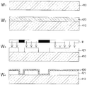
- a substrate 410 is prepared that is used for a printing plate, and a surface of the substrate is cleaned to eliminate contaminants from the substrate.
- Any types of materials may be used as the substrate 410 as long as the materials allow for surface flatness, large size, and a similar thermal expansion coefficient even after transfer.
- glass, polymer, such as PC, PMMA, or PET, or metal may be used for the substrate 410.
- the substrate may have a thermal expansion coefficient that is within four times of a thermal expansion coefficient of a transfer substrate.
- a photosensitive resin layer 420 is formed on the substrate 410.
- the photosensitive resin layer 420 may be formed by coating a resin layer, such as a photoresist resin, a dry film resist film, or a UV-cured resin film, on the substrate 410 followed by semi-curing through a heat treatment.
- a general coating method, such as spin coating or slit coating may be employed.
- step W3 printing patterns are formed by an illumination patterning process.
- the “illumination patterning” refers to forming printing patterns by illuminating the photosensitive resin layer with light beams.
- the illumination patterning process includes processes of forming patterns using photolithography or a laser writer.
- a printing pattern 421 may be formed by exposing and developing the photosensitive resin layer using a photomask M.
- a minimum width of an engraved in the printing pattern 421 may be in a range from 1um to 20um.
- step W4 a functional layer 430 is coated on the printing pattern 421 and exposed surfaces of the substrate.
- the functional layer may be coated using wet coating, such as spray coating or spin coating or dry coating, such as sputtering or CVD.
- dry coating may be performed to prevent contamination and to secure a film uniformity.
- the functional layer 430 may be formed of at least one of various materials, such as, for example, any one or a combination of two or more selected from metal materials, organic or inorganic materials, or hybrid materials of organic and inorganic materials.
- the organic materials may be any one or a combination of two or more selected from Parylene, Teflon, or Polyimide
- the inorganic materials may be any one or a combination of two or more selected from SiOx, SiNx, diamond-like carbon (DLC), TiO 2 , or CeO 2 .
- the hybrid materials may be a composite material obtained by a chemical bond of silane and an alkyl-based resin or a compound obtained by a reaction of alkoxy silane.
- the functional layer 430 protects the printing patterns formed from the photosensitive resin and allows for spreadability of a printing ink.
- Various types of chemicals are used for cleaning the printing plate, and it is impossible to develop a photosensitive resin chemical-resistant against all of the chemicals. Accordingly, by coating a chemical-resistant functional layer on the photosensitive resin layer, the printing patterns may be prevented from being damaged by the chemicals.
- the functional layer also enhances spreadability of a printing ink.
- the surface energy of the printing plate needs to be controlled so that an ink or paste for printing dispersed in various solvents is spread well. Accordingly, matching characteristics may be secured by selecting a material for the functional layer.
- Fig. 14 illustrates a structure of a printing plate according to an embodiment of the present invention.
- a photosensitive resin film having predetermined patterns is formed on a substrate.
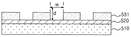
- printing patterns 531 are formed of a photosensitive resin layer on a transparent substrate 510.
- the printing patterns 531 include protruded and depressed patterns.
- the protruded patterns may be formed of an epoxy-based, a polyimide-based, or a Novolak-based material.
- a ratio of the depth d and the width w of the printing patterns may be in a range of (1 ⁇ 4) : 1.
- An adhesive material layer 520 may be provided between the transparent substrate 510 and the printing patterns 531 to increase adhesivity.
- the adhesive material layer may be formed of a photosensitive resin or a metal.
- the adhesive material layer may be formed of any one selected from Au, Ni, Cu, Al, Zn, Fe, Co, W, Sn, P, Cr, or Si, a metal oxide, such as CrOx, CrCOx, or SiOx, or a metal nitride, such as CrN, CrCON, or SiNx.
- a functional layer may be formed on a top of the printing plate.
- the functional layer may be formed of any one or more of Cr, Ni, Au, Parylene, a-Si, SiOx, and SiNx.
- the functional layer may enhance durability and printability of the printing patterns.
- the functional layer may be formed of an Si-based material having good transfer characteristics, such as a-Si, SiNx, or SiOx.
- Figs. 15 and 16 illustrate a process of manufacturing a printing plate according to an embodiment of the present invention.
- the process of manufacturing a printing plate may include forming a photosensitive material layer on a transparent substrate and forming printing patterns by patterning the photosensitive material layer using illumination.
- the process may also include forming a functional layer to enhance durability and printability.
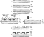
- an adhesive material layer 520 is formed on a substrate 510, and a photosensitive material layer 530 is formed on the adhesive material layer 520.
- the adhesive material layer 520 is formed to increase adhesion between the substrate 510 and the photosensitive material layer 530.
- the substrate 510 may be formed of a transparent material, such as transparent glass.
- the photosensitive material layer 530 may be formed by coating a resin, such as an epoxy-based resin, a polyimide-based resin, or a Novolak-based resin, on the substrate.
- the adhesive material layer 520 may be formed of a photosensitive resin or a metal.
- a low-viscosity photosensitive resin may be coated on the substrate and its overall surface may be exposed to light to form the adhesive material layer.
- illumination patterning refers to a process of forming printing patterns by illuminating the photosensitive material layer with light beams.
- illumination patterning For example, photolithography using a photomask or patterning using a laser writer may be included as examples of the illumination patterning.
- the printing patterns 531 may be formed by exposing and developing processes using a photomask (Z41) or by using a laser writer L2 (Z42).
- a ratio of a depth d and a width w of the printing patterns may be in a range of (1 ⁇ 4) : 1 (refer to Fig. 14).
- a functional layer 540 may be formed on the printing patterns 531 to increase durability and printability.
- the functional layer may be formed of a material having the same surface energy as a substrate on which a printing material is printed.
- the functional layer may be formed of any one or more of Cr, Ni, Au, Parylene, a-Si, SiOx, or SiNx.
- Fig. 16 illustrates actual images of printing patterns in the printing plate shown in Fig. 14.
- the method of manufacturing a printing plate according to the embodiments of the present invention may form elaborate micro printing patterns and a high aspect ratio compared to the method of manufacturing a printing plate by the conventional wet etching.
- the embodiments may address a loss in the minimum width, which occurs upon wet etching, to allow for easy implementation of micro printing patterns and may increase a width of a depth and a width of the micro printing patterns to enhance transfer characteristics of the patterns.
- the processes of manufacturing a printing plate may be simplified to reduce manufacturing costs. Further, since the printing patterns are formed using lithography, a printing plate with high accuracy may be achieved.
- micro printing patterns may be effectively formed, and the number of processes may be reduced to save manufacturing costs. Further, it is possible to easily adjust a ratio of a depth with respect to a width of the patterns, thus enhancing uniformity and preventing the printing plate from collapsing at the printing pattern regions. Accordingly, a printing plate with enhanced durability may be provided.
- micro printing patterns using a printing plate may be performed by an indirect printing method, wherein the printing plate may be used to print various electronic circuits and patterns.
- the printing plate may be used to print various electronic circuits and patterns.
- a printing plate may be formed by performing imprinting on a photosensitive resin and a thermosetting resin using a metal or glass mold. Accordingly, micro patterns having different widths or different depths may be formed with simplified processes, thus lowering manufacturing costs.
- the embodiments of the present invention employ an imprinting process, and thus, a printing plate that includes printing patterns having different depths along the pattern width may be formed by a single process. Due to a base resin layer formed during imprinting, adhesion to the substrate may be increased.
- a functional layer may be formed of a photosensitive resin on printing patterns.
- the functional layer may protect the printing patterns from contaminants and may enhance matching characteristics between a printing ink and the printing patterns to increase printing quality. Further, the functional layer may allow for a printing plate for large-sized micro pattern printing.
Landscapes
- Physics & Mathematics (AREA)
- General Physics & Mathematics (AREA)
- Nonlinear Science (AREA)
- Crystallography & Structural Chemistry (AREA)
- Chemical & Material Sciences (AREA)
- Engineering & Computer Science (AREA)
- Optics & Photonics (AREA)
- Structural Engineering (AREA)
- Architecture (AREA)
- Microelectronics & Electronic Packaging (AREA)
- Mathematical Physics (AREA)
- Printing Plates And Materials Therefor (AREA)
- Materials For Photolithography (AREA)
- Manufacture Or Reproduction Of Printing Formes (AREA)
Abstract
A printing plate is provided comprising a substrate having a first surface and a second surface opposite to the first surface, and a resin layer having a plurality of printing patterns on the first surface of the substrate. A method of manufacturing the printing plate is provided as well. According to the embodiments of the present invention, micro printing patterns may be effectively formed, and the number of processes may be reduced to save manufacturing costs. Further, it is possible to easily adjust a ratio of a depth with respect to a width of the patterns, thus enhancing uniformity and preventing the printing plate from collapsing at the printing pattern regions. Accordingly, a printing plate with enhanced durability may be provided.
Description
This application claims priority to Korean Patent Application No. 10-2010-0068450 filed on July 15, 2010, 10-2010-0068453 filed on July 15, 2010, 10-2010-0069851 filed on July 20, 2010, 10-2010-0072286 filed on July 27, 2010 and 10-2010-0085734 filed on September 1, 2010, the contents of which is hereby incorporated by reference in its entirety into this application.
The embodiments of the present invention are directed to a printing plate for manufacturing an electronic substrate and a display apparatus and a method of manufacturing the printing plate.
Circuits for electronic parts or various patterns may be printed using a direct printing method, such as, for example, inkjet printing, or an indirect printing method, such as, for example, gravure printing or offset printing. For printing, the gravure or offset printing uses a printing plate commonly called “cliche”. A printing plate with a pattern may be manufactured by etching a substrate or by performing photolithography on a plate coated with a photosensitive resin.
In manufacturing a flat-type display apparatus, such as liquid crystal display (LCD) apparatuses, a PR pattern forming process is a critical process that has a great effect on capability of devices for driving the display apparatus, such as thin film transistors (TFTs). Various researches are in progress to enhance capability of the devices, for example, by forming micro metal patterns. In a PR pattern forming process, a photoresist (PR) material is applied as a photosensitive material on a substrate, exposed to light using a mask, and then developed. The PR pattern forming process is, however, too complicate and disadvantage in terms of costs especially when a plurality of patterns are formed for producing the devices because a separate photoresist process needs to be performed for each of the patterns. As an alternative, PR pattern formation using printing has been suggested.
Fig. 1 illustrates a method of manufacturing a printing plate according to a related art.
According to the photoresist printing method as shown in Fig. 1, a photoresist pattern a2 is not directly transferred from a first transparent insulation substrate 110 that has a printing pattern a1 and is used as a printing plate to a second transparent insulation substrate 120 that is subjected to printing. Rather, the photoresist pattern a2 is first transferred to a blanket 100 that has a surface formed of silicon rubber and serves as a medium, and the pattern a2 transferred to the blanket 100 is then transferred to the second transparent insulation substrate 120.
However, the above method cannot achieve a micro line width. To overcome such a problem, a method has been suggested that implements a pattern by photoresist-patterning and then wet-etching a metal film. However, this method suffers from an increased loss in critical dimension (CD) due to batch wet etching, thus rendering it difficult to manufacture an elaborate printing plate with micro patterns.
As the width decreases and the depth increases, that is, a ratio of depth to width increases, a printing pattern etched on a printing plate has better printing characteristics. In the conventional method using wet etching, as the depth increases, the width also increases correspondingly. Thus, it is difficult to manufacture a printing plate with micro patterns and to enhance pattern resolution and transfer characteristics using the conventional method.
Exemplary embodiments of the present invention provide a printing plate and a method of manufacturing the printing plate. According to the embodiments of the present invention, micro printing patterns may be effectively formed, and the number of processes may be reduced to save manufacturing costs. Further, it is possible to easily adjust a ratio of a depth with respect to a width of the patterns, thus enhancing uniformity and preventing the printing plate from collapsing at the printing pattern regions. Accordingly, a printing plate with enhanced durability may be provided.
According to the exemplary embodiments of the present invention, formation of micro printing patterns using a printing plate may be performed by an indirect printing method, wherein the printing plate may be used to print various electronic circuits and patterns. Thus, micro patterns having high accuracy may be formed by simplified processes, thus saving manufacturing costs and enhancing reliability.
According to the exemplary embodiments of the present invention, a printing plate may be formed by performing imprinting on a photosensitive resin and a thermosetting resin using a metal or glass mold. Accordingly, micro patterns having different widths or different depths may be formed with simplified processes, thus lowering manufacturing costs.
According to the exemplary embodiments of the present invention, a functional layer may be formed of a photosensitive resin on printing patterns. The functional layer may protect the printing patterns from contaminants and may enhance matching characteristics between a printing ink and the printing patterns to increase printing quality. Further, the functional layer may allow for a printing plate for large-sized micro pattern printing.
According to an exemplary embodiment of the present invention, there is provided a printing plate comprising a substrate having a first surface and a second surface opposite to the first surface, and a resin layer having a plurality of printing patterns on the first surface of the substrate.
Printing patterns having various structures and high accuracy may be formed by illumination patterning using a photosensitive resin as the resin layer or by laser writing.
As a consequence, printing patterns having uniform shapes or having different depths and widths may be formed. Further, an adhesive layer may be formed to enhance adhesion between the resin layer and the substrate, and a functional layer may be formed on the printing patterns for protection. This provides reliability.
According to the embodiments of the present invention, micro printing patterns may be effectively formed, and the number of processes may be reduced to save manufacturing costs. Further, it is possible to easily adjust a ratio of a depth with respect to a width of the patterns, thus enhancing uniformity and preventing the printing plate from collapsing at the printing pattern regions. Accordingly, a printing plate with enhanced durability may be provided.
According to the exemplary embodiments of the present invention, formation of micro printing patterns using a printing plate may be performed by an indirect printing method, wherein the printing plate may be used to print various electronic circuits and patterns. Thus, micro patterns having high accuracy may be formed by simplified processes, thus saving manufacturing costs and enhancing reliability.
According to the exemplary embodiments of the present invention, a printing plate may be formed by performing imprinting on a photosensitive resin and a thermosetting resin using a metal or glass mold. Accordingly, micro patterns having different widths or different depths may be formed with simplified processes, thus lowering manufacturing costs. In particular, the embodiments of the present invention employ an imprinting process, and thus, a printing plate that includes printing patterns having different depths along the pattern width may be formed by a single process. Due to a base resin layer formed during imprinting, adhesion to the substrate may be increased.
According to the exemplary embodiments of the present invention, a functional layer may be formed of a photosensitive resin on printing patterns. The functional layer may protect the printing patterns from contaminants and may enhance matching characteristics between a printing ink and the printing patterns to increase printing quality. Further, the functional layer may allow for a printing plate for large-sized micro pattern printing.
In particular, compared to the conventional wet etching process, more elaborate micro patterns may be implemented with a high aspect ratio. Further, more simplified processes may be provided than by the conventional dry etching, thus saving manufacturing costs. Plus, a lithography process allows for patterns with higher accuracy.
The embodiments of the present invention will become readily apparent by reference to the following detailed description when considered in conjunction with the accompanying drawings wherein:
Fig. 1 illustrates a method of manufacturing a printing plate according to a related art;
Figs. 2 and 3 illustrate structures of printing plates according to embodiments of the present invention;
Figs. 4 and 5 illustrate a process of manufacturing a printing plate according to an embodiment of the present invention;
Fig. 6 illustrates images of a printing plate actually implemented according to an embodiment of the present invention;
Fig. 7 illustrates a structure of a printing plate according to an embodiment of the present invention;
Figs. 8 and 9 illustrate processes of manufacturing a printing plate according to an embodiment of the present invention;
Fig. 10 illustrates a structure of a printing plate according to an embodiment of the present invention;
Figs. 11 and 12 illustrate processes of manufacturing a printing plate according to an embodiment of the present invention;
Fig. 13 illustrates a process of manufacturing a printing plate according to an embodiment of the present invention;
Fig. 14 illustrates a structure of a printing plate according to an embodiment of the present invention; and
Figs. 15 and 16 illustrate a process of manufacturing a printing plate according to an embodiment of the present invention.
Exemplary embodiments of the present invention will be described with reference to the accompanying drawings, wherein the same reference numerals may be used to denote the same or substantially the same components throughout the specification and the drawings. The terms “first” and “second” may be used to describe various components without limiting the present invention to the terms. The terms may be used only for distinguishing a component from another.
A printing plate according to an embodiment of the present invention includes a first surface and a second surface opposite to the first surface. The first surface of the printing plate includes a resin layer a surface of which has a plurality of printing patterns. Various structures of the printing plate will now be described.
Figs. 2 and 3 illustrate structures of printing plates according to embodiments of the present invention. Referring to Fig. 2, a printing plate includes first and second printing patterns 123 and 132 formed by patterning a photosensitive resin layer 120 deposited on a substrate 110. The first and second printing patterns 123 and 132 have different depths and different widths from each other. The first printing pattern 123 is a reference pattern, and the second pattern 132 is a minimum pattern. According to an embodiment, more printing patterns that those illustrated in Fig. 2 may be formed that have different depths and widths from one another.
According to an embodiment, a ratio of a line width and a depth of a printing pattern may be in a range of 1 : (0.5~4).
Although it has been illustrated that a depth of the first pattern 123 is the same as a thickness of the photosensitive resin layer 120, the embodiments of the present invention are not limited thereto, and according to an embodiment, the depth of the first pattern 123 may be less than the thickness of the photosensitive resin layer 120. According to an embodiment, a depth of the second pattern 132 may be less than the thickness of the photosensitive resin layer 120. According to an embodiment, the depth d1 and the width w1 of the first pattern 123 may be more than the depth d2 and the width w2 of the second pattern 132.
According to an embodiment, a functional layer 140 may be formed of a metal material selected from Cr, Mo, Ta, and Ni, an organic material selected from Parylene and Teflon, or an inorganic material selected from SiOx, SiNx, and diamond-like carbon (DLC), on the substrate 110 and the printing patterns 123 and 132.
The structure shown in Fig. 3 is identical in material and printing patterns to the structure shown in Fig. 2 except for the structure of the first pattern 123. This characteristic difference in structure may originate from a manufacturing process shown in Fig. 5.
In a process of first forming a lower portion of the first pattern and then the second pattern, the first pattern 123 is formed so that a width W1 of the upper portion is larger than a width W1’ of the lower portion to maximize alignment efficiency. According to an embodiment, a difference between the width W1 and the widths W1’ may be in a range of 5 to 20um.
Figs. 4 and 5 illustrate a process of manufacturing a printing plate according to an embodiment of the present invention.
Referring to Figs. 4 and 5, a process of manufacturing a printing plate will be described.
The manufacturing process may be implemented in various manners depending on methods of forming a photosensitive resin layer on a substrate and forming a printing pattern on the resin layer.
Referring to Fig. 4, the manufacturing process includes applying a first photosensitive resin on a substrate and exposing to light to thereby form a lower portion of a first pattern, applying a second photosensitive resin on the first photosensitive resin and exposing to light to form an upper portion of the first pattern and a second pattern, and simultaneously developing the first and second photosensitive resins to form the first and second patterns.
For example, the printing patterns may be complete by performing application of the photosensitive resin and exposure to light at the same time and by performing batch development after the formation of the second pattern. However, the embodiments of the present invention are not limited thereto. According to an embodiment, exposing and developing steps may be separately conducted for each photosensitive resin layer to form the printing patterns.
In step S1, a photosensitive resin is applied on a substrate 110 to form a first photosensitive resin layer 120.
Any types of materials may be used as the substrate 110 as long as the materials allow for surface flatness, large size, and a similar thermal expansion coefficient even after transfer. For example, according to an embodiment, glass, polymer, such as PC, PMMA, or PET, or metal may be used for the substrate 110.
According to an embodiment, the photosensitive resin may be formed using general spin coating or slit coating. Various materials, such as photoresists, dry film resists, or UV cured resins, may be used as the photosensitive resin. Besides, any materials having photosensitive characteristics, such as, for example, epoxy-based, polyimide-based, Novolak-based resins, may also be employed as the photosensitive resin.
Thereafter, in step S2, the first photosensitive resin layer 120 is exposed to light to form the lower portion 121 of the first pattern. A laser writer L may be used for patterning. According to an embodiment, the lower portion of the first pattern may be complete by performing development immediately after patterning by exposure to light. In the present embodiment, however, the exposing step may also be performed. Although it has been described in the present embodiment that a negative photosensitive material is used that forms a pattern at a portion that is not illuminated with a laser beam. According to an embodiment, a positive photosensitive material may also be used that forms a pattern in a manner opposite to that of the negative photosensitive material.
In step S3, a photosensitive material is applied on the patterned first photosensitive resin layer to form a second photosensitive resin layer 130.
Thereafter, in step S4, second exposure to light is performed on the second photosensitive resin layer 130 to pattern a second pattern 131 and an upper portion 122 of the first pattern.
In step S5, if portions not exposed to light are simultaneously removed (developed), a printing plate is complete that has the first and second patterns 123 and 132. As shown in Fig. 4, the first pattern 123 has larger width and depth than those of the second pattern 132. According to an embodiment, a ratio of the width to the depth of each of the first and second patterns may be in a range 1 : (0.5~1.4).
In step S6, a function layer 140 may be formed on the first and second patterns. The function layer 140 may be formed of a a metal material selected from Cr, Mo, Ta, and Ni, an organic material selected from Parylene and Teflon, or an inorganic material selected from SiOx, SiNx, and diamond-like carbon (DLC), using one selected from spin coating, spray coating, sputtering, and chemical vapor deposition (CVD). The functional layer 140 may enhance durability and printing characteristics of the printing patterns. According to an embodiment, the function layer 140 may be formed of a material, such as a-Si, SiNx, or SiOx.
The manufacturing process as described above forms patterns by performing photolithography on the photosensitive resin, and accordingly, has merits that micro patterns may be easily formed and the number of processes may be reduced compared to the conventional wet/dry etching methods, thus capable of manufacturing low-cost printing plates. Further, in comparison with an existing method of adjusting the depth of a pattern by randomly not developing a photosensitive resin, the manufacturing process according to the embodiments of the present invention may easily adjust a ratio of a depth and a width of a pattern, may increase uniformity of the depth, and may prevent the printing plate from collapsing at micro pattern regions, thus enhancing durability.
Fig. 5 illustrates a process of manufacturing a printing plate according to an embodiment of the present invention.
Referring to Fig. 5, in the present manufacturing process, an exposing process is performed using a photomask unlike the embodiment described in connection with Fig. 4 that performs patterning through exposure of the photosensitive resin layer to light.
Specifically, in step P1, a first photosensitive material layer 120 is formed on a substrate 110. In step P2, a lower portion 121 of a first pattern is formed by an exposure system (e.g., UV exposure system) through the medium of a photomask. In step P3, a second photosensitive material layer 130 is formed on the lower portion 121 and the layer 120. Then, an upper portion 122 of the first pattern and a second pattern 131 are patterned using a photomask M. In performing exposure to light, an alignment between patterns is critical. Thus, according to an embodiment, the lower portion 121 of the first pattern may be designed to be smaller than the upper portion 122 of the first pattern to enhance a process margin.
Then, in step P5, the first and second photosensitive material layers are exposed to light at the same time to complete first and second patterns 123 and 132. As shown in Fig. 5, in a case where the lower portion of the first pattern is designed to be narrower than the upper portion of the first pattern in step P4 for alignment efficiency, predetermined step portions Q are formed in the first pattern 123. In this case, there is a difference in width between the upper and lower portions of the first pattern. For example, the lower portion is formed to be narrower than the upper portion. The difference in width may range from 5 to 20um.
Thereafter, in step P6, a functional layer 140 is formed, thus completing a printing plate. In the present embodiment, the first pattern 123 is formed to have larger width and depth than those of the second pattern 132. According to an embodiment, like the embodiment described in connection with Fig. 3, a ratio of a width and a depth of each pattern may be in a range of 1 : (0.5~1.4). According to embodiments, processes, materials, and photosensitive materials for forming the functional layer may be the same as those of the embodiment described in connection with Fig. 3, and thus, repetitive description thereof will be omitted.
Fig. 6 illustrates images of a printing plate actually implemented according to an embodiment of the present invention.
The method of manufacturing a printing plate according to the embodiments of the present invention may configure micro patterns more efficiently than the conventional method of manufacturing a printing plate using wet etching, and may implement a high A/R (Aspect Ratio). The method according to the embodiments of the present invention may solve problems of a minimum width loss that occurs upon performing the conventional wet etching so that micro patterns may be easily implemented, and may considerably increase a ratio of a width and a depth of each micro pattern to enhance transfer characteristics.
Further, the method of manufacturing a printing plate according to the embodiments of the present invention may simplify the steps of implementing a printing plate compared to a method of manufacturing a printing plate by performing dry etching on a material film for dry etching, and may save manufacturing costs. Further, the method according to the embodiments of the present invention forms printing patterns using lithography, and thus, high patterning accuracy may be achieved.
Specifically, since printing patterns are formed by patterning a photosensitive resin, micro patterns may be efficiently formed, and the number of processes may be reduced, thus saving manufacturing costs. Further, a ratio of a depth with respect to a width of each pattern may be easily adjusted, and depth uniformity may be raised. Accordingly, it may be possible to prevent the printing plate from collapsing at micro pattern regions, thus allowing for a durable printing plate.
Fig. 7 illustrates a structure of a printing plate according to an embodiment of the present invention.
Referring to Fig. 7, a printing plate includes photosensitive resin layers 221 and 231 formed on a substrate 210, and a plurality of printing patterns 223 and 233 formed by patterning the photosensitive resin layers and having different widths and depths from each other.
Any types of materials may be used as the substrate 110 as long as the materials allow for surface flatness, large size, and a similar thermal expansion coefficient even after transfer. For example, according to an embodiment, glass, polymer, such as PC, PMMA, or PET, or metal may be used for the substrate 110. For maintaining accuracy of the patterns, the substrate may have a thermal expansion coefficient that is within two times of a thermal expansion coefficient of a transfer substrate.
Although it has been described that two photosensitive resin layers 221 and 231 are formed, the embodiments of the present invention are not limited thereto. According to embodiments, more than two photosensitive resin layers may be formed that include printing patterns at least two of which have different depths from each other. In the present embodiment, the photosensitive resin layer formed on the substrate is referred to as “first photosensitive resin layer 221” and the other photosensitive resin layer formed on the first photosensitive resin layer 221 is referred to as “second photosensitive resin layer 231”. According to an embodiment, the first and second photosensitive resin layers may be formed using general spin coating or slit coating. Various materials, such as photoresists, dry film resists, or UV cured resins, may be used as the first and second photosensitive resin layers. Further, any materials having photosensitive characteristics may also be employed as the first and second photosensitive resin layers.
At least two or more printing patterns, such as the printing patterns 223 and 233, which have different widths and depths, may be formed by patterning the photosensitive resin layers 221 and 231. According to an embodiment, at least one first pattern 223 having a reference width f and at least one second pattern 233 having a minimum micro pattern width e may be included, wherein the reference width f refers to a width of a pattern formed on the substrate. According to an embodiment, a depth of the second pattern may be formed to be less than a depth of the first pattern.
The second pattern 233 may be formed in the second photosensitive resin layer 231. Although it has been shown that a thickness T1 of the second pattern 233 is the same as a thickness d of the second photosensitive resin layer 231, the thickness T1 may be smaller than the thickness d of the second photosensitive resin layer 231.
The width e of the second pattern 233 and the thickness d of the second photosensitive resin layer 131 satisfy the following Equation 1:
[Equation 1]
d≥½*e
According to an embodiment, the thickness d of the second photosensitive resin layer may be formed to be larger than the width e of the second pattern 233 by more than 50%. In other words, the second photosensitive resin layer may be formed to have a thickness more than two times of the width e of the second pattern 233.
The first pattern 223 may be formed in the first and second photosensitive resin layers. The first pattern 223 is formed to be deeper than the second pattern 233. Although it has been illustrated in Fig. 7 that a depth T2 of the second pattern 233 is the same as a sum of thicknesses of the first and second photosensitive resin layers, the depth T2 of the second pattern 233 may be formed to be less than the sum of the thicknesses of the first and second photosensitive resin layers.
The thickness c of the first photosensitive resin layer with respect to the thickness d of the second photosensitive resin layer and the width e of the second pattern satisfies the following Equation 2:
[Equation 2]
c≥d-½*e
According to an embodiment, the thickness c of the first photosensitive resin layer 221 may be formed to be larger than a difference between the thickness d of the second photosensitive resin layer and a half of the width e of the second pattern.
According to an embodiment, the width e of the second pattern may be in a range of 1 to 50um, for example, 5 to 25um.
According to an embodiment, the thickness d of the second photosensitive resin layer may range from 2.5 to 12.5um, and the thickness c of the first photosensitive resin layer may be equal to or more than 1.25um.
The first pattern with the width f may be formed as a reference pattern in the first and second photosensitive resin layers, and the second pattern with the width e may be formed in the second photosensitive resin layer, wherein the second pattern is smaller than the first pattern. The width f of the first pattern and the width e of the second pattern satisfy the following Equation 3:
f≥1.5×e
Figs. 8 and 9 illustrate processes of manufacturing a printing plate according to an embodiment of the present invention. Processes of manufacturing a printing plate will now be described with reference to Figs. 8 and 9.
Referring to Fig. 8, at least one or more photosensitive resin layers are formed on a substrate, and the photosensitive resin layers are patterned to form printing patterns.
Specifically, a cleaning process of eliminating contaminants from the substrate 210 is first performed (Q1). Then, a first photosensitive resin layer 220 is formed on the substrate 210 (Q2). For example, a composition for the first photosensitive resin layer is coated on the substrate 210 using spin coating or slit coating and then semi-cured through a thermal treatment.
Next, a second photosensitive resin layer 230 is formed on the first photosensitive resin layer 220 and then subjected to a thermal treatment (Q3).
In step Q4, the second photosensitive resin layer 230 is exposed to light using a photomask M to form a second pattern 233. According to an embodiment, an upper portion 223a of a first pattern may be formed simultaneously with the formation of the second pattern 233.
In step Q5, the first photosensitive resin layer 230 is exposed to light using a photomask to the first pattern 223 with a width more than a reference width f.
Through the above-described processes, a printing plate having printing patterns with different widths and depths may be formed.
Fig. 9 illustrates an exemplary process different from the process illustrated in Fig. 8.
Referring to Fig. 9, a substrate cleaning process T1 and a first photosensitive resin layer formation process T2 are the same or substantially the same as the steps Q1 and Q2, respectively, as shown in Fig. 8. As shown in Fig. 9, the photosensitive resin layer 220 is patterned using a photomask instead of a second photosensitive resin layer 230, thus forming a lower portion 223b of a first pattern (T3).
Thereafter, a second photosensitive resin layer 230 is formed on the first photosensitive resin layer 221 and exposed and developed using a photomask to form a second pattern 233 while simultaneously completing the first pattern 223 (T4 and T5).
Although it has been described to perform exposure and development using the photomask while forming the patterns, the pattern may also be formed using a laser writer.
Fig. 10 illustrates a structure of a printing plate according to an embodiment of the present invention.
Referring to Fig. 10, a printing plate includes a resin layer 320 that has at least one or more printing patterns with different depths. For example, the resin layer 320 may include a plurality of printing patterns having different depths T1 and T2, wherein the depth T1 is a depth of a deepest pattern P1. The depth T1 of the pattern P1 is formed to be less than a thickness of the resin layer 320 so that a base resin layer 320A with no printing pattern is formed at a lower portion of the resin layer 320. The base resin layer 320A may enhance adhesion between the substrate and the resin layer. According to an embodiment, a thickness T3 of the base resin layer may be in a range of 1 to 30um.
According to an embodiment, the resin layer 320 may be formed of any one of an epoxy resin, a photosensitive resin, a UV-cured resin, and a thermosetting resin. According to an embodiment, a functional layer (not shown) may be formed of a metal material selected from Cr, Mo, Ta, Ni, and Au, an organic material selected from Parylene and Teflon, or an inorganic material selected from SiOx, SiNx, and diamond-like carbon (DLC), on the resin layer 120 to increase durability of the printing patterns.
Figs. 11 and 12 illustrate processes of manufacturing a printing plate according to an embodiment of the present invention.
The present embodiment may focus on a printing plate for manufacturing an electronic substrate and an LCD apparatus. In particular, the embodiment provides a method of manufacturing a printing plate having at least one or more printing patterns by patterning a resin layer formed on a substrate by an imprinting method, and a structure manufactured by the method.
Referring to Figs. 11 and 12, a process of manufacturing a printing plate according to the embodiment of the present invention includes forming a resin layer on a substrate and forming printing patterns by performing imprinting on the resin layer with a mold having mold patterns whose depths are different from each other.
Specifically, as shown in Fig. 11, a resin layer 320 is formed on a substrate 310 in step U1.
Any types of materials may be used as the substrate 310 as long as the materials allow for surface flatness, large size, and a similar thermal expansion coefficient even after transfer. For example, according to an embodiment, glass, polymer, such as PC, PMMA, or PET, or metal may be used for the substrate 310.
The resin layer 320 may be formed of any one of an epoxy photosensitive resin, a polyimide-based photosensitive resin, a UV-cured resin (urethane acrylate, epoxy acrylate, silicon acrylate, polyester acrylate, epoxy vinyl ether, or a thermosetting resin. Fig. 13 illustrates an example of using a thermosetting resin, and Fig. 12 illustrates a process of forming the resin layer by applying a UV-cured resin or photosensitive resin liquid by a coating manner. The formation of the resin layer by a liquid material, such as the photosensitive resin liquid, may be performed by spin coating or slit coating, and various materials, such as a photoresist, a dry film resist, or a UV-cured resin, may be used. Further, any materials having photosensitive characteristics may be used. For example, an epoxy-based, polyimide-based, or Novolak-based resin layer may be formed by coating. The subsequent processes are the same and the processes are described with reference to Fig. 11.
In step U2, the resin layer 320 is imprinted using a mold 330 having mold patterns with different depths. The mold 330 may include a glass mold or a metal mold. The metal mold may be formed of Ni, Cr, or Au.
According to an embodiment, the depths of the mold patterns are sized so that a base layer 320A is provided at a lower surface of the resin layer 320. For example, the resin layer 320 is imprinted so that among the mold patterns having different depths, a mold pattern 131 having a deepest depth does not pass through the resin layer 320, thus leaving a lower layer of the resin layer (hereinafter, referred to as “base resin layer”). The existence of the base resin layer 320A may enhance adhesion to the substrate 310. According to an embodiment, a thickness of the base resin layer 320A may be in a range of 1 to 30um.
In step U3, the mold 330 is removed from the resin layer 320.
In step U4, a functional layer 340 is formed on the resin layer. According to an embodiment, a functional layer (not shown) may be formed of a metal material selected from Cr, Mo, Ta, Ni, and Au, an organic material selected from Parylene and Teflon, or an inorganic material selected from SiOx, SiNx, and diamond-like carbon (DLC), on the resin layer 120 using any one of spin coating, spray coating, sputtering, or CVD. The functional layer may increase durability and printability of the printing patterns. Accordingly, the functional layer may have the same or substantially the same surface energy as surface energy of a substrate that is subjected to printing. For example, an Si-based material having good transfer characteristics, such as a-Si, SiNx, or SiOx, may be used.
The manufacturing process as described above forms patterns by performing imprinting on the photosensitive resin, and accordingly, has merits that micro patterns may be easily formed and the number of processes may be reduced compared to the conventional wet/dry etching methods, thus capable of manufacturing low-cost printing plates. Further, in comparison with an existing method of adjusting the depth of a pattern by randomly not developing a photosensitive resin, the manufacturing process according to the embodiments of the present invention may easily adjust a ratio of a depth and a width of a pattern, may increase uniformity of the depth, and may prevent the printing plate from collapsing at micro pattern regions, thus enhancing durability. Moreover, a single imprinting process may manufacture a printing plate having different depths along pattern widths. The base resin layer which is a lower layer of the resin layer may enhance adhesion to the substrate.
A structure of a printing plate according to an embodiment of the present invention and a method of manufacturing the printing plate will now be described.
The present embodiment may focus on provision of a printing plate having micro printing patterns, wherein a functional layer is coated on the printing patterns using a photosensitive resin layer to protect the printing patterns and to enhance matching properties of an ink for printing, thus increasing printing quality.
Fig. 13 illustrates a process of manufacturing a printing plate according to an embodiment of the present invention.
Referring to Fig. 13, a printing plate according to an embodiment of the present invention may be manufactured by the following process.
To manufacture the printing plate, a photosensitive resin layer is formed on a substrate, printing patterns are formed on the photosensitive resin layer using illumination patterning, and a functional layer is formed on the substrate or the printing patterns.
Specifically, in step W1, a substrate 410 is prepared that is used for a printing plate, and a surface of the substrate is cleaned to eliminate contaminants from the substrate. Any types of materials may be used as the substrate 410 as long as the materials allow for surface flatness, large size, and a similar thermal expansion coefficient even after transfer. For example, according to an embodiment, glass, polymer, such as PC, PMMA, or PET, or metal may be used for the substrate 410. For maintaining accuracy of the patterns, the substrate may have a thermal expansion coefficient that is within four times of a thermal expansion coefficient of a transfer substrate.
Next, in step W2, a photosensitive resin layer 420 is formed on the substrate 410. In general, the photosensitive resin layer 420 may be formed by coating a resin layer, such as a photoresist resin, a dry film resist film, or a UV-cured resin film, on the substrate 410 followed by semi-curing through a heat treatment. A general coating method, such as spin coating or slit coating may be employed.
In step W3, printing patterns are formed by an illumination patterning process.
The “illumination patterning” refers to forming printing patterns by illuminating the photosensitive resin layer with light beams. For example, the illumination patterning process includes processes of forming patterns using photolithography or a laser writer. As shown in Fig. 13, a printing pattern 421 may be formed by exposing and developing the photosensitive resin layer using a photomask M. According to an embodiment, a minimum width of an engraved in the printing pattern 421 may be in a range from 1um to 20um.
Thereafter, in step W4, a functional layer 430 is coated on the printing pattern 421 and exposed surfaces of the substrate.
The functional layer may be coated using wet coating, such as spray coating or spin coating or dry coating, such as sputtering or CVD. According to an embodiment, dry coating may be performed to prevent contamination and to secure a film uniformity.
Depending on features of the photosensitive resin layer and the substrate, the functional layer 430 may be formed of at least one of various materials, such as, for example, any one or a combination of two or more selected from metal materials, organic or inorganic materials, or hybrid materials of organic and inorganic materials. For example, the organic materials may be any one or a combination of two or more selected from Parylene, Teflon, or Polyimide, the inorganic materials may be any one or a combination of two or more selected from SiOx, SiNx, diamond-like carbon (DLC), TiO2, or CeO2. The hybrid materials may be a composite material obtained by a chemical bond of silane and an alkyl-based resin or a compound obtained by a reaction of alkoxy silane.
The functional layer 430 protects the printing patterns formed from the photosensitive resin and allows for spreadability of a printing ink. Various types of chemicals are used for cleaning the printing plate, and it is impossible to develop a photosensitive resin chemical-resistant against all of the chemicals. Accordingly, by coating a chemical-resistant functional layer on the photosensitive resin layer, the printing patterns may be prevented from being damaged by the chemicals.
As described above, the functional layer also enhances spreadability of a printing ink. The surface energy of the printing plate needs to be controlled so that an ink or paste for printing dispersed in various solvents is spread well. Accordingly, matching characteristics may be secured by selecting a material for the functional layer.
Fig. 14 illustrates a structure of a printing plate according to an embodiment of the present invention.
Referring to Fig. 14, a photosensitive resin film having predetermined patterns is formed on a substrate. Specifically, printing patterns 531 are formed of a photosensitive resin layer on a transparent substrate 510. The printing patterns 531 include protruded and depressed patterns. The protruded patterns may be formed of an epoxy-based, a polyimide-based, or a Novolak-based material.
According to an embodiment, a ratio of the depth d and the width w of the printing patterns may be in a range of (1~4) : 1. An adhesive material layer 520 may be provided between the transparent substrate 510 and the printing patterns 531 to increase adhesivity. According to an embodiment, the adhesive material layer may be formed of a photosensitive resin or a metal.
Specifically, the adhesive material layer may be formed of any one selected from Au, Ni, Cu, Al, Zn, Fe, Co, W, Sn, P, Cr, or Si, a metal oxide, such as CrOx, CrCOx, or SiOx, or a metal nitride, such as CrN, CrCON, or SiNx.
According to an embodiment, a functional layer may be formed on a top of the printing plate. The functional layer may be formed of any one or more of Cr, Ni, Au, Parylene, a-Si, SiOx, and SiNx. The functional layer may enhance durability and printability of the printing patterns. According to an embodiment, the functional layer may be formed of an Si-based material having good transfer characteristics, such as a-Si, SiNx, or SiOx.
Figs. 15 and 16 illustrate a process of manufacturing a printing plate according to an embodiment of the present invention.
The process of manufacturing a printing plate may include forming a photosensitive material layer on a transparent substrate and forming printing patterns by patterning the photosensitive material layer using illumination. The process may also include forming a functional layer to enhance durability and printability.
The process will be described in detail with reference to Fig. 15.
In steps Z1 to Z3, an adhesive material layer 520 is formed on a substrate 510, and a photosensitive material layer 530 is formed on the adhesive material layer 520. The adhesive material layer 520 is formed to increase adhesion between the substrate 510 and the photosensitive material layer 530.
According to an embodiment, the substrate 510 may be formed of a transparent material, such as transparent glass.
According to an embodiment, the photosensitive material layer 530 may be formed by coating a resin, such as an epoxy-based resin, a polyimide-based resin, or a Novolak-based resin, on the substrate. According to an embodiment, the adhesive material layer 520 may be formed of a photosensitive resin or a metal. For example, a low-viscosity photosensitive resin may be coated on the substrate and its overall surface may be exposed to light to form the adhesive material layer.
Thereafter, the photosensitive material layer 530 is subjected to illumination patterning to form printing patterns 531. The “illumination patterning” refers to a process of forming printing patterns by illuminating the photosensitive material layer with light beams. For example, photolithography using a photomask or patterning using a laser writer may be included as examples of the illumination patterning.
For example, the printing patterns 531 may be formed by exposing and developing processes using a photomask (Z41) or by using a laser writer L2 (Z42). According to an embodiment, considering protruded patterns and depressed patterns in the printing patterns 531, a ratio of a depth d and a width w of the printing patterns may be in a range of (1~4) : 1 (refer to Fig. 14).
Thereafter, a functional layer 540 may be formed on the printing patterns 531 to increase durability and printability. According to an embodiment, the functional layer may be formed of a material having the same surface energy as a substrate on which a printing material is printed. For example, the functional layer may be formed of any one or more of Cr, Ni, Au, Parylene, a-Si, SiOx, or SiNx.
Fig. 16 illustrates actual images of printing patterns in the printing plate shown in Fig. 14.
The method of manufacturing a printing plate according to the embodiments of the present invention may form elaborate micro printing patterns and a high aspect ratio compared to the method of manufacturing a printing plate by the conventional wet etching. For example, the embodiments may address a loss in the minimum width, which occurs upon wet etching, to allow for easy implementation of micro printing patterns and may increase a width of a depth and a width of the micro printing patterns to enhance transfer characteristics of the patterns.
In comparison with the convention method of manufacturing a printing plate by dry etching, the processes of manufacturing a printing plate may be simplified to reduce manufacturing costs. Further, since the printing patterns are formed using lithography, a printing plate with high accuracy may be achieved.
According to the embodiments of the present invention, micro printing patterns may be effectively formed, and the number of processes may be reduced to save manufacturing costs. Further, it is possible to easily adjust a ratio of a depth with respect to a width of the patterns, thus enhancing uniformity and preventing the printing plate from collapsing at the printing pattern regions. Accordingly, a printing plate with enhanced durability may be provided.
According to the exemplary embodiments of the present invention, formation of micro printing patterns using a printing plate may be performed by an indirect printing method, wherein the printing plate may be used to print various electronic circuits and patterns. Thus, micro patterns having high accuracy may be formed by simplified processes, thus saving manufacturing costs and enhancing reliability.
According to the exemplary embodiments of the present invention, a printing plate may be formed by performing imprinting on a photosensitive resin and a thermosetting resin using a metal or glass mold. Accordingly, micro patterns having different widths or different depths may be formed with simplified processes, thus lowering manufacturing costs. In particular, the embodiments of the present invention employ an imprinting process, and thus, a printing plate that includes printing patterns having different depths along the pattern width may be formed by a single process. Due to a base resin layer formed during imprinting, adhesion to the substrate may be increased.
According to the exemplary embodiments of the present invention, a functional layer may be formed of a photosensitive resin on printing patterns. The functional layer may protect the printing patterns from contaminants and may enhance matching characteristics between a printing ink and the printing patterns to increase printing quality. Further, the functional layer may allow for a printing plate for large-sized micro pattern printing.
In particular, compared to the conventional wet etching process, more elaborate micro patterns may be implemented with a high aspect ratio. Further, more simplified processes may be provided than by the conventional dry etching, thus saving manufacturing costs. Plus, a lithography process allows for patterns with higher accuracy.
The invention has been explained above with reference to exemplary embodiments. It will be evident to those skilled in the art that various modifications may be made thereto without departing from the broader spirit and scope of the invention. Further, although the invention has been described in the context its implementation in particular environments and for particular applications, those skilled in the art will recognize that the present invention's usefulness is not limited thereto and that the invention can be beneficially utilized in any number of environments and implementations. The foregoing description and drawings are, accordingly, to be regarded in an illustrative rather than a restrictive sense.
Claims (39)
- A printing plate comprising:a substrate having a first surface and a second surface opposite to the first surface; anda resin layer having a plurality of printing patterns on the first surface of the substrate.
- The printing plate of claim 1, wherein the resin layer is formed of any one of a photoresist, a dry film resist (DFR), a UV-cured resin, an epoxy resin, and a thermosetting resin.
- The printing plate of claim 2, wherein the printing patterns have different depths or widths.
- The printing plate of claim 3, wherein the printing patterns include at least one reference pattern and at least one minimum pattern.
- The printing plate of claim 4, wherein a depth and a width of the reference pattern are larger than a depth and a width of the minimum pattern, respectively.
- The printing plate of claim 4, wherein a ratio of a width and a depth of the printing patterns are in a range of 1 : (0.5~4).
- The printing plate of claim 4, wherein a width W1 of an upper portion of the reference pattern is larger than a width W1’ of a lower portion of the reference pattern.
- The printing plate of claim 4, wherein a difference between a width W1 of an upper portion of the reference pattern and a width W1’ of a lower portion of the reference pattern ranges from 5um to 20um.
- The printing plate of claim 1 or 4, further comprising:a functional layer on an exposed surface of the substrate or the printing patterns.
- The printing plate of claim 9, wherein the functional layer is formed of any one or a combination of two or more selected from metal materials including Cr, Mo, Ta, Ni, or Al, any one or a combination of two or more selected from organic materials including Parylene, Teflon, or Polyimide, any one or a combination of two or more selected from inorganic materials including SiOx, SiNx, diamond-like carbon (DLC), TiO2, or CeO2, a composite material obtained by a chemical bond of silane and an alkyl-based resin, or a compound obtained by a reaction of alkoxy silane.
- The printing plate of claim 4, wherein the resin layer includes at least two or more stacked photosensitive layers.
- The printing plate of claim 11, wherein a depth of the minimum pattern is less than a depth of the reference pattern.
- The printing plate of claim 12, wherein the minimum pattern is formed in a second photosensitive resin layer and wherein a thickness d of the second photosensitive resin layer and a width e of the minimum pattern satisfy following Equation 1:[Equation 1]d≥½*e
- The printing plate of claim 12, wherein the reference pattern is formed in first and second photosensitive resin layers and wherein a thickness c of the first photosensitive resin layer satisfies following Equation 2:[Equation 2]c≥d-½*e(where, d refers to a thickness of the second photosensitive resin layer and e refers to a width of the minimum pattern)
- The printing plate of claim 12, wherein a width f of the reference pattern satisfies following Equation 3:[Equation 3]f≥1.5*e(where, e refers to a width of the minimum pattern)
- The printing plate of claim 12, wherein a width e of the minimum pattern ranges from 1um to 50um.
- The printing plate of clam 12, wherein a thickness c of the first photosensitive resin layer is more than 1.25um, and a thickness d of the second photosensitive resin layer ranges from 2.5um to 12.5um.
- The printing plate of claim 1, wherein the resin layer includes a base resin layer where no printing patterns are formed, and wherein a thickness of the base resin layer ranges from 1um to 30um.
- The printing plate of claim 18, further comprising:a functional layer on the printing patterns, wherein the functional layer is formed of any one or a combination of two or more selected from metal materials including Cr, Mo, Ta, Ni, or Al, any one or a combination of two or more selected from organic materials including Parylene, Teflon, or Polyimide, any one or a combination of two or more selected from inorganic materials including SiOx, SiNx, diamond-like carbon (DLC), TiO2, or CeO2, a composite material obtained by a chemical bond of silane and an alkyl-based resin, or a compound obtained by a reaction of alkoxy silane.
- The printing plate of claim 1, further comprising:an adhesive material layer between the substrate and the resin layer, wherein the resin layer is a photosensitive material layer.
- The printing plate of claim 20, wherein the adhesive material layer is formed of a photosensitive resin, any one metal material selected from Au, Ni, Cu, Al, Zn, Fe, Co, W, Sn, P, Cr, and Si, an oxide of the selected metal material, or a nitride of the selected metal material.
- The printing plate of claim 20, wherein a ratio of a depth d and a width w of the printing patterns is in a range of (1~4) : 1.
- A method of manufacturing a printing plate comprising:forming a lower portion of a first pattern by applying a first photosensitive resin on a substrate and by exposing the first photosensitive resin;forming an upper portion of the first pattern and a second pattern by applying a second photosensitive resin on the first photosensitive resin and by exposing the second photosensitive resin; andforming the first and second patterns by simultaneously developing the first and second photosensitive resins.
- A method of manufacturing a printing plate comprising:forming a lower portion of a first pattern by applying a first photosensitive resin on a substrate and by exposing and developing the first photosensitive resion; andforming an upper portion of the first pattern and a second pattern by applying a second photosensitive resin on the first photosensitive resin and by exposing and developing the second photosensitive resin.
- The method of claim 23 or 24, further comprising:forming a functional layer on the first and second patterns.
- The method of claim 25, wherein developing is performed such that a width of the lower portion of the first pattern is narrower than a width of the upper portion of the first pattern.
- The method of claim 25, wherein forming the first pattern or the second pattern is performed such that a ratio of a width and a depth of each pattern is in a range of 1 : (0.5~1.4).
- A method of manufacturing a printing plate comprising:forming at least one resin layer on a substrate; andforming a plurality of printing patterns by patterning the resin layer.
- The method of claim 28, wherein the plurality of printing patterns have different depths and widths from each other.
- The method of claim 29, wherein forming the plurality of printing patterns includes,forming first and second photosensitive resin layers on the substrate, wherein the resin layer includes the first and second photosensitive resin layers, andforming at least one reference pattern and at least one minimum pattern by exposure to light.
- The method of claim 30, wherein forming the plurality of printing patterns includes,forming the first photosensitive resin layer on the substrate and forming the reference pattern by exposure to light, andforming the second photosensitive resin layer on the first photosensitive resin layer and forming the minimum pattern by exposure to light and development.
- The method of claim 29 or 30, wherein a depth of the minimum pattern is less than a depth of the reference pattern.
- The method of claim 28, wherein forming the plurality of printing patterns is performed by illumination patterning, wherein the resin layer is a photosensitive resin layer.
- The method of claim 28, wherein forming the plurality of printing patterns is performed by imprinting the resin layer using a mold having mold patterns whose depths are different from each other.
- The method of claim 34, wherein the printing patterns include at least one or more that have different depths from each other, and wherein a base resin layer is formed at a lower portion of the resin layer to have a thickness of 1 to 30um, and wherein no printing patterns are formed in the base resin layer.
- The method of claim 33 or 34, further comprising:forming a functional layer on the substrate or the printing plate.
- The method of claim 28, further comprising:forming an adhesive material layer between the substrate and the resin layer, wherein the resin layer is a photosensitive material layer.
- The method of claim 37, wherein the adhesive material layer is formed of a photosensitive resin, any one metal material selected from Au, Ni, Cu, Al, Zn, Fe, Co, W, Sn, P, Cr, and Si, an oxide of the selected metal material, or a nitride of the selected metal material.
- The method of claim 38, further comprising:forming a functional layer on the printing patterns, wherein the functional layer is formed of any one or a combination of two or more selected from metal materials including Cr, Mo, Ta, Ni, or Al, any one or a combination of two or more selected from organic materials including Parylene, Teflon, or Polyimide, any one or a combination of two or more selected from inorganic materials including SiOx, SiNx, diamond-like carbon (DLC), TiO2, or CeO2, a composite material obtained by a chemical bond of silane and an alkyl-based resin, or a compound obtained by a reaction of alkoxy silane.
Applications Claiming Priority (10)
| Application Number | Priority Date | Filing Date | Title |
|---|---|---|---|
| KR1020100068450A KR101235168B1 (en) | 2010-07-15 | 2010-07-15 | A cliche for printing ink and a method of fabricating thereof |
| KR10-2010-0068453 | 2010-07-15 | ||
| KR10-2010-0068450 | 2010-07-15 | ||
| KR1020100068453A KR101148112B1 (en) | 2010-07-15 | 2010-07-15 | A cliche for printing ink and a method of fabricatingthereof |
| KR1020100069851A KR101279470B1 (en) | 2010-07-20 | 2010-07-20 | A cliche for printing ink and a method of fabricating thereof |
| KR10-2010-0069851 | 2010-07-20 | ||
| KR10-2010-0072286 | 2010-07-27 | ||
| KR1020100072286A KR20120010750A (en) | 2010-07-27 | 2010-07-27 | Printing plate and manufacturing method |
| KR10-2010-0085734 | 2010-09-01 | ||
| KR1020100085734A KR20120022292A (en) | 2010-09-01 | 2010-09-01 | A cliche for printing ink and a method of fabricating thereof |
Publications (2)
| Publication Number | Publication Date |
|---|---|
| WO2012008686A2 true WO2012008686A2 (en) | 2012-01-19 |
| WO2012008686A3 WO2012008686A3 (en) | 2012-04-26 |
Family
ID=45469880
Family Applications (1)
| Application Number | Title | Priority Date | Filing Date |
|---|---|---|---|
| PCT/KR2011/004101 Ceased WO2012008686A2 (en) | 2010-07-15 | 2011-06-03 | Printing plate and method of manufacturing the same |
Country Status (2)
| Country | Link |
|---|---|
| TW (1) | TWI488010B (en) |
| WO (1) | WO2012008686A2 (en) |
Cited By (1)
| Publication number | Priority date | Publication date | Assignee | Title |
|---|---|---|---|---|
| DE102012217654A1 (en) * | 2012-02-23 | 2013-08-29 | Korea Institute Of Machinery & Materials | CLISCHEE FOR AN ELECTRONIC PRESSURE DEVICE AND ELECTRONIC PRINTING METHOD AND DEVICE THEREFOR |
Family Cites Families (8)
| Publication number | Priority date | Publication date | Assignee | Title |
|---|---|---|---|---|
| ES2149754T3 (en) * | 1990-10-22 | 2000-11-16 | Aicello Chemical Company Ltd | ENGRAVING METHOD WITH IMAGE CARRIER MASK AND PHOTOSENSITIVE STRATIFIED FILM FOR SUCH IMAGE CARRIER MASK. |
| JPH07122644A (en) * | 1993-10-26 | 1995-05-12 | Nec Corp | Semiconductor device and manufacturing method thereof |
| JP2002111174A (en) * | 2000-09-27 | 2002-04-12 | Nitto Denko Corp | Manufacturing method of printed circuit board |
| JP4252889B2 (en) * | 2003-08-12 | 2009-04-08 | 富士通株式会社 | Manufacturing method of microstructure |
| WO2005121019A1 (en) * | 2004-06-08 | 2005-12-22 | Riken | Method for manufacturing nanostructure and nanostructure |
| KR100642741B1 (en) * | 2004-12-02 | 2006-11-10 | 엘지마이크론 주식회사 | Manufacturing method of double sided wiring board |
| KR20080073945A (en) * | 2007-02-07 | 2008-08-12 | 엘지전자 주식회사 | Patterning method using laser |
| KR100936079B1 (en) * | 2008-04-01 | 2010-01-12 | 삼성전기주식회사 | Printed Circuit Board Manufacturing Method |
-
2011
- 2011-06-03 WO PCT/KR2011/004101 patent/WO2012008686A2/en not_active Ceased
- 2011-06-07 TW TW100119775A patent/TWI488010B/en active
Cited By (3)
| Publication number | Priority date | Publication date | Assignee | Title |
|---|---|---|---|---|
| DE102012217654A1 (en) * | 2012-02-23 | 2013-08-29 | Korea Institute Of Machinery & Materials | CLISCHEE FOR AN ELECTRONIC PRESSURE DEVICE AND ELECTRONIC PRINTING METHOD AND DEVICE THEREFOR |
| US8997649B2 (en) | 2012-02-23 | 2015-04-07 | Korea Institute Of Machinery & Materials | Cliché for electronic printing device, and electronic printing method and device using the same |
| DE102012217654B4 (en) * | 2012-02-23 | 2019-06-19 | Korea Institute Of Machinery & Materials | Printing device for producing an electronic component and printing method therefor |
Also Published As
| Publication number | Publication date |
|---|---|
| TWI488010B (en) | 2015-06-11 |
| WO2012008686A3 (en) | 2012-04-26 |
| TW201205201A (en) | 2012-02-01 |
Similar Documents
| Publication | Publication Date | Title |
|---|---|---|
| WO2017131497A1 (en) | Film mask, method for manufacturing same, and method for forming pattern using film mask | |
| WO2017131499A1 (en) | Film mask, method for manufacturing same, and method for forming pattern using film mask and pattern formed thereby | |
| WO2018212604A1 (en) | Method for manufacturing extreme ultraviolet pellicle by using organic sacrificial layer substrate | |
| WO2017069501A1 (en) | Resin composition, and display device comprising black bank manufactured by using same | |
| WO2017119645A1 (en) | Film touch sensor and method for manufacturing same | |
| JP5018368B2 (en) | Printing method | |
| JP5371245B2 (en) | Photosensitive transfer material, display device member and manufacturing method thereof, black matrix, color filter and manufacturing method thereof, display device substrate, and display device | |
| WO2018226004A1 (en) | Method for manufacturing pellicle | |
| WO2017018830A1 (en) | Photomask, laminate comprising photomask, photomask preparation method, pattern forming apparatus using photomask and pattern forming method using photomask | |
| WO2007069593A1 (en) | Method for producing partition wall for color filter, substrate with partition wall for color filter, color filter for display element, and display | |
| JP4853078B2 (en) | Printing method, electrode pattern forming method, and thin film transistor forming method | |
| JP2013067046A (en) | Printing method | |
| JP2006343601A (en) | Versions and how to play them | |
| WO2013012230A2 (en) | Light curable resin composition | |
| JP5633283B2 (en) | Printing method and printing apparatus | |
| WO2006112439A1 (en) | Process for producing color filter, color filter, liquid crystal display element, and liquid crystal display device | |
| TWI488010B (en) | Printing plate and method of manufacturing the same | |
| JP2009234056A (en) | Printing method | |
| WO2017034372A1 (en) | Method for manufacturing cliché for offset printing, and cliché for offset printing | |
| WO2019151807A1 (en) | Colored photosensitive resin composition, and color device and display apparatus which are manufactured using same | |
| JP5018075B2 (en) | Printing method | |
| CN101371171B (en) | Manufacturing method of color filter, color filter and display device having same | |
| JP2010094966A (en) | Printing device | |
| WO2010002129A2 (en) | Photosensitive resin composition containing a plurality of photoinitiators, and transparent thin film layer and liquid crystal display using the same | |
| JP2002277624A (en) | Laminated black matrix and method of forming black matrix |
Legal Events
| Date | Code | Title | Description |
|---|---|---|---|
| 121 | Ep: the epo has been informed by wipo that ep was designated in this application |
Ref document number: 11806971 Country of ref document: EP Kind code of ref document: A2 |
|
| NENP | Non-entry into the national phase |
Ref country code: DE |
|
| 122 | Ep: pct application non-entry in european phase |
Ref document number: 11806971 Country of ref document: EP Kind code of ref document: A2 |