WO2012008583A1 - ミリ波撮像装置 - Google Patents
ミリ波撮像装置 Download PDFInfo
- Publication number
- WO2012008583A1 WO2012008583A1 PCT/JP2011/066249 JP2011066249W WO2012008583A1 WO 2012008583 A1 WO2012008583 A1 WO 2012008583A1 JP 2011066249 W JP2011066249 W JP 2011066249W WO 2012008583 A1 WO2012008583 A1 WO 2012008583A1
- Authority
- WO
- WIPO (PCT)
- Prior art keywords
- millimeter
- line sensor
- subject
- thermal noise
- wave
- Prior art date
- Legal status (The legal status is an assumption and is not a legal conclusion. Google has not performed a legal analysis and makes no representation as to the accuracy of the status listed.)
- Ceased
Links
Images
Classifications
-
- G—PHYSICS
- G01—MEASURING; TESTING
- G01V—GEOPHYSICS; GRAVITATIONAL MEASUREMENTS; DETECTING MASSES OR OBJECTS; TAGS
- G01V8/00—Prospecting or detecting by optical means
- G01V8/005—Prospecting or detecting by optical means operating with millimetre waves, e.g. measuring the black losey radiation
-
- H—ELECTRICITY
- H01—ELECTRIC ELEMENTS
- H01Q—ANTENNAS, i.e. RADIO AERIALS
- H01Q15/00—Devices for reflection, refraction, diffraction or polarisation of waves radiated from an antenna, e.g. quasi-optical devices
- H01Q15/02—Refracting or diffracting devices, e.g. lens, prism
- H01Q15/08—Refracting or diffracting devices, e.g. lens, prism formed of solid dielectric material
Definitions
- the present invention relates to a millimeter-wave imaging apparatus that captures a subject by receiving millimeter-wave band thermal noise radiated from the subject.
- a subject is scanned in the vertical direction via a lens antenna and a polygon mirror, and the millimeter wave reflected by the polygon mirror is incident on a millimeter-wave receiving line sensor via an objective lens.
- the reception signals for one horizontal line are sequentially taken from the line sensor for each vertical scanning position, and image data is generated.
- millimeter-wave imaging device two lenses are provided in the path that leads the millimeter-wave band thermal noise radiated from the subject to the millimeter-wave receiving line sensor, or a polygon is used to scan the subject. If a mirror is used, the number of parts of the millimeter-wave imaging device is increased, which may increase the size of the device.
- a lens is provided in front of the line sensor for millimeter wave reception, and the thermal noise of the millimeter wave band emitted from the subject is
- a millimeter wave imaging device that guides a reflecting surface to a lens through a swingable reflecting plate. According to this millimeter-wave imaging device, while the subject is scanned in the vertical direction by swinging the reflector, the thermal noise in the millimeter-wave band for one horizontal line radiated from the subject at each scanning position is used as a line sensor. Sequential incidence is possible.
- a passive millimeter-wave imaging device is known (see, for example, Non-Patent Document 1).
- a reflector, a lens, and a line sensor are arranged in a line in a substantially vertical direction in a case capable of shielding millimeter waves, and further emitted from a subject.
- An opening that allows millimeter waves to pass through may be provided on the side wall of the case so that millimeter-wave band thermal noise is incident on the reflector and the reflected wave is incident on the line sensor via the lens. Therefore, compared with the millimeter-wave imaging device described in Patent Document 1, the number of components can be reduced and the millimeter-wave imaging device can be reduced in size and cost.
- the reflector and the reflector are rotated around the rotation axis above the inside of the case so that the reflector is arranged facing the upper body of the person who is the subject.
- An actuator to be moved is provided, and a lens and an image sensor are provided below the actuator.
- Non-Patent Document 1 when imaging the foot part below the reflector plate with the reflector plate arranged so as to face the upper body of the person, the millimeters radiated from the foot part are captured. Wave (thermal noise) path becomes longer. As a result, the lens is out of focus and the imaging sensitivity is degraded. In addition, since the human foot has a lower body temperature than the torso, the imaging sensitivity is further reduced.
- Non-Patent Document 1 it is difficult to identify the object from the captured image even if the object is hidden on the human foot. Also, if the reflector and / or the actuator that rotates the reflector around the rotation axis is arranged above the millimeter wave imaging device, the weight balance of the device is deteriorated, and the entire device is shaken by driving the actuator, and the captured image is There may be a problem of disturbance.
- the present invention has been made in view of such problems, and in a passive millimeter-wave imaging device that captures an image of a subject by receiving millimeter-wave band thermal noise radiated from the subject, driving a reflector during imaging It is an object of the present invention to be able to stably capture an image without being affected by the above-described effects and to accurately detect an object hidden on a human foot from the captured image.
- a millimeter-wave imaging device made to achieve such an object,
- a line sensor having a plurality of receiving elements arranged in a straight line to receive thermal noise in the millimeter wave band;
- Driving means for causing the thermal noise in the millimeter wave band for one horizontal line to be incident on each of the plurality of receiving elements via the reflector and the lens;
- the reflecting plate is rotated about the rotation axis via the driving means, and a reception signal output from each of the plurality of receiving elements is captured at each of a plurality of scanning positions synchronized with the rotation.
- Control means for generating image data representing a millimeter wave image of the subject A box-shaped material made of a material capable of shielding millimeter-wave thermal noise, and a case for storing each part;
- the line sensor is disposed above the reflector with the lens interposed therebetween so that the arrangement direction of the plurality of receiving elements is a horizontal direction substantially parallel to the rotation axis,
- the lower side wall of the case is formed with an opening for guiding millimeter wave thermal noise radiated from the subject to the reflector.
- the reflector of the millimeter-wave imaging device is incident on a floor surface located outside the opening of the case at a predetermined rotation reference position by being rotated around the rotation axis. It is configured to reflect millimeter-wave thermal noise toward the lens,
- the control means of the millimeter-wave imaging device controls the reflecting plate to the rotation reference position before starting the generation of the image data of the subject by rotating the reflecting plate around the rotation axis. Accordingly, a reception signal corresponding to millimeter-wave band thermal noise incident from the floor surface may be taken in from the line sensor, and a correction value for the image data may be generated based on the reception signal.
- the path through which millimeter-wave band thermal noise radiated from the subject is incident on the line sensor is a reflector that is rotated by driving means, and between the reflector and the line sensor. It is comprised from the lens provided in.
- the number of parts is reduced as compared with the millimeter-wave imaging device described in Patent Document 1, as in the above-described Non-Patent Document 1, and the device Can be reduced in size and cost.
- the line sensor, the lens, the reflector, the driving unit, and the control unit are housed in a box-shaped case made of a material capable of shielding thermal noise in the millimeter wave band.
- the line sensor is arranged above the reflector so that the arrangement direction of the receiving elements is in a horizontal direction substantially parallel to the rotation axis, and the millimeter wave band emitted from the subject is placed on the lower side wall of the case. An opening for guiding thermal noise to the reflector is formed.
- the reflecting plate and the driving means for rotating the reflecting plate around the rotation axis can be arranged below the case.
- the position of the center of gravity of the millimeter-wave imaging device can be made lower than that described in Non-Patent Document 1.
- the millimeter wave imaging device itself from vibrating when the reflecting plate is rotated by the driving means, and to stably image the subject.
- the reflector is arranged below the millimeter-wave imaging device, the imaging sensitivity when the person is a subject is better for the foot than for the upper body of the person, and from the captured image, Hidden objects can be detected.
- the imaging sensitivity of the human foot is improved and the imaging sensitivity of the upper body of the person is lower than that described in Non-Patent Document 1, Since the temperature of the upper body is higher than that of the legs, the imaging sensitivity of the upper body is not greatly reduced, and detection accuracy of an object hidden by a person in a breast pocket or the like does not decrease.
- the millimeter wave imaging apparatus of the present invention can be an extremely effective apparatus for checking dangerous goods at an airport or the like.
- the opening provided in the lower side wall of the case is for passing millimeter-wave thermal noise (in other words, radio waves) radiated from the subject. May be occluded. If it does in this way, it can prevent that unnecessary things (dust, dust, etc.) penetrate
- the line sensor for millimeter wave reception sequentially generates a millimeter wave image for one horizontal line of the subject in synchronization with the vertical scanning of the subject by the reflector, but each receiving element constituting the line sensor. Since the detection sensitivity of millimeter waves changes depending on the use environment such as temperature change, it is preferable to measure the reception characteristics of each receiving element and correct the image data based on the measurement result at the time of imaging.
- correction data may be generated based on a deviation from the reference value.
- the calibration operation of such a line sensor can be considered to use a radio wave absorber to set the millimeter wave incident on each receiving element to a certain level (substantially zero). It is necessary to arrange a radio wave absorber in the opening of the housing), and the structure becomes complicated.
- a predetermined rotation reference is provided. At the position, it is configured to reflect the millimeter-wave band thermal noise incident from the floor located outside the opening of the housing toward the lens.
- the reception signal corresponding to the thermal noise of the millimeter wave band incident from the floor surface is controlled from the line sensor by controlling the reflecting plate to the rotation reference position.
- a correction value for the image data may be generated based on the received signal.
- the rotation range of the reflecting plate (in other words, the scanning range) is required to capture the subject image.
- millimeter-wave band thermal noise radiated from the floor surface can be made incident on the line sensor.
- the thermal noise of the millimeter wave band radiated from the floor surface varies depending on the material of the floor surface, it becomes substantially constant unless the material of the floor surface is changed.
- a certain level of millimeter-wave band thermal noise radiated from the floor surface is incident on the line sensor, and then from the line sensor.
- a deviation from the reference value of the obtained image data is obtained, and a correction value for the image data when the subject is imaged is generated based on the deviation.
- the line sensor can be calibrated without performing work for line sensor calibration, such as providing a radio wave absorber in the opening of the case, and the usability of the millimeter-wave imaging device can be improved. It can be improved.
- the control unit generates a correction value for the image data.
- the correction value may be a correction value for directly correcting the image data, but the received signal from each receiving element that is the source of the image data. Or a correction value for adjusting the gain of the amplifier circuit provided in the output path of the reception signal from each receiving element.
- FIG. 3 is a flowchart showing a control process executed by the imaging control circuit shown in FIG.
- the millimeter wave imaging device 10 of the present embodiment is a device used to check whether passengers do not conceal dangerous goods at an airport or the like.
- the millimeter-wave imaging device 10 captures an image of the subject 2 by receiving the millimeter-wave band thermal noise radiated from the subject 2 with the passenger located in the examination target area as the subject 2, and picks up the captured image (image data). ) To an external display or storage device.
- the millimeter wave imaging device 10 includes a line sensor 12, a lens 14, and a reflection plate 16.
- the line sensor 12 is configured by arranging a plurality of receiving elements (not shown) for receiving millimeter-wave band thermal noise in a straight line.
- the lens 14 collects millimeter-wave band thermal noise and makes it incident on each receiving element of the line sensor 12.
- the reflector 16 reflects the millimeter-wave band thermal noise radiated from the subject 2 toward the lens 14.
- Each of these parts is formed in a box shape with a material capable of shielding thermal noise in the millimeter wave band, and is housed in a case 20 in which a part of the lower side wall is opened.
- the line sensor 12 is fixed in the upper part of the case 20 so that the arrangement direction of the receiving elements is a horizontal direction and the incident surface of the millimeter wave to each receiving element faces downward.
- the line sensor 12 includes an amplifier circuit for amplifying the received signal from each receiving element and a detection circuit for detecting the received signal, respectively, and a detection signal (millimeter wave reception) detected by each detection circuit. Level) is output to the imaging control circuit 30 described later.
- the reflecting plate 16 guides the millimeter wave incident into the case 20 from the opening 22 formed on the side wall of the case 20 to the line sensor 12 through the lens 14.
- the reflection plate 16 is disposed below the case 20 so as to face the line sensor 12 with the lens 14 interposed therebetween.
- the reflecting plate 16 is attached to the lower side of the case 20 via a rotating shaft 16a parallel to the arrangement direction of the receiving elements of the line sensor 12, and the reflecting surface of the reflecting plate 16 is around the rotating shaft 16a. It can be rotated.
- the reflecting plate 16 is rotated around the rotating shaft 16a on the back surface opposite to the reflecting surface facing the line sensor 12 and at a position away from the rotating shaft 16a.
- An actuator 18 for adjusting the reflection angle of the reflection plate 16 with respect to the sensor 12 is provided.
- the actuator 18 changes the reflection angle of the reflection plate 16 within an angle range A shown in the figure, thereby changing the radiation position of millimeter-wave band thermal noise incident on the line sensor 12 via the lens 14 to the subject 2. Change from head to foot. That is, the actuator 18 scans the subject 2 in the vertical direction from the head to the foot.
- the actuator 18 shifts the reflection angle of the reflection plate 16 in the vertical direction beyond the angle range A that is the scanning area of the subject 2 to obtain an angle B shown in the figure.
- the actuator 18 can also make the line sensor 12 enter thermal noise in the millimeter wave band radiated from the floor surface between the millimeter wave imaging device 10 and the subject 2.
- the actuator 18 of the present embodiment is configured by a solenoid in which the tip of the rod is connected to the back surface of the reflecting plate 16 and the reflection angle can be adjusted by adjusting the protruding amount of the rod. Has been.
- the actuator 18 may be configured using a motor. If the actuator 18 is composed of a motor, the rotation axis of the motor is connected to the back surface of the reflecting plate 16 via a link mechanism connecting a plurality of rods. The surface can be changed at a desired angle.
- the imaging control circuit 30 includes a microcomputer for control calculation (hereinafter referred to as a microcomputer) and a drive circuit for driving the actuator 18.
- the microcomputer executes a preset imaging control process.
- the imaging control circuit 30 drives the actuator 18 to scan the imaging position of the subject 2 in the vertical direction, and from the line sensor 12 to detect one line in the horizontal direction at every predetermined scanning position. Capture signals sequentially.
- the imaging control circuit 30 generates image data representing the captured image of the subject 2 by arranging the captured detection signals for one horizontal line in the vertical direction, and the image data is stored in an external display or storage. Output to the device.
- control processing executed by the imaging control circuit 30 to image the subject 2 in this way will be described with reference to the flowchart shown in FIG.
- the control process illustrated in FIG. 2 is executed to capture an image of the subject 2 from when an imaging start command is input to the imaging control circuit 30 until an imaging stop command is input.
- S110 S represents a step
- the actuator 18 is driven via a drive circuit built in the imaging control circuit 30, thereby the reflection angle of the reflection plate 16 is changed.
- the millimeter-wave band thermal noise radiated from the floor surface in front of the millimeter-wave imaging device 10 is controlled to an “angle B” that leads to the line sensor 12.
- the detection signal for one horizontal line is read from the line sensor 12 at this "angle B" position, and in the subsequent S130, the deviation of the read detection signal for one line from the reference value is detected. And for each pixel (in other words, for each receiving element).
- the thermal noise of the millimeter wave band radiated from the floor surface is used as a thermal noise serving as a reference for calibration. Detection is performed via the line sensor 12. Subsequently, a deviation from the reference value of the detection result (that is, the detection signal) is obtained. Thereby, the error of the detection signal accompanying the change in the usage environment of the millimeter wave imaging device 10 such as a temperature change is calculated.
- the detection signal obtained in the future by the line sensor 12 is corrected (in other words, Then, correction data (for removing an error component accompanying an environmental change) from the detection signal is generated and stored in the memory of the microcomputer.
- the correction value (correction) for the detection signal (in other words, the image data) obtained through the line sensor 12 by executing the processing of S110 to S140 before the imaging of the subject 2 is started. Data).
- the process proceeds to S150, and imaging of the subject 2 is started. That is, in S150, the subject 2 scanning control (in other words, the subject 2 is scanned in the vertical direction by driving the actuator 18 so that the reflection angle of the reflection plate 16 changes within the angle range A for vertical scanning). , Drive control of the actuator 18) is started.
- the detection signal for one line in the vertical direction is taken from the line sensor 12.
- the acquired detection signal for one line is corrected for each pixel using the correction data stored in S140, and the corrected detection signal is stored.
- S190 two-dimensional image data is generated from all the detection signals stored for each predetermined scanning position in the vertical direction in the process of S170, and the generated image data is output to an external device (the above-described display or the like).
- the path for allowing the millimeter-wave band thermal noise radiated from the subject 2 to enter the line sensor 12 has the opening 22 provided in the case 20, The reflector 16 and the lens 14 are used.
- the opening 22 and the reflection plate 16 are disposed below the case 20, and the line sensor 12 is disposed above the case 20 with the lens 14 interposed therebetween. ing.
- the position of the center of gravity can be lowered as compared with the device described in Non-Patent Document 1, and when the reflecting plate 16 is rotated by the actuator 18. It can be suppressed that the entire apparatus vibrates greatly and the apparatus easily falls down or the imaging accuracy of the subject 2 is lowered due to the vibration.
- the reflector 16 is disposed below the millimeter wave imaging device 10, the imaging sensitivity of the person who is the subject is better for the foot than for the upper body, and is hidden from the captured image by the foot.
- the detected object can be detected well. Therefore, according to the millimeter wave imaging device 10 of the present embodiment, it can be an extremely effective device for checking dangerous goods at an airport or the like.
- the reflector 16 is disposed below the case 20 and the line sensor 12 is disposed above the case 20. Therefore, when generating correction data for correcting the detection signal (image data) obtained by the line sensor 12, the reflection angle of the reflection plate 16 is set based on the thermal noise of the millimeter wave band radiated from the floor surface. What is necessary is just to control so that it may inject into the sensor 12.
- FIG. 1 A block diagram illustrating an exemplary embodiment of the reflector 16 disposed below the case 20 and the line sensor 12 is disposed above the case 20. Therefore, when generating correction data for correcting the detection signal (image data) obtained by the line sensor 12, the reflection angle of the reflection plate 16 is set based on the thermal noise of the millimeter wave band radiated from the floor surface. What is necessary is just to control so that it may inject into the sensor 12.
- the correction data for correcting the captured image in accordance with changes in the usage environment such as temperature is the millimeter wave band thermal noise radiated from the floor surface in front of the millimeter wave imaging device 10 to the line sensor 12. It has been described that it is calculated by making it incident.
- the present invention is not limited to this.
- a radio wave absorber 32 is previously provided on the floor surface for causing millimeter wave band thermal noise for generating correction data to enter the line sensor 12. You may make it embed.
- the millimeter-wave band thermal noise incident on the line sensor 12 at the time of generating correction data can be made more reliable, improving the generation accuracy of correction data and changing the environment.
- the millimeter-wave imaging device further includes a radio wave absorber 32 that causes millimeter-wave band thermal noise for generating a correction value for image data to enter the line sensor 12.
- a radio wave absorber 32 that causes millimeter-wave band thermal noise for generating a correction value for image data to enter the line sensor 12.
- this radio wave absorber 32 can cause millimeter wave band thermal noise radiated from the floor surface between the millimeter wave imaging device 10 and the subject 2 to enter the licensor 12.
- this radio wave absorber 32 can cause millimeter wave band thermal noise radiated from the floor surface between the millimeter wave imaging device 10 and the subject 2 to enter the licensor 12.
- this radio wave absorber 32 can cause millimeter wave band thermal noise radiated from the floor surface between the millimeter wave imaging device 10 and the subject 2 to enter the licensor 12.
- it may be embedded in the floor surface in front of the millimeter wave imaging device 10.
- the opening 22 is simply formed in the lower side wall of the case 20, but this opening 22 is a thermal noise (radio wave) in the millimeter wave band radiated from the subject 2. Since it is an opening for guiding the light to the reflecting plate 16 in the case 20, it may be closed with a material that can transmit millimeter-wave radio waves. And if it does in this way, it can control that unnecessary things (dust, dust, etc.) invade into case 20.
Landscapes
- Physics & Mathematics (AREA)
- Life Sciences & Earth Sciences (AREA)
- General Life Sciences & Earth Sciences (AREA)
- General Physics & Mathematics (AREA)
- Geophysics (AREA)
- Geophysics And Detection Of Objects (AREA)
- Radar Systems Or Details Thereof (AREA)
- Aerials With Secondary Devices (AREA)
Abstract
ミリ波撮像装置は、ラインセンサと、レンズと、反射板と、駆動手段と、制御手段と、ケースとを備えている。ミリ波撮像装置の前記ケース内では、前記ラインセンサの複数の受信素子の配列方向が前記反射板の回転軸と略平行な水平方向となるよう、前記レンズを挟んで前記反射板の上方に配置され、前記ケースの下方側壁には、被写体から放射されたミリ波帯の熱雑音を前記反射板に導く開口部が形成されている。
Description
本国際出願は、2010年7月16日に日本国特許庁に出願された日本国特許出願第2010-162059号に基づく優先権を主張するものであり、日本国特許出願第2010-162059号の全内容を本国際出願に援用する。
本発明は、被写体から放射されるミリ波帯の熱雑音を受信することにより被写体を撮像するミリ波撮像装置に関する。
従来、人体等の被写体から放射されるミリ波帯の熱雑音を受信することによって、被写体を撮像し、その撮像画像から、被写体に隠された武器や密輸品等を検知する所謂パッシブ型のミリ波撮像装置が提案されている(例えば、特許文献1等参照)。
この提案のミリ波撮像装置では、レンズアンテナ及びポリゴンミラーを介して被写体を垂直方向に走査し、ポリゴンミラーで反射されたミリ波を、対物レンズを介してミリ波受信用のラインセンサに入射する。これにより、ラインセンサから、垂直方向の走査位置毎に水平方向一ライン分の受信信号を順次取り込み、画像データを生成するようにされている。
しかし、この提案のミリ波撮像装置のように、被写体から放射されたミリ波帯の熱雑音をミリ波受信用のラインセンサに導く経路に2つのレンズを設けたり、被写体を走査するためにポリゴンミラーを使用したりすると、ミリ波撮像装置の部品点数が多くなり、装置の大型化を招くことが考えられる。
一方、この提案のミリ波撮像装置に比べて部品点数を少なくすることのできるものとして、ミリ波受信用のラインセンサの正面にレンズを設け、被写体から放射されたミリ波帯の熱雑音を、反射面を揺動可能な反射板を介してレンズに導くミリ波撮像装置がある。このミリ波撮像装置によれば、反射板の揺動により被写体を垂直方向に走査しつつ、その走査位置毎に被写体から放射された水平方向一ライン分のミリ波帯の熱雑音をラインセンサに順次入射できる。このようなパッシブ型のミリ波撮像装置が知られている(例えば、非特許文献1等参照)。
この非特許文献1に記載のミリ波撮像装置によれば、ミリ波を遮蔽可能なケース内に、反射板とレンズとラインセンサとを略垂直方向に一列に配置し、更に、被写体から放射されたミリ波帯の熱雑音が反射板に入射し、その反射波がレンズを介してラインセンサに入射されるように、ケースの側壁にミリ波を通過させる開口部を設ければよい。そのため、上記特許文献1に記載のミリ波撮像装置に比べて、部品点数を少なくして、ミリ波撮像装置の小型化及び低コスト化を図ることができる。
SPIE(国際光工学会) 2009年4月16日 会報 Volume7309『Passive Millimeter-Wave Imaging Technology XII』73090B-1~12頁(Fig.5、Fig.10参照)
しかしながら、非特許文献1に記載のミリ波撮像装置では、被写体である人の上半身に対向して反射板が配置されるように、ケース内部の上方に反射板及び反射板を回転軸周りに回動させるアクチュエータを設け、その下方にレンズ及びイメージセンサを設けるように構成されている。
このため、被写体となる人物が胸ポケットや胴回りに隠し持った物体については、撮像画像から検知できるものの、被写体となる人物が、ズボンやスカートに覆われた足部に物体を隠していた場合には、その物体を検知し難いという問題があった。
つまり、非特許文献1に記載のように、反射板を人の上半身に対向するよう上方に配置された状態で、反射板よりも下方の足部を撮像する場合、足部から放射されたミリ波(熱雑音)の経路が長くなる。そのため、レンズのピントが合わなくなり、撮像感度が悪くなる。また、人の足部は胴体部分よりも体温が低くなるので、より撮像感度が低くなる。
このため、非特許文献1に記載のミリ波撮像装置では、人の足部に物体が隠されていても、撮像画像からその物体を識別するのは難しくなるのである。
また、反射板及び/または反射板を回転軸周りに回動させるアクチュエータをミリ波撮像装置の上方に配置すると、装置の重量バランスが悪くなり、アクチュエータの駆動によって装置全体が揺れて、撮像画像が乱れるという問題も考えられる。
また、反射板及び/または反射板を回転軸周りに回動させるアクチュエータをミリ波撮像装置の上方に配置すると、装置の重量バランスが悪くなり、アクチュエータの駆動によって装置全体が揺れて、撮像画像が乱れるという問題も考えられる。
本発明は、こうした問題に鑑みなされたものであり、被写体から放射されるミリ波帯の熱雑音を受信することにより被写体を撮像するパッシブ型のミリ波撮像装置において、撮像時の反射板の駆動の影響を受けることなく画像を安定して撮像でき、しかも、その撮像画像から、人の足部に隠された物体を正確に検出できるようにすることを目的とする。
かかる目的を達成するためになされた本発明にかかるミリ波撮像装置は、
直線状に配置された、ミリ波帯の熱雑音を受信するための複数の受信素子を有するラインセンサと、
ミリ波帯の熱雑音を前記複数の受信素子の各々に入射させるためのレンズと、
被写体から放射されたミリ波帯の熱雑音を前記レンズに向けて反射する反射板と、
前記反射板を前記ラインセンサに対して水平方向に配置された回転軸周りに回動させることで、前記被写体を前記ラインセンサに対して垂直方向に走査し、各走査位置にて前記被写体から放射された水平方向一ライン分のミリ波帯の熱雑音を、前記反射板及び前記レンズを介して前記複数の受信素子の各々に入射させる駆動手段と、
前記駆動手段を介して前記反射板を前記回動軸周りに回動させると共に、その回動に同期した複数の走査位置毎に前記複数の受信素子の各々から出力される受信信号を取り込むことで、前記被写体のミリ波画像を表す画像データを生成する制御手段と、
ミリ波帯の熱雑音を遮蔽可能な材料にて箱状に形成され、前記各部を収納するためのケースと、
を備え、前記ケース内では、前記ラインセンサが、前記複数の受信素子の配列方向が前記回転軸と略平行な水平方向となるよう、前記レンズを挟んで前記反射板の上方に配置され、
前記ケースの下方側壁には、前記被写体から放射されたミリ波帯の熱雑音を前記反射板に導く開口部が形成されていることを特徴とする。
また、本発明の第2局面において、
前記ミリ波撮像装置の前記反射板は、前記回転軸周りに回動されることにより、所定の回動基準位置にて、前記ケースの前記開口部よりも外側に位置する床面から入射されたミリ波帯の熱雑音を前記レンズに向けて反射するよう構成されており、
前記ミリ波撮像装置の前記制御手段は、前記反射板を前記回動軸周りに回動させて前記被写体の画像データの生成を開始する前に、前記反射板を前記回動基準位置に制御することにより、前記床面から入射されたミリ波帯の熱雑音に対応した受信信号を前記ラインセンサから取り込み、該受信信号に基づき、前記画像データに対する補正値を生成してもよい。
前記ミリ波撮像装置の前記反射板は、前記回転軸周りに回動されることにより、所定の回動基準位置にて、前記ケースの前記開口部よりも外側に位置する床面から入射されたミリ波帯の熱雑音を前記レンズに向けて反射するよう構成されており、
前記ミリ波撮像装置の前記制御手段は、前記反射板を前記回動軸周りに回動させて前記被写体の画像データの生成を開始する前に、前記反射板を前記回動基準位置に制御することにより、前記床面から入射されたミリ波帯の熱雑音に対応した受信信号を前記ラインセンサから取り込み、該受信信号に基づき、前記画像データに対する補正値を生成してもよい。
本発明のミリ波撮像装置においては、被写体から放射されたミリ波帯の熱雑音をラインセンサに入射させる経路は、駆動手段により回動される反射板と、この反射板とラインセンサとの間に設けられたレンズとから構成されている。
このため、本発明のミリ波撮像装置によれば、上述した非特許文献1に開示されたものと同様、特許文献1に記載のミリ波撮像装置に比べて、部品点数を少なくして、装置の小型化、低コスト化を図ることができる。
また、ラインセンサ、レンズ、反射板、駆動手段、及び制御手段は、ミリ波帯の熱雑音を遮蔽可能な材料にて箱状に形成されたケース内に収納されるが、このケース内では、ラインセンサが、受信素子の配列方向が回転軸と略平行な水平方向となるよう、レンズを挟んで反射板の上方に配置され、ケースの下方側壁には、被写体から放射されたミリ波帯の熱雑音を反射板に導く開口部が形成されている。
このため、本発明のミリ波撮像装置によれば、ケース内の下方に、反射板と反射板を回転軸周りに回動させる駆動手段とを配置することができることから、これら各部とその上方のレンズとにより、非特許文献1に記載のものに比べて、ミリ波撮像装置の重心の位置を低くすることができる。
よって、本発明によれば、駆動手段により反射板を回動させた際に、ミリ波撮像装置自体が振動するのを防止し、被写体を安定して撮像することができる。
また、反射板がミリ波撮像装置の下方に配置されることから、人が被写体である場合の撮像感度は、人の上半身よりも足部の方が良くなり、その撮像画像から、足部に隠された物体を検知できるようになる。
また、反射板がミリ波撮像装置の下方に配置されることから、人が被写体である場合の撮像感度は、人の上半身よりも足部の方が良くなり、その撮像画像から、足部に隠された物体を検知できるようになる。
また、本発明のミリ波撮像装置によれば、非特許文献1に記載されたものに比べて、人の足部の撮像感度が良くなり、人の上半身の撮像感度は低下するが、人の上半身は足部に比べて温度が高いことから、上半身の撮像感度が大きく低下して、人が胸ポケット等に隠した物体の検出精度が低下するようなことはない。
よって、本発明のミリ波撮像装置によれば、空港等で危険物をチェックするのに極めて有効な装置となり得る。
なお、ケースの下方側壁に設ける開口部は、被写体から放射されたミリ波帯の熱雑音(換言すれば電波)を通過させるためのものであるため、ミリ波帯の電波を透過可能な材料にて閉塞してもよい。そして、このようにすれば、ケース内に不要なもの(ゴミや埃等)が侵入するのを防止できる。
なお、ケースの下方側壁に設ける開口部は、被写体から放射されたミリ波帯の熱雑音(換言すれば電波)を通過させるためのものであるため、ミリ波帯の電波を透過可能な材料にて閉塞してもよい。そして、このようにすれば、ケース内に不要なもの(ゴミや埃等)が侵入するのを防止できる。
ところで、ミリ波受信用のラインセンサは、反射板による被写体の垂直方向の走査に同期して、被写体の水平方向一ライン分のミリ波画像を順次生成するが、ラインセンサを構成する各受信素子は、温度変化等の使用環境によってミリ波の検出感度が変化するため、撮像時には、各受信素子の受信特性を測定して、その測定結果に基づき画像データを補正するようにするとよい。
そして、このためには、例えば、各受信素子に基準となる一定レベルのミリ波を入射し、そのとき各受信素子から出力される受信信号の信号レベルを測定して、その測定した信号レベルの基準値からのずれに基づき、補正データを生成するようにすればよい。
また、こうしたラインセンサの校正動作は、電波吸収体を使って、各受信素子に入射されるミリ波を一定レベル(略零)にすることが考えられるが、このようにするには、ケース(筐体)の開口部に電波吸収体を配置する必要があり、構造が複雑になる。
そこで、ラインセンサの校正動作をより簡単にできるようにするには、本発明の第2局面の構成のように、反射板を、回転軸周りに回動された際に、所定の回動基準位置にて、筐体の開口部よりも外側に位置する床面から入射されたミリ波帯の熱雑音をレンズに向けて反射するよう構成し、制御手段において、反射板を回動軸周りに回動させて被写体の画像データの生成を開始する前に、反射板を回動基準位置に制御することにより、床面から入射されたミリ波帯の熱雑音に対応した受信信号をラインセンサから取り込み、その受信信号に基づき、画像データに対する補正値を生成するようにするとよい。
つまり、本発明のミリ波撮像装置によれば、反射板がケースの下方に配置されていることから、反射板の回動範囲(換言すれば走査範囲)を、被写体画像を撮像するのに要する範囲よりも少し広げることで、床面から放射されるミリ波帯の熱雑音をラインセンサに入射させることができる。そして、床面から放射されるミリ波帯の熱雑音は、床面の材質により異なるものの、床面の材質を変更しなければ、略一定になる。
そこで、本発明(第2局面の構成)では、被写体の撮像動作に入る前に、床面から放射される一定レベルのミリ波帯の熱雑音をラインセンサに入射させて、そのときラインセンサから得られる画像データの基準値からのずれを求め、そのずれに基づき、被写体を撮像した際の画像データに対する補正値を生成する。
この結果、本発明によれば、ケースの開口部に電波吸収体を設ける等、ラインセンサ校正のための作業を行うことなく、ラインセンサの校正を行うことができ、ミリ波撮像装置の使い勝手を向上できる。
なお、制御手段は、画像データに対する補正値を生成するが、この補正値は、画像データを直接補正する補正値であっても良いが、その画像データの元になる各受信素子からの受信信号を補正する補正値であってもよく、或いは、各受信素子からの受信信号の出力経路に設けられた増幅回路のゲインを調整するための補正値であってもよい。
2…被写体、10…ミリ波撮像装置、12…ラインセンサ、14…レンズ、16…反射板、16a…回転軸、18…アクチュエータ、20…ケース、22…開口部、30…撮像制御回路、32…電波吸収体
以下に本発明の実施形態を図面と共に説明する。
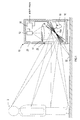
図1に示すように、本実施形態のミリ波撮像装置10は、空港などで乗客が危険物を隠し持っていないかどうかをチェックするのに使用される装置である。ミリ波撮像装置10は、検査対象領域に位置する乗客を被写体2として、被写体2から放射されるミリ波帯の熱雑音を受信することにより被写体2の画像を撮像し、その撮像画像(画像データ)を外部のディスプレイや記憶装置へ出力するよう構成されている。
図1に示すように、本実施形態のミリ波撮像装置10は、空港などで乗客が危険物を隠し持っていないかどうかをチェックするのに使用される装置である。ミリ波撮像装置10は、検査対象領域に位置する乗客を被写体2として、被写体2から放射されるミリ波帯の熱雑音を受信することにより被写体2の画像を撮像し、その撮像画像(画像データ)を外部のディスプレイや記憶装置へ出力するよう構成されている。
すなわち、ミリ波撮像装置10は、ラインセンサ12、レンズ14、および、反射板16を備えている。
ラインセンサ12は、ミリ波帯の熱雑音を受信するための複数の受信素子(図示せず)を直線状に配置することにより構成されている。
ラインセンサ12は、ミリ波帯の熱雑音を受信するための複数の受信素子(図示せず)を直線状に配置することにより構成されている。
レンズ14は、ミリ波帯の熱雑音を集波してラインセンサ12の各受信素子に入射させる。
反射板16は、被写体2から放射されたミリ波帯の熱雑音をレンズ14に向けて反射する。
反射板16は、被写体2から放射されたミリ波帯の熱雑音をレンズ14に向けて反射する。
そして、これら各部は、ミリ波帯の熱雑音を遮蔽可能な材料にて箱状に形成され、下方の側壁の一部が開口されたケース20内に収納されている。
ここで、ラインセンサ12は、受信素子の配列方向が水平方向となり、各受信素子へのミリ波の入射面が下方を向くように、ケース20内の上方に固定されている。また、ラインセンサ12には、各受信素子からの受信信号をそれぞれ増幅する増幅回路や受信信号をそれぞれ検波する検波回路が内蔵されており、各検波回路により検波された検波信号(ミリ波の受信レベルを表す信号)を後述の撮像制御回路30に出力する。
ここで、ラインセンサ12は、受信素子の配列方向が水平方向となり、各受信素子へのミリ波の入射面が下方を向くように、ケース20内の上方に固定されている。また、ラインセンサ12には、各受信素子からの受信信号をそれぞれ増幅する増幅回路や受信信号をそれぞれ検波する検波回路が内蔵されており、各検波回路により検波された検波信号(ミリ波の受信レベルを表す信号)を後述の撮像制御回路30に出力する。
次に、反射板16は、ケース20の側壁に形成された開口部22からケース20内に入射したミリ波を、レンズ14を介してラインセンサ12に導く。反射板16は、ケース20内の下方に、レンズ14を挟んでラインセンサ12と対向するよう配置されている。
また、反射板16は、ラインセンサ12の受信素子の配列方向と平行な回転軸16aを介して、ケース20内の下方に取り付けられており、反射板16の反射面は、回転軸16a周りに回動可能である。
そして、反射板16において、ラインセンサ12と対向する反射面とは反対側の裏面で、且つ、回転軸16aから離れた位置には、反射板16を回転軸16a周りに回動させて、ラインセンサ12に対する反射板16の反射角度を調整するためのアクチュエータ18が設けられている。
このアクチュエータ18は、反射板16の反射角度を、図に示す角度範囲Aで変化させることで、レンズ14を介してラインセンサ12に入射されるミリ波帯の熱雑音の放射位置を、被写体2の頭部から足部にかけて変化させる。つまり、アクチュエータ18は、被写体2を、頭部から足部にかけて垂直方向に走査させる。
また、アクチュエータ18は、反射板16の反射角度を、被写体2の走査領域である角度範囲Aを超えて垂直方向にずらし、図に示す角度Bとする。これによりアクチュエータ18は、ラインセンサ12に対し、ミリ波撮像装置10と被写体2との間の床面から放射されたミリ波帯の熱雑音を入射させることもできる。
なお、図1から明らかなように、本実施形態のアクチュエータ18は、反射板16の裏面にロッドの先端が接続されて、ロッドの突出量を調整することにより反射角度を調整可能なソレノイドにより構成されている。
ただし、アクチュエータ18は、モータを用いて構成してもよい。アクチュエータ18をモータにて構成すれば、モータの回転軸を、複数のロッドを連結したリンク機構を介して、反射板16の裏面に接続するようにすれば、モータの回転により反射板16の反射面を所望角度で変化させることができる。
次に、ケース20内のラインセンサ12近傍には、撮像制御回路30が設けられている。
撮像制御回路30は、制御演算用のマイクロコンピュータ(以下、マイコンという)と、アクチュエータ18を駆動するための駆動回路とを備える。
撮像制御回路30は、制御演算用のマイクロコンピュータ(以下、マイコンという)と、アクチュエータ18を駆動するための駆動回路とを備える。
そして、撮像制御回路30は、予め設定された撮像制御処理をマイコンが実行する。この撮像制御処理では、撮像制御回路30は、アクチュエータ18を駆動することにより被写体2の撮像位置を垂直方向に走査させつつ、所定の走査位置毎に、ラインセンサ12から水平方向一ライン分の検波信号を順次取り込む。続いて、撮像制御回路30は、その取り込んだ水平方向一ライン分の検波信号を垂直方向に並べることで、被写体2の撮像画像を表す画像データを生成し、その画像データを外部のディスプレイや記憶装置へ出力する。
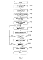
以下、このように被写体2を撮像するために撮像制御回路30にて実行される制御処理を図2に示すフローチャートに沿って説明する。
図2に示す制御処理は、撮像制御回路30に撮像開始指令が入力されてから撮像停止指令が入力されるまでの間、被写体2を撮像するために実行される。この制御処理が開始されると、まずS110(Sはステップを表す)にて、撮像制御回路30に内蔵された駆動回路を介してアクチュエータ18を駆動することにより、反射板16の反射角度を、ミリ波撮像装置10前方の床面から放射されたミリ波帯の熱雑音をラインセンサ12に導く「角度B」に制御する。
図2に示す制御処理は、撮像制御回路30に撮像開始指令が入力されてから撮像停止指令が入力されるまでの間、被写体2を撮像するために実行される。この制御処理が開始されると、まずS110(Sはステップを表す)にて、撮像制御回路30に内蔵された駆動回路を介してアクチュエータ18を駆動することにより、反射板16の反射角度を、ミリ波撮像装置10前方の床面から放射されたミリ波帯の熱雑音をラインセンサ12に導く「角度B」に制御する。
そして、続くS120では、この「角度B」位置にてラインセンサ12から水平方向一ライン分の検波信号を読み込み、続くS130にて、その読み込んだ一ライン分の検波信号の基準値からのずれを、画素毎(換言すれば受信素子毎)に算出する。
つまり、床面から放射されるミリ波帯の熱雑音は略一定であることから、本実施形態では、床面から放射されたミリ波帯の熱雑音を校正用の基準となる熱雑音として、ラインセンサ12を介して検出する。続いて、その検出結果(つまり検波信号)の基準値からのずれを求める。これにより、温度変化等、ミリ波撮像装置10の使用環境変化に伴う検波信号の誤差を算出するのである。
そして、このようにS130にて、検波信号の誤差が算出されると、続くS140にて、その算出された誤差に基づき、今後ラインセンサ12で得られる検波信号を補正するための(換言すれば、検波信号から環境変化に伴う誤差成分を除去するための)補正データを生成し、マイコンのメモリに記憶する。
つまり、本実施形態では、被写体2の撮像を開始する前に、S110~S140の処理を実行することで、ラインセンサ12を介して得られる検波信号(換言すれば画像データ)に対する補正値(補正データ)を求めるのである。
そして、S140にてその補正データが記憶されると、S150に移行し、被写体2の撮像を開始する。
すなわち、S150では、反射板16の反射角度が垂直走査用の角度範囲A内で変化するようにアクチュエータ18を駆動して被写体2を垂直方向に走査するという、被写体2の走査制御(換言すれば、アクチュエータ18の駆動制御)を開始する。
すなわち、S150では、反射板16の反射角度が垂直走査用の角度範囲A内で変化するようにアクチュエータ18を駆動して被写体2を垂直方向に走査するという、被写体2の走査制御(換言すれば、アクチュエータ18の駆動制御)を開始する。
そして、続くS160では、ラインセンサ12から垂直方向1ライン分の検波信号を取り込む。続いてS170にて、その取り込んだ一ライン分の検波信号を、S140で記憶した補正データを用いて画素毎に補正し、その補正後の検波信号を記憶する。続いてS180にて、垂直方向一走査分の検波信号の取り込みが終了したか否かを判断して、垂直方向一走査分の取り込みが終了していなければ、再度S160に移行する。以上のような手順で、垂直方向一走査分の検波信号の取り込み及び補正を実行する。
次に、S180にて、垂直方向一走査分の検波信号の取り込みが終了したと判断されると、S190に移行する。S190では、上記S170の処理で垂直方向の所定の走査位置毎に記憶された全検波信号から2次元画像データを生成し、その生成した画像データを外部装置(上述したディスプレイ等)に出力する。
そして、S190にて画像データの生成・出力を実行すると、続くS200にて、被写体2の撮像を継続するか否か(換言すれば、撮像停止指令が入力されたか否か)を判断する。S200にて、撮像停止指令が入力されておらず、被写体2の撮像を継続すると判断された場合には、再度S160に移行する。一方、S200にて、撮像停止指令が入力されており、被写体2の撮像を継続しないと判断された場合には、S210にて、アクチュエータ18の駆動を停止することで、反射板16による被写体2の走査を停止させ、当該制御処理を終了する。
以上説明したように、本実施形態のミリ波撮像装置10においては、被写体2から放射されたミリ波帯の熱雑音をラインセンサ12に入射させる経路が、ケース20に設けられた開口部22、反射板16、及びレンズ14にて構成されている。これに加え、本実施形態のミリ波撮像装置10では、開口部22と反射板16は、ケース20の下方に配置され、ラインセンサ12は、レンズ14を挟んで、ケース20の上方に配置されている。
このため、本実施形態のミリ波撮像装置10によれば、非特許文献1に記載の装置に比べて重心の位置を低くすることができ、アクチュエータ18により反射板16を回動させた際に装置全体が大きく振動して、装置が倒れやすくなるとか、その振動により被写体2の撮像精度が低下する、といったことを抑制できる。
また、反射板16がミリ波撮像装置10の下方に配置されることから、被写体である人の撮像感度は、上半身よりも足部の方が良くなり、その撮像画像から、足部に隠された物体を良好に検知できるようになる。よって、本実施形態のミリ波撮像装置10によれば、空港等で危険物をチェックするのに極めて有効な装置となり得る。
また、本実施形態では、反射板16をケース20内の下方に配置し、ラインセンサ12をケース20内の上方に配置している。そのため、ラインセンサ12で得られる検波信号(画像データ)を補正するための補正データを生成する際には、反射板16の反射角度を、床面から放射されたミリ波帯の熱雑音がラインセンサ12に入射されるように制御すればよい。
このため、開口部22を電波吸収体で閉塞する等、補正データ生成のための準備をする必要がなく、ミリ波撮像装置10の使い勝手を向上できる。
以上、本発明の一実施形態について説明したが、本発明は上記実施形態に限定されるものではなく、本発明の要旨を逸脱しない範囲内にて種々の態様をとることができる。
以上、本発明の一実施形態について説明したが、本発明は上記実施形態に限定されるものではなく、本発明の要旨を逸脱しない範囲内にて種々の態様をとることができる。
例えば、上記実施形態では、温度等の使用環境変化に伴い撮像画像を補正するための補正データは、ミリ波撮像装置10前方の床面から放射されたミリ波帯の熱雑音をラインセンサ12に入射させることにより算出するものとして説明した。しかし本発明はこれに限定されず、例えば、図1に示すように、補正データ生成用のミリ波帯の熱雑音をラインセンサ12に入射させるための床面には、予め電波吸収体32を埋設しておくようにしてもよい。
そしてこのようにすれば、補正データ生成時にラインセンサ12に入射されるミリ波帯の熱雑音を、より確実に一定にすることができ、補正データの生成精度を向上して、環境変化があっても常時鮮明な撮像画像が得られるようにすることができる。
つまり、本発明の第3の局面においては、ミリ波撮像装置は、画像データに対する補正値を生成するためのミリ波帯の熱雑音をラインセンサ12に入射させる電波吸収体32をさらに備えている構成であってもよい。そして、この電波吸収体32は、例えば図1に示すように、ミリ波撮像装置10と被写体2との間の床面から放射されたミリ波帯の熱雑音をライセンサ12に入射させることができるように、ミリ波撮像装置10前方の床面に埋設されていてもよい。
また、上記実施形態では、ケース20の下方側壁には、単に開口部22が形成されていると説明したが、この開口部22は、被写体2から放射されたミリ波帯の熱雑音(電波)をケース20内の反射板16に導くための開口部であるため、ミリ波帯の電波を透過可能な材料にて閉塞してもよい。そして、このようにすれば、ケース20内に不要なもの(ゴミや埃等)が侵入するのを抑制できる。
Claims (3)
- 直線状に配置された、ミリ波帯の熱雑音を受信するための複数の受信素子を有するラインセンサと、
ミリ波帯の熱雑音を前記複数の受信素子の各々に入射させるためのレンズと、
被写体から放射されたミリ波帯の熱雑音を前記レンズに向けて反射する反射板と、
前記反射板を前記ラインセンサに対して水平方向に配置された回転軸周りに回動させることで、前記被写体を前記ラインセンサに対して垂直方向に走査し、各走査位置にて前記被写体から放射された水平方向一ライン分のミリ波帯の熱雑音を、前記反射板及び前記レンズを介して前記複数の受信素子の各々に入射させる駆動手段と、
前記駆動手段を介して前記反射板を前記回動軸周りに回動させると共に、その回動に同期した複数の走査位置毎に前記複数の受信素子の各々から出力される受信信号を取り込むことで、前記被写体のミリ波画像を表す画像データを生成する制御手段と、
ミリ波帯の熱雑音を遮蔽可能な材料にて箱状に形成され、前記各部を収納するためのケースと、
を備え、前記ケース内では、前記ラインセンサが、前記複数の受信素子の配列方向が前記回転軸と略平行な水平方向となるよう、前記レンズを挟んで前記反射板の上方に配置され、
前記ケースの下方側壁には、前記被写体から放射されたミリ波帯の熱雑音を前記反射板に導く開口部が形成されていることを特徴とするミリ波撮像装置。 - 前記反射板は、前記回転軸周りに回動されることにより、所定の回動基準位置にて、前記ケースの前記開口部よりも外側に位置する床面から入射されたミリ波帯の熱雑音を前記レンズに向けて反射するよう構成されており、
前記制御手段は、前記反射板を前記回動軸周りに回動させて前記被写体の画像データの生成を開始する前に、前記反射板を前記回動基準位置に制御することにより、前記床面から入射されたミリ波帯の熱雑音に対応した受信信号を前記ラインセンサから取り込み、該受信信号に基づき、前記画像データに対する補正値を生成することを特徴とする請求項1に記載のミリ波撮像装置。 - 前記画像データに対する補正値を生成するためのミリ波帯の熱雑音を前記ラインセンサに入射させる電波吸収体をさらに備えていることを特徴とする請求項1または2に記載のミリ波撮像装置。
Applications Claiming Priority (2)
| Application Number | Priority Date | Filing Date | Title |
|---|---|---|---|
| JP2010-162059 | 2010-07-16 | ||
| JP2010162059A JP5626723B2 (ja) | 2010-07-16 | 2010-07-16 | ミリ波撮像装置 |
Publications (1)
| Publication Number | Publication Date |
|---|---|
| WO2012008583A1 true WO2012008583A1 (ja) | 2012-01-19 |
Family
ID=45469577
Family Applications (1)
| Application Number | Title | Priority Date | Filing Date |
|---|---|---|---|
| PCT/JP2011/066249 Ceased WO2012008583A1 (ja) | 2010-07-16 | 2011-07-15 | ミリ波撮像装置 |
Country Status (2)
| Country | Link |
|---|---|
| JP (1) | JP5626723B2 (ja) |
| WO (1) | WO2012008583A1 (ja) |
Cited By (6)
| Publication number | Priority date | Publication date | Assignee | Title |
|---|---|---|---|---|
| CN106154345A (zh) * | 2015-03-27 | 2016-11-23 | 常州吉赫射频电子技术有限公司 | 椭球面被动毫米波成像系统 |
| CN109444978A (zh) * | 2018-12-29 | 2019-03-08 | 清华大学 | 毫米波/太赫兹波成像设备及对人体或物品的检测方法 |
| CN109828313A (zh) * | 2018-12-29 | 2019-05-31 | 清华大学 | 毫米波/太赫兹波成像设备及对人体或物品的检测方法 |
| CN109870738A (zh) * | 2018-12-29 | 2019-06-11 | 清华大学 | 毫米波/太赫兹波成像设备及其校正方法 |
| WO2020134326A1 (zh) * | 2018-12-29 | 2020-07-02 | 清华大学 | 毫米波/太赫兹波成像设备、检测方法以及校正方法 |
| CN119644445A (zh) * | 2024-12-31 | 2025-03-18 | 北京神目科技有限公司 | 毫米波成像设备、安检设备以及安检方法 |
Families Citing this family (8)
| Publication number | Priority date | Publication date | Assignee | Title |
|---|---|---|---|---|
| JP2013167529A (ja) * | 2012-02-15 | 2013-08-29 | Maspro Denkoh Corp | 電波撮像装置 |
| JP2013246138A (ja) * | 2012-05-29 | 2013-12-09 | Maspro Denkoh Corp | 携帯型マイクロ波測定装置 |
| JP6276736B2 (ja) * | 2015-08-20 | 2018-02-07 | 海洋総合開発株式会社 | 物質識別装置 |
| JP2020204513A (ja) * | 2019-06-17 | 2020-12-24 | 株式会社東芝 | システム及び検査方法 |
| CN110568512A (zh) * | 2019-10-23 | 2019-12-13 | 中国工程物理研究院电子工程研究所 | 一种毫米波人体安检门 |
| JP7605687B2 (ja) * | 2021-05-10 | 2024-12-24 | 日本信号株式会社 | 所持物検査装置 |
| JP7733996B2 (ja) * | 2021-06-07 | 2025-09-04 | 日本信号株式会社 | イメージング装置 |
| JP2023163646A (ja) * | 2022-04-28 | 2023-11-10 | 日本信号株式会社 | パッシブイメージング装置 |
Citations (1)
| Publication number | Priority date | Publication date | Assignee | Title |
|---|---|---|---|---|
| WO2008117674A1 (ja) * | 2007-03-26 | 2008-10-02 | Masprodenkoh Kabushikikaisha | ミリ波撮像装置及び撮像画像表示装置 |
-
2010
- 2010-07-16 JP JP2010162059A patent/JP5626723B2/ja not_active Expired - Fee Related
-
2011
- 2011-07-15 WO PCT/JP2011/066249 patent/WO2012008583A1/ja not_active Ceased
Patent Citations (1)
| Publication number | Priority date | Publication date | Assignee | Title |
|---|---|---|---|---|
| WO2008117674A1 (ja) * | 2007-03-26 | 2008-10-02 | Masprodenkoh Kabushikikaisha | ミリ波撮像装置及び撮像画像表示装置 |
Non-Patent Citations (2)
| Title |
|---|
| JUN NAKATA ET AL.: "Real-time Calibration Method of MM-wave Image Using Upper-edge of Back-ground Temperature", 2009 NEN IEICE ELECTRONICS SOCIETY TAIKAI KOEN RONBUNSHU 1, 1 September 2009 (2009-09-01), pages 143, XP008148093 * |
| YASUHIRO SATO ET AL.: "Passive Millimeter Wave Imaging Technology for Security Systems", JOURNAL OF THE SOCIETY OF INSTRUMENT AND CONTROL ENGINEERS, vol. 48, no. 10, 10 October 2009 (2009-10-10), pages 748 - 753 * |
Cited By (9)
| Publication number | Priority date | Publication date | Assignee | Title |
|---|---|---|---|---|
| CN106154345A (zh) * | 2015-03-27 | 2016-11-23 | 常州吉赫射频电子技术有限公司 | 椭球面被动毫米波成像系统 |
| CN109444978A (zh) * | 2018-12-29 | 2019-03-08 | 清华大学 | 毫米波/太赫兹波成像设备及对人体或物品的检测方法 |
| CN109828313A (zh) * | 2018-12-29 | 2019-05-31 | 清华大学 | 毫米波/太赫兹波成像设备及对人体或物品的检测方法 |
| CN109870738A (zh) * | 2018-12-29 | 2019-06-11 | 清华大学 | 毫米波/太赫兹波成像设备及其校正方法 |
| WO2020134326A1 (zh) * | 2018-12-29 | 2020-07-02 | 清华大学 | 毫米波/太赫兹波成像设备、检测方法以及校正方法 |
| EP3904916A4 (en) * | 2018-12-29 | 2022-12-28 | Tsinghua University | MILLIMETER WAVE/TERAHERTWAVE IMAGING DEVICE, VERIFICATION PROCEDURE AND CALIBRATION PROCEDURE |
| CN109828313B (zh) * | 2018-12-29 | 2023-11-24 | 清华大学 | 毫米波/太赫兹波成像设备及对人体或物品的检测方法 |
| CN109444978B (zh) * | 2018-12-29 | 2024-02-02 | 清华大学 | 毫米波/太赫兹波成像设备及对人体或物品的检测方法 |
| CN119644445A (zh) * | 2024-12-31 | 2025-03-18 | 北京神目科技有限公司 | 毫米波成像设备、安检设备以及安检方法 |
Also Published As
| Publication number | Publication date |
|---|---|
| JP5626723B2 (ja) | 2014-11-19 |
| JP2012021954A (ja) | 2012-02-02 |
Similar Documents
| Publication | Publication Date | Title |
|---|---|---|
| JP5626723B2 (ja) | ミリ波撮像装置 | |
| US7193695B2 (en) | Survey system | |
| US11733357B2 (en) | 3-dimensional measuring device | |
| WO2019163673A1 (ja) | 光測距装置 | |
| US11408982B2 (en) | Electromagnetic wave detection apparatus, program, and electromagnetic wave detection system | |
| JP6010505B2 (ja) | 画像取得装置及び画像取得装置のフォーカス方法 | |
| US11573301B2 (en) | Electromagnetic wave detection apparatus, program, and electromagnetic wave detection system | |
| JP7034485B2 (ja) | 電磁波測定装置 | |
| CN115754981B (zh) | 基于振镜的激光控制方法、标定方法、装置和激光雷达 | |
| EP3904916B1 (en) | Millimeter wave/terahertz wave imaging apparatus, and detection method thereof | |
| US20200033116A1 (en) | Electromagnetic wave detection apparatus, program, and electromagnetic wave detection system | |
| JP5464644B2 (ja) | ミリ波撮像装置およびプログラム | |
| US20170035300A1 (en) | Object information acquiring apparatus and control method for the object information acquiring apparatus | |
| JP2011237417A (ja) | ミリ波撮像装置 | |
| KR20100106010A (ko) | 변위센서를 이용한 휴대폰 카메라의 틸트 및 성능 측정시스템 | |
| US20200018858A1 (en) | Electromagnetic wave detection apparatus, program, and electromagnetic wave detection system | |
| JP2011127914A (ja) | ミリ波撮像装置、ミリ波撮像システムおよびプログラム | |
| CN115201230B (zh) | 基于透射成像的检测装置和检测方法 | |
| US20230133411A1 (en) | Detection device, correction device, processing device, and article manufacturing method | |
| US11131543B2 (en) | Three-dimensional measuring apparatus and robot system | |
| JP6423032B2 (ja) | 3次元測量装置 | |
| JP2013167529A (ja) | 電波撮像装置 | |
| JP2011242229A (ja) | イメージング装置およびイメージング方法 | |
| CN120403462B (zh) | 一种光声检测系统及激光光斑校准方法 | |
| JP2014145684A (ja) | 測定装置 |
Legal Events
| Date | Code | Title | Description |
|---|---|---|---|
| 121 | Ep: the epo has been informed by wipo that ep was designated in this application |
Ref document number: 11806913 Country of ref document: EP Kind code of ref document: A1 |
|
| NENP | Non-entry into the national phase |
Ref country code: DE |
|
| 122 | Ep: pct application non-entry in european phase |
Ref document number: 11806913 Country of ref document: EP Kind code of ref document: A1 |