WO2012008205A1 - 電子機器および表示装置 - Google Patents
電子機器および表示装置 Download PDFInfo
- Publication number
- WO2012008205A1 WO2012008205A1 PCT/JP2011/060388 JP2011060388W WO2012008205A1 WO 2012008205 A1 WO2012008205 A1 WO 2012008205A1 JP 2011060388 W JP2011060388 W JP 2011060388W WO 2012008205 A1 WO2012008205 A1 WO 2012008205A1
- Authority
- WO
- WIPO (PCT)
- Prior art keywords
- substrate
- metal plate
- chassis
- contact
- protrusion
- Prior art date
- Legal status (The legal status is an assumption and is not a legal conclusion. Google has not performed a legal analysis and makes no representation as to the accuracy of the status listed.)
- Ceased
Links
Images



















Classifications
-
- H—ELECTRICITY
- H05—ELECTRIC TECHNIQUES NOT OTHERWISE PROVIDED FOR
- H05K—PRINTED CIRCUITS; CASINGS OR CONSTRUCTIONAL DETAILS OF ELECTRIC APPARATUS; MANUFACTURE OF ASSEMBLAGES OF ELECTRICAL COMPONENTS
- H05K7/00—Constructional details common to different types of electric apparatus
- H05K7/20—Modifications to facilitate cooling, ventilating, or heating
- H05K7/2039—Modifications to facilitate cooling, ventilating, or heating characterised by the heat transfer by conduction from the heat generating element to a dissipating body
-
- G—PHYSICS
- G02—OPTICS
- G02F—OPTICAL DEVICES OR ARRANGEMENTS FOR THE CONTROL OF LIGHT BY MODIFICATION OF THE OPTICAL PROPERTIES OF THE MEDIA OF THE ELEMENTS INVOLVED THEREIN; NON-LINEAR OPTICS; FREQUENCY-CHANGING OF LIGHT; OPTICAL LOGIC ELEMENTS; OPTICAL ANALOGUE/DIGITAL CONVERTERS
- G02F1/00—Devices or arrangements for the control of the intensity, colour, phase, polarisation or direction of light arriving from an independent light source, e.g. switching, gating or modulating; Non-linear optics
- G02F1/01—Devices or arrangements for the control of the intensity, colour, phase, polarisation or direction of light arriving from an independent light source, e.g. switching, gating or modulating; Non-linear optics for the control of the intensity, phase, polarisation or colour
- G02F1/13—Devices or arrangements for the control of the intensity, colour, phase, polarisation or direction of light arriving from an independent light source, e.g. switching, gating or modulating; Non-linear optics for the control of the intensity, phase, polarisation or colour based on liquid crystals, e.g. single liquid crystal display cells
- G02F1/133—Constructional arrangements; Operation of liquid crystal cells; Circuit arrangements
- G02F1/1333—Constructional arrangements; Manufacturing methods
- G02F1/133382—Heating or cooling of liquid crystal cells other than for activation, e.g. circuits or arrangements for temperature control, stabilisation or uniform distribution over the cell
- G02F1/133385—Heating or cooling of liquid crystal cells other than for activation, e.g. circuits or arrangements for temperature control, stabilisation or uniform distribution over the cell with cooling means, e.g. fans
-
- G—PHYSICS
- G02—OPTICS
- G02F—OPTICAL DEVICES OR ARRANGEMENTS FOR THE CONTROL OF LIGHT BY MODIFICATION OF THE OPTICAL PROPERTIES OF THE MEDIA OF THE ELEMENTS INVOLVED THEREIN; NON-LINEAR OPTICS; FREQUENCY-CHANGING OF LIGHT; OPTICAL LOGIC ELEMENTS; OPTICAL ANALOGUE/DIGITAL CONVERTERS
- G02F1/00—Devices or arrangements for the control of the intensity, colour, phase, polarisation or direction of light arriving from an independent light source, e.g. switching, gating or modulating; Non-linear optics
- G02F1/01—Devices or arrangements for the control of the intensity, colour, phase, polarisation or direction of light arriving from an independent light source, e.g. switching, gating or modulating; Non-linear optics for the control of the intensity, phase, polarisation or colour
- G02F1/13—Devices or arrangements for the control of the intensity, colour, phase, polarisation or direction of light arriving from an independent light source, e.g. switching, gating or modulating; Non-linear optics for the control of the intensity, phase, polarisation or colour based on liquid crystals, e.g. single liquid crystal display cells
- G02F1/133—Constructional arrangements; Operation of liquid crystal cells; Circuit arrangements
- G02F1/1333—Constructional arrangements; Manufacturing methods
- G02F1/1345—Conductors connecting electrodes to cell terminals
- G02F1/13452—Conductors connecting driver circuitry and terminals of panels
-
- H—ELECTRICITY
- H05—ELECTRIC TECHNIQUES NOT OTHERWISE PROVIDED FOR
- H05K—PRINTED CIRCUITS; CASINGS OR CONSTRUCTIONAL DETAILS OF ELECTRIC APPARATUS; MANUFACTURE OF ASSEMBLAGES OF ELECTRICAL COMPONENTS
- H05K7/00—Constructional details common to different types of electric apparatus
- H05K7/20—Modifications to facilitate cooling, ventilating, or heating
- H05K7/20954—Modifications to facilitate cooling, ventilating, or heating for display panels
- H05K7/20963—Heat transfer by conduction from internal heat source to heat radiating structure
-
- H—ELECTRICITY
- H10—SEMICONDUCTOR DEVICES; ELECTRIC SOLID-STATE DEVICES NOT OTHERWISE PROVIDED FOR
- H10W—GENERIC PACKAGES, INTERCONNECTIONS, CONNECTORS OR OTHER CONSTRUCTIONAL DETAILS OF DEVICES COVERED BY CLASS H10
- H10W40/00—Arrangements for thermal protection or thermal control
- H10W40/10—Arrangements for heating
-
- H—ELECTRICITY
- H10—SEMICONDUCTOR DEVICES; ELECTRIC SOLID-STATE DEVICES NOT OTHERWISE PROVIDED FOR
- H10W—GENERIC PACKAGES, INTERCONNECTIONS, CONNECTORS OR OTHER CONSTRUCTIONAL DETAILS OF DEVICES COVERED BY CLASS H10
- H10W40/00—Arrangements for thermal protection or thermal control
- H10W40/60—Securing means for detachable heating or cooling arrangements, e.g. clamps
- H10W40/611—Bolts or screws
-
- G—PHYSICS
- G02—OPTICS
- G02F—OPTICAL DEVICES OR ARRANGEMENTS FOR THE CONTROL OF LIGHT BY MODIFICATION OF THE OPTICAL PROPERTIES OF THE MEDIA OF THE ELEMENTS INVOLVED THEREIN; NON-LINEAR OPTICS; FREQUENCY-CHANGING OF LIGHT; OPTICAL LOGIC ELEMENTS; OPTICAL ANALOGUE/DIGITAL CONVERTERS
- G02F1/00—Devices or arrangements for the control of the intensity, colour, phase, polarisation or direction of light arriving from an independent light source, e.g. switching, gating or modulating; Non-linear optics
- G02F1/01—Devices or arrangements for the control of the intensity, colour, phase, polarisation or direction of light arriving from an independent light source, e.g. switching, gating or modulating; Non-linear optics for the control of the intensity, phase, polarisation or colour
- G02F1/13—Devices or arrangements for the control of the intensity, colour, phase, polarisation or direction of light arriving from an independent light source, e.g. switching, gating or modulating; Non-linear optics for the control of the intensity, phase, polarisation or colour based on liquid crystals, e.g. single liquid crystal display cells
- G02F1/133—Constructional arrangements; Operation of liquid crystal cells; Circuit arrangements
- G02F1/1333—Constructional arrangements; Manufacturing methods
- G02F1/133308—Support structures for LCD panels, e.g. frames or bezels
- G02F1/133314—Back frames
Definitions
- the present invention relates to an electronic device and a display device, and particularly to an electronic device and a display device including a substrate on which a semiconductor package is attached.
- FIG. 40 is a cross-sectional view showing the structure of an electronic apparatus according to a conventional example including a substrate to which a semiconductor package is attached.
- an electronic apparatus 5001 includes a plurality of semiconductor packages 5002, a substrate 5003 to which a plurality of semiconductor packages 5002 are attached, a heat dissipation sheet 5004 disposed on the semiconductor package 5002, and heat dissipation.
- a metal plate 5005 that is in contact with the semiconductor package 5002 via the sheet 5004 and a chassis 5006 that is disposed at a predetermined distance from the substrate 5003 are provided.
- the plurality of semiconductor packages 5002 include semiconductor packages 5002a and 5002b having different thicknesses.
- the semiconductor package 5002b has a larger thickness than the semiconductor package 5002a.
- the plurality of heat radiation sheets 5004 include a heat radiation sheet 5004a disposed on the semiconductor package 5002a and a heat radiation sheet 5004b disposed on the semiconductor package 5002b.
- the heat dissipation sheet 5004b has a smaller thickness than the heat dissipation sheet 5004a.
- the semiconductor package 5002a is in contact with the metal plate 5005 through the heat dissipation sheet 5004a, and the semiconductor package 5002b is in contact with the metal plate 5005 through the heat dissipation sheet 5004b. Thereby, the heat generated in the semiconductor package 5002 can be radiated to the metal plate 5005.
- the substrate 5003 and the metal plate 5005 are fixed to the chassis 5006 using a fixing member (not shown).
- the metal plate 5005 may not contact the semiconductor package 5002 (heat dissipation sheet 5004) due to manufacturing variations.
- the mounting height of the semiconductor package 5002a (distance from the mounting surface of the substrate 5003 to the upper surface of the semiconductor package 5002a) becomes smaller than the design value due to manufacturing variations, the metal plate 5005 In some cases, the semiconductor package 5002a (heat dissipating sheet 5004a) may not come into contact. For this reason, it is difficult to dissipate heat generated in the semiconductor package 5002a to the metal plate 5005.
- the present invention has been made to solve the above-described problems, and an object of the present invention is to provide an electronic apparatus and a display device that can suppress a decrease in heat dissipation. .
- an electronic apparatus is disposed to face a semiconductor package, a substrate having a mounting surface to which the semiconductor package is mounted, and a surface opposite to the mounting surface of the substrate. And a first metal plate provided with a first protrusion that protrudes toward the substrate, and a first heat conducting member disposed between the first protrusion of the first metal plate and the substrate.
- the mounting height of the semiconductor package (the distance from the mounting surface of the substrate to the outer surface (for example, the upper surface) of the semiconductor package) becomes smaller than the design value due to manufacturing variations.
- the first protrusion can be prevented from coming into contact with the substrate (first heat conducting member). Thereby, it can suppress that the heat dissipation of an electronic device falls.
- the first metal plate can be provided with the first protruding portion that protrudes toward the substrate, whereby the thickness of the first heat conducting member can be reduced.
- the heat generated in the semiconductor package can be radiated to the back surface (surface opposite to the mounting surface) side of the substrate, so that the heat generated in the semiconductor package is transferred to the substrate.
- the heat generated in the semiconductor package is transferred to the substrate.
- the first protrusion includes a contact portion that is in contact with the substrate via the first heat conducting member, and a spring portion that biases the contact portion toward the substrate. . If comprised in this way, since a contact part can be urged
- the first projecting portion includes the contact portion and the spring portion
- the first projecting portion is preferably formed by bending the first metal plate. If comprised in this way, while the 1st protrusion part which protrudes in a board
- a cutout portion is preferably formed around the first protruding portion of the first metal plate. If comprised in this way, a 1st protrusion part can be easily formed by bending a 1st metal plate. Moreover, a 1st protrusion part can be formed in the desired position of a 1st metal plate.
- the first metal plate straddles the cutout portion, and the first protrusion and the first metal plate.
- the 2nd heat conductive member contacted with parts other than the 1st protrusion part of this is provided.
- heat from the semiconductor package (first heat conducting member) is transmitted (heat radiation) in a direction in which the cutout is not formed.
- a semiconductor package (first heat conducting member) by providing a second heat conducting member that straddles the cutout portion and is in contact with a portion other than the first projecting portion and the first projecting portion of the first metal plate. Can be transmitted (radiated) in the direction in which the cutout portion is not formed and the direction in which the cutout portion is formed (the direction in which the second heat conducting member is provided). Thereby, the heat dissipation of an electronic device can be improved.
- the electronic device preferably further includes a second metal plate disposed on the mounting surface side of the substrate, and a third heat conducting member disposed between the second metal plate and the semiconductor package. . If comprised in this way, the heat
- the second metal plate functions to press the substrate toward the first metal plate through the third heat conducting member and the semiconductor package.
- a 1st protrusion part (1st metal plate) does not contact a 1st heat conductive member. Can be suppressed. Thereby, it can suppress more that the heat dissipation of an electronic device falls.
- the second metal plate preferably includes a second projecting portion that projects toward the semiconductor package and contacts the third heat conducting member. According to this configuration, for example, even when a plurality of semiconductor packages having different thicknesses are attached to the substrate, the protrusion height of each of the plurality of second protrusions is set to By setting according to the thickness, all the semiconductor packages can be easily brought into contact with the second metal plate (second projecting portion).
- the thickness of the third heat conducting member can be reduced by providing the second metal plate with the second projecting portion projecting to the semiconductor package side.
- a plurality of semiconductor packages and first heat conductive members are provided, and at least two first heat conductive members of the plurality of first heat conductive members are provided. Are formed to have the same thickness and are in contact with one first protrusion. As described above, whether or not the plurality of semiconductor packages have different thicknesses in the electronic device according to the first aspect, even when a plurality of semiconductor packages and a plurality of first heat conducting members are provided, respectively. Regardless, at least two first heat conductive members of the plurality of first heat conductive members can be formed to have the same thickness and contact one first protrusion.
- the first metal plate is provided with heat radiation fins. If comprised in this way, the heat dissipation of an electronic device can be improved more.
- the radiating fin is preferably formed by cutting out the first metal plate. If comprised in this way, a radiation fin can be easily formed in a 1st metal plate.
- the first projecting portion includes a contact portion that is in contact with the substrate via the first heat conducting member, and a through hole is formed in the contact portion. If comprised in this way, when attaching a board
- the electronic apparatus preferably further includes at least one of a screw and a band that are attached to the substrate and the first metal plate and press the central portion of the substrate toward the first metal plate. If comprised in this way, a 1st protrusion part can be made to contact a board
- the electronic apparatus preferably further includes a first adhesive layer that adheres the substrate and the first metal plate. If comprised in this way, since it can suppress that a 1st metal plate leaves
- a third protrusion that protrudes toward the substrate is provided at a position corresponding to the edge of the substrate on the first metal plate, and the edge of the substrate is The first metal plate is attached to the third protrusion. If comprised in this way, a clearance gap can be formed between the center part of a board
- the first metal for adjusting the distance from the first metal plate to the substrate is between the third protrusion and the substrate.
- An elastic body is provided. If comprised in this way, since the distance from a 1st protrusion part to a board
- the first protrusion is attached to the first metal plate via a second elastic body for adjusting a distance from the first protrusion to the first metal plate. It has been. If comprised in this way, since the distance from a 1st protrusion part to a 1st metal plate can be adjusted, the distance from a 1st protrusion part to a board
- a second adhesive layer is disposed between the first heat conducting member and the first protrusion. If comprised in this way, since a contact with the 1st heat conductive member and the 1st projection part can be maintained satisfactorily, it will make it easy to transmit the heat which generates in a semiconductor package to the 1st projection part (heat dissipation) more. be able to. Thereby, the heat dissipation of an electronic device can be improved more.
- a display device includes the electronic device having the above-described configuration. If comprised in this way, the display apparatus which can suppress that heat dissipation falls will be obtained.
- FIG. 1 is a cross-sectional view illustrating a structure of a liquid crystal display device according to a first embodiment of the present invention. It is sectional drawing which showed the structure of the board
- FIG. 6 is a cross-sectional view showing a structure around a substrate of a liquid crystal display device according to a second embodiment of the present invention.
- FIG. 5 is a plan view for explaining the structure of the chassis shown in FIG. 4.
- FIG. 5 is a cross-sectional view for explaining the structure of the chassis shown in FIG. 4.
- FIG. 5 is a plan view for explaining the structure of the chassis shown in FIG. 4.
- FIG. 6 is a cross-sectional view illustrating a structure around a substrate of a liquid crystal display device according to a fourth embodiment of the present invention.
- FIG. 6 is a cross-sectional view illustrating a structure around a substrate of a liquid crystal display device according to a fifth embodiment of the present invention. It is sectional drawing which showed the structure around the board
- FIG. 16 is an enlarged sectional view for explaining a structure around the substrate shown in FIG. 15. It is sectional drawing which showed the structure of the board
- FIG. 20 is an enlarged cross-sectional view for explaining the structure around the substrate shown in FIG. 19.
- the liquid crystal display device 1 constitutes, for example, a liquid crystal television receiver (not shown).
- the liquid crystal display device 1 includes a liquid crystal display panel 2, an optical sheet 3 and a plurality of light sources 4 arranged on the back surface (back surface) side of the liquid crystal display panel 2, and A sheet metal chassis 5 that houses the light source 4, a plurality of semiconductor packages 6 disposed outside the chassis 5, a substrate 7 to which the plurality of semiconductor packages 6 are attached and disposed opposite to the chassis 5, the chassis 5, and It is comprised by the heat radiating sheet (heat conductive sheet) 8 arrange
- the optical sheet 3, the plurality of light sources 4, the chassis 5, and the like constitute a direct type backlight device.
- the liquid crystal display device 1 is an example of the “electronic device” and “display device” in the present invention
- the chassis 5 is an example of the “first metal plate” in the present invention.
- the heat radiation sheet 8 (8a, 8b) is an example of the “first heat conducting member” in the present invention.
- the liquid crystal display panel 2 includes two glass substrates that sandwich a liquid crystal layer (not shown).
- the liquid crystal display panel 2 functions as a display panel when illuminated by the light source 4.
- the optical sheet 3 is composed of a plurality of sheets such as a prism sheet and a lens sheet, for example.
- the light source 4 is formed by, for example, a fluorescent lamp.
- the light source 4 may be formed of, for example, an LED (Light Emitting Diode) other than the fluorescent lamp.
- a reflection sheet (not shown) may be disposed on the back side of the light source 4.
- the chassis 5 is formed with a plurality of ribs 10 protruding toward the substrate 7 (outside).
- the plurality of ribs 10 are formed by, for example, drawing.
- the plurality of ribs 10 include ribs 11 and 12 that are in contact with the semiconductor package 6 via the heat dissipation sheet 8 and a plurality of ribs 13.
- the ribs 11 and 12 are an example of the “first protrusion” in the present invention
- the rib 13 is an example of the “third protrusion” in the present invention.
- Ribs 11 and 12 are formed to have the same protruding height (height in the thickness direction).
- the rib 11 is formed at a position corresponding to a semiconductor package 6a described later (a position facing an element mounting portion 7a (see FIG. 3) described later) of the substrate 7, and the rib 12 is formed by a semiconductor package 6b described later. (A position facing an element mounting portion 7b (see FIG. 3) described later) of the substrate 7.
- the ribs 11 and 12 are formed with contact portions 11a and 12a that are in contact with the substrate 7 through the heat dissipation sheet 8, respectively.
- the contact portions 11a and 12a are formed flat, for example.
- the plurality of ribs 13 are arranged at positions (positions directly above the edge 7d) corresponding to the edge 7d (see FIG. 3) described later of the substrate 7 of the chassis 5.
- the plurality of ribs 13 are formed so as to have the same protruding height. Further, the plurality of ribs 13 have a protruding height larger than that of the ribs 11 and 12. Further, the protruding height of the plurality of ribs 13 is set to the same size as the combined value of the protruding height of the rib 11 (or rib 12) and the thickness of the heat radiating sheet 8a (or heat radiating sheet 8b) described later. Has been.
- the plurality of semiconductor packages 6 are elements for performing processing such as FRC (Frame Rate Control), for example, and generate a large amount of heat during operation.
- the plurality of semiconductor packages 6 include semiconductor packages 6a and 6b having different thicknesses.
- the semiconductor package 6b has a larger thickness than the semiconductor package 6a.
- the plurality of semiconductor packages 6a and 6b are attached to the attachment surface of the substrate 7 using a solder layer (not shown).
- the mounting height of the semiconductor package 6b (distance from the mounting surface of the substrate 7 to the outer surface of the semiconductor package 6b (the lower surface in FIG. 2)) H2 is the mounting height of the semiconductor package 6a (the mounting surface of the substrate 7). Distance from the outer surface of the semiconductor package 6a (the lower surface in FIG. 2) H1.
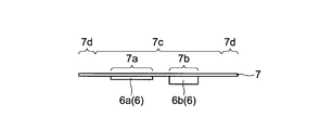
- the substrate 7 includes a central portion 7c including element mounting portions 7a and 7b to which a plurality of semiconductor packages 6a and 6b are respectively attached, and an edge portion 7d (a portion other than the central portion 7c).
- the heat generated in the semiconductor packages 6a and 6b is transmitted to the substrate 7 through a solder layer (not shown).
- the element mounting portions 7 a and 7 b of the substrate 7 may be provided with through holes (not shown) filled with a metal material in order to conduct heat in the thickness direction of the substrate 7.
- the back surface (the surface opposite to the mounting surface) of the edge portion 7d of the substrate 7 is fixed to the rib 13 of the chassis 5 using a screw or the like (not shown).
- the heat radiation sheet 8 is formed of a sheet member having a high thermal conductivity. Moreover, the heat radiating sheet 8 is formed to be elastically deformable so as to be compressed by being pressed. Specifically, the heat radiating sheet 8 is formed of silicone rubber, acrylic rubber, or the like, and the Asker C hardness of the heat radiating sheet 8 is, for example, about 10 to 60.
- the plurality of heat dissipation sheets 8 include a heat dissipation sheet 8 a disposed on the back surface of the element mounting portion 7 a of the substrate 7 and a heat dissipation sheet 8 b disposed on the back surface of the element mounting portion 7 b of the substrate 7. .
- the element mounting portion 7a of the substrate 7 is in contact with the contact portion 11a of the rib 11 via the heat dissipation sheet 8a, and the element mounting portion 7b of the substrate 7 is contacted with the contact portion 12a of the rib 12 via the heat dissipation sheet 8b. Is touching.
- the heat generated in the semiconductor package 6 is transferred to the substrate 7 and the heat dissipation sheet 8 ( Heat can be radiated to the chassis 5 via 8a and 8b).
- the distance from the ribs 11 and 12 to the substrate 7 is the same. Therefore, the ribs 11 and 12 can be prevented from coming into contact with the substrate 7 (heat dissipating sheet 8). Thereby, it can suppress that the heat dissipation of the liquid crystal display device 1 falls.
- the ribs 11 and 12 projecting toward the substrate 7 are provided on the chassis 5 to reduce the thickness of the heat radiation sheet 8 (8a and 8b). Thereby, while being able to improve the heat dissipation of the liquid crystal display device 1, the cost of the thermal radiation sheet 8 (8a and 8b) can be reduced.
- the heat generated in the semiconductor package 6 can be radiated to the back surface (surface opposite to the mounting surface) side of the substrate 7, so that the heat generated in the semiconductor package 6 is dissipated.
- a heat radiating member or the like may not be provided on the mounting surface side of the substrate 7. Thereby, it is also possible to suppress an increase in the size of the entire liquid crystal display device 1.
- the ribs 13 projecting toward the board 7 are provided at positions corresponding to the edges 7 d of the board 7 of the chassis 5, and the edges 7 d of the board 7 are connected to the ribs of the chassis 5. Attach to 13. Thereby, a gap can be formed between the central portion 7 c of the substrate 7 and the chassis 5.
- the semiconductor package 6 since the semiconductor package 6 generates a large amount of heat, it is particularly effective to configure the liquid crystal display device 1 as described above.
- the spring portions 111b and 112b are provided to bring the substrate 7 (heat radiation sheet 8) into contact with the contact portions 111a and 112a. The case where it is provided will be described.
- the chassis 105 includes a plurality of protrusions 111 and 112 that protrude toward the substrate 7 (outside), a plurality of ribs 13, and a plurality of fins that function as heat dissipation fins. Portions 113 and 114 are formed.
- the chassis 105 is an example of the “first metal plate” in the present invention, and the protrusions 111 and 112 are examples of the “first protrusion” and the “radiating fin” in the present invention.
- the fin portions 113 and 114 are an example of the “radiating fins” in the present invention.
- the plurality of protrusions 111 and 112 are brought into contact with the substrate 7 through the heat dissipation sheet 8.
- the plurality of protrusions 111 and 112 are formed to have the same protrusion height.
- the protruding portion 111 is formed at a position corresponding to the semiconductor package 6a (a position facing the element mounting portion 7a of the substrate 7), and the protruding portion 112 is positioned corresponding to the semiconductor package 6b (an element of the substrate 7). (Position facing the mounting portion 7b).
- the protrusion part 111 contains the contact part 111a contacted with the semiconductor package 6 (heat dissipation sheet 8), and the spring part 111b which urges
- the spring portion 111b connects the contact portion 111a and the flat portion 105a of the chassis 105 (a portion of the chassis 105 other than the protruding portions 111 and 112, the ribs 13, and the fin portions 113 and 114).
- the projecting portion 112 includes a contact portion 112a that comes into contact with the semiconductor package 6 (heat radiation sheet 8) and a spring portion 112b that biases the contact portion 112a toward the substrate 7 side.
- the spring portion 112 b connects the contact portion 112 a and the flat portion 105 a of the chassis 105.
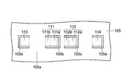
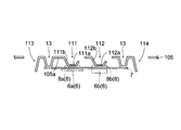
- the protrusions 111 and 112 are formed by cutting out and bending a part of the chassis 105. Specifically, as shown in FIG. 5, for example, U-shaped cutout portions 105 b and 105 c are formed around the protrusions 111 and 112, respectively. And the protrusion parts 111 and 112 are formed by bending in the position of the broken line of FIG.
- the contact part 111a of the protrusion part 111 will arrange
- the spring portion 111b of the protruding portion 111 is elastically deformed, so that the contact pressure of the contact portion 111a with respect to the heat radiation sheet 8a (substrate 7) is suppressed from being excessively increased. Is possible.
- the contact portion 112a of the protruding portion 112 is positioned outside (lower) than the position where the upper surface (front surface) of the heat dissipation sheet 8b is to be arranged in a state where the substrate 7 is not fixed to the chassis 105. It is formed as follows. As a result, the contact portion 112a can be brought into more reliable contact with the heat dissipation sheet 8b (substrate 7) while the substrate 7 is fixed to the chassis 105.
- the spring portion 112b of the protruding portion 112 is elastically deformed, so that the contact pressure of the contact portion 112a with respect to the heat radiation sheet 8b (substrate 7) is suppressed from being excessively increased. Is possible.
- through holes 111c and 112c may be formed in the contact portions 111a and 112a, respectively.
- the through holes 111c and 112c may be circular, triangular, quadrangular, or other shapes.
- the plurality of fin portions 113 and 114 are formed by cutting out and bending a part of the chassis 105. Specifically, as shown in FIG. 5, for example, U-shaped cutout portions 105d and 105e are formed around the fin portions 113 and 114, respectively. And the fin parts 113 and 114 are formed by bending in the position of the dashed-two dotted line of FIG.
- the gap between the fin portions 113 and 114 and the flat portion 105a of the chassis 105 is increased, so that air flow (air flow) is improved.
- fin parts 113 and 114 will be provided in the good part of the air passage, it becomes possible to improve heat dissipation more.
- a gap is also formed around the protrusions 111 and 112, and the protrusions 111 and 112 also function as heat radiating fins.
- a heat radiating fan (not shown) may be provided separately in order to further improve the heat dissipation. In this case, it is preferable to dispose a heat radiating fan so that wind directly hits the protruding portions 111 and 112 and the fin portions 113 and 114.
- the remaining structure of the second embodiment is the same as that of the first embodiment.
- the contact portions 111a and 112a that are in contact with the substrate 7 via the heat dissipation sheet 8 and the contact portions 111a and 112a are urged toward the substrate 7 to the protrusions 111 and 112.
- Spring portions 111b and 112b are provided. Accordingly, the contact portions 111a and 112a can be urged toward the substrate 7 by the spring portions 111b and 112b, so that the contact portions 111a and 112a can be brought into contact with the substrate 7 (heat radiation sheet 8) more reliably. it can.
- the protrusions 111 and 112 are formed by bending the chassis 105.
- the protrusions 111 and 112 protruding toward the substrate 7 can be easily formed on the chassis 105, and the springs for urging the contact portions 111a and 112a toward the substrate 7 are formed on the protrusions 111 and 112. 111b and 112b can be formed easily.
- the protrusions 111 and 112 are easily formed by bending the chassis 105 by forming the cutouts 105b and 105c around the protrusions 111 and 112 of the chassis 105. Can be formed. Further, the protrusions 111 and 112 can be formed at desired positions on the chassis 105.
- the heat dissipation of the liquid crystal display device can be further improved.
- the projecting portions 111 and 112 also function as heat radiating fins, the heat dissipation of the liquid crystal display device can be further improved.
- the through holes 111c and 112c in the contact portions 111a and 112a when attaching the substrate 7 to the chassis 105, the side opposite to the attachment surface of the substrate 7 is provided. It can be confirmed from the chassis 105 side whether or not the heat radiation sheet 8 (8a and 8b) is arranged on the surface.
- the chassis 205 includes a plurality of protruding portions 211 and 212 that protrude toward the substrate 7 (outside), a plurality of ribs 13, and a plurality of fin portions 113 and 114. Is formed.
- the chassis 205 is an example of the “first metal plate” in the present invention, and the protrusions 211 and 212 are examples of the “first protrusion” and the “radiating fin” in the present invention.
- the plurality of protrusions 211 and 212 are formed to have the same protrusion height.
- the protruding portion 211 is formed at a position corresponding to the semiconductor package 6a, and the protruding portion 212 is formed at a position corresponding to the semiconductor package 6b.
- the protrusion 211 includes a contact portion 211a and a spring portion 211b that urges the contact portion 211a toward the substrate 7 side.
- the protruding portion 212 includes a contact portion 212a and a spring portion 212b that urges the contact portion 212a toward the substrate 7 side.
- U-shaped cutout portions 205 b and 205 c are formed around the protrusions 211 and 212, respectively, and the protrusions 211 and 212 bend a part of the chassis 205. It is formed by letting.
- leaf springs 220 and 221 made of, for example, copper or aluminum are attached to a predetermined region of the chassis 205.
- the leaf springs 220 and 221 are examples of the “second heat conducting member” in the present invention.
- the leaf spring 220 is disposed so as to straddle the cutout portion 205b.
- the leaf spring 220 is curved and is formed so as to be sandwiched between the protruding portion 211 and the heat dissipation sheet 8 (substrate 7).
- the plate spring 220 is formed by spot welding the welded portion 220a, for example, so that the flat portion 205a of the chassis 205 (the portion of the chassis 205 other than the protruding portions 211 and 212, the ribs 13, and the fin portions 113 and 114). It is fixed to.
- the leaf spring 220 is in contact with the protruding portion 211 and the flat portion 205 a of the chassis 205.
- the flat portion 205a is an example of the “part other than the first protrusion of the first metal plate” in the present invention.
- the leaf spring 221 is disposed so as to straddle the cutout portion 205c.
- the leaf spring 221 is curved and is formed so as to be sandwiched between the protruding portion 212 and the heat dissipation sheet 8 (substrate 7).
- the leaf spring 221 is fixed to the flat portion 205a of the chassis 205, for example, by spot welding the welded portion 221a.
- the leaf spring 221 is in contact with the protruding portion 212 and the flat portion 205a of the chassis 205.
- the leaf springs 220 and 221 are formed so as to be located outside (lower side) than the position where the upper surface (front surface) of the heat radiation sheet 8 is to be arranged in a state where the substrate 7 is not fixed to the chassis 205. Has been. Thereby, while the board
- the leaf springs 220 and 221 are formed in a rectangular shape when viewed in plan, but may be formed in a triangular shape, a circular shape, a polygonal shape, or the like.
- the protruding portion 211 may be disposed so as to be sandwiched between the leaf spring 220 and the heat radiation sheet 8 (substrate 7).
- the protruding portion 212 may be disposed so as to be sandwiched between the leaf spring 221 and the heat dissipation sheet 8 (substrate 7).
- the remaining structure of the third embodiment is the same as that of the first and second embodiments.
- the leaf spring 220 is provided on the chassis 205 so as to straddle the cutout portion 205b and to be in contact with the protruding portion 211 and the flat portion 205a of the chassis 205.
- the heat from the semiconductor package 6a heat radiation sheet 8a
- the leaf spring 220 so as to straddle the cutout portion 205b, heat from the semiconductor package 6a (heat radiation sheet 8a) is formed in the direction in which the cutout portion 205b is not formed and the cutout portion 205b.
- the heat dissipation of a liquid crystal display device can be improved.
- a leaf spring 221 is provided on the chassis 205 so as to straddle the cutout portion 205 c and to be in contact with the protruding portion 212 and the flat portion 205 a of the chassis 205.
- the heat from the semiconductor package 6b heat radiation sheet 8b
- the heat from the semiconductor package 6b heat radiation sheet 8b
- the heat from the semiconductor package 6b heat dissipation sheet 8b
- the chassis 305 is formed with ribs 311 protruding to the substrate 7 side (outside) and a plurality of ribs 13.
- the chassis 305 is an example of the “first metal plate” in the present invention
- the rib 311 is an example of the “first protrusion” in the present invention.
- the rib 311 is formed, for example, such that the rib 11 and the rib 12 of the first embodiment are combined into one. Specifically, the rib 311 is formed at a position corresponding to the semiconductor packages 6a and 6b. Further, the rib 311 is formed with a contact portion 311a that comes into contact with the heat radiation sheets 8a and 8b. The contact portion 311 a is formed so as to be parallel to the substrate 7.
- the remaining structure of the fourth embodiment is similar to that of the aforementioned first embodiment.
- the heat radiation sheets 8a and 8b are formed to have the same thickness and are brought into contact with one rib 311. Thus, even if a plurality of heat radiation sheets 8a and 8b are provided, respectively, in the fourth embodiment, the plurality of heat radiation sheets 8a and 8b are formed to have the same thickness, and one The rib 311 can be contacted.
- a sheet metal pressing member 420 is provided on the mounting surface side of the substrate 7, and a heat dissipation sheet 440 is provided between the semiconductor package 6 and the pressing member 420.
- the pressing member 420 is an example of the “second metal plate” in the present invention.
- the heat dissipation sheet 440 (440a, 440b) is an example of the “third heat conducting member” in the present invention.
- the pressing member 420 has a function of pressing the substrate 7 toward the chassis 5 through the heat dissipation sheet 440 and the semiconductor package 6.
- the holding member 420 is formed with a plurality of ribs 430 protruding toward the substrate 7 (inside).
- the plurality of ribs 430 are formed by drawing, for example.
- the plurality of ribs 430 include ribs 431 and 432 that are in contact with the semiconductor package 6 via the heat dissipation sheet 440, and a plurality of ribs 433 that are disposed at positions corresponding to the edge 7 d of the substrate 7 of the pressing member 420. Is included.
- the ribs 431 and 432 are an example of the “second protrusion” in the present invention.
- the ribs 431 and 432 are formed to have different projecting heights.
- the rib 432 has a projecting height smaller than that of the ribs 431.
- the ribs 431 are formed at positions facing the semiconductor package 6a, and the ribs 432 are formed at positions facing the semiconductor package 6b.
- the ribs 431 and 432 are formed with contact portions 431a and 432a that are in contact with the semiconductor package 6 (heat dissipation sheet 440), respectively.
- the contact portions 431a and 432a are formed flat, for example.
- the plurality of ribs 433 are formed to have the same protruding height. Further, the plurality of ribs 433 have a protruding height larger than that of the ribs 431 and 432.
- the protruding height of the plurality of ribs 433 includes the protruding height of the rib 431 (or rib 432), the thickness of a heat radiating sheet 440a (or heat radiating sheet 440b) described later, and the thickness of the semiconductor package 6a (or semiconductor package 6b). Are formed so as to have a protruding height that is the same as or slightly smaller than the combined value.
- the heat dissipation sheet 440 is formed of a sheet member having high thermal conductivity. Moreover, the heat dissipation sheet 440 is formed to be elastically deformable so as to be compressed when pressed. Specifically, the heat dissipation sheet 440 is formed of silicone rubber, acrylic rubber, or the like, and the Asker C hardness of the heat dissipation sheet 440 is, for example, about 10 to 60.
- the plurality of heat dissipation sheets 440 include a heat dissipation sheet 440a disposed on the outer surface (lower surface) of the semiconductor package 6a, and a heat dissipation sheet 440b disposed on the outer surface (lower surface) of the semiconductor package 6b. Is included.
- the semiconductor package 6a is in contact with the contact portion 431a of the rib 431 via the heat dissipation sheet 440a, and the semiconductor package 6b is in contact with the contact portion 432a of the rib 432 via the heat dissipation sheet 440b.
- the rib 433 of the pressing member 420 and the edge portion 7d of the substrate 7 are fixed to the rib 13 of the chassis 5 using screws (not shown) or the like.
- the remaining structure of the fifth embodiment is similar to that of the aforementioned first embodiment.
- the pressing member 420 is disposed on the mounting surface side of the substrate 7, and the heat dissipation sheet 440 is provided between the pressing member 420 and the semiconductor package 6. Thereby, the heat generated in the semiconductor package 6 can be radiated to the pressing member 420 via the heat radiating sheet 440. Thereby, the heat dissipation of a liquid crystal display device can be improved more.
- the pressing member 420 has a function of pressing the substrate 7 toward the chassis 5 via the heat dissipation sheet 440 and the semiconductor package 6. Thereby, it can suppress that the holding member 420 does not contact the heat radiating sheet 440, and can suppress that the ribs 11 and 12 do not contact the heat radiating sheet 8. Thereby, it can suppress more that the heat dissipation of a liquid crystal display device falls.
- the chassis 5 used for the liquid crystal display device 1 (electronic device) has high strength and is not easily deformed. For this reason, when the board
- substrate 7 is pressed by the pressing member 420.
- the pressing member 420 has a function of pressing the substrate 7 toward the chassis 5, the protruding height of the rib 11 (or the rib 12) becomes smaller than the design value due to manufacturing variations, for example, or the heat dissipation sheet 8. Even when the thickness of the substrate becomes smaller than the design value, the pressing member 420 can bring the substrate 7 into contact with the ribs 11 (or the ribs 12) via the heat dissipation sheet 8.
- the pressing member 420 is provided with the ribs 431 and 432 that protrude toward the semiconductor package 6 and are in contact with the heat dissipation sheet 440.
- the protruding heights of the plurality of ribs 431 and 432 are set to the semiconductor packages 6a and 6b to be contacted.
- the thickness of the heat dissipation sheet 440 can be reduced. Thereby, while being able to improve the heat dissipation of a liquid crystal display device, the cost of the thermal radiation sheet
- seat 440 can be reduced.
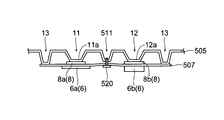
- the chassis 505 is provided with ribs 511 that protrude between the ribs 11 and 12 and protrude toward the substrate 507 (outside).
- the rib 511 has a protruding height smaller than that of the plurality of ribs 13.
- screw holes 511 a are formed in the rib 511.
- a screw thread may be formed in the screw hole 511a.
- the chassis 505 is an example of the “first metal plate” in the present invention.
- a screw hole 507e is formed in the center portion 507c of the substrate 507 at a position corresponding to the screw hole 511a of the chassis 505.
- Screws 520 are attached to the screw holes 507e (substrate 507) and the screw holes 511a (chassis 505), and the screws 520 provide a central portion 507c (element mounting portions 7a and 7b (see FIG. 14)) of the substrate 507.
- the intermediate portion is pressed to the chassis 505 side. For this reason, the center part 507c (the part between the element mounting parts 7a and 7b) of the substrate 507 is curved toward the chassis 505 side.
- the remaining structure of the sixth embodiment is similar to that of the aforementioned first embodiment.
- the ribs 11 and 12 are more reliably brought into contact with the substrate 507 (heat radiation sheet 8) by the screws 520. be able to.
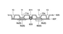
- a rib 611 that protrudes toward the substrate 607 (outside) is formed on the chassis 605 between the rib 11 and the rib 12.
- the rib 611 has a protruding height smaller than that of the plurality of ribs 13.
- a band attachment hole 611a is formed in the rib 611.
- the chassis 605 is an example of the “first metal plate” in the present invention.
- a band attachment hole 607e is formed in the central portion 607c of the substrate 607 in the vicinity of the band attachment hole 611a of the chassis 605.
- a band 620 is attached to the band attachment hole 607e and the band attachment hole 611a, and the center portion 607c of the substrate 607 (the portion between the element mounting portions 7a and 7b (see FIG. 17)) is the chassis by the band 620. It is pressed to the 605 side. For this reason, the center part 607c (the part between the element mounting parts 7a and 7b) of the substrate 607 is curved toward the chassis 605 side.
- the band 620 may be formed of, for example, a binding band such as a tie wrap (registered trademark) or a heat contraction band that contracts by heat.
- a binding band such as a tie wrap (registered trademark) or a heat contraction band that contracts by heat.
- the remaining structure of the seventh embodiment is similar to that of the aforementioned sixth embodiment.
- the ribs 11 and 12 are reliably brought into contact with the substrate 607 (heat radiation sheet 8) by the band 620. Can do.
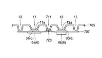
- a rib 711 that protrudes toward the substrate 707 (outside) is formed on the chassis 705 between the rib 11 and the rib 12.
- the rib 711 has a protruding height smaller than that of the plurality of ribs 13.
- the chassis 705 is an example of the “first metal plate” in the present invention.
- an adhesive layer 720 is disposed between the rib 711 and the substrate 707, and the central portion of the substrate 707 is bent toward the chassis 705 by the adhesive layer 720. For this reason, the substrate 707 is pressed against the ribs 11 and 12 of the chassis 705.
- the adhesive layer 720 is an example of the “first adhesive layer” in the present invention.
- the curvature of the substrate 707 is maintained by curing the adhesive layer 720 in a state where the central portion of the substrate 707 is curved toward the chassis 705.
- the remaining structure of the eighth embodiment is similar to that of the aforementioned sixth and seventh embodiments.
- the adhesive layer 720 that bonds the substrate 707 and the chassis 705 it is possible to suppress the chassis 705 from being separated from the substrate 707. It can be made to contact 707 (heat dissipation sheet 8) reliably.
- the chassis 805 corresponds to the ribs 11 and 12 protruding to the board 7 side (outside) and the edge 7 d (see FIG. 20) of the board 7 of the chassis 805. And a plurality of ribs 813 arranged at the positions.
- the chassis 805 is an example of the “first metal plate” in the present invention
- the rib 813 is an example of the “third projecting portion” in the present invention.
- an elastic body 820 for adjusting the distance from the chassis 805 (ribs 813, 11 and 12) to the substrate 7 is disposed between the rib 813 and the substrate 7.
- the elastic body 820 is made of, for example, silicone rubber, nylon, or urethane rubber, and can be elastically deformed.
- the elastic body 820 is an example of the “first elastic body” in the present invention.
- the rib 813 is formed with a screw hole 813a.
- a screw thread may be formed in the screw hole 813a.
- screw holes 820a and 7e are formed in the elastic body 820 and the substrate 7 at positions corresponding to the screw holes 813a of the chassis 805, respectively.
- screws 830 are attached to the screw holes 813 a, 820 a, and 7 e (see FIG. 20), and the board 7 is fixed to the chassis 805 together with the elastic body 820 by the screws 830. .
- the elastic body 820 is deformed (compressed) to a predetermined thickness by being tightened by a screw 830.
- the remaining structure of the ninth embodiment is similar to that of the aforementioned first to eighth embodiments.
- the elastic body 820 for adjusting the distance from the chassis 805 to the substrate 7 is provided between the rib 813 and the substrate 7. Thereby, since the distance from the ribs 11 and 12 to the board
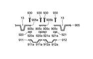
- the chassis 905 includes openings 905 a and 905 b formed around the portion to which the plurality of protruding members 911 and 912 are attached, and a plurality of ribs 13. .
- the chassis 905 is an example of the “first metal plate” in the present invention, and the protruding members 911 and 912 are examples of the “first protruding portion” in the present invention.
- a plurality of screw holes 905c are formed around the openings 905a and 905b of the chassis 905.
- projecting members 911 and 912 projecting toward the substrate 7 are attached to the chassis 905 so as to close the openings 905a and 905b.
- an elastic body 920 for adjusting the distance from the protruding member 911 to the chassis 905 is disposed between the protruding member 911 and the chassis 905.
- An elastic body 921 for adjusting the distance from the protruding member 912 to the chassis 905 is disposed between the protruding member 912 and the chassis 905.
- the elastic bodies 920 and 921 are made of, for example, silicone rubber, nylon or urethane rubber, and can be elastically deformed.
- the elastic bodies 920 and 921 are examples of the “second elastic body” in the present invention.
- screw holes 920a, 921a, 911a and 912a are formed in the elastic bodies 920 and 921 and the protruding members 911 and 912 at positions corresponding to the screw holes 905c of the chassis 905, respectively.
- screw holes may be formed in the screw holes 911a and 912a.
- screws 930 are attached to the screw holes 905c, 920a, 921a, 911a, and 912a (see FIG. 22), and the protruding members 911 and 912 are elastic bodies 920 by the screws 930, respectively. And 921 together with the chassis 905.
- the elastic bodies 920 and 921 are deformed (compressed) to a predetermined thickness by being tightened by the screws 930.
- the protruding members 911 and 912 are formed to have a thickness smaller than that of the chassis 905, but the protruding members 911 and 912 have the same thickness as the chassis 905 or a thickness larger than the chassis 905. It may be formed.
- the openings 905a and 905b may not be formed in the chassis 905.
- the protruding members 911 and 912 are attached to the chassis 905 via the elastic bodies 920 and 921, respectively. Thereby, since the distance from the protruding members 911 and 912 to the chassis 905 can be adjusted, the distance from the protruding members 911 and 912 to the substrate 7 can be adjusted. As a result, the contact pressure between the protruding members 911 and 912 and the substrate 7 can be adjusted.
- the display device is applied to a liquid crystal display device.
- the present invention is not limited thereto, and may be applied to a display device other than the liquid crystal display device.
- the electronic device is applied to a display device.
- the present invention is not limited thereto, and can be applied to various electronic devices such as a portable device, a household electric machine, or a solar battery. is there.
- the liquid crystal display device is formed by a direct-type backlight device.
- the present invention is not limited thereto, and the liquid crystal display device is formed by a sidelight-type backlight device. May be.
- the example in which the pressing member, the screw, the band, or the adhesive layer for bringing the semiconductor package into contact with the chassis has been provided.
- the present invention is not limited to this, and the semiconductor package is not limited to this.
- Two or more pressing members, screws, bands and adhesive layers for contacting the chassis may be used.
- heat conductive member was shown about the example formed with the heat radiating sheet (heat conductive sheet) which has high heat conductivity, this invention is not limited to this,
- a heat conductive member is high heat conduction. It may be formed by heat dissipation grease having a high rate (for example, silicone grease).
- the present invention is not limited to this, and the projecting member (first projecting portion). May be formed separately from the chassis and attached to the chassis.
- the projecting member (first projecting portion) can be formed using a material having good thermal conductivity such as copper or aluminum regardless of the material of the chassis.
- the through hole is formed in the contact portion.
- the present invention is not limited to this, and in other embodiments, the through hole may be formed in the contact portion.
- the present invention is not limited to this, and an adhesive tape is used. Even if the board (heat radiating sheet) is brought into contact with the chassis by pulling the board (heat radiating sheet) to the chassis side or pressing the board (heat radiating sheet) to the chassis side by using the attractive force or repulsive force of a magnet or the like Good.
- the present invention is not limited to this, and for example, the frame (electronic device) of the television receiver is used.
- the substrate may be pressed toward the chassis by a frame to be stored. In this case, since it is not necessary to provide a pressing member separately, the number of parts can be reduced.
- corrugated ribs 1005 a are formed in portions other than the protruding portions (first protruding portions, radiating fins) 1011 and 1012 and the ribs (third protruding portions) 1013 of the chassis 1005. May be. If comprised in this way, heat dissipation can be improved more. In this case, it is preferable to form the rib 1005a in the chassis 1005 around the protrusions 1011 and 1012.
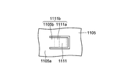
- the spring portion 1111b may be formed by a portion 1111a of the protruding portion (first protruding portion, radiating fin) 1111 and a portion 1105b of the flat portion 1105a.
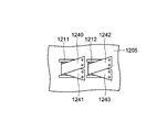
- a plate spring (first heat conducting member) is provided on the projecting portion (first projecting portion, radiating fin) 1211 of the chassis (first metal plate) 1205. 1240 and 1241 may be attached, and leaf springs (first heat conducting members) 1242 and 1243 may be attached to the protrusions (first protrusions, radiating fins) 1212.
- heat generated in each semiconductor package can be dissipated (transmitted) in three directions, so that heat dissipation can be further improved.
- the present invention is not limited to this, and a heat conducting member other than the leaf spring may be attached.
- a heat conducting member other than the leaf spring may be attached.
- metal tapes such as copper tape (projections (first protrusions, radiating fins) 1311 and 1312 of the chassis (first metal plate) 1305 are used.
- the first heat conducting member 1340 and 1341 may be attached respectively.
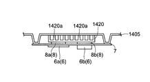
- the two heat radiating sheets 8 may be brought into contact with one heat radiating fin (first projecting portion) 1420 of the chassis (first metal plate) 1405.
- a plurality of heat radiation pieces 1420a may be provided on the heat radiation fin 1420.
- substrate and the 1st protrusion part was shown, this invention is not restricted to this, A board
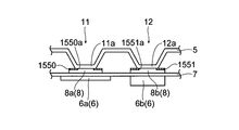
- the adhesive layers (second adhesive layers) 1550 and 1551 are disposed between the heat radiation sheet 8 (8a and 8b) and the ribs 11 and 12. May be arranged.
- openings 1550a and 1551a may be formed in the central portions of the adhesive layers 1550 and 1551, respectively, and the adhesive layers 1550 and 1551 may be disposed only in the peripheral portions of the heat radiation sheet 8 (8a and 8b). .
- the openings 1550a and 1551a may not be formed in the adhesive layers 1550 and 1551, and the adhesive layers 1550 and 1551 may be disposed on the entire surface of the heat dissipation sheet 8 (8a and 8b).
- the adhesive layers 1550 and 1551 can be easily formed by, for example, applying an adhesive or applying a double-sided tape to the heat dissipation sheet 8 (8a and 8b).
- the contact portion 1611a of the protruding portion (first protruding portion, radiating fin) 1611 is curved so as to protrude toward the radiating sheet side (substrate side). May be.
- the contact portion 1611a may be formed in a corrugated shape or a hemispherical shape.
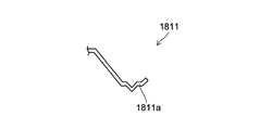
- the contact portion 1811a of the protrusion (first protrusion, radiating fin) 1811 may be formed in a mountain shape (triangular pyramid). If comprised as mentioned above, the contact part of a 1st protrusion part can be made to carry out a line contact or a point contact to the desired position (for example, high temperature part) of a board
- the present invention is not limited to this, for example, the tenth modification of the present invention shown in FIG.
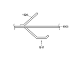
- the radiation fins 1920 may be attached in the vicinity of the protrusions (first protrusions, heat radiation fins) 1911 of the chassis (first metal plate) 1905. In this case, it is preferable to attach the radiation fins 1920 in the vicinity of the root portion of the protruding portion 1911 in the chassis 1905.
- a box-shaped (rib-shaped) heat dissipation plate 2020 may be attached in the vicinity of the protruding portion 1911 of the chassis 1905 as in the eleventh modification of the present invention shown in FIG.
- a protruding portion is formed by cutting out and bending a part of the chassis and a radiating fin or a radiating plate is attached to the chassis is shown.
- the part may form a heat radiating fin or a heat radiating rib, and the protrusion may be attached to the chassis.
- a heat radiating piece may be provided on the heat radiating fin.
- a radiating piece 2120a may be provided on the radiating fin 2120 as in the twelfth modification of the present invention shown in FIG.
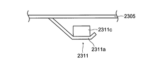
- the heat radiating piece 2211c. 37 as in the fourteenth modification of the present invention shown in FIG. 37, for example, the contact portion 2311a of the protruding portion (first protruding portion, radiating fin) 2311 of the chassis (first metal plate) 2305.
- a heat radiating piece 2311c may be provided. Note that these heat radiation pieces may be formed by bending a part of the heat radiation fins, or the heat radiation pieces may be attached to the heat radiation fins.
- the first protrusion (rib, protrusion) is formed in the chassis and the heat generated in the semiconductor package is radiated to the chassis.
- the present invention is not limited to this.
- a metal plate (first metal plate) 2420 is provided outside the chassis 2405, and the heat radiation sheet 8 is attached to the ribs (first protrusions) 2411 and 2412 of the metal plate 2420. By making the contact, the heat generated in the semiconductor package 6 may be radiated to the metal plate 2420.
- the metal plate 2420 is attached to the chassis 2405 using a screw or the like (not shown).
- the attachment surface of the substrate 7 may be attached to the chassis (second metal plate) 2505.
- a metal plate (first metal plate) 2520 may be provided on the opposite side (outside) of the substrate 7 from the chassis 2505.
- Liquid crystal display device (electronic equipment, display device) 5, 105, 205, 305, 505, 605, 705, 805, 905, 1005, 1205, 1305, 1405, 1905, 2205, 2305 Chassis (first metal plate) 6, 6a, 6b Semiconductor package 7, 507, 607, 707 Substrate 7d, 507d Edge 8, 8a, 8b Heat radiation sheet (first heat conducting member) 11, 12, 311, 2411, 2412 rib (first protrusion) 13, 813, 1013 Rib (third protrusion) 105b, 105c, 205b, 205c Cutout portion 111, 112, 211, 212, 1011, 1012, 1111, 1211, 1212, 1311, 1312, 1611, 1711, 1811, 1911, 2111, 2311 Protruding portion (first protruding portion, Heat dissipation fin) 111a, 112a, 211a, 212a, 1611a, 1711a, 1811a, 2111
Landscapes
- Physics & Mathematics (AREA)
- Nonlinear Science (AREA)
- Mathematical Physics (AREA)
- Chemical & Material Sciences (AREA)
- Crystallography & Structural Chemistry (AREA)
- General Physics & Mathematics (AREA)
- Optics & Photonics (AREA)
- Thermal Sciences (AREA)
- Engineering & Computer Science (AREA)
- Microelectronics & Electronic Packaging (AREA)
- Cooling Or The Like Of Electrical Apparatus (AREA)
- Cooling Or The Like Of Semiconductors Or Solid State Devices (AREA)
Abstract
放熱性が低下するのを抑制することが可能な電子機器を提供する。この液晶表示装置(電子機器)(1)は、半導体パッケージ(6)と、半導体パッケージが取り付けられる取付面を有する基板(7)と、基板の取付面とは反対側の面に対向配置され、基板側に突出するリブ(11および12)が設けられたシャーシ(5)と、シャーシのリブと基板との間に配置される放熱シート(8)とを備える。
Description
この発明は、電子機器および表示装置に関し、特に、半導体パッケージが取り付けられた基板を備えた電子機器および表示装置に関する。
従来、半導体パッケージが取り付けられた基板を備えた電子機器が知られている。図40は、半導体パッケージが取り付けられた基板を備えた従来の一例による電子機器の構造を示した断面図である。
従来の一例による電子機器5001は、図40に示すように、複数の半導体パッケージ5002と、複数の半導体パッケージ5002が取り付けられた基板5003と、半導体パッケージ5002上に配置された放熱シート5004と、放熱シート5004を介して半導体パッケージ5002に接触される金属板5005と、基板5003から所定の距離を隔てて配置されるシャーシ5006とを備えている。
複数の半導体パッケージ5002は、互いに異なる厚みを有する半導体パッケージ5002aおよび5002bを含んでいる。例えば、半導体パッケージ5002bは、半導体パッケージ5002aよりも大きい厚みを有する。
複数の放熱シート5004は、半導体パッケージ5002a上に配置される放熱シート5004aと、半導体パッケージ5002b上に配置される放熱シート5004bとを含んでいる。例えば、放熱シート5004bは、放熱シート5004aよりも小さい厚みを有する。
そして、半導体パッケージ5002aは、放熱シート5004aを介して金属板5005に接触されており、半導体パッケージ5002bは、放熱シート5004bを介して金属板5005に接触されている。これにより、半導体パッケージ5002で発生する熱を金属板5005に放熱させることが可能である。
また、シャーシ5006には、図示しない固定部材を用いて、基板5003および金属板5005が固定されている。
なお、半導体パッケージで発生する熱を金属板に放熱させる構造は、例えば、特許文献1および特許文献2に開示されている。
しかしながら、従来の一例による電子機器5001では、製造ばらつきなどにより、金属板5005が、半導体パッケージ5002(放熱シート5004)に接触しない場合がある。
例えば、図41に示すように、製造ばらつきにより、半導体パッケージ5002aの取付高さ(基板5003の取付面から半導体パッケージ5002aの上面までの距離)が設計値よりも小さくなった場合、金属板5005が半導体パッケージ5002a(放熱シート5004a)に接触しなくなる場合がある。このため、半導体パッケージ5002aで発生する熱を金属板5005に放熱させることが困難であるという問題点がある。
この発明は、上記のような課題を解決するためになされたものであり、この発明の目的は、放熱性が低下するのを抑制することが可能な電子機器および表示装置を提供することである。
上記目的を達成するために、この発明の第1の局面による電子機器は、半導体パッケージと、半導体パッケージが取り付けられる取付面を有する基板と、基板の取付面とは反対側の面に対向配置され、基板側に突出する第1突出部が設けられた第1金属板と、第1金属板の第1突出部および基板の間に配置される第1熱伝導部材とを備える。
この第1の局面による電子機器では、上記のように、基板の取付面とは反対側の面に対向配置される第1金属板と、第1金属板の第1突出部および基板の間に配置される第1熱伝導部材とを設けることによって、半導体パッケージで発生する熱を、基板および第1熱伝導部材を介して第1金属板に放熱させることができる。
また、第1の局面による電子機器では、製造ばらつきにより、半導体パッケージの取付高さ(基板の取付面から半導体パッケージの外面(例えば上面)までの距離)が設計値よりも小さくなった場合であっても、第1突出部から基板までの距離は変化しないので、第1突出部が基板(第1熱伝導部材)に接触しなくなるのを抑制することができる。これにより、電子機器の放熱性が低下するのを抑制することができる。
また、第1の局面による電子機器では、上記のように、第1金属板に、基板側に突出する第1突出部を設けることによって、第1熱伝導部材の厚みを小さくすることができる。これにより、電子機器の放熱性を向上させることができるとともに、第1熱伝導部材のコストを低減することができる。
また、第1の局面による電子機器では、半導体パッケージで発生する熱を、基板の背面(取付面とは反対側の面)側に放熱させることができるので、半導体パッケージで発生する熱を基板の取付面側に放熱させる場合と異なり、基板の取付面側に放熱部材等を設けなくてもよい。これにより、電子機器全体が大型化するのを抑制することも可能である。
上記第1の局面による電子機器において、好ましくは、第1突出部は、第1熱伝導部材を介して基板に接触される接触部と、接触部を基板側に付勢するバネ部とを含む。このように構成すれば、バネ部により、接触部を基板側に付勢することができるので、接触部を基板(第1熱伝導部材)に、より確実に接触させることができる。
上記第1突出部が接触部とバネ部とを含む電子機器において、好ましくは、第1突出部は、第1金属板を折り曲げることにより形成されている。このように構成すれば、第1金属板に、基板側に突出する第1突出部を容易に形成することができるとともに、第1突出部に、接触部を基板側に付勢するバネ部を容易に形成することができる。
上記第1突出部が接触部とバネ部とを含む電子機器において、好ましくは、第1金属板の第1突出部の周囲には、切抜き部が形成されている。このように構成すれば、第1金属板を折り曲げることにより、第1突出部を容易に形成することができる。また、第1突出部を、第1金属板の所望の位置に形成することができる。
上記第1金属板の第1突出部の周囲に切抜き部が形成されている電子機器において、好ましくは、第1金属板には、切抜き部を跨ぎ、かつ、第1突出部と第1金属板の第1突出部以外の部分とに接触される第2熱伝導部材が設けられている。第1突出部の周囲に切抜き部が形成されている場合、半導体パッケージ(第1熱伝導部材)からの熱は、切抜き部が形成されていない方向に伝達(放熱)されるが、上記のように、切抜き部を跨ぎ、かつ、第1突出部と第1金属板の第1突出部以外の部分とに接触される第2熱伝導部材を設けることによって、半導体パッケージ(第1熱伝導部材)からの熱を、切抜き部が形成されていない方向と、切抜き部が形成されている方向(第2熱伝導部材が設けられた方向)とに伝達(放熱)させることができる。これにより、電子機器の放熱性を向上させることができる。
上記第1の局面による電子機器において、好ましくは、基板の取付面側に配置される第2金属板と、第2金属板および半導体パッケージの間に配置される第3熱伝導部材とをさらに備える。このように構成すれば、半導体パッケージで発生する熱を、第3熱伝導部材を介して第2金属板にも放熱させることができる。これにより、電子機器の放熱性をより向上させることができる。
上記第2金属板と第3熱伝導部材とを備える電子機器において、好ましくは、第2金属板は、第3熱伝導部材および半導体パッケージを介して、基板を第1金属板側に押圧する機能を有する。このように構成すれば、第2金属板が第3熱伝導部材に接触しなくなるのを抑制することができるとともに、第1突出部(第1金属板)が第1熱伝導部材に接触しなくなるのを抑制することができる。これにより、電子機器の放熱性が低下するのをより抑制することができる。
上記第2金属板と第3熱伝導部材とを備える電子機器において、好ましくは、第2金属板は、半導体パッケージ側に突出するとともに第3熱伝導部材に接触する第2突出部を含む。このように構成すれば、例えば、基板に、互いに異なる厚みを有する複数の半導体パッケージが取り付けられている場合にも、複数の第2突出部の各々の突出高さを、接触される半導体パッケージの厚みに合わせて設定することにより、全ての半導体パッケージを第2金属板(第2突出部)に容易に接触させることができる。
また、第2金属板に、半導体パッケージ側に突出する第2突出部を設けることによって、第3熱伝導部材の厚みを小さくすることができる。これにより、電子機器の放熱性を向上させることができるとともに、第3熱伝導部材のコストを低減することができる。
上記第1の局面による電子機器において、好ましくは、半導体パッケージおよび第1熱伝導部材は、それぞれ、複数設けられており、複数の第1熱伝導部材のうちの少なくとも2つの第1熱伝導部材は、互いに同じ厚みに形成されているとともに、1つの第1突出部に接触されている。このように、半導体パッケージおよび第1熱伝導部材が、それぞれ、複数設けられている場合であっても、第1の局面による電子機器では、複数の半導体パッケージが互いに異なる厚みを有するか否かにかかわらず、複数の第1熱伝導部材のうちの少なくとも2つの第1熱伝導部材を、互いに同じ厚みに形成し、かつ、1つの第1突出部に接触させることができる。
上記第1の局面による電子機器において、好ましくは、第1金属板には、放熱フィンが設けられている。このように構成すれば、電子機器の放熱性をより向上させることができる。
上記第1金属板に放熱フィンが設けられている電子機器において、好ましくは、放熱フィンは、第1金属板を切り抜くことにより形成されている。このように構成すれば、第1金属板に、容易に放熱フィンを形成することができる。
上記第1の局面による電子機器において、好ましくは、第1突出部は、第1熱伝導部材を介して基板に接触される接触部を含み、接触部には、貫通孔が形成されている。このように構成すれば、基板を第1金属板に取り付ける際に、基板の取付面とは反対側の面上に第1熱伝導部材が配置されているか否かを、第1金属板側から確認することができる。
上記第1の局面による電子機器において、好ましくは、基板と第1金属板とに取り付けられるとともに、基板の中央部を第1金属板側に押圧するネジおよびバンドの少なくとも一方をさらに備える。このように構成すれば、第1突出部を基板(第1熱伝導部材)に、より確実に接触させることができる。
上記第1の局面による電子機器において、好ましくは、基板と第1金属板とを接着する第1接着層をさらに備える。このように構成すれば、第1金属板が基板から離れるのを抑制することができるので、第1突出部を基板(第1熱伝導部材)に、より確実に接触させることができる。
上記第1の局面による電子機器において、好ましくは、第1金属板の、基板の縁部に対応する位置には、基板側に突出する第3突出部が設けられており、基板の縁部は、第1金属板の第3突出部に取り付けられている。このように構成すれば、基板の中央部と第1金属板との間に隙間を形成することができる。
上記第1金属板に第3突出部が設けられている電子機器において、好ましくは、第3突出部と基板との間には、第1金属板から基板までの距離を調節するための第1弾性体が設けられている。このように構成すれば、第1突出部から基板までの距離を調節することができるので、第1突出部と基板との接触圧を調節することができる。
上記第1の局面による電子機器において、好ましくは、第1突出部は、第1突出部から第1金属板までの距離を調節するための第2弾性体を介して、第1金属板に取り付けられている。このように構成すれば、第1突出部から第1金属板までの距離を調節することができるので、第1突出部から基板までの距離を調節することができる。これにより、第1突出部と基板との接触圧を調節することができる。
上記第1の局面による電子機器において、好ましくは、第1熱伝導部材と第1突出部との間には、第2接着層が配置されている。このように構成すれば、第1熱伝導部材と第1突出部との接触を良好に保つことができるので、半導体パッケージで発生する熱を第1突出部に、より伝達(放熱)させやすくすることができる。これにより、電子機器の放熱性をより向上させることができる。
この発明の第2の局面による表示装置は、上記の構成の電子機器を備える。このように構成すれば、放熱性が低下するのを抑制することが可能な表示装置を得ることができる。
以上のように、本発明によれば、放熱性が低下するのを抑制することが可能な電子機器および表示装置を容易に得ることができる。
以下、本発明の実施形態について図面を参照して説明する。なお、理解を容易にするために、断面図であってもハッチングを施さない場合や、平面図であってもハッチングを施す場合もある。
(第1実施形態)
図1~図3を参照して、本発明の第1実施形態による液晶表示装置1の構造について説明する。
図1~図3を参照して、本発明の第1実施形態による液晶表示装置1の構造について説明する。
本発明の第1実施形態による液晶表示装置1は、例えば液晶テレビジョン受像機(図示せず)などを構成するものである。また、液晶表示装置1は、図1に示すように、液晶表示パネル2と、液晶表示パネル2の裏面(背面)側に配置される光学シート3および複数の光源4と、光学シート3および複数の光源4を収納する板金製のシャーシ5と、シャーシ5の外部に配置される複数の半導体パッケージ6と、複数の半導体パッケージ6が取り付けられシャーシ5に対向配置された基板7と、シャーシ5および基板7の間に配置された放熱シート(熱伝導シート)8とによって構成されている。そして、光学シート3、複数の光源4およびシャーシ5などによって、直下型のバックライト装置が構成されている。なお、液晶表示装置1は、本発明の「電子機器」および「表示装置」の一例であり、シャーシ5は、本発明の「第1金属板」の一例である。また、放熱シート8(8a、8b))は、本発明の「第1熱伝導部材」の一例である。
液晶表示パネル2は、図示しない液晶層を挟み込む2つのガラス基板からなる。また、液晶表示パネル2は、光源4に照明されることにより、表示パネルとして機能する。
光学シート3は、例えば、プリズムシートやレンズシートなどの複数のシート類により構成されている。
光源4は、例えば、蛍光ランプにより形成されている。なお、光源4は、蛍光ランプ以外の、例えばLED(Light Emitting Diode)などにより形成されていてもよい。また、光源4の背面側に、反射シート(図示せず)が配置されていてもよい。
ここで、第1実施形態では、図2に示すように、シャーシ5には、基板7側(外側)に突出する複数のリブ10が形成されている。この複数のリブ10は、例えば、絞り加工により形成されている。
また、複数のリブ10は、放熱シート8を介して半導体パッケージ6に接触されるリブ11および12と、複数のリブ13とを含んでいる。なお、リブ11および12は、本発明の「第1突出部」の一例であり、リブ13は、本発明の「第3突出部」の一例である。
リブ11および12は、互いに同じ突出高さ(厚み方向の高さ)を有するように形成されている。
また、リブ11は、後述する半導体パッケージ6aに対応する位置(基板7の後述する素子搭載部7a(図3参照)に対向する位置)に形成されており、リブ12は、後述する半導体パッケージ6bに対応する位置(基板7の後述する素子搭載部7b(図3参照)に対向する位置)に形成されている。また、リブ11および12には、放熱シート8を介して基板7に接触される接触部11aおよび12aがそれぞれ形成されている。この接触部11aおよび12aは、例えば平坦に形成されている。
複数のリブ13は、シャーシ5の基板7の後述する縁部7d(図3参照)に対応する位置(縁部7dの真上の位置)に配置されている。また、複数のリブ13は、互いに同じ突出高さを有するように形成されている。また、複数のリブ13は、リブ11および12よりも大きい突出高さを有している。また、複数のリブ13の突出高さは、リブ11(またはリブ12)の突出高さと、後述する放熱シート8a(または放熱シート8b)の厚みとを合わせた値と同程度の大きさに設定されている。
複数の半導体パッケージ6は、例えば、FRC(Frame Rate Control)などの処理を行うための素子であり、動作中の発熱量が多い。また、複数の半導体パッケージ6は、互いに異なる厚みを有する半導体パッケージ6aおよび6bを含んでいる。例えば、半導体パッケージ6bは、半導体パッケージ6aよりも大きい厚みを有する。
また、複数の半導体パッケージ6aおよび6bは、図示しない半田層などを用いて、基板7の取付面に取り付けられている。なお、半導体パッケージ6bの取付高さ(基板7の取付面から半導体パッケージ6bの外面(図2の下側の面)までの距離)H2は、半導体パッケージ6aの取付高さ(基板7の取付面から半導体パッケージ6aの外面(図2の下側の面)までの距離)H1よりも大きい。
基板7は、図3に示すように、複数の半導体パッケージ6aおよび6bがそれぞれ取り付けられる素子搭載部7aおよび7bを含む中央部7cと、縁部7d(中央部7c以外の部分とを含む。
また、基板7には、図示しない半田層などを介して、半導体パッケージ6aおよび6bで発生した熱が伝達される。また、基板7の素子搭載部7aおよび7bには、基板7の厚み方向に熱を伝導するために、金属材料が充填されたスルーホール(図示せず)が設けられていてもよい。
また、図2に示すように、基板7の縁部7dの裏面(取付面とは反対側の面)は、図示しないネジなどを用いて、シャーシ5のリブ13に固定されている。
放熱シート8は、高い熱伝導率を有するシート部材により形成されている。また、放熱シート8は、押圧されることにより圧縮するように、弾性変形可能に形成されている。具体的には、放熱シート8は、シリコーンゴムやアクリルゴムなどにより形成されており、放熱シート8のアスカーC硬度は、例えば、10~60程度である。
また、複数の放熱シート8は、基板7の素子搭載部7aの裏面上に配置される放熱シート8aと、基板7の素子搭載部7bの裏面上に配置される放熱シート8bとを含んでいる。
そして、基板7の素子搭載部7aは、放熱シート8aを介してリブ11の接触部11aに接触されており、基板7の素子搭載部7bは、放熱シート8bを介してリブ12の接触部12aに接触されている。
第1実施形態では、上記のように、シャーシ5のリブ11および12と基板7との間に、放熱シート8を設けることによって、半導体パッケージ6で発生する熱を、基板7および放熱シート8(8aおよび8b)を介してシャーシ5に放熱させることができる。
また、第1実施形態では、例えば、製造ばらつきにより、半導体パッケージ6(6aおよび6b)の取付高さが設計値よりも小さくなった場合であっても、リブ11および12から基板7までの距離は変化しないので、リブ11および12が基板7(放熱シート8)に接触しなくなるのを抑制することができる。これにより、液晶表示装置1の放熱性が低下するのを抑制することができる。
また、第1実施形態では、上記のように、シャーシ5に、基板7側に突出するリブ11および12を設けることによって、放熱シート8(8aおよび8b)の厚みを小さくすることができる。これにより、液晶表示装置1の放熱性を向上させることができるとともに、放熱シート8(8aおよび8b)のコストを低減することができる。
また、第1実施形態では、半導体パッケージ6で発生する熱を、基板7の背面(取付面とは反対側の面)側に放熱させることができるので、半導体パッケージ6で発生する熱を基板7の取付面側に放熱させる場合と異なり、基板7の取付面側に放熱部材等を設けなくてもよい。これにより、液晶表示装置1全体が大型化するのを抑制することも可能である。
第1実施形態では、上記のように、シャーシ5の、基板7の縁部7dに対応する位置に、基板7側に突出するリブ13を設け、基板7の縁部7dを、シャーシ5のリブ13に取り付ける。これにより、基板7の中央部7cとシャーシ5との間に隙間を形成することができる。
また、第1実施形態では、半導体パッケージ6は発熱量が多いので、液晶表示装置1を上記のように構成することは、特に有効である。
(第2実施形態)
この第2実施形態では、図4~図7を参照して、上記第1実施形態と異なり、基板7(放熱シート8)を接触部111aおよび112aに接触させるために、バネ部111bおよび112bを設ける場合について説明する。
この第2実施形態では、図4~図7を参照して、上記第1実施形態と異なり、基板7(放熱シート8)を接触部111aおよび112aに接触させるために、バネ部111bおよび112bを設ける場合について説明する。
第2実施形態では、図4に示すように、シャーシ105には、基板7側(外側)に突出する複数の突出部111および112と、複数のリブ13と、放熱フィンとして機能する複数のフィン部113および114とが形成されている。なお、シャーシ105は、本発明の「第1金属板」の一例であり、突出部111および112は、本発明の「第1突出部」および「放熱フィン」の一例である。また、フィン部113および114は、本発明の「放熱フィン」の一例である。
複数の突出部111および112は、放熱シート8を介して基板7に接触される。また、複数の突出部111および112は、互いに同じ突出高さを有するように形成されている。
また、突出部111は、半導体パッケージ6aに対応する位置(基板7の素子搭載部7aに対向する位置)に形成されており、突出部112は、半導体パッケージ6bに対応する位置(基板7の素子搭載部7bに対向する位置)に形成されている。
ここで、第2実施形態では、突出部111は、半導体パッケージ6(放熱シート8)に接触される接触部111aと、接触部111aを基板7側に付勢するバネ部111bとを含んでいる。このバネ部111bは、接触部111aと、シャーシ105の平面部105a(シャーシ105のうちの、突出部111、112、リブ13、フィン部113および114以外の部分)とを接続している。
同様に、突出部112は、半導体パッケージ6(放熱シート8)に接触される接触部112aと、接触部112aを基板7側に付勢するバネ部112bとを含んでいる。このバネ部112bは、接触部112aと、シャーシ105の平面部105aとを接続している。
また、突出部111および112は、シャーシ105の一部を切り抜き、折り曲げることにより形成されている。具体的には、図5に示すように、突出部111および112の周囲には、例えばコの字形状の切抜き部105bおよび105cがそれぞれ形成されている。そして、図5の破線の位置で折り曲げることにより、突出部111および112が形成されている。
また、第2実施形態では、図6に示すように、突出部111の接触部111aは、基板7がシャーシ105に固定されていない状態で、放熱シート8aの上面(前面)が配置される予定の位置よりも外側(下側)に位置するように形成されている。これにより、基板7がシャーシ105に固定された状態(図4の状態)で、接触部111aを放熱シート8a(基板7)に、より確実に接触させることが可能である。
なお、基板7がシャーシ105に固定された状態では、突出部111のバネ部111bが弾性変形するので、接触部111aの放熱シート8a(基板7)に対する接触圧が大きくなりすぎるのを抑制することが可能である。
同様に、突出部112の接触部112aは、基板7がシャーシ105に固定されていない状態で、放熱シート8bの上面(前面)が配置される予定の位置よりも外側(下側)に位置するように形成されている。これにより、基板7がシャーシ105に固定された状態で、接触部112aを放熱シート8b(基板7)に、より確実に接触させることが可能である。
なお、基板7がシャーシ105に固定された状態では、突出部112のバネ部112bが弾性変形するので、接触部112aの放熱シート8b(基板7)に対する接触圧が大きくなりすぎるのを抑制することが可能である。
また、図7に示すように、接触部111aおよび112aには、貫通孔111cおよび112cがそれぞれ形成されていてもよい。なお、貫通孔111cおよび112cは、円形状であってもよいし、三角形状、四角形状またはその他の形状であってもよい。
また、複数のフィン部113および114は、シャーシ105の一部を切り抜き、折り曲げることにより形成されている。具体的には、図5に示すように、フィン部113および114の周囲には、例えばコの字形状の切抜き部105dおよび105eがそれぞれ形成されている。そして、図5の2点鎖線の位置で折り曲げることにより、フィン部113および114が形成されている。
また、フィン部113および114を折り曲げることによって、フィン部113および114とシャーシ105の平面部105aとの隙間が大きくなるので、空気の通り(空気の流れ)が良くなる。そして、空気の通りの良い部分にフィン部113および114を設けることになるので、放熱性をより向上させることが可能になる。
また、第2実施形態では、突出部111および112の周囲にも隙間が形成されているとともに、突出部111および112も放熱フィンとして機能する。
なお、放熱性をさらに向上させたい場合には、放熱ファン(図示せず)を別途設けてもよい。この場合、突出部111および112や、フィン部113および114に直接風が当たるように、放熱ファンを配置することが好ましい。
なお、第2実施形態のその他の構造は、上記第1実施形態と同様である。
第2実施形態では、上記のように、突出部111および112に、放熱シート8を介して基板7に接触される接触部111aおよび112aと、接触部111aおよび112aを基板7側に付勢するバネ部111bおよび112bとを設ける。これにより、バネ部111bおよび112bにより、接触部111aおよび112aを基板7側に付勢することができるので、接触部111aおよび112aを基板7(放熱シート8)に、より確実に接触させることができる。
また、第2実施形態では、上記のように、シャーシ105を折り曲げることにより突出部111および112を形成する。これにより、シャーシ105に、基板7側に突出する突出部111および112を容易に形成することができるとともに、突出部111および112に、接触部111aおよび112aを基板7側に付勢するバネ部111bおよび112bを容易に形成することができる。
また、第2実施形態では、上記のように、シャーシ105の突出部111および112の周囲に、切抜き部105bおよび105cを形成することによって、シャーシ105を折り曲げることにより、突出部111および112を容易に形成することができる。また、突出部111および112を、シャーシ105の所望の位置に形成することができる。
また、第2実施形態では、上記のように、シャーシ105に、フィン部113および114を設けることによって、液晶表示装置の放熱性をより向上させることができる。
さらに、第2実施形態では、突出部111および112も放熱フィンとして機能するので、液晶表示装置の放熱性をさらに向上させることができる。
また、第2実施形態では、上記のように、接触部111aおよび112aに、貫通孔111cおよび112cを形成することによって、基板7をシャーシ105に取り付ける際に、基板7の取付面とは反対側の面上に放熱シート8(8aおよび8b)が配置されているか否かを、シャーシ105側から確認することができる。
なお、第2実施形態のその他の効果は、上記第1実施形態と同様である。
(第3実施形態)
この第3実施形態では、図8および図9を参照して、上記第2実施形態と異なり、シャーシ205に板バネ220および221が取り付けられている場合について説明する。
この第3実施形態では、図8および図9を参照して、上記第2実施形態と異なり、シャーシ205に板バネ220および221が取り付けられている場合について説明する。
第3実施形態では、図8に示すように、シャーシ205には、基板7側(外側)に突出する複数の突出部211および212と、複数のリブ13と、複数のフィン部113および114とが形成されている。なお、シャーシ205は、本発明の「第1金属板」の一例であり、突出部211および212は、本発明の「第1突出部」および「放熱フィン」の一例である。
複数の突出部211および212は、互いに同じ突出高さを有するように形成されている。
また、突出部211は、半導体パッケージ6aに対応する位置に形成されており、突出部212は、半導体パッケージ6bに対応する位置に形成されている。
また、突出部211は、接触部211aと、接触部211aを基板7側に付勢するバネ部211bとを含んでいる。同様に、突出部212は、接触部212aと、接触部212aを基板7側に付勢するバネ部212bとを含んでいる。
また、図9に示すように、突出部211および212の周囲には、コの字形状の切抜き部205bおよび205cがそれぞれ形成されており、突出部211および212は、シャーシ205の一部を湾曲させることにより形成されている。
ここで、第3実施形態では、シャーシ205の所定領域には、例えば銅やアルミニウムなどにより形成された板バネ220および221が取り付けられている。なお、板バネ220および221は、本発明の「第2熱伝導部材」の一例である。
具体的には、板バネ220は、切抜き部205bを跨ぐように配置されている。また、板バネ220は、湾曲されており、突出部211と放熱シート8(基板7)とに挟まれるように形成されている。
また、板バネ220は、例えば溶接部220aがスポット溶接されることにより、シャーシ205の平面部205a(シャーシ205のうちの、突出部211、212、リブ13、フィン部113および114以外の部分)に固定されている。そして、板バネ220は、突出部211と、シャーシ205の平面部205aとに接触される。なお、平面部205aは、本発明の「第1金属板の第1突出部以外の部分」の一例である。
同様に、板バネ221は、切抜き部205cを跨ぐように配置されている。また、板バネ221は、湾曲されており、突出部212と放熱シート8(基板7)とに挟まれるように形成されている。
また、板バネ221は、例えば溶接部221aがスポット溶接されることにより、シャーシ205の平面部205aに固定されている。そして、板バネ221は、突出部212と、シャーシ205の平面部205aとに接触される。
また、板バネ220および221は、基板7がシャーシ205に固定されていない状態で、放熱シート8の上面(前面)が配置される予定の位置よりも外側(下側)に位置するように形成されている。これにより、基板7がシャーシ205に固定された状態で、接触部211aを、板バネ220を介して放熱シート8(基板7)に確実に接触させることが可能であるとともに、接触部212aを、板バネ221を介して放熱シート8(基板7)に確実に接触させることが可能である。
また、図では、板バネ220および221は、平面的に見て長方形状に形成されているが、三角形状、円状または多角形状等に形成されていてもよい。
また、突出部211を、板バネ220と放熱シート8(基板7)とに挟まれるように配置してもよい。同様に、突出部212を、板バネ221と放熱シート8(基板7)とに挟まれるように配置してもよい。
なお、第3実施形態のその他の構造は、上記第1および第2実施形態と同様である。
第3実施形態では、上記のように、シャーシ205に、切抜き部205bを跨ぎ、かつ、突出部211とシャーシ205の平面部205aとに接触される板バネ220を設ける。ここで、突出部211の周囲に切抜き部205bが形成されている場合、半導体パッケージ6a(放熱シート8a)からの熱は、切抜き部205bが形成されていない方向に伝達(放熱)されるが、上記のように、切抜き部205bを跨ぐように板バネ220を設けることによって、半導体パッケージ6a(放熱シート8a)からの熱を、切抜き部205bが形成されていない方向と、切抜き部205bが形成されている方向(板バネ220が設けられた方向)とに伝達(放熱)させることができる。これにより、液晶表示装置の放熱性を向上させることができる。
同様に、シャーシ205に、切抜き部205cを跨ぎ、かつ、突出部212とシャーシ205の平面部205aとに接触される板バネ221を設ける。ここで、突出部212の周囲に切抜き部205cが形成されている場合、半導体パッケージ6b(放熱シート8b)からの熱は、切抜き部205cが形成されていない方向に伝達(放熱)されるが、上記のように、切抜き部205cを跨ぐように板バネ221を設けることによって、半導体パッケージ6b(放熱シート8b)からの熱を、切抜き部205cが形成されていない方向と、切抜き部205cが形成されている方向(板バネ221が設けられた方向)とに伝達(放熱)させることができる。これにより、液晶表示装置の放熱性を向上させることができる。
なお、第3実施形態のその他の効果は、上記第1および第2実施形態と同様である。
(第4実施形態)
この第4実施形態では、図10を参照して、上記第1~第3実施形態と異なり、複数の放熱シート8が1つのリブ311に接触されている場合について説明する。
この第4実施形態では、図10を参照して、上記第1~第3実施形態と異なり、複数の放熱シート8が1つのリブ311に接触されている場合について説明する。
第4実施形態では、図10に示すように、シャーシ305には、基板7側(外側)に突出するリブ311と、複数のリブ13とが形成されている。なお、シャーシ305は、本発明の「第1金属板」の一例であり、リブ311は、本発明の「第1突出部」の一例である。
また、リブ311は、例えば上記第1実施形態のリブ11とリブ12とを1つにしたように形成されている。具体的には、リブ311は、半導体パッケージ6aおよび6bに対応する位置に形成されている。また、リブ311には、放熱シート8aおよび8bに接触される接触部311aが形成されている。この接触部311aは、基板7と平行になるように形成されている。
なお、第4実施形態のその他の構造は、上記第1実施形態と同様である。
第4実施形態では、上記のように、放熱シート8aおよび8bを、互いに同じ厚みに形成し、1つのリブ311に接触させる。このように、放熱シート8aおよび8bが、それぞれ、複数設けられている場合であっても、第4実施形態では、複数の放熱シート8aおよび8bを、互いに同じ厚みに形成し、かつ、1つのリブ311に接触させることができる。
なお、第4実施形態のその他の効果は、上記第1実施形態と同様である。
(第5実施形態)
この第5実施形態では、図11を参照して、上記第1~第4実施形態と異なり、半導体パッケージ6の下側(基板7とは反対側)からも放熱させる場合について説明する。
この第5実施形態では、図11を参照して、上記第1~第4実施形態と異なり、半導体パッケージ6の下側(基板7とは反対側)からも放熱させる場合について説明する。
第5実施形態では、図11に示すように、基板7の取付面側に、板金製の押さえ部材420が設けられているとともに、半導体パッケージ6と押さえ部材420との間に、放熱シート440が配置されている。なお、押さえ部材420は、本発明の「第2金属板」の一例である。なお、放熱シート440(440a、440b)は、本発明の「第3熱伝導部材」の一例である。
押さえ部材420は、放熱シート440および半導体パッケージ6を介して、基板7をシャーシ5側に押圧する機能を有する。また、押さえ部材420には、基板7側(内側)に突出する複数のリブ430が形成されている。この複数のリブ430は、例えば、絞り加工により形成されている。
また、複数のリブ430は、放熱シート440を介して半導体パッケージ6に接触されるリブ431および432と、押さえ部材420の基板7の縁部7dに対応する位置に配置される複数のリブ433とを含んでいる。なお、リブ431および432は、本発明の「第2突出部」の一例である。
リブ431および432は、互いに異なる突出高さを有するように形成されており、例えば、リブ432は、リブ431よりも小さい突出高さを有する。
また、リブ431は、半導体パッケージ6aに対向する位置に形成されており、リブ432は、半導体パッケージ6bに対向する位置に形成されている。また、リブ431および432には、半導体パッケージ6(放熱シート440)に接触される接触部431aおよび432aがそれぞれ形成されている。この接触部431aおよび432aは、例えば平坦に形成されている。
また、複数のリブ433は、互いに同じ突出高さを有するように形成されている。また、複数のリブ433は、リブ431および432よりも大きい突出高さを有している。また、複数のリブ433の突出高さは、リブ431(またはリブ432)の突出高さと、後述する放熱シート440a(または放熱シート440b)の厚みと、半導体パッケージ6a(または半導体パッケージ6b)の厚みとを合わせた値と同じ、または、その値よりも少しだけ小さい突出高さを有するように形成されている。
放熱シート440は、高い熱伝導率を有するシート部材により形成されている。また、放熱シート440は、押圧されることにより圧縮するように、弾性変形可能に形成されている。具体的には、放熱シート440は、シリコーンゴムやアクリルゴムなどにより形成されており、放熱シート440のアスカーC硬度は、例えば、10~60程度である。
また、複数の放熱シート440は、半導体パッケージ6aの外面(下側の面)上に配置される放熱シート440aと、半導体パッケージ6bの外面(下側の面)上に配置される放熱シート440bとを含んでいる。
そして、半導体パッケージ6aは、放熱シート440aを介してリブ431の接触部431aに接触されており、半導体パッケージ6bは、放熱シート440bを介してリブ432の接触部432aに接触されている。
そして、押さえ部材420のリブ433および基板7の縁部7dが、図示しないネジなどを用いて、シャーシ5のリブ13に固定されている。
なお、第5実施形態のその他の構造は、上記第1実施形態と同様である。
第5実施形態では、上記のように、押さえ部材420を基板7の取付面側に配置し、押さえ部材420および半導体パッケージ6の間に放熱シート440を設ける。これにより、半導体パッケージ6で発生する熱を、放熱シート440を介して押さえ部材420にも放熱させることができる。これにより、液晶表示装置の放熱性をより向上させることができる。
また、第5実施形態では、上記のように、押さえ部材420は、放熱シート440および半導体パッケージ6を介して、基板7をシャーシ5側に押圧する機能を有する。これにより、押さえ部材420が放熱シート440に接触しなくなるのを抑制することができるとともに、リブ11および12が放熱シート8に接触しなくなるのを抑制することができる。これにより、液晶表示装置の放熱性が低下するのをより抑制することができる。
なお、液晶表示装置1(電子機器)に用いられるシャーシ5は、強度が高く変形しにくい。このため、押さえ部材420により基板7が押圧された際にシャーシ5が基板7とは反対側(上側)に撓むのを抑制することができる。これにより、放熱シート8がシャーシ5に接触しにくくなるのを抑制することができる。
また、押さえ部材420は、基板7をシャーシ5側に押圧する機能を有するので、例えば、製造ばらつきにより、リブ11(またはリブ12)の突出高さが設計値よりも小さくなったり、放熱シート8の厚みが設計値よりも小さくなった場合にも、押さえ部材420により、基板7を放熱シート8を介してリブ11(またはリブ12)に接触させることができる。
また、第5実施形態では、上記のように、押さえ部材420に、半導体パッケージ6側に突出するとともに放熱シート440に接触するリブ431および432を設ける。これにより、基板7に、互いに異なる厚みを有する複数の半導体パッケージ6aおよび6bが取り付けられている場合にも、複数のリブ431および432の各々の突出高さを、接触される半導体パッケージ6aおよび6bの厚みに合わせて設定することにより、全ての半導体パッケージ6(6aおよび6b)を押さえ部材420(リブ431および432)に容易に接触させることができる。
また、押さえ部材420に、半導体パッケージ6側に突出するリブ431および432を設けることによって、放熱シート440の厚みを小さくすることができる。これにより、液晶表示装置の放熱性を向上させることができるとともに、放熱シート440のコストを低減することができる。
なお、第5実施形態のその他の効果は、上記第1実施形態と同様である。
(第6実施形態)
この第6実施形態では、図12~図14を参照して、上記第1~第5実施形態と異なり、基板507(放熱シート8)をシャーシ505側に押圧するためのネジ520を設ける場合について説明する。
この第6実施形態では、図12~図14を参照して、上記第1~第5実施形態と異なり、基板507(放熱シート8)をシャーシ505側に押圧するためのネジ520を設ける場合について説明する。
第6実施形態では、図12に示すように、シャーシ505には、リブ11とリブ12との間に、基板507側(外側)に突出するリブ511が形成されている。このリブ511は、複数のリブ13よりも小さい突出高さを有する。また、リブ511には、図13に示すように、ネジ穴511aが形成されている。このネジ穴511aには、ネジ山が形成されていてもよい。なお、シャーシ505は、本発明の「第1金属板」の一例である。
また、基板507の中央部507cには、シャーシ505のネジ穴511aに対応する位置に、ネジ穴507eが形成されている。このネジ穴507e(基板507)およびネジ穴511a(シャーシ505)には、ネジ520が取り付けられており、ネジ520により、基板507の中央部507c(素子搭載部7aおよび7b(図14参照)の間の部分)がシャーシ505側に押圧されている。このため、基板507の中央部507c(素子搭載部7aおよび7bの間の部分)は、シャーシ505側に湾曲している。
なお、第6実施形態のその他の構造は、上記第1実施形態と同様である。
第6実施形態では、上記のように、基板507とシャーシ505とに取り付けられるネジ520を設けることによって、ネジ520により、リブ11および12を基板507(放熱シート8)に、より確実に接触させることができる。
なお、第6実施形態のその他の効果は、上記第1実施形態と同様である。
(第7実施形態)
この第7実施形態では、図15~図17を参照して、上記第6実施形態と異なり、基板607(放熱シート8)をシャーシ605側に押圧するためのバンド620を設ける場合について説明する。
この第7実施形態では、図15~図17を参照して、上記第6実施形態と異なり、基板607(放熱シート8)をシャーシ605側に押圧するためのバンド620を設ける場合について説明する。
第7実施形態では、図15に示すように、シャーシ605には、リブ11とリブ12との間に、基板607側(外側)に突出するリブ611が形成されている。このリブ611は、複数のリブ13よりも小さい突出高さを有する。また、リブ611には、図16に示すように、バンド取付穴611aが形成されている。なお、シャーシ605は、本発明の「第1金属板」の一例である。
また、基板607の中央部607cには、シャーシ605のバンド取付穴611aの近傍に、バンド取付穴607eが形成されている。このバンド取付穴607eおよびバンド取付穴611aには、バンド620が取り付けられており、バンド620により、基板607の中央部607c(素子搭載部7aおよび7b(図17参照)の間の部分)がシャーシ605側に押圧されている。このため、基板607の中央部607c(素子搭載部7aおよび7bの間の部分)は、シャーシ605側に湾曲している。
また、バンド620は、例えば、タイラップ(登録商標)などの結束バンドや、熱により収縮する熱収縮バンドにより形成されていてもよい。
なお、第7実施形態のその他の構造は、上記第6実施形態と同様である。
第6実施形態では、上記のように、基板607とシャーシ605とに取り付けられるバンド620を設けることによって、バンド620により、リブ11および12を基板607(放熱シート8)に、確実に接触させることができる。
なお、第7実施形態のその他の効果は、上記第6実施形態と同様である。
(第8実施形態)
この第8実施形態では、図18を参照して、上記第6および第7実施形態と異なり、基板707(放熱シート8)をシャーシ705に接触させるための接着層720を設ける場合について説明する。
この第8実施形態では、図18を参照して、上記第6および第7実施形態と異なり、基板707(放熱シート8)をシャーシ705に接触させるための接着層720を設ける場合について説明する。
第8実施形態では、図18に示すように、シャーシ705には、リブ11とリブ12との間に、基板707側(外側)に突出するリブ711が形成されている。このリブ711は、複数のリブ13よりも小さい突出高さを有する。なお、シャーシ705は、本発明の「第1金属板」の一例である。
また、リブ711と基板707との間には、接着層720が配置されており、接着層720により、基板707の中央部が、シャーシ705側に湾曲されている。このため、基板707は、シャーシ705のリブ11および12に押圧されている。なお、接着層720は、本発明の「第1接着層」の一例である。
また、第8実施形態では、基板707の中央部をシャーシ705側に湾曲させた状態で接着層720を硬化することによって、基板707の湾曲が保持されている。
なお、第8実施形態のその他の構造は、上記第6および第7実施形態と同様である。
第8実施形態では、上記のように、基板707とシャーシ705とを接着する接着層720を設けることによって、シャーシ705が基板707から離れるのを抑制することができるので、リブ11および12を基板707(放熱シート8)に、確実に接触させることができる。
なお、第8実施形態のその他の効果は、上記第6および第7実施形態と同様である。
(第9実施形態)
この第9実施形態では、図19および図20を参照して、上記第1~第8実施形態と異なり、シャーシ805と基板7との間に弾性体820が設けられている場合について説明する。
この第9実施形態では、図19および図20を参照して、上記第1~第8実施形態と異なり、シャーシ805と基板7との間に弾性体820が設けられている場合について説明する。
第9実施形態では、図19に示すように、シャーシ805には、基板7側(外側)に突出するリブ11および12と、シャーシ805の基板7の縁部7d(図20参照)に対応する位置に配置される複数のリブ813とを含んでいる。なお、シャーシ805は、本発明の「第1金属板」の一例であり、リブ813は、本発明の「第3突出部」の一例である。
ここで、第9実施形態では、リブ813と基板7との間には、シャーシ805(リブ813、11および12)から基板7までの距離を調節するための弾性体820が配置されている。この弾性体820は、例えば、シリコーンゴム、ナイロンまたはウレタンゴムなどにより形成されており、弾性変形可能である。なお、弾性体820は、本発明の「第1弾性体」の一例である。
また、リブ813には、図20に示すように、ネジ穴813aが形成されている。このネジ穴813aには、ネジ山が形成されていてもよい。
また、弾性体820および基板7には、シャーシ805のネジ穴813aに対応する位置に、ネジ穴820aおよび7eがそれぞれ形成されている。
そして、図19に示すように、ネジ穴813a、820aおよび7e(図20参照)には、ネジ830が取り付けられており、ネジ830により、基板7が弾性体820と共にシャーシ805に固定されている。
このとき、弾性体820は、ネジ830により締め付けられることにより、所定の厚みに変形(圧縮)されている。
なお、第9実施形態のその他の構造は、上記第1~第8実施形態と同様である。
第9実施形態では、上記のように、リブ813と基板7との間に、シャーシ805から基板7までの距離を調節するための弾性体820を設ける。これにより、リブ11および12から基板7までの距離を調節することができるので、リブ11および12と基板7との接触圧を調節することができる。
なお、第9実施形態のその他の効果は、上記第1~第8実施形態と同様である。
(第10実施形態)
この第10実施形態では、図21および図22を参照して、上記第9実施形態と異なり、シャーシ905に弾性体920および921を介して突出部材911および912が設けられている場合について説明する。
この第10実施形態では、図21および図22を参照して、上記第9実施形態と異なり、シャーシ905に弾性体920および921を介して突出部材911および912が設けられている場合について説明する。
第10実施形態では、図21に示すように、シャーシ905には、複数の突出部材911および912が取り付けられる部分周辺に形成された開口部905aおよび905bと、複数のリブ13とを含んでいる。なお、シャーシ905は、本発明の「第1金属板」の一例であり、突出部材911および912は、本発明の「第1突出部」の一例である。
また、図22に示すように、シャーシ905の開口部905aおよび905bの周辺には、複数のネジ穴905cが形成されている。
ここで、第10実施形態では、図21に示すように、シャーシ905には、開口部905aおよび905bを塞ぐように、基板7側に突出する突出部材911および912がそれぞれ取り付けられている。
また、突出部材911とシャーシ905との間には、突出部材911からシャーシ905までの距離を調節するための弾性体920が配置されている。また、突出部材912とシャーシ905との間には、突出部材912からシャーシ905までの距離を調節するための弾性体921が配置されている。この弾性体920および921は、例えば、シリコーンゴム、ナイロンまたはウレタンゴムなどにより形成されており、弾性変形可能である。なお、弾性体920および921は、本発明の「第2弾性体」の一例である。
また、図22に示すように、弾性体920、921、突出部材911および912には、シャーシ905のネジ穴905cに対応する位置に、ネジ穴920a、921a、911aおよび912aがそれぞれ形成されている。なお、ネジ穴911aおよび912aには、ネジ山が形成されていてもよい。
そして、図21に示すように、ネジ穴905c、920a、921a、911aおよび912a(図22参照)には、ネジ930が取り付けられており、ネジ930により、突出部材911および912がそれぞれ弾性体920および921と共にシャーシ905に固定されている。
このとき、弾性体920および921は、ネジ930により締め付けられることにより、所定の厚みに変形(圧縮)されている。
なお、図21および図22では、突出部材911および912は、シャーシ905よりも小さい厚みに形成されているが、突出部材911および912は、シャーシ905と同じ厚み、または、シャーシ905よりも大きい厚みに形成されていてもよい。
また、シャーシ905には、開口部905aおよび905bが形成されていなくてもよい。
第10実施形態のその他の構造は、上記第9実施形態と同様である。
第10実施形態では、上記のように、突出部材911および912を、それぞれ弾性体920および921を介して、シャーシ905に取り付ける。これにより、突出部材911および912からシャーシ905までの距離を調節することができるので、突出部材911および912から基板7までの距離を調節することができる。その結果、突出部材911および912と基板7との接触圧を調節することができる。
第10実施形態のその他の効果は、上記第9実施形態と同様である。
なお、今回開示された実施形態は、すべての点で例示であって制限的なものではないと考えられるべきである。本発明の範囲は、上記した実施形態の説明ではなく請求の範囲によって示され、さらに請求の範囲と均等の意味および範囲内でのすべての変更が含まれる。
例えば、上記実施形態では、表示装置を、液晶表示装置に適用した例について示したが、本発明はこれに限らず、液晶表示装置以外の表示装置に適用してもよい。
また、上記実施形態では、電子機器を、表示装置に適用した例について示したが、本発明はこれに限らず、携帯機器、家庭用電気機械器具または太陽電池など様々な電子機器に適用可能である。
また、上記実施形態では、液晶表示装置が直下型のバックライト装置により形成されている例について示したが、本発明はこれに限らず、液晶表示装置を、サイドライト型のバックライト装置により形成してもよい。
また、上記第5~第8実施形態では、半導体パッケージをシャーシに接触させるための押さえ部材、ネジ、バンドまたは接着層を設けた例について示したが、本発明はこれに限らず、半導体パッケージをシャーシに接触させるための押さえ部材、ネジ、バンドおよび接着層を2つ以上組み合わせて用いてもよい。また、これらのうちの少なくとも1つを用い、さらに、シャーシにバネ部を設けてもよい。
また、上記実施形態では、熱伝導部材を、高い熱伝導率を有する放熱シート(熱伝導シート)により形成した例について示したが、本発明はこれに限らず、熱伝導部材を、高い熱伝導率を有する放熱グリース(例えば、シリコーングリース)などにより形成してもよい。
また、上記実施形態では、基板を、ネジなどを用いてシャーシに固定した例について示したが、本発明はこれに限らず、基板を、ネジ以外の固定部材を用いてシャーシに固定してもよい。
また、例えば上記第1および第2実施形態では、第1突出部(リブ、突出部)をシャーシにより形成した例について示したが、本発明はこれに限らず、突出部材(第1突出部)を、シャーシとは別体で形成し、シャーシに取り付けてもよい。この場合、シャーシの材質にかかわらず、突出部材(第1突出部)を銅やアルミニウムなどの熱伝導性が良好な材料を用いて形成することができる。
また、上記第2実施形態では、接触部に貫通孔を形成した例について示したが、本発明はこれに限らず、他の実施形態において、接触部に貫通孔を形成してもよい。
また、上記第6~第8実施形態では、ネジ、バンドまたは接着層を用いて、基板(放熱シート)をシャーシに接触させた例について示したが、本発明はこれに限らず、粘着テープを用いて基板(放熱シート)をシャーシ側に引っ張ったり、磁石等の引力または斥力を利用して基板(放熱シート)をシャーシ側に押圧させることによって、基板(放熱シート)をシャーシに接触させてもよい。
また、例えば上記第5実施形態では、基板をシャーシ側に押圧するために、押さえ部材を設けた例について示したが、本発明はこれに限らず、例えばテレビジョン受像機のフレーム(電子機器を収納するフレーム)などにより、基板をシャーシ側に押圧してもよい。この場合、押さえ部材を別途設ける必要がないので、部品点数を削減することが可能である。
また、上記実施形態では、シャーシの突出部やリブ以外の部分を平面部により形成した例について示したが、本発明はこれに限らず、図23に示した本発明の第1変形例によるシャーシ(第1金属板)1005のように、シャーシ1005の突出部(第1突出部、放熱フィン)1011、1012およびリブ(第3突出部)1013以外の部分に、例えば波形のリブ1005aを形成してもよい。このように構成すれば、放熱性をより向上させることができる。この場合、シャーシ1005のうち、突出部1011および1012の周囲の部分に、リブ1005aを形成することが好ましい。
また、例えば上記第2実施形態では、突出部にバネ部を設けた例について示したが、本発明はこれに限らず、例えば図24に示した本発明の第2変形例によるシャーシ(第1金属板)1105のように、突出部(第1突出部、放熱フィン)1111の一部1111aと平面部1105aの一部1105bとにより、バネ部1111bを形成してもよい。
また、上記第3実施形態では、1つの突出部に1つの板バネを取り付けた例について示したが、本発明はこれに限らず、1つの突出部に2つ以上の板バネを取り付けてもよい。例えば、図25に示した本発明の第3変形例のように、シャーシ(第1金属板)1205の突出部(第1突出部、放熱フィン)1211に、板バネ(第1熱伝導部材)1240および1241を取り付け、突出部(第1突出部、放熱フィン)1212に、板バネ(第1熱伝導部材)1242および1243を取り付けてもよい。この場合、各半導体パッケージで発生する熱を3方向に放熱(伝達)させることができるので、放熱性をより向上させることができる。
また、上記第3実施形態では、突出部に板バネを取り付けた例について示したが、本発明はこれに限らず、板バネ以外の熱伝導部材を取り付けてもよい。例えば、図26に示した本発明の第4変形例のように、シャーシ(第1金属板)1305の突出部(第1突出部、放熱フィン)1311および1312に、銅テープなどの金属テープ(第1熱伝導部材)1340および1341をそれぞれ取り付けてもよい。
また、上記実施形態では、2つの放熱シートを2つの第1突出部に接触させた例について示したが、本発明はこれに限らず、例えば図27に示した本発明の第5変形例のように、2つの放熱シート8を、シャーシ(第1金属板)1405の1つの放熱フィン(第1突出部)1420に接触させてもよい。また、放熱フィン1420に、複数の放熱片1420aを設けてもよい。
また、上記実施形態では、2つの半導体パッケージにそれぞれ対応するように、2つの放熱シートを設けた例について示したが、本発明はこれに限らず、2つの半導体パッケージに対応する1つの放熱シートを設けてもよい。
また、上記実施形態では、基板と第1突出部(リブ、突出部)との間に第1熱伝導部材を配置した例について示したが、本発明はこれに限らず、基板と第1突出部(リブ、突出部)との間に、第1熱伝導部材と接着層とを配置してもよい。例えば、図28および図29に示した本発明の第6変形例のように、放熱シート8(8aおよび8b)とリブ11および12との間に、接着層(第2接着層)1550および1551を配置してもよい。このように構成すれば、放熱シート8(8aおよび8b)とリブ11および12との接触を良好に保つことができるので、半導体パッケージ6(6aおよび6b)で発生する熱をリブ11および12に、より伝達(放熱)させやすくすることができる。これにより、液晶表示装置の放熱性をより向上させることができる。図29に示すように、接着層1550および1551の中央部分に開口部1550aおよび1551aをそれぞれ形成し、放熱シート8(8aおよび8b)の周辺部分のみに接着層1550および1551を配置してもよい。また、接着層1550および1551に開口部1550aおよび1551aを形成せず、放熱シート8(8aおよび8b)の全面に接着層1550および1551を配置してもよい。なお、接着層1550および1551は、放熱シート8(8aおよび8b)に、例えば、接着剤を塗布したり、両面テープを貼り付けることにより、容易に形成することができる。
また、上記実施形態では、第1突出部(リブ、突出部)の接触部を、平坦に形成した例について示したが、本発明はこれに限らず、第1突出部の接触部を、種々の形状に形成することが可能である。例えば、図30に示した本発明の第7変形例のように、突出部(第1突出部、放熱フィン)1611の接触部1611aを、放熱シート側(基板側)に突出するように湾曲させてもよい。この場合、接触部1611aを、波形に形成してもよいし、半球形状に形成してもよい。また、図31に示した本発明の第8変形例のように、突出部(第1突出部、放熱フィン)1711の接触部1711aの一部のみを、湾曲させてもよい。また、図32に示した本発明の第9変形例のように、突出部(第1突出部、放熱フィン)1811の接触部1811aを、山型(三角錐)形状に形成してもよい。以上のように構成すれば、第1突出部の接触部を、基板の所望の位置(例えば高温部分)に、線接触または点接触させることができ、電子機器の放熱性をより向上させることができる。また、接触部と基板との接触圧を調節することができる。
また、例えば上記第2実施形態では、突出部から離れた位置に放熱フィンを設けた例について示したが、本発明はこれに限らず、例えば図33に示した本発明の第10変形例のように、シャーシ(第1金属板)1905の突出部(第1突出部、放熱フィン)1911の近傍に放熱フィン1920を取り付けてもよい。この場合、シャーシ1905のうちの突出部1911の根元部分の近傍に、放熱フィン1920を取り付けることが好ましい。また、例えば図34に示した本発明の第11変形例のように、シャーシ1905の突出部1911の近傍に、箱型(リブ状)の放熱板2020を取り付けてもよい。なお、本発明の第10および第11変形例では、シャーシの一部を切り抜き、折り曲げることにより、突出部を形成し、放熱フィンまたは放熱板をシャーシに取り付けた例について示したが、シャーシの一部により、放熱フィンまたは放熱用のリブを形成し、突出部をシャーシに取り付けてもよい。
また、放熱フィンに放熱片を設けてもよい。具体的には、図35に示した本発明の第12変形例のように、放熱フィン2120に、放熱片2120aを設けてもよい。また、図36に示した本発明の第13変形例のように、シャーシ(第1金属板)2205の突出部(第1突出部、放熱フィン)2211の、例えばバネ部2211bに、放熱片2211cを設けてもよいし、図37に示した本発明の第14変形例のように、シャーシ(第1金属板)2305の突出部(第1突出部、放熱フィン)2311の、例えば接触部2311aに、放熱片2311cを設けてもよい。なお、放熱フィンの一部を折り曲げることにより、これらの放熱片を形成してもよいし、放熱片を放熱フィンに取り付けてもよい。
また、上記実施形態では、シャーシに第1突出部(リブ、突出部)を形成し、半導体パッケージで発生する熱をシャーシに放熱させる例について示したが、本発明はこれに限らず、図38に示した本発明の第15変形例のように、シャーシ2405の外側に金属板(第1金属板)2420を設け、金属板2420のリブ(第1突出部)2411および2412に放熱シート8を接触させることによって、半導体パッケージ6で発生する熱を、金属板2420に放熱させてもよい。なお、金属板2420は、図示しないネジなどを用いて、シャーシ2405に取り付けられている。
また、上記実施形態では、基板の取付面とは反対側の面をシャーシに取り付けた例について示したが、本発明はこれに限らず、図39に示した本発明の第16変形例のように、基板7の取付面を、シャーシ(第2金属板)2505に取り付けてもよい。この場合、基板7の、シャーシ2505とは反対側(外側)に金属板(第1金属板)2520を設ければよい。
1 液晶表示装置(電子機器、表示装置)
5、105、205、305、505、605、705、805、905、1005、1205、1305、1405、1905、2205、2305 シャーシ(第1金属板)
6、6a、6b 半導体パッケージ
7、507、607、707 基板
7d、507d 縁部
8、8a、8b 放熱シート(第1熱伝導部材)
11、12、311、2411、2412 リブ(第1突出部)
13、813、1013 リブ(第3突出部)
105b、105c、205b、205c 切抜き部
111、112、211、212、1011、1012、1111、1211、1212、1311、1312、1611、1711、1811、1911、2211、2311 突出部(第1突出部、放熱フィン)
111a、112a、211a、212a、1611a、1711a、1811a、2111a 接触部
111b、112b、211b、212b、2211b バネ部
111c、112c 貫通孔
113、114 フィン部(放熱フィン)
205a 平面部(第1金属板の第1突出部以外の部分)
220、221、1240、1241、1242、1243 板バネ(第2熱伝導部材)
420 押さえ部材(第2金属板)
431、432 リブ(第2突出部)
440、440a、440b 放熱シート(第3熱伝導部材)
507c、607c 中央部
520 ネジ
620 バンド
720 接着層(第1接着層)
820 弾性体(第1弾性体)
911、912 突出部材(第1突出部)
920、921 弾性体(第2弾性体)
1340、1341 金属テープ(第2熱伝導部材)
1420 放熱フィン(第1突出部)
1550、1551 接着層(第2接着層)
1920、2120 放熱フィン
2420、2520 金属板(第1金属板)
2505 シャーシ(第2金属板)
5、105、205、305、505、605、705、805、905、1005、1205、1305、1405、1905、2205、2305 シャーシ(第1金属板)
6、6a、6b 半導体パッケージ
7、507、607、707 基板
7d、507d 縁部
8、8a、8b 放熱シート(第1熱伝導部材)
11、12、311、2411、2412 リブ(第1突出部)
13、813、1013 リブ(第3突出部)
105b、105c、205b、205c 切抜き部
111、112、211、212、1011、1012、1111、1211、1212、1311、1312、1611、1711、1811、1911、2211、2311 突出部(第1突出部、放熱フィン)
111a、112a、211a、212a、1611a、1711a、1811a、2111a 接触部
111b、112b、211b、212b、2211b バネ部
111c、112c 貫通孔
113、114 フィン部(放熱フィン)
205a 平面部(第1金属板の第1突出部以外の部分)
220、221、1240、1241、1242、1243 板バネ(第2熱伝導部材)
420 押さえ部材(第2金属板)
431、432 リブ(第2突出部)
440、440a、440b 放熱シート(第3熱伝導部材)
507c、607c 中央部
520 ネジ
620 バンド
720 接着層(第1接着層)
820 弾性体(第1弾性体)
911、912 突出部材(第1突出部)
920、921 弾性体(第2弾性体)
1340、1341 金属テープ(第2熱伝導部材)
1420 放熱フィン(第1突出部)
1550、1551 接着層(第2接着層)
1920、2120 放熱フィン
2420、2520 金属板(第1金属板)
2505 シャーシ(第2金属板)
Claims (19)
- 半導体パッケージと、
前記半導体パッケージが取り付けられる取付面を有する基板と、
前記基板の前記取付面とは反対側の面に対向配置され、前記基板側に突出する第1突出部が設けられた第1金属板と、
前記第1金属板の第1突出部および前記基板の間に配置される第1熱伝導部材とを備えることを特徴とする電子機器。 - 前記第1突出部は、前記第1熱伝導部材を介して前記基板に接触される接触部と、前記接触部を前記基板側に付勢するバネ部とを含むことを特徴とする請求項1に記載の電子機器。
- 前記第1突出部は、前記第1金属板を折り曲げることにより形成されていることを特徴とする請求項2に記載の電子機器。
- 前記第1金属板の前記第1突出部の周囲には、切抜き部が形成されていることを特徴とする請求項2または3に記載の電子機器。
- 前記第1金属板には、前記切抜き部を跨ぎ、かつ、前記第1突出部と前記第1金属板の前記第1突出部以外の部分とに接触される第2熱伝導部材が設けられていることを特徴とする請求項4に記載の電子機器。
- 前記基板の前記取付面側に配置される第2金属板と、
前記第2金属板および前記半導体パッケージの間に配置される第3熱伝導部材とをさらに備えることを特徴とする請求項1~5のいずれか1項に記載の電子機器。 - 前記第2金属板は、前記第3熱伝導部材および前記半導体パッケージを介して、前記基板を前記第1金属板側に押圧する機能を有することを特徴とする請求項6に記載の電子機器。
- 前記第2金属板は、前記半導体パッケージ側に突出するとともに前記第3熱伝導部材に接触する第2突出部を含むことを特徴とする請求項6または7に記載の電子機器。
- 前記半導体パッケージおよび前記第1熱伝導部材は、それぞれ、複数設けられており、
複数の前記第1熱伝導部材のうちの少なくとも2つの前記第1熱伝導部材は、互いに同じ厚みに形成されているとともに、1つの前記第1突出部に接触されていることを特徴とする請求項1~8のいずれか1項に記載の電子機器。 - 前記第1金属板には、放熱フィンが設けられていることを特徴とする請求項1~9のいずれか1項に記載の電子機器。
- 前記放熱フィンは、前記第1金属板を切り抜くことにより形成されていることを特徴とする請求項10に記載の電子機器。
- 前記第1突出部は、前記第1熱伝導部材を介して前記基板に接触される接触部を含み、
前記接触部には、貫通孔が形成されていることを特徴とする請求項1~11のいずれか1項に記載の電子機器。 - 前記基板と前記第1金属板とに取り付けられるとともに、前記基板の中央部を前記第1金属板側に押圧するネジおよびバンドの少なくとも一方をさらに備えることを特徴とする請求項1~12のいずれか1項に記載の電子機器。
- 前記基板と前記第1金属板とを接着する第1接着層をさらに備えることを特徴とする請求項1~12のいずれか1項に記載の電子機器。
- 前記第1金属板の、前記基板の縁部に対応する位置には、前記基板側に突出する第3突出部が設けられており、
前記基板の縁部は、前記第1金属板の第3突出部に取り付けられていることを特徴とする請求項1~14のいずれか1項に記載の電子機器。 - 前記第3突出部と前記基板との間には、前記第1金属板から前記基板までの距離を調節するための第1弾性体が設けられていることを特徴とする請求項15に記載の電子機器。
- 前記第1突出部は、前記第1突出部から前記第1金属板までの距離を調節するための第2弾性体を介して、前記第1金属板に取り付けられていることを特徴とする請求項1~16のいずれか1項に記載の電子機器。
- 前記第1熱伝導部材と前記第1突出部との間には、第2接着層が配置されていることを特徴とする請求項1~17のいずれか1項に記載の電子機器。
- 請求項1~18に記載の電子機器を備えることを特徴とする表示装置。
Priority Applications (1)
| Application Number | Priority Date | Filing Date | Title |
|---|---|---|---|
| US13/808,293 US20130107463A1 (en) | 2010-07-14 | 2011-04-28 | Electronic device and display device |
Applications Claiming Priority (2)
| Application Number | Priority Date | Filing Date | Title |
|---|---|---|---|
| JP2010-159935 | 2010-07-14 | ||
| JP2010159935 | 2010-07-14 |
Publications (1)
| Publication Number | Publication Date |
|---|---|
| WO2012008205A1 true WO2012008205A1 (ja) | 2012-01-19 |
Family
ID=45469217
Family Applications (1)
| Application Number | Title | Priority Date | Filing Date |
|---|---|---|---|
| PCT/JP2011/060388 Ceased WO2012008205A1 (ja) | 2010-07-14 | 2011-04-28 | 電子機器および表示装置 |
Country Status (2)
| Country | Link |
|---|---|
| US (1) | US20130107463A1 (ja) |
| WO (1) | WO2012008205A1 (ja) |
Families Citing this family (1)
| Publication number | Priority date | Publication date | Assignee | Title |
|---|---|---|---|---|
| CN115298589B (zh) * | 2020-03-19 | 2026-03-20 | 日东电工株式会社 | 光电传输复合模块 |
Citations (4)
| Publication number | Priority date | Publication date | Assignee | Title |
|---|---|---|---|---|
| JP2002324989A (ja) * | 2001-04-26 | 2002-11-08 | Murata Mach Ltd | 印刷回路基板の放熱構造 |
| JP2003332771A (ja) * | 2002-05-10 | 2003-11-21 | Denso Corp | 電子制御装置 |
| JP2007059608A (ja) * | 2005-08-24 | 2007-03-08 | Denso Corp | 電子制御装置 |
| JP2009212452A (ja) * | 2008-03-06 | 2009-09-17 | Sharp Corp | 高周波ユニット |
Family Cites Families (2)
| Publication number | Priority date | Publication date | Assignee | Title |
|---|---|---|---|---|
| KR20010044277A (ko) * | 2001-01-31 | 2001-06-05 | 김영선 | 방열지붕이 몰딩된 플라스틱 패캐지(피피엠시) |
| ATE388487T1 (de) * | 2003-08-07 | 2008-03-15 | Harman Becker Automotive Sys | Vorrichtung zur kühlung von halbleiterbauteilen auf leiterplatten |
-
2011
- 2011-04-28 US US13/808,293 patent/US20130107463A1/en not_active Abandoned
- 2011-04-28 WO PCT/JP2011/060388 patent/WO2012008205A1/ja not_active Ceased
Patent Citations (4)
| Publication number | Priority date | Publication date | Assignee | Title |
|---|---|---|---|---|
| JP2002324989A (ja) * | 2001-04-26 | 2002-11-08 | Murata Mach Ltd | 印刷回路基板の放熱構造 |
| JP2003332771A (ja) * | 2002-05-10 | 2003-11-21 | Denso Corp | 電子制御装置 |
| JP2007059608A (ja) * | 2005-08-24 | 2007-03-08 | Denso Corp | 電子制御装置 |
| JP2009212452A (ja) * | 2008-03-06 | 2009-09-17 | Sharp Corp | 高周波ユニット |
Also Published As
| Publication number | Publication date |
|---|---|
| US20130107463A1 (en) | 2013-05-02 |
Similar Documents
| Publication | Publication Date | Title |
|---|---|---|
| JP5514309B2 (ja) | 電子機器、表示装置およびテレビジョン受像機 | |
| JP4945325B2 (ja) | 液晶表示装置 | |
| US20130088836A1 (en) | Heat dissipation structure for electronic device | |
| JP6220458B2 (ja) | 光源装置及び液晶表示装置 | |
| JP2007173233A (ja) | ヒートシンクと、該ヒートシンクの少なくとも一部に適合させた可撓性のプリント回路板と、該可撓性のプリント回路板に装着された光源を備えている方法および装置 | |
| KR20140079125A (ko) | 표시 장치 | |
| CN103363397A (zh) | 背光组件及使用该背光组件的液晶显示装置 | |
| WO2019138762A1 (ja) | 放熱構造体、および放熱方法 | |
| JP5563407B2 (ja) | Led照明ユニット | |
| US9798098B2 (en) | Optical module | |
| JP2011175752A (ja) | サイドエッジ型面状発光装置 | |
| WO2011155317A1 (ja) | 電子機器の放熱構造 | |
| KR102052470B1 (ko) | 디스플레이 장치 | |
| TWI382249B (zh) | 液晶顯示器與背光模組及其組裝方法 | |
| WO2012008205A1 (ja) | 電子機器および表示装置 | |
| KR101887623B1 (ko) | 인쇄회로기판 및 그를 포함하는 백라이트유닛 | |
| JP2014006362A (ja) | 液晶表示装置 | |
| WO2011148665A1 (ja) | 電子機器の放熱構造 | |
| JP2006195296A (ja) | 液晶表示装置 | |
| US9182073B2 (en) | Bracket and frame body having the same | |
| KR101283192B1 (ko) | 블랑켓 일체형 방열회로기판을 포함하는 백라이트 유닛 | |
| KR101283068B1 (ko) | 블랑켓 일체형 방열회로기판, 이을 포함하는 백라이트 유닛 | |
| KR101944375B1 (ko) | 디스플레이용 램프유닛 | |
| JP6711575B2 (ja) | 表示装置 | |
| KR101726635B1 (ko) | 액정 표시 장치 |
Legal Events
| Date | Code | Title | Description |
|---|---|---|---|
| 121 | Ep: the epo has been informed by wipo that ep was designated in this application |
Ref document number: 11806537 Country of ref document: EP Kind code of ref document: A1 |
|
| WWE | Wipo information: entry into national phase |
Ref document number: 13808293 Country of ref document: US |
|
| NENP | Non-entry into the national phase |
Ref country code: DE |
|
| 122 | Ep: pct application non-entry in european phase |
Ref document number: 11806537 Country of ref document: EP Kind code of ref document: A1 |
|
| NENP | Non-entry into the national phase |
Ref country code: JP |