WO2012004935A1 - 半導体集積回路およびそれを備えた電子機器 - Google Patents
半導体集積回路およびそれを備えた電子機器 Download PDFInfo
- Publication number
- WO2012004935A1 WO2012004935A1 PCT/JP2011/003289 JP2011003289W WO2012004935A1 WO 2012004935 A1 WO2012004935 A1 WO 2012004935A1 JP 2011003289 W JP2011003289 W JP 2011003289W WO 2012004935 A1 WO2012004935 A1 WO 2012004935A1
- Authority
- WO
- WIPO (PCT)
- Prior art keywords
- semiconductor integrated
- integrated circuit
- power supply
- circuit
- potential
- Prior art date
Links
Images


Classifications
-
- H—ELECTRICITY
- H02—GENERATION; CONVERSION OR DISTRIBUTION OF ELECTRIC POWER
- H02M—APPARATUS FOR CONVERSION BETWEEN AC AND AC, BETWEEN AC AND DC, OR BETWEEN DC AND DC, AND FOR USE WITH MAINS OR SIMILAR POWER SUPPLY SYSTEMS; CONVERSION OF DC OR AC INPUT POWER INTO SURGE OUTPUT POWER; CONTROL OR REGULATION THEREOF
- H02M3/00—Conversion of dc power input into dc power output
- H02M3/02—Conversion of dc power input into dc power output without intermediate conversion into ac
- H02M3/04—Conversion of dc power input into dc power output without intermediate conversion into ac by static converters
- H02M3/10—Conversion of dc power input into dc power output without intermediate conversion into ac by static converters using discharge tubes with control electrode or semiconductor devices with control electrode
- H02M3/145—Conversion of dc power input into dc power output without intermediate conversion into ac by static converters using discharge tubes with control electrode or semiconductor devices with control electrode using devices of a triode or transistor type requiring continuous application of a control signal
- H02M3/155—Conversion of dc power input into dc power output without intermediate conversion into ac by static converters using discharge tubes with control electrode or semiconductor devices with control electrode using devices of a triode or transistor type requiring continuous application of a control signal using semiconductor devices only
- H02M3/156—Conversion of dc power input into dc power output without intermediate conversion into ac by static converters using discharge tubes with control electrode or semiconductor devices with control electrode using devices of a triode or transistor type requiring continuous application of a control signal using semiconductor devices only with automatic control of output voltage or current, e.g. switching regulators
-
- G—PHYSICS
- G05—CONTROLLING; REGULATING
- G05F—SYSTEMS FOR REGULATING ELECTRIC OR MAGNETIC VARIABLES
- G05F1/00—Automatic systems in which deviations of an electric quantity from one or more predetermined values are detected at the output of the system and fed back to a device within the system to restore the detected quantity to its predetermined value or values, i.e. retroactive systems
- G05F1/10—Regulating voltage or current
Definitions
- the present invention relates to a power supply control system, and more particularly to power control in an electronic device provided with a power supply device and a semiconductor integrated circuit operating at its output voltage.
- Non-Patent Document 1 An application circuit described in Non-Patent Document 1 is shown in FIG.
- the smoothing coil 2203, the smoothing capacitance 2204 and the resistance voltage dividing circuit 2205 mounted on the substrate are connected to the power supply output terminal 2202 of the power supply IC 2201. Further, a power supply voltage is supplied to the SoC 2207 by connecting a power supply terminal 2208 of a SoC (System-on-a-chip) 2207 to a node 2206 to which the resistive voltage dividing circuit 2205 is connected.
- SoC System-on-a-chip
- An output voltage having a magnitude corresponding to the voltage VFB obtained by dividing the output voltage by the resistance voltage dividing circuit 2205 is generated by the power supply IC 2201 mainly composed of an analog circuit, and the SoC 2207 uses the output voltage as a reference voltage. Operate as received.
- the resistor voltage dividing circuit 2205 is configured by a fixed resistor and the voltage dividing ratio is fixed, so that it is not possible to dynamically control the output voltage that has been set once. Further, the resistor voltage dividing circuit 2205 is disposed in the vicinity of the power supply IC 2201, and the power supply voltage accuracy is guaranteed only at the node 2206 near the power supply IC 2201.
- the power supply voltage of the SoC 2207 fluctuates due to the component accuracy of the power supply wiring by the wirings from the power supply IC 2201 to the SoC 2207 and the resistance element of the resistance voltage dividing circuit 2205.
- the performance of the SoC 2207 largely depends on the accuracy of the power supply potential of the power supply system. Therefore, a technology for dynamically and accurately controlling the power supply voltage of the SoC 2207 according to the component accuracy and the power supply wiring impedance is required.
- the block diagram of the system described in the nonpatent literature 2 is shown in FIG.
- This power supply system is configured as an electronic device that can control the power supply voltage dynamically and accurately.
- the power supply IC 2301 has a PM (power management) function that enables dynamic control of the power supply voltage.
- the SoC 2302 also includes a performance monitor circuit (HPM) 2303 that monitors characteristics such as circuit delay.
- the power supply IC 2301 for PM has a digital control circuit 2305 that internally performs digital processing on the digital feedback signal 2304 output from the SoC 2302.
- the signal 2306 digitally processed by the digital control circuit 2305 is converted into an analog signal 2307 by a built-in DAC (D / A converter) circuit, and the output voltage 2308 is controlled to be a voltage according to the required performance of the SoC 2302.
- a voltage value necessary for normal circuit operation of the SoC 2302 is specified from the result monitored by the performance monitor circuit 2303, and the voltage value is output as a digital feedback signal 2304 to the power supply IC 2301 for PM.
- Patent Document 1 the power supply voltage and substrate voltage that minimize the power of the power supply circuit (regulator) and the SoC are subjected to digital signal processing, and the resistance in the resistor voltage divider circuit of the regulator is adjusted so that the power supply voltage becomes a desired power supply voltage value. It has been proposed to change the value and change the reference voltage to realize system power reduction.
- the above-described improved electronic device can only perform discrete voltage control according to the bit width of the digital signal according to the required performance of SoC 2302, and the variable step width of the power supply voltage supplied to SoC 2302 must be relatively large. I can not get it.
- the step size of voltage control becomes finer by expanding the number of bits of digital signal according to the required performance of SoC 2302, but the logic control circuit for digital processing and its digital signal built in power supply IC 2301 are converted to analog signal
- the scale of the DAC circuit or the like to be converted increases and the cost increases.
- a semiconductor integrated circuit operating with the power supply voltage output from the power supply device generating a voltage according to the analog control signal is connected to the first terminal receiving the power supply voltage and the first terminal, An internal wire for distributing a power supply voltage to each part in the integrated circuit and a second terminal for outputting an analog control signal are provided, and an analog control signal having a magnitude corresponding to the potential of the internal wire is generated.
- the semiconductor integrated circuit may include a potential monitor circuit that detects the potential of the internal wiring, and a potential control circuit that generates an analog control signal according to the potential detected by the potential monitor circuit.
- the semiconductor integrated circuit further includes a circuit block capable of switching between a plurality of operation modes having different loads, and the potential control circuit responds to the operation mode of the circuit block after switching prior to switching of the operation mode of the circuit block.
- An analog control signal of different magnitude may be generated.
- the output voltage can be increased prior to that, so that the high load circuit block can be driven promptly after the switching of the operation mode.
- the semiconductor integrated circuit includes a first IO circuit to which the first terminal is connected and a second IO circuit to which the second terminal is connected, and the first and second IO circuits are They may be electrically independent of each other.
- an electronic apparatus can be configured that includes the semiconductor integrated circuit and a power supply device that generates a power supply voltage having a magnitude corresponding to an analog control signal output from the semiconductor integrated circuit and supplies the power supply voltage to the semiconductor integrated circuit.
- the wiring for transmitting the analog control signal from the semiconductor integrated circuit to the power supply device may be shielded. According to this, it is possible to improve the noise resistance of the analog control signal.
- a semiconductor integrated circuit operating with a power supply voltage output from a power supply device generating a voltage having a magnitude corresponding to a control signal having a voltage value of three or more values has a first terminal receiving the power supply voltage; And a second terminal for outputting a control signal, and generates a control signal having a magnitude corresponding to the potential of the internal wiring.
- FIG. 1 is a block diagram showing the configuration of the electronic device according to the first embodiment.
- FIG. 2 is a waveform diagram according to voltage control by the electronic device of FIG.
- FIG. 3 is a block diagram showing another configuration of the electronic device of FIG.
- FIG. 4 is a block diagram showing the configuration of the electronic device according to the second embodiment.
- FIG. 5 is a waveform diagram according to voltage control by the electronic device of FIG.
- FIG. 6 is a block diagram showing the configuration of the electronic device according to the third embodiment.
- FIG. 7 is a block diagram showing a specific configuration of the potential control circuit.
- FIG. 8 is a block diagram showing another configuration of the potential control circuit of FIG.
- FIG. 9 is a block diagram showing still another configuration of the potential control circuit of FIG. FIG.
- FIG. 10 is a block diagram showing the configuration of the electronic device according to the fourth embodiment.
- FIG. 11 is a block diagram showing a configuration of SoC according to the electronic device of FIG.
- FIG. 12 is a block diagram showing the configuration of the electronic device according to the fifth embodiment.
- FIG. 13 is a block diagram showing the configuration of the electronic device according to the sixth embodiment.
- FIG. 14 is a block diagram showing the configuration of the electronic device according to the seventh embodiment.
- FIG. 15 is a block diagram of the SIP.
- FIG. 16 is a block diagram of PoP.
- FIG. 17 is a block diagram showing the configuration of the communication apparatus according to the eighth embodiment.
- FIG. 18 is a block diagram showing the configuration of an AV apparatus according to a ninth embodiment.
- FIG. 19 is a block diagram showing the configuration of the AV apparatus according to the tenth embodiment.
- FIG. 20 is a block diagram showing the configuration of an imaging device according to the eleventh embodiment.
- FIG. 21 is a block diagram showing configurations of an electronic control unit and a navigation apparatus according to a twelfth embodiment.
- FIG. 22 is a circuit diagram showing a configuration of a conventional power supply system.
- FIG. 23 is a circuit diagram showing the configuration of another conventional power supply system.
- FIG. 1 is a block diagram showing the configuration of the electronic device according to the first embodiment.
- the electronic device includes the power supply device 100 and the SoC 110.
- the power supply apparatus 100 receives a continuously changing analog control signal Vctl as a feedback signal from the SoC 110, and generates a power supply voltage Vsrc having a magnitude corresponding to Vctl.
- the power supply apparatus 100 has a general purpose power supply IC 107 and a smoothing circuit 109 configured on a PCB substrate.
- the general-purpose power supply IC 107 can be configured by, for example, a step-down switching regulator IC.
- General purpose power supply IC 107 may be another power supply IC.
- the switch element is switching-controlled at a duty ratio corresponding to Vct1 to generate a rectangular wave voltage.
- the smoothing circuit 109 by smoothing the rectangular wave voltage, an input voltage of, for example, about 5 V input from the power supply terminal 101 is stepped down to about 1.2 V to generate Vsrc.
- the SoC 110 operates by receiving Vsrc at a terminal 103.
- the SoC 110 generates Vct1 having a magnitude corresponding to the potential Vdd of the power supply line 114 that distributes Vsrc, and outputs Vct1 from the terminal 104.
- the SoC 110 includes a potential monitoring circuit 112 that monitors Vdd, a potential control circuit 111 that generates Vctl, and a circuit block 113 that operates by being supplied with Vdd.
- the circuit block 113 can be configured of a single logic circuit element, a plurality of logic circuit elements, or a single device or a plurality of devices.
- the potential monitor circuit 112 detects Vdd and generates a control signal Ctl.
- the potential control circuit 111 generates Vctl of a size corresponding to Ctl.
- FIG. 2 is a waveform diagram showing an example of voltage control of the conventional configuration and the present embodiment.
- FIG. 10 is a waveform diagram schematically showing what kind of voltage control is performed in the conventional example and the present embodiment according to the operating current Io flowing in the circuit block.
- the conventional configuration is a configuration for generating a feedback signal based on a power supply voltage outside the SoC.
- Vdd of SoC falls at time Tg1.
- Vddd rises at time Tg4.
- the specification of the power supply IC including the fluctuation range of these Vdd it is defined as voltage accuracy.
- Vctl is generated according to Vdd determined by the parasitic impedance of the power supply line 114, and Vsrc controls Vsrc and Vdd.
- Vsrc controls Vsrc and Vdd.
- the potential monitor circuit 112 increases the control value of Ctl.
- Vdd recovers to the typical voltage value Vtyp at time Tg2.
- the potential monitor circuit 112 further increases the control value of Ctl. As a result, after time Tg3, Vdd rises, and the high load circuit block 113 can be driven.
- Vdd becomes Vtyp at time Tg5.
- the potential monitor circuit 112 further reduces the control value of Ctl.
- Vdd becomes lower than V typ at time Tg6, and further power reduction is realized.
- Vsrc can be dynamically controlled. Therefore, speeding-up and power reduction of the operation of the SoC 110 can be realized.
- the resolution of voltage control can be made smaller than 1 mV unit or the like, and a highly efficient electronic device can be realized.
- the cost of the electronic device can be reduced.
- the potential monitor circuit 112 not only the potential monitor circuit 112 but also, for example, an operation error detection circuit, a noise margin detection circuit, a temperature detection circuit, a device finish detection circuit, a crosstalk noise detection circuit, a latch up detection circuit, a reliability deterioration detection circuit, an EM resistance detection circuit It is also possible to monitor various characteristics with a circuit, a delay characteristic detection circuit, a withstand voltage detection circuit or the like and to return the various characteristics as a feedback voltage to the power supply apparatus 100. In particular, the performance of the SoC 110 can be improved by monitoring the sensitive characteristics of the power supply voltage and controlling the power supply voltage based thereon.
- the potential monitor circuit 112 may have a MOS-FET to which a power supply voltage VddH higher than the potential Vdd of the power supply line 114 is supplied (see FIG. 3).
- This MOS-FET has a higher withstand voltage than the MOS-FET supplied with Vdd.
- VddH is, for example, 1.8 V, 2.5 V, and 3.3 V.
- the potential control circuit 111 may be connected to the power supply voltage VddH. Further, the potential control circuit 111 includes an analog circuit which operates by being supplied with the power supply voltage VddH. Either one of the potential monitor circuit 112 and the potential control circuit 111 may be connected to the power supply voltage VddH. According to this, it is possible to monitor Vdd with high accuracy and generate Vctl with high accuracy.
- FIG. 4 is a block diagram showing the configuration of the electronic device according to the second embodiment.
- the signal MODE is a signal indicating an operation mode according to the load of the circuit block 113.
- the circuit block 113 is configured to be able to switch between a plurality of operation modes with different loads according to MODE. Before the operation mode of the circuit block 113 is switched according to MODE, the potential control circuit 111 generates Vctl of a size according to the operation mode of the circuit block 113 after switching.
- FIG. 5 is a waveform diagram in the case where voltage control is performed in consideration of the operation mode.
- the potential control circuit 111 When switching to the high-speed operation mode in which the circuit block 113 has a high load at time Th2, the potential control circuit 111 generates Vctl having a size corresponding to the high-speed operation mode at time Th1. As a result, Vsrc rises and Vdd rises. Then, when the circuit block 113 switches to the high-speed operation mode at time Th2 and the current Io increases, Vdd decreases, but then immediately recovers to the necessary voltage. When the circuit block 113 is in the low load operation mode, the potential control circuit 111 may generate Vctl of a size corresponding to the low load operation mode.
- FIG. 6 is a block diagram showing the configuration of the electronic device according to the third embodiment.
- the SoC 110 includes a memory circuit 619.
- the memory circuit 619 records the Vdd monitored by the potential monitor circuit 112 as the data signal DATA2.
- the memory circuit 619 records Vctl generated by the potential control circuit 111 as the data signal DATA1.
- the memory circuit 619 may record only one of DATA1 and DATA2.
- the data recorded in the memory circuit 619 is trimmed by the trimming device 620. Thereafter, the data recorded in the memory circuit 619 is reread into the potential monitor circuit 112 and the potential control circuit 111, and the potential monitor circuit 112 and the potential control circuit 111 regenerate Vctl and Ctl, respectively.
- the precision of each signal can be improved by trimming the data signal recorded in the memory circuit 619 or the like.
- the memory circuit 619 is a non-volatile memory
- trimming or the like is possible even after the mounting of the set substrate.
- chip ID information, device finish characteristics of the circuit block 113, temperature information, and the like may be recorded in the memory circuit 619.
- FIG. 7 is a block diagram showing a specific configuration of potential control circuit 111.
- the potential control circuit 111 has an analog buffer circuit, and can be configured of, for example, a voltage follower circuit.
- the analog buffer circuit has a MOS-FET to which the power supply voltage VddH is supplied. This MOS-FET has a higher withstand voltage than the MOS-FET to which the power supply voltage VDD is supplied.
- the potential control circuit 111 can be configured by the variable voltage dividing resistor 317 and the analog buffer circuit 318.
- variable voltage dividing resistor 317 changes the resistance value according to the control signals CTLR1 and CTLR2 from the variable resistance control circuit 319 which receives the signal Ctl which is the output of the potential monitoring circuit 112, and variably divides the power supply voltage VddH. .
- the analog buffer circuit 318 outputs the divided voltage as Vctl.
- Variable resistance control circuit 319 not only changes the control values of control signals CTLR1 and CTLR2 according to signal Ctl, but also controls the control values of control signals CTLR1 and CTLR2 according to the characteristics / performance of circuit block 113. You may change it.
- the phase compensation circuit 313 or the gain compensation circuit 313 is mounted between the input side and the output side of the analog buffer circuit 318.
- a shield wire 314 such as a power supply voltage Vdd or a ground potential be made to run parallel to a high impedance wire.
- the analog buffer circuit 318 and the phase / gain compensation circuit 313 in FIG. 7 may be omitted, and the voltage dividing node of the variable voltage dividing resistor 317 may be directly output as Vctl. As a result, it is not necessary to adjust the phase / gain of the analog buffer circuit 318, and the circuit area can be reduced.
- phase compensation circuit 313 or the gain compensation circuit 313 may be mounted outside the SoC 110. According to these, the influence of noise on the divided voltage and the output of the analog buffer circuit 318 can be reduced, so that the accuracy of Vctl can be improved.
- FIG. 10 is a block diagram showing the configuration of the electronic device according to the fourth embodiment.
- a shield wiring 825 such as a stable ground potential GND runs parallel to the wiring through which the Vctl is transmitted from the SoC 110 to the power supply apparatus 100.
- FIG. 11 is a block diagram showing a configuration of SoC 110 according to the present embodiment.
- the SoC 110 includes an IO circuit 808 connected to the terminal 103 and an IO circuit 806 connected to the terminal 104.
- the power supplies 804 and 805 of the IO circuit 806 are electrically separated from the power supplies such as the other IO circuits 808.
- a shield wiring 816 such as a ground potential runs parallel to the wiring through which Vctl is transmitted.
- a variable capacitance element 807 is connected between the transmission line of Vctl, the power supply line 114 and the ground line 115.
- the transmission wiring of Vctl is capable of transmitting stable and high-precision Vctl because the mixing of noise from the periphery or the outside is blocked.
- FIG. 12 is a block diagram showing the configuration of the electronic device according to the fifth embodiment.
- the SoC 110 is a multi-block configuration in which two circuit blocks 113, two potential monitor circuits 112, and two potential control circuits 111 are mounted, for example.
- the potential control circuit 111 outputs a feedback signal Fb which is an analog signal having a magnitude corresponding to Ctl.
- the control circuit 913 generates an Mfb (multi-feedback) signal according to MODE. Further, the control circuit 913 instructs the MFB control circuit 912 as to which Fb should be fed back to the power supply apparatus 100 as Vctl.
- the MFB control circuit 912 receives Fb and Mfb, and selects one of the two Fbs according to Mfb. Then, the MFB control circuit 912 feeds back the selected Fb to the power supply apparatus 100 as Vctl. This enables proper and stable voltage control even in the multi-block configuration.
- FIG. 13 is a block diagram showing the configuration of the electronic device according to the sixth embodiment.
- the SoC 110 is a multi-block configuration in which two circuit blocks 113, two potential monitor circuits 112, and two potential control circuits 111 are mounted, for example.
- the circuit block 113 is supplied with Vdd according to Vsrc from the corresponding power supply apparatus 100.
- the operating voltage of the circuit block 113 differs depending on the finish of the device, the function of the circuit block 113, etc. Can be further improved by supplying each of the individual power supplies 100.
- FIG. 14 is a block diagram showing the configuration of the electronic device according to the seventh embodiment.
- the determination circuit 2415 outputs DATA1 and DATA2 in the same SoC 110 as the signal IF to the determination circuit 2415 in the other SoC 110.
- the determination circuit 2415 compares the IFs received from DATA 1 and DATA 2 in the same SoC 110 and the other SoC 110. Then, as a result of the comparison, the output control circuit 2404 is instructed as a signal to be fed back, that is, Vctl generated by the potential control circuit 111 in one of the SoCs 110. For example, when the determination circuit 2415 determines that Vctl generated by the potential control circuit 111 in the same SoC 110 should be fed back, it outputs the Vctl to the output control circuit 2404 in the same SoC 110. To direct.
- the output control circuit 2404 outputs Vctl in accordance with the instruction of the determination circuit 2415.
- the output control circuit 2404 may be mounted on one of the SoCs 110. In this case, in the SoC 110 in which the output control circuit 2404 is mounted, the determination circuit 2415 may instruct the output control circuit 2404 of Vctl to be fed back.
- circuit block 113 may be mounted on any one SoC 110.
- Vctl may be output from the other SoC 110.
- the electronic device according to each of the above embodiments may be implemented as a SIP (System In Package) by mounting the power supply device 100, the SoC 110, the other LSIs 1004 and 1005, and the chip capacitor 1006 on the PCB substrate 1001. Is possible.
- SIP System In Package
- PoP Package On Package
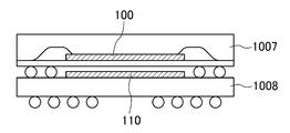
- the power supply device 100 can be realized by mounting the power supply device 100 on the PCB substrate 1007 and the SoC 110 under the PCB substrate 1008.
- FIG. 17 is a block diagram showing the configuration of the communication apparatus according to the eighth embodiment.
- the communication device is, for example, a mobile phone provided with the power supply device 100 and the SoC 110.
- the SoC 110 is a baseband LSI and an application LSI, respectively.
- the high frequency transmission / reception interface unit 1102 converts a signal received by the antenna into a power control signal Sctl1.
- the external input interface unit 1103 converts a signal input from a keyboard or the like into a power control signal Sctl2.
- voltage control is periodically performed by a timer in the baseband LSI, or voltage control according to Sctl1 is performed.
- the application LSI performs voltage control according to Sctl2. As described above, even in the communication device, the operation can be speeded up and the power consumption can be reduced.
- FIG. 18 is a block diagram showing the configuration of an AV apparatus according to a ninth embodiment.
- the AV device is, for example, an optical disk device provided with the power supply device 100 and the SoC 110.
- the SoC 110 is a media signal processing LSI that processes a signal read from an optical disk, and an error correction and servo processing LSI that performs error correction of the signal and servo control of an optical pickup.
- the tuner unit 1302 converts a signal received by the antenna into a power control signal Sctl1.
- the interface unit 1303 converts a signal input from a video input or the like into a power control signal Sctl2.
- the media signal processing LSI and the error correction / servo processing LSI perform voltage control according to Sctl1 and Sctl2, respectively. As described above, even in the AV apparatus such as the optical disk apparatus, the operation can be speeded up and the power consumption can be reduced.
- FIG. 19 is a block diagram showing the configuration of the AV apparatus according to the tenth embodiment.
- the AV device is, for example, a television receiver including the power supply device 100 and the SoC 110.
- the SoC 110 is an image / sound processing LSI that processes an image signal and an audio signal, and a display / sound source control LSI that controls devices such as a display screen and a speaker.
- the network interface unit 1502 converts a signal received by an antenna or the like into a power control signal Sctl1.
- the interface unit 1503 converts a signal input from a video input or the like into a power control signal Sctl2.
- voltage control is performed according to Sctl1 and Sctl2, respectively. As described above, even with an AV device such as a television receiver, the operation can be speeded up and the power consumption can be reduced.
- FIG. 20 is a block diagram showing the configuration of an imaging device according to the eleventh embodiment.
- the imaging device is, for example, a digital video camera provided with the power supply device 100 and the SoC 110.
- the SoC 110 is a signal processing LSI.
- a CCD (Charge Coupled Device) interface unit 1702 converts a signal acquired from the CCD into a power control signal Sctl.
- the interface unit 1703 converts a signal input from a video input or the like into Sctl.
- the signal processing LSI performs voltage control according to Sctl. As described above, even in the imaging device, the operation can be speeded up and the power consumption can be reduced.
- FIG. 21 is a block diagram showing configurations of an electronic control unit and a navigation apparatus according to a twelfth embodiment.
- the electronic control device and the navigation device include the power supply device 100 and the SoC 110, and are mounted on a mobile object such as a car.
- the SoC 110 is an engine / transmission control LSI and a navigation LSI, respectively.
- the interface unit 1902 converts a signal input from an accelerator or the like into a power control signal Sctl1.
- the navigation interface unit 1903 converts signals received by various antennas or the like into a power control signal Sctl2.
- voltage control is performed according to Sctl1 and Sctl2, respectively. As described above, it is possible to speed up the operation and reduce the power consumption of the electronic control device and the navigation device mounted on the vehicle.
- the semiconductor integrated circuit according to the present invention is useful for various electronic devices and the like for which fine voltage control and cost reduction are required because it is possible to perform voltage control with high resolution and high resolution while having a relatively simple configuration. It is.
Landscapes
- Engineering & Computer Science (AREA)
- Power Engineering (AREA)
- Physics & Mathematics (AREA)
- Electromagnetism (AREA)
- General Physics & Mathematics (AREA)
- Radar, Positioning & Navigation (AREA)
- Automation & Control Theory (AREA)
- Semiconductor Integrated Circuits (AREA)
- Continuous-Control Power Sources That Use Transistors (AREA)
- Control Of Voltage And Current In General (AREA)
- Dc-Dc Converters (AREA)
Abstract
アナログ制御信号(Vctl)に応じた大きさの電圧を生成する電源装置(100)から出力される電源電圧(Vsrc)で動作する半導体集積回路(110)は、電源電圧を受ける第1の端子(103)と、第1の端子に接続され、当該半導体集積回路内部の各部に電源電圧を分配する内部配線(114)と、アナログ制御信号を出力する第2の端子(104)とを備え、内部配線の電位に応じた大きさのアナログ制御信号を生成する。
Description
本発明は、電源制御システムに関し、特に、電源装置とその出力電圧で動作する半導体集積回路とを備えた電子機器における電源制御に関する。
図22に、非特許文献1に記載のアプリケーション回路を示す。この電源システムにおいては、電源IC2201の電源出力端子2202に、基板上で実装された、平滑コイル2203と平滑容量2204と抵抗分圧回路2205とが接続されている。さらに、抵抗分圧回路2205が接続されるノード2206にSoC(System-on-a-chip)2207の電源端子2208を接続することによりSoC2207に電源電圧を供給している。主にアナログ回路で構成された電源IC2201により、出力電圧が抵抗分圧回路2205により分圧された電圧VFBに応じた大きさの出力電圧が生成され、SoC2207は、この出力電圧を基準に電源電圧として受けて動作する。このタイプの電子機器では、抵抗分圧回路2205が固定抵抗で構成され分圧比が固定されるため、一度設定された出力電圧を動的に制御することはできない。また、抵抗分圧回路2205は電源IC2201直近に配置し、かつ、電源IC2201近傍のノード2206でしか電源電圧精度が保証されない。よって、電源IC2201からSoC2207までの配線による電源配線のインピーダンスや抵抗分圧回路2205の抵抗素子などの部品精度によりSoC2207の電源電圧は変動してしまう。その結果、SoC2207の性能は電源システムの電源電位の精度に大きく左右される。そこで、部品精度や電源配線インピーダンスに応じてSoC2207の電源電圧を動的かつ精度よく制御する技術が求められている。
図23に、非特許文献2に記載されているシステムの構成図を示す。この電源システムは、電源電圧を動的かつ精度よく制御できる電子機器の構成となっている。電源IC2301は、動的に電源電圧の制御を可能とするPM(パワーマネージメント)機能を有する。また、SoC2302は、回路遅延等の特性をモニタする性能モニタ回路(HPM)2303を有する。PM用の電源IC2301は、SoC2302から出力されたデジタルフィードバック信号2304を内部でデジタル処理するデジタル制御回路2305を有する。デジタル制御回路2305でデジタル処理された信号2306が内蔵DAC(D/Aコンバータ)回路でアナログ信号2307に変換され、出力電圧2308がSoC2302の要求性能に応じた電圧になるように制御される。SoC2302では、性能モニタ回路2303でモニタされた結果から、SoC2302の正常な回路動作に必要な電圧値が特定され、その電圧値がデジタルフィードバック信号2304としてPM用の電源IC2301に出力される。この電源システムでは、Vdd=0.6V~1.2Vくらいまでの範囲で出力電圧2308を制御することができる。
特許文献1では、電源回路(レギュレータ)とSoCの電力を最小とする電源電圧や基板電圧をデジタル信号処理演算し、電源電圧が所望の電源電圧値になるようレギュレータの抵抗分圧回路内の抵抗値を変化させて基準電圧を変え、システムの電力削減を実現する提案がされている。
LM5005 - High Voltage 2.5 Amp Buck Regulator. Datasheet. [online]. National Semiconductor, March 2006. [retrieved on 2011-04-28]. Retrieved from the Internet:<URL:http://www.alldatasheet.com/datasheet-pdf/pdf/180844/NSC/LM5005.html>
LP5552 - PWI 2.0 and PowerWise Technology Compliant Energy Management Unit. Datasheet. [online]. National Semiconductor, May 20,2008. [retrieved on 2011-04-28]. Retrieved from the Internet:<URL:http://www.alldatasheet.net/datasheet-pdf/pdf/239791/NSC/LP5552.html>
上記改良された電子機器では、SoC2302の要求性能に応じたデジタル信号のビット幅に応じた離散的な電圧制御しかできず、SoC2302に供給される電源電圧の可変ステップ幅は比較的大きくならざるを得ない。SoC2302の要求性能に応じたデジタル信号のビット数を拡張することで電圧制御のステップ幅が細かくなるが、電源IC2301に内蔵されている、デジタル処理をするロジック制御回路やそのデジタル信号をアナログ信号に変換するDAC回路等の規模が増大してしまい、コストが増大する。
かかる点に鑑みて、本発明は、比較的簡単な構成でありながらも動的で高分解能の電圧制御を可能とする電源制御システムを実現することを課題とする。
上記課題を解決するため本発明によって次のような解決手段を講じた。すなわち、アナログ制御信号に応じた大きさの電圧を生成する電源装置から出力される電源電圧で動作する半導体集積回路は、電源電圧を受ける第1の端子と、第1の端子に接続され、半導体集積回路内部の各部に電源電圧を分配する内部配線と、アナログ制御信号を出力する第2の端子とを備え、内部配線の電位に応じた大きさのアナログ制御信号を生成するものとする。
これによると、半導体集積回路の内部電圧に基づいて、アナログ制御信号により電源装置をフィードバック制御することにより、動的でかつ分解能が高い電圧制御を行うことができる。さらに、アナログ制御であるため回路構成が比較的簡単で済む。
例えば、上記半導体集積回路は、内部配線の電位を検出する電位モニタ回路と、電位モニタ回路が検出した電位に応じたアナログ制御信号を生成する電位制御回路とを備えていてもよい。
また、上記半導体集積回路は、それぞれ負荷が異なる複数の動作モードが切替可能な回路ブロックを備え、電位制御回路は、回路ブロックの動作モードの切り替わりに先立って切替後の回路ブロックの動作モードに応じた大きさのアナログ制御信号を生成してもよい。
これによると、例えば、回路ブロックが例えば高負荷状態になる場合に、それに先立って出力電圧を高くすることができるため、動作モードの切り替わり後に速やかに高負荷の回路ブロックを駆動することができる。
あるいは、上記半導体集積回路は、第1の端子が接続された第1のIO回路と、第2の端子が接続された第2のIO回路とを備え、第1および第2のIO回路は、互いに電気的に独立していてもよい。
例えば、上記半導体集積回路と、半導体集積回路から出力されたアナログ制御信号に応じた大きさの電源電圧を生成して半導体集積回路に供給する電源装置とを備えた電子機器が構成可能である。
好ましくは、上記電子機器において、半導体集積回路から電源装置にアナログ制御信号を伝送する配線はシールドされていてもよい。これによると、アナログ制御信号の耐ノイズ特性を向上することができる。
あるいは、3値以上の電圧値を持つ制御信号に応じた大きさの電圧を生成する電源装置から出力される電源電圧で動作する半導体集積回路は、電源電圧を受ける第1の端子と、第1の端子に接続され、半導体集積回路内部の各部に電源電圧を分配する内部配線と、制御信号を出力する第2の端子とを備え、内部配線の電位に応じた大きさの制御信号を生成してもよい。
本発明によると、比較的簡単な構成でありながらも動的でかつ高分解能の電圧制御を可能とする電源制御システムを実現することができる。
<第1の実施形態>
図1は、第1の実施形態に係る電子機器の構成を示すブロック図である。電子機器は、電源装置100およびSoC110を備えている。電源装置100は、SoC110からのフィードバック信号として、連続的に変化するアナログ制御信号Vctlを受け、Vctlに応じた大きさの電源電圧Vsrcを生成する。例えば、電源装置100は、汎用電源IC107およびPCB基板上に構成された平滑化回路109を有する。汎用電源IC107は、例えば降圧型スイッチングレギュレータICで構成することができる。なお、汎用電源IC107は、その他の電源ICであってもよい。汎用電源IC107では、Vctlに応じたデューティ比でスイッチ素子がスイッチング制御されて矩形波の電圧が生成される。平滑化回路109では、矩形波電圧が平滑化されることで、電源端子101から入力された例えば5V程度の入力電圧が1.2V程度に降圧されてVsrcが生成される。
図1は、第1の実施形態に係る電子機器の構成を示すブロック図である。電子機器は、電源装置100およびSoC110を備えている。電源装置100は、SoC110からのフィードバック信号として、連続的に変化するアナログ制御信号Vctlを受け、Vctlに応じた大きさの電源電圧Vsrcを生成する。例えば、電源装置100は、汎用電源IC107およびPCB基板上に構成された平滑化回路109を有する。汎用電源IC107は、例えば降圧型スイッチングレギュレータICで構成することができる。なお、汎用電源IC107は、その他の電源ICであってもよい。汎用電源IC107では、Vctlに応じたデューティ比でスイッチ素子がスイッチング制御されて矩形波の電圧が生成される。平滑化回路109では、矩形波電圧が平滑化されることで、電源端子101から入力された例えば5V程度の入力電圧が1.2V程度に降圧されてVsrcが生成される。
SoC110は、端子103でVsrcを受けて動作する。また、SoC110は、Vsrcを分配する電源線114の電位Vddに応じた大きさのVctlを生成し、端子104からVctlを出力する。例えば、SoC110は、Vddをモニタリングする電位モニタ回路112と、Vctlを生成する電位制御回路111と、Vddが供給されて動作する回路ブロック113とを有する。回路ブロック113は、単一の論理回路素子や複数の論理回路素子、あるいは、デバイス単体や複数のデバイスで構成することができる。
電位モニタ回路112は、Vddを検出して制御信号Ctlを生成する。電位制御回路111は、Ctlに応じた大きさのVctlを生成する。
図2は、従来の構成および本実施形態のそれぞれの電圧制御の一例を示す波形図である。回路ブロックに流れる動作電流Ioに応じて、従来と本実施形態とでどのような電圧制御が行われるかを模式的に示した波形図である。ここで、従来構成とは、SoC外部の電源電圧に基づいてフィードバック信号を生成する構成である。従来構成では、電流Ioが多い場合、時刻Tg1で、SoCの内部電圧Vddが低下する。一方、電流Ioが少ない場合、時刻Tg4でVddが上昇する。一般に、これらVddの変動幅を含めて電源ICの仕様では電圧精度として定義されている。
これに対して本実施形態では、電源線114に寄生するインピーダンスで決まるVddに応じてVctlが生成され、VctlによってVsrcおよびVddが制御される。時刻Tg1で電流Ioが増大してVddが低下すると、電位モニタ回路112は、Ctlの制御値を大きくする。これにより、Vddは時刻Tg2でTypical電圧値Vtypに回復する。さらに、電流Ioが多い状態が続くと、電位モニタ回路112は、Ctlの制御値をさらに大きくする。これにより、時刻Tg3以降Vddが上昇し、高負荷の回路ブロック113を駆動することができる。一方、時刻Tg4で電流Ioが減少すると、電位モニタ回路112は、Ctlの制御値を小さくする。これにより、Vddは時刻Tg5でVtypになる。その後、電流Ioが少ない状態が続くと、電位モニタ回路112は、Ctlの制御値をさらに小さくする。これにより、時刻Tg6でVddがVtypよりも低くなり、さらなる低電力化が実現される。
以上、本実施形態によると、SoC110の内部電圧Vddを含めたフィードバック補正が可能となり、Vsrcを動的に制御することができる。したがって、SoC110の動作の高速化や低電力化が実現可能となる。特に、従来の構成のようなデジタル制御の場合には、デジタル信号をクロック信号等でシリアル転送する必要があるため比較的消費電力が大きいが、本実施形態はアナログ制御であるため消費電力が比較的少なく、また、電圧制御の分解能を1mV単位などよりも小さくすることができ、非常に効率の良い電子機器を実現できる。さらに、比較的安価で汎用的な電源ICを用いることができるため、電子機器の低コスト化を図ることができる。また、VctlをSoC110で生成することで、プロセス微細化が困難な電源ICに電圧制御機能を搭載する従来の構成に比べて、電源装置100の回路面積を縮小することができる。
なお、電位モニタ回路112だけでなく例えば、動作エラー検知回路、ノイズマージン検知回路、温度検知回路、デバイス仕上がり検知回路、クロストークノイズ検知回路、ラッチアップ検知回路、信頼性劣化検知回路、EM耐性検知回路、遅延特性検知回路、耐圧検知回路などで各種特性をモニタリングし、その各種特性を電源装置100へのフィードバック電圧として帰還することも可能である。特に、電源電圧の感度の高い特性をモニタリングし、それを基に電源電圧を制御することにより、SoC110の性能を向上させることができる。
また、電位モニタ回路112は、電源線114の電位Vddよりも高い電源電圧VddHが供給されるMOS-FETを有していてもよい(図3参照)。このMOS-FETは、Vddが供給されるMOS-FETよりも高耐圧である。なお、VddHは、例えば1.8V,2.5V,3.3Vである。電位制御回路111には、電源電圧VddHが接続されていてもよい。また、電位制御回路111は、電源電圧VddHが供給されて動作するアナログ回路を含む。電位モニタ回路112および電位制御回路111のいずれか一方が電源電圧VddHに接続されていてもよい。これによると、Vddを高精度にモニタリングすることができ、高精度なVctlを生成することができる。
<第2の実施形態>
図4は、第2の実施形態に係る電子機器の構成を示すブロック図である。信号MODEは、回路ブロック113の負荷に応じた動作モードを示す信号である。回路ブロック113は、MODEに応じて、負荷が異なる複数の動作モードが切替可能に構成されている。電位制御回路111は、MODEに応じて回路ブロック113の動作モードが切り替わる前に、切替後の回路ブロック113の動作モードに応じた大きさのVctlを生成する。
図4は、第2の実施形態に係る電子機器の構成を示すブロック図である。信号MODEは、回路ブロック113の負荷に応じた動作モードを示す信号である。回路ブロック113は、MODEに応じて、負荷が異なる複数の動作モードが切替可能に構成されている。電位制御回路111は、MODEに応じて回路ブロック113の動作モードが切り替わる前に、切替後の回路ブロック113の動作モードに応じた大きさのVctlを生成する。
図5は、動作モードを加味して電圧制御される場合の波形図である。時刻Th2で回路ブロック113が高負荷となる高速動作モードに切り替わる場合、電位制御回路111は、時刻Th1で、高速動作モードに応じた大きさのVctlを生成する。これにより、Vsrcが上昇するためVddが上昇する。そして、時刻Th2で回路ブロック113が高速動作モードに切り替わって電流Ioが増加すると、Vddは低下するが、その後必要な電圧にすぐに回復する。なお、回路ブロック113が低負荷の動作モードの場合には、電位制御回路111は低負荷の動作モードに応じた大きさのVctlを生成すればよい。
以上、本実施形態によると、回路ブロック113の動作モードが切り替わる前に予めその動作モードに応じた電源電圧を生成することで、動作モードの変化に速やかに対応することができる。
<第3の実施形態>
図6は、第3の実施形態に係る電子機器の構成を示すブロック図である。SoC110は、メモリ回路619を有する。メモリ回路619は、電位モニタ回路112でモニタリングされたVddをデータ信号DATA2として記録する。また、メモリ回路619は、電位制御回路111で生成されたVctlをデータ信号DATA1として記録する。なお、メモリ回路619は、DATA1,DATA2のうちいずれか一方のみを記録してもよい。メモリ回路619に記録されたデータは、トリミング装置620によってトリミング等される。その後、メモリ回路619に記録されたデータは、電位モニタ回路112および電位制御回路111にそれぞれ再読み込みされ、電位モニタ回路112および電位制御回路111はそれぞれVctlおよびCtlを再生成する。
図6は、第3の実施形態に係る電子機器の構成を示すブロック図である。SoC110は、メモリ回路619を有する。メモリ回路619は、電位モニタ回路112でモニタリングされたVddをデータ信号DATA2として記録する。また、メモリ回路619は、電位制御回路111で生成されたVctlをデータ信号DATA1として記録する。なお、メモリ回路619は、DATA1,DATA2のうちいずれか一方のみを記録してもよい。メモリ回路619に記録されたデータは、トリミング装置620によってトリミング等される。その後、メモリ回路619に記録されたデータは、電位モニタ回路112および電位制御回路111にそれぞれ再読み込みされ、電位モニタ回路112および電位制御回路111はそれぞれVctlおよびCtlを再生成する。
以上、本実施形態によると、メモリ回路619に記録されたデータ信号をトリミング等することで、各信号の精度を向上させることができる。なお、メモリ回路619が不揮発性メモリの場合は、セット基板の搭載後においてもトリミング等が可能となる。また、メモリ回路619にチップID情報や回路ブロック113のデバイス仕上がり特性や温度情報などを記録してもよい。
<電位制御回路の具体例>
図7は、電位制御回路111の具体的な構成を示すブロック図である。電位制御回路111は、アナログバッファ回路を有し、例えばボルテージフォロワ回路で構成することができる。アナログバッファ回路は、電源電圧VddHが供給されるMOS-FETを有する。このMOS-FETは、電源電圧VDDが供給されるMOS-FETよりも高耐圧である。例えば、電位制御回路111は、可変分圧抵抗317とアナログバッファ回路318とで構成することができる。可変分圧抵抗317は、例えば、電位モニタ回路112の出力である信号Ctlを受けた抵抗可変制御回路319からの制御信号CTLR1,CTLR2に応じて抵抗値が変化し、電源電圧VddHを可変分圧する。アナログバッファ回路318は、分圧された電圧をVctlとして出力する。なお、抵抗可変制御回路319は、信号Ctlに応じて、制御信号CTLR1,CTLR2の制御値を変更するだけではなく、回路ブロック113の特性/性能に応じて、制御信号CTLR1,CTLR2の制御値を変更してもよい。なお、アナログバッファ回路318の入力側および出力側の間には、位相補償回路313またはゲイン補償回路313を搭載することが好ましい。また、高インピーダンスの配線には、電源電圧Vddやグランド電位等のシールド配線314を並走させることが好ましい。
図7は、電位制御回路111の具体的な構成を示すブロック図である。電位制御回路111は、アナログバッファ回路を有し、例えばボルテージフォロワ回路で構成することができる。アナログバッファ回路は、電源電圧VddHが供給されるMOS-FETを有する。このMOS-FETは、電源電圧VDDが供給されるMOS-FETよりも高耐圧である。例えば、電位制御回路111は、可変分圧抵抗317とアナログバッファ回路318とで構成することができる。可変分圧抵抗317は、例えば、電位モニタ回路112の出力である信号Ctlを受けた抵抗可変制御回路319からの制御信号CTLR1,CTLR2に応じて抵抗値が変化し、電源電圧VddHを可変分圧する。アナログバッファ回路318は、分圧された電圧をVctlとして出力する。なお、抵抗可変制御回路319は、信号Ctlに応じて、制御信号CTLR1,CTLR2の制御値を変更するだけではなく、回路ブロック113の特性/性能に応じて、制御信号CTLR1,CTLR2の制御値を変更してもよい。なお、アナログバッファ回路318の入力側および出力側の間には、位相補償回路313またはゲイン補償回路313を搭載することが好ましい。また、高インピーダンスの配線には、電源電圧Vddやグランド電位等のシールド配線314を並走させることが好ましい。
また、図8に示すように、図7におけるアナログバッファ回路318や位相/ゲイン補償回路313を省略し、可変分圧抵抗317の分圧ノードを直接Vctlとして出力する構成でもよい。これにより、アナログバッファ回路318の位相/ゲインを調整する必要がなくなり、回路面積を縮小することができる。
また、図9に示すように、位相補償回路313またはゲイン補償回路313をSoC110の外部に搭載してもよい。これらによると、分圧された電圧やアナログバッファ回路318の出力においてノイズの影響を低減することができるため、Vctlの精度を向上させることができる。
<第4の実施形態>
図10は、第4の実施形態に係る電子機器の構成を示すブロック図である。PCB基板109において、SoC110から電源装置100にVctlが伝送される配線には安定したグランド電位GND等のシールド配線825が並走する。
図10は、第4の実施形態に係る電子機器の構成を示すブロック図である。PCB基板109において、SoC110から電源装置100にVctlが伝送される配線には安定したグランド電位GND等のシールド配線825が並走する。
図11は、本実施形態に係るSoC110の構成を示すブロック図である。SoC110は、端子103に接続されるIO回路808と端子104に接続されるIO回路806とを備えている。IO回路806の電源804,805は、他のIO回路808等の電源と電気的に分離されている。また、SoC110において、Vctlが伝送される配線にはグランド電位等のシールド配線816が並走する。Vctlの伝送配線、電源線114およびグランド線115の間には可変容量素子807が接続される。
以上、本実施形態によると、Vctlの伝送配線は、周辺または外部からのノイズの混入が遮断されるため、安定かつ高精度なVctlを伝送することが可能となる。
<第5の実施形態>
図12は、第5の実施形態に係る電子機器の構成を示すブロック図である。SoC110は、回路ブロック113、電位モニタ回路112および電位制御回路111がそれぞれ例えば2つ搭載されたマルチブロックの構成である。
図12は、第5の実施形態に係る電子機器の構成を示すブロック図である。SoC110は、回路ブロック113、電位モニタ回路112および電位制御回路111がそれぞれ例えば2つ搭載されたマルチブロックの構成である。
具体的に、電位制御回路111は、Ctlに応じた大きさのアナログ信号であるフィードバック信号Fbを出力する。制御回路913は、MODEに応じたMfb(マルチ・フィードバック)信号を生成する。また、制御回路913は、MFB制御回路912に対して、いずれのFbをVctlとして電源装置100にフィードバックすべきかを指示する。MFB制御回路912は、FbおよびMfbを受け、Mfbに応じて2つのFbのうちいずれか一方を選択する。そして、MFB制御回路912は、選択したFbをVctlとして電源装置100にフィードバックする。これにより、マルチブロック構成の場合でも適正かつ安定した電圧制御が可能となる。
<第6の実施形態>
図13は、第6の実施形態に係る電子機器の構成を示すブロック図である。SoC110は、回路ブロック113、電位モニタ回路112および電位制御回路111がそれぞれ例えば2つ搭載されたマルチブロックの構成である。回路ブロック113にはそれぞれに対応する電源装置100からのVsrcに応じたVddが供給される。
図13は、第6の実施形態に係る電子機器の構成を示すブロック図である。SoC110は、回路ブロック113、電位モニタ回路112および電位制御回路111がそれぞれ例えば2つ搭載されたマルチブロックの構成である。回路ブロック113にはそれぞれに対応する電源装置100からのVsrcに応じたVddが供給される。
このようにSoC110内において複数の回路ブロック113が存在する場合、デバイスの仕上がりや回路ブロック113の機能などに応じて回路ブロック113の動作電圧が異なるため、それぞれの回路ブロック113の動作に必要な電圧を個別の電源装置100から供給することにより、各SoC110の性能をさらに向上させることができる。
<第7の実施形態>
図14は、第7の実施形態に係る電子機器の構成を示すブロック図である。判定回路2415は、同一のSoC110内のDATA1,DATA2を信号IFとして、他方のSoC110内の判定回路2415に出力する。判定回路2415は、同一のSoC110内のDATA1,DATA2および他方のSoC110から受けたIFを比較する。そして、比較した結果、いずれか一方のSoC110内の電位制御回路111で生成されたVctlをフィードバックすべき信号として出力制御回路2404に指示する。例えば、判定回路2415は、同一のSoC110内の電位制御回路111で生成されたVctlをフィードバックすべきと判定した場合に、同一のSoC110内の出力制御回路2404に対してそのVctlを出力するように指示する。
図14は、第7の実施形態に係る電子機器の構成を示すブロック図である。判定回路2415は、同一のSoC110内のDATA1,DATA2を信号IFとして、他方のSoC110内の判定回路2415に出力する。判定回路2415は、同一のSoC110内のDATA1,DATA2および他方のSoC110から受けたIFを比較する。そして、比較した結果、いずれか一方のSoC110内の電位制御回路111で生成されたVctlをフィードバックすべき信号として出力制御回路2404に指示する。例えば、判定回路2415は、同一のSoC110内の電位制御回路111で生成されたVctlをフィードバックすべきと判定した場合に、同一のSoC110内の出力制御回路2404に対してそのVctlを出力するように指示する。
出力制御回路2404は、判定回路2415に指示に従ってVctlを出力する。このような構成により、電源装置100の共有が可能となり、電子機器の省スペース化を図ることができる。なお、出力制御回路2404はいずれか一方のSoC110に搭載されていればよい。この場合、出力制御回路2404が搭載されたSoC110において、判定回路2415は、フィードバックすべきVctlを出力制御回路2404に指示すればよい。
また、いずれか一方のSoC110には、回路ブロック113のみが搭載されていてもよい。この場合、他方のSoC110からVctlを出力すればよい。
なお、上記各実施形態に係る電子機器ついて、図15に示すように、電源装置100とSoC110とその他のLSI1004,1005とチップコンデンサ1006をPCB基板1001に実装することでSIP(System In Package)化が可能である。また、図16に示すように、電源装置100をPCB基板上1007、SoC110をPCB基板1008下に実装することでPoP(Package On Package)化が可能である。これらSIPやPoPのように電源装置100およびSoC110をパッケージに統合することにより、各電源配線や信号配線に寄生するインピーダンス設計が容易となる。
<第8の実施形態>
図17は、第8の実施形態に係る通信装置の構成を示すブロック図である。通信装置は、電源装置100およびSoC110を備えた例えば携帯電話である。SoC110は、それぞれベースバンドLSIおよびアプリケーションLSIである。高周波送受信インターフェース部1102は、アンテナで受信した信号を電源制御信号Sctl1に変換する。外部入力インターフェース部1103は、キーボード等から入力された信号を電源制御信号Sctl2に変換する。ベースバンドLSIでは、ベースバンドLSI内のタイマーにより定期的に電圧制御が行われたり、Sctl1に応じた電圧制御が行われる。アプリケーションLSIでは、Sctl2に応じた電圧制御が行われる。このように、通信装置でも動作の高速化や消費電力の低減を図ることができる。
図17は、第8の実施形態に係る通信装置の構成を示すブロック図である。通信装置は、電源装置100およびSoC110を備えた例えば携帯電話である。SoC110は、それぞれベースバンドLSIおよびアプリケーションLSIである。高周波送受信インターフェース部1102は、アンテナで受信した信号を電源制御信号Sctl1に変換する。外部入力インターフェース部1103は、キーボード等から入力された信号を電源制御信号Sctl2に変換する。ベースバンドLSIでは、ベースバンドLSI内のタイマーにより定期的に電圧制御が行われたり、Sctl1に応じた電圧制御が行われる。アプリケーションLSIでは、Sctl2に応じた電圧制御が行われる。このように、通信装置でも動作の高速化や消費電力の低減を図ることができる。
<第9の実施形態>
図18は、第9の実施形態に係るAV機器の構成を示すブロック図である。AV機器は、電源装置100およびSoC110を備えた例えば光ディスク装置である。SoC110は、それぞれ光ディスクから読み取った信号を処理するメディア信号処理LSIおよびその信号の誤り訂正や光ピックアップのサーボ制御を行う誤り訂正・サーボ処理LSIである。
図18は、第9の実施形態に係るAV機器の構成を示すブロック図である。AV機器は、電源装置100およびSoC110を備えた例えば光ディスク装置である。SoC110は、それぞれ光ディスクから読み取った信号を処理するメディア信号処理LSIおよびその信号の誤り訂正や光ピックアップのサーボ制御を行う誤り訂正・サーボ処理LSIである。
チューナー部1302は、アンテナで受信した信号を電源制御信号Sctl1に変換する。インターフェース部1303は、ビデオ入力等から入力された信号を電源制御信号Sctl2に変換する。メディア信号処理LSIおよび誤り訂正・サーボ処理LSIでは、それぞれSctl1,Sctl2に応じた電圧制御が行われる。このように、光ディスク装置のようなAV機器でも動作の高速化や消費電力の低減を図ることができる。
<第10の実施形態>
図19は、第10の実施形態に係るAV機器の構成を示すブロック図である。AV機器は例えば、電源装置100およびSoC110を備えたテレビジョン受像機である。SoC110は、それぞれ画像信号や音声信号を処理する画像・音声処理LSIおよび表示画面やスピーカなどのデバイスを制御するディスプレイ・音源制御LSIである。
図19は、第10の実施形態に係るAV機器の構成を示すブロック図である。AV機器は例えば、電源装置100およびSoC110を備えたテレビジョン受像機である。SoC110は、それぞれ画像信号や音声信号を処理する画像・音声処理LSIおよび表示画面やスピーカなどのデバイスを制御するディスプレイ・音源制御LSIである。
ネットワークインターフェース部1502は、アンテナ等で受信した信号を電源制御信号Sctl1に変換する。インターフェース部1503は、ビデオ入力等から入力された信号を電源制御信号Sctl2に変換する。画像・音声処理LSIおよびディスプレイ・音源制御LSIでは、それぞれSctl1,Sctl2に応じた電圧制御が行われる。このように、テレビジョン受像機のようなAV機器でも動作の高速化や消費電力の低減を図ることができる。
<第11の実施形態>
図20は、第11の実施形態に係る撮像装置の構成を示すブロック図である。撮像装置は例えば、電源装置100およびSoC110を備えたデジタルビデオカメラである。SoC110は、信号処理LSIである。
図20は、第11の実施形態に係る撮像装置の構成を示すブロック図である。撮像装置は例えば、電源装置100およびSoC110を備えたデジタルビデオカメラである。SoC110は、信号処理LSIである。
CCD(Charge Coupled Device)インターフェース部1702は、CCDから取得した信号を電源制御信号Sctlに変換する。インターフェース部1703は、ビデオ入力等から入力された信号をSctlに変換する。信号処理LSIでは、Sctlに応じた電圧制御が行われる。このように、撮像装置でも動作の高速化や消費電力の低減を図ることができる。
<第12の実施形態>
図21は、第12の実施形態に係る電子制御装置およびナビゲーション装置の構成を示すブロック図である。電子制御装置およびナビゲーション装置は、電源装置100およびSoC110を備え、例えば自動車等の移動体に搭載されている。SoC110は、それぞれエンジン・トランスミッション制御LSIおよびナビゲーション用LSIである。
図21は、第12の実施形態に係る電子制御装置およびナビゲーション装置の構成を示すブロック図である。電子制御装置およびナビゲーション装置は、電源装置100およびSoC110を備え、例えば自動車等の移動体に搭載されている。SoC110は、それぞれエンジン・トランスミッション制御LSIおよびナビゲーション用LSIである。
インターフェース部1902は、アクセル等から入力された信号を電源制御信号Sctl1に変換する。ナビゲーションインターフェース部1903は、各種アンテナ等で受信した信号を電源制御信号Sctl2に変換する。エンジン・トランスミッション制御LSIおよびナビゲーション用LSIでは、それぞれSctl1,Sctl2に応じた電圧制御が行われる。このように、自動車に搭載された電子制御装置やナビゲーション装置についても、動作の高速化や消費電力の低減を図ることができる。
本発明に係る半導体集積回路は、比較的簡単な構成でありながらも動的でかつ高分解能の電圧制御が可能であるため、細かな電圧制御や低コスト化が求められる各種電子機器等に有用である。
100 電源装置
103 端子(第1の端子)
104 端子(第2の端子)
107 汎用電源IC(スイッチング電源回路)
109 平滑化回路
110 SoC(半導体集積回路)
111 電位モニタ回路
112 電位制御回路
113 回路ブロック
114 内部配線
313 位相補償回路、ゲイン補償回路
619 メモリ回路
806 IO回路(第2のIO回路)
808 IO回路(第1のIO回路)
1102 高周波送受信インターフェース部
1103 外部入力インターフェース部
1302 チューナー部
1303 外部入力インターフェース部
1502 ネットワークインターフェース部
1503 外部入力インターフェース部
1702 CCDインターフェース部
1703 外部入力インターフェース部
1903 ナビゲーションインターフェース部
Vctl アナログ制御信号
Vsrc 電源電圧
VddH 電源電圧
Claims (20)
- アナログ制御信号に応じた大きさの電圧を生成する電源装置から出力される電源電圧で動作する半導体集積回路であって、
前記電源電圧を受ける第1の端子と、
前記第1の端子に接続され、当該半導体集積回路内部の各部に前記電源電圧を分配する内部配線と、
前記アナログ制御信号を出力する第2の端子とを備え、
前記内部配線の電位に応じた大きさの前記アナログ制御信号を生成する
ことを特徴とする半導体集積回路。 - 請求項1の半導体集積回路において、
前記内部配線の電位を検出する電位モニタ回路と、
前記電位モニタ回路が検出した電位に応じた大きさの前記アナログ制御信号を生成する電位制御回路とを備えている
ことを特徴とする半導体集積回路。 - 請求項2の半導体集積回路において、
それぞれ負荷が異なる複数の動作モードが切替可能な回路ブロックを備え、
前記電位制御回路は、前記回路ブロックの動作モードの切り替わりに先立って切替後の前記回路ブロックの動作モードに応じた大きさの前記アナログ制御信号を生成する
ことを特徴とする半導体集積回路。 - 請求項2の半導体集積回路において、
前記電位モニタ回路は、前記内部配線の電位よりも高い電源電圧が供給されるMOS-FETを有するものであり、
前記MOS-FETは、前記内部配線の電位が供給されるMOS-FETよりも高耐圧である
ことを特徴とする半導体集積回路。 - 請求項2の半導体集積回路において、
前記電位制御回路は、前記内部配線の電位よりも高い電源電圧に接続される
ことを特徴とする半導体集積回路。 - 請求項2の半導体集積回路において、
前記電位制御回路は、アナログバッファ回路を有し、前記アナログバッファ回路を介して前記アナログ制御信号を出力する
ことを特徴とする半導体集積回路。 - 請求項6の半導体集積回路において、
前記アナログバッファ回路は、前記内部配線の電位よりも高い電源電圧が供給されるMOS-FETを有するものであり、
前記MOS-FETは、前記内部配線の電位が供給されるMOS-FETよりも高耐圧である
ことを特徴とする半導体集積回路。 - 請求項7の半導体集積回路において、
前記アナログバッファ回路の入力側および出力側の間には、位相補償回路またはゲイン補償回路が接続されている
ことを特徴とする半導体集積回路。 - 請求項2の半導体集積回路において、
前記電位モニタ回路が検出した電位をデータ化して記録するメモリ回路を備えている
ことを特徴とする半導体集積回路。 - 請求項2の半導体集積回路において、
前記アナログ制御信号をデータ化して記録するメモリ回路を備えている
ことを特徴とする半導体集積回路。 - 請求項1の半導体集積回路において、
前記第1の端子が接続された第1のIO回路と、
前記第2の端子が接続された第2のIO回路とを備え、
前記第1および第2のIO回路は、互いに電気的に独立している
ことを特徴とする半導体集積回路。 - 請求項1の半導体集積回路と、
前記半導体集積回路から出力されたアナログ制御信号に応じた大きさの電源電圧を生成して前記半導体集積回路に供給する電源装置とを備えている
ことを特徴とする電子機器。 - 請求項12の電子機器において、
前記電源装置は、
前記アナログ制御信号に応じたデューティ比でスイッチ素子をスイッチング制御して入力電圧を変圧するスイッチング電源回路と、
前記スイッチング電源回路から出力される矩形波電圧を平滑化して前記電源電圧を生成する平滑化回路とを有する
ことを特徴とする電子機器。 - 請求項12の電子機器において、
前記半導体集積回路から前記電源装置に前記アナログ制御信号を伝送する配線はシールドされている
ことを特徴とする電子機器。 - 請求項1の半導体集積回路と、
前記半導体集積回路から出力されたアナログ制御信号に応じた大きさの電源電圧を生成して前記半導体集積回路に供給する電源装置と、
前記半導体集積回路に接続された高周波送受信インターフェース部と、
前記半導体集積回路に接続された外部入力インターフェース部とを備えている
ことを特徴とする通信装置。 - 請求項1の半導体集積回路と、
前記半導体集積回路から出力されたアナログ制御信号に応じた大きさの電源電圧を生成して前記半導体集積回路に供給する電源装置と、
前記半導体集積回路に接続されたチューナー部と、
前記半導体集積回路に接続されたインターフェース部とを備えている
ことを特徴とするAV機器。 - 請求項1の半導体集積回路と、
前記半導体集積回路から出力されたアナログ制御信号に応じた大きさの電源電圧を生成して前記半導体集積回路に供給する電源装置と、
前記半導体集積回路に接続されたネットワークインターフェース部と、
前記半導体集積回路に接続された外部入力インターフェース部とを備えている
ことを特徴とするAV機器。 - 請求項1の半導体集積回路と、
前記半導体集積回路から出力されたアナログ制御信号に応じた大きさの電源電圧を生成して前記半導体集積回路に供給する電源装置と、
前記半導体集積回路に接続されたCCDインターフェース部と、
前記半導体集積回路に接続された外部入力インターフェース部とを備えている
ことを特徴とする撮像装置。 - 請求項1の半導体集積回路と、
前記半導体集積回路から出力されたアナログ制御信号に応じた大きさの電源電圧を生成して前記半導体集積回路に供給する電源装置と、
前記半導体集積回路に接続されたナビゲーションインターフェース部とを備えている
ことを特徴とするナビゲーション装置。 - 3値以上の電圧値を持つ制御信号に応じた大きさの電圧を生成する電源装置から出力される電源電圧で動作する半導体集積回路であって、
前記電源電圧を受ける第1の端子と、
前記第1の端子に接続され、当該半導体集積回路内部の各部に前記電源電圧を分配する内部配線と、
前記制御信号を出力する第2の端子とを備え、
前記内部配線の電位に応じた大きさの前記制御信号を生成する
ことを特徴とする半導体集積回路。
Priority Applications (2)
| Application Number | Priority Date | Filing Date | Title |
|---|---|---|---|
| JP2012523510A JPWO2012004935A1 (ja) | 2010-07-08 | 2011-06-10 | 半導体集積回路およびそれを備えた電子機器 |
| US13/732,991 US8774255B2 (en) | 2010-07-08 | 2013-01-02 | Semiconductor integrated circuit and electronic apparatus provided with same |
Applications Claiming Priority (2)
| Application Number | Priority Date | Filing Date | Title |
|---|---|---|---|
| JP2010155534 | 2010-07-08 | ||
| JP2010-155534 | 2010-07-08 |
Related Child Applications (1)
| Application Number | Title | Priority Date | Filing Date |
|---|---|---|---|
| US13/732,991 Continuation US8774255B2 (en) | 2010-07-08 | 2013-01-02 | Semiconductor integrated circuit and electronic apparatus provided with same |
Publications (1)
| Publication Number | Publication Date |
|---|---|
| WO2012004935A1 true WO2012004935A1 (ja) | 2012-01-12 |
Family
ID=45440931
Family Applications (1)
| Application Number | Title | Priority Date | Filing Date |
|---|---|---|---|
| PCT/JP2011/003289 WO2012004935A1 (ja) | 2010-07-08 | 2011-06-10 | 半導体集積回路およびそれを備えた電子機器 |
Country Status (3)
| Country | Link |
|---|---|
| US (1) | US8774255B2 (ja) |
| JP (1) | JPWO2012004935A1 (ja) |
| WO (1) | WO2012004935A1 (ja) |
Cited By (1)
| Publication number | Priority date | Publication date | Assignee | Title |
|---|---|---|---|---|
| WO2015029293A1 (ja) * | 2013-08-27 | 2015-03-05 | パナソニック株式会社 | 半導体集積回路および複数の半導体集積回路を備えた電源制御システム |
Families Citing this family (1)
| Publication number | Priority date | Publication date | Assignee | Title |
|---|---|---|---|---|
| CN106020170B (zh) * | 2016-07-07 | 2019-03-15 | 工业和信息化部电子第五研究所 | SoC健康监测的方法、装置及系统 |
Citations (3)
| Publication number | Priority date | Publication date | Assignee | Title |
|---|---|---|---|---|
| JP2004228104A (ja) * | 2003-01-17 | 2004-08-12 | Matsushita Electric Ind Co Ltd | 半導体集積回路 |
| JP2007201455A (ja) * | 2005-12-28 | 2007-08-09 | Matsushita Electric Ind Co Ltd | 半導体集積回路装置 |
| JP2009016776A (ja) * | 2007-06-08 | 2009-01-22 | Renesas Technology Corp | 半導体集積回路 |
Family Cites Families (2)
| Publication number | Priority date | Publication date | Assignee | Title |
|---|---|---|---|---|
| US20090033155A1 (en) * | 2007-06-08 | 2009-02-05 | Renesas Technology Corp. | Semiconductor integrated circuits |
| US9305590B2 (en) * | 2007-10-16 | 2016-04-05 | Seagate Technology Llc | Prevent data storage device circuitry swap |
-
2011
- 2011-06-10 JP JP2012523510A patent/JPWO2012004935A1/ja not_active Withdrawn
- 2011-06-10 WO PCT/JP2011/003289 patent/WO2012004935A1/ja active Application Filing
-
2013
- 2013-01-02 US US13/732,991 patent/US8774255B2/en active Active
Patent Citations (3)
| Publication number | Priority date | Publication date | Assignee | Title |
|---|---|---|---|---|
| JP2004228104A (ja) * | 2003-01-17 | 2004-08-12 | Matsushita Electric Ind Co Ltd | 半導体集積回路 |
| JP2007201455A (ja) * | 2005-12-28 | 2007-08-09 | Matsushita Electric Ind Co Ltd | 半導体集積回路装置 |
| JP2009016776A (ja) * | 2007-06-08 | 2009-01-22 | Renesas Technology Corp | 半導体集積回路 |
Cited By (4)
| Publication number | Priority date | Publication date | Assignee | Title |
|---|---|---|---|---|
| WO2015029293A1 (ja) * | 2013-08-27 | 2015-03-05 | パナソニック株式会社 | 半導体集積回路および複数の半導体集積回路を備えた電源制御システム |
| JPWO2015029293A1 (ja) * | 2013-08-27 | 2017-03-02 | 株式会社ソシオネクスト | 半導体集積回路および複数の半導体集積回路を備えた電源制御システム |
| US9766640B2 (en) | 2013-08-27 | 2017-09-19 | Socionext Inc. | Semiconductor integrated circuit and power supply control system provided with a plurality of semiconductor integrated circuits |
| US9880572B2 (en) | 2013-08-27 | 2018-01-30 | Socionext Inc. | Semiconductor integrated circuit and power supply control system provided with a plurality of semiconductor integrated circuits |
Also Published As
| Publication number | Publication date |
|---|---|
| US20130136162A1 (en) | 2013-05-30 |
| US8774255B2 (en) | 2014-07-08 |
| JPWO2012004935A1 (ja) | 2013-09-02 |
Similar Documents
| Publication | Publication Date | Title |
|---|---|---|
| US11193961B2 (en) | Current balancing, current sensor, and phase balancing apparatus and method for a voltage regulator | |
| US10990146B2 (en) | Digital synthesizable low dropout regulator with adaptive gain | |
| US10673335B2 (en) | Reconfigurable power regulator | |
| KR102247952B1 (ko) | 하이브리드 전압 조정기에서의 피드백 제어 | |
| US7170273B2 (en) | Power-supply device and hard disk drive using same | |
| TWI554013B (zh) | 用於操作電壓調整器之方法、設備及系統 | |
| TWI661669B (zh) | 多級放大器 | |
| US6522160B1 (en) | Input buffer with automatic switching point adjustment circuitry, and synchronous DRAM device including same | |
| US20070242557A1 (en) | Control circuit of power supply unit, power supply unit and control method thereof | |
| US9948186B2 (en) | Master-slave digital voltage regulators | |
| US10411599B1 (en) | Boost and LDO hybrid converter with dual-loop control | |
| EP2775481B1 (en) | Apparatus and method for reducing sampling circuit timing mismatch | |
| US20170359492A1 (en) | Image Sensors Including Ripple Voltage Compensation | |
| US20180059156A1 (en) | Apparatus and method for calibrating high speed serial receiver analog front end and phase detector | |
| US20150346247A1 (en) | Digital current sensor for on-die switching voltage regulator | |
| WO2012004935A1 (ja) | 半導体集積回路およびそれを備えた電子機器 | |
| CN116711197A (zh) | 用于输入电流调节的方法以及具有输入电压前馈和输出负载前馈的有源功率滤波器 | |
| US20070127169A1 (en) | Integrated circuit with configurable bypass capacitance | |
| US20070069762A1 (en) | Input buffer with automatic switching point adjustment circuitry, and synchronous DRAM device including same | |
| US9638720B2 (en) | Low power current sensor | |
| US11082050B2 (en) | Clock distribution circuit using adjustable phase control and voltage converter including the same | |
| US11139820B1 (en) | Efficient digital gain implementation in digital microphones | |
| WO2014207969A1 (ja) | レギュレータ回路、電圧安定化回路及び半導体装置 |
Legal Events
| Date | Code | Title | Description |
|---|---|---|---|
| 121 | Ep: the epo has been informed by wipo that ep was designated in this application |
Ref document number: 11803277 Country of ref document: EP Kind code of ref document: A1 |
|
| WWE | Wipo information: entry into national phase |
Ref document number: 2012523510 Country of ref document: JP |
|
| NENP | Non-entry into the national phase |
Ref country code: DE |
|
| 122 | Ep: pct application non-entry in european phase |
Ref document number: 11803277 Country of ref document: EP Kind code of ref document: A1 |