WO2012002271A1 - 太陽電池セル、配線付き太陽電池セル、太陽電池モジュールおよび配線付き太陽電池セルの製造方法 - Google Patents
太陽電池セル、配線付き太陽電池セル、太陽電池モジュールおよび配線付き太陽電池セルの製造方法 Download PDFInfo
- Publication number
- WO2012002271A1 WO2012002271A1 PCT/JP2011/064526 JP2011064526W WO2012002271A1 WO 2012002271 A1 WO2012002271 A1 WO 2012002271A1 JP 2011064526 W JP2011064526 W JP 2011064526W WO 2012002271 A1 WO2012002271 A1 WO 2012002271A1
- Authority
- WO
- WIPO (PCT)
- Prior art keywords
- electrode
- solar cell
- type
- wiring
- wiring member
- Prior art date
- Legal status (The legal status is an assumption and is not a legal conclusion. Google has not performed a legal analysis and makes no representation as to the accuracy of the status listed.)
- Ceased
Links
Images





Classifications
-
- H—ELECTRICITY
- H10—SEMICONDUCTOR DEVICES; ELECTRIC SOLID-STATE DEVICES NOT OTHERWISE PROVIDED FOR
- H10F—INORGANIC SEMICONDUCTOR DEVICES SENSITIVE TO INFRARED RADIATION, LIGHT, ELECTROMAGNETIC RADIATION OF SHORTER WAVELENGTH OR CORPUSCULAR RADIATION
- H10F77/00—Constructional details of devices covered by this subclass
- H10F77/20—Electrodes
- H10F77/206—Electrodes for devices having potential barriers
- H10F77/211—Electrodes for devices having potential barriers for photovoltaic cells
- H10F77/219—Arrangements for electrodes of back-contact photovoltaic cells
-
- H—ELECTRICITY
- H10—SEMICONDUCTOR DEVICES; ELECTRIC SOLID-STATE DEVICES NOT OTHERWISE PROVIDED FOR
- H10F—INORGANIC SEMICONDUCTOR DEVICES SENSITIVE TO INFRARED RADIATION, LIGHT, ELECTROMAGNETIC RADIATION OF SHORTER WAVELENGTH OR CORPUSCULAR RADIATION
- H10F10/00—Individual photovoltaic cells, e.g. solar cells
- H10F10/10—Individual photovoltaic cells, e.g. solar cells having potential barriers
- H10F10/14—Photovoltaic cells having only PN homojunction potential barriers
- H10F10/146—Back-junction photovoltaic cells, e.g. having interdigitated base-emitter regions on the back side
-
- H—ELECTRICITY
- H10—SEMICONDUCTOR DEVICES; ELECTRIC SOLID-STATE DEVICES NOT OTHERWISE PROVIDED FOR
- H10F—INORGANIC SEMICONDUCTOR DEVICES SENSITIVE TO INFRARED RADIATION, LIGHT, ELECTROMAGNETIC RADIATION OF SHORTER WAVELENGTH OR CORPUSCULAR RADIATION
- H10F19/00—Integrated devices, or assemblies of multiple devices, comprising at least one photovoltaic cell covered by group H10F10/00, e.g. photovoltaic modules
- H10F19/80—Encapsulations or containers for integrated devices, or assemblies of multiple devices, having photovoltaic cells
-
- H—ELECTRICITY
- H10—SEMICONDUCTOR DEVICES; ELECTRIC SOLID-STATE DEVICES NOT OTHERWISE PROVIDED FOR
- H10F—INORGANIC SEMICONDUCTOR DEVICES SENSITIVE TO INFRARED RADIATION, LIGHT, ELECTROMAGNETIC RADIATION OF SHORTER WAVELENGTH OR CORPUSCULAR RADIATION
- H10F19/00—Integrated devices, or assemblies of multiple devices, comprising at least one photovoltaic cell covered by group H10F10/00, e.g. photovoltaic modules
- H10F19/90—Structures for connecting between photovoltaic cells, e.g. interconnections or insulating spacers
-
- H—ELECTRICITY
- H10—SEMICONDUCTOR DEVICES; ELECTRIC SOLID-STATE DEVICES NOT OTHERWISE PROVIDED FOR
- H10F—INORGANIC SEMICONDUCTOR DEVICES SENSITIVE TO INFRARED RADIATION, LIGHT, ELECTROMAGNETIC RADIATION OF SHORTER WAVELENGTH OR CORPUSCULAR RADIATION
- H10F19/00—Integrated devices, or assemblies of multiple devices, comprising at least one photovoltaic cell covered by group H10F10/00, e.g. photovoltaic modules
- H10F19/90—Structures for connecting between photovoltaic cells, e.g. interconnections or insulating spacers
- H10F19/902—Structures for connecting between photovoltaic cells, e.g. interconnections or insulating spacers for series or parallel connection of photovoltaic cells
- H10F19/908—Structures for connecting between photovoltaic cells, e.g. interconnections or insulating spacers for series or parallel connection of photovoltaic cells for back-contact photovoltaic cells
-
- H—ELECTRICITY
- H10—SEMICONDUCTOR DEVICES; ELECTRIC SOLID-STATE DEVICES NOT OTHERWISE PROVIDED FOR
- H10F—INORGANIC SEMICONDUCTOR DEVICES SENSITIVE TO INFRARED RADIATION, LIGHT, ELECTROMAGNETIC RADIATION OF SHORTER WAVELENGTH OR CORPUSCULAR RADIATION
- H10F71/00—Manufacture or treatment of devices covered by this subclass
- H10F71/137—Batch treatment of the devices
-
- H—ELECTRICITY
- H10—SEMICONDUCTOR DEVICES; ELECTRIC SOLID-STATE DEVICES NOT OTHERWISE PROVIDED FOR
- H10F—INORGANIC SEMICONDUCTOR DEVICES SENSITIVE TO INFRARED RADIATION, LIGHT, ELECTROMAGNETIC RADIATION OF SHORTER WAVELENGTH OR CORPUSCULAR RADIATION
- H10F77/00—Constructional details of devices covered by this subclass
- H10F77/20—Electrodes
- H10F77/206—Electrodes for devices having potential barriers
- H10F77/211—Electrodes for devices having potential barriers for photovoltaic cells
-
- H—ELECTRICITY
- H10—SEMICONDUCTOR DEVICES; ELECTRIC SOLID-STATE DEVICES NOT OTHERWISE PROVIDED FOR
- H10F—INORGANIC SEMICONDUCTOR DEVICES SENSITIVE TO INFRARED RADIATION, LIGHT, ELECTROMAGNETIC RADIATION OF SHORTER WAVELENGTH OR CORPUSCULAR RADIATION
- H10F77/00—Constructional details of devices covered by this subclass
- H10F77/30—Coatings
- H10F77/306—Coatings for devices having potential barriers
- H10F77/311—Coatings for devices having potential barriers for photovoltaic cells
-
- Y—GENERAL TAGGING OF NEW TECHNOLOGICAL DEVELOPMENTS; GENERAL TAGGING OF CROSS-SECTIONAL TECHNOLOGIES SPANNING OVER SEVERAL SECTIONS OF THE IPC; TECHNICAL SUBJECTS COVERED BY FORMER USPC CROSS-REFERENCE ART COLLECTIONS [XRACs] AND DIGESTS
- Y02—TECHNOLOGIES OR APPLICATIONS FOR MITIGATION OR ADAPTATION AGAINST CLIMATE CHANGE
- Y02E—REDUCTION OF GREENHOUSE GAS [GHG] EMISSIONS, RELATED TO ENERGY GENERATION, TRANSMISSION OR DISTRIBUTION
- Y02E10/00—Energy generation through renewable energy sources
- Y02E10/50—Photovoltaic [PV] energy
- Y02E10/547—Monocrystalline silicon PV cells
Definitions
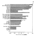
- a metal material is usually used for the electrode of the back electrode type solar cell and the wiring of the wiring sheet, but the metal material has an ion migration property that a metal material ionized by an electric field is deposited along the electric field direction. is doing.
- the ease with which this ion migration occurs depends on the type of metal material and the electric field strength of the electric field when the ambient temperature and humidity are the same.
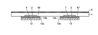
- FIG. 1 typical sectional drawing of the photovoltaic cell of Embodiment 1 which is an example of the photovoltaic cell of this invention is shown.
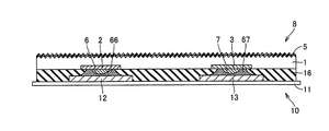
- the n-type electrode 6 and the p-type electrode 7 having different polarities are provided on one surface side of the substrate 1.
- Each is a back electrode type solar cell provided.
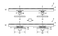
- the covering layer 66 only needs to cover at least part of the surface of the n-type electrode 6, and the covering layer 67 only needs to cover at least part of the surface of the p-type electrode 7. From the viewpoint of stably suppressing the resulting deterioration of the characteristics of the solar battery cell, the covering layer 66 covers the entire surface of the n-type electrode 6 and the covering layer 67 covers the entire surface of the p-type electrode 7. It is preferable.
- an n-type impurity diffusion region 2 and a p-type impurity diffusion region 3 are formed on the back surface of the substrate 1, respectively.
- the n-type impurity diffusion region 2 can be formed by, for example, a method such as vapor phase diffusion using a gas containing n-type impurities or coating diffusion in which a heat treatment is applied after applying a paste containing n-type impurities.
- the p-type impurity diffusion region 3 can be formed, for example, by a method such as vapor phase diffusion using a gas containing p-type impurities or coating diffusion in which a heat treatment is applied after applying a paste containing p-type impurities.
- the resist 42 is completely removed from the surface of the n-type wiring member 12 and the surface of the p-type wiring member 13.
- the wiring sheet 10 in which the n-type wiring member 12 and the p-type wiring member 13 are formed on the insulating substrate 11 is produced.
- a member, a wiring member for electrically connecting the plurality of p-type wiring members 13, a wiring member for electrically connecting the plurality of solar cells 8, and the like may be formed.
Landscapes
- Photovoltaic Devices (AREA)
- Manufacturing Of Printed Wiring (AREA)
- Engineering & Computer Science (AREA)
- Manufacturing & Machinery (AREA)
- Life Sciences & Earth Sciences (AREA)
- Sustainable Development (AREA)
- Sustainable Energy (AREA)
Abstract
Description
図1に、本発明の太陽電池セルの一例である実施の形態1の太陽電池セルの模式的な断面図を示す。ここで、実施の形態1の太陽電池セルは、図1に示すように、基板1の一方の面側に互いに異なる極性(負極、正極)となるn型用電極6およびp型用電極7がそれぞれ設けられた裏面電極型太陽電池セルである。
実施の形態2の配線付き太陽電池セルは、実施の形態1の太陽電池セル8の複数が配線部材によって電気的に接続されていることを特徴としている。
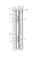
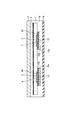
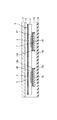
図11に本発明の配線付き太陽電池セルのさらに他の一例である実施の形態3の配線付き太陽電池セルの模式的な断面図を示し、図12に本発明の太陽電池モジュールのさらに他の一例である実施の形態3の太陽電池モジュールの模式的な断面図を示す。
Claims (13)
- 基板(1)と、
前記基板(1)の一方の面側に設けられた第1の電極(6,7)と、
前記第1の電極(6,7)の表面を覆う第1の被覆層(66,67)と、を備え、
前記第1の被覆層(66,67)は、前記第1の電極(6,7)を構成する金属材料よりもイオンマイグレーションが起こり難い材料からなる、太陽電池セル(8)。 - 前記第1の被覆層(66,67)が導電性材料からなる、請求項1に記載の太陽電池セル(8)。
- 前記太陽電池セル(8)は裏面電極型太陽電池セルである、請求項1または2に記載の太陽電池セル(8)。
- 前記基板(1)の一方の面側に設けられた第2の電極(6,7)と、
前記第2の電極(6,7)の表面を覆う第2の被覆層(66,67)と、をさらに備え、
前記第2の電極(6,7)は前記第1の電極(6,7)とは異なる極性の電極であり、
前記第2の被覆層(66,67)は、前記第2の電極(6,7)を構成する金属材料よりもイオンマイグレーションが起こり難い材料からなる、請求項1から3のいずれかに記載の太陽電池セル(8)。 - 前記第2の被覆層(66,67)が導電性材料からなる、請求項4に記載の太陽電池セル(8)。
- 基板(1)と、
前記基板(1)の一方の面側に設けられた第1の電極(6,7)とを備えた太陽電池セル(8)と、
前記第1の電極(6,7)に電気的に接続されている第1の配線部材(12,13)と、
前記第1の電極(6,7)の表面の少なくとも一部を覆う第1の被覆層(66,67)と、を備え、
前記第1の被覆層(66,67)は、前記第1の電極(6,7)を構成する金属材料よりもイオンマイグレーションが起こり難い材料からなり、
前記第1の配線部材(12,13)の幅が前記第1の電極(6,7)の幅よりも広い、配線付き太陽電池セル。 - 基板(1)と、
前記基板(1)の一方の面側に設けられた第1の電極(6,7)と、
前記基板(1)の一方の面側に設けられた、前記第1の電極(6,7)とは異なる極性の第2の電極(6,7)と、を備えた太陽電池セル(8)と、
前記第1の電極(6,7)に電気的に接続されている第1の配線部材(12,13)と、
前記第2の電極(6,7)に電気的に接続されている第2の配線部材(12,13)と、
前記第1の電極(6,7)の表面の少なくとも一部を覆う第1の被覆層(66,67)と、
前記第2の電極(6,7)の表面の少なくとも一部を覆う第2の被覆層(66,67)と、を備え、
前記第1の被覆層(66,67)は、前記第1の電極(6,7)を構成する金属材料よりもイオンマイグレーションが起こり難い材料からなり、
前記第2の被覆層(66,67)は、前記第2の電極(6,7)を構成する金属材料よりもイオンマイグレーションが起こり難い材料からなり、
前記第1の配線部材(12,13)の幅は前記第1の電極(6,7)の幅よりも広く、
前記第2の配線部材(12,13)の幅は前記第2の電極(6,7)の幅よりも広い、配線付き太陽電池セル。 - 前記第1の電極(6,7)と前記第2の電極(6,7)とが隣り合って配置されており、
前記第1の被覆層(66,67)は、前記第1の電極(6,7)の前記第2の電極(6,7)と隣り合う側の表面の少なくとも一部を覆っている、請求項7に記載の配線付き太陽電池セル。 - 前記第1の配線部材(12,13)と前記第2の配線部材(12,13)とが隣り合って配置されており、
前記第1の被覆層(66,67)は、前記第1の電極(6,7)に接続している前記第1の配線部材(12,13)の表面の前記第2の配線部材(12,13)と隣り合う側の端部(12a,13a)における角部(12b,13b)の少なくとも一部を覆っている、請求項8に記載の配線付き太陽電池セル。 - 請求項6から9のいずれかに記載の配線付き太陽電池セルを含む、太陽電池モジュール。
- 基板(1)の一方の面側に電極(6,7)が配置されている太陽電池セル(8)と、配線部材(12,13)とを備えた配線付き太陽電池セルを製造する方法であって、
前記電極(6,7)および前記配線部材(12,13)の少なくとも一方に前記電極(6,7)を構成する金属材料よりもイオンマイグレーションが起こり難い材料からなる被覆部材を設置する工程と、
前記被覆部材を加熱して溶融させた後に固化することによって形成された被覆層(66,67)で前記電極(6,7)の表面を覆うとともに前記電極(6,7)と前記配線部材(12,13)とを電気的に接続する工程と、を含む、配線付き太陽電池セルの製造方法。 - 前記被覆部材は、前記電極(6,7)を構成する金属材料および前記配線部材(12,13)の融点よりも低い融点を有するろう材または導電性接着材からなる、請求項11に記載の配線付き太陽電池セルの製造方法。
- 前記配線部材(12,13)の幅は前記電極(6,7)の幅よりも広い、請求項11または12に記載の配線付き太陽電池セルの製造方法。
Priority Applications (2)
| Application Number | Priority Date | Filing Date | Title |
|---|---|---|---|
| CN201180042412.6A CN103081117B (zh) | 2010-07-01 | 2011-06-24 | 太阳能电池单元、带配线的太阳能电池单元、太阳能电池模块以及带配线的太阳能电池单元的制造方法 |
| US13/807,992 US20130104977A1 (en) | 2010-07-01 | 2011-06-24 | Solar cell, solar cell with interconnection, solar cell module, and method of manufacturing solar cell with interconnection |
Applications Claiming Priority (2)
| Application Number | Priority Date | Filing Date | Title |
|---|---|---|---|
| JP2010-151071 | 2010-07-01 | ||
| JP2010151071A JP5149339B2 (ja) | 2010-07-01 | 2010-07-01 | 配線付き太陽電池セル、太陽電池モジュールおよび配線付き太陽電池セルの製造方法 |
Publications (1)
| Publication Number | Publication Date |
|---|---|
| WO2012002271A1 true WO2012002271A1 (ja) | 2012-01-05 |
Family
ID=45401988
Family Applications (1)
| Application Number | Title | Priority Date | Filing Date |
|---|---|---|---|
| PCT/JP2011/064526 Ceased WO2012002271A1 (ja) | 2010-07-01 | 2011-06-24 | 太陽電池セル、配線付き太陽電池セル、太陽電池モジュールおよび配線付き太陽電池セルの製造方法 |
Country Status (4)
| Country | Link |
|---|---|
| US (1) | US20130104977A1 (ja) |
| JP (1) | JP5149339B2 (ja) |
| CN (2) | CN103081117B (ja) |
| WO (1) | WO2012002271A1 (ja) |
Families Citing this family (3)
| Publication number | Priority date | Publication date | Assignee | Title |
|---|---|---|---|---|
| TWI491054B (zh) * | 2012-08-08 | 2015-07-01 | Sino American Silicon Prod Inc | 太陽能電池之製造方法 |
| US9653638B2 (en) | 2013-12-20 | 2017-05-16 | Sunpower Corporation | Contacts for solar cells formed by directing a laser beam with a particular shape on a metal foil over a dielectric region |
| KR101661948B1 (ko) | 2014-04-08 | 2016-10-04 | 엘지전자 주식회사 | 태양 전지 및 이의 제조 방법 |
Citations (5)
| Publication number | Priority date | Publication date | Assignee | Title |
|---|---|---|---|---|
| JPH07249839A (ja) * | 1994-03-10 | 1995-09-26 | Toshiba Corp | プリント基板 |
| JP2000022023A (ja) * | 1998-07-01 | 2000-01-21 | Matsushita Electric Ind Co Ltd | 接続構造体とその製造方法、及び実装構造体 |
| JP2007335430A (ja) * | 2006-06-12 | 2007-12-27 | Alps Electric Co Ltd | 回路基板及びその製造方法 |
| WO2010001927A1 (ja) * | 2008-07-02 | 2010-01-07 | シャープ株式会社 | 太陽電池モジュールおよびその製造方法 |
| JP2010092981A (ja) * | 2008-10-06 | 2010-04-22 | Sharp Corp | 太陽電池、裏面電極型太陽電池、配線基板および太陽電池の製造方法 |
Family Cites Families (4)
| Publication number | Priority date | Publication date | Assignee | Title |
|---|---|---|---|---|
| JPH07321351A (ja) * | 1994-05-19 | 1995-12-08 | Canon Inc | 光起電力素子の電極構造及びその製造方法 |
| US20100263718A1 (en) * | 2007-11-09 | 2010-10-21 | Yoshiya Abiko | Solar cell module and method for manufacturing solar cell module |
| JP2009188360A (ja) * | 2008-02-08 | 2009-08-20 | Fujifilm Corp | 電子回路およびその製造方法 |
| JP2009259995A (ja) * | 2008-04-16 | 2009-11-05 | Fujikura Ltd | 配線基板の製造方法 |
-
2010
- 2010-07-01 JP JP2010151071A patent/JP5149339B2/ja active Active
-
2011
- 2011-06-24 CN CN201180042412.6A patent/CN103081117B/zh not_active Expired - Fee Related
- 2011-06-24 WO PCT/JP2011/064526 patent/WO2012002271A1/ja not_active Ceased
- 2011-06-24 CN CN201510795405.3A patent/CN105355677B/zh active Active
- 2011-06-24 US US13/807,992 patent/US20130104977A1/en not_active Abandoned
Patent Citations (5)
| Publication number | Priority date | Publication date | Assignee | Title |
|---|---|---|---|---|
| JPH07249839A (ja) * | 1994-03-10 | 1995-09-26 | Toshiba Corp | プリント基板 |
| JP2000022023A (ja) * | 1998-07-01 | 2000-01-21 | Matsushita Electric Ind Co Ltd | 接続構造体とその製造方法、及び実装構造体 |
| JP2007335430A (ja) * | 2006-06-12 | 2007-12-27 | Alps Electric Co Ltd | 回路基板及びその製造方法 |
| WO2010001927A1 (ja) * | 2008-07-02 | 2010-01-07 | シャープ株式会社 | 太陽電池モジュールおよびその製造方法 |
| JP2010092981A (ja) * | 2008-10-06 | 2010-04-22 | Sharp Corp | 太陽電池、裏面電極型太陽電池、配線基板および太陽電池の製造方法 |
Also Published As
| Publication number | Publication date |
|---|---|
| JP2012015360A (ja) | 2012-01-19 |
| US20130104977A1 (en) | 2013-05-02 |
| CN103081117A (zh) | 2013-05-01 |
| JP5149339B2 (ja) | 2013-02-20 |
| CN103081117B (zh) | 2015-12-16 |
| CN105355677A (zh) | 2016-02-24 |
| CN105355677B (zh) | 2018-01-16 |
Similar Documents
| Publication | Publication Date | Title |
|---|---|---|
| US20120097245A1 (en) | Solar cell with interconnection sheet, solar cell module, and method for producing solar cell with internconnection sheet | |
| WO2012081613A1 (ja) | 太陽電池および太陽電池の製造方法 | |
| US9263603B2 (en) | Solar cell with connecting sheet, solar cell module, and fabrication method of solar cell with connecting sheet | |
| JPWO2010110083A1 (ja) | 裏面電極型太陽電池セル、配線シート、配線シート付き太陽電池セル、太陽電池モジュール、配線シート付き太陽電池セルの製造方法および太陽電池モジュールの製造方法 | |
| WO2011043281A1 (ja) | 配線シート、配線シート付き太陽電池セル、太陽電池モジュールおよび配線シートロール | |
| JP5273728B2 (ja) | 配線シート付き太陽電池セルおよび太陽電池モジュール | |
| JP5140132B2 (ja) | 配線基板付き裏面電極型太陽電池セル、太陽電池モジュールおよび配線基板付き裏面電極型太陽電池セルの製造方法 | |
| JP5149339B2 (ja) | 配線付き太陽電池セル、太陽電池モジュールおよび配線付き太陽電池セルの製造方法 | |
| US9048360B2 (en) | Solar cell, solar cell with interconnection sheet attached and solar cell module | |
| JPWO2012053079A1 (ja) | 光起電力装置およびその製造方法 | |
| WO2018173125A1 (ja) | 太陽電池セルおよび太陽電池モジュール | |
| JP5756453B2 (ja) | 太陽電池の製造方法 | |
| JP5349664B2 (ja) | 太陽電池モジュールおよび太陽電池モジュールの製造方法 | |
| JP2011003735A (ja) | 裏面電極型太陽電池セル、配線シート付き太陽電池セルおよび太陽電池モジュール | |
| JP2010283052A (ja) | 配線シート、裏面電極型太陽電池セル、配線シート付き太陽電池セルおよび太陽電池モジュール | |
| JP5084874B2 (ja) | 配線シート付き太陽電池セル、太陽電池モジュールおよび配線シート付き太陽電池セルの製造方法 | |
| JP6298152B2 (ja) | 太陽電池およびこれを用いた太陽電池モジュール | |
| WO2010147037A1 (ja) | 裏面電極型太陽電池セル、配線シート付き太陽電池セルおよび太陽電池モジュール | |
| CN115172499A (zh) | 一种背接触电池及其制作方法、电池组件和光伏系统 | |
| JP2025180024A (ja) | 太陽電池モジュール及び太陽電池モジュールの製造方法 | |
| JP2013258310A (ja) | 太陽電池ストリング、太陽電池モジュールおよび配線シートの製造方法 |
Legal Events
| Date | Code | Title | Description |
|---|---|---|---|
| WWE | Wipo information: entry into national phase |
Ref document number: 201180042412.6 Country of ref document: CN |
|
| 121 | Ep: the epo has been informed by wipo that ep was designated in this application |
Ref document number: 11800736 Country of ref document: EP Kind code of ref document: A1 |
|
| NENP | Non-entry into the national phase |
Ref country code: DE |
|
| WWE | Wipo information: entry into national phase |
Ref document number: 13807992 Country of ref document: US |
|
| 122 | Ep: pct application non-entry in european phase |
Ref document number: 11800736 Country of ref document: EP Kind code of ref document: A1 |